BASIC PHYSICAL DESIGN AN OVERVIEW The VLSI design · PDF fileUnit 3 BASIC PHYSICAL DESIGN AN...
17
Unit 3 BASIC PHYSICAL DESIGN AN OVERVIEW The VLSI design flow for any IC design is as follows 1.Specification (problem definition) 2.Schematic(gate level design) (equivalence check) 3.Layout (equivalence check) 4.FloorPlanning 5.Routing,Placement 6.On to Silicon The preceding lectures have already given you the information of the different layers, their representation (colour,hatching)etc. When the devices are represented using these layers, we call it physical design. The design is carried out using the design tool, which requires to follow certain rules. Physical structure is required to study the impact of moving from circuit to layout. When we draw the layout from the schematic, we are taking the first step towards the physical design. Physical design is an important step towards fabrication. Layout is representation of a schematic into layered diagram. This diagram reveals the different layers like ndiff, polysilicon etc that go into formation of the device. At every stage of the physical design simulations are carried out to verify whether the design is as per requirement. Soon after the layout design the DRC check is used to verify minimum dimensions and spacing of the layers. Once the layout is done, a layout versus schematic check carried out before proceeding further. There are different tools available for drawing the layout and simulating it. The simplest way to begin a layout representation is to draw the stick diagram. But as the complexity increases it is not possible to draw the stick diagrams. For beginners it easy to draw the stick diagram and then proceed with the layout for the basic digital gates . We will have a look at some of the things we should know before starting the layout. In the schematic representation lines drawn between device terminals represent interconnections and any no planar situation can be handled by crossing over. But in layout designs a little more concern about the physical interconnection of different layers. By simply drawing one layer above the other it not possible to make interconnections, because of the different characters of each layer. Contacts have to be made whenever such interconnection is required. The power and the ground connections are made using the metal and the common gate connection using the polysilicon. The metal and the diffusion layers are connected using contacts. The substrate contacts are made for same source and substrate voltage. which are not implied in the schematic. These layouts are governed by DRC’s and have to be atleast of the minimum size depending on the technology used . The crossing over of layers is another aspect which is of concern and is addressed next. 1.Poly crossing diffusion makes a transistor 2.Metal of the same kind crossing causes a short. 3.Poly crossing a metal causes no interaction unless a contact is made.
Transcript of BASIC PHYSICAL DESIGN AN OVERVIEW The VLSI design · PDF fileUnit 3 BASIC PHYSICAL DESIGN AN...
Unit 3
BASIC PHYSICAL DESIGN AN OVERVIEW
The VLSI design flow for any IC design is as follows
1.Specification (problem definition)
2.Schematic(gate level design) (equivalence check)
3.Layout (equivalence check)
4.FloorPlanning
5.Routing,Placement
6.On to Silicon
The preceding lectures have already given you the information of the different layers,
their representation (colour,hatching)etc. When the devices are represented using
these layers, we call it physical design. The design is carried out using the design tool,
which requires to follow certain rules. Physical structure is required to study the
impact of moving from circuit to layout. When we draw the layout from the
schematic, we are taking the first step towards the physical design.
Physical design is an important step towards fabrication. Layout is representation of a
schematic into layered diagram. This diagram reveals the different layers like ndiff,
polysilicon etc that go into formation of the device.
At every stage of the physical design simulations are carried out to verify whether the
design is as per requirement. Soon after the layout design the DRC check is used to
verify minimum dimensions and spacing of the layers. Once the layout is done, a
layout versus schematic check carried out before proceeding further. There are
different tools available for drawing the layout and simulating it.
The simplest way to begin a layout representation is to draw the stick diagram. But as
the complexity increases it is not possible to draw the stick diagrams. For beginners it
easy to draw the stick diagram and then proceed with the layout for the basic digital
gates . We will have a look at some of the things we should know before starting the
layout.
In the schematic representation lines drawn between device terminals represent
interconnections and any no planar situation can be handled by crossing over. But in
layout designs a little more concern about the physical interconnection of different
layers. By simply drawing one layer above the other it not possible to make
interconnections, because of the different characters of each layer. Contacts have to be
made whenever such interconnection is required. The power and the ground
connections are made using the metal and the common gate connection using the
polysilicon. The metal and the diffusion layers are connected using contacts. The
substrate contacts are made for same source and substrate voltage. which are not
implied in the schematic. These layouts are governed by DRC’s and have to be atleast
of the minimum size depending on the technology used . The crossing over of layers
is another aspect which is of concern and is addressed next.
1.Poly crossing diffusion makes a transistor
2.Metal of the same kind crossing causes a short.
3.Poly crossing a metal causes no interaction unless a contact is made.
Different design tricks need to be used to avoid unknown creations. Like a
combination of metal1 and metal2 can be used to avoid short. Usually metat2 is used
for the global vdd and vss lines and metal1 for local connections.
SCHEMATIC AND LAYOUT OF BASIC GATES
1.CMOS INVERTERNOT GATE) SCHEMATIC
TOWARDS THE LAYOUT
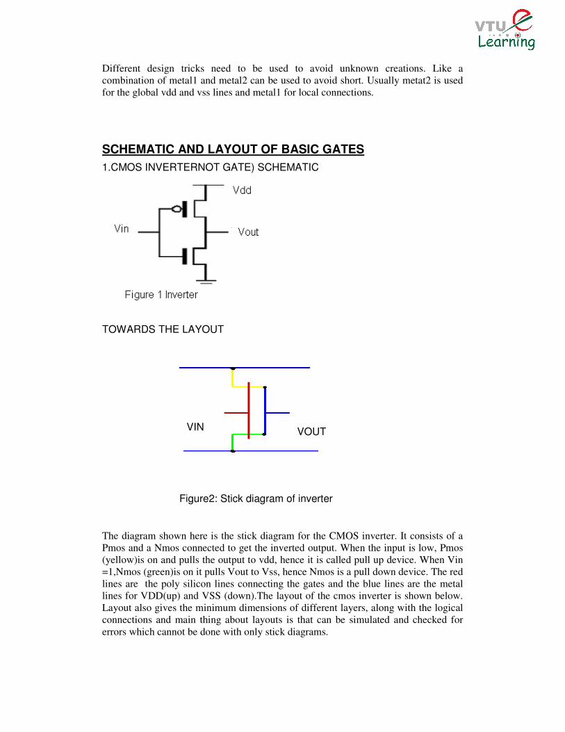
The diagram shown here is the stick diagram for the CMOS inverter. It consists of a
Pmos and a Nmos connected to get the inverted output. When the input is low, Pmos
(yellow)is on and pulls the output to vdd, hence it is called pull up device. When Vin
=1,Nmos (green)is on it pulls Vout to Vss, hence Nmos is a pull down device. The red
lines are the poly silicon lines connecting the gates and the blue lines are the metal
lines for VDD(up) and VSS (down).The layout of the cmos inverter is shown below.
Layout also gives the minimum dimensions of different layers, along with the logical
connections and main thing about layouts is that can be simulated and checked for
errors which cannot be done with only stick diagrams.
VIN VOUT
Figure2: Stick diagram of inverter
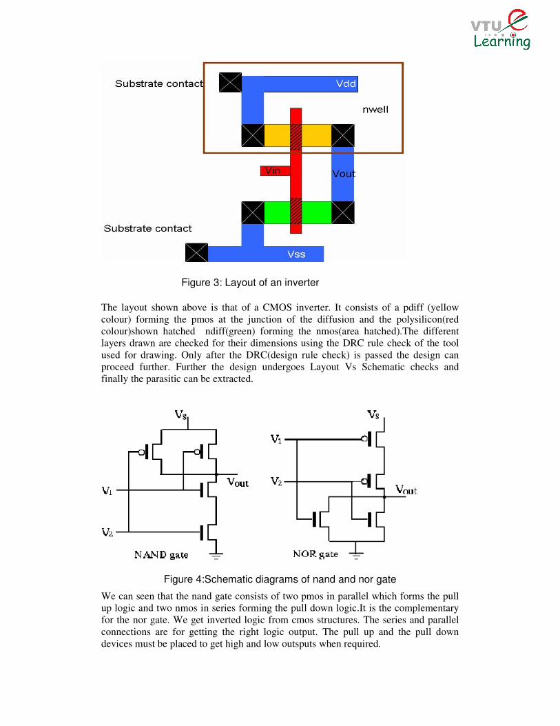
The layout shown above is that of a CMOS inverter. It consists of a pdiff (yellow
colour) forming the pmos at the junction of the diffusion and the polysilicon(red
colour)shown hatched ndiff(green) forming the nmos(area hatched).The different
layers drawn are checked for their dimensions using the DRC rule check of the tool
used for drawing. Only after the DRC(design rule check) is passed the design can
proceed further. Further the design undergoes Layout Vs Schematic checks and
finally the parasitic can be extracted.
Figure 4:Schematic diagrams of nand and nor gate
We can seen that the nand gate consists of two pmos in parallel which forms the pull
up logic and two nmos in series forming the pull down logic.It is the complementary
for the nor gate. We get inverted logic from cmos structures. The series and parallel
connections are for getting the right logic output. The pull up and the pull down
devices must be placed to get high and low outsputs when required.
Figure 3: Layout of an inverter
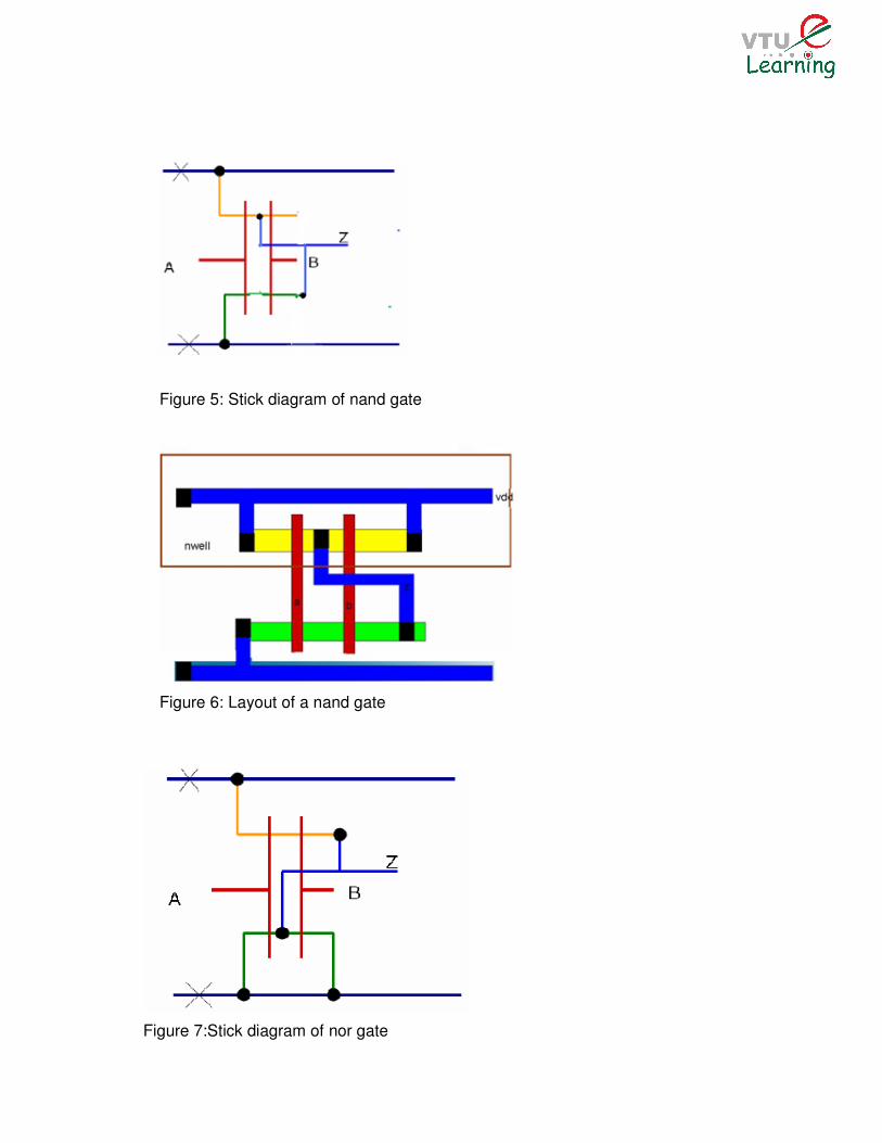
Figure 5: Stick diagram of nand gate
Figure 6: Layout of a nand gate
Figure 7:Stick diagram of nor gate

Figure 8: Layout of nor gate
TRANSMISSION GATE
Figure 9 :Symbol and schematic of transmission gate
Layout considerations of transmission gate. It consist of drains and the sources of the
P&N devices paralleled. Transmission gate can replace the pass transistors and has
the advantage of giving both a good one and a good zero.
Figure 10: Layout of transmissuion gate
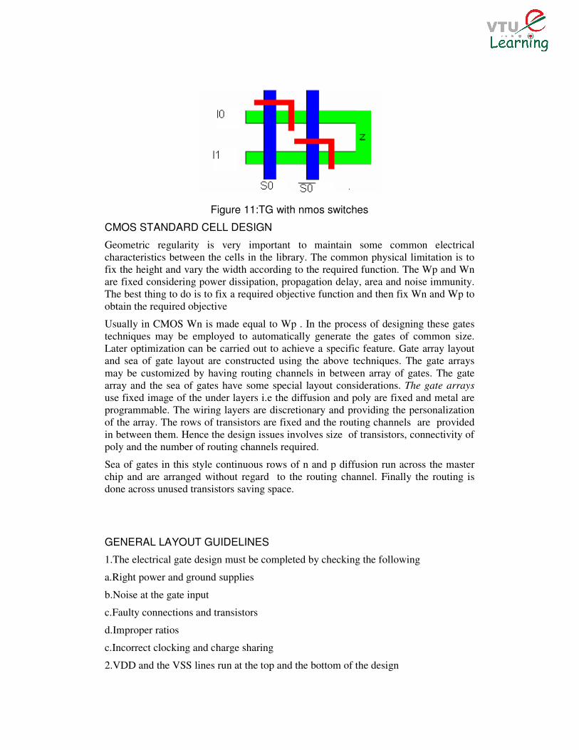
Figure 11:TG with nmos switches
CMOS STANDARD CELL DESIGN
Geometric regularity is very important to maintain some common electrical
characteristics between the cells in the library. The common physical limitation is to
fix the height and vary the width according to the required function. The Wp and Wn
are fixed considering power dissipation, propagation delay, area and noise immunity.
The best thing to do is to fix a required objective function and then fix Wn and Wp to
obtain the required objective
Usually in CMOS Wn is made equal to Wp . In the process of designing these gates
techniques may be employed to automatically generate the gates of common size.
Later optimization can be carried out to achieve a specific feature. Gate array layout
and sea of gate layout are constructed using the above techniques. The gate arrays
may be customized by having routing channels in between array of gates. The gate
array and the sea of gates have some special layout considerations. The gate arrays
use fixed image of the under layers i.e the diffusion and poly are fixed and metal are
programmable. The wiring layers are discretionary and providing the personalization
of the array. The rows of transistors are fixed and the routing channels are provided
in between them. Hence the design issues involves size of transistors, connectivity of
poly and the number of routing channels required.
Sea of gates in this style continuous rows of n and p diffusion run across the master
chip and are arranged without regard to the routing channel. Finally the routing is
done across unused transistors saving space.
GENERAL LAYOUT GUIDELINES
1.The electrical gate design must be completed by checking the following
a.Right power and ground supplies
b.Noise at the gate input
c.Faulty connections and transistors
d.Improper ratios
c.Incorrect clocking and charge sharing
2.VDD and the VSS lines run at the top and the bottom of the design
3.Vertical poysilicon for each gate input
4.Order polysilicon gate signals for maximal connection between transistors
5.The connectivity requires to place nmos close to VSS and pmos close to VDD
6.Connection to complete the logic must be made using poly,metal and even metal2
The design must always proceeds towards optimization. Here optimization is at
transistor level rather then gate level. Since the density of transistors is large ,we
could obtain smaller and faster layout by designing logic blocks of 1000 transistors
instead of considering a single at a time and then putting them together. Density
improvement can also be made by considering optimization of the other factors in the
layout
The factors are
1.Efficient routing space usage. They can be placed over the cells or even in multiple
layers.
2.Source drain connections must be merged better.
3.White (blank) spaces must be minimum
4.The devices must be of optimum sizes.
5.Transperent routing can be provided for cell to cell interconnection, this reduces
global wiring problems
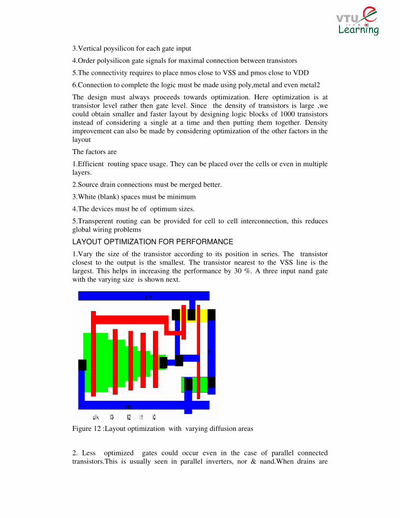
LAYOUT OPTIMIZATION FOR PERFORMANCE
1.Vary the size of the transistor according to its position in series. The transistor
closest to the output is the smallest. The transistor nearest to the VSS line is the
largest. This helps in increasing the performance by 30 %. A three input nand gate
with the varying size is shown next.
Figure 12 :Layout optimization with varying diffusion areas
2. Less optimized gates could occur even in the case of parallel connected
transistors.This is usually seen in parallel inverters, nor & nand.When drains are
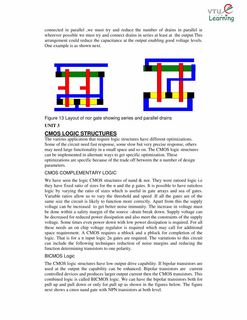
connected in parallel ,we must try and reduce the number of drains in parallel ie
wherever possible we must try and connect drains in series at least at the output.This
arrangement could reduce the capacitance at the output enabling good voltage levels.
One example is as shown next.
Figure 13 Layout of nor gate showing series and parallel drains
UNIT 3
CMOS LOGIC STRUCTURES
The various application that require logic structures have different optimizations.
Some of the circuit need fast response, some slow but very precise response, others
may need large functionality in a small space and so on. The CMOS logic structures
can be implemented in alternate ways to get specific optimization. These
optimizations are specific because of the trade off between the n number of design
parameters.
CMOS COMPLEMENTARY LOGIC
We have seen the logic CMOS structures of nand & nor. They were ratioed logic i.e
they have fixed ratio of sizes for the n and the p gates. It is possible to have ratioless
logic by varying the ratio of sizes which is useful in gate arrays and sea of gates.
Variable ratios allow us to vary the threshold and speed .If all the gates are of the
same size the circuit is likely to function more correctly. Apart from this the supply
voltage can be increased to get better noise immunity. The increase in voltage must
be done within a safety margin of the source –drain break down. Supply voltage can
be decreased for reduced power dissipation and also meet the constraints of the supply
voltage. Some times even power down with low power dissipation is required. For all
these needs an on chip voltage regulator is required which may call for additional
space requirement. A CMOS requires a nblock and a pblock for completion of the
logic. That is for a n input logic 2n gates are required. The variations to this circuit
can include the following techniques reduction of noise margins and reducing the
function determining transistors to one polarity.
BICMOS Logic
The CMOS logic structures have low output drive capability. If bipolar transistors are
used at the output the capability can be enhanced. Bipolar transistors are current
controlled devices and produces larger output current then the CMOS transistors. This
combined logic is called BICMOS logic. We can have the bipolar transistors both for
pull up and pull down or only for pull up as shown in the figures below. The figure
next shows a cmos nand gate with NPN transistors at both level.
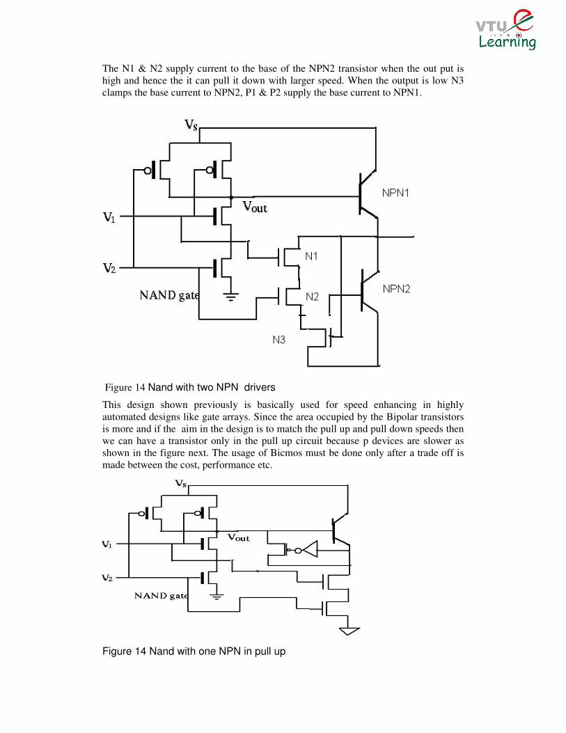
The N1 & N2 supply current to the base of the NPN2 transistor when the out put is
high and hence the it can pull it down with larger speed. When the output is low N3
clamps the base current to NPN2, P1 & P2 supply the base current to NPN1.
Figure 14 Nand with two NPN drivers
This design shown previously is basically used for speed enhancing in highly
automated designs like gate arrays. Since the area occupied by the Bipolar transistors
is more and if the aim in the design is to match the pull up and pull down speeds then
we can have a transistor only in the pull up circuit because p devices are slower as
shown in the figure next. The usage of Bicmos must be done only after a trade off is
made between the cost, performance etc.
Figure 14 Nand with one NPN in pull up
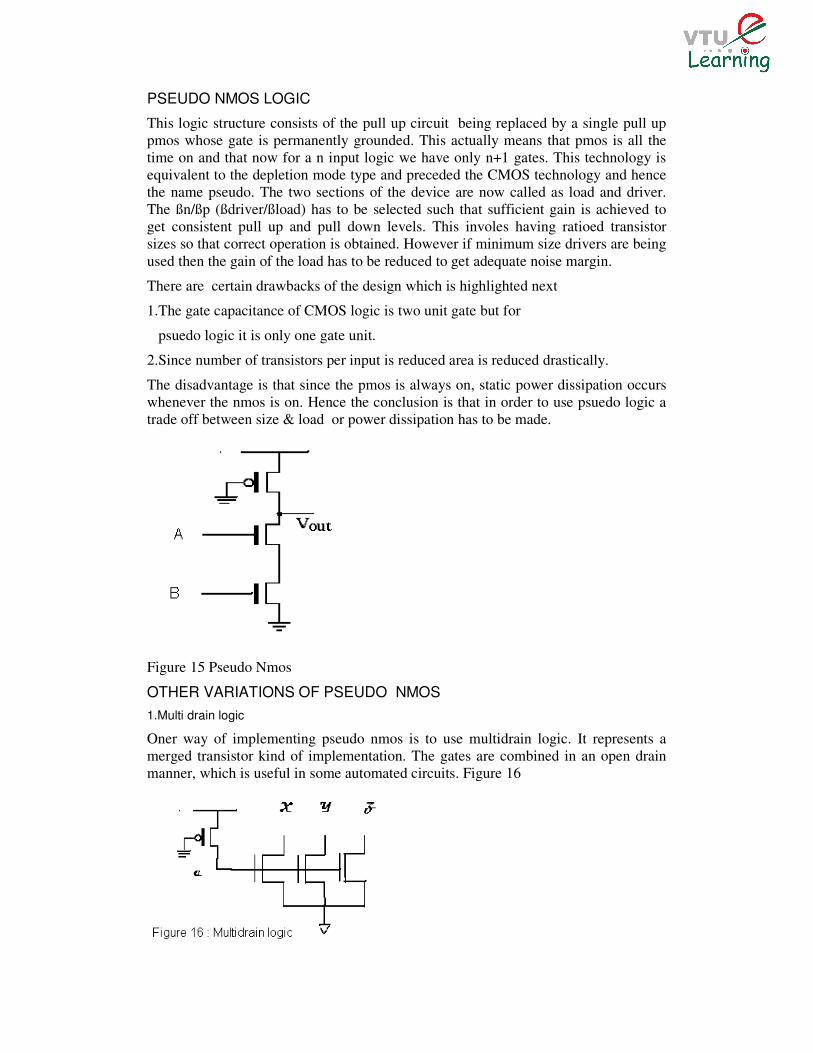
PSEUDO NMOS LOGIC
This logic structure consists of the pull up circuit being replaced by a single pull up
pmos whose gate is permanently grounded. This actually means that pmos is all the
time on and that now for a n input logic we have only n+1 gates. This technology is
equivalent to the depletion mode type and preceded the CMOS technology and hence
the name pseudo. The two sections of the device are now called as load and driver.
The ßn/ßp (ßdriver/ßload) has to be selected such that sufficient gain is achieved to
get consistent pull up and pull down levels. This involes having ratioed transistor
sizes so that correct operation is obtained. However if minimum size drivers are being
used then the gain of the load has to be reduced to get adequate noise margin.
There are certain drawbacks of the design which is highlighted next
1.The gate capacitance of CMOS logic is two unit gate but for
psuedo logic it is only one gate unit.
2.Since number of transistors per input is reduced area is reduced drastically.
The disadvantage is that since the pmos is always on, static power dissipation occurs
whenever the nmos is on. Hence the conclusion is that in order to use psuedo logic a
trade off between size & load or power dissipation has to be made.
Figure 15 Pseudo Nmos
OTHER VARIATIONS OF PSEUDO NMOS
1.Multi drain logic
Oner way of implementing pseudo nmos is to use multidrain logic. It represents a
merged transistor kind of implementation. The gates are combined in an open drain
manner, which is useful in some automated circuits. Figure 16
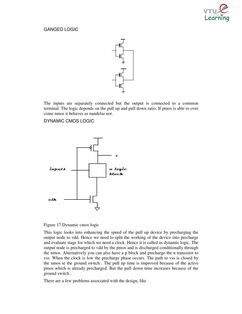
GANGED LOGIC
The inputs are separately connected but the output is connected to a common
terminal. The logic depends on the pull up and pull down ratio. If pmos is able to over
come nmos it behaves as nandelse nor.
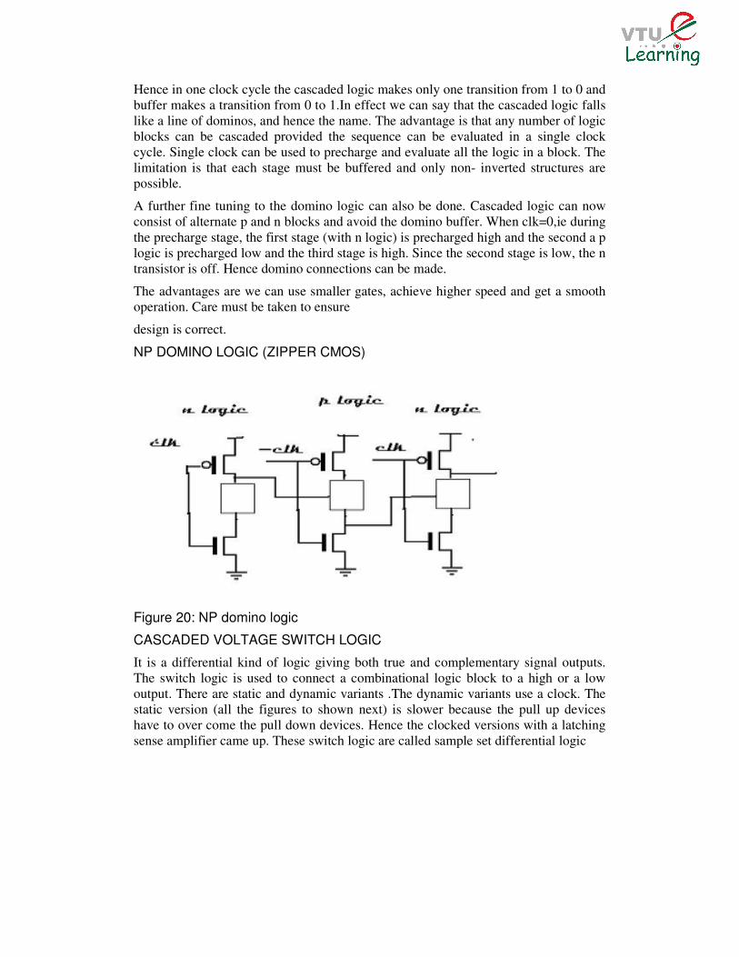
DYNAMIC CMOS LOGIC
Figure 17 Dynamic cmos logic
This logic looks into enhancing the speed of the pull up device by precharging the
output node to vdd. Hence we need to split the working of the device into precharge
and evaluate stage for which we need a clock. Hence it is called as dynamic logic. The
output node is precharged to vdd by the pmos and is discharged conditionally through
the nmos. Alternatively you can also have a p block and precharge the n transistor to
vss. When the clock is low the precharge phase occurs. The path to vss is closed by
the nmos ie the ground switch . The pull up time is improved because of the active
pmos which is already precharged. But the pull down time increases because of the
ground switch .
There are a few problems associated with the design, like

1.Inputs have to change during the precharge stage and must be stable during the
evaluate. If this condition cannot occur then charge redistribution corrupts the output
node.
2.A simple single dynamic logic cannot be cascaded. During the evaluate phase the
first gate will conditionally discharge but by the time the second gate evaluates, there
is going to be a finite delay. By then the first gate may precharge.
CLOCKED CMOS LOGIC (C2MOS)
Figure 18 C2mos logic
CMOS DOMINO LOGIC
The disadvantage associated with the dynamic CMOS is over come in this logic. In
this we are able to cascade logic blocks with the help of a single clock. The precharge
and the evaluate phases retained as they were. The change required is to add a buffer
at the end of each stage.
This logic works in the following manner. When the clk=0,ie during the precharge
stage the output of the dynamic logic is high and the output of the buffer is low. Since
the subsequent stages are fed from the buffer they are all off in the precharge stage.
When the gate is evaluated in the next phase, the output conditionally goes low and
the output of the buffer goes high. The the subsequent gates make a transition from
high to low.
Figure 19:Cmos domino logic
Hence in one clock cycle the cascaded logic makes only one transition from 1 to 0 and
buffer makes a transition from 0 to 1.In effect we can say that the cascaded logic falls
like a line of dominos, and hence the name. The advantage is that any number of logic
blocks can be cascaded provided the sequence can be evaluated in a single clock
cycle. Single clock can be used to precharge and evaluate all the logic in a block. The
limitation is that each stage must be buffered and only non- inverted structures are
possible.
A further fine tuning to the domino logic can also be done. Cascaded logic can now
consist of alternate p and n blocks and avoid the domino buffer. When clk=0,ie during
the precharge stage, the first stage (with n logic) is precharged high and the second a p
logic is precharged low and the third stage is high. Since the second stage is low, the n
transistor is off. Hence domino connections can be made.
The advantages are we can use smaller gates, achieve higher speed and get a smooth
operation. Care must be taken to ensure
design is correct.
NP DOMINO LOGIC (ZIPPER CMOS)
Figure 20: NP domino logic
CASCADED VOLTAGE SWITCH LOGIC
It is a differential kind of logic giving both true and complementary signal outputs.
The switch logic is used to connect a combinational logic block to a high or a low
output. There are static and dynamic variants .The dynamic variants use a clock. The
static version (all the figures to shown next) is slower because the pull up devices
have to over come the pull down devices. Hence the clocked versions with a latching
sense amplifier came up. These switch logic are called sample set differential logic
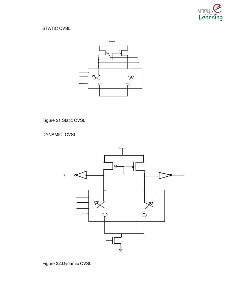
STATIC CVSL
Figure 21 Static CVSL
DYNAMIC CVSL
Figure 22:Dynamic CVSL
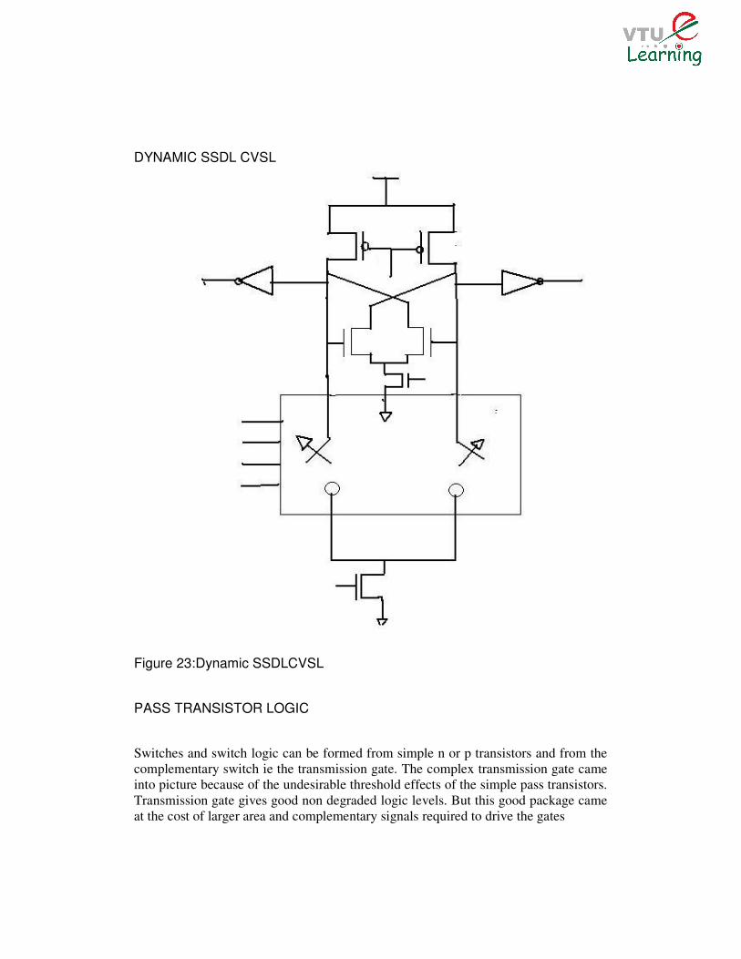
DYNAMIC SSDL CVSL
Figure 23:Dynamic SSDLCVSL
PASS TRANSISTOR LOGIC
Switches and switch logic can be formed from simple n or p transistors and from the
complementary switch ie the transmission gate. The complex transmission gate came
into picture because of the undesirable threshold effects of the simple pass transistors.
Transmission gate gives good non degraded logic levels. But this good package came
at the cost of larger area and complementary signals required to drive the gates
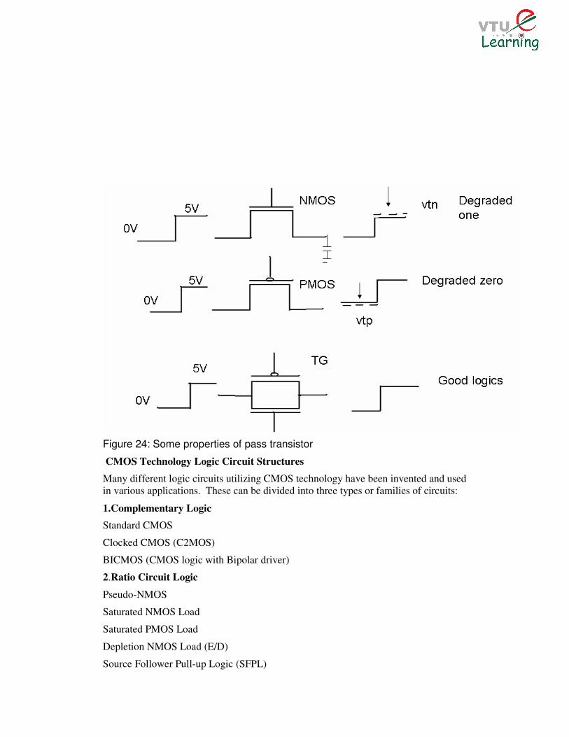
Figure 24: Some properties of pass transistor
CMOS Technology Logic Circuit Structures
Many different logic circuits utilizing CMOS technology have been invented and used
in various applications. These can be divided into three types or families of circuits:
1.Complementary Logic
Standard CMOS
Clocked CMOS (C2MOS)
BICMOS (CMOS logic with Bipolar driver)
2.Ratio Circuit Logic
Pseudo-NMOS
Saturated NMOS Load
Saturated PMOS Load
Depletion NMOS Load (E/D)
Source Follower Pull-up Logic (SFPL)
3.Dynamic Logic:
CMOS Domino Logic
NP Domino Logic (also called Zipper CMOS)
NOR A Logic
Cascade voltage Switch Logic (CVSL)
Sample-Set Differential Logic (SSDL)
Pass-Transistor Logic
The large number of implementations shown so far may lead to a confusion as to what
to use where. Here are some inputs
1.Complementary CMOS
The best option,because of the less dc power dissipation, noise immuned and fast.The
logic is highly automated. Avoid in large fan outs as it leads to excessive levels of
logic.
2.BICMOS
It can be used in high speed applications with large fanout. The economics must be
justified.
PSUEDO –NMOS
Mostly useful in large fan in NOR gates like ROMS,PLA and CLA adders.The DC
power can be reduced to 0 in case of power down situations
Clocked CMOS
Useful in hot electron susceptible processes.
CMOS domino logic
Used mostly in high speed low power application. Care must take of charge
redistribution. Precharge robs the speed advantage.
CVSL
This is basically useful in fast cascaded logic .The size, design complexity and
reduced noise immunity make the design not so popular.
Hybrid designs are also being tried for getting the maximum advantage of each
of them into one.