Optical Retrorefl ective Marker Fabricated on Silicon-On...
11
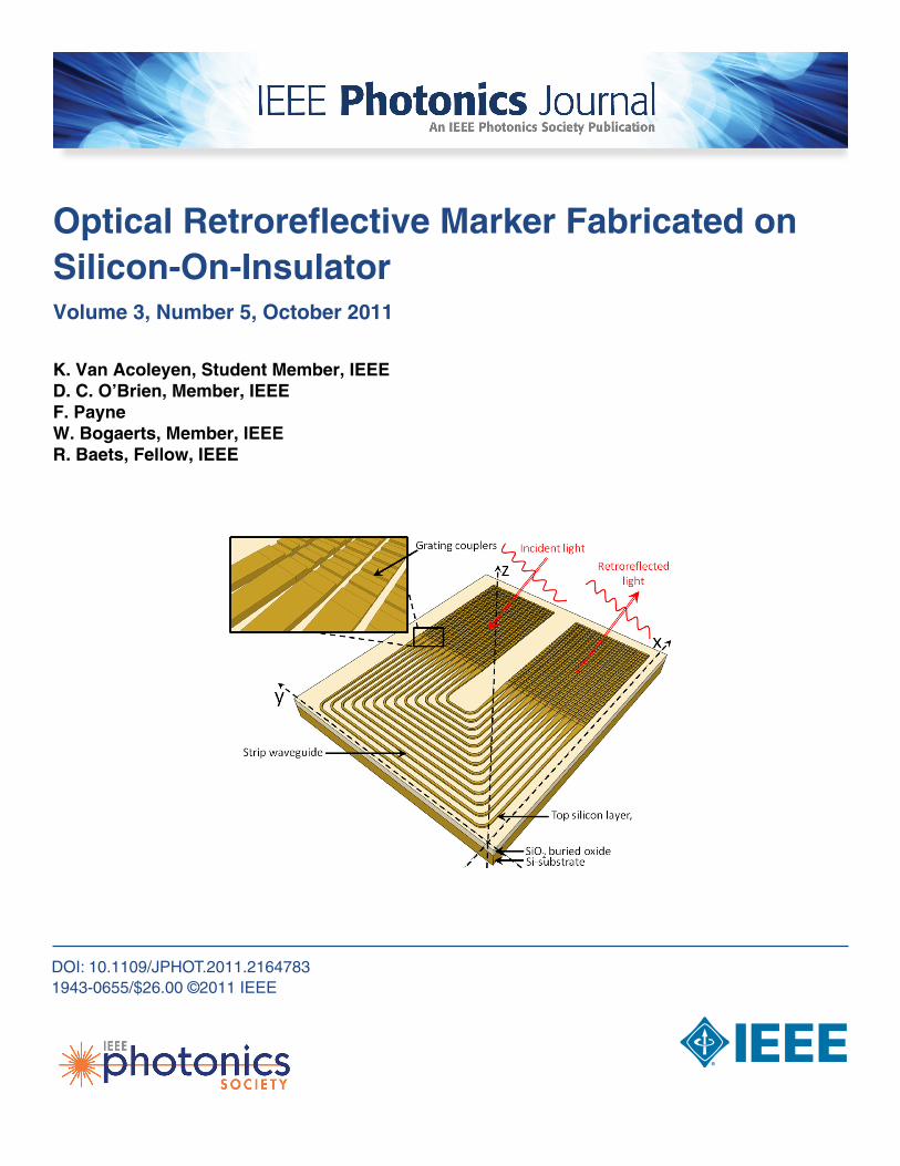
Optical Retroreflective Marker Fabricated on Silicon-On-Insulator Volume 3, Number 5, October 2011 K. Van Acoleyen, Student Member, IEEE D. C. O’Brien, Member, IEEE F. Payne W. Bogaerts, Member, IEEE R. Baets, Fellow, IEEE DOI: 10.1109/JPHOT.2011.2164783 1943-0655/$26.00 ©2011 IEEE
-
Upload
nguyennhan -
Category
Documents
-
view
221 -
download
3
Transcript of Optical Retrorefl ective Marker Fabricated on Silicon-On...
Optical Retrorefl ective Marker Fabricated on Silicon-On-InsulatorVolume 3, Number 5, October 2011
K. Van Acoleyen, Student Member, IEEED. C. O’Brien, Member, IEEEF. PayneW. Bogaerts, Member, IEEER. Baets, Fellow, IEEE
DOI: 10.1109/JPHOT.2011.21647831943-0655/$26.00 ©2011 IEEE

Optical Retroreflective Marker Fabricatedon Silicon-On-Insulator
K. Van Acoleyen,1;2 Student Member, IEEE, D. C. O’Brien,3 Member, IEEE,F. Payne,3 W. Bogaerts,1;2 Member, IEEE, and R. Baets,1;2 Fellow, IEEE
1Photonics Research Group, Department of Information Technology (INTEC),Ghent University-IMEC, 9000 Ghent, Belgium
2Center for Nano- and Biophotonics (NB-Photonics), Ghent University, 9000 Ghent, Belgium3Department of Engineering Science, OX1 3PJ Oxford, U.K.
DOI: 10.1109/JPHOT.2011.21647831943-0655/$26.00 �2011 IEEE
Manuscript received June 30, 2011; revised August 4, 2011; accepted August 5, 2011. Date of publicationAugust 15, 2011; date of current version September 6, 2011. This work was supported by theMethusalemproject BSmart Photonic ICs[ of Ghent University and the Interuniversity Attraction Poles (IAP) projectPhotonics@be. Corresponding author: K. Van Acoleyen (e-mail: [email protected]).
Abstract: Optical retroreflective markers provide a strong return signal when illuminated bya source, resulting in an easy way to localize and identify an object. As current opticalretroreflectors are typically bulky, we have investigated the use of the integrated siliconphotonics platform to fabricate optical retroreflectors. An optical retroreflective marker with atotal field of view (FOV) of about 57� � 4� is shown here. With a limited number of reflectors,a large FOV can then be covered.
Index Terms: Silicon nanophotonics, integrated nanophotonics, free-space communication,waveguide devices.
1. IntroductionOptical retroreflectors provide a versatile way to allow localization and identification of objects or totransmit data using an extra modulating device. Light from a source illuminates the marker, andreturns to it due to the action of the retroreflector. When used as a marker, optics have the inherentadvantage of working at a small wavelength, allowing very precise localization of the markers,compared with radio frequency (RF) approaches. Furthermore, there is no problem of electro-magnetic interference. However, we are limited by the line-of-sight (LOS) constraint and, typically, alimited field of view (FOV). When used as data transmission nodes (e.g., in sensor networks), thenode typically consists of a bulk corner-cube reflector (CCR) or cat’s-eye retroreflector (CERR),together with a transmissive or reflective modulator to impress the data on the retroreflectivesystem. These systems then only require complexity at the base station for tracking the node anddata processing, but the nodes can be kept quite simple, low cost, and lightweight. An example ofsuch a system has been shown in [1], where a corner-cube array is used together with a liquidcrystal modulator to transmit the data of the Bsmart dust motes[ and most of the complexity is in thebase station. An integrated approach to fabricate retroreflectors makes use of microelectromecha-nical systems (MEMS) technology. Such devices are typically useful for short-range applications [2].
In [3], a high contact-angle microdroplet is used to act as a retroreflector with possible applica-tions in optical cross- and interconnects using photonic integration, while in [4], an integrated opticalmarker for simultaneous localization and identification of objects has been demonstrated. The maindrawback in the latter was the limited FOV, which was solved by using a large number of reflectors,each looking in different directions.
Vol. 3, No. 5, October 2011 Page 789
IEEE Photonics Journal Optical Retroreflective Marker

In this paper, we describe the design and fabrication of a fully integrated retroreflector using thesilicon photonics platform. This platform is complementary metal–oxide–semiconductor (CMOS)compatible and attracts a lot of interest for optical interconnects. In [5]–[7], this platform was used tofabricate a chip to free-space interface by using optical phased arrays which allow beam steering[8]. In this paper, a retroreflective structure is proposed as the interface between free-space and thechip. Such an integrated on-chip optical retroreflector has applications in chip-readout schemes,active alignment markers, or free-space cross- and interconnects. It could for example allow datacommunication between different on-chip photonic layers without the need for very sensitivealignment. In the current design, the retroreflector has a large FOV (of about 57�) in one dimension,while the FOV is still limited in the other dimension to about 4�. Only a limited number ofretroreflectors is then needed to cover a large FOV. Achieving omnidirectional retroreflectivity isvery challenging, especially for large angles with respect to the surface normal. By careful design, aFOV of 90� � 90� around the surface normal can be covered with 20–25 retroreflectors. Due to thespecific design, the retroreflectivity is wavelength dependent, which allows identification of theretroreflector. By integrating phase tuners, the reflected light can furthermore be modulated withoutthe need of an external modulator. The proposed design can also act as a free-space opticaldemultiplexer when it is not retroreflecting.
In Section 2, we will discuss the working principle of the retroreflector. In Section 3, the fabricationof the component is described. Section 4 discusses the measurement setup, and in Section 5, themeasurement results are given and discussed. Finally, a conclusion is given in Section 6.
2. Working PrincipleFig. 1 shows a schematic of the retroreflector design. We discuss the working principle of theretroreflector separately in the �x - and �y -direction.
2.1. �x -DirectionLight is coupled on- and off-chip using grating couplers. Grating couplers allow the coupling of
light between an integrated circuit and an optical fiber [9] but act here as an interface between theintegrated retroreflector and free-space. These grating couplers were designed to efficiently couplewith the TE-like mode of the waveguides, and thus, for the remainder of this paper, it is assumed
Fig. 1. Optical retroreflector on silicon-on-insulator.
IEEE Photonics Journal Optical Retroreflective Marker
Vol. 3, No. 5, October 2011 Page 790

that all the light is TE polarized with respect to the retroreflector (main E-field component is Ey ). Alateral cross-sectional view of the grating couplers is shown in Fig. 2. Infrared light coming fromfree-space impinges on the grating couplers and is coupled into the strip waveguide delay linebased on the principle of diffraction. The light is then guided through the delay line and coupled off-chip again using a grating coupler at the other end of the delay line. As both grating couplers ateach end of the delay line are the same, light couples out at the direction of incidence. Using theapproach of [10], a grating can be designed that couples both TE- and TM-light into the negative andpositive x -direction (see Fig. 2), respectively. When strip waveguide delay lines are then added at theother side of the grating, retroreflectivity can be observed for both polarizations.
The grating period determines the retroreflectivity in the �x -direction from the grating equation
sin �x ¼ �gr neff ;gr � �
nct�gr(1)
with �gr the period of the grating, � the free-space wavelength, neff ;gr the effective index of theguided mode in the grating area, and nct the refractive index of the background. By having adifferent grating period, the retroreflector will work at a certain, limited �x -range. Using differentretroreflectors with different grating periods, we can increase the FOV in the �x -direction, as for aspecific wavelength, a different retroreflector will light up depending on the angle of incidence �x .The beam width and FOV of the reflected light in the �x -direction depends on the out-couplingstrength of the grating. As we are working with 70-nm-deep etched gratings, the grating strength ishigh, resulting in a short out-coupling length and, thus, a relatively large full-width at half-maximum(FWHM) beamwidth of about 3�–4�, which is then also the FOVof the retroreflector in the �x -direction.
2.2. �y -DirectionIn Fig. 3, the transversal cross section of the grating coupler arrays is shown. This figure
explains the operation principle of the retroreflector. Light that is coupled in using the gratingcoupler arrays is guided through delay lines and coupled back out through the same grating couplerarrays. Grating couplers 0; 1; . . . ;N� 1 are connected with grating couplers 00;10; . . . ;N� 10,respectively, using strip waveguide delay lines, as can be seen in Fig. 1. Assume a plane waveimpinging on the retroreflector at grating coupler array 1 at an angle �y , as shown on the left side ofFig. 3. There is a phase delay �� between adjacent grating couplers due to the angle of incidence�y . At a wavelength where the delay line difference corresponds to a phase difference of a multipleof 2�, this wavefront, with the corresponding phase delays, is copied to grating coupler array 2, asshown on the right side of Fig. 3. Light will then couple out at the angle of incidence �y , andretroreflectivity will be observed. For this wavelength, a plane wave that is coupled in throughgrating coupler array 1 will thus couple out through grating coupler array 2 at the same angle ofincidence and vice versa.
The retroreflector is the optical analog of a radio-frequency (RF) Van Atta array antenna [11].Such an array consists of equally spaced antennas that are interconnected by feeders of the same
Fig. 2. Lateral cross section of the grating coupler (xz-cut of Fig. 1). Infrared light (red line) coming froma strip waveguide is coupled in/out using a grating coupler.
IEEE Photonics Journal Optical Retroreflective Marker
Vol. 3, No. 5, October 2011 Page 791

length. The received RF signal is then retroreflected at the direction of incidence. For wavelengthindependent operation, the delay lines need to have an equal length. This can be done by usingcrossings as shown in Fig. 4(a) or by using an extra inner loop, as shown in Fig. 4(b). The former willresult in high losses as a lot of crossings are needed, and the latter will make the retroreflector largeas the size of the inner loop scales with the number of grating couplers.
The delay lines between the grating couplers will make the component wavelength dependent.Only when the delay length difference �L corresponds to a multiple of 2� phase difference, willretroreflectivity be observed
2��
neff�L ¼ m2� (2)
with � the free-space wavelength, neff the effective index of the delay lines, and m an integer, whichis also called the order of the Arrayed Waveguide Grating (AWG) that is formed by these delaylines.
The retroreflector behavior in the �y -direction is investigated using a scalar approach. The FOV inthe �y -direction is determined by the FOV of one grating coupler, which is determined by the widthof the grating coupler. The full 1/e mode amplitude width in the y -direction of the fundamental TE-likemode of a 1-�m-wide grating coupler is simulated to be about 0.795 �m at 1550 nm and does notvary much with wavelength. It is this field that is coupled out by the grating coupler in the �y -direction.The FWHM of the far field of one such Gaussian is then 57�, which is the FOV of the retrore-flector shown as the red dashed line in Fig. 5. Using a smaller grating coupler width will result ina larger FOV. The complete retroreflector is then simulated in the �y -direction as two arrays of50 Gaussian with a 1/e width of 0.795 �m, spaced 2 �mandwith an inner spacing of 20 �m, as shownin Figs. 1 and 3.
Fig. 4. Routing of the delay lines when all the delay lines need equal length. (a) Use of crossings. (b) Useof an extra inner loop.
Fig. 3. Working principle of the retroreflector (yz-cut of Fig. 1). Grating couplers 0; 1; . . . ;N� 1 areconnected with grating couplers 00;10; . . . ;N� 10. �� is the phase delay of the impinging plane wavebetween adjacent grating couplers. The incoming wavefront is retroreflected in the same direction.
IEEE Photonics Journal Optical Retroreflective Marker
Vol. 3, No. 5, October 2011 Page 792

A plane wave impinges on the structure and the overlap of the impinging fields with the gratingcoupler mode is calculated. These fields are then guided through the delay lines and couple backoff-chip. The far field of all these (100) Gaussian profiles, taking into account their phase differencecan then be easily calculated and is shown as the full blue line in Fig. 5. In Fig. 5, the structure issimulated for the case that condition (2) is fulfilled. The beam width of the retroreflected field isdetermined by the total size of the grating coupler arrays. The FWHM was simulated to be 0.33�.A second beam can also be seen in Fig. 5(a). This is not a retroreflected beam but is present dueto the sampling of the radiated field. When having an array of radiating apertures, spaced at adistance �, different lobes are emitted at an angle of
arcsin�
�(3)
with � the free-space wavelength. In our case, this results in a lobe spacing of about 50� at� ¼ 1523 nm, which is the spacing visible in Fig. 5(a). This specific wavelength is chosen as it is(one of) the operating wavelengths of our retroreflectors given by (2).
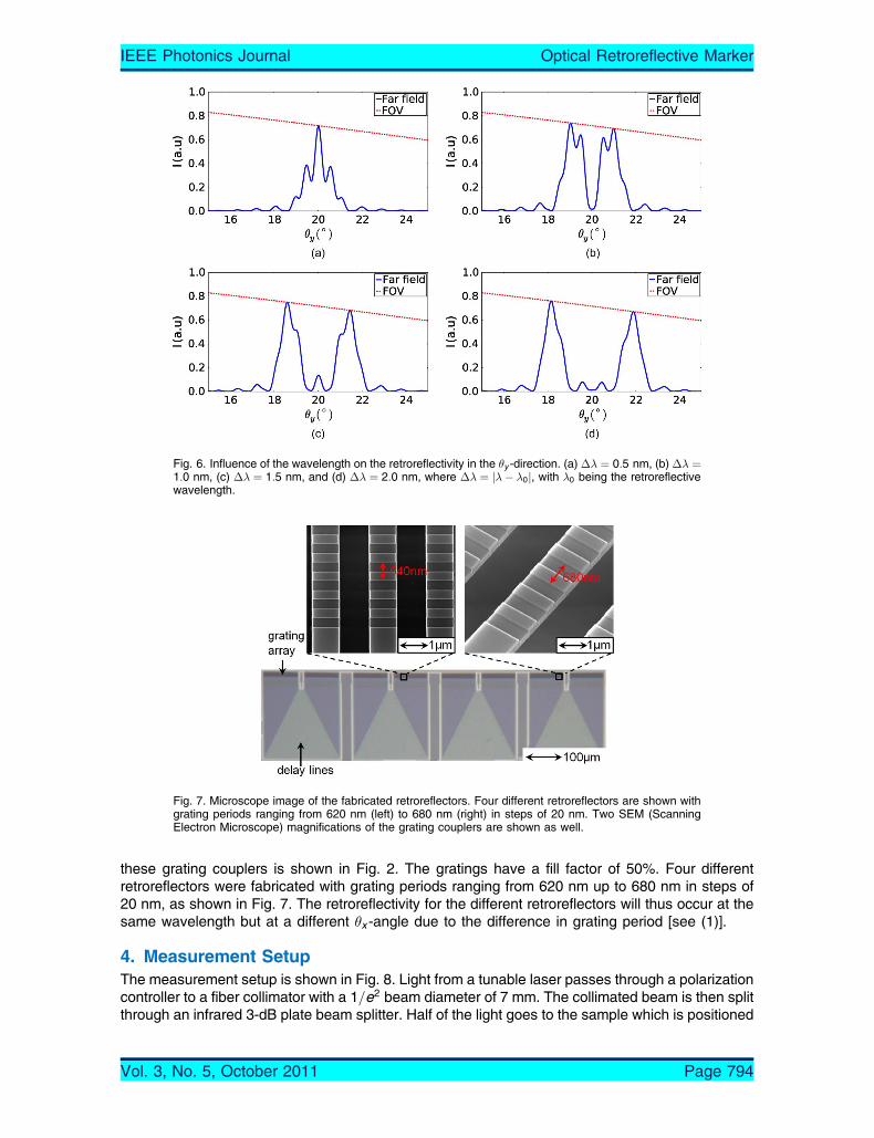
When condition (2) is no longer fulfilled, the demultiplexing effect of the AWG comes into play. InFig. 6, a close up of the far field is shown for different wavelength offsets ��. Two reflected lobesnow arise which move away from the retroreflective direction for increasing wavelength offsets. Ifthe detector only looks at the retroreflective angle, these lobes will quickly move away from thedetector allowing precise localization and identification. The two lobes that are present correspondto the field emitted by grating coupler array 1 and 2 (see Fig. 3). Eventually, they will reach back tothe same retroreflective direction when the condition (2) is again fulfilled, this time for anotherinteger m, which occurs for a wavelength shift of �� ¼ 51 nm.
3. FabricationThe retroreflector shown Fig. 1 was fabricated on silicon-on-insulator (SOI) using standard CMOSprocesses [12], [13]. The buried oxide has a thickness of 2 �m, and the top silicon layer is 220 nmhigh. A deep etch of 220 nm is used to define the waveguides, while a shallow etch of 70 nm is usedto etch the grating couplers. The delay lines have a width of 800 nm, apart from the bends which aretapered to a 450 nm width to allow very sharp bends, with a bend radius down to 3 �m. Awaveguide width of 800 nm is used to reduce phase errors in the delay lines as a wide waveguide ismore tolerant to fabrication errors. The length difference is the same for all retroreflectors and equalto 12 �m. These delay lines form an AWG. Finally, a benzocyclobutene (BCB) layer of about 700 nmis spun on top of the structure, and the structure is covered with a 500-nm gold layer, apart from thegrating coupler areas. This reduces interference arising from diffuse reflected light from other parts ofthe chip.
The grating couplers have a width of 1 �m and are spaced 2 �m apart. The retroreflectors consistof two arrays of 50 grating couplers which are interconnected, as shown in Fig. 1. A cross section of
Fig. 5. (a) Simulated far field of the retroreflector for an impinging wave at �y ¼ 20:0� at � ¼ 1523 nm.The dashed line shows the far field of one grating coupler in the �y -direction being the FOV of theretroreflector in the �y -direction. (b) Magnification of (a) at the retroreflective angle.
IEEE Photonics Journal Optical Retroreflective Marker
Vol. 3, No. 5, October 2011 Page 793
these grating couplers is shown in Fig. 2. The gratings have a fill factor of 50%. Four differentretroreflectors were fabricated with grating periods ranging from 620 nm up to 680 nm in steps of20 nm, as shown in Fig. 7. The retroreflectivity for the different retroreflectors will thus occur at thesame wavelength but at a different �x -angle due to the difference in grating period [see (1)].
4. Measurement SetupThe measurement setup is shown in Fig. 8. Light from a tunable laser passes through a polarizationcontroller to a fiber collimator with a 1=e2 beam diameter of 7 mm. The collimated beam is then splitthrough an infrared 3-dB plate beam splitter. Half of the light goes to the sample which is positioned
Fig. 7. Microscope image of the fabricated retroreflectors. Four different retroreflectors are shown withgrating periods ranging from 620 nm (left) to 680 nm (right) in steps of 20 nm. Two SEM (ScanningElectron Microscope) magnifications of the grating couplers are shown as well.
Fig. 6. Influence of the wavelength on the retroreflectivity in the �y -direction. (a) �� ¼ 0:5 nm, (b) �� ¼1:0 nm, (c) �� ¼ 1:5 nm, and (d) �� ¼ 2:0 nm, where �� ¼ j�� �0j, with �0 being the retroreflectivewavelength.
IEEE Photonics Journal Optical Retroreflective Marker
Vol. 3, No. 5, October 2011 Page 794

in the rotation and tilt center of a motorized rotation and tilt stage. This large beam then illuminatesdifferent retroreflectors. The retroreflected light is then guided back to the 3-dB plate beam splitter,where half of the light will be captured by the microscope and infrared camera. When the lightimpinges perpendicularly on the structure, we get a large reflected beam due to specular reflection.By rotating and tilting the sample, the retroreflected light can be investigated. The numericalaperture (NA) of the microscope is about 0.1, meaning that we will measure the retroreflected lightas long as the reflected light is in a cone with half-angle of 5.7� around the direction of incidence.More light than only the retroreflected light is captured, which is a limitation of our measurementsetup. This can be solved by using a diaphragm to filter out nonretroreflective light.
5. Measurement Results and DiscussionFirst, the retroreflectivity measurements are discussed, then the efficiency with which light iscoupled on/off the chip is investigated, and finally, we touch upon modulation possibilities of thecomponent.
5.1. RetroreflectivityIn Fig. 9, the measured retroreflectivity is shown for different �x -angles. The four different
retroreflectors operate at different �x -angles, while the wavelength is kept constant at 1523 nm. Forthis wavelength, (2) is fulfilled, and retroreflectivity is observed. In these images, the �y -angle is keptconstant at 20�. We can clearly see the two grating coupler arrays of the retroreflectors lighting up atthe same time.
In Fig. 10, the range for which retroreflectivity was measured is given. The chip was rotated todifferent �x - and �y -angles, and the image is then recorded. This image is then integrated and theresult (normalized to 1) is shown as a color plot in Fig. 10. Each retroreflector works for a limited�x -range of about 4�, while the measured �y -range goes from 0� to 25� and, due to symmetryretroreflectivity, will be observed for a span of more than 50�, which compares with the theoreticalFWHM span of 57�. When the �x - and �y -angle reaches 0�, the measurement is saturated by thespecular reflection of the chip; therefore, these small angles are not shown in Fig. 10, but theinfluence of the specular reflection is still visible for small angles.
The retroreflectivity was observed for a wavelength range of about 5 nm around 1523 nm. This isbecause the NA of the microscope captures more light than only the retroreflected light. As thewavelength increases, two lobes arise moving away from the retroreflective direction, as shown inFig. 6, but these two lobes are still captured by the microscope.
5.2. Power EfficiencyWhen used in optical marker applications, one is interested in the power efficiency of these
markers, i.e., the amount of power that is coupled out of the grating couplers off-chip. Therefore,
Fig. 8. Measurement setup to characterize the optical retroreflectors. The infrared light is split through a3-dB splitter illuminating the sample. The sample is positioned in the center of a tilt and rotation stage.The reflected light is captured by a microscope with an infrared camera for different orientations of thesample.
IEEE Photonics Journal Optical Retroreflective Marker
Vol. 3, No. 5, October 2011 Page 795

3-D-Finite Difference Time Domain (FDTD) simulations are performed to investigate the gratingcoupler efficiency as a function of wavelength [14]. The grating is excited with the fundamentalTE-like mode, and the total power flux radiated away from the grating is calculated. The result isshown in Fig. 11. For a grating period of �gr ¼ 620 nm, there is a dip in the efficiency within thecalculated spectral range. This dip is due to Bragg-coupling between the guided mode in the chip
Fig. 10. Measured retroreflectivity range at � ¼ 1523 nm for four different retroreflectors. Eachretroreflector works for a limited �x -range but a large �y -range. (a) �gr ¼ 620 nm, (b) �gr ¼ 640 nm,(c) �gr ¼ 660 nm, and (d) �gr ¼ 680 nm.
Fig. 9. Measured retroreflectivity at different �x -angles at � ¼ 1523 nm. The four different retroreflectorsoperate at the angles (a) �x ¼ 3:0�, (b) �x ¼ 8:8�, (c) �x ¼ 13:0�, and (d) �x ¼ 17:6�. The �y -angle iskept fixed at �y ¼ 20:0�.
IEEE Photonics Journal Optical Retroreflective Marker
Vol. 3, No. 5, October 2011 Page 796

and a surface-normal diffraction order, as well as to the occurrence of second-order couplingbetween the guided mode and its backward mode. For the larger grating periods, this dip shifts tolarger wavelengths and is no longer visible in the graph. The efficiency of the different gratings atthe retroreflective wavelength � ¼ 1523 nm is similar for all retroreflectors and equal to about34%. This efficiency can be increased by using a silicon overlay, which can boost the efficiency tomore than 90% [15].
5.3. ModulationThese retroreflectors can be modulated on-chip to transmit data. The simplest method of modu-
lation is to heat the chip. Silicon has a very high temperature coefficient @n=@T ¼ 1:84 � 10�4 K�1
[16], [17]. By heating up the delay lines, (2) will no longer be fulfilled for the same wavelength, andthe retroreflectivity will disappear, which we have measured experimentally by heating up thecomplete chip. The phase relation could also be destroyed using a liquid crystal [18] or nanoelec-tromechanical systems (NEMS) [19] approach. While these are relatively slow effects, a morepractical approach is to integrate fast carrier-based modulators [20] within the retroreflector todestroy the phase relation between the delay lines and, thus, the retroreflectivity.
6. ConclusionA retroreflector fabricated using the silicon photonics platform has been demonstrated. Eachretroreflector has a FOV of 57� � 4�. A large range can thus be covered with only a limited numberof retroreflectors. The retroreflector is wavelength dependent and acts as a free-space wavelengthdemultiplexer at the nonretroreflective wavelengths. By incorporating phase tuners to destroy thephase relation between the different grating couplers that couple light in and out of the retroreflector,the retroreflective data can be modulated, and data can be transmitted.
AcknowledgmentK. Van Acoleyen acknowledges the Research Foundation–Flanders (FWO) for a research grant.
The authors acknowledge E. Lambert and W. Bogaerts for the LightPy Design Framework. Theauthors would like to thank S. Keyvaninia for the Scanning Electron Microscope (SEM) pictures.
References[1] D. C. O’Brien, J. J. Liu, G. E. Faulkner, S. Sivathasan, W. W. Yuan, S. Collins, and S. J. Elston, BDesign and
implementation of optical wireless communications with optically powered smart dust motes,[ IEEE J. Sel. AreasCommun., vol. 27, no. 9, pp. 1646–1653, Dec. 2009.
[2] P. G. Goetz, W. S. Rabinovich, R. Mahon, L. Swingen, G. C. Gilbreath, J. L. Murphy, H. R. Burris, and M. F. Stell,BPractical considerations of retroreflector choice in modulating retroreflector systems,[ in LEOS Summer TopicalMeeting Dig., New York, 2005, pp. 49–50.
Fig. 11. Three-dimensional-FDTD simulated out-coupling efficiency of one grating coupler for differentgrating periods.
IEEE Photonics Journal Optical Retroreflective Marker
Vol. 3, No. 5, October 2011 Page 797

[3] E. L. Landry, B. Born, G. Ross, and J. F. Holzman, BIntegrated photonic retroreflectors for lateral cross-connects andinterconnects,[ in Proc. 23rd IEEE CCECE, Calgary, AB, Canada, 2010, pp. 1–4.
[4] M. Verbist, W. Bogaerts, J. Schrauwen, and R. Baets, BSilicon-on-insulator-based retroreflective optical marker chipsfor simultaneous identification and localization,[ IEEE J. Sel. Topics Quantum Electron., vol. 15, no. 5, pp. 1427–1431,Sep./Oct. 2009.
[5] K. Van Acoleyen, W. Bogaerts, J. Jagerska, N. Le Thomas, R. Houdre, and R. Baets, BOff-chip beam steering with aone-dimensional optical phased array on silicon-on-insulator,[ Opt. Lett., vol. 34, no. 9, pp. 1477–1479, May 2009.
[6] K. Van Acoleyen, H. Rogier, and R. Baets, BTwo-dimensional optical phased array antenna on silicon-on-insulator,[Opt. Exp., vol. 18, no. 13, pp. 13 655–13 660, Jun. 2010.
[7] K. Van Acoleyen, W. Bogaerts, H. Rogier, and R. Baets, BTwo-dimensional dispersive beam steerer fabricated onsilicon-on-insulator,[ in Proc. 7th Int. Conf. GFP, Beijing, China, 2010, pp. 371–373.
[8] P. F. McManamon, P. J. Bos, M. J. Escuti, J. Heikenfeld, S. Serati, H. K. Xie, and E. A. Watson, BA review of phasedarray steering for narrow-band electrooptical systems,[ Proc. IEEE, vol. 97, no. 6, pp. 1078–1096, Jun. 2009.
[9] G. Roelkens, D. Vermeulen, D. Van Thourhout, R. Baets, S. Brision, P. Lyan, P. Gautier, and J. M. Fedeli, BHighefficiency diffractive grating couplers for interfacing a single mode optical fiber with a nanophotonic silicon-on-insulatorwaveguide circuit,[ Appl. Phys. Lett., vol. 92, no. 13, pp. 131101-1–131101-3, Mar. 2008.
[10] D. Vermeulen, G. Roelkens, and D. Van Thourhout, BGrating structures for simultaneous coupling to TE and TMwaveguide modes,[ U.S. Patent 20 100 322 555, Dec. 12, 2010.
[11] K. Nagai, BVan Atta array antenna device,[ U.S. Patent 3 731 313, May 1, 1973.[12] ePIXfab, The Silicon Photonics Platform, 2011. [Online]. Available: http://www.epixfab.eu/[13] S. K. Selvaraja, P. Jaenen, W. Bogaerts, D. Van Thourhout, P. Dumon, and R. Baets, BFabrication of photonic wire and
crystal circuits in silicon-on-insulator using 193-nm optical lithography,[ J. Lightw. Technol., vol. 27, no. 18, pp. 4076–4083, Sep. 2009.
[14] A. F. Oskooi, D. Roundy, M. Ibanescu, P. Bermel, J. D. Joannopoulos, and S. G. Johnson, BMEEP: A flexible free-software package for electromagnetic simulations by the FDTD method,[ Comput. Phys. Commun., vol. 181, no. 3,pp. 687–702, Mar. 2010.
[15] D. Vermeulen, S. Selvaraja, G. Verheyen, P. Lepage, W. Bogaerts, and G. Roelkens, BHigh-efficiency silicon-on-insulator fiber-to-chip grating couplers using a silicon overlay,[ in Proc. 6th Int. Conf. GFP, San Fransisico, CA, 2009,p. FPd1.
[16] J. Van Campenhout, W. M. J. Green, S. Assefa, and Y. A. Vlasov, BIntegrated NiSi waveguide heaters for CMOS-compatible silicon thermo-optic devices,[ Opt. Lett., vol. 35, no. 7, pp. 1013–1015, Apr. 2010.
[17] R. L. Espinola, M. C. Tsai, J. T. Yardley, and R. M. Osgood, BFast and low-power thermooptic switch on thin silicon-on-insulator,[ IEEE Photon. Technol. Lett., vol. 15, no. 10, pp. 1366–1368, Oct. 2003.
[18] W. De Cort, J. Beeckman, R. James, F. A. Fernandez, R. Baets, and K. Neyts, BTuning silicon-on-insulator ringresonators with in-plane switching liquid crystals,[ J. Opt. Soc. Amer. B, Opt. Phys., vol. 28, no. 1, pp. 79–85, Jan. 2011.
[19] K. Van Acoleyen, J. Roels, T. Claes, D. Van Thourhout, and R. Baets, BNEMS-based optical phase modulatorfabricated on silicon-on-insulator,[ in Proc. 8th Int. Conf. GFP, London, U.K., 2011.
[20] N. N. Feng, S. R. Liao, D. Z. Feng, P. Dong, D. W. Zheng, H. Liang, R. Shafiiha, G. L. Li, J. E. Cunningham,A. V. Krishnamoorthy, and M. Asghari, BHigh speed carrier-depletion modulators with 1.4V-cm V pi L integrated on0.25 mu m silicon-on-insulator waveguides,[ Opt. Exp., vol. 18, no. 8, pp. 7994–7999, Apr. 2010.
IEEE Photonics Journal Optical Retroreflective Marker
Vol. 3, No. 5, October 2011 Page 798