2016.10.24 halvledere - pdf v.01 - DIODE TRANSISTOR SEMICONDUCTOR - Sven Åge Eriksen -...
528
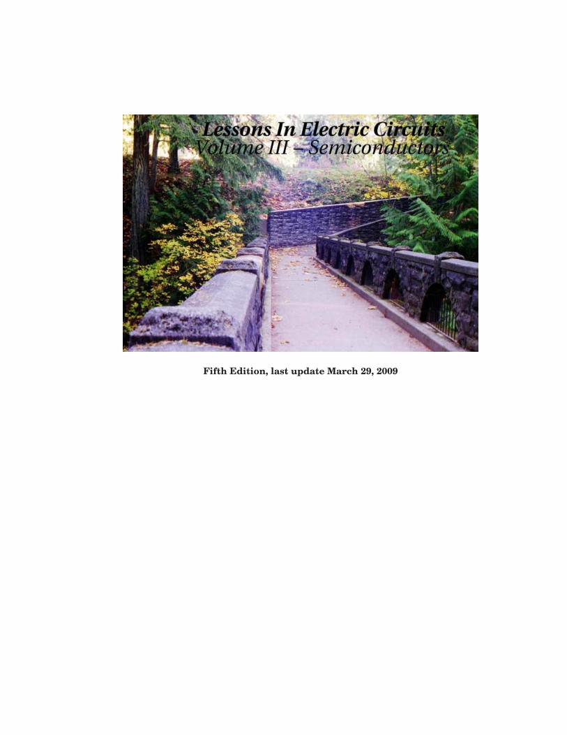
Fifth Edition, last update March 29, 2009
-
Upload
sven-age-eriksen -
Category
Education
-
view
35 -
download
0
Transcript of 2016.10.24 halvledere - pdf v.01 - DIODE TRANSISTOR SEMICONDUCTOR - Sven Åge Eriksen -...
Fifth Edition, last update March 29, 2009

2
Lessons In Electric Circuits, Volume III –
Semiconductors
By Tony R. Kuphaldt
Fifth Edition, last update March 29, 2009

i
c©2000-2015, Tony R. Kuphaldt
This book is published under the terms and conditions of the Design Science License. Theseterms and conditions allow for free copying, distribution, and/or modification of this documentby the general public. The full Design Science License text is included in the last chapter.
As an open and collaboratively developed text, this book is distributed in the hope thatit will be useful, but WITHOUT ANY WARRANTY; without even the implied warranty ofMERCHANTABILITY or FITNESS FOR A PARTICULAR PURPOSE. See the Design ScienceLicense for more details.
Available in its entirety as part of the Open Book Project collection at:
openbookproject.net/electricCircuits
PRINTING HISTORY
• First Edition: Printed in June of 2000. Plain-ASCII illustrations for universal computerreadability.
• Second Edition: Printed in September of 2000. Illustrations reworked in standard graphic(eps and jpeg) format. Source files translated to Texinfo format for easy online and printedpublication.
• Third Edition: Printed in January 2002. Source files translated to SubML format. SubMLis a simple markup language designed to easily convert to other markups like LATEX,HTML, or DocBook using nothing but search-and-replace substitutions.
• Fourth Edition: Printed in December 2002. New sections added, and error correctionsmade, since third edition.
• Fith Edition: Printed in July 2007. New sections added, and error corrections made,format change.

ii
Contents
1 AMPLIFIERS AND ACTIVE DEVICES 1
1.1 From electric to electronic . . . . . . . . . . . . . . . . . . . . . . . . . . . . . . . . 11.2 Active versus passive devices . . . . . . . . . . . . . . . . . . . . . . . . . . . . . . 31.3 Amplifiers . . . . . . . . . . . . . . . . . . . . . . . . . . . . . . . . . . . . . . . . . 31.4 Amplifier gain . . . . . . . . . . . . . . . . . . . . . . . . . . . . . . . . . . . . . . . 61.5 Decibels . . . . . . . . . . . . . . . . . . . . . . . . . . . . . . . . . . . . . . . . . . 81.6 Absolute dB scales . . . . . . . . . . . . . . . . . . . . . . . . . . . . . . . . . . . . 141.7 Attenuators . . . . . . . . . . . . . . . . . . . . . . . . . . . . . . . . . . . . . . . . 16
2 SOLID-STATE DEVICE THEORY 27
2.1 Introduction . . . . . . . . . . . . . . . . . . . . . . . . . . . . . . . . . . . . . . . . 272.2 Quantum physics . . . . . . . . . . . . . . . . . . . . . . . . . . . . . . . . . . . . . 282.3 Valence and Crystal structure . . . . . . . . . . . . . . . . . . . . . . . . . . . . . 412.4 Band theory of solids . . . . . . . . . . . . . . . . . . . . . . . . . . . . . . . . . . . 472.5 Electrons and “holes” . . . . . . . . . . . . . . . . . . . . . . . . . . . . . . . . . . . 502.6 The P-N junction . . . . . . . . . . . . . . . . . . . . . . . . . . . . . . . . . . . . . 552.7 Junction diodes . . . . . . . . . . . . . . . . . . . . . . . . . . . . . . . . . . . . . . 582.8 Bipolar junction transistors . . . . . . . . . . . . . . . . . . . . . . . . . . . . . . . 602.9 Junction field-effect transistors . . . . . . . . . . . . . . . . . . . . . . . . . . . . . 652.10 Insulated-gate field-effect transistors (MOSFET) . . . . . . . . . . . . . . . . . . 702.11 Thyristors . . . . . . . . . . . . . . . . . . . . . . . . . . . . . . . . . . . . . . . . . 732.12 Semiconductor manufacturing techniques . . . . . . . . . . . . . . . . . . . . . . 752.13 Superconducting devices . . . . . . . . . . . . . . . . . . . . . . . . . . . . . . . . . 802.14 Quantum devices . . . . . . . . . . . . . . . . . . . . . . . . . . . . . . . . . . . . . 832.15 Semiconductor devices in SPICE . . . . . . . . . . . . . . . . . . . . . . . . . . . . 91Bibliography . . . . . . . . . . . . . . . . . . . . . . . . . . . . . . . . . . . . . . . . . . . 93
3 DIODES AND RECTIFIERS 97
3.1 Introduction . . . . . . . . . . . . . . . . . . . . . . . . . . . . . . . . . . . . . . . . 983.2 Meter check of a diode . . . . . . . . . . . . . . . . . . . . . . . . . . . . . . . . . . 1033.3 Diode ratings . . . . . . . . . . . . . . . . . . . . . . . . . . . . . . . . . . . . . . . 1073.4 Rectifier circuits . . . . . . . . . . . . . . . . . . . . . . . . . . . . . . . . . . . . . 1083.5 Peak detector . . . . . . . . . . . . . . . . . . . . . . . . . . . . . . . . . . . . . . . 1153.6 Clipper circuits . . . . . . . . . . . . . . . . . . . . . . . . . . . . . . . . . . . . . . 117
iii
iv CONTENTS
3.7 Clamper circuits . . . . . . . . . . . . . . . . . . . . . . . . . . . . . . . . . . . . . 1213.8 Voltage multipliers . . . . . . . . . . . . . . . . . . . . . . . . . . . . . . . . . . . . 1233.9 Inductor commutating circuits . . . . . . . . . . . . . . . . . . . . . . . . . . . . . 1303.10 Diode switching circuits . . . . . . . . . . . . . . . . . . . . . . . . . . . . . . . . . 1323.11 Zener diodes . . . . . . . . . . . . . . . . . . . . . . . . . . . . . . . . . . . . . . . . 1353.12 Special-purpose diodes . . . . . . . . . . . . . . . . . . . . . . . . . . . . . . . . . . 1433.13 Other diode technologies . . . . . . . . . . . . . . . . . . . . . . . . . . . . . . . . . 1633.14 SPICE models . . . . . . . . . . . . . . . . . . . . . . . . . . . . . . . . . . . . . . . 163Bibliography . . . . . . . . . . . . . . . . . . . . . . . . . . . . . . . . . . . . . . . . . . . 172
4 BIPOLAR JUNCTION TRANSISTORS 175
4.1 Introduction . . . . . . . . . . . . . . . . . . . . . . . . . . . . . . . . . . . . . . . . 1764.2 The transistor as a switch . . . . . . . . . . . . . . . . . . . . . . . . . . . . . . . . 1784.3 Meter check of a transistor . . . . . . . . . . . . . . . . . . . . . . . . . . . . . . . 1814.4 Active mode operation . . . . . . . . . . . . . . . . . . . . . . . . . . . . . . . . . . 1854.5 The common-emitter amplifier . . . . . . . . . . . . . . . . . . . . . . . . . . . . . 1914.6 The common-collector amplifier . . . . . . . . . . . . . . . . . . . . . . . . . . . . . 2044.7 The common-base amplifier . . . . . . . . . . . . . . . . . . . . . . . . . . . . . . . 2124.8 The cascode amplifier . . . . . . . . . . . . . . . . . . . . . . . . . . . . . . . . . . 2204.9 Biasing techniques . . . . . . . . . . . . . . . . . . . . . . . . . . . . . . . . . . . . 2244.10 Biasing calculations . . . . . . . . . . . . . . . . . . . . . . . . . . . . . . . . . . . 2374.11 Input and output coupling . . . . . . . . . . . . . . . . . . . . . . . . . . . . . . . . 2494.12 Feedback . . . . . . . . . . . . . . . . . . . . . . . . . . . . . . . . . . . . . . . . . . 2584.13 Amplifier impedances . . . . . . . . . . . . . . . . . . . . . . . . . . . . . . . . . . 2654.14 Current mirrors . . . . . . . . . . . . . . . . . . . . . . . . . . . . . . . . . . . . . . 2664.15 Transistor ratings and packages . . . . . . . . . . . . . . . . . . . . . . . . . . . . 2714.16 BJT quirks . . . . . . . . . . . . . . . . . . . . . . . . . . . . . . . . . . . . . . . . . 273Bibliography . . . . . . . . . . . . . . . . . . . . . . . . . . . . . . . . . . . . . . . . . . . 280
5 JUNCTION FIELD-EFFECT TRANSISTORS 283
5.1 Introduction . . . . . . . . . . . . . . . . . . . . . . . . . . . . . . . . . . . . . . . . 2835.2 The transistor as a switch . . . . . . . . . . . . . . . . . . . . . . . . . . . . . . . . 2855.3 Meter check of a transistor . . . . . . . . . . . . . . . . . . . . . . . . . . . . . . . 2885.4 Active-mode operation . . . . . . . . . . . . . . . . . . . . . . . . . . . . . . . . . . 2905.5 The common-source amplifier – PENDING . . . . . . . . . . . . . . . . . . . . . . 2995.6 The common-drain amplifier – PENDING . . . . . . . . . . . . . . . . . . . . . . 3005.7 The common-gate amplifier – PENDING . . . . . . . . . . . . . . . . . . . . . . . 3005.8 Biasing techniques – PENDING . . . . . . . . . . . . . . . . . . . . . . . . . . . . 3005.9 Transistor ratings and packages – PENDING . . . . . . . . . . . . . . . . . . . . 3015.10 JFET quirks – PENDING . . . . . . . . . . . . . . . . . . . . . . . . . . . . . . . . 301
6 INSULATED-GATE FIELD-EFFECT TRANSISTORS 303
6.1 Introduction . . . . . . . . . . . . . . . . . . . . . . . . . . . . . . . . . . . . . . . . 3036.2 Depletion-type IGFETs . . . . . . . . . . . . . . . . . . . . . . . . . . . . . . . . . 3046.3 Enhancement-type IGFETs – PENDING . . . . . . . . . . . . . . . . . . . . . . . 3136.4 Active-mode operation – PENDING . . . . . . . . . . . . . . . . . . . . . . . . . . 313
CONTENTS v
6.5 The common-source amplifier – PENDING . . . . . . . . . . . . . . . . . . . . . . 3146.6 The common-drain amplifier – PENDING . . . . . . . . . . . . . . . . . . . . . . 3146.7 The common-gate amplifier – PENDING . . . . . . . . . . . . . . . . . . . . . . . 3146.8 Biasing techniques – PENDING . . . . . . . . . . . . . . . . . . . . . . . . . . . . 3146.9 Transistor ratings and packages – PENDING . . . . . . . . . . . . . . . . . . . . 3146.10 IGFET quirks – PENDING . . . . . . . . . . . . . . . . . . . . . . . . . . . . . . . 3156.11 MESFETs – PENDING . . . . . . . . . . . . . . . . . . . . . . . . . . . . . . . . . 3156.12 IGBTs . . . . . . . . . . . . . . . . . . . . . . . . . . . . . . . . . . . . . . . . . . . 315
7 THYRISTORS 319
7.1 Hysteresis . . . . . . . . . . . . . . . . . . . . . . . . . . . . . . . . . . . . . . . . . 3197.2 Gas discharge tubes . . . . . . . . . . . . . . . . . . . . . . . . . . . . . . . . . . . 3207.3 The Shockley Diode . . . . . . . . . . . . . . . . . . . . . . . . . . . . . . . . . . . . 3247.4 The DIAC . . . . . . . . . . . . . . . . . . . . . . . . . . . . . . . . . . . . . . . . . 3317.5 The Silicon-Controlled Rectifier (SCR) . . . . . . . . . . . . . . . . . . . . . . . . . 3317.6 The TRIAC . . . . . . . . . . . . . . . . . . . . . . . . . . . . . . . . . . . . . . . . 3437.7 Optothyristors . . . . . . . . . . . . . . . . . . . . . . . . . . . . . . . . . . . . . . . 3467.8 The Unijunction Transistor (UJT) . . . . . . . . . . . . . . . . . . . . . . . . . . . 3467.9 The Silicon-Controlled Switch (SCS) . . . . . . . . . . . . . . . . . . . . . . . . . . 3527.10 Field-effect-controlled thyristors . . . . . . . . . . . . . . . . . . . . . . . . . . . . 354Bibliography . . . . . . . . . . . . . . . . . . . . . . . . . . . . . . . . . . . . . . . . . . . 356
8 OPERATIONAL AMPLIFIERS 357
8.1 Introduction . . . . . . . . . . . . . . . . . . . . . . . . . . . . . . . . . . . . . . . . 3578.2 Single-ended and differential amplifiers . . . . . . . . . . . . . . . . . . . . . . . . 3588.3 The ”operational” amplifier . . . . . . . . . . . . . . . . . . . . . . . . . . . . . . . 3628.4 Negative feedback . . . . . . . . . . . . . . . . . . . . . . . . . . . . . . . . . . . . 3688.5 Divided feedback . . . . . . . . . . . . . . . . . . . . . . . . . . . . . . . . . . . . . 3718.6 An analogy for divided feedback . . . . . . . . . . . . . . . . . . . . . . . . . . . . 3748.7 Voltage-to-current signal conversion . . . . . . . . . . . . . . . . . . . . . . . . . . 3808.8 Averager and summer circuits . . . . . . . . . . . . . . . . . . . . . . . . . . . . . 3828.9 Building a differential amplifier . . . . . . . . . . . . . . . . . . . . . . . . . . . . 3848.10 The instrumentation amplifier . . . . . . . . . . . . . . . . . . . . . . . . . . . . . 3868.11 Differentiator and integrator circuits . . . . . . . . . . . . . . . . . . . . . . . . . 3878.12 Positive feedback . . . . . . . . . . . . . . . . . . . . . . . . . . . . . . . . . . . . . 3908.13 Practical considerations . . . . . . . . . . . . . . . . . . . . . . . . . . . . . . . . . 3948.14 Operational amplifier models . . . . . . . . . . . . . . . . . . . . . . . . . . . . . . 4108.15 Data . . . . . . . . . . . . . . . . . . . . . . . . . . . . . . . . . . . . . . . . . . . . 415
9 PRACTICAL ANALOG SEMICONDUCTOR CIRCUITS 417
9.1 ElectroStatic Discharge . . . . . . . . . . . . . . . . . . . . . . . . . . . . . . . . . 4179.2 Power supply circuits – INCOMPLETE . . . . . . . . . . . . . . . . . . . . . . . . 4229.3 Amplifier circuits – PENDING . . . . . . . . . . . . . . . . . . . . . . . . . . . . . 4249.4 Oscillator circuits – INCOMPLETE . . . . . . . . . . . . . . . . . . . . . . . . . . 4249.5 Phase-locked loops – PENDING . . . . . . . . . . . . . . . . . . . . . . . . . . . . 4269.6 Radio circuits – INCOMPLETE . . . . . . . . . . . . . . . . . . . . . . . . . . . . . 426

vi CONTENTS
9.7 Computational circuits . . . . . . . . . . . . . . . . . . . . . . . . . . . . . . . . . . 4359.8 Measurement circuits – INCOMPLETE . . . . . . . . . . . . . . . . . . . . . . . . 4579.9 Control circuits – PENDING . . . . . . . . . . . . . . . . . . . . . . . . . . . . . . 458Bibliography . . . . . . . . . . . . . . . . . . . . . . . . . . . . . . . . . . . . . . . . . . . 458
10 ACTIVE FILTERS 461
11 DC MOTOR DRIVES 463
11.1 Pulse Width Modulation . . . . . . . . . . . . . . . . . . . . . . . . . . . . . . . . . 463
12 INVERTERS AND AC MOTOR DRIVES 467
13 ELECTRON TUBES 469
13.1 Introduction . . . . . . . . . . . . . . . . . . . . . . . . . . . . . . . . . . . . . . . . 46913.2 Early tube history . . . . . . . . . . . . . . . . . . . . . . . . . . . . . . . . . . . . 47013.3 The triode . . . . . . . . . . . . . . . . . . . . . . . . . . . . . . . . . . . . . . . . . 47313.4 The tetrode . . . . . . . . . . . . . . . . . . . . . . . . . . . . . . . . . . . . . . . . 47513.5 Beam power tubes . . . . . . . . . . . . . . . . . . . . . . . . . . . . . . . . . . . . 47613.6 The pentode . . . . . . . . . . . . . . . . . . . . . . . . . . . . . . . . . . . . . . . . 47813.7 Combination tubes . . . . . . . . . . . . . . . . . . . . . . . . . . . . . . . . . . . . 47813.8 Tube parameters . . . . . . . . . . . . . . . . . . . . . . . . . . . . . . . . . . . . . 48113.9 Ionization (gas-filled) tubes . . . . . . . . . . . . . . . . . . . . . . . . . . . . . . . 48313.10Display tubes . . . . . . . . . . . . . . . . . . . . . . . . . . . . . . . . . . . . . . . 48713.11Microwave tubes . . . . . . . . . . . . . . . . . . . . . . . . . . . . . . . . . . . . . 49013.12Tubes versus Semiconductors . . . . . . . . . . . . . . . . . . . . . . . . . . . . . . 493
A-1 ABOUT THIS BOOK 497
A-2 CONTRIBUTOR LIST 501
A-3 DESIGN SCIENCE LICENSE 509
INDEX 513
Chapter 1
AMPLIFIERS AND ACTIVE
DEVICES
Contents
1.1 From electric to electronic . . . . . . . . . . . . . . . . . . . . . . . . . . . . . 1
1.2 Active versus passive devices . . . . . . . . . . . . . . . . . . . . . . . . . . . 3
1.3 Amplifiers . . . . . . . . . . . . . . . . . . . . . . . . . . . . . . . . . . . . . . . . 3
1.4 Amplifier gain . . . . . . . . . . . . . . . . . . . . . . . . . . . . . . . . . . . . . 6
1.5 Decibels . . . . . . . . . . . . . . . . . . . . . . . . . . . . . . . . . . . . . . . . . 8
1.6 Absolute dB scales . . . . . . . . . . . . . . . . . . . . . . . . . . . . . . . . . . 14
1.7 Attenuators . . . . . . . . . . . . . . . . . . . . . . . . . . . . . . . . . . . . . . 16
1.7.1 Decibels . . . . . . . . . . . . . . . . . . . . . . . . . . . . . . . . . . . . . 17
1.7.2 T-section attenuator . . . . . . . . . . . . . . . . . . . . . . . . . . . . . . . 19
1.7.3 PI-section attenuator . . . . . . . . . . . . . . . . . . . . . . . . . . . . . . 20
1.7.4 L-section attenuator . . . . . . . . . . . . . . . . . . . . . . . . . . . . . . 21
1.7.5 Bridged T attenuator . . . . . . . . . . . . . . . . . . . . . . . . . . . . . . 21
1.7.6 Cascaded sections . . . . . . . . . . . . . . . . . . . . . . . . . . . . . . . 23
1.7.7 RF attenuators . . . . . . . . . . . . . . . . . . . . . . . . . . . . . . . . . 23
1.1 From electric to electronic
This third volume of the book series Lessons In Electric Circuits makes a departure from theformer two in that the transition between electric circuits and electronic circuits is formallycrossed. Electric circuits are connections of conductive wires and other devices whereby theuniform flow of electrons occurs. Electronic circuits add a new dimension to electric circuitsin that some means of control is exerted over the flow of electrons by another electrical signal,either a voltage or a current.
1
2 CHAPTER 1. AMPLIFIERS AND ACTIVE DEVICES
In and of itself, the control of electron flow is nothing new to the student of electric cir-cuits. Switches control the flow of electrons, as do potentiometers, especially when connectedas variable resistors (rheostats). Neither the switch nor the potentiometer should be new toyour experience by this point in your study. The threshold marking the transition from electricto electronic, then, is defined by how the flow of electrons is controlled rather than whether ornot any form of control exists in a circuit. Switches and rheostats control the flow of electronsaccording to the positioning of a mechanical device, which is actuated by some physical forceexternal to the circuit. In electronics, however, we are dealing with special devices able to con-trol the flow of electrons according to another flow of electrons, or by the application of a staticvoltage. In other words, in an electronic circuit, electricity is able to control electricity.
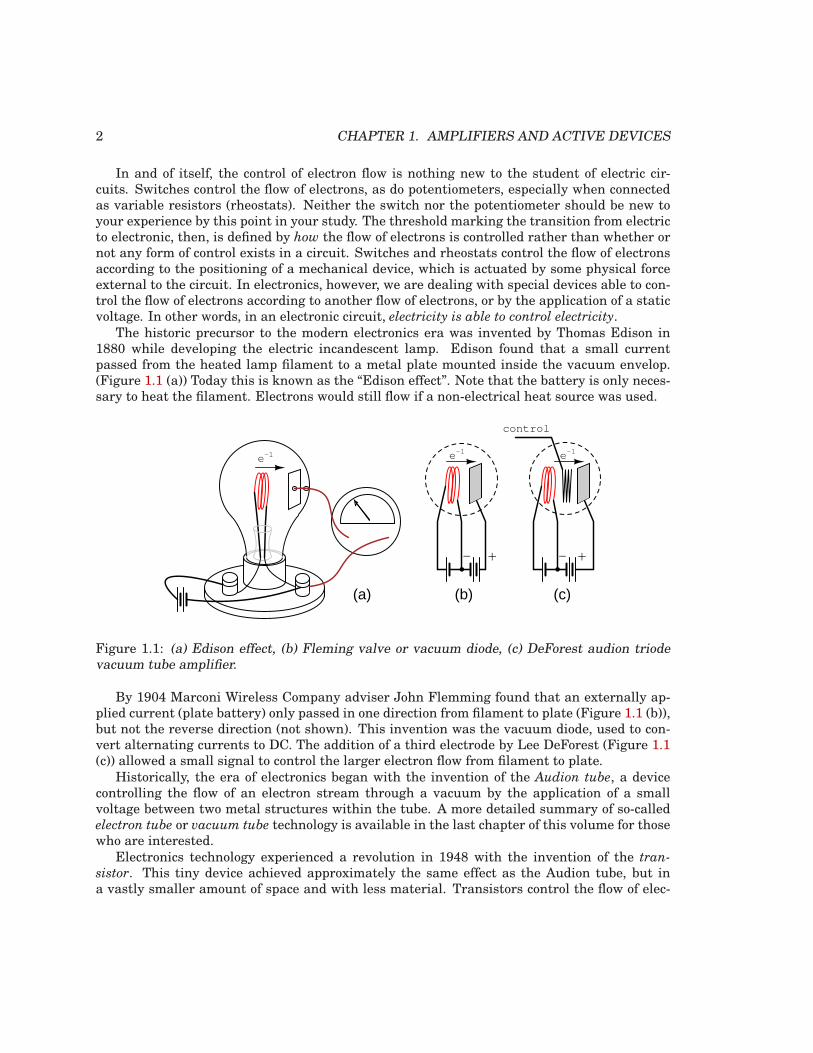
The historic precursor to the modern electronics era was invented by Thomas Edison in1880 while developing the electric incandescent lamp. Edison found that a small currentpassed from the heated lamp filament to a metal plate mounted inside the vacuum envelop.(Figure 1.1 (a)) Today this is known as the “Edison effect”. Note that the battery is only neces-sary to heat the filament. Electrons would still flow if a non-electrical heat source was used.
(a) (b)
+-
(c)
+-
e-1 e-1 e-1
control
Figure 1.1: (a) Edison effect, (b) Fleming valve or vacuum diode, (c) DeForest audion triodevacuum tube amplifier.
By 1904 Marconi Wireless Company adviser John Flemming found that an externally ap-plied current (plate battery) only passed in one direction from filament to plate (Figure 1.1 (b)),but not the reverse direction (not shown). This invention was the vacuum diode, used to con-vert alternating currents to DC. The addition of a third electrode by Lee DeForest (Figure 1.1(c)) allowed a small signal to control the larger electron flow from filament to plate.
Historically, the era of electronics began with the invention of the Audion tube, a devicecontrolling the flow of an electron stream through a vacuum by the application of a smallvoltage between two metal structures within the tube. A more detailed summary of so-calledelectron tube or vacuum tube technology is available in the last chapter of this volume for thosewho are interested.
Electronics technology experienced a revolution in 1948 with the invention of the tran-
sistor. This tiny device achieved approximately the same effect as the Audion tube, but ina vastly smaller amount of space and with less material. Transistors control the flow of elec-
1.2. ACTIVE VERSUS PASSIVE DEVICES 3
trons through solid semiconductor substances rather than through a vacuum, and so transistortechnology is often referred to as solid-state electronics.
1.2 Active versus passive devices
An active device is any type of circuit component with the ability to electrically control electronflow (electricity controlling electricity). In order for a circuit to be properly called electronic,it must contain at least one active device. Components incapable of controlling current bymeans of another electrical signal are called passive devices. Resistors, capacitors, inductors,transformers, and even diodes are all considered passive devices. Active devices include, butare not limited to, vacuum tubes, transistors, silicon-controlled rectifiers (SCRs), and TRIACs.A case might be made for the saturable reactor to be defined as an active device, since it is ableto control an AC current with a DC current, but I’ve never heard it referred to as such. Theoperation of each of these active devices will be explored in later chapters of this volume.
All active devices control the flow of electrons through them. Some active devices allow avoltage to control this current while other active devices allow another current to do the job.Devices utilizing a static voltage as the controlling signal are, not surprisingly, called voltage-
controlled devices. Devices working on the principle of one current controlling another currentare known as current-controlled devices. For the record, vacuum tubes are voltage-controlleddevices while transistors are made as either voltage-controlled or current controlled types. Thefirst type of transistor successfully demonstrated was a current-controlled device.
1.3 Amplifiers
The practical benefit of active devices is their amplifying ability. Whether the device in ques-tion be voltage-controlled or current-controlled, the amount of power required of the control-ling signal is typically far less than the amount of power available in the controlled current.In other words, an active device doesn’t just allow electricity to control electricity; it allows asmall amount of electricity to control a large amount of electricity.
Because of this disparity between controlling and controlled powers, active devices may beemployed to govern a large amount of power (controlled) by the application of a small amountof power (controlling). This behavior is known as amplification.
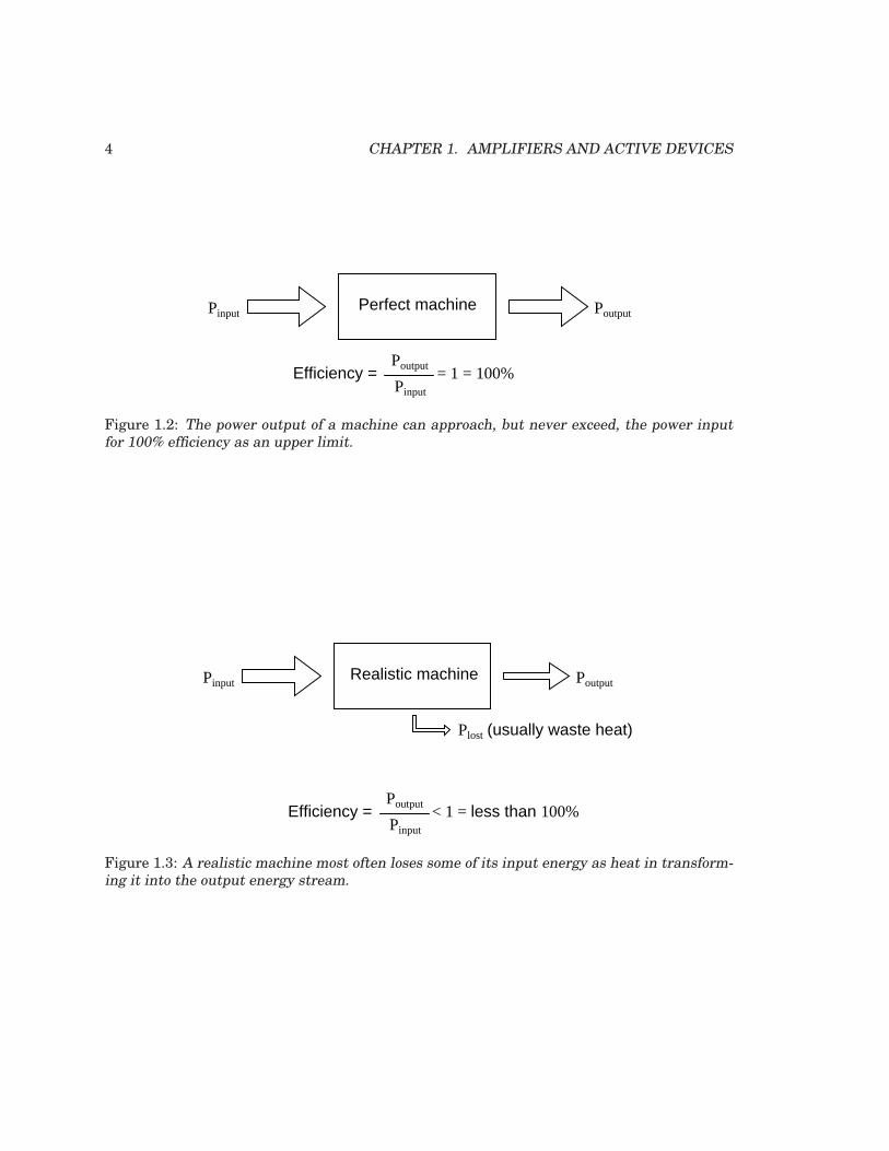
It is a fundamental rule of physics that energy can neither be created nor destroyed. Statedformally, this rule is known as the Law of Conservation of Energy, and no exceptions to it havebeen discovered to date. If this Law is true – and an overwhelming mass of experimental datasuggests that it is – then it is impossible to build a device capable of taking a small amount ofenergy and magically transforming it into a large amount of energy. All machines, electric andelectronic circuits included, have an upper efficiency limit of 100 percent. At best, power outequals power in as in Figure 1.2.
Usually, machines fail even to meet this limit, losing some of their input energy in the formof heat which is radiated into surrounding space and therefore not part of the output energystream. (Figure 1.3)
Many people have attempted, without success, to design and build machines that outputmore power than they take in. Not only would such a perpetual motion machine prove that the
4 CHAPTER 1. AMPLIFIERS AND ACTIVE DEVICES
Perfect machinePinput Poutput
Efficiency = Poutput
Pinput
= 1 = 100%
Figure 1.2: The power output of a machine can approach, but never exceed, the power inputfor 100% efficiency as an upper limit.
Pinput Poutput
Efficiency = Poutput
Pinput
< 1 = less than 100%
Realistic machine
Plost (usually waste heat)
Figure 1.3: A realistic machine most often loses some of its input energy as heat in transform-ing it into the output energy stream.
1.3. AMPLIFIERS 5
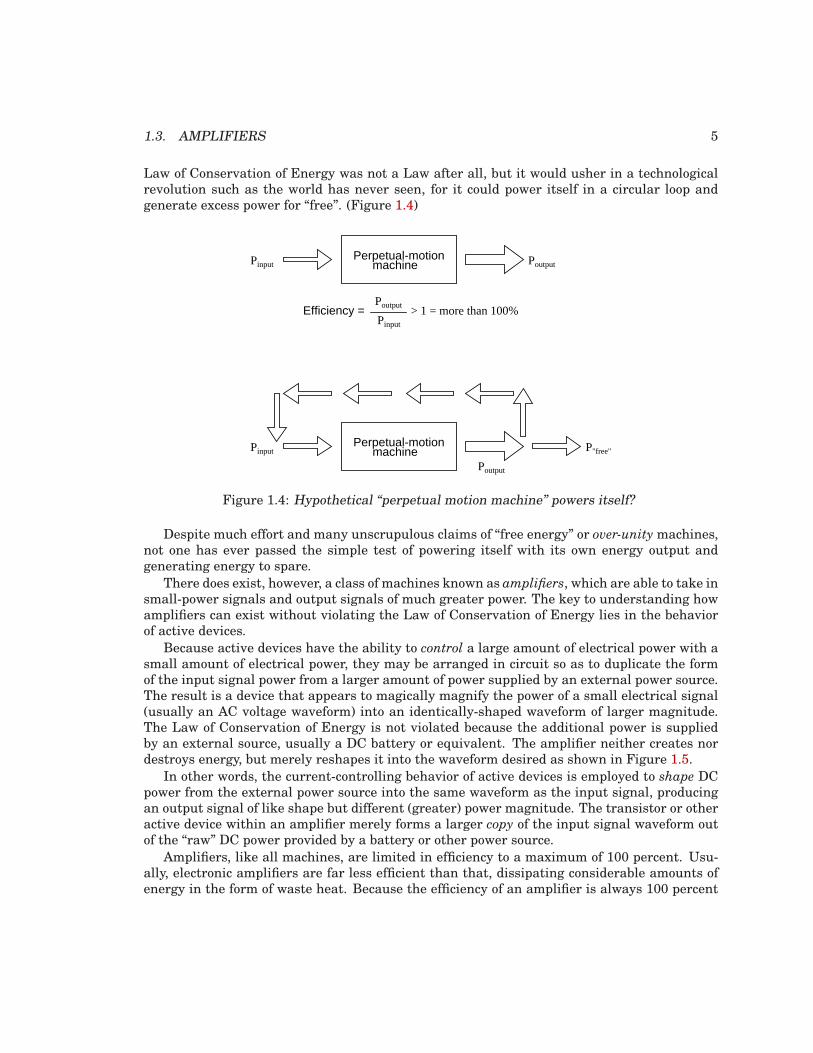
Law of Conservation of Energy was not a Law after all, but it would usher in a technologicalrevolution such as the world has never seen, for it could power itself in a circular loop andgenerate excess power for “free”. (Figure 1.4)
Pinput Poutput
Efficiency = Poutput
Pinput
Perpetual-motionmachine
> 1 = more than 100%
Pinput machinePerpetual-motion
Poutput
P"free"
Figure 1.4: Hypothetical “perpetual motion machine” powers itself?
Despite much effort and many unscrupulous claims of “free energy” or over-unity machines,not one has ever passed the simple test of powering itself with its own energy output andgenerating energy to spare.
There does exist, however, a class of machines known as amplifiers, which are able to take insmall-power signals and output signals of much greater power. The key to understanding howamplifiers can exist without violating the Law of Conservation of Energy lies in the behaviorof active devices.
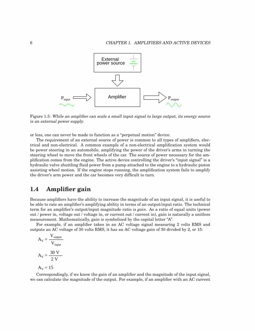
Because active devices have the ability to control a large amount of electrical power with asmall amount of electrical power, they may be arranged in circuit so as to duplicate the formof the input signal power from a larger amount of power supplied by an external power source.The result is a device that appears to magically magnify the power of a small electrical signal(usually an AC voltage waveform) into an identically-shaped waveform of larger magnitude.The Law of Conservation of Energy is not violated because the additional power is suppliedby an external source, usually a DC battery or equivalent. The amplifier neither creates nordestroys energy, but merely reshapes it into the waveform desired as shown in Figure 1.5.
In other words, the current-controlling behavior of active devices is employed to shape DCpower from the external power source into the same waveform as the input signal, producingan output signal of like shape but different (greater) power magnitude. The transistor or otheractive device within an amplifier merely forms a larger copy of the input signal waveform outof the “raw” DC power provided by a battery or other power source.
Amplifiers, like all machines, are limited in efficiency to a maximum of 100 percent. Usu-ally, electronic amplifiers are far less efficient than that, dissipating considerable amounts ofenergy in the form of waste heat. Because the efficiency of an amplifier is always 100 percent
6 CHAPTER 1. AMPLIFIERS AND ACTIVE DEVICES
Pinput PoutputAmplifier
Externalpower source
Figure 1.5: While an amplifier can scale a small input signal to large output, its energy sourceis an external power supply.
or less, one can never be made to function as a “perpetual motion” device.The requirement of an external source of power is common to all types of amplifiers, elec-
trical and non-electrical. A common example of a non-electrical amplification system wouldbe power steering in an automobile, amplifying the power of the driver’s arms in turning thesteering wheel to move the front wheels of the car. The source of power necessary for the am-plification comes from the engine. The active device controlling the driver’s “input signal” is ahydraulic valve shuttling fluid power from a pump attached to the engine to a hydraulic pistonassisting wheel motion. If the engine stops running, the amplification system fails to amplifythe driver’s arm power and the car becomes very difficult to turn.
1.4 Amplifier gain
Because amplifiers have the ability to increase the magnitude of an input signal, it is useful tobe able to rate an amplifier’s amplifying ability in terms of an output/input ratio. The technicalterm for an amplifier’s output/input magnitude ratio is gain. As a ratio of equal units (powerout / power in, voltage out / voltage in, or current out / current in), gain is naturally a unitlessmeasurement. Mathematically, gain is symbolized by the capital letter “A”.
For example, if an amplifier takes in an AC voltage signal measuring 2 volts RMS andoutputs an AC voltage of 30 volts RMS, it has an AC voltage gain of 30 divided by 2, or 15:
AV = Voutput
Vinput
AV = 30 V
2 V
AV = 15
Correspondingly, if we know the gain of an amplifier and the magnitude of the input signal,we can calculate the magnitude of the output. For example, if an amplifier with an AC current
1.4. AMPLIFIER GAIN 7
gain of 3.5 is given an AC input signal of 28 mA RMS, the output will be 3.5 times 28 mA, or98 mA:
Ioutput = (AI)(Iinput)
Ioutput = (3.5)(28 mA)
Ioutput = 98 mA
In the last two examples I specifically identified the gains and signal magnitudes in termsof “AC.” This was intentional, and illustrates an important concept: electronic amplifiers oftenrespond differently to AC and DC input signals, and may amplify them to different extents.Another way of saying this is that amplifiers often amplify changes or variations in inputsignal magnitude (AC) at a different ratio than steady input signal magnitudes (DC). Thespecific reasons for this are too complex to explain at this time, but the fact of the matter isworth mentioning. If gain calculations are to be carried out, it must first be understood whattype of signals and gains are being dealt with, AC or DC.
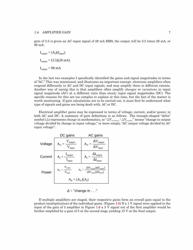
Electrical amplifier gains may be expressed in terms of voltage, current, and/or power, inboth AC and DC. A summary of gain definitions is as follows. The triangle-shaped “delta”symbol (∆) represents change in mathematics, so “∆Voutput / ∆Vinput” means “change in outputvoltage divided by change in input voltage,” or more simply, “AC output voltage divided by ACinput voltage”:
DC gains AC gains
Voltage
Current
Power
AV = Voutput
Vinput
AV = ∆Voutput
∆Vinput
AI =Ioutput
Iinput
AI = ∆Ioutput
∆Iinput
AP = Poutput
Pinput
AP =(∆Voutput)(∆Ioutput)
(∆Vinput)(∆Iinput)
AP = (AV)(AI)
∆ = "change in . . ."
If multiple amplifiers are staged, their respective gains form an overall gain equal to theproduct (multiplication) of the individual gains. (Figure 1.6) If a 1 V signal were applied to theinput of the gain of 3 amplifier in Figure 1.6 a 3 V signal out of the first amplifier would befurther amplified by a gain of 5 at the second stage yielding 15 V at the final output.
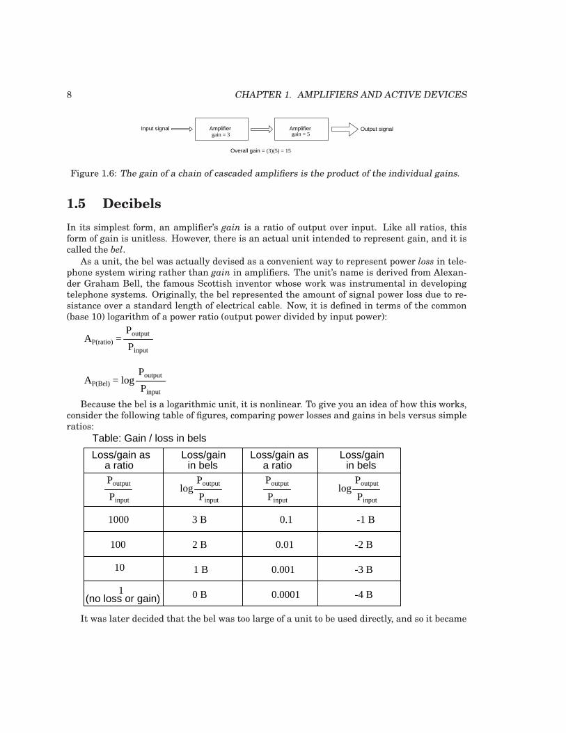
8 CHAPTER 1. AMPLIFIERS AND ACTIVE DEVICES
Amplifiergain = 3
Input signal Output signalAmplifiergain = 5
Overall gain = (3)(5) = 15
Figure 1.6: The gain of a chain of cascaded amplifiers is the product of the individual gains.
1.5 Decibels
In its simplest form, an amplifier’s gain is a ratio of output over input. Like all ratios, thisform of gain is unitless. However, there is an actual unit intended to represent gain, and it iscalled the bel.
As a unit, the bel was actually devised as a convenient way to represent power loss in tele-phone system wiring rather than gain in amplifiers. The unit’s name is derived from Alexan-der Graham Bell, the famous Scottish inventor whose work was instrumental in developingtelephone systems. Originally, the bel represented the amount of signal power loss due to re-sistance over a standard length of electrical cable. Now, it is defined in terms of the common(base 10) logarithm of a power ratio (output power divided by input power):
AP(ratio) = Poutput
Pinput
AP(Bel) = logPoutput
Pinput
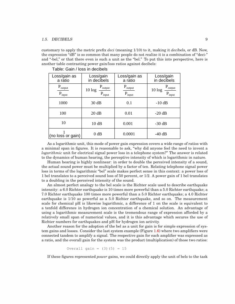
Because the bel is a logarithmic unit, it is nonlinear. To give you an idea of how this works,consider the following table of figures, comparing power losses and gains in bels versus simpleratios:
Loss/gain asa ratio
Loss/gainin bels
1(no loss or gain)
Poutput
Pinput
Poutput
Pinput
log
10
100
1000 3 B
2 B
1 B
0 B
0.1 -1 B
0.01 -2 B
0.001 -3 B
Loss/gain asa ratio
Loss/gainin bels
Poutput
Pinput
Poutput
Pinput
log
Table: Gain / loss in bels
0.0001 -4 B
It was later decided that the bel was too large of a unit to be used directly, and so it became
1.5. DECIBELS 9
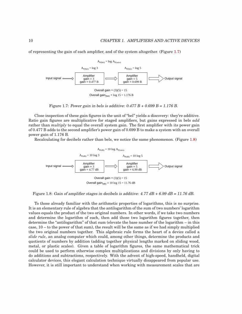
customary to apply the metric prefix deci (meaning 1/10) to it, making it decibels, or dB. Now,the expression “dB” is so common that many people do not realize it is a combination of “deci-”and “-bel,” or that there even is such a unit as the “bel.” To put this into perspective, here isanother table contrasting power gain/loss ratios against decibels:
Loss/gain asa ratio
Loss/gain
1(no loss or gain)
Poutput
Pinput
Poutput
Pinput
10
100
1000
10 log
30 dB
20 dB
10 dB
0 dB
in decibels
0.1
0.01
0.001
-10 dB
-20 dB
-30 dB
Loss/gain asa ratio
Loss/gain
Poutput
Pinput
Poutput
Pinput
10 log
in decibels
0.0001 -40 dB
Table: Gain / loss in decibels
As a logarithmic unit, this mode of power gain expression covers a wide range of ratios witha minimal span in figures. It is reasonable to ask, “why did anyone feel the need to invent alogarithmic unit for electrical signal power loss in a telephone system?” The answer is relatedto the dynamics of human hearing, the perceptive intensity of which is logarithmic in nature.
Human hearing is highly nonlinear: in order to double the perceived intensity of a sound,the actual sound power must be multiplied by a factor of ten. Relating telephone signal powerloss in terms of the logarithmic “bel” scale makes perfect sense in this context: a power loss of1 bel translates to a perceived sound loss of 50 percent, or 1/2. A power gain of 1 bel translatesto a doubling in the perceived intensity of the sound.
An almost perfect analogy to the bel scale is the Richter scale used to describe earthquakeintensity: a 6.0 Richter earthquake is 10 times more powerful than a 5.0 Richter earthquake; a7.0 Richter earthquake 100 times more powerful than a 5.0 Richter earthquake; a 4.0 Richterearthquake is 1/10 as powerful as a 5.0 Richter earthquake, and so on. The measurementscale for chemical pH is likewise logarithmic, a difference of 1 on the scale is equivalent toa tenfold difference in hydrogen ion concentration of a chemical solution. An advantage ofusing a logarithmic measurement scale is the tremendous range of expression afforded by arelatively small span of numerical values, and it is this advantage which secures the use ofRichter numbers for earthquakes and pH for hydrogen ion activity.
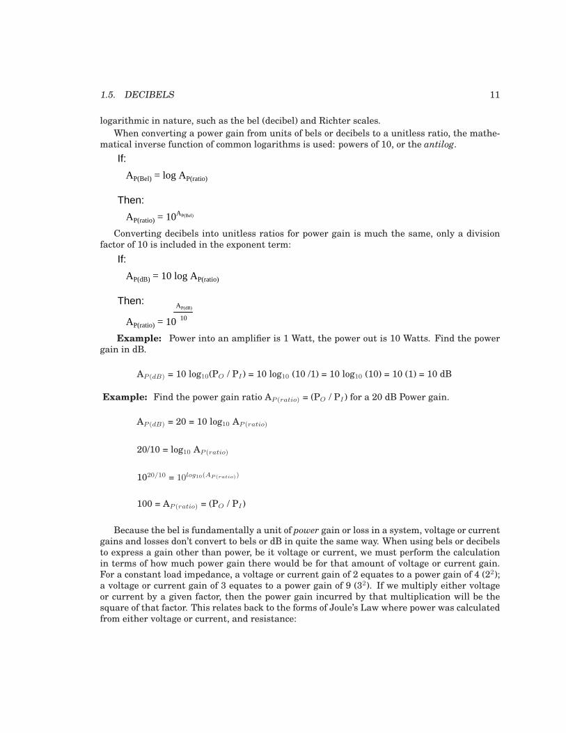
Another reason for the adoption of the bel as a unit for gain is for simple expression of sys-tem gains and losses. Consider the last system example (Figure 1.6) where two amplifiers wereconnected tandem to amplify a signal. The respective gain for each amplifier was expressed asa ratio, and the overall gain for the system was the product (multiplication) of those two ratios:
Overall gain = (3)(5) = 15
If these figures represented power gains, we could directly apply the unit of bels to the task
10 CHAPTER 1. AMPLIFIERS AND ACTIVE DEVICES
of representing the gain of each amplifier, and of the system altogether. (Figure 1.7)
AmplifierInput signal Output signal
Amplifier
Overall gain = (3)(5) = 15
AP(Bel) = log AP(ratio)
AP(Bel) = log 3 AP(Bel) = log 5
gain = 3 gain = 5gain = 0.477 B gain = 0.699 B
Overall gain(Bel) = log 15 = 1.176 B
Figure 1.7: Power gain in bels is additive: 0.477 B + 0.699 B = 1.176 B.
Close inspection of these gain figures in the unit of “bel” yields a discovery: they’re additive.Ratio gain figures are multiplicative for staged amplifiers, but gains expressed in bels add
rather than multiply to equal the overall system gain. The first amplifier with its power gainof 0.477 B adds to the second amplifier’s power gain of 0.699 B to make a system with an overallpower gain of 1.176 B.
Recalculating for decibels rather than bels, we notice the same phenomenon. (Figure 1.8)
AmplifierInput signal Output signal
Amplifier
Overall gain = (3)(5) = 15
gain = 3 gain = 5
AP(dB) = 10 log AP(ratio)
AP(dB) = 10 log 3 AP(dB) = 10 log 5
gain = 4.77 dB gain = 6.99 dB
Overall gain(dB) = 10 log 15 = 11.76 dB
Figure 1.8: Gain of amplifier stages in decibels is additive: 4.77 dB + 6.99 dB = 11.76 dB.
To those already familiar with the arithmetic properties of logarithms, this is no surprise.It is an elementary rule of algebra that the antilogarithm of the sum of two numbers’ logarithmvalues equals the product of the two original numbers. In other words, if we take two numbersand determine the logarithm of each, then add those two logarithm figures together, thendetermine the “antilogarithm” of that sum (elevate the base number of the logarithm – in thiscase, 10 – to the power of that sum), the result will be the same as if we had simply multipliedthe two original numbers together. This algebraic rule forms the heart of a device called aslide rule, an analog computer which could, among other things, determine the products andquotients of numbers by addition (adding together physical lengths marked on sliding wood,metal, or plastic scales). Given a table of logarithm figures, the same mathematical trickcould be used to perform otherwise complex multiplications and divisions by only having todo additions and subtractions, respectively. With the advent of high-speed, handheld, digitalcalculator devices, this elegant calculation technique virtually disappeared from popular use.However, it is still important to understand when working with measurement scales that are
1.5. DECIBELS 11
logarithmic in nature, such as the bel (decibel) and Richter scales.
When converting a power gain from units of bels or decibels to a unitless ratio, the mathe-matical inverse function of common logarithms is used: powers of 10, or the antilog.
If:
AP(Bel) = log AP(ratio)
Then:
AP(ratio) = 10AP(Bel)
Converting decibels into unitless ratios for power gain is much the same, only a divisionfactor of 10 is included in the exponent term:
If:
Then:
AP(dB) = 10 log AP(ratio)
AP(ratio) = 10
AP(dB)
10
Example: Power into an amplifier is 1 Watt, the power out is 10 Watts. Find the powergain in dB.
AP (dB) = 10 log10(PO / PI ) = 10 log10 (10 /1) = 10 log10 (10) = 10 (1) = 10 dB
Example: Find the power gain ratio AP (ratio) = (PO / PI ) for a 20 dB Power gain.
AP (dB) = 20 = 10 log10 AP (ratio)
20/10 = log10 AP (ratio)
1020/10 = 10log10(AP (ratio))
100 = AP (ratio) = (PO / PI )
Because the bel is fundamentally a unit of power gain or loss in a system, voltage or currentgains and losses don’t convert to bels or dB in quite the same way. When using bels or decibelsto express a gain other than power, be it voltage or current, we must perform the calculationin terms of how much power gain there would be for that amount of voltage or current gain.For a constant load impedance, a voltage or current gain of 2 equates to a power gain of 4 (22);a voltage or current gain of 3 equates to a power gain of 9 (32). If we multiply either voltageor current by a given factor, then the power gain incurred by that multiplication will be thesquare of that factor. This relates back to the forms of Joule’s Law where power was calculatedfrom either voltage or current, and resistance:
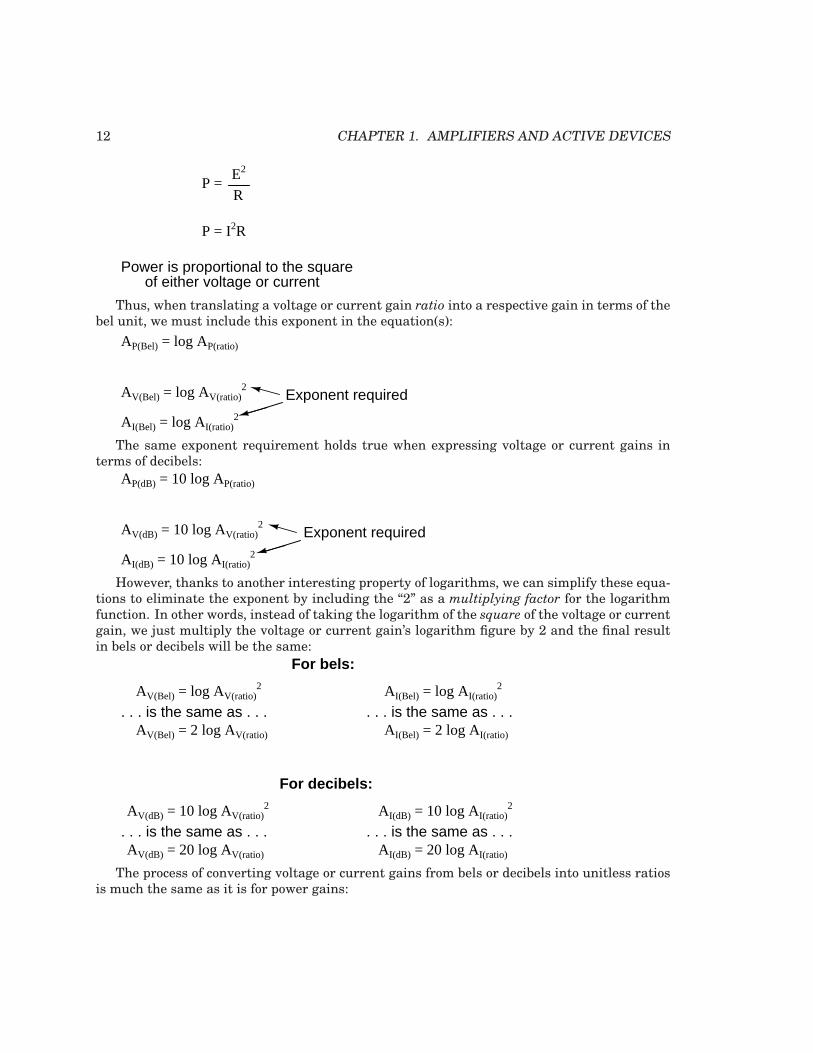
12 CHAPTER 1. AMPLIFIERS AND ACTIVE DEVICES
P = I2R
P =E2
R
Power is proportional to the squareof either voltage or current
Thus, when translating a voltage or current gain ratio into a respective gain in terms of thebel unit, we must include this exponent in the equation(s):
Exponent required
AP(Bel) = log AP(ratio)
AV(Bel) = log AV(ratio)2
AI(Bel) = log AI(ratio)2
The same exponent requirement holds true when expressing voltage or current gains interms of decibels:
Exponent required
AP(dB) = 10 log AP(ratio)
AV(dB) = 10 log AV(ratio)2
AI(dB) = 10 log AI(ratio)2
However, thanks to another interesting property of logarithms, we can simplify these equa-tions to eliminate the exponent by including the “2” as a multiplying factor for the logarithmfunction. In other words, instead of taking the logarithm of the square of the voltage or currentgain, we just multiply the voltage or current gain’s logarithm figure by 2 and the final resultin bels or decibels will be the same:
AI(dB) = 10 log AI(ratio)2
. . . is the same as . . .AV(Bel) = log AV(ratio)
2
AV(Bel) = 2 log AV(ratio)
AI(Bel) = log AI(ratio)2
. . . is the same as . . .AI(Bel) = 2 log AI(ratio)
For bels:
For decibels:
. . . is the same as . . . . . . is the same as . . .AI(dB) = 20 log AI(ratio)
AV(dB) = 10 log AV(ratio)2
AV(dB) = 20 log AV(ratio)
The process of converting voltage or current gains from bels or decibels into unitless ratiosis much the same as it is for power gains:
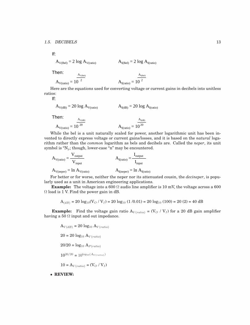
1.5. DECIBELS 13
If:
Then:
AV(Bel) = 2 log AV(ratio)
AV(ratio) = 10 2
AV(Bel)
AI(Bel) = 2 log AI(ratio)
AI(ratio) = 10
AI(Bel)
2
Here are the equations used for converting voltage or current gains in decibels into unitlessratios:
If:
Then:
AV(dB) = 20 log AV(ratio)
AV(ratio) = 10
AV(dB)
20 20
AI(dB) = 20 log AI(ratio)
AI(ratio) = 10
AI(dB)
While the bel is a unit naturally scaled for power, another logarithmic unit has been in-vented to directly express voltage or current gains/losses, and it is based on the natural loga-rithm rather than the common logarithm as bels and decibels are. Called the neper, its unitsymbol is “Np; though, lower-case “n” may be encountered.
AV(neper) = ln AV(ratio)
AV(ratio) = Voutput
Vinput
AI(ratio) =Ioutput
Iinput
AI(neper) = ln AI(ratio)
For better or for worse, neither the neper nor its attenuated cousin, the decineper, is popu-larly used as a unit in American engineering applications.
Example: The voltage into a 600 Ω audio line amplifier is 10 mV, the voltage across a 600Ω load is 1 V. Find the power gain in dB.
A(dB) = 20 log10(VO / VI ) = 20 log10 (1 /0.01) = 20 log10 (100) = 20 (2) = 40 dB
Example: Find the voltage gain ratio AV (ratio) = (VO / VI ) for a 20 dB gain amplifierhaving a 50 Ω input and out impedance.
AV (dB) = 20 log10 AV (ratio)
20 = 20 log10 AV (ratio)
20/20 = log10 AP (ratio)
1020/20 = 10log10(AV (ratio))
10 = AV (ratio) = (VO / VI )
• REVIEW:
14 CHAPTER 1. AMPLIFIERS AND ACTIVE DEVICES
• Gains and losses may be expressed in terms of a unitless ratio, or in the unit of bels (B)or decibels (dB). A decibel is literally a deci-bel: one-tenth of a bel.
• The bel is fundamentally a unit for expressing power gain or loss. To convert a powerratio to either bels or decibels, use one of these equations:
• AP(Bel) = log AP(ratio) AP(db) = 10 log AP(ratio)
• When using the unit of the bel or decibel to express a voltage or current ratio, it must becast in terms of an equivalent power ratio. Practically, this means the use of differentequations, with a multiplication factor of 2 for the logarithm value corresponding to anexponent of 2 for the voltage or current gain ratio:
•
AV(Bel) = 2 log AV(ratio) AV(dB) = 20 log AV(ratio)
AI(Bel) = 2 log AI(ratio) AI(dB) = 20 log AI(ratio)
• To convert a decibel gain into a unitless ratio gain, use one of these equations:
•
AV(ratio) = 10
AV(dB)
20
20AI(ratio) = 10
AI(dB)
AP(ratio) = 10
AP(dB)
10
• A gain (amplification) is expressed as a positive bel or decibel figure. A loss (attenuation)is expressed as a negative bel or decibel figure. Unity gain (no gain or loss; ratio = 1) isexpressed as zero bels or zero decibels.
• When calculating overall gain for an amplifier system composed of multiple amplifierstages, individual gain ratios are multiplied to find the overall gain ratio. Bel or deci-bel figures for each amplifier stage, on the other hand, are added together to determineoverall gain.
1.6 Absolute dB scales
It is also possible to use the decibel as a unit of absolute power, in addition to using it as anexpression of power gain or loss. A common example of this is the use of decibels as a measure-ment of sound pressure intensity. In cases like these, the measurement is made in reference tosome standardized power level defined as 0 dB. For measurements of sound pressure, 0 dB isloosely defined as the lower threshold of human hearing, objectively quantified as 1 picowattof sound power per square meter of area.
A sound measuring 40 dB on the decibel sound scale would be 104 times greater than thethreshold of hearing. A 100 dB sound would be 1010 (ten billion) times greater than the thresh-old of hearing.
1.6. ABSOLUTE DB SCALES 15
Because the human ear is not equally sensitive to all frequencies of sound, variations of thedecibel sound-power scale have been developed to represent physiologically equivalent soundintensities at different frequencies. Some sound intensity instruments were equipped withfilter networks to give disproportionate indications across the frequency scale, the intent ofwhich to better represent the effects of sound on the human body. Three filtered scales becamecommonly known as the “A,” “B,” and “C” weighted scales. Decibel sound intensity indicationsmeasured through these respective filtering networks were given in units of dBA, dBB, anddBC. Today, the “A-weighted scale” is most commonly used for expressing the equivalent phys-iological impact on the human body, and is especially useful for rating dangerously loud noisesources.
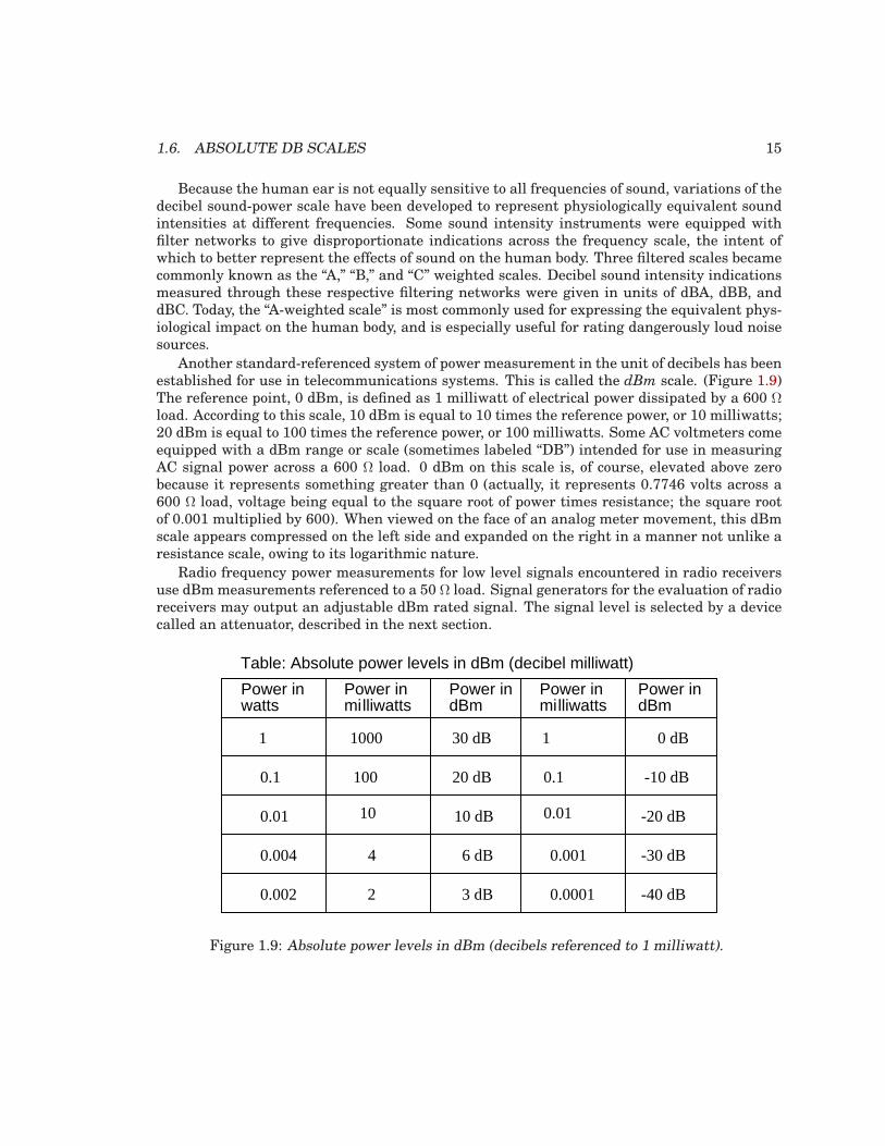
Another standard-referenced system of power measurement in the unit of decibels has beenestablished for use in telecommunications systems. This is called the dBm scale. (Figure 1.9)The reference point, 0 dBm, is defined as 1 milliwatt of electrical power dissipated by a 600 Ωload. According to this scale, 10 dBm is equal to 10 times the reference power, or 10 milliwatts;20 dBm is equal to 100 times the reference power, or 100 milliwatts. Some AC voltmeters comeequipped with a dBm range or scale (sometimes labeled “DB”) intended for use in measuringAC signal power across a 600 Ω load. 0 dBm on this scale is, of course, elevated above zerobecause it represents something greater than 0 (actually, it represents 0.7746 volts across a600 Ω load, voltage being equal to the square root of power times resistance; the square rootof 0.001 multiplied by 600). When viewed on the face of an analog meter movement, this dBmscale appears compressed on the left side and expanded on the right in a manner not unlike aresistance scale, owing to its logarithmic nature.
Radio frequency power measurements for low level signals encountered in radio receiversuse dBmmeasurements referenced to a 50 Ω load. Signal generators for the evaluation of radioreceivers may output an adjustable dBm rated signal. The signal level is selected by a devicecalled an attenuator, described in the next section.
Power inwatts
0.1
0.01
-10 dB
-20 dB
Table: Absolute power levels in dBm (decibel milliwatt)
Power inmilliwatts
Power indBm
30 dB
20 dB
10 dB
0 dB1
10
100
10001
0.002 3 dB2
Power inmilliwatts
0.01
0.1
Power indBm
-30 dB0.004 6 dB4 0.001
-40 dB0.0001
Figure 1.9: Absolute power levels in dBm (decibels referenced to 1 milliwatt).
16 CHAPTER 1. AMPLIFIERS AND ACTIVE DEVICES
An adaptation of the dBm scale for audio signal strength is used in studio recording andbroadcast engineering for standardizing volume levels, and is called the VU scale. VU metersare frequently seen on electronic recording instruments to indicate whether or not the recordedsignal exceeds the maximum signal level limit of the device, where significant distortion willoccur. This “volume indicator” scale is calibrated in according to the dBm scale, but does notdirectly indicate dBm for any signal other than steady sine-wave tones. The proper unit ofmeasurement for a VU meter is volume units.
When relatively large signals are dealt with, and an absolute dB scale would be useful forrepresenting signal level, specialized decibel scales are sometimes used with reference pointsgreater than the 1 mW used in dBm. Such is the case for the dBW scale, with a referencepoint of 0 dBW established at 1 Watt. Another absolute measure of power called the dBk scalereferences 0 dBk at 1 kW, or 1000 Watts.
• REVIEW:
• The unit of the bel or decibel may also be used to represent an absolute measurement ofpower rather than just a relative gain or loss. For sound power measurements, 0 dB isdefined as a standardized reference point of power equal to 1 picowatt per square meter.Another dB scale suited for sound intensity measurements is normalized to the samephysiological effects as a 1000 Hz tone, and is called the dBA scale. In this system, 0dBA is defined as any frequency sound having the same physiological equivalence as a 1picowatt-per-square-meter tone at 1000 Hz.
• An electrical dB scale with an absolute reference point has been made for use in telecom-munications systems. Called the dBm scale, its reference point of 0 dBm is defined as 1milliwatt of AC signal power dissipated by a 600 Ω load.
• A VU meter reads audio signal level according to the dBm for sine-wave signals. Becauseits response to signals other than steady sine waves is not the same as true dBm, its unitof measurement is volume units.
• dB scales with greater absolute reference points than the dBm scale have been inventedfor high-power signals. The dBW scale has its reference point of 0 dBW defined as 1 Wattof power. The dBk scale sets 1 kW (1000 Watts) as the zero-point reference.
1.7 Attenuators
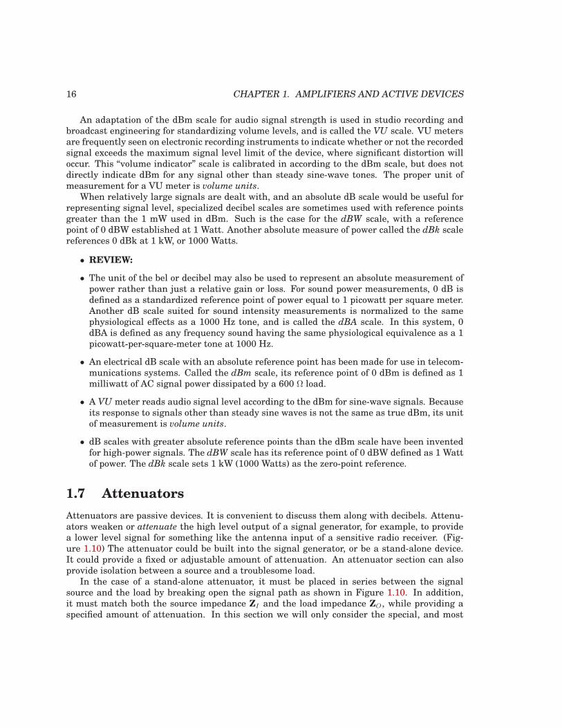
Attenuators are passive devices. It is convenient to discuss them along with decibels. Attenu-ators weaken or attenuate the high level output of a signal generator, for example, to providea lower level signal for something like the antenna input of a sensitive radio receiver. (Fig-ure 1.10) The attenuator could be built into the signal generator, or be a stand-alone device.It could provide a fixed or adjustable amount of attenuation. An attenuator section can alsoprovide isolation between a source and a troublesome load.
In the case of a stand-alone attenuator, it must be placed in series between the signalsource and the load by breaking open the signal path as shown in Figure 1.10. In addition,it must match both the source impedance ZI and the load impedance ZO, while providing aspecified amount of attenuation. In this section we will only consider the special, and most
1.7. ATTENUATORS 17
ZO
ZI
Attenuator
ZO
ZI
Figure 1.10: Constant impedance attenuator is matched to source impedance ZI and loadimpedance ZO. For radio frequency equipment Z is 50 Ω.
common, case where the source and load impedances are equal. Not considered in this section,unequal source and load impedances may be matched by an attenuator section. However, theformulation is more complex.
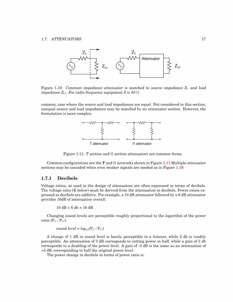
T attenuator Π attenuator
Figure 1.11: T section and Π section attenuators are common forms.
Common configurations are the T and Π networks shown in Figure 1.11 Multiple attenuatorsections may be cascaded when even weaker signals are needed as in Figure 1.19.
1.7.1 Decibels
Voltage ratios, as used in the design of attenuators are often expressed in terms of decibels.The voltage ratio (K below) must be derived from the attenuation in decibels. Power ratios ex-pressed as decibels are additive. For example, a 10 dB attenuator followed by a 6 dB attenuatorprovides 16dB of attenuation overall.
10 dB + 6 db = 16 dB
Changing sound levels are perceptible roughly proportional to the logarithm of the powerratio (PI / PO).
sound level = log10(PI / PO)
A change of 1 dB in sound level is barely perceptible to a listener, while 2 db is readilyperceptible. An attenuation of 3 dB corresponds to cutting power in half, while a gain of 3 dbcorresponds to a doubling of the power level. A gain of -3 dB is the same as an attenuation of+3 dB, corresponding to half the original power level.
The power change in decibels in terms of power ratio is:
18 CHAPTER 1. AMPLIFIERS AND ACTIVE DEVICES
dB = 10 log10(PI / PO)
Assuming that the load RI at PI is the same as the load resistor RO at PO (RI = RO), thedecibels may be derived from the voltage ratio (VI / VO) or current ratio (II / IO):
PO = V O IO = VO2 / R = IO
2 R
PI = VI II = VI2 / R = II
2 R
dB = 10 log10(PI / PO) = 10 log10(VI2 / VO
2) = 20 log10(VI /VO)
dB = 10 log10(PI / PO) = 10 log10(II2 / IO
2) = 20 log10(II /IO)
The two most often used forms of the decibel equation are:
dB = 10 log10(PI / PO) or dB = 20 log10(VI / VO)
We will use the latter form, since we need the voltage ratio. Once again, the voltage ratioform of equation is only applicable where the two corresponding resistors are equal. That is,the source and load resistance need to be equal.
Example: Power into an attenuator is 10 Watts, the power out is 1 Watt. Find theattenuation in dB.
dB = 10 log10(PI / PO) = 10 log10 (10 /1) = 10 log10 (10) = 10 (1) = 10 dB
Example: Find the voltage attenuation ratio (K= (VI / VO)) for a 10 dB attenuator.
dB = 10= 20 log10(VI / VO)
10/20 = log10(VI / VO)
1010/20 = 10log10(VI/VO)
3.16 = (VI / VO) = AP (ratio)
Example: Power into an attenuator is 100 milliwatts, the power out is 1 milliwatt. Findthe attenuation in dB.
dB = 10 log10(PI / PO) = 10 log10 (100 /1) = 10 log10 (100) = 10 (2) = 20 dB
Example: Find the voltage attenuation ratio (K= (VI / VO)) for a 20 dB attenuator.
dB = 20= 20 log10(VI / VO )
1020/20 = 10log10(VI/VO)
10 = (VI / VO ) = K
1.7. ATTENUATORS 19
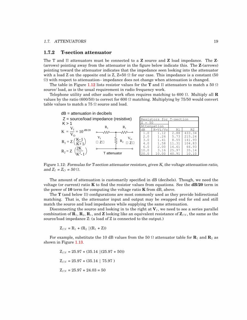
1.7.2 T-section attenuator
The T and Π attenuators must be connected to a Z source and Z load impedance. The Z-(arrows) pointing away from the attenuator in the figure below indicate this. The Z-(arrows)pointing toward the attenuator indicates that the impedance seen looking into the attenuatorwith a load Z on the opposite end is Z, Z=50 Ω for our case. This impedance is a constant (50Ω) with respect to attenuation– impedance does not change when attenuation is changed.
The table in Figure 1.12 lists resistor values for the T and Π attenuators to match a 50 Ωsource/ load, as is the usual requirement in radio frequency work.
Telephone utility and other audio work often requires matching to 600 Ω. Multiply all Rvalues by the ratio (600/50) to correct for 600 Ω matching. Multiplying by 75/50 would converttable values to match a 75 Ω source and load.
R1 = Z
R2 = Z
K-1K+12K
K2-1
dB = attenuation in decibels
K > 1
K = = 10 dB/20
VO
VI
Z = source/load impedance (resistive)
R1 R1
R2⇐Ζ⇒VI VO
⇐Ζ⇒
T attenuator
Resistors for T-section Z = 50 Attenuation dB K=Vi/Vo R1 R2 1.0 1.12 2.88 433.34 2.0 1.26 5.73 215.24 3.0 1.41 8.55 141.93 4.0 1.58 11.31 104.83 6.0 2.00 16.61 66.93 10.0 3.16 25.97 35.14 20.0 10.00 40.91 10.10
Figure 1.12: Formulas for T-section attenuator resistors, given K, the voltage attenuation ratio,and ZI = ZO = 50 Ω.
The amount of attenuation is customarily specified in dB (decibels). Though, we need thevoltage (or current) ratio K to find the resistor values from equations. See the dB/20 term inthe power of 10 term for computing the voltage ratio K from dB, above.
The T (and below Π) configurations are most commonly used as they provide bidirectionalmatching. That is, the attenuator input and output may be swapped end for end and stillmatch the source and load impedances while supplying the same attenuation.
Disconnecting the source and looking in to the right at VI , we need to see a series parallelcombination of R1, R2, R1, and Z looking like an equivalent resistance of ZIN , the same as thesource/load impedance Z: (a load of Z is connected to the output.)
ZIN = R1 + (R2 ||(R1 + Z))
For example, substitute the 10 dB values from the 50 Ω attenuator table for R1 and R2 asshown in Figure 1.13.
ZIN = 25.97 + (35.14 ||(25.97 + 50))
ZIN = 25.97 + (35.14 || 75.97 )
ZIN = 25.97 + 24.03 = 50
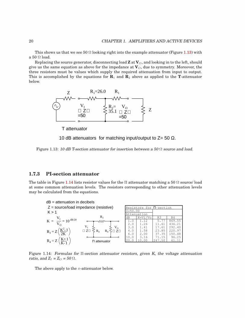
20 CHAPTER 1. AMPLIFIERS AND ACTIVE DEVICES
This shows us that we see 50 Ω looking right into the example attenuator (Figure 1.13) witha 50 Ω load.
Replacing the source generator, disconnecting load Z atVO, and looking in to the left, shouldgive us the same equation as above for the impedance at VO, due to symmetry. Moreover, thethree resistors must be values which supply the required attenuation from input to output.This is accomplished by the equations for R1 and R2 above as applied to the T-attenuatorbelow.
R1=26.0 R1
R2=35.1⇐Ζ⇒
=50
VI VO
T attenuator
⇐Ζ⇒=50
10 dB attenuators for matching input/output to Z= 50 Ω.
Z
Z
Figure 1.13: 10 dB T-section attenuator for insertion between a 50 Ω source and load.
1.7.3 PI-section attenuator
The table in Figure 1.14 lists resistor values for the Π attenuator matching a 50 Ω source/ loadat some common attenuation levels. The resistors corresponding to other attenuation levelsmay be calculated from the equations.
dB = attenuation in decibels
K > 1
K = = 10 dB/20
VO
VI
Z = source/load impedance (resistive)
R4 = Z
R3 = Z
K-1K+ 12KK2-1
R3
R4
VI VO⇐Ζ⇒ ⇐Ζ⇒R4
Π attenuator
Resistors for Π-section Z=50.00 Attenuation dB K=Vi/Vo R3 R4 1.0 1.12 5.77 869.55 2.0 1.26 11.61 436.21 3.0 1.41 17.61 292.40 4.0 1.58 23.85 220.97 6.0 2.00 37.35 150.48 10.0 3.16 71.15 96.25 20.0 10.00 247.50 61.11
Figure 1.14: Formulas for Π-section attenuator resistors, given K, the voltage attenuationratio, and ZI = ZO = 50 Ω.
The above apply to the π-attenuator below.
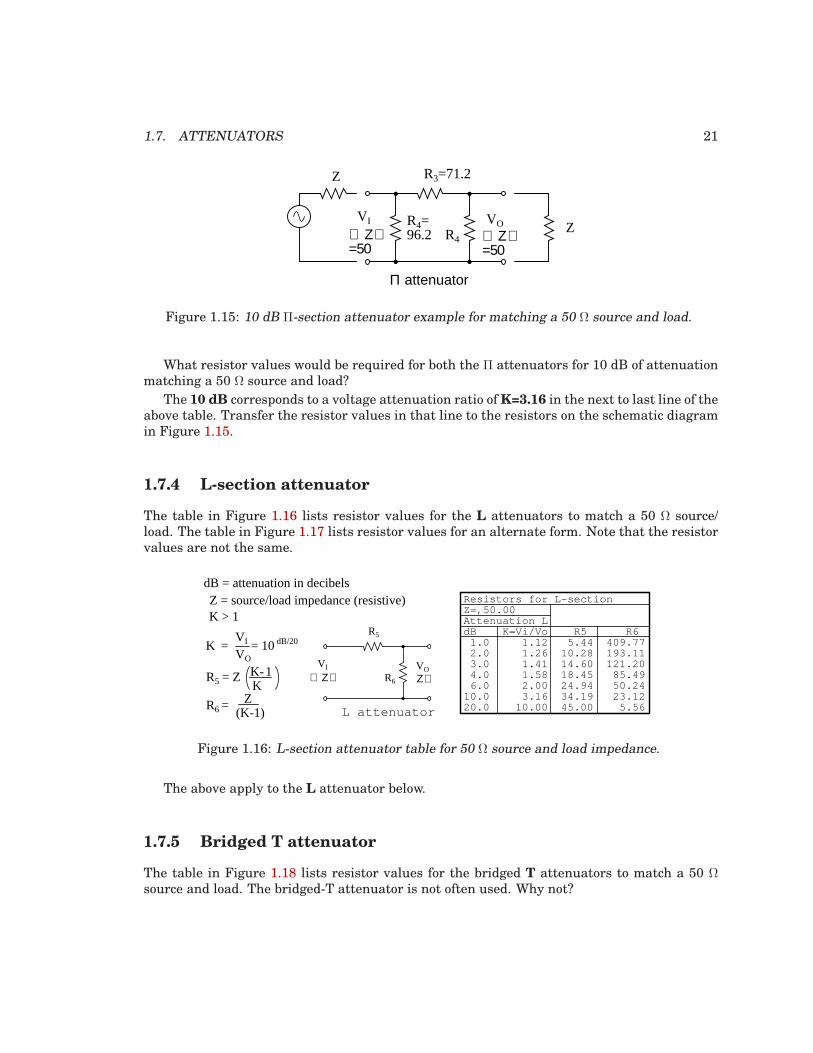
1.7. ATTENUATORS 21
R3=71.2
R4=96.2
VI VOR4
Π attenuator
⇐Ζ⇒=50
⇐Ζ⇒=50
Z
Z
Figure 1.15: 10 dB Π-section attenuator example for matching a 50 Ω source and load.
What resistor values would be required for both the Π attenuators for 10 dB of attenuationmatching a 50 Ω source and load?
The 10 dB corresponds to a voltage attenuation ratio ofK=3.16 in the next to last line of theabove table. Transfer the resistor values in that line to the resistors on the schematic diagramin Figure 1.15.
1.7.4 L-section attenuator
The table in Figure 1.16 lists resistor values for the L attenuators to match a 50 Ω source/load. The table in Figure 1.17 lists resistor values for an alternate form. Note that the resistorvalues are not the same.
dB = attenuation in decibels
K > 1
K = = 10 dB/20
VO
VI
Z = source/load impedance (resistive)
R5 = ZKK-1
R5
VI VO⇐Ζ⇒ Ζ⇒R6
L attenuator
Resistors for L-section Z=,50.00 Attenuation L dB K=Vi/Vo R5 R6 1.0 1.12 5.44 409.77 2.0 1.26 10.28 193.11 3.0 1.41 14.60 121.20 4.0 1.58 18.45 85.49 6.0 2.00 24.94 50.24 10.0 3.16 34.19 23.12 20.0 10.00 45.00 5.56 R6 =
(K-1)Z
Figure 1.16: L-section attenuator table for 50 Ω source and load impedance.
The above apply to the L attenuator below.
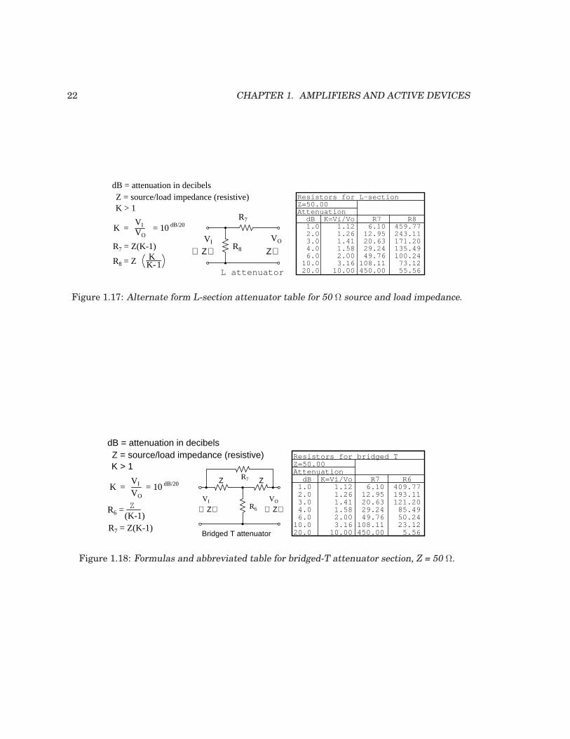
1.7.5 Bridged T attenuator
The table in Figure 1.18 lists resistor values for the bridged T attenuators to match a 50 Ωsource and load. The bridged-T attenuator is not often used. Why not?
22 CHAPTER 1. AMPLIFIERS AND ACTIVE DEVICES
dB = attenuation in decibels
K > 1
K = = 10 dB/20
VO
VI
Z = source/load impedance (resistive)
R8 = Z KK-1
R7
VI VO
⇐Ζ⇒ Ζ⇒R8
L attenuator
Resistors for L-section Z=50.00 Attenuation dB K=Vi/Vo R7 R8 1.0 1.12 6.10 459.77 2.0 1.26 12.95 243.11 3.0 1.41 20.63 171.20 4.0 1.58 29.24 135.49 6.0 2.00 49.76 100.24 10.0 3.16 108.11 73.12 20.0 10.00 450.00 55.56
R7 = Z(K-1)
Figure 1.17: Alternate form L-section attenuator table for 50 Ω source and load impedance.
dB = attenuation in decibels
K > 1
K = = 10 dB/20
VO
VI
Z = source/load impedance (resistive)
R6 = (K-1)Z
R7 = Z(K-1)
Resistors for bridged T Z=50.00 Attenuation dB K=Vi/Vo R7 R6 1.0 1.12 6.10 409.77 2.0 1.26 12.95 193.11 3.0 1.41 20.63 121.20 4.0 1.58 29.24 85.49 6.0 2.00 49.76 50.24 10.0 3.16 108.11 23.12 20.0 10.00 450.00 5.56
R7
R6⇐Ζ⇒VI VO
⇐Ζ⇒
Bridged T attenuator
Ζ Ζ
Figure 1.18: Formulas and abbreviated table for bridged-T attenuator section, Z = 50 Ω.
1.7. ATTENUATORS 23
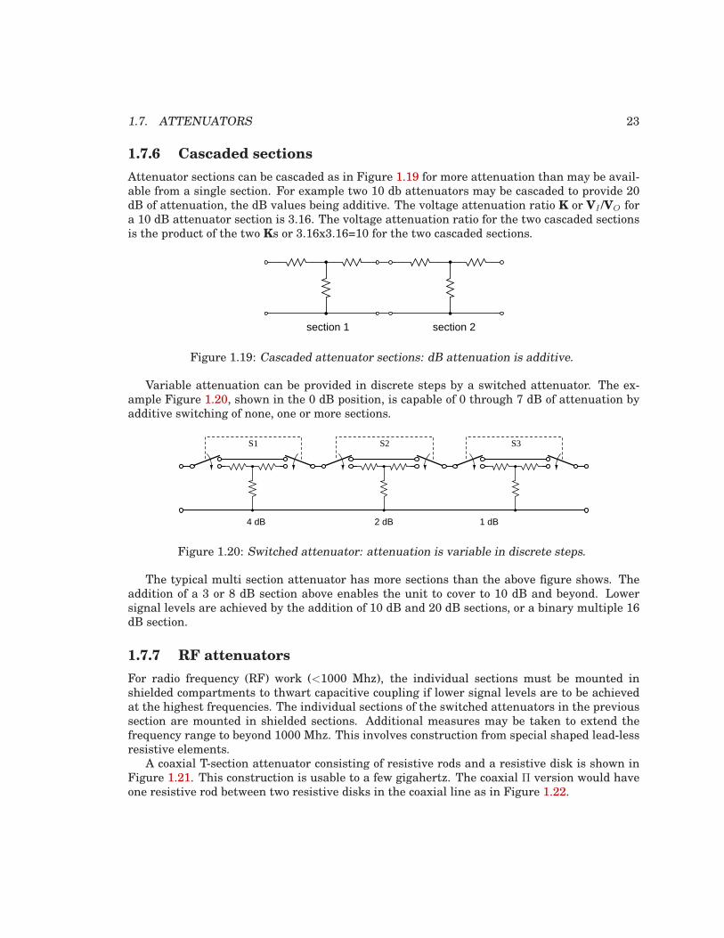
1.7.6 Cascaded sections
Attenuator sections can be cascaded as in Figure 1.19 for more attenuation than may be avail-able from a single section. For example two 10 db attenuators may be cascaded to provide 20dB of attenuation, the dB values being additive. The voltage attenuation ratio K or VI /VO fora 10 dB attenuator section is 3.16. The voltage attenuation ratio for the two cascaded sectionsis the product of the two Ks or 3.16x3.16=10 for the two cascaded sections.
section 1 section 2
Figure 1.19: Cascaded attenuator sections: dB attenuation is additive.
Variable attenuation can be provided in discrete steps by a switched attenuator. The ex-ample Figure 1.20, shown in the 0 dB position, is capable of 0 through 7 dB of attenuation byadditive switching of none, one or more sections.
4 dB 2 dB 1 dB
S1 S2 S3
Figure 1.20: Switched attenuator: attenuation is variable in discrete steps.
The typical multi section attenuator has more sections than the above figure shows. Theaddition of a 3 or 8 dB section above enables the unit to cover to 10 dB and beyond. Lowersignal levels are achieved by the addition of 10 dB and 20 dB sections, or a binary multiple 16dB section.
1.7.7 RF attenuators
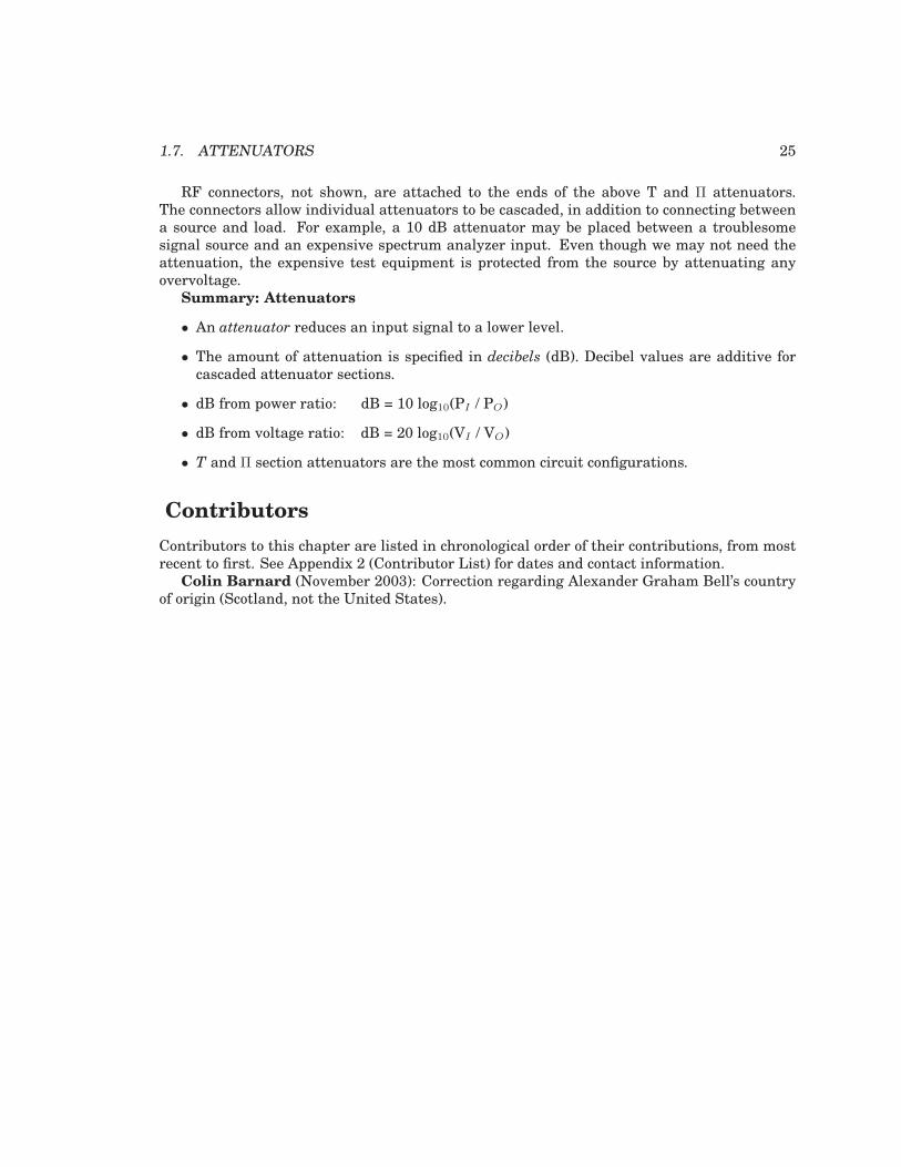
For radio frequency (RF) work (<1000 Mhz), the individual sections must be mounted inshielded compartments to thwart capacitive coupling if lower signal levels are to be achievedat the highest frequencies. The individual sections of the switched attenuators in the previoussection are mounted in shielded sections. Additional measures may be taken to extend thefrequency range to beyond 1000 Mhz. This involves construction from special shaped lead-lessresistive elements.
A coaxial T-section attenuator consisting of resistive rods and a resistive disk is shown inFigure 1.21. This construction is usable to a few gigahertz. The coaxial Π version would haveone resistive rod between two resistive disks in the coaxial line as in Figure 1.22.
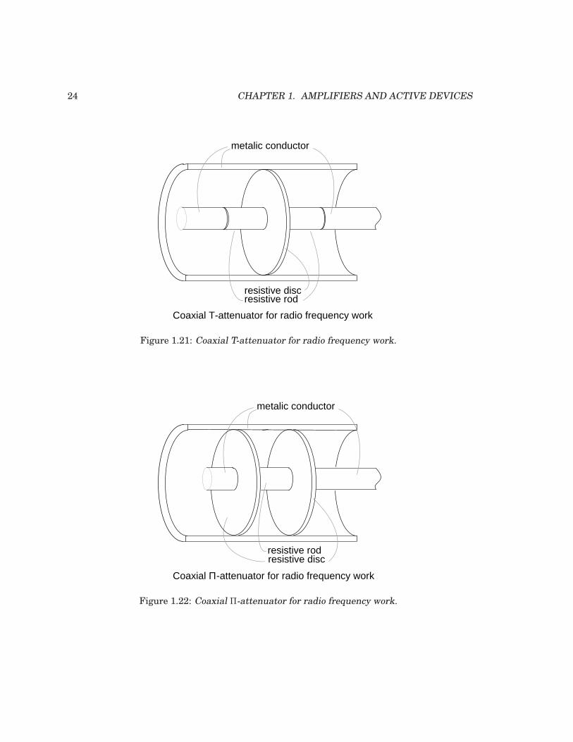
24 CHAPTER 1. AMPLIFIERS AND ACTIVE DEVICES
metalic conductor
resistive rodresistive disc
Coaxial T-attenuator for radio frequency work
Figure 1.21: Coaxial T-attenuator for radio frequency work.
metalic conductor
resistive rodresistive disc
Coaxial Π-attenuator for radio frequency work
Figure 1.22: Coaxial Π-attenuator for radio frequency work.
1.7. ATTENUATORS 25
RF connectors, not shown, are attached to the ends of the above T and Π attenuators.The connectors allow individual attenuators to be cascaded, in addition to connecting betweena source and load. For example, a 10 dB attenuator may be placed between a troublesomesignal source and an expensive spectrum analyzer input. Even though we may not need theattenuation, the expensive test equipment is protected from the source by attenuating anyovervoltage.
Summary: Attenuators
• An attenuator reduces an input signal to a lower level.
• The amount of attenuation is specified in decibels (dB). Decibel values are additive forcascaded attenuator sections.
• dB from power ratio: dB = 10 log10(PI / PO)
• dB from voltage ratio: dB = 20 log10(VI / VO)
• T and Π section attenuators are the most common circuit configurations.
Contributors
Contributors to this chapter are listed in chronological order of their contributions, from mostrecent to first. See Appendix 2 (Contributor List) for dates and contact information.
Colin Barnard (November 2003): Correction regarding Alexander Graham Bell’s countryof origin (Scotland, not the United States).

26 CHAPTER 1. AMPLIFIERS AND ACTIVE DEVICES
Chapter 2
SOLID-STATE DEVICE THEORY
Contents
2.1 Introduction . . . . . . . . . . . . . . . . . . . . . . . . . . . . . . . . . . . . . . 27
2.2 Quantum physics . . . . . . . . . . . . . . . . . . . . . . . . . . . . . . . . . . . 28
2.3 Valence and Crystal structure . . . . . . . . . . . . . . . . . . . . . . . . . . . 41
2.4 Band theory of solids . . . . . . . . . . . . . . . . . . . . . . . . . . . . . . . . 47
2.5 Electrons and “holes” . . . . . . . . . . . . . . . . . . . . . . . . . . . . . . . . 50
2.6 The P-N junction . . . . . . . . . . . . . . . . . . . . . . . . . . . . . . . . . . . 55
2.7 Junction diodes . . . . . . . . . . . . . . . . . . . . . . . . . . . . . . . . . . . . 58
2.8 Bipolar junction transistors . . . . . . . . . . . . . . . . . . . . . . . . . . . . 60
2.9 Junction field-effect transistors . . . . . . . . . . . . . . . . . . . . . . . . . . 65
2.10 Insulated-gate field-effect transistors (MOSFET) . . . . . . . . . . . . . . . 70
2.11 Thyristors . . . . . . . . . . . . . . . . . . . . . . . . . . . . . . . . . . . . . . . 73
2.12 Semiconductor manufacturing techniques . . . . . . . . . . . . . . . . . . . 75
2.13 Superconducting devices . . . . . . . . . . . . . . . . . . . . . . . . . . . . . . 80
2.14 Quantum devices . . . . . . . . . . . . . . . . . . . . . . . . . . . . . . . . . . . 83
2.15 Semiconductor devices in SPICE . . . . . . . . . . . . . . . . . . . . . . . . . 91
Bibliography . . . . . . . . . . . . . . . . . . . . . . . . . . . . . . . . . . . . . . . . . 93
2.1 Introduction
This chapter will cover the physics behind the operation of semiconductor devices and showhow these principles are applied in several different types of semiconductor devices. Subse-quent chapters will deal primarily with the practical aspects of these devices in circuits andomit theory as much as possible.
27
28 CHAPTER 2. SOLID-STATE DEVICE THEORY
2.2 Quantum physics
“I think it is safe to say that no one understands quantum mechanics.”
Physicist Richard P. Feynman
To say that the invention of semiconductor devices was a revolution would not be an ex-aggeration. Not only was this an impressive technological accomplishment, but it paved theway for developments that would indelibly alter modern society. Semiconductor devices madepossible miniaturized electronics, including computers, certain types of medical diagnostic andtreatment equipment, and popular telecommunication devices, to name a few applications ofthis technology.
But behind this revolution in technology stands an even greater revolution in general sci-ence: the field of quantum physics. Without this leap in understanding the natural world, thedevelopment of semiconductor devices (and more advanced electronic devices still under devel-opment) would never have been possible. Quantum physics is an incredibly complicated realmof science. This chapter is but a brief overview. When scientists of Feynman’s caliber say that“no one understands [it],” you can be sure it is a complex subject. Without a basic understand-ing of quantum physics, or at least an understanding of the scientific discoveries that led to itsformulation, though, it is impossible to understand how and why semiconductor electronic de-vices function. Most introductory electronics textbooks I’ve read try to explain semiconductorsin terms of “classical” physics, resulting in more confusion than comprehension.
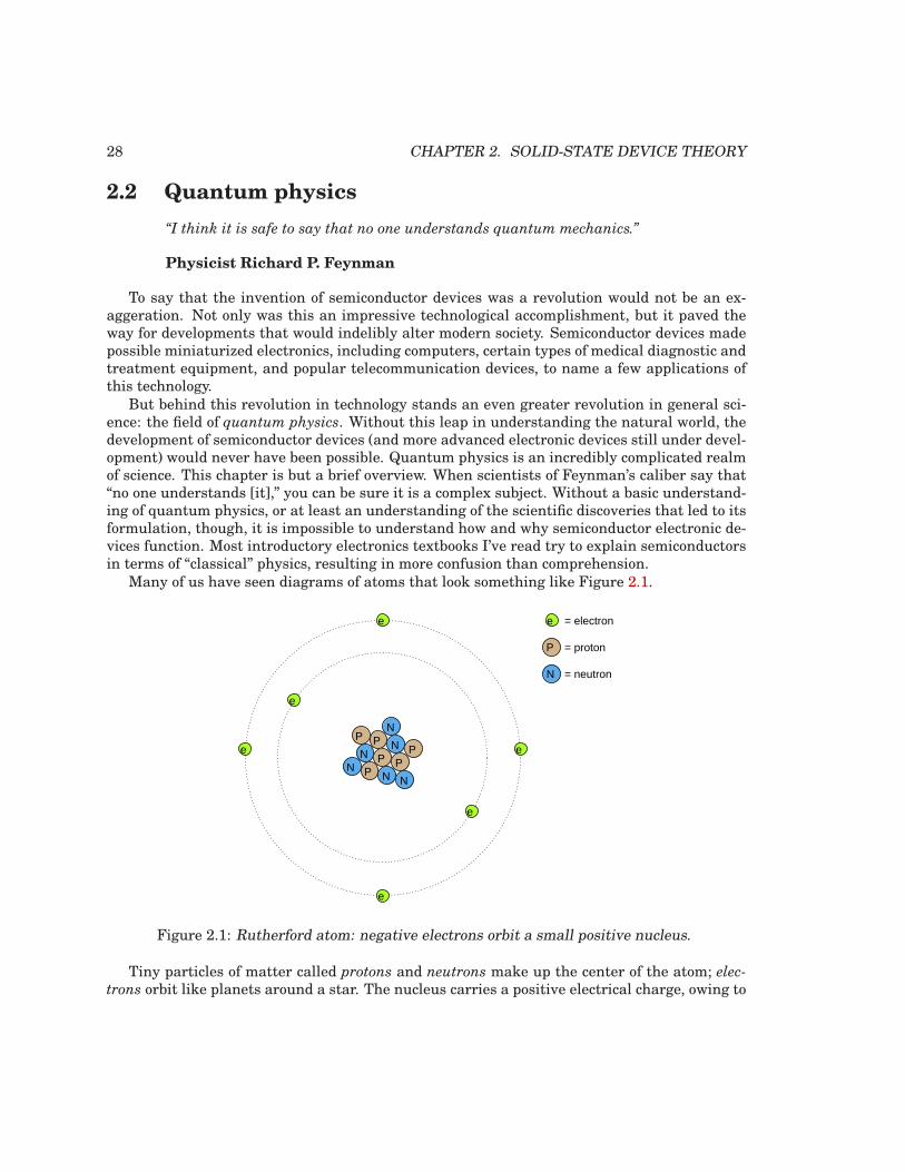
Many of us have seen diagrams of atoms that look something like Figure 2.1.
= electron
= proton
= neutron
e
N
P
P
P
PP
PP
N
N
N N
NN
e
e
ee
e
e
Figure 2.1: Rutherford atom: negative electrons orbit a small positive nucleus.
Tiny particles of matter called protons and neutrons make up the center of the atom; elec-trons orbit like planets around a star. The nucleus carries a positive electrical charge, owing to
2.2. QUANTUM PHYSICS 29
the presence of protons (the neutrons have no electrical charge whatsoever), while the atom’sbalancing negative charge resides in the orbiting electrons. The negative electrons are at-tracted to the positive protons just as planets are gravitationally attracted by the Sun, yet theorbits are stable because of the electrons’ motion. We owe this popular model of the atom to thework of Ernest Rutherford, who around the year 1911 experimentally determined that atoms’positive charges were concentrated in a tiny, dense core rather than being spread evenly aboutthe diameter as was proposed by an earlier researcher, J.J. Thompson.
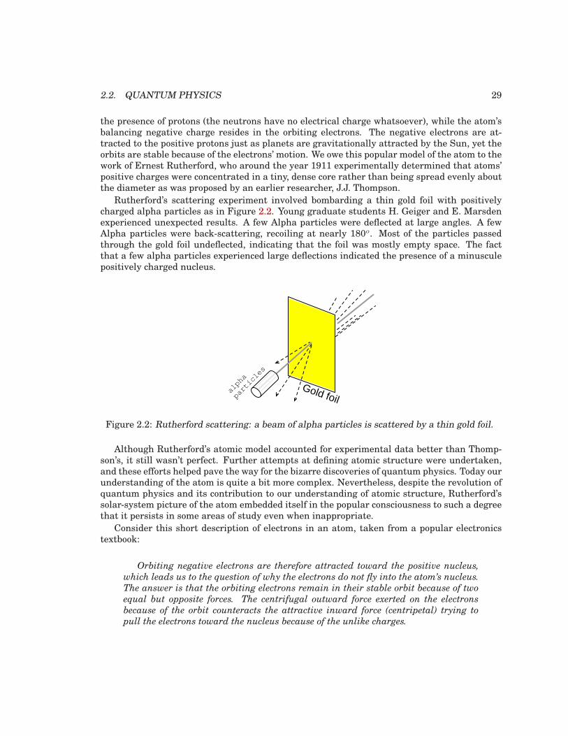
Rutherford’s scattering experiment involved bombarding a thin gold foil with positivelycharged alpha particles as in Figure 2.2. Young graduate students H. Geiger and E. Marsdenexperienced unexpected results. A few Alpha particles were deflected at large angles. A fewAlpha particles were back-scattering, recoiling at nearly 180o. Most of the particles passedthrough the gold foil undeflected, indicating that the foil was mostly empty space. The factthat a few alpha particles experienced large deflections indicated the presence of a minusculepositively charged nucleus.
Gold foilalph
a
parti
cles
Figure 2.2: Rutherford scattering: a beam of alpha particles is scattered by a thin gold foil.
Although Rutherford’s atomic model accounted for experimental data better than Thomp-son’s, it still wasn’t perfect. Further attempts at defining atomic structure were undertaken,and these efforts helped pave the way for the bizarre discoveries of quantum physics. Today ourunderstanding of the atom is quite a bit more complex. Nevertheless, despite the revolution ofquantum physics and its contribution to our understanding of atomic structure, Rutherford’ssolar-system picture of the atom embedded itself in the popular consciousness to such a degreethat it persists in some areas of study even when inappropriate.
Consider this short description of electrons in an atom, taken from a popular electronicstextbook:
Orbiting negative electrons are therefore attracted toward the positive nucleus,
which leads us to the question of why the electrons do not fly into the atom’s nucleus.
The answer is that the orbiting electrons remain in their stable orbit because of two
equal but opposite forces. The centrifugal outward force exerted on the electrons
because of the orbit counteracts the attractive inward force (centripetal) trying to
pull the electrons toward the nucleus because of the unlike charges.
30 CHAPTER 2. SOLID-STATE DEVICE THEORY
In keeping with the Rutherford model, this author casts the electrons as solid chunks ofmatter engaged in circular orbits, their inward attraction to the oppositely charged nucleusbalanced by their motion. The reference to “centrifugal force” is technically incorrect (evenfor orbiting planets), but is easily forgiven because of its popular acceptance: in reality, thereis no such thing as a force pushing any orbiting body away from its center of orbit. It seemsthat way because a body’s inertia tends to keep it traveling in a straight line, and since anorbit is a constant deviation (acceleration) from straight-line travel, there is constant inertialopposition to whatever force is attracting the body toward the orbit center (centripetal), be itgravity, electrostatic attraction, or even the tension of a mechanical link.
The real problem with this explanation, however, is the idea of electrons traveling in cir-cular orbits in the first place. It is a verifiable fact that accelerating electric charges emitelectromagnetic radiation, and this fact was known even in Rutherford’s time. Since orbitingmotion is a form of acceleration (the orbiting object in constant acceleration away from normal,straight-line motion), electrons in an orbiting state should be throwing off radiation like mudfrom a spinning tire. Electrons accelerated around circular paths in particle accelerators calledsynchrotrons are known to do this, and the result is called synchrotron radiation. If electronswere losing energy in this way, their orbits would eventually decay, resulting in collisions withthe positively charged nucleus. Nevertheless, this doesn’t ordinarily happen within atoms.Indeed, electron “orbits” are remarkably stable over a wide range of conditions.
Furthermore, experiments with “excited” atoms demonstrated that electromagnetic energyemitted by an atom only occurs at certain, definite frequencies. Atoms that are “excited” byoutside influences such as light are known to absorb that energy and return it as electromag-netic waves of specific frequencies, like a tuning fork that rings at a fixed pitch no matter howit is struck. When the light emitted by an excited atom is divided into its constituent frequen-cies (colors) by a prism, distinct lines of color appear in the spectrum, the pattern of spectrallines being unique to that element. This phenomenon is commonly used to identify atomic ele-ments, and even measure the proportions of each element in a compound or chemical mixture.According to Rutherford’s solar-system atomic model (regarding electrons as chunks of matterfree to orbit at any radius) and the laws of classical physics, excited atoms should return en-ergy over a virtually limitless range of frequencies rather than a select few. In other words, ifRutherford’s model were correct, there would be no “tuning fork” effect, and the light spectrumemitted by any atom would appear as a continuous band of colors rather than as a few distinctlines.
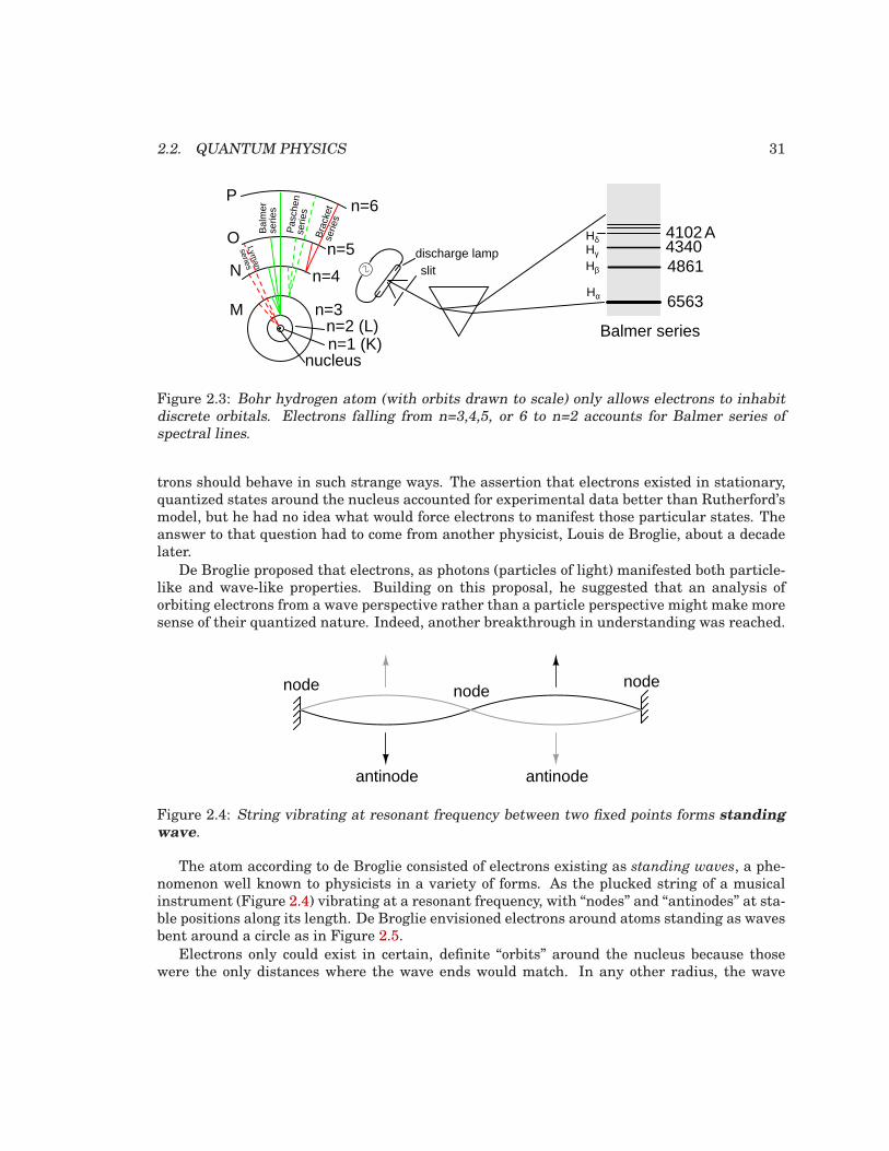
A pioneering researcher by the name of Niels Bohr attempted to improve upon Ruther-ford’s model after studying in Rutherford’s laboratory for several months in 1912. Trying toharmonize the findings of other physicists (most notably, Max Planck and Albert Einstein),Bohr suggested that each electron had a certain, specific amount of energy, and that their or-bits were quantized such that each may occupy certain places around the nucleus, as marblesfixed in circular tracks around the nucleus rather than the free-ranging satellites each wereformerly imagined to be. (Figure 2.3) In deference to the laws of electromagnetics and acceler-ating charges, Bohr alluded to these “orbits” as stationary states to escape the implication thatthey were in motion.
Although Bohr’s ambitious attempt at re-framing the structure of the atom in terms thatagreed closer to experimental results was a milestone in physics, it was not complete. Hismathematical analysis produced better predictions of experimental events than analyses be-longing to previous models, but there were still some unanswered questions about why elec-
2.2. QUANTUM PHYSICS 31
6563
43404102A
4861
Hα
Hβ
Hγ
Hδ
n=6
n=5
n=4
n=3n=2 (L)n=1 (K)
M
N
P
O
nucleus
Balmer series
Bal
mer
se
ries
Bra
cket
se
ries
Pas
chen
se
ries
Lyman
series
slitdischarge lamp
Figure 2.3: Bohr hydrogen atom (with orbits drawn to scale) only allows electrons to inhabitdiscrete orbitals. Electrons falling from n=3,4,5, or 6 to n=2 accounts for Balmer series ofspectral lines.
trons should behave in such strange ways. The assertion that electrons existed in stationary,quantized states around the nucleus accounted for experimental data better than Rutherford’smodel, but he had no idea what would force electrons to manifest those particular states. Theanswer to that question had to come from another physicist, Louis de Broglie, about a decadelater.
De Broglie proposed that electrons, as photons (particles of light) manifested both particle-like and wave-like properties. Building on this proposal, he suggested that an analysis oforbiting electrons from a wave perspective rather than a particle perspective might make moresense of their quantized nature. Indeed, another breakthrough in understanding was reached.
antinode antinode
nodenode node
Figure 2.4: String vibrating at resonant frequency between two fixed points forms standing
wave.
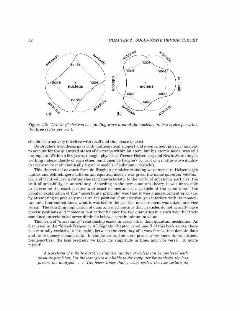
The atom according to de Broglie consisted of electrons existing as standing waves, a phe-nomenon well known to physicists in a variety of forms. As the plucked string of a musicalinstrument (Figure 2.4) vibrating at a resonant frequency, with “nodes” and “antinodes” at sta-ble positions along its length. De Broglie envisioned electrons around atoms standing as wavesbent around a circle as in Figure 2.5.
Electrons only could exist in certain, definite “orbits” around the nucleus because thosewere the only distances where the wave ends would match. In any other radius, the wave
32 CHAPTER 2. SOLID-STATE DEVICE THEORY
nucleus
antinode
antinode
node node
node
node
nucleus
nodeantinode
node
node
node
node
node
antinode
antinode
antinodeantin
ode
antinode
antinode
antinode
(a) (b)
Figure 2.5: “Orbiting” electron as standing wave around the nucleus, (a) two cycles per orbit,(b) three cycles per orbit.
should destructively interfere with itself and thus cease to exist.De Broglie’s hypothesis gave both mathematical support and a convenient physical analogy
to account for the quantized states of electrons within an atom, but his atomic model was stillincomplete. Within a few years, though, physicists Werner Heisenberg and Erwin Schrodinger,working independently of each other, built upon de Broglie’s concept of a matter-wave dualityto create more mathematically rigorous models of subatomic particles.
This theoretical advance from de Broglie’s primitive standing wave model to Heisenberg’smatrix and Schrodinger’s differential equation models was given the name quantum mechan-
ics, and it introduced a rather shocking characteristic to the world of subatomic particles: thetrait of probability, or uncertainty. According to the new quantum theory, it was impossibleto determine the exact position and exact momentum of a particle at the same time. Thepopular explanation of this “uncertainty principle” was that it was a measurement error (i.e.by attempting to precisely measure the position of an electron, you interfere with its momen-tum and thus cannot know what it was before the position measurement was taken, and viceversa). The startling implication of quantum mechanics is that particles do not actually haveprecise positions and momenta, but rather balance the two quantities in a such way that theircombined uncertainties never diminish below a certain minimum value.
This form of “uncertainty” relationship exists in areas other than quantum mechanics. Asdiscussed in the “Mixed-Frequency AC Signals” chapter in volume II of this book series, thereis a mutually exclusive relationship between the certainty of a waveform’s time-domain dataand its frequency-domain data. In simple terms, the more precisely we know its constituentfrequency(ies), the less precisely we know its amplitude in time, and vice versa. To quotemyself:
A waveform of infinite duration (infinite number of cycles) can be analyzed with
absolute precision, but the less cycles available to the computer for analysis, the less
precise the analysis. . . The fewer times that a wave cycles, the less certain its
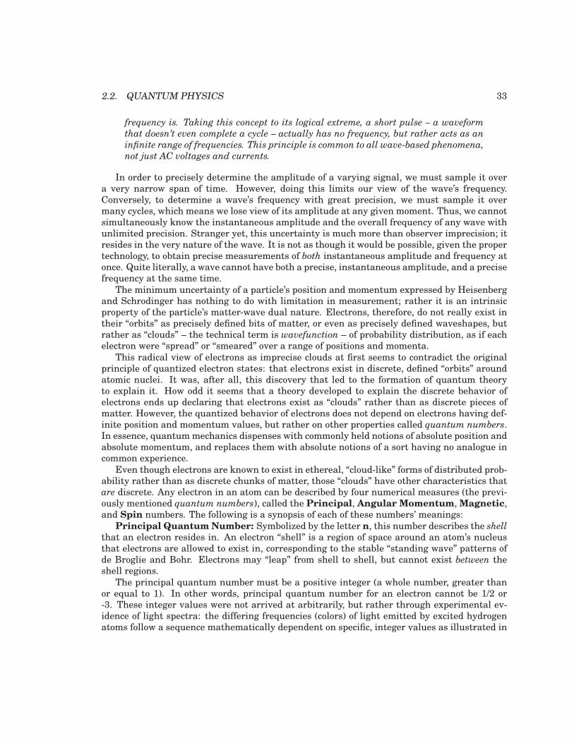
2.2. QUANTUM PHYSICS 33
frequency is. Taking this concept to its logical extreme, a short pulse – a waveform
that doesn’t even complete a cycle – actually has no frequency, but rather acts as an
infinite range of frequencies. This principle is common to all wave-based phenomena,
not just AC voltages and currents.
In order to precisely determine the amplitude of a varying signal, we must sample it overa very narrow span of time. However, doing this limits our view of the wave’s frequency.Conversely, to determine a wave’s frequency with great precision, we must sample it overmany cycles, which means we lose view of its amplitude at any given moment. Thus, we cannotsimultaneously know the instantaneous amplitude and the overall frequency of any wave withunlimited precision. Stranger yet, this uncertainty is much more than observer imprecision; itresides in the very nature of the wave. It is not as though it would be possible, given the propertechnology, to obtain precise measurements of both instantaneous amplitude and frequency atonce. Quite literally, a wave cannot have both a precise, instantaneous amplitude, and a precisefrequency at the same time.
The minimum uncertainty of a particle’s position and momentum expressed by Heisenbergand Schrodinger has nothing to do with limitation in measurement; rather it is an intrinsicproperty of the particle’s matter-wave dual nature. Electrons, therefore, do not really exist intheir “orbits” as precisely defined bits of matter, or even as precisely defined waveshapes, butrather as “clouds” – the technical term is wavefunction – of probability distribution, as if eachelectron were “spread” or “smeared” over a range of positions and momenta.
This radical view of electrons as imprecise clouds at first seems to contradict the originalprinciple of quantized electron states: that electrons exist in discrete, defined “orbits” aroundatomic nuclei. It was, after all, this discovery that led to the formation of quantum theoryto explain it. How odd it seems that a theory developed to explain the discrete behavior ofelectrons ends up declaring that electrons exist as “clouds” rather than as discrete pieces ofmatter. However, the quantized behavior of electrons does not depend on electrons having def-inite position and momentum values, but rather on other properties called quantum numbers.In essence, quantummechanics dispenses with commonly held notions of absolute position andabsolute momentum, and replaces them with absolute notions of a sort having no analogue incommon experience.
Even though electrons are known to exist in ethereal, “cloud-like” forms of distributed prob-ability rather than as discrete chunks of matter, those “clouds” have other characteristics thatare discrete. Any electron in an atom can be described by four numerical measures (the previ-ously mentioned quantum numbers), called the Principal, Angular Momentum, Magnetic,and Spin numbers. The following is a synopsis of each of these numbers’ meanings:
Principal QuantumNumber: Symbolized by the letter n, this number describes the shellthat an electron resides in. An electron “shell” is a region of space around an atom’s nucleusthat electrons are allowed to exist in, corresponding to the stable “standing wave” patterns ofde Broglie and Bohr. Electrons may “leap” from shell to shell, but cannot exist between theshell regions.
The principal quantum number must be a positive integer (a whole number, greater thanor equal to 1). In other words, principal quantum number for an electron cannot be 1/2 or-3. These integer values were not arrived at arbitrarily, but rather through experimental ev-idence of light spectra: the differing frequencies (colors) of light emitted by excited hydrogenatoms follow a sequence mathematically dependent on specific, integer values as illustrated in
34 CHAPTER 2. SOLID-STATE DEVICE THEORY
Figure 2.3.
Each shell has the capacity to hold multiple electrons. An analogy for electron shells is theconcentric rows of seats of an amphitheater. Just as a person seated in an amphitheater mustchoose a row to sit in (one cannot sit between rows), electrons must “choose” a particular shellto “sit” in. As in amphitheater rows, the outermost shells hold more electrons than the innershells. Also, electrons tend to seek the lowest available shell, as people in an amphitheaterseek the closest seat to the center stage. The higher the shell number, the greater the energyof the electrons in it.
The maximum number of electrons that any shell may hold is described by the equation 2n2,where “n” is the principal quantum number. Thus, the first shell (n=1) can hold 2 electrons;the second shell (n=2) 8 electrons, and the third shell (n=3) 18 electrons. (Figure 2.6)
n = 1 2 3 42n2 = 2 8 18 32
K L M N O P Q
observed fill = 2 8 18 32 18 18 2
Figure 2.6: Principal quantum number n and maximum number of electrons per shell bothpredicted by 2(n2), and observed. Orbitals not to scale.
Electron shells in an atom were formerly designated by letter rather than by number. Thefirst shell (n=1) was labeled K, the second shell (n=2) L, the third shell (n=3) M, the fourthshell (n=4) N, the fifth shell (n=5) O, the sixth shell (n=6) P, and the seventh shell (n=7) Q.
Angular Momentum Quantum Number: A shell, is composed of subshells. One mightbe inclined to think of subshells as simple subdivisions of shells, as lanes dividing a road.The subshells are much stranger. Subshells are regions of space where electron “clouds” areallowed to exist, and different subshells actually have different shapes. The first subshellis shaped like a sphere, (Figure 2.7(s) ) which makes sense when visualized as a cloud ofelectrons surrounding the atomic nucleus in three dimensions. The second subshell, however,resembles a dumbbell, comprised of two “lobes” joined together at a single point near the atom’scenter. (Figure 2.7(p) ) The third subshell typically resembles a set of four “lobes” clusteredaround the atom’s nucleus. These subshell shapes are reminiscent of graphical depictions ofradio antenna signal strength, with bulbous lobe-shaped regions extending from the antennain various directions. (Figure 2.7(d) )
Valid angular momentum quantum numbers are positive integers like principal quantumnumbers, but also include zero. These quantum numbers for electrons are symbolized by theletter l. The number of subshells in a shell is equal to the shell’s principal quantum num-ber. Thus, the first shell (n=1) has one subshell, numbered 0; the second shell (n=2) has twosubshells, numbered 0 and 1; the third shell (n=3) has three subshells, numbered 0, 1, and 2.
2.2. QUANTUM PHYSICS 35
x
y
z
(p) (dx2-y2)(s)
x
(dz2)
px shown py, pz similar
dx2-y2 shown dxy, dyz, dxz similar
1 of 51 of 3 1 of 5
dz2 shown
1 of 1
Figure 2.7: Orbitals: (s) Three fold symmetry. (p) Shown: px, one of three possible orientations(px, py, pz ), about their respective axes. (d) Shown: dx
2-y2 similar to dxy, dyz, dxz. Shown: dz
2.Possible d-orbital orientations: five.
An older convention for subshell description used letters rather than numbers. In this nota-tion, the first subshell (l=0) was designated s, the second subshell (l=1) designated p, the thirdsubshell (l=2) designated d, and the fourth subshell (l=3) designated f. The letters come fromthe words sharp, principal (not to be confused with the principal quantum number, n), diffuse,and fundamental. You will still see this notational convention in many periodic tables, used todesignate the electron configuration of the atoms’ outermost, or valence, shells. (Figure 2.8)
n = 1K
2 8 18 118
n = 1
2 126
26
10 26
SLPL
SK
SMPM
DM
SNPN SO
(a) (b)
l = 0 0,1 0, 1, 2 0,1, 2 02 3 4 5
electrons
2 3 4 51s2 2s22p6 3s23p63d10 4s24p64d10 5s1
10
DN
L M N O
spectroscopic notation
Figure 2.8: (a) Bohr representation of Silver atom, (b) Subshell representation of Ag withdivision of shells into subshells (angular quantum number l). This diagram implies nothingabout the actual position of electrons, but represents energy levels.
Magnetic Quantum Number: The magnetic quantum number for an electron classifieswhich orientation its subshell shape is pointed. The “lobes” for subshells point in multipledirections. These different orientations are called orbitals. For the first subshell (s; l=0), whichresembles a sphere pointing in no “direction”, so there is only one orbital. For the second(p; l=1) subshell in each shell, which resembles dumbbells point in three possible directions.
36 CHAPTER 2. SOLID-STATE DEVICE THEORY
Think of three dumbbells intersecting at the origin, each oriented along a different axis in athree-axis coordinate space.
Valid numerical values for this quantum number consist of integers ranging from -l to l, andare symbolized as ml in atomic physics and lz in nuclear physics. To calculate the number oforbitals in any given subshell, double the subshell number and add 1, (2·l + 1). For example, thefirst subshell (l=0) in any shell contains a single orbital, numbered 0; the second subshell (l=1)in any shell contains three orbitals, numbered -1, 0, and 1; the third subshell (l=2) containsfive orbitals, numbered -2, -1, 0, 1, and 2; and so on.
Like principal quantum numbers, the magnetic quantum number arose directly from ex-perimental evidence: The Zeeman effect, the division of spectral lines by exposing an ionizedgas to a magnetic field, hence the name “magnetic” quantum number.
Spin Quantum Number: Like the magnetic quantum number, this property of atomicelectrons was discovered through experimentation. Close observation of spectral lines revealedthat each line was actually a pair of very closely-spaced lines, and this so-called fine structure
was hypothesized to result from each electron “spinning” on an axis as if a planet. Electronswith different “spins” would give off slightly different frequencies of light when excited. Thename “spin” was assigned to this quantum number. The concept of a spinning electron is nowobsolete, being better suited to the (incorrect) view of electrons as discrete chunks of matterrather than as “clouds”; but, the name remains.
Spin quantum numbers are symbolized as ms in atomic physics and sz in nuclear physics.For each orbital in each subshell in each shell, there may be two electrons, one with a spin of+1/2 and the other with a spin of -1/2.
The physicist Wolfgang Pauli developed a principle explaining the ordering of electronsin an atom according to these quantum numbers. His principle, called the Pauli exclusion
principle, states that no two electrons in the same atom may occupy the exact same quantumstates. That is, each electron in an atom has a unique set of quantum numbers. This limits thenumber of electrons that may occupy any given orbital, subshell, and shell.
Shown here is the electron arrangement for a hydrogen atom:
HydrogenAtomic number (Z) = 1(one proton in nucleus)
K shell(n = 1)
subshell(l)
orbital(ml)
spin(ms)
0 0 1/2 One electron
Spectroscopic notation: 1s1
With one proton in the nucleus, it takes one electron to electrostatically balance the atom(the proton’s positive electric charge exactly balanced by the electron’s negative electric charge).This one electron resides in the lowest shell (n=1), the first subshell (l=0), in the only orbital(spatial orientation) of that subshell (ml=0), with a spin value of 1/2. A common method ofdescribing this organization is by listing the electrons according to their shells and subshells
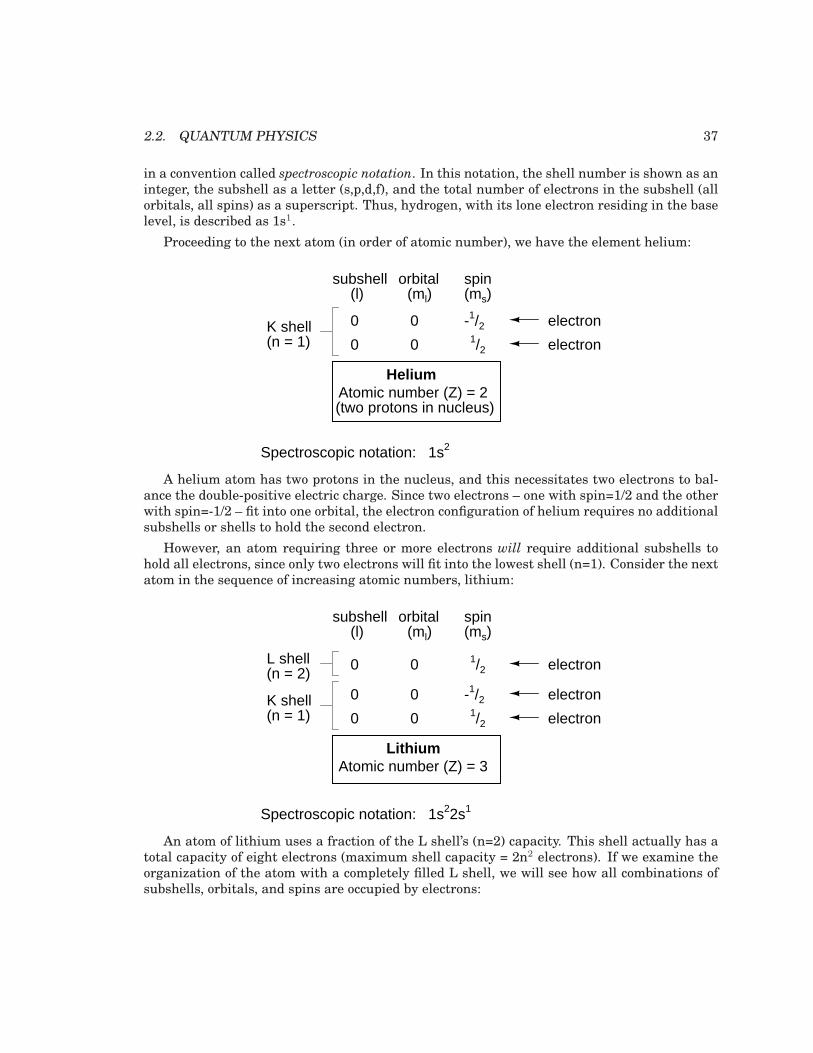
2.2. QUANTUM PHYSICS 37
in a convention called spectroscopic notation. In this notation, the shell number is shown as aninteger, the subshell as a letter (s,p,d,f), and the total number of electrons in the subshell (allorbitals, all spins) as a superscript. Thus, hydrogen, with its lone electron residing in the baselevel, is described as 1s1.
Proceeding to the next atom (in order of atomic number), we have the element helium:
K shell(n = 1)
subshell(l)
orbital(ml)
spin(ms)
0 0 1/2
Spectroscopic notation:
HeliumAtomic number (Z) = 2(two protons in nucleus)
0 0 -1/2 electron
electron
1s2
A helium atom has two protons in the nucleus, and this necessitates two electrons to bal-ance the double-positive electric charge. Since two electrons – one with spin=1/2 and the otherwith spin=-1/2 – fit into one orbital, the electron configuration of helium requires no additionalsubshells or shells to hold the second electron.
However, an atom requiring three or more electrons will require additional subshells tohold all electrons, since only two electrons will fit into the lowest shell (n=1). Consider the nextatom in the sequence of increasing atomic numbers, lithium:
K shell(n = 1)
subshell(l)
orbital(ml)
spin(ms)
0 0 1/2
Spectroscopic notation:
0 0 -1/2 electron
electron
LithiumAtomic number (Z) = 3
L shell(n = 2)
0 0 1/2 electron
1s22s1
An atom of lithium uses a fraction of the L shell’s (n=2) capacity. This shell actually has atotal capacity of eight electrons (maximum shell capacity = 2n2 electrons). If we examine theorganization of the atom with a completely filled L shell, we will see how all combinations ofsubshells, orbitals, and spins are occupied by electrons:
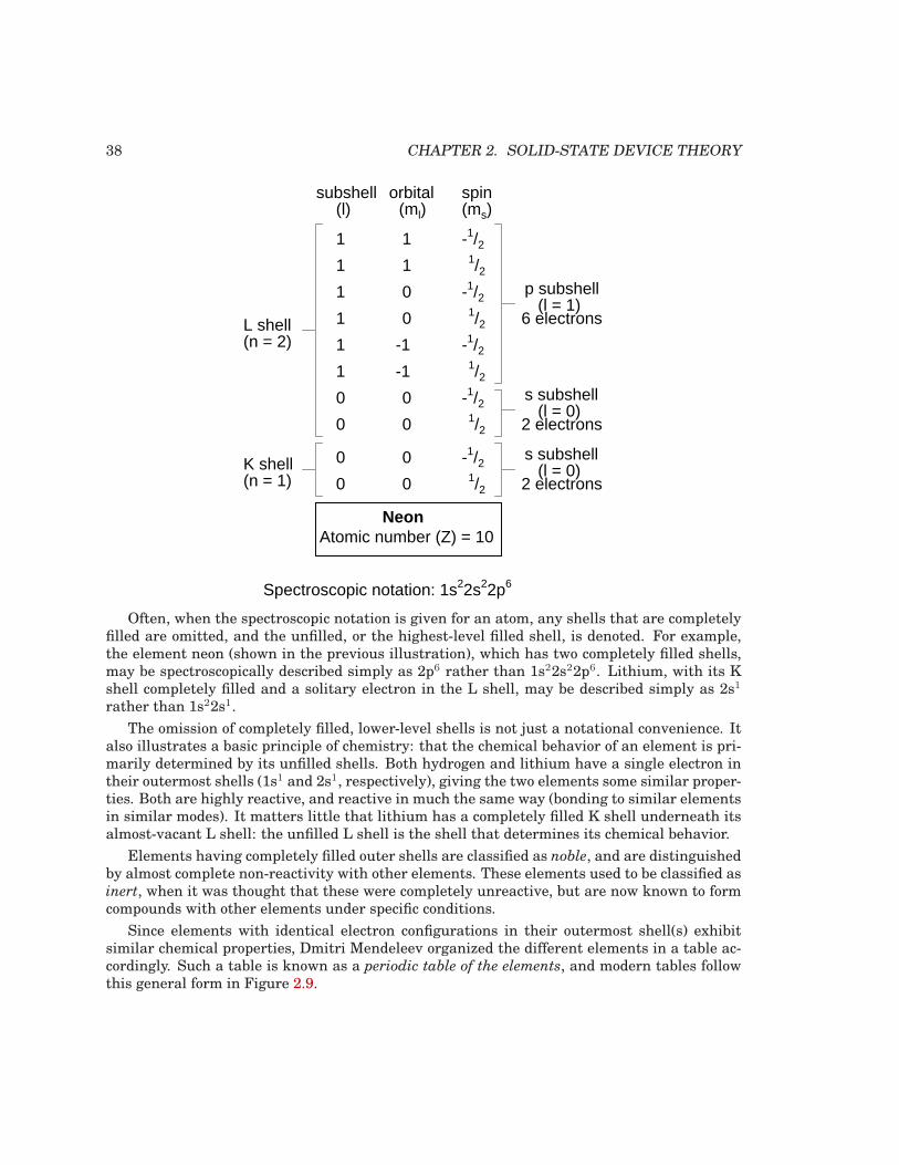
38 CHAPTER 2. SOLID-STATE DEVICE THEORY
K shell(n = 1)
subshell(l)
orbital(ml)
spin(ms)
0 0 1/2
0 0 -1/2
L shell(n = 2)
0 0 1/2
NeonAtomic number (Z) = 10
0 0 -1/2
1
1
1
1
1
1
-1 1/2
-1 -1/2
0
0
-1/21/2
1
1 -1/21/2
s subshell(l = 0)
s subshell(l = 0)
p subshell(l = 1)
2 electrons
2 electrons
6 electrons
Spectroscopic notation: 1s22s22p6
Often, when the spectroscopic notation is given for an atom, any shells that are completelyfilled are omitted, and the unfilled, or the highest-level filled shell, is denoted. For example,the element neon (shown in the previous illustration), which has two completely filled shells,may be spectroscopically described simply as 2p6 rather than 1s22s22p6. Lithium, with its Kshell completely filled and a solitary electron in the L shell, may be described simply as 2s1
rather than 1s22s1.
The omission of completely filled, lower-level shells is not just a notational convenience. Italso illustrates a basic principle of chemistry: that the chemical behavior of an element is pri-marily determined by its unfilled shells. Both hydrogen and lithium have a single electron intheir outermost shells (1s1 and 2s1, respectively), giving the two elements some similar proper-ties. Both are highly reactive, and reactive in much the same way (bonding to similar elementsin similar modes). It matters little that lithium has a completely filled K shell underneath itsalmost-vacant L shell: the unfilled L shell is the shell that determines its chemical behavior.
Elements having completely filled outer shells are classified as noble, and are distinguishedby almost complete non-reactivity with other elements. These elements used to be classified asinert, when it was thought that these were completely unreactive, but are now known to formcompounds with other elements under specific conditions.
Since elements with identical electron configurations in their outermost shell(s) exhibitsimilar chemical properties, Dmitri Mendeleev organized the different elements in a table ac-cordingly. Such a table is known as a periodic table of the elements, and modern tables followthis general form in Figure 2.9.
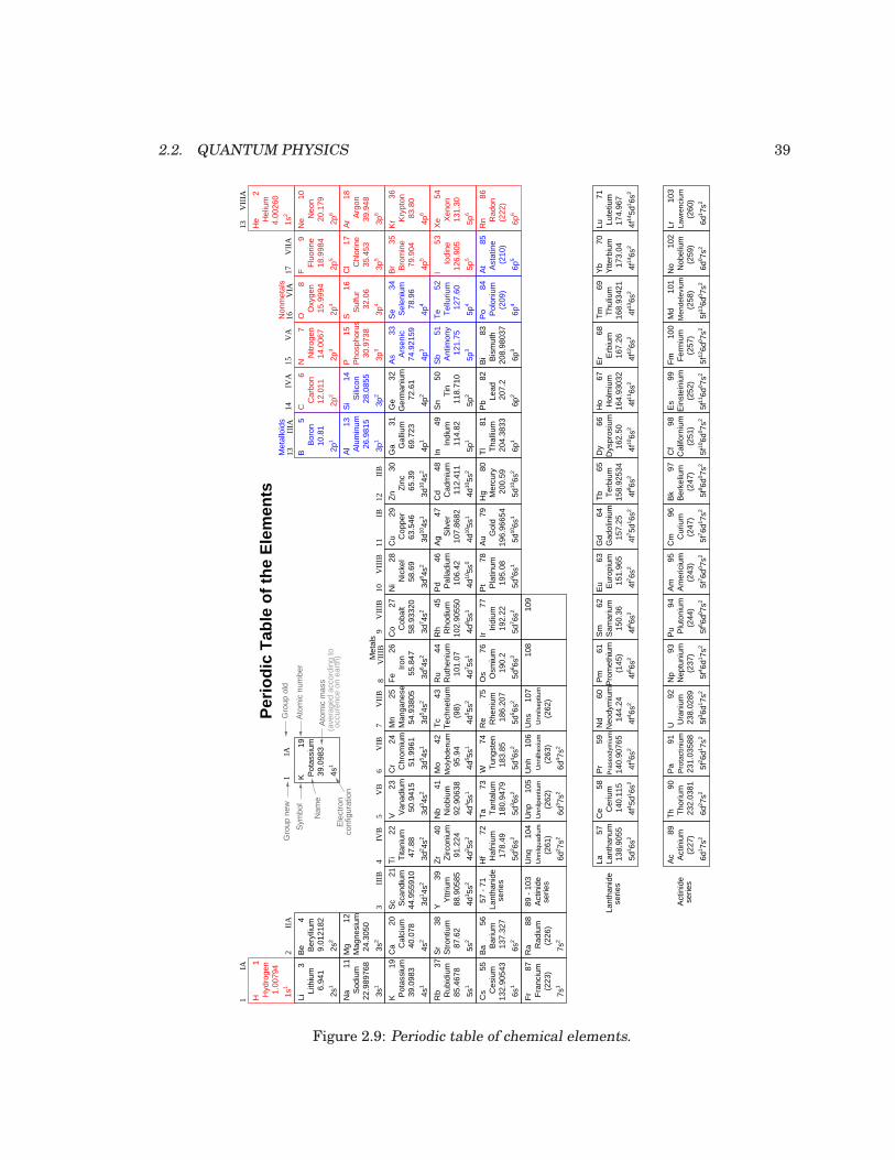
2.2. QUANTUM PHYSICS 39
Pot
assi
umK
19
39.0
983
4s1
Cal
cium
Ca
20
4s2
Na S
odiu
m11
3s1
Mag
nesi
umM
g12
3s2
H1
Hyd
roge
n
1s1
LiLi
thiu
m6.
941
3
2s1
Ber
ylliu
mB
e4
2s2
Sc
21S
cand
ium
3d1 4s
2
Ti
22T
itani
um
3d2 4s
2
V23
Van
adiu
m50
.941
5
3d3 4s
2
Cr
24C
hrom
ium
3d5 4s
1
Mn
25M
anga
nese
3d5 4s
2
Fe
26Ir
on55
.847
3d6 4s
2
Co
27C
obal
t
3d7 4s
2
Ni
28N
icke
l
3d8 4s
2
Cu
29C
oppe
r63
.546
3d10
4s1
Zn
30Z
inc
3d10
4s2
Ga
31G
alliu
m
4p1
B5
Bor
on10
.81
2p1
C6
Car
bon
12.0
11
2p2
N7
Nitr
ogen
14.0
067
2p3
O8
Oxy
gen
15.9
994
2p4
F9
Flu
orin
e18
.998
4
2p5
He
2H
eliu
m4.
0026
0
1s2
Ne
10N
eon
20.1
79
2p6
Ar
18A
rgon
39.9
48
3p6
Kr
36K
rypt
on83
.80
4p6
Xe
54X
enon
131.
30
5p6
Rn
86R
adon
(222
)
6p6
K Pot
assi
um19
39.0
983
4s1
Sym
bol
Ato
mic
num
ber
Nam
eA
tom
ic m
ass
Ele
ctro
nco
nfig
urat
ion
Al
13A
lum
inum
26.9
815
3p1
Si
14S
ilico
n28
.085
5
3p2
P15
Pho
spho
rus
30.9
738
3p3
S16
Sul
fur
32.0
6
3p4
Cl
17C
hlor
ine
35.4
53
3p5
Per
iod
ic T
able
of
the
Ele
men
ts
Ger
man
ium
4p2
Ge
32A
s Ars
enic33
4p3
Se Sel
eniu
m34
78.9
6
4p4
Br Bro
min
e35
79.9
04
4p5
IIo
dine
53
126.
905
5p5
Rub
idiu
m37
85.4
678
5s1
Sr
Str
ontiu
m38
87.6
2
5s2
Yttr
ium
Y39
4d1 5s
2
Zr
40Z
ircon
ium
91.2
24
4d2 5s
2
Nb
41N
iobi
um92
.906
38
4d4 5s
1
Mo
42M
olyb
denu
m95
.94
4d5 5s
1
Tc
43T
echn
etiu
m(9
8)
4d5 5s
2
Ru
44R
uthe
nium
101.
07
4d7 5s
1
Rh
45R
hodi
um
4d8 5s
1
Pd
46P
alla
dium
106.
42
4d10
5s0
Ag
47S
ilver
107.
8682
4d10
5s1
Cd
48C
adm
ium
112.
411
4d10
5s2
In49
Indi
um11
4.82
5p1
Sn
50T
in11
8.71
0
5p2
Sb
51A
ntim
ony
121.
75
5p3
Te
52T
ellu
rium
127.
60
5p4
Po
84P
olon
ium
(209
)
6p4
At Ast
atin
e85
(210
)
6p5
Met
als
Met
allo
ids
Non
met
als
Rb
Cs
55C
esiu
m13
2.90
543
6s1
Ba
56B
ariu
m13
7.32
7
6s2
57 -
71
Lant
hani
dese
ries
Hf
72H
afni
um17
8.49
5d2 6s
2
Ta Tan
talu
m73
180.
9479
5d3 6s
2
W74
Tun
gste
n18
3.85
5d4 6s
2
Re
75R
heni
um18
6.20
7
5d5 6s
2
Os
76O
smiu
m19
0.2
5d6 6s
2
Ir77
192.
22Ir
idiu
m
5d7 6s
2
Pt
78P
latin
um19
5.08
5d9 6s
1
Au G
old
79
196.
9665
4
5d10
6s1
Hg
80M
ercu
ry20
0.59
5d10
6s2
Tl
81T
halli
um20
4.38
33
6p1
Pb Le
ad82
207.
2
6p2
Bi Bis
mut
h83
208.
9803
7
6p3
Lant
hani
dese
ries
Fr
87F
ranc
ium
(223
)
7s1
Ra
88R
adiu
m(2
26)
7s2
89 -
103
Act
inid
ese
ries
Act
inid
ese
ries
104
Unq
Unn
ilqua
dium
(261
)
6d2 7s
2
Unp
105
Unn
ilpen
tium
(262
)
6d3 7s
2
Unh
106
Unn
ilhex
ium
(263
)
6d4 7s
2
Uns
107
Unn
ilsep
tium
(262
)
108
109
1.00
794
9.01
2182
22.9
8976
824
.305
0
40.0
7844
.955
910
47.8
851
.996
154
.938
0558
.933
2058
.69
65.3
969
.723
72.6
174
.921
59
88.9
0585
102.
9055
0
(ave
rage
d ac
cord
ing
tooc
cure
nce
on e
arth
)
La57
Lant
hanu
m13
8.90
55
5d1 6s
2
Ce
58C
eriu
m14
0.11
5
4f1 5d
1 6s2
Pr
59P
rase
odym
ium
140.
9076
5
4f3 6s
2
Nd
60N
eody
miu
m14
4.24
4f4 6s
2
Pm
61P
rom
ethi
um(1
45)
4f5 6s
2
Sm
62S
amar
ium
150.
36
4f6 6s
2
Eu
63E
urop
ium
151.
965
4f7 6s
2
Gd
64G
adol
iniu
m15
7.25
4f7 5d
1 6s2
Tb
65
158.
9253
4T
erbi
um
4f9 6s
2
Dy
66D
yspr
osiu
m16
2.50
4f10
6s2
Ho
67H
olm
ium
164.
9303
2
4f11
6s2
Er
68E
rbiu
m16
7.26
4f12
6s2
Tm
69T
huliu
m16
8.93
421
4f13
6s2
Yb
70Y
tterb
ium
173.
04
4f14
6s2
Lu71
Lute
tium
174.
967
4f14
5d1 6s
2
Ac Act
iniu
m89
(227
)
6d1 7s
2
Th
90T
horiu
m23
2.03
81
6d2 7s
2
Pa
91P
rota
ctin
ium
231.
0358
8
5f2 6d
1 7s2
U92
Ura
nium
238.
0289
5f3 6d
1 7s2
Np
93N
eptu
nium
(237
)
5f4 6d
1 7s2
Pu
94P
luto
nium
(244
)
5f6 6d
0 7s2
Am
95A
mer
iciu
m(2
43)
5f7 6d
0 7s2
Cm
96C
uriu
m(2
47)
5f7 6d
1 7s2
Bk
97B
erke
lium
(247
)
5f9 6d
0 7s2
Cf
98C
alifo
rniu
m(2
51)
5f10
6d0 7s
2
Es
99E
inst
eini
um(2
52)
5f11
6d0 7s
2
Fm
100
Fer
miu
m(2
57)
5f12
6d0 7s
2
Md
101
Men
dele
vium
(258
)
5f13
6d0 7s
2
No
102
Nob
eliu
m(2
59)
6d0 7s
2
Lr10
3La
wre
nciu
m(2
60)
6d1 7s
2
1
IAG
roup
new
Gro
up o
ld
3
IIIB
2
IIA
1
I
A
4
I
VB
5
V
B6
VIB
7
V
IIB
8
V
IIIB
9
VII
IB10
V
IIIB
12
I
IB
13
I
IIA
14
I
VA
15
V
A16
VIA
17
V
IIA
13
VII
IA
11
IB
Figure 2.9: Periodic table of chemical elements.
40 CHAPTER 2. SOLID-STATE DEVICE THEORY
Dmitri Mendeleev, a Russian chemist, was the first to develop a periodic table of the ele-ments. Although Mendeleev organized his table according to atomic mass rather than atomicnumber, and produced a table that was not quite as useful as modern periodic tables, his de-velopment stands as an excellent example of scientific proof. Seeing the patterns of periodicity(similar chemical properties according to atomic mass), Mendeleev hypothesized that all el-ements should fit into this ordered scheme. When he discovered “empty” spots in the table,he followed the logic of the existing order and hypothesized the existence of heretofore undis-covered elements. The subsequent discovery of those elements granted scientific legitimacy toMendeleev’s hypothesis, furthering future discoveries, and leading to the form of the periodictable we use today.
This is how science should work: hypotheses followed to their logical conclusions, and ac-cepted, modified, or rejected as determined by the agreement of experimental data to thoseconclusions. Any fool may formulate a hypothesis after-the-fact to explain existing experimen-tal data, and many do. What sets a scientific hypothesis apart from post hoc speculation isthe prediction of future experimental data yet uncollected, and the possibility of disproof as aresult of that data. To boldly follow a hypothesis to its logical conclusion(s) and dare to predictthe results of future experiments is not a dogmatic leap of faith, but rather a public test of thathypothesis, open to challenge from anyone able to produce contradictory data. In other words,scientific hypotheses are always “risky” due to the claim to predict the results of experimentsnot yet conducted, and are therefore susceptible to disproof if the experiments do not turn outas predicted. Thus, if a hypothesis successfully predicts the results of repeated experiments,its falsehood is disproven.
Quantum mechanics, first as a hypothesis and later as a theory, has proven to be extremelysuccessful in predicting experimental results, hence the high degree of scientific confidenceplaced in it. Many scientists have reason to believe that it is an incomplete theory, though,as its predictions hold true more at micro physical scales than at macroscopic dimensions, butnevertheless it is a tremendously useful theory in explaining and predicting the interactionsof particles and atoms.
As you have already seen in this chapter, quantum physics is essential in describing andpredicting many different phenomena. In the next section, we will see its significance in theelectrical conductivity of solid substances, including semiconductors. Simply put, nothing inchemistry or solid-state physics makes sense within the popular theoretical framework of elec-trons existing as discrete chunks of matter, whirling around atomic nuclei like miniature satel-lites. It is when electrons are viewed as “wavefunctions” existing in definite, discrete statesthat the regular and periodic behavior of matter can be explained.
• REVIEW:
• Electrons in atoms exist in “clouds” of distributed probability, not as discrete chunks ofmatter orbiting the nucleus like tiny satellites, as common illustrations of atoms show.
• Individual electrons around an atomic nucleus seek unique “states,” described by fourquantum numbers: the Principal Quantum Number, known as the shell; the Angular
Momentum Quantum Number, known as the subshell; the Magnetic Quantum Number,describing the orbital (subshell orientation); and the Spin Quantum Number, or simplyspin. These states are quantized, meaning that no “in-between” conditions exist for anelectron other than those states that fit into the quantum numbering scheme.
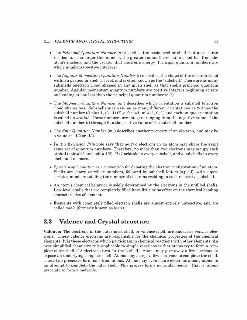
2.3. VALENCE AND CRYSTAL STRUCTURE 41
• The Principal Quantum Number (n) describes the basic level or shell that an electronresides in. The larger this number, the greater radius the electron cloud has from theatom’s nucleus, and the greater that electron’s energy. Principal quantum numbers arewhole numbers (positive integers).
• The Angular Momentum Quantum Number (l) describes the shape of the electron cloudwithin a particular shell or level, and is often known as the “subshell.” There are as manysubshells (electron cloud shapes) in any given shell as that shell’s principal quantumnumber. Angular momentum quantum numbers are positive integers beginning at zeroand ending at one less than the principal quantum number (n-1).
• The Magnetic Quantum Number (ml) describes which orientation a subshell (electroncloud shape) has. Subshells may assume as many different orientations as 2-times thesubshell number (l) plus 1, (2l+1) (E.g. for l=1, ml= -1, 0, 1) and each unique orientationis called an orbital. These numbers are integers ranging from the negative value of thesubshell number (l) through 0 to the positive value of the subshell number.
• The Spin Quantum Number (ms) describes another property of an electron, and may bea value of +1/2 or -1/2.
• Pauli’s Exclusion Principle says that no two electrons in an atom may share the exactsame set of quantum numbers. Therefore, no more than two electrons may occupy eachorbital (spin=1/2 and spin=-1/2), 2l+1 orbitals in every subshell, and n subshells in everyshell, and no more.
• Spectroscopic notation is a convention for denoting the electron configuration of an atom.Shells are shown as whole numbers, followed by subshell letters (s,p,d,f), with super-scripted numbers totaling the number of electrons residing in each respective subshell.
• An atom’s chemical behavior is solely determined by the electrons in the unfilled shells.Low-level shells that are completely filled have little or no effect on the chemical bondingcharacteristics of elements.
• Elements with completely filled electron shells are almost entirely unreactive, and arecalled noble (formerly known as inert).
2.3 Valence and Crystal structure
Valence: The electrons in the outer most shell, or valence shell, are known as valence elec-trons. These valence electrons are responsible for the chemical properties of the chemicalelements. It is these electrons which participate in chemical reactions with other elements. Anover simplified chemistry rule applicable to simple reactions is that atoms try to form a com-plete outer shell of 8 electrons (two for the L shell). Atoms may give away a few electrons toexpose an underlying complete shell. Atoms may accept a few electrons to complete the shell.These two processes form ions from atoms. Atoms may even share electrons among atoms inan attempt to complete the outer shell. This process forms molecular bonds. That is, atomsassociate to form a molecule.
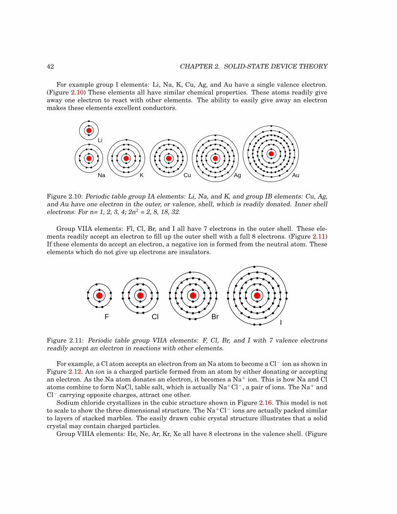
42 CHAPTER 2. SOLID-STATE DEVICE THEORY
For example group I elements: Li, Na, K, Cu, Ag, and Au have a single valence electron.(Figure 2.10) These elements all have similar chemical properties. These atoms readily giveaway one electron to react with other elements. The ability to easily give away an electronmakes these elements excellent conductors.
KNa
Li
AgCu Au
Figure 2.10: Periodic table group IA elements: Li, Na, and K, and group IB elements: Cu, Ag,and Au have one electron in the outer, or valence, shell, which is readily donated. Inner shellelectrons: For n= 1, 2, 3, 4; 2n2 = 2, 8, 18, 32.
Group VIIA elements: Fl, Cl, Br, and I all have 7 electrons in the outer shell. These ele-ments readily accept an electron to fill up the outer shell with a full 8 electrons. (Figure 2.11)If these elements do accept an electron, a negative ion is formed from the neutral atom. Theseelements which do not give up electrons are insulators.
ClF BrI
Figure 2.11: Periodic table group VIIA elements: F, Cl, Br, and I with 7 valence electronsreadily accept an electron in reactions with other elements.
For example, a Cl atom accepts an electron from an Na atom to become a Cl− ion as shown inFigure 2.12. An ion is a charged particle formed from an atom by either donating or acceptingan electron. As the Na atom donates an electron, it becomes a Na+ ion. This is how Na and Clatoms combine to form NaCl, table salt, which is actually Na+Cl−, a pair of ions. The Na+ andCl− carrying opposite charges, attract one other.
Sodium chloride crystallizes in the cubic structure shown in Figure 2.16. This model is notto scale to show the three dimensional structure. The Na+Cl− ions are actually packed similarto layers of stacked marbles. The easily drawn cubic crystal structure illustrates that a solidcrystal may contain charged particles.
Group VIIIA elements: He, Ne, Ar, Kr, Xe all have 8 electrons in the valence shell. (Figure
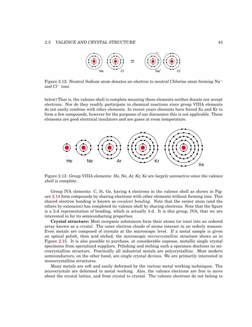
2.3. VALENCE AND CRYSTAL STRUCTURE 43
Na Cl Na+ Cl-
=+ -
Figure 2.12: Neutral Sodium atom donates an electron to neutral Chlorine atom forming Na+
and Cl− ions.
below) That is, the valence shell is complete meaning these elements neither donate nor acceptelectrons. Nor do they readily participate in chemical reactions since group VIIIA elementsdo not easily combine with other elements. In recent years chemists have forced Xe and Kr toform a few compounds, however for the purposes of our discussion this is not applicable. Theseelements are good electrical insulators and are gases at room temperature.
ArNeHe KrXe
Figure 2.13: Group VIIIA elements: He, Ne, Ar, Kr, Xe are largely unreactive since the valenceshell is complete..
Group IVA elements: C, Si, Ge, having 4 electrons in the valence shell as shown in Fig-ure 2.14 form compounds by sharing electrons with other elements without forming ions. Thisshared electron bonding is known as covalent bonding. Note that the center atom (and theothers by extension) has completed its valence shell by sharing electrons. Note that the figureis a 2-d representation of bonding, which is actually 3-d. It is this group, IVA, that we areinterested in for its semiconducting properties.
Crystal structure: Most inorganic substances form their atoms (or ions) into an orderedarray known as a crystal. The outer electron clouds of atoms interact in an orderly manner.Even metals are composed of crystals at the microscopic level. If a metal sample is givenan optical polish, then acid etched, the microscopic microcrystalline structure shows as inFigure 2.15. It is also possible to purchase, at considerable expense, metallic single crystalspecimens from specialized suppliers. Polishing and etching such a specimen discloses no mi-crocrystalline structure. Practically all industrial metals are polycrystalline. Most modernsemiconductors, on the other hand, are single crystal devices. We are primarily interested inmonocrystalline structures.
Many metals are soft and easily deformed by the various metal working techniques. Themicrocrystals are deformed in metal working. Also, the valence electrons are free to moveabout the crystal lattice, and from crystal to crystal. The valence electrons do not belong to
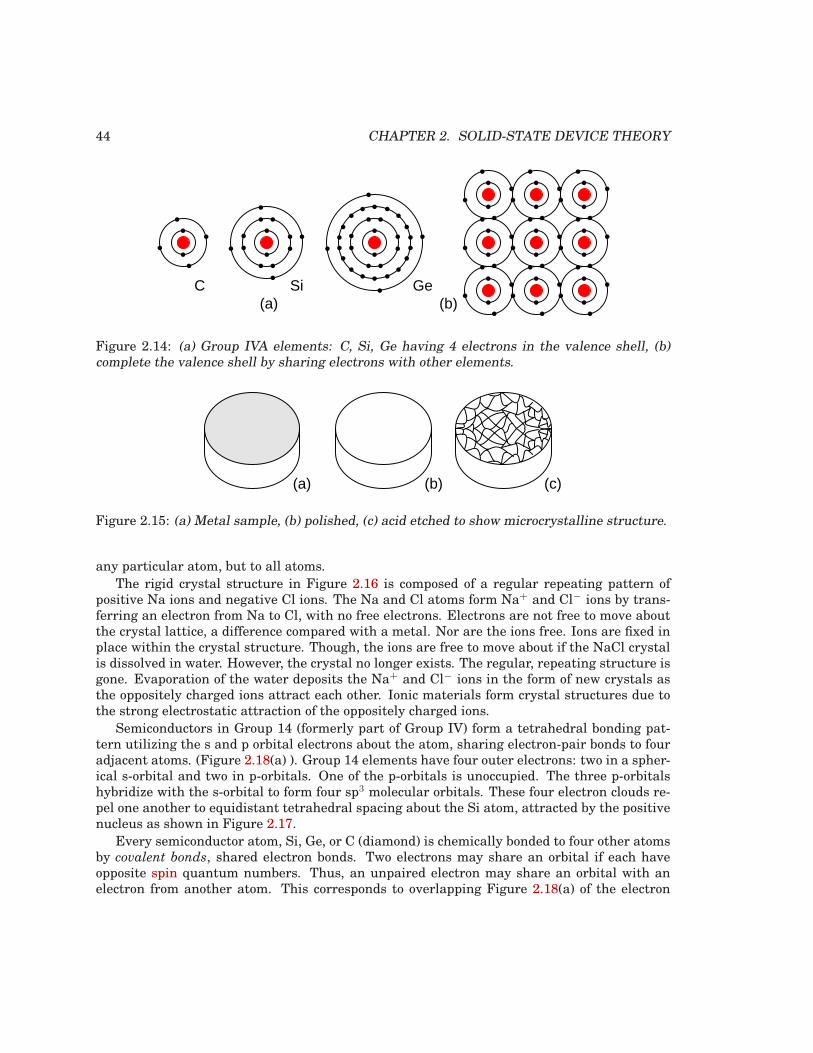
44 CHAPTER 2. SOLID-STATE DEVICE THEORY
SiC Ge(b)(a)
Figure 2.14: (a) Group IVA elements: C, Si, Ge having 4 electrons in the valence shell, (b)complete the valence shell by sharing electrons with other elements.
(a) (b) (c)
Figure 2.15: (a) Metal sample, (b) polished, (c) acid etched to show microcrystalline structure.
any particular atom, but to all atoms.
The rigid crystal structure in Figure 2.16 is composed of a regular repeating pattern ofpositive Na ions and negative Cl ions. The Na and Cl atoms form Na+ and Cl− ions by trans-ferring an electron from Na to Cl, with no free electrons. Electrons are not free to move aboutthe crystal lattice, a difference compared with a metal. Nor are the ions free. Ions are fixed inplace within the crystal structure. Though, the ions are free to move about if the NaCl crystalis dissolved in water. However, the crystal no longer exists. The regular, repeating structure isgone. Evaporation of the water deposits the Na+ and Cl− ions in the form of new crystals asthe oppositely charged ions attract each other. Ionic materials form crystal structures due tothe strong electrostatic attraction of the oppositely charged ions.
Semiconductors in Group 14 (formerly part of Group IV) form a tetrahedral bonding pat-tern utilizing the s and p orbital electrons about the atom, sharing electron-pair bonds to fouradjacent atoms. (Figure 2.18(a) ). Group 14 elements have four outer electrons: two in a spher-ical s-orbital and two in p-orbitals. One of the p-orbitals is unoccupied. The three p-orbitalshybridize with the s-orbital to form four sp3 molecular orbitals. These four electron clouds re-pel one another to equidistant tetrahedral spacing about the Si atom, attracted by the positivenucleus as shown in Figure 2.17.
Every semiconductor atom, Si, Ge, or C (diamond) is chemically bonded to four other atomsby covalent bonds, shared electron bonds. Two electrons may share an orbital if each haveopposite spin quantum numbers. Thus, an unpaired electron may share an orbital with anelectron from another atom. This corresponds to overlapping Figure 2.18(a) of the electron
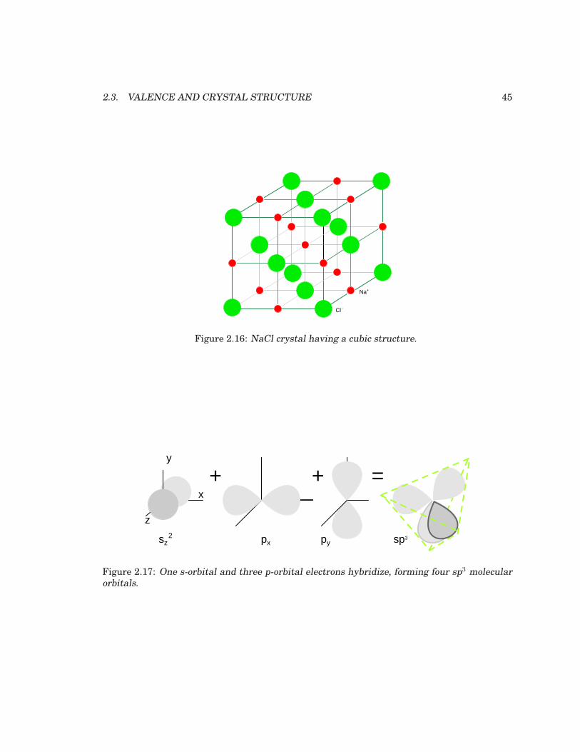
2.3. VALENCE AND CRYSTAL STRUCTURE 45
Na+
Cl -
Figure 2.16: NaCl crystal having a cubic structure.
x
y
z
px pysz2
=+ +
sp3
Figure 2.17: One s-orbital and three p-orbital electrons hybridize, forming four sp3 molecularorbitals.
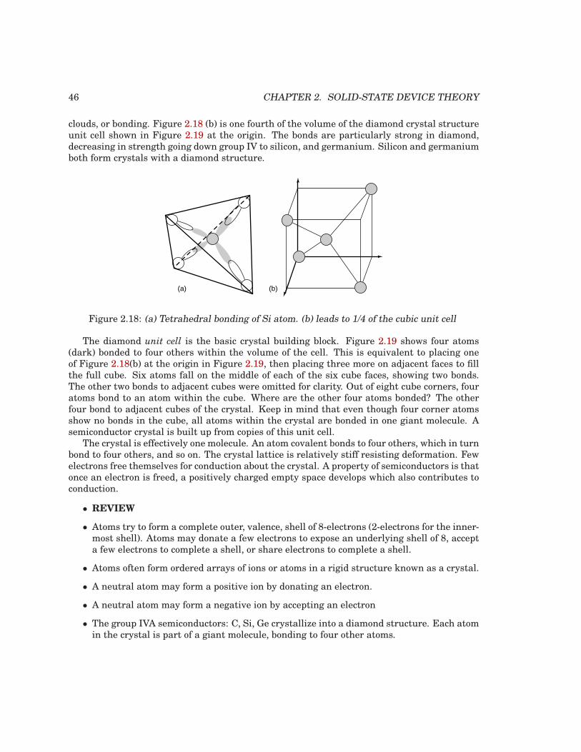
46 CHAPTER 2. SOLID-STATE DEVICE THEORY
clouds, or bonding. Figure 2.18 (b) is one fourth of the volume of the diamond crystal structureunit cell shown in Figure 2.19 at the origin. The bonds are particularly strong in diamond,decreasing in strength going down group IV to silicon, and germanium. Silicon and germaniumboth form crystals with a diamond structure.
(b)(a)
Figure 2.18: (a) Tetrahedral bonding of Si atom. (b) leads to 1/4 of the cubic unit cell
The diamond unit cell is the basic crystal building block. Figure 2.19 shows four atoms(dark) bonded to four others within the volume of the cell. This is equivalent to placing oneof Figure 2.18(b) at the origin in Figure 2.19, then placing three more on adjacent faces to fillthe full cube. Six atoms fall on the middle of each of the six cube faces, showing two bonds.The other two bonds to adjacent cubes were omitted for clarity. Out of eight cube corners, fouratoms bond to an atom within the cube. Where are the other four atoms bonded? The otherfour bond to adjacent cubes of the crystal. Keep in mind that even though four corner atomsshow no bonds in the cube, all atoms within the crystal are bonded in one giant molecule. Asemiconductor crystal is built up from copies of this unit cell.
The crystal is effectively one molecule. An atom covalent bonds to four others, which in turnbond to four others, and so on. The crystal lattice is relatively stiff resisting deformation. Fewelectrons free themselves for conduction about the crystal. A property of semiconductors is thatonce an electron is freed, a positively charged empty space develops which also contributes toconduction.
• REVIEW
• Atoms try to form a complete outer, valence, shell of 8-electrons (2-electrons for the inner-most shell). Atoms may donate a few electrons to expose an underlying shell of 8, accepta few electrons to complete a shell, or share electrons to complete a shell.
• Atoms often form ordered arrays of ions or atoms in a rigid structure known as a crystal.
• A neutral atom may form a positive ion by donating an electron.
• A neutral atom may form a negative ion by accepting an electron
• The group IVA semiconductors: C, Si, Ge crystallize into a diamond structure. Each atomin the crystal is part of a giant molecule, bonding to four other atoms.
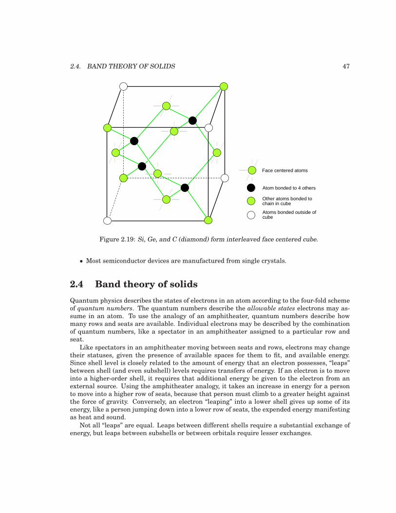
2.4. BAND THEORY OF SOLIDS 47
Atom bonded to 4 others
Atoms bonded outside ofcube
Other atoms bonded to chain in cube
Face centered atoms
Figure 2.19: Si, Ge, and C (diamond) form interleaved face centered cube.
• Most semiconductor devices are manufactured from single crystals.
2.4 Band theory of solids
Quantum physics describes the states of electrons in an atom according to the four-fold schemeof quantum numbers. The quantum numbers describe the allowable states electrons may as-sume in an atom. To use the analogy of an amphitheater, quantum numbers describe howmany rows and seats are available. Individual electrons may be described by the combinationof quantum numbers, like a spectator in an amphitheater assigned to a particular row andseat.
Like spectators in an amphitheater moving between seats and rows, electrons may changetheir statuses, given the presence of available spaces for them to fit, and available energy.Since shell level is closely related to the amount of energy that an electron possesses, “leaps”between shell (and even subshell) levels requires transfers of energy. If an electron is to moveinto a higher-order shell, it requires that additional energy be given to the electron from anexternal source. Using the amphitheater analogy, it takes an increase in energy for a personto move into a higher row of seats, because that person must climb to a greater height againstthe force of gravity. Conversely, an electron “leaping” into a lower shell gives up some of itsenergy, like a person jumping down into a lower row of seats, the expended energy manifestingas heat and sound.
Not all “leaps” are equal. Leaps between different shells require a substantial exchange ofenergy, but leaps between subshells or between orbitals require lesser exchanges.
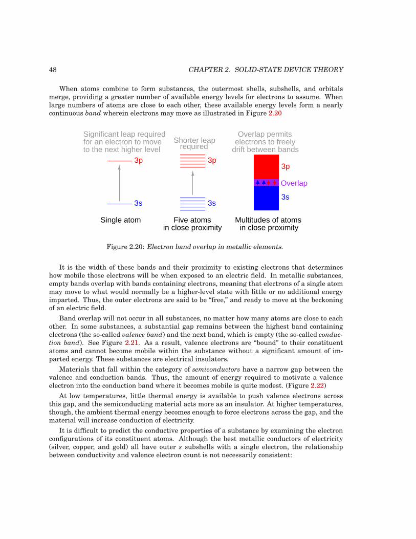
48 CHAPTER 2. SOLID-STATE DEVICE THEORY
When atoms combine to form substances, the outermost shells, subshells, and orbitalsmerge, providing a greater number of available energy levels for electrons to assume. Whenlarge numbers of atoms are close to each other, these available energy levels form a nearlycontinuous band wherein electrons may move as illustrated in Figure 2.20
3s
3p
Single atom
for an electron to moveto the next higher level
Five atomsin close proximity
Significant leap required
3p
3s
Shorter leap
3p
3s
Overlap
Multitudes of atomsin close proximity
required
Overlap permitselectrons to freely
drift between bands
Figure 2.20: Electron band overlap in metallic elements.
It is the width of these bands and their proximity to existing electrons that determineshow mobile those electrons will be when exposed to an electric field. In metallic substances,empty bands overlap with bands containing electrons, meaning that electrons of a single atommay move to what would normally be a higher-level state with little or no additional energyimparted. Thus, the outer electrons are said to be “free,” and ready to move at the beckoningof an electric field.
Band overlap will not occur in all substances, no matter how many atoms are close to eachother. In some substances, a substantial gap remains between the highest band containingelectrons (the so-called valence band) and the next band, which is empty (the so-called conduc-
tion band). See Figure 2.21. As a result, valence electrons are “bound” to their constituentatoms and cannot become mobile within the substance without a significant amount of im-parted energy. These substances are electrical insulators.
Materials that fall within the category of semiconductors have a narrow gap between thevalence and conduction bands. Thus, the amount of energy required to motivate a valenceelectron into the conduction band where it becomes mobile is quite modest. (Figure 2.22)
At low temperatures, little thermal energy is available to push valence electrons acrossthis gap, and the semiconducting material acts more as an insulator. At higher temperatures,though, the ambient thermal energy becomes enough to force electrons across the gap, and thematerial will increase conduction of electricity.
It is difficult to predict the conductive properties of a substance by examining the electronconfigurations of its constituent atoms. Although the best metallic conductors of electricity(silver, copper, and gold) all have outer s subshells with a single electron, the relationshipbetween conductivity and valence electron count is not necessarily consistent:
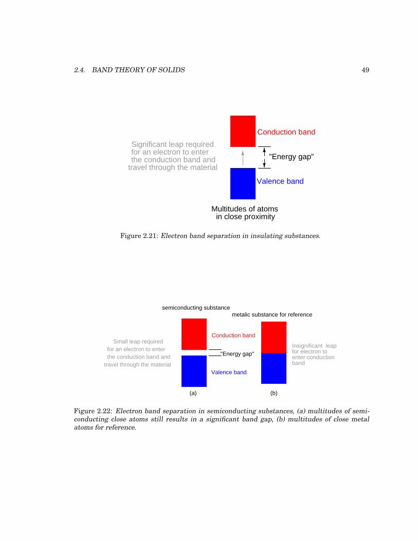
2.4. BAND THEORY OF SOLIDS 49
Multitudes of atomsin close proximity
Conduction band
Valence band
Significant leap requiredfor an electron to enterthe conduction band and
travel through the material"Energy gap"
Figure 2.21: Electron band separation in insulating substances.
(a)
Conduction band
Valence band
for an electron to enterthe conduction band and
travel through the material
"Energy gap"
semiconducting substance
Small leap required
(b)
metalic substance for reference
Insignificant leap for electron to enter conductionband
Figure 2.22: Electron band separation in semiconducting substances, (a) multitudes of semi-conducting close atoms still results in a significant band gap, (b) multitudes of close metalatoms for reference.
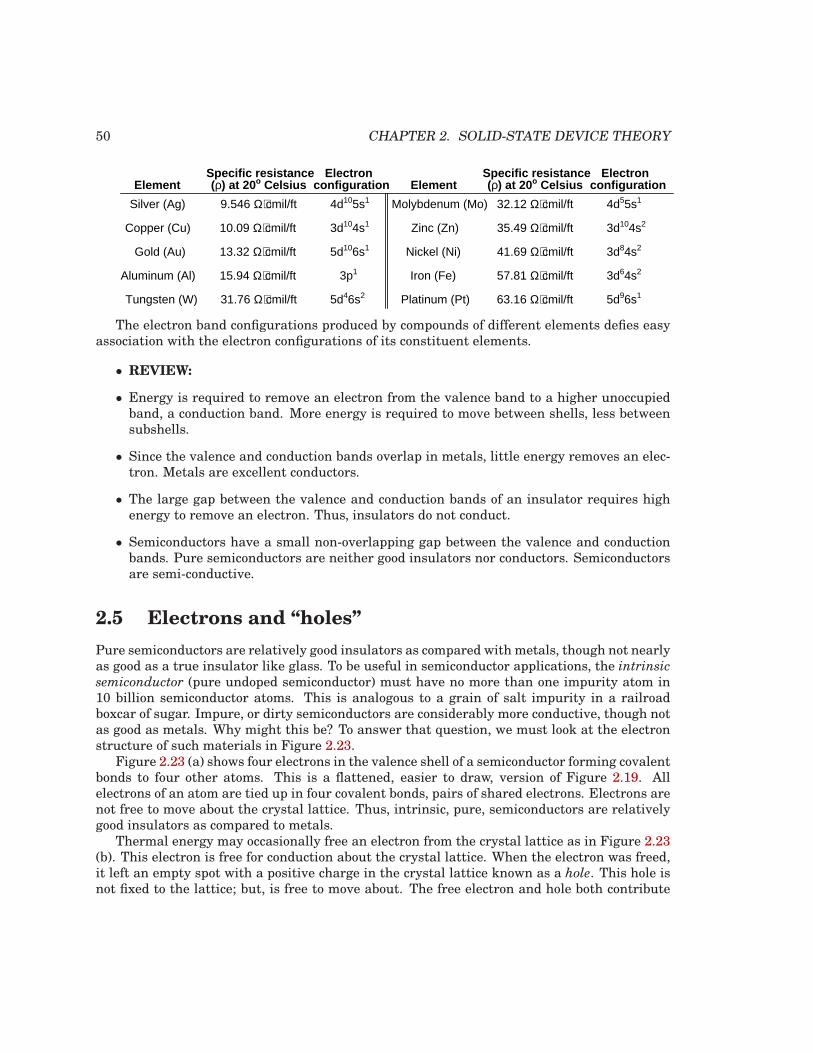
50 CHAPTER 2. SOLID-STATE DEVICE THEORY
ElementSpecific resistance
Silver (Ag)
(ρ) at 20o Celsius
9.546 Ω⋅cmil/ft 4d105s1
Electronconfiguration
Copper (Cu) 10.09 Ω⋅cmil/ft 3d104s1
Gold (Au) 13.32 Ω⋅cmil/ft 5d106s1
Aluminum (Al) 15.94 Ω⋅cmil/ft 3p1
Tungsten (W) 31.76 Ω⋅cmil/ft 5d46s2
Molybdenum (Mo) 32.12 Ω⋅cmil/ft 4d55s1
Zinc (Zn) 35.49 Ω⋅cmil/ft 3d104s2
Nickel (Ni) 41.69 Ω⋅cmil/ft 3d84s2
Iron (Fe) 57.81 Ω⋅cmil/ft 3d64s2
Platinum (Pt) 63.16 Ω⋅cmil/ft 5d96s1
ElementSpecific resistance(ρ) at 20o Celsius
Electronconfiguration
The electron band configurations produced by compounds of different elements defies easyassociation with the electron configurations of its constituent elements.
• REVIEW:
• Energy is required to remove an electron from the valence band to a higher unoccupiedband, a conduction band. More energy is required to move between shells, less betweensubshells.
• Since the valence and conduction bands overlap in metals, little energy removes an elec-tron. Metals are excellent conductors.
• The large gap between the valence and conduction bands of an insulator requires highenergy to remove an electron. Thus, insulators do not conduct.
• Semiconductors have a small non-overlapping gap between the valence and conductionbands. Pure semiconductors are neither good insulators nor conductors. Semiconductorsare semi-conductive.
2.5 Electrons and “holes”
Pure semiconductors are relatively good insulators as compared with metals, though not nearlyas good as a true insulator like glass. To be useful in semiconductor applications, the intrinsic
semiconductor (pure undoped semiconductor) must have no more than one impurity atom in10 billion semiconductor atoms. This is analogous to a grain of salt impurity in a railroadboxcar of sugar. Impure, or dirty semiconductors are considerably more conductive, though notas good as metals. Why might this be? To answer that question, we must look at the electronstructure of such materials in Figure 2.23.
Figure 2.23 (a) shows four electrons in the valence shell of a semiconductor forming covalentbonds to four other atoms. This is a flattened, easier to draw, version of Figure 2.19. Allelectrons of an atom are tied up in four covalent bonds, pairs of shared electrons. Electrons arenot free to move about the crystal lattice. Thus, intrinsic, pure, semiconductors are relativelygood insulators as compared to metals.
Thermal energy may occasionally free an electron from the crystal lattice as in Figure 2.23(b). This electron is free for conduction about the crystal lattice. When the electron was freed,it left an empty spot with a positive charge in the crystal lattice known as a hole. This hole isnot fixed to the lattice; but, is free to move about. The free electron and hole both contribute
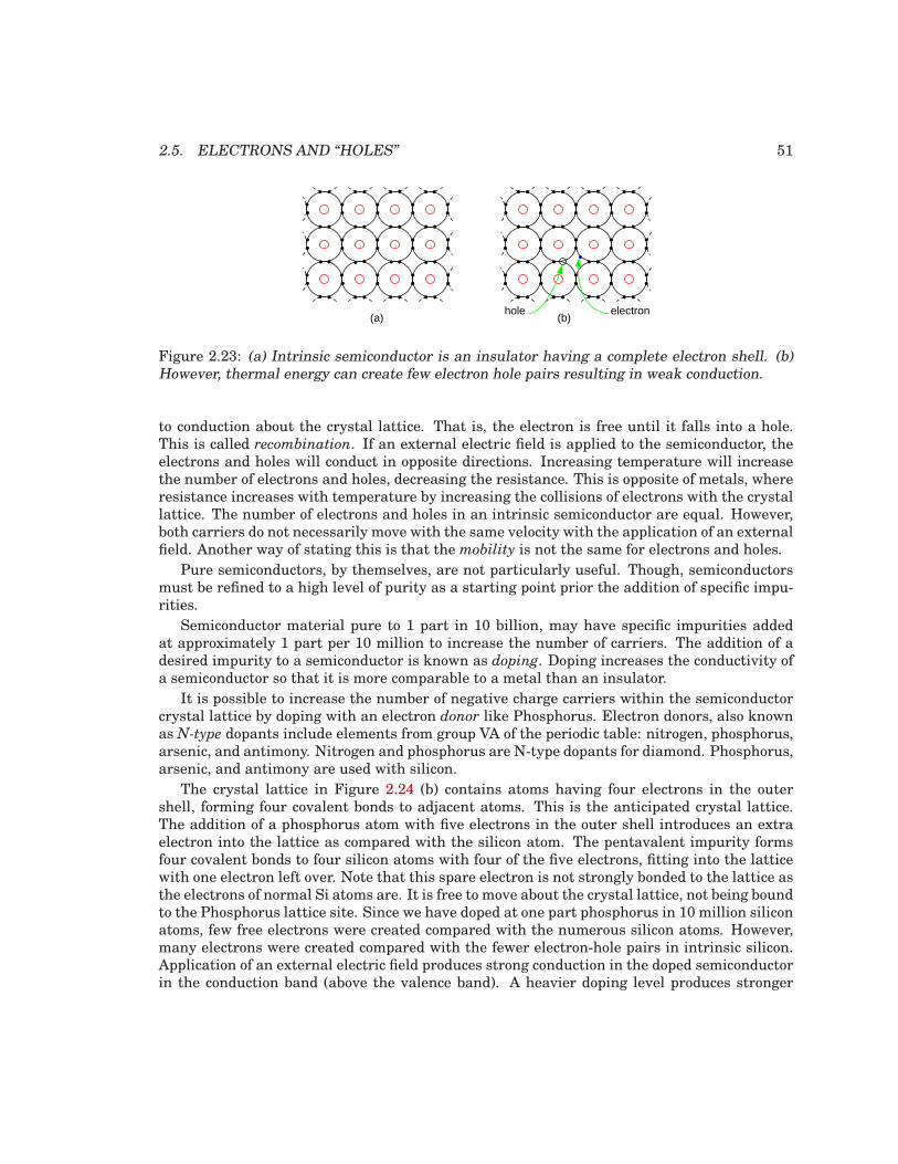
2.5. ELECTRONS AND “HOLES” 51
(b)(a)hole electron
Figure 2.23: (a) Intrinsic semiconductor is an insulator having a complete electron shell. (b)However, thermal energy can create few electron hole pairs resulting in weak conduction.
to conduction about the crystal lattice. That is, the electron is free until it falls into a hole.This is called recombination. If an external electric field is applied to the semiconductor, theelectrons and holes will conduct in opposite directions. Increasing temperature will increasethe number of electrons and holes, decreasing the resistance. This is opposite of metals, whereresistance increases with temperature by increasing the collisions of electrons with the crystallattice. The number of electrons and holes in an intrinsic semiconductor are equal. However,both carriers do not necessarily move with the same velocity with the application of an externalfield. Another way of stating this is that the mobility is not the same for electrons and holes.
Pure semiconductors, by themselves, are not particularly useful. Though, semiconductorsmust be refined to a high level of purity as a starting point prior the addition of specific impu-rities.
Semiconductor material pure to 1 part in 10 billion, may have specific impurities addedat approximately 1 part per 10 million to increase the number of carriers. The addition of adesired impurity to a semiconductor is known as doping. Doping increases the conductivity ofa semiconductor so that it is more comparable to a metal than an insulator.
It is possible to increase the number of negative charge carriers within the semiconductorcrystal lattice by doping with an electron donor like Phosphorus. Electron donors, also knownas N-type dopants include elements from group VA of the periodic table: nitrogen, phosphorus,arsenic, and antimony. Nitrogen and phosphorus are N-type dopants for diamond. Phosphorus,arsenic, and antimony are used with silicon.
The crystal lattice in Figure 2.24 (b) contains atoms having four electrons in the outershell, forming four covalent bonds to adjacent atoms. This is the anticipated crystal lattice.The addition of a phosphorus atom with five electrons in the outer shell introduces an extraelectron into the lattice as compared with the silicon atom. The pentavalent impurity formsfour covalent bonds to four silicon atoms with four of the five electrons, fitting into the latticewith one electron left over. Note that this spare electron is not strongly bonded to the lattice asthe electrons of normal Si atoms are. It is free to move about the crystal lattice, not being boundto the Phosphorus lattice site. Since we have doped at one part phosphorus in 10 million siliconatoms, few free electrons were created compared with the numerous silicon atoms. However,many electrons were created compared with the fewer electron-hole pairs in intrinsic silicon.Application of an external electric field produces strong conduction in the doped semiconductorin the conduction band (above the valence band). A heavier doping level produces stronger
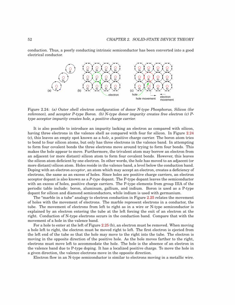
52 CHAPTER 2. SOLID-STATE DEVICE THEORY
conduction. Thus, a poorly conducting intrinsic semiconductor has been converted into a goodelectrical conductor.
(c)(b)
hole movementelectronmovement
P
Si Si SiSi
Si SiSi
Si Si SiSi Si Si SiSi
Si SiSi
Si Si SiSi
BSi
P
B
(a)holeelectron
Figure 2.24: (a) Outer shell electron configuration of donor N-type Phosphorus, Silicon (forreference), and acceptor P-type Boron. (b) N-type donor impurity creates free electron (c) P-type acceptor impurity creates hole, a positive charge carrier.
It is also possible to introduce an impurity lacking an electron as compared with silicon,having three electrons in the valence shell as compared with four for silicon. In Figure 2.24(c), this leaves an empty spot known as a hole, a positive charge carrier. The boron atom triesto bond to four silicon atoms, but only has three electrons in the valence band. In attemptingto form four covalent bonds the three electrons move around trying to form four bonds. Thismakes the hole appear to move. Furthermore, the trivalent atom may borrow an electron froman adjacent (or more distant) silicon atom to form four covalent bonds. However, this leavesthe silicon atom deficient by one electron. In other words, the hole has moved to an adjacent (ormore distant) silicon atom. Holes reside in the valence band, a level below the conduction band.Doping with an electron acceptor, an atom which may accept an electron, creates a deficiency ofelectrons, the same as an excess of holes. Since holes are positive charge carriers, an electronacceptor dopant is also known as a P-type dopant. The P-type dopant leaves the semiconductorwith an excess of holes, positive charge carriers. The P-type elements from group IIIA of theperiodic table include: boron, aluminum, gallium, and indium. Boron is used as a P-typedopant for silicon and diamond semiconductors, while indium is used with germanium.
The “marble in a tube” analogy to electron conduction in Figure 2.25 relates the movementof holes with the movement of electrons. The marble represent electrons in a conductor, thetube. The movement of electrons from left to right as in a wire or N-type semiconductor isexplained by an electron entering the tube at the left forcing the exit of an electron at theright. Conduction of N-type electrons occurs in the conduction band. Compare that with themovement of a hole in the valence band.
For a hole to enter at the left of Figure 2.25 (b), an electron must be removed. When movinga hole left to right, the electron must be moved right to left. The first electron is ejected fromthe left end of the tube so that the hole may move to the right into the tube. The electron ismoving in the opposite direction of the positive hole. As the hole moves farther to the right,electrons must move left to accommodate the hole. The hole is the absence of an electron inthe valence band due to P-type doping. It has a localized positive charge. To move the hole ina given direction, the valence electrons move in the opposite direction.
Electron flow in an N-type semiconductor is similar to electrons moving in a metallic wire.
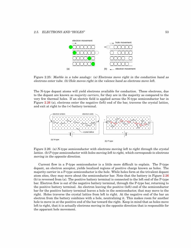
2.5. ELECTRONS AND “HOLES” 53
(a)
electron movementhole movement
electron movement(b)
Figure 2.25: Marble in a tube analogy: (a) Electrons move right in the conduction band aselectrons enter tube. (b) Hole moves right in the valence band as electrons move left.
The N-type dopant atoms will yield electrons available for conduction. These electrons, dueto the dopant are known as majority carriers, for they are in the majority as compared to thevery few thermal holes. If an electric field is applied across the N-type semiconductor bar inFigure 2.26 (a), electrons enter the negative (left) end of the bar, traverse the crystal lattice,and exit at right to the (+) battery terminal.
electron enters electron exits
(a) N-type(b) P-type
crystal lattice
Figure 2.26: (a) N-type semiconductor with electrons moving left to right through the crystallattice. (b) P-type semiconductor with holes moving left to right, which corresponds to electronsmoving in the opposite direction.
Current flow in a P-type semiconductor is a little more difficult to explain. The P-typedopant, an electron acceptor, yields localized regions of positive charge known as holes. Themajority carrier in a P-type semiconductor is the hole. While holes form at the trivalent dopantatom sites, they may move about the semiconductor bar. Note that the battery in Figure 2.26(b) is reversed from (a). The positive battery terminal is connected to the left end of the P-typebar. Electron flow is out of the negative battery terminal, through the P-type bar, returning tothe positive battery terminal. An electron leaving the positive (left) end of the semiconductorbar for the positive battery terminal leaves a hole in the semiconductor, that may move to theright. Holes traverse the crystal lattice from left to right. At the negative end of the bar anelectron from the battery combines with a hole, neutralizing it. This makes room for anotherhole to move in at the positive end of the bar toward the right. Keep in mind that as holes moveleft to right, that it is actually electrons moving in the opposite direction that is responsible forthe apparant hole movement.
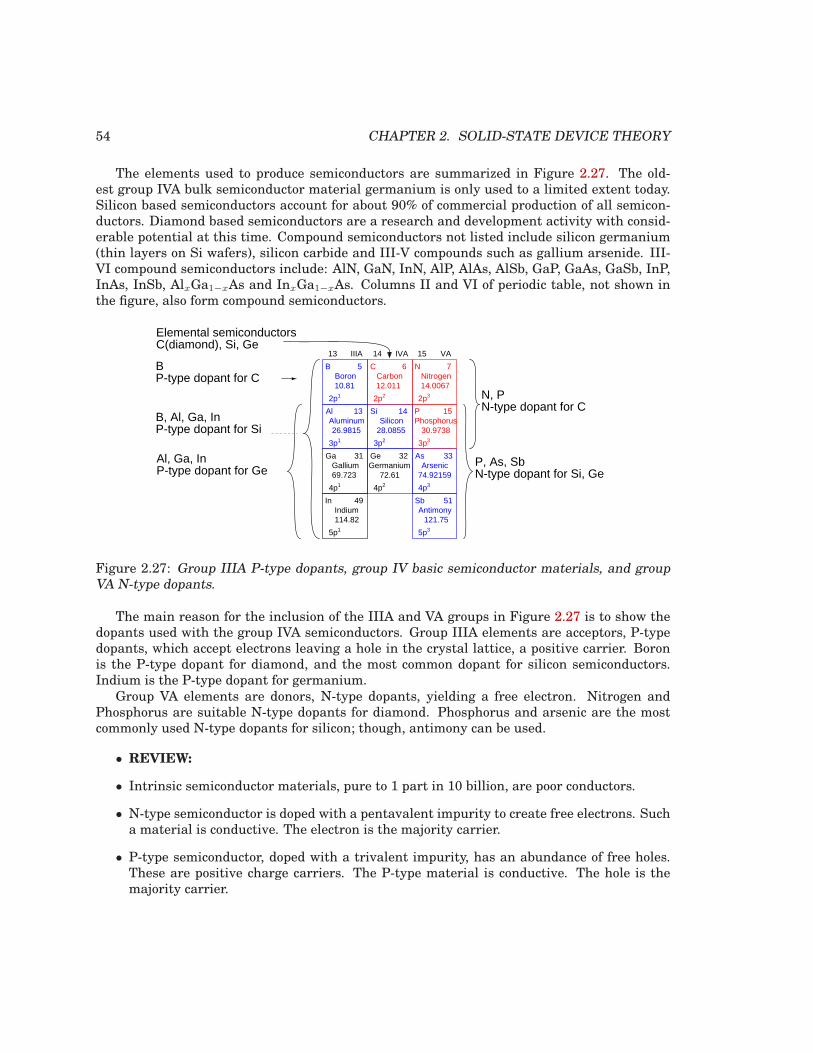
54 CHAPTER 2. SOLID-STATE DEVICE THEORY
The elements used to produce semiconductors are summarized in Figure 2.27. The old-est group IVA bulk semiconductor material germanium is only used to a limited extent today.Silicon based semiconductors account for about 90% of commercial production of all semicon-ductors. Diamond based semiconductors are a research and development activity with consid-erable potential at this time. Compound semiconductors not listed include silicon germanium(thin layers on Si wafers), silicon carbide and III-V compounds such as gallium arsenide. III-VI compound semiconductors include: AlN, GaN, InN, AlP, AlAs, AlSb, GaP, GaAs, GaSb, InP,InAs, InSb, AlxGa1−xAs and InxGa1−xAs. Columns II and VI of periodic table, not shown inthe figure, also form compound semiconductors.
Ga 31Gallium
4p1
B 5Boron10.81
2p1
C 6Carbon12.011
2p2
N 7Nitrogen14.0067
2p3
Al 13Aluminum26.9815
3p1
Si 14Silicon
28.0855
3p2
P 15Phosphorus
30.9738
3p3
Germanium
4p2
Ge 32 AsArsenic
33
4p3
In 49Indium114.82
5p1
Sb 51Antimony
121.75
5p3
69.723 72.61 74.92159
IIIA13 IVA14 VA15
N, PN-type dopant for C
P, As, SbN-type dopant for Si, Ge
BP-type dopant for C
Al, Ga, InP-type dopant for Ge
Elemental semiconductors C(diamond), Si, Ge
B, Al, Ga, InP-type dopant for Si
Figure 2.27: Group IIIA P-type dopants, group IV basic semiconductor materials, and groupVA N-type dopants.
The main reason for the inclusion of the IIIA and VA groups in Figure 2.27 is to show thedopants used with the group IVA semiconductors. Group IIIA elements are acceptors, P-typedopants, which accept electrons leaving a hole in the crystal lattice, a positive carrier. Boronis the P-type dopant for diamond, and the most common dopant for silicon semiconductors.Indium is the P-type dopant for germanium.
Group VA elements are donors, N-type dopants, yielding a free electron. Nitrogen andPhosphorus are suitable N-type dopants for diamond. Phosphorus and arsenic are the mostcommonly used N-type dopants for silicon; though, antimony can be used.
• REVIEW:
• Intrinsic semiconductor materials, pure to 1 part in 10 billion, are poor conductors.
• N-type semiconductor is doped with a pentavalent impurity to create free electrons. Sucha material is conductive. The electron is the majority carrier.
• P-type semiconductor, doped with a trivalent impurity, has an abundance of free holes.These are positive charge carriers. The P-type material is conductive. The hole is themajority carrier.
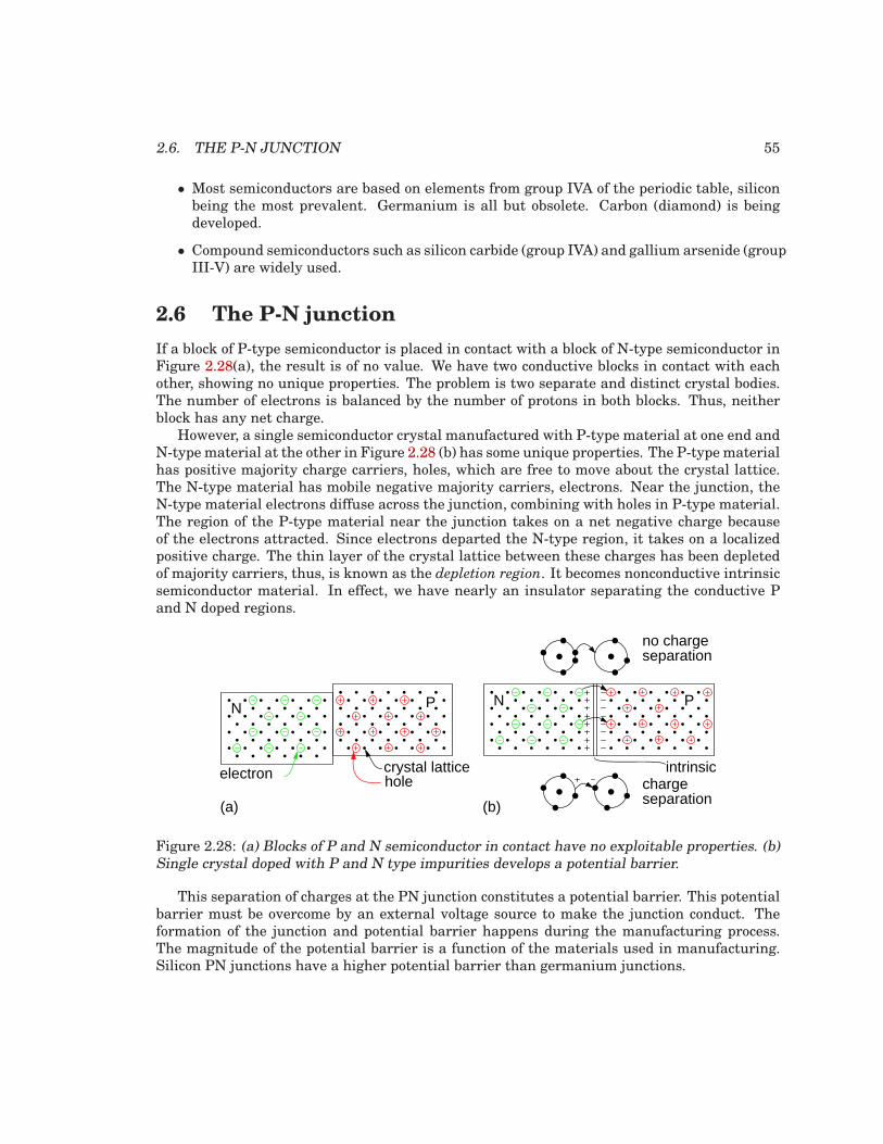
2.6. THE P-N JUNCTION 55
• Most semiconductors are based on elements from group IVA of the periodic table, siliconbeing the most prevalent. Germanium is all but obsolete. Carbon (diamond) is beingdeveloped.
• Compound semiconductors such as silicon carbide (group IVA) and gallium arsenide (groupIII-V) are widely used.
2.6 The P-N junction
If a block of P-type semiconductor is placed in contact with a block of N-type semiconductor inFigure 2.28(a), the result is of no value. We have two conductive blocks in contact with eachother, showing no unique properties. The problem is two separate and distinct crystal bodies.The number of electrons is balanced by the number of protons in both blocks. Thus, neitherblock has any net charge.
However, a single semiconductor crystal manufactured with P-type material at one end andN-type material at the other in Figure 2.28 (b) has some unique properties. The P-type materialhas positive majority charge carriers, holes, which are free to move about the crystal lattice.The N-type material has mobile negative majority carriers, electrons. Near the junction, theN-type material electrons diffuse across the junction, combining with holes in P-type material.The region of the P-type material near the junction takes on a net negative charge becauseof the electrons attracted. Since electrons departed the N-type region, it takes on a localizedpositive charge. The thin layer of the crystal lattice between these charges has been depletedof majority carriers, thus, is known as the depletion region. It becomes nonconductive intrinsicsemiconductor material. In effect, we have nearly an insulator separating the conductive Pand N doped regions.
(a)
crystal lattice
N PN P
(b)
intrinsic
no chargeseparation
chargeseparation
holeelectron
Figure 2.28: (a) Blocks of P and N semiconductor in contact have no exploitable properties. (b)Single crystal doped with P and N type impurities develops a potential barrier.
This separation of charges at the PN junction constitutes a potential barrier. This potentialbarrier must be overcome by an external voltage source to make the junction conduct. Theformation of the junction and potential barrier happens during the manufacturing process.The magnitude of the potential barrier is a function of the materials used in manufacturing.Silicon PN junctions have a higher potential barrier than germanium junctions.
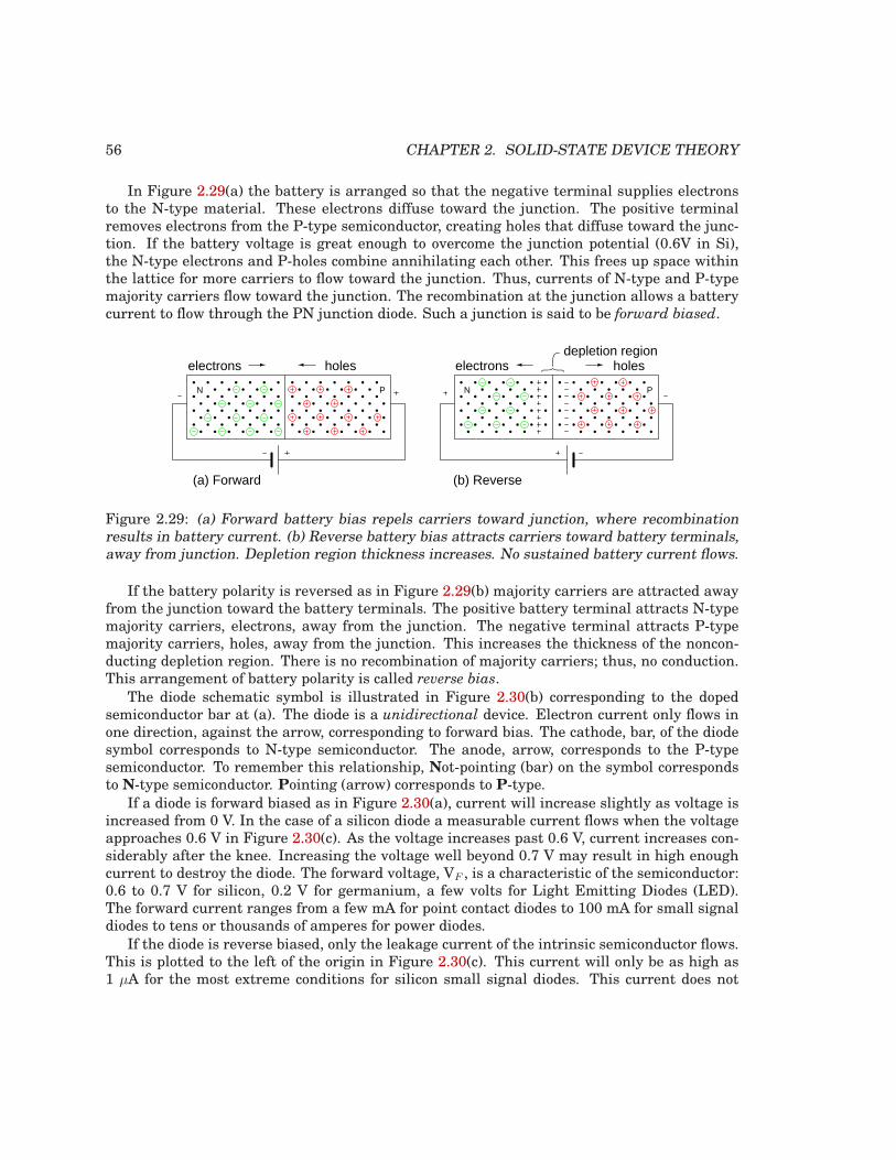
56 CHAPTER 2. SOLID-STATE DEVICE THEORY
In Figure 2.29(a) the battery is arranged so that the negative terminal supplies electronsto the N-type material. These electrons diffuse toward the junction. The positive terminalremoves electrons from the P-type semiconductor, creating holes that diffuse toward the junc-tion. If the battery voltage is great enough to overcome the junction potential (0.6V in Si),the N-type electrons and P-holes combine annihilating each other. This frees up space withinthe lattice for more carriers to flow toward the junction. Thus, currents of N-type and P-typemajority carriers flow toward the junction. The recombination at the junction allows a batterycurrent to flow through the PN junction diode. Such a junction is said to be forward biased.
PN PN
(a) Forward (b) Reverse
depletion regionelectrons holes electrons holes
Figure 2.29: (a) Forward battery bias repels carriers toward junction, where recombinationresults in battery current. (b) Reverse battery bias attracts carriers toward battery terminals,away from junction. Depletion region thickness increases. No sustained battery current flows.
If the battery polarity is reversed as in Figure 2.29(b) majority carriers are attracted awayfrom the junction toward the battery terminals. The positive battery terminal attracts N-typemajority carriers, electrons, away from the junction. The negative terminal attracts P-typemajority carriers, holes, away from the junction. This increases the thickness of the noncon-ducting depletion region. There is no recombination of majority carriers; thus, no conduction.This arrangement of battery polarity is called reverse bias.
The diode schematic symbol is illustrated in Figure 2.30(b) corresponding to the dopedsemiconductor bar at (a). The diode is a unidirectional device. Electron current only flows inone direction, against the arrow, corresponding to forward bias. The cathode, bar, of the diodesymbol corresponds to N-type semiconductor. The anode, arrow, corresponds to the P-typesemiconductor. To remember this relationship, Not-pointing (bar) on the symbol correspondsto N-type semiconductor. Pointing (arrow) corresponds to P-type.
If a diode is forward biased as in Figure 2.30(a), current will increase slightly as voltage isincreased from 0 V. In the case of a silicon diode a measurable current flows when the voltageapproaches 0.6 V in Figure 2.30(c). As the voltage increases past 0.6 V, current increases con-siderably after the knee. Increasing the voltage well beyond 0.7 V may result in high enoughcurrent to destroy the diode. The forward voltage, VF , is a characteristic of the semiconductor:0.6 to 0.7 V for silicon, 0.2 V for germanium, a few volts for Light Emitting Diodes (LED).The forward current ranges from a few mA for point contact diodes to 100 mA for small signaldiodes to tens or thousands of amperes for power diodes.
If the diode is reverse biased, only the leakage current of the intrinsic semiconductor flows.This is plotted to the left of the origin in Figure 2.30(c). This current will only be as high as1 µA for the most extreme conditions for silicon small signal diodes. This current does not
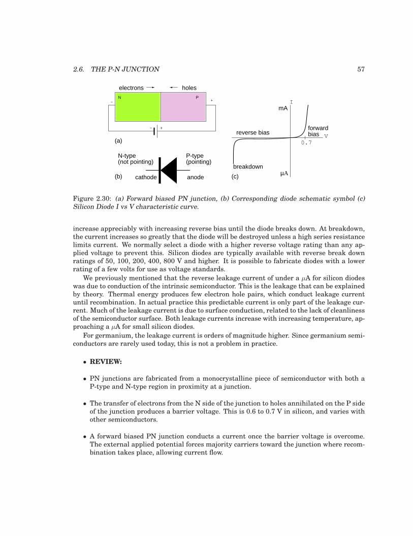
2.6. THE P-N JUNCTION 57
(a)
(c)
electrons holes
(b) cathode anode
P-type(pointing)
N-type(not pointing)
0.7V
I
reverse biasforwardbias
mA
µAbreakdown
PN
Figure 2.30: (a) Forward biased PN junction, (b) Corresponding diode schematic symbol (c)Silicon Diode I vs V characteristic curve.
increase appreciably with increasing reverse bias until the diode breaks down. At breakdown,the current increases so greatly that the diode will be destroyed unless a high series resistancelimits current. We normally select a diode with a higher reverse voltage rating than any ap-plied voltage to prevent this. Silicon diodes are typically available with reverse break downratings of 50, 100, 200, 400, 800 V and higher. It is possible to fabricate diodes with a lowerrating of a few volts for use as voltage standards.
We previously mentioned that the reverse leakage current of under a µA for silicon diodeswas due to conduction of the intrinsic semiconductor. This is the leakage that can be explainedby theory. Thermal energy produces few electron hole pairs, which conduct leakage currentuntil recombination. In actual practice this predictable current is only part of the leakage cur-rent. Much of the leakage current is due to surface conduction, related to the lack of cleanlinessof the semiconductor surface. Both leakage currents increase with increasing temperature, ap-proaching a µA for small silicon diodes.
For germanium, the leakage current is orders of magnitude higher. Since germanium semi-conductors are rarely used today, this is not a problem in practice.
• REVIEW:
• PN junctions are fabricated from a monocrystalline piece of semiconductor with both aP-type and N-type region in proximity at a junction.
• The transfer of electrons from the N side of the junction to holes annihilated on the P sideof the junction produces a barrier voltage. This is 0.6 to 0.7 V in silicon, and varies withother semiconductors.
• A forward biased PN junction conducts a current once the barrier voltage is overcome.The external applied potential forces majority carriers toward the junction where recom-bination takes place, allowing current flow.
58 CHAPTER 2. SOLID-STATE DEVICE THEORY
• A reverse biased PN junction conducts almost no current. The applied reverse bias at-tracts majority carriers away from the junction. This increases the thickness of the non-conducting depletion region.
• Reverse biased PN junctions show a temperature dependent reverse leakage current.This is less than a µA in small silicon diodes.
2.7 Junction diodes
There were some historic crude, but usable semiconductor rectifiers before high purity materi-als were available. Ferdinand Braun invented a lead sulfide, PbS, based point contact rectifierin 1874. Cuprous oxide rectifiers were used as power rectifiers in 1924. The forward voltagedrop is 0.2 V. The linear characteristic curve perhaps is why Cu2O was used as a rectifier forthe AC scale on D’Arsonval based multimeters. This diode is also photosensitive.
Selenium oxide rectifiers were used before modern power diode rectifiers became available.These and the Cu2O rectifiers were polycrystalline devices. Photoelectric cells were once madefrom Selenium.
Before the modern semiconductor era, an early diode application was as a radio frequencydetector, which recovered audio from a radio signal. The “semiconductor” was a polycrystallinepiece of the mineral galena, lead sulfide, PbS. A pointed metallic wire known as a cat whisker
was brought in contact with a spot on a crystal within the polycrystalline mineral. (Figure 2.31)The operator labored to find a “sensitive” spot on the galena by moving the cat whisker about.Presumably there were P and N-type spots randomly distributed throughout the crystal dueto the variability of uncontrolled impurities. Less often the mineral iron pyrites, fools gold,was used, as was the mineral carborundum, silicon carbide, SiC, another detector, part of afoxhole radio, consisted of a sharpened pencil lead bound to a bent safety pin, touching a rustyblue-blade disposable razor blade. These all required searching for a sensitive spot, easily lostbecause of vibration.
Replacing the mineral with an N-doped semiconductor (Figure 2.32(a) ) makes the wholesurface sensitive, so that searching for a sensitive spot was no longer required. This device wasperfected by G.W.Pickard in 1906. The pointed metal contact produced a localized P-type regionwithin the semiconductor. The metal point was fixed in place, and the whole point contact diodeencapsulated in a cylindrical body for mechanical and electrical stability. (Figure 2.32(d) ) Notethat the cathode bar on the schematic corresponds to the bar on the physical package.
Silicon point contact diodes made an important contribution to radar in World War II, de-tecting giga-hertz radio frequency echo signals in the radar receiver. The concept to be madeclear is that the point contact diode preceded the junction diode and modern semiconductorsby several decades. Even to this day, the point contact diode is a practical means of microwavefrequency detection because of its low capacitance. Germanium point contact diodes were oncemore readily available than they are today, being preferred for the lower 0.2 V forward voltagein some applications like self-powered crystal radios. Point contact diodes, though sensitive toa wide bandwidth, have a low current capability compared with junction diodes.
Most diodes today are silicon junction diodes. The cross-section in Figure 2.32(b) looks abit more complex than a simple PN junction; though, it is still a PN junction. Starting at thecathode connection, the N+ indicates this region is heavily doped, having nothing to do with
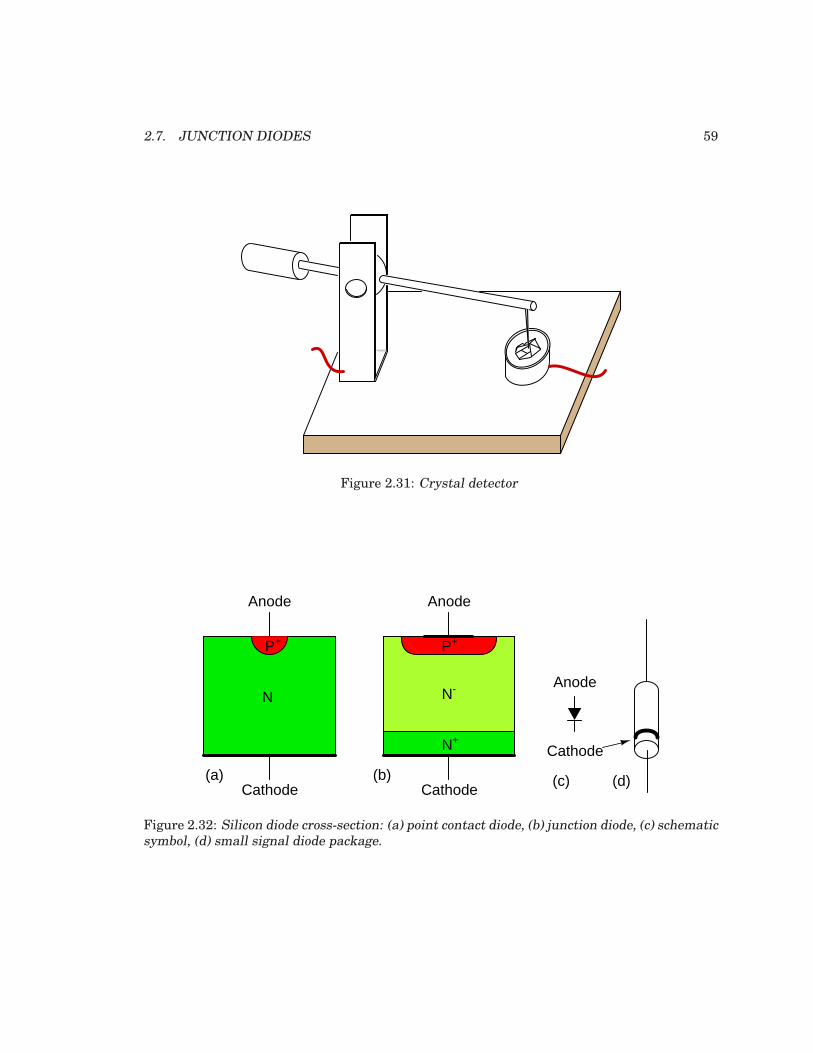
2.7. JUNCTION DIODES 59
Figure 2.31: Crystal detector
Anode
Cathode
Cathode
Anode
Anode
Cathode(a) (b) (c) (d)
P+
N
P+
N-
N+
Figure 2.32: Silicon diode cross-section: (a) point contact diode, (b) junction diode, (c) schematicsymbol, (d) small signal diode package.
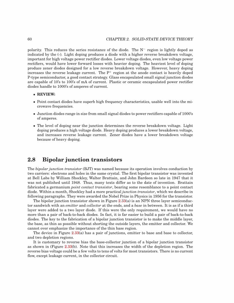
60 CHAPTER 2. SOLID-STATE DEVICE THEORY
polarity. This reduces the series resistance of the diode. The N− region is lightly doped asindicated by the (-). Light doping produces a diode with a higher reverse breakdown voltage,important for high voltage power rectifier diodes. Lower voltage diodes, even low voltage powerrectifiers, would have lower forward losses with heavier doping. The heaviest level of dopingproduce zener diodes designed for a low reverse breakdown voltage. However, heavy dopingincreases the reverse leakage current. The P+ region at the anode contact is heavily dopedP-type semiconductor, a good contact strategy. Glass encapsulated small signal junction diodesare capable of 10’s to 100’s of mA of current. Plastic or ceramic encapsulated power rectifierdiodes handle to 1000’s of amperes of current.
• REVIEW:
• Point contact diodes have superb high frequency characteristics, usable well into the mi-crowave frequencies.
• Junction diodes range in size from small signal diodes to power rectifiers capable of 1000’sof amperes.
• The level of doping near the junction determines the reverse breakdown voltage. Lightdoping produces a high voltage diode. Heavy doping produces a lower breakdown voltage,and increases reverse leakage current. Zener diodes have a lower breakdown voltagebecause of heavy doping.
2.8 Bipolar junction transistors
The bipolar junction transistor (BJT) was named because its operation involves conduction bytwo carriers: electrons and holes in the same crystal. The first bipolar transistor was inventedat Bell Labs by William Shockley, Walter Brattain, and John Bardeen so late in 1947 that itwas not published until 1948. Thus, many texts differ as to the date of invention. Brattainfabricated a germanium point contact transistor, bearing some resemblance to a point contactdiode. Within a month, Shockley had a more practical junction transistor, which we describe infollowing paragraphs. They were awarded the Nobel Prize in Physics in 1956 for the transistor.
The bipolar junction transistor shown in Figure 2.33(a) is an NPN three layer semiconduc-tor sandwich with an emitter and collector at the ends, and a base in between. It is as if a thirdlayer were added to a two layer diode. If this were the only requirement, we would have nomore than a pair of back-to-back diodes. In fact, it is far easier to build a pair of back-to-backdiodes. The key to the fabrication of a bipolar junction transistor is to make the middle layer,the base, as thin as possible without shorting the outside layers, the emitter and collector. Wecannot over emphasize the importance of the thin base region.
The device in Figure 2.33(a) has a pair of junctions, emitter to base and base to collector,and two depletion regions.
It is customary to reverse bias the base-collector junction of a bipolar junction transistoras shown in (Figure 2.33(b). Note that this increases the width of the depletion region. Thereverse bias voltage could be a few volts to tens of volts for most transistors. There is no currentflow, except leakage current, in the collector circuit.
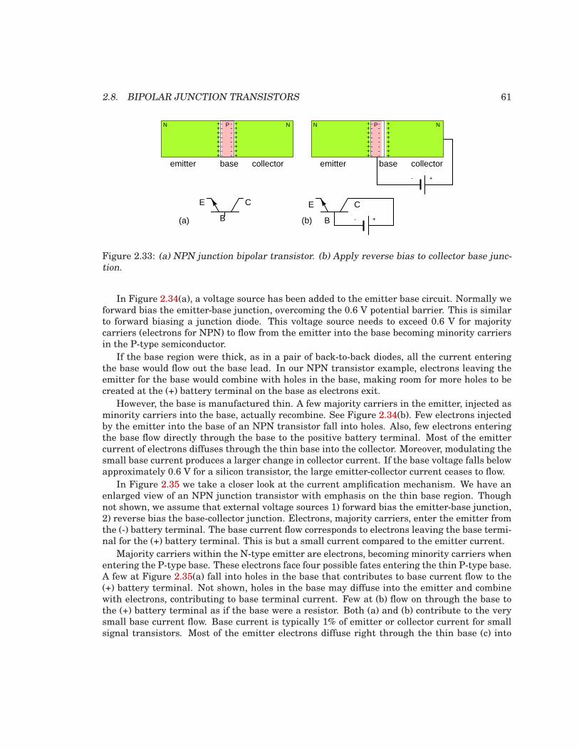
2.8. BIPOLAR JUNCTION TRANSISTORS 61
- +
+-
+-+-
+-
+-+-
+-+-
+
++
+
++
++
--
--
--
--
N NP+-
+-+-
+-
+-+-
+-+-
+
++
+
++
++
--
--
--
--
N NP
(a) (b)
emitter base collector emitter base collector
E
B
C E
B
C
- +
Figure 2.33: (a) NPN junction bipolar transistor. (b) Apply reverse bias to collector base junc-tion.
In Figure 2.34(a), a voltage source has been added to the emitter base circuit. Normally weforward bias the emitter-base junction, overcoming the 0.6 V potential barrier. This is similarto forward biasing a junction diode. This voltage source needs to exceed 0.6 V for majoritycarriers (electrons for NPN) to flow from the emitter into the base becoming minority carriersin the P-type semiconductor.
If the base region were thick, as in a pair of back-to-back diodes, all the current enteringthe base would flow out the base lead. In our NPN transistor example, electrons leaving theemitter for the base would combine with holes in the base, making room for more holes to becreated at the (+) battery terminal on the base as electrons exit.
However, the base is manufactured thin. A few majority carriers in the emitter, injected asminority carriers into the base, actually recombine. See Figure 2.34(b). Few electrons injectedby the emitter into the base of an NPN transistor fall into holes. Also, few electrons enteringthe base flow directly through the base to the positive battery terminal. Most of the emittercurrent of electrons diffuses through the thin base into the collector. Moreover, modulating thesmall base current produces a larger change in collector current. If the base voltage falls belowapproximately 0.6 V for a silicon transistor, the large emitter-collector current ceases to flow.
In Figure 2.35 we take a closer look at the current amplification mechanism. We have anenlarged view of an NPN junction transistor with emphasis on the thin base region. Thoughnot shown, we assume that external voltage sources 1) forward bias the emitter-base junction,2) reverse bias the base-collector junction. Electrons, majority carriers, enter the emitter fromthe (-) battery terminal. The base current flow corresponds to electrons leaving the base termi-nal for the (+) battery terminal. This is but a small current compared to the emitter current.
Majority carriers within the N-type emitter are electrons, becoming minority carriers whenentering the P-type base. These electrons face four possible fates entering the thin P-type base.A few at Figure 2.35(a) fall into holes in the base that contributes to base current flow to the(+) battery terminal. Not shown, holes in the base may diffuse into the emitter and combinewith electrons, contributing to base terminal current. Few at (b) flow on through the base tothe (+) battery terminal as if the base were a resistor. Both (a) and (b) contribute to the verysmall base current flow. Base current is typically 1% of emitter or collector current for smallsignal transistors. Most of the emitter electrons diffuse right through the thin base (c) into
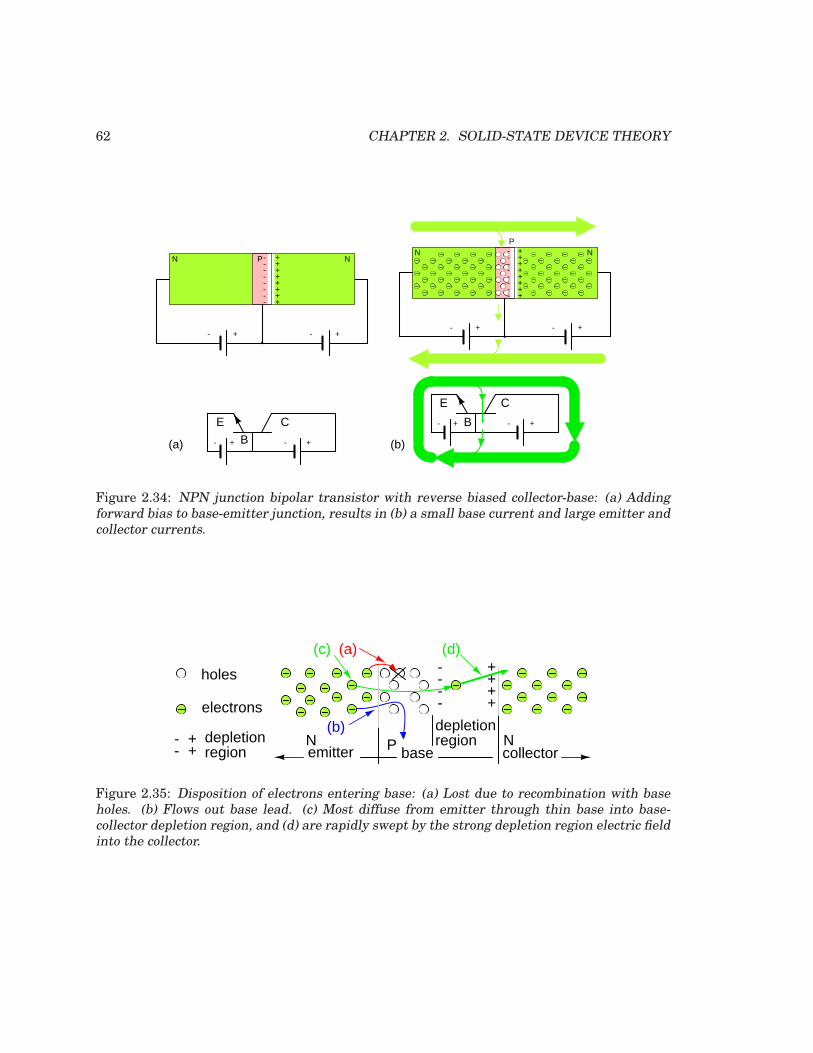
62 CHAPTER 2. SOLID-STATE DEVICE THEORY
(b)
- +
+
++
+
++
++
--
--
--
--
N NP
- +- +
+
++
+
++
++
---
--
--
N NP
- +
-
E
B
C
- +- +(a)
E C
- +- + B
Figure 2.34: NPN junction bipolar transistor with reverse biased collector-base: (a) Addingforward bias to base-emitter junction, results in (b) a small base current and large emitter andcollector currents.
---
P
-
emitter baseN
++
++
collectorN
depletionregion
electrons
holes
(a)(c)
(b)
(d)
- +- +
depletionregion
Figure 2.35: Disposition of electrons entering base: (a) Lost due to recombination with baseholes. (b) Flows out base lead. (c) Most diffuse from emitter through thin base into base-collector depletion region, and (d) are rapidly swept by the strong depletion region electric fieldinto the collector.
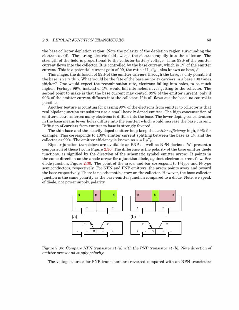
2.8. BIPOLAR JUNCTION TRANSISTORS 63
the base-collector depletion region. Note the polarity of the depletion region surrounding theelectron at (d). The strong electric field sweeps the electron rapidly into the collector. Thestrength of the field is proportional to the collector battery voltage. Thus 99% of the emittercurrent flows into the collector. It is controlled by the base current, which is 1% of the emittercurrent. This is a potential current gain of 99, the ratio of IC /IB , also known as beta, β.
This magic, the diffusion of 99% of the emitter carriers through the base, is only possible ifthe base is very thin. What would be the fate of the base minority carriers in a base 100 timesthicker? One would expect the recombination rate, electrons falling into holes, to be muchhigher. Perhaps 99%, instead of 1%, would fall into holes, never getting to the collector. Thesecond point to make is that the base current may control 99% of the emitter current, only if99% of the emitter current diffuses into the collector. If it all flows out the base, no control ispossible.
Another feature accounting for passing 99% of the electrons from emitter to collector is thatreal bipolar junction transistors use a small heavily doped emitter. The high concentration ofemitter electrons forces many electrons to diffuse into the base. The lower doping concentrationin the base means fewer holes diffuse into the emitter, which would increase the base current.Diffusion of carriers from emitter to base is strongly favored.
The thin base and the heavily doped emitter help keep the emitter efficiency high, 99% forexample. This corresponds to 100% emitter current splitting between the base as 1% and thecollector as 99%. The emitter efficiency is known as α = IC /IE .
Bipolar junction transistors are available as PNP as well as NPN devices. We present acomparison of these two in Figure 2.36. The difference is the polarity of the base emitter diodejunctions, as signified by the direction of the schematic symbol emitter arrow. It points inthe same direction as the anode arrow for a junction diode, against electron current flow. Seediode junction, Figure 2.30. The point of the arrow and bar correspond to P-type and N-typesemiconductors, respectively. For NPN and PNP emitters, the arrow points away and towardthe base respectively. There is no schematic arrow on the collector. However, the base-collectorjunction is the same polarity as the base-emitter junction compared to a diode. Note, we speakof diode, not power supply, polarity.
(a)
- +
N NP
- +
- +- +
(b)
-+
NP
-+
P
-+ -+
E
B
C E
B
C
Figure 2.36: Compare NPN transistor at (a) with the PNP transistor at (b). Note direction ofemitter arrow and supply polarity.
The voltage sources for PNP transistors are reversed compared with an NPN transistors
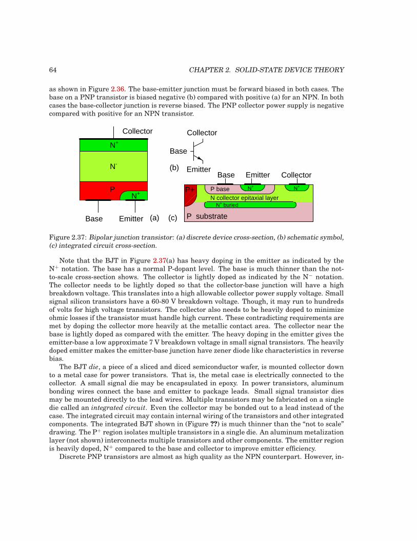
64 CHAPTER 2. SOLID-STATE DEVICE THEORY
as shown in Figure 2.36. The base-emitter junction must be forward biased in both cases. Thebase on a PNP transistor is biased negative (b) compared with positive (a) for an NPN. In bothcases the base-collector junction is reverse biased. The PNP collector power supply is negativecompared with positive for an NPN transistor.
Collector
Emitter
Base
(a)
(b)N-
N+
Collector
Base Emitter
N+P
N+ buriedN collector epitaxial layer
P+ P base
P substrate
N+ N+
Emitter CollectorBase
(c)
Figure 2.37: Bipolar junction transistor: (a) discrete device cross-section, (b) schematic symbol,(c) integrated circuit cross-section.
Note that the BJT in Figure 2.37(a) has heavy doping in the emitter as indicated by theN+ notation. The base has a normal P-dopant level. The base is much thinner than the not-to-scale cross-section shows. The collector is lightly doped as indicated by the N− notation.The collector needs to be lightly doped so that the collector-base junction will have a highbreakdown voltage. This translates into a high allowable collector power supply voltage. Smallsignal silicon transistors have a 60-80 V breakdown voltage. Though, it may run to hundredsof volts for high voltage transistors. The collector also needs to be heavily doped to minimizeohmic losses if the transistor must handle high current. These contradicting requirements aremet by doping the collector more heavily at the metallic contact area. The collector near thebase is lightly doped as compared with the emitter. The heavy doping in the emitter gives theemitter-base a low approximate 7 V breakdown voltage in small signal transistors. The heavilydoped emitter makes the emitter-base junction have zener diode like characteristics in reversebias.
The BJT die, a piece of a sliced and diced semiconductor wafer, is mounted collector downto a metal case for power transistors. That is, the metal case is electrically connected to thecollector. A small signal die may be encapsulated in epoxy. In power transistors, aluminumbonding wires connect the base and emitter to package leads. Small signal transistor diesmay be mounted directly to the lead wires. Multiple transistors may be fabricated on a singledie called an integrated circuit. Even the collector may be bonded out to a lead instead of thecase. The integrated circuit may contain internal wiring of the transistors and other integratedcomponents. The integrated BJT shown in (Figure ??) is much thinner than the “not to scale”drawing. The P+ region isolates multiple transistors in a single die. An aluminummetalizationlayer (not shown) interconnects multiple transistors and other components. The emitter regionis heavily doped, N+ compared to the base and collector to improve emitter efficiency.
Discrete PNP transistors are almost as high quality as the NPN counterpart. However, in-
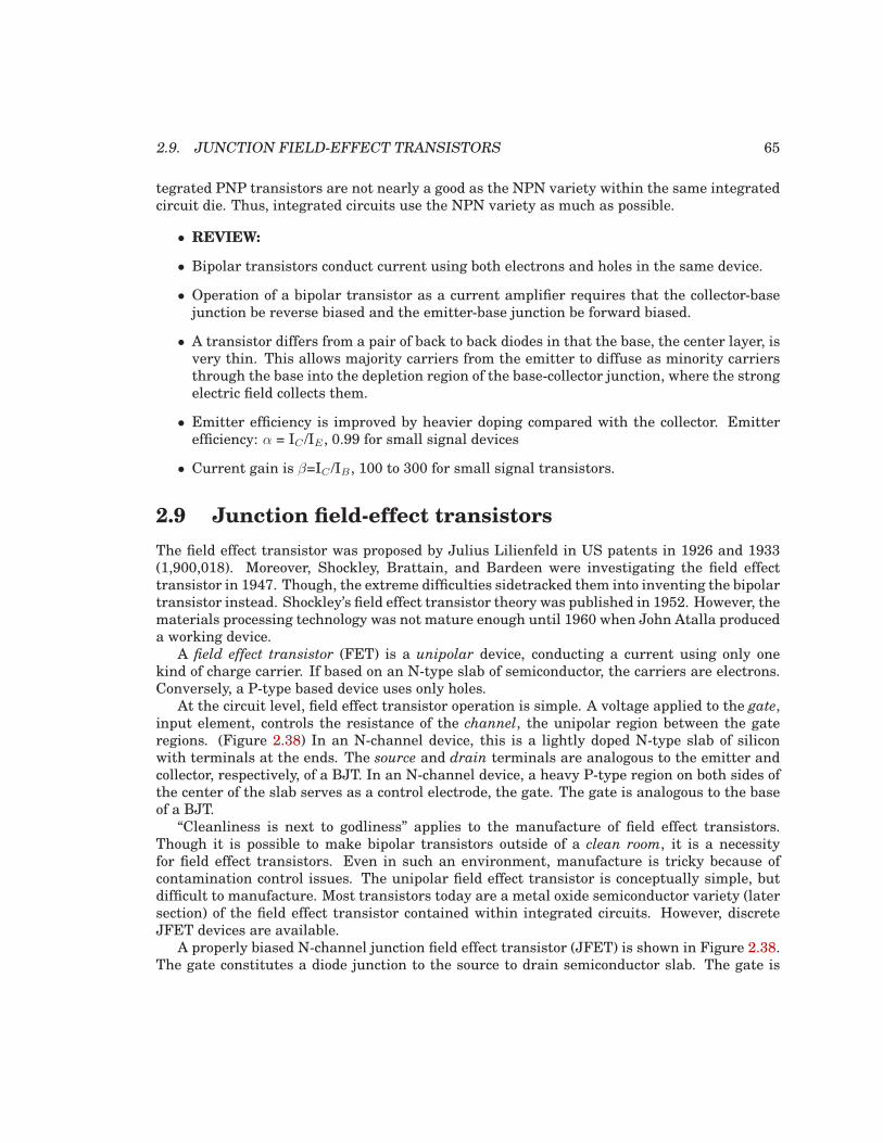
2.9. JUNCTION FIELD-EFFECT TRANSISTORS 65
tegrated PNP transistors are not nearly a good as the NPN variety within the same integratedcircuit die. Thus, integrated circuits use the NPN variety as much as possible.
• REVIEW:
• Bipolar transistors conduct current using both electrons and holes in the same device.
• Operation of a bipolar transistor as a current amplifier requires that the collector-basejunction be reverse biased and the emitter-base junction be forward biased.
• A transistor differs from a pair of back to back diodes in that the base, the center layer, isvery thin. This allows majority carriers from the emitter to diffuse as minority carriersthrough the base into the depletion region of the base-collector junction, where the strongelectric field collects them.
• Emitter efficiency is improved by heavier doping compared with the collector. Emitterefficiency: α = IC /IE , 0.99 for small signal devices
• Current gain is β=IC /IB, 100 to 300 for small signal transistors.
2.9 Junction field-effect transistors
The field effect transistor was proposed by Julius Lilienfeld in US patents in 1926 and 1933(1,900,018). Moreover, Shockley, Brattain, and Bardeen were investigating the field effecttransistor in 1947. Though, the extreme difficulties sidetracked them into inventing the bipolartransistor instead. Shockley’s field effect transistor theory was published in 1952. However, thematerials processing technology was not mature enough until 1960 when John Atalla produceda working device.
A field effect transistor (FET) is a unipolar device, conducting a current using only onekind of charge carrier. If based on an N-type slab of semiconductor, the carriers are electrons.Conversely, a P-type based device uses only holes.
At the circuit level, field effect transistor operation is simple. A voltage applied to the gate,input element, controls the resistance of the channel, the unipolar region between the gateregions. (Figure 2.38) In an N-channel device, this is a lightly doped N-type slab of siliconwith terminals at the ends. The source and drain terminals are analogous to the emitter andcollector, respectively, of a BJT. In an N-channel device, a heavy P-type region on both sides ofthe center of the slab serves as a control electrode, the gate. The gate is analogous to the baseof a BJT.
“Cleanliness is next to godliness” applies to the manufacture of field effect transistors.Though it is possible to make bipolar transistors outside of a clean room, it is a necessityfor field effect transistors. Even in such an environment, manufacture is tricky because ofcontamination control issues. The unipolar field effect transistor is conceptually simple, butdifficult to manufacture. Most transistors today are a metal oxide semiconductor variety (latersection) of the field effect transistor contained within integrated circuits. However, discreteJFET devices are available.
A properly biased N-channel junction field effect transistor (JFET) is shown in Figure 2.38.The gate constitutes a diode junction to the source to drain semiconductor slab. The gate is
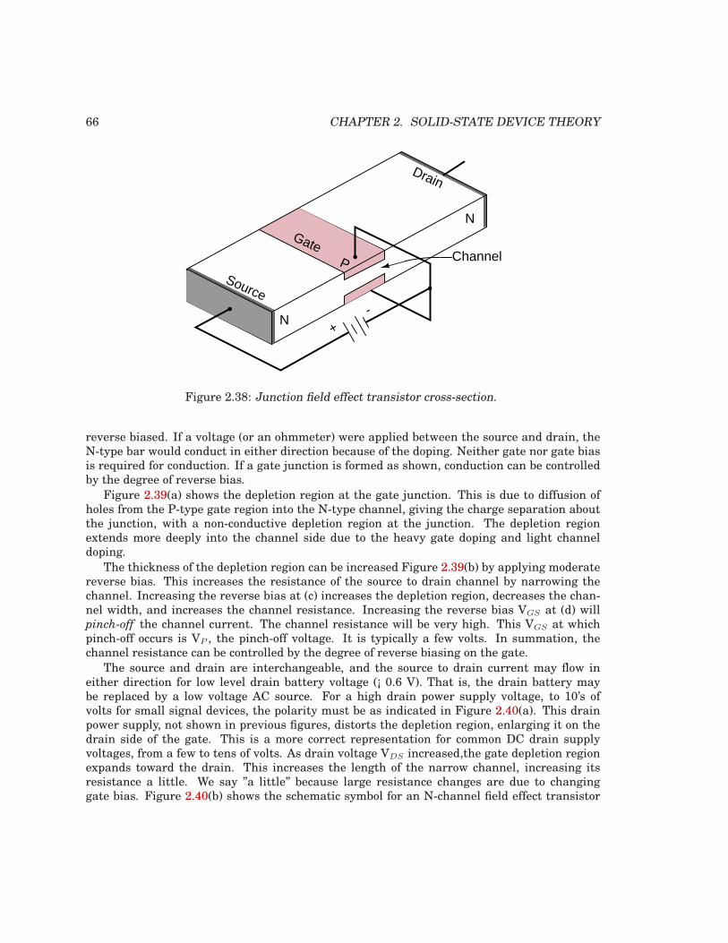
66 CHAPTER 2. SOLID-STATE DEVICE THEORY
Source
Gate
Drain
N
N
P
+-
Channel
Figure 2.38: Junction field effect transistor cross-section.
reverse biased. If a voltage (or an ohmmeter) were applied between the source and drain, theN-type bar would conduct in either direction because of the doping. Neither gate nor gate biasis required for conduction. If a gate junction is formed as shown, conduction can be controlledby the degree of reverse bias.
Figure 2.39(a) shows the depletion region at the gate junction. This is due to diffusion ofholes from the P-type gate region into the N-type channel, giving the charge separation aboutthe junction, with a non-conductive depletion region at the junction. The depletion regionextends more deeply into the channel side due to the heavy gate doping and light channeldoping.
The thickness of the depletion region can be increased Figure 2.39(b) by applying moderatereverse bias. This increases the resistance of the source to drain channel by narrowing thechannel. Increasing the reverse bias at (c) increases the depletion region, decreases the chan-nel width, and increases the channel resistance. Increasing the reverse bias VGS at (d) willpinch-off the channel current. The channel resistance will be very high. This VGS at whichpinch-off occurs is VP , the pinch-off voltage. It is typically a few volts. In summation, thechannel resistance can be controlled by the degree of reverse biasing on the gate.
The source and drain are interchangeable, and the source to drain current may flow ineither direction for low level drain battery voltage (¡ 0.6 V). That is, the drain battery maybe replaced by a low voltage AC source. For a high drain power supply voltage, to 10’s ofvolts for small signal devices, the polarity must be as indicated in Figure 2.40(a). This drainpower supply, not shown in previous figures, distorts the depletion region, enlarging it on thedrain side of the gate. This is a more correct representation for common DC drain supplyvoltages, from a few to tens of volts. As drain voltage VDS increased,the gate depletion regionexpands toward the drain. This increases the length of the narrow channel, increasing itsresistance a little. We say ”a little” because large resistance changes are due to changinggate bias. Figure 2.40(b) shows the schematic symbol for an N-channel field effect transistor
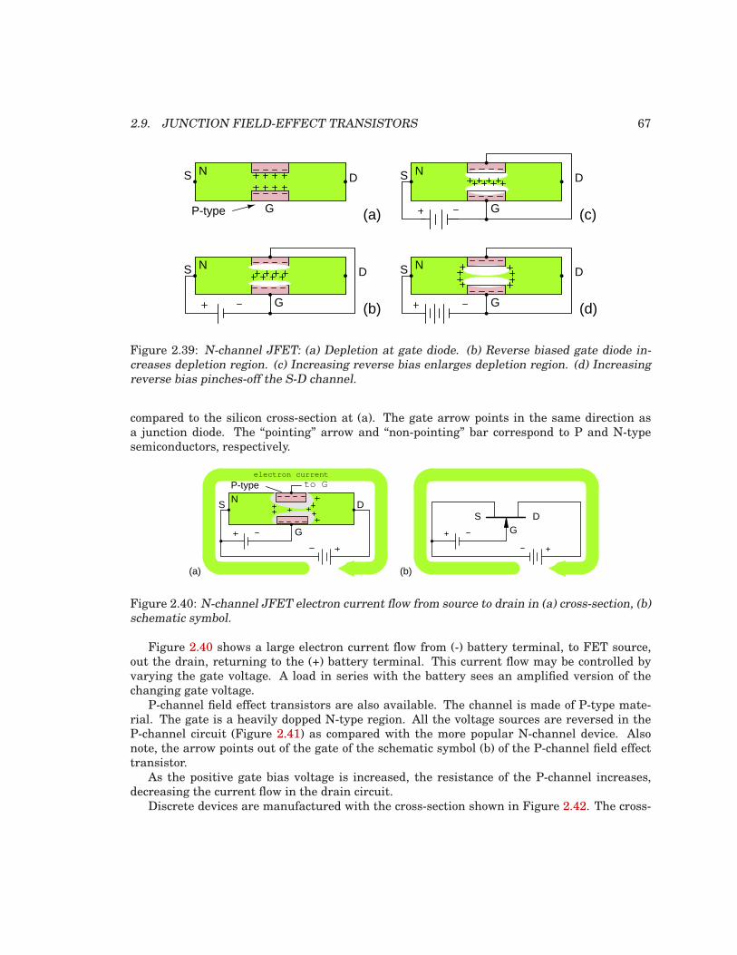
2.9. JUNCTION FIELD-EFFECT TRANSISTORS 67
N
N
N
N
(b)
(a) (c)
(d)
DS
GP-type
S D
S D
S D
G G
G
Figure 2.39: N-channel JFET: (a) Depletion at gate diode. (b) Reverse biased gate diode in-creases depletion region. (c) Increasing reverse bias enlarges depletion region. (d) Increasingreverse bias pinches-off the S-D channel.
compared to the silicon cross-section at (a). The gate arrow points in the same direction asa junction diode. The “pointing” arrow and “non-pointing” bar correspond to P and N-typesemiconductors, respectively.
GG
SS
DD
(a) (b)
electron current
N
to GP-type
Figure 2.40: N-channel JFET electron current flow from source to drain in (a) cross-section, (b)schematic symbol.
Figure 2.40 shows a large electron current flow from (-) battery terminal, to FET source,out the drain, returning to the (+) battery terminal. This current flow may be controlled byvarying the gate voltage. A load in series with the battery sees an amplified version of thechanging gate voltage.
P-channel field effect transistors are also available. The channel is made of P-type mate-rial. The gate is a heavily dopped N-type region. All the voltage sources are reversed in theP-channel circuit (Figure 2.41) as compared with the more popular N-channel device. Alsonote, the arrow points out of the gate of the schematic symbol (b) of the P-channel field effecttransistor.
As the positive gate bias voltage is increased, the resistance of the P-channel increases,decreasing the current flow in the drain circuit.
Discrete devices are manufactured with the cross-section shown in Figure 2.42. The cross-
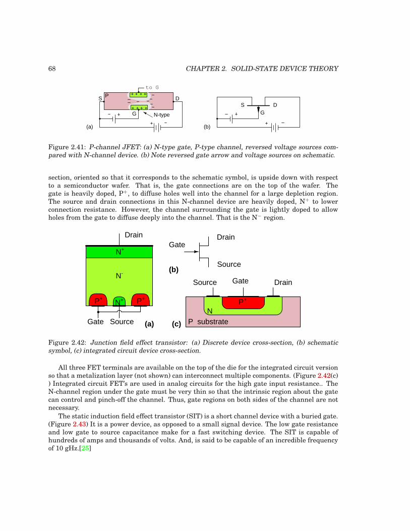
68 CHAPTER 2. SOLID-STATE DEVICE THEORY
GS D
(a) (b)
G
S D
N-type
P
to G
Figure 2.41: P-channel JFET: (a) N-type gate, P-type channel, reversed voltage sources com-pared with N-channel device. (b) Note reversed gate arrow and voltage sources on schematic.
section, oriented so that it corresponds to the schematic symbol, is upside down with respectto a semiconductor wafer. That is, the gate connections are on the top of the wafer. Thegate is heavily doped, P+, to diffuse holes well into the channel for a large depletion region.The source and drain connections in this N-channel device are heavily doped, N+ to lowerconnection resistance. However, the channel surrounding the gate is lightly doped to allowholes from the gate to diffuse deeply into the channel. That is the N− region.
Gate
Drain
Source
P substrate
Source
Drain
Gate
NP+
(a)
(b)
(c)
N-
N+
Drain
P+ P+N+
Gate Source
Figure 2.42: Junction field effect transistor: (a) Discrete device cross-section, (b) schematicsymbol, (c) integrated circuit device cross-section.
All three FET terminals are available on the top of the die for the integrated circuit versionso that a metalization layer (not shown) can interconnect multiple components. (Figure 2.42(c)) Integrated circuit FET’s are used in analog circuits for the high gate input resistance.. TheN-channel region under the gate must be very thin so that the intrinsic region about the gatecan control and pinch-off the channel. Thus, gate regions on both sides of the channel are notnecessary.
The static induction field effect transistor (SIT) is a short channel device with a buried gate.(Figure 2.43) It is a power device, as opposed to a small signal device. The low gate resistanceand low gate to source capacitance make for a fast switching device. The SIT is capable ofhundreds of amps and thousands of volts. And, is said to be capable of an incredible frequencyof 10 gHz.[25]
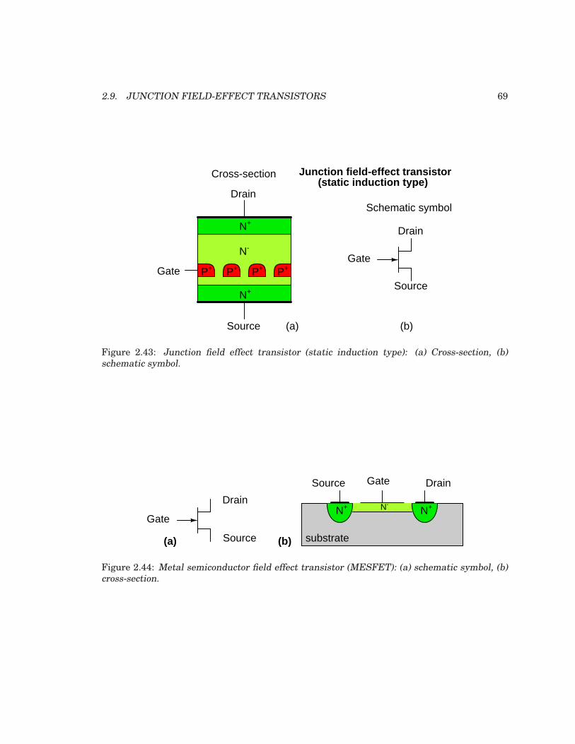
2.9. JUNCTION FIELD-EFFECT TRANSISTORS 69
Cross-section
Schematic symbol
Gate
Drain
Source
Junction field-effect transistor
Gate
(static induction type)
P+ P+ P+ P+
N-
N+
Drain
N+
Source (a) (b)
Figure 2.43: Junction field effect transistor (static induction type): (a) Cross-section, (b)schematic symbol.
Gate
Drain
Source substrate
Source
Drain
Gate
N-
(a) (b)
N+ N+
Figure 2.44: Metal semiconductor field effect transistor (MESFET): (a) schematic symbol, (b)cross-section.
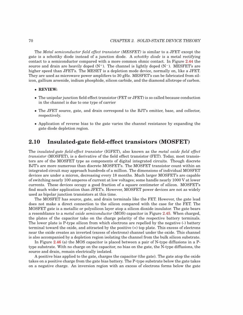
70 CHAPTER 2. SOLID-STATE DEVICE THEORY
The Metal semiconductor field effect transistor (MESFET) is similar to a JFET except thegate is a schottky diode instead of a junction diode. A schottky diode is a metal rectifyingcontact to a semiconductor compared with a more common ohmic contact. In Figure 2.44 thesource and drain are heavily doped (N+). The channel is lightly doped (N−). MESFET’s arehigher speed than JFET’s. The MESET is a depletion mode device, normally on, like a JFET.They are used as microwave power amplifiers to 30 gHz. MESFET’s can be fabricated from sil-icon, gallium arsenide, indium phosphide, silicon carbide, and the diamond allotrope of carbon.
• REVIEW:
• The unipolar junction field effect transistor (FET or JFET) is so called because conductionin the channel is due to one type of carrier
• The JFET source, gate, and drain correspond to the BJT’s emitter, base, and collector,respectively.
• Application of reverse bias to the gate varies the channel resistance by expanding thegate diode depletion region.
2.10 Insulated-gate field-effect transistors (MOSFET)
The insulated-gate field-effect transistor (IGFET), also known as the metal oxide field effect
transistor (MOSFET), is a derivative of the field effect transistor (FET). Today, most transis-tors are of the MOSFET type as components of digital integrated circuits. Though discreteBJT’s are more numerous than discrete MOSFET’s. The MOSFET transistor count within anintegrated circuit may approach hundreds of a million. The dimensions of individual MOSFETdevices are under a micron, decreasing every 18 months. Much larger MOSFET’s are capableof switching nearly 100 amperes of current at low voltages; some handle nearly 1000 V at lowercurrents. These devices occupy a good fraction of a square centimeter of silicon. MOSFET’sfind much wider application than JFET’s. However, MOSFET power devices are not as widelyused as bipolar junction transistors at this time.
The MOSFET has source, gate, and drain terminals like the FET. However, the gate leaddoes not make a direct connection to the silicon compared with the case for the FET. TheMOSFET gate is a metallic or polysilicon layer atop a silicon dioxide insulator. The gate bearsa resemblance to a metal oxide semiconductor (MOS) capacitor in Figure 2.45. When charged,the plates of the capacitor take on the charge polarity of the respective battery terminals.The lower plate is P-type silicon from which electrons are repelled by the negative (-) batteryterminal toward the oxide, and attracted by the positive (+) top plate. This excess of electronsnear the oxide creates an inverted (excess of electrons) channel under the oxide. This channelis also accompanied by a depletion region isolating the channel from the bulk silicon substrate.
In Figure 2.46 (a) the MOS capacitor is placed between a pair of N-type diffusions in a P-type substrate. With no charge on the capacitor, no bias on the gate, the N-type diffusions, thesource and drain, remain electrically isolated.
A positive bias applied to the gate, charges the capacitor (the gate). The gate atop the oxidetakes on a positive charge from the gate bias battery. The P-type substrate below the gate takeson a negative charge. An inversion region with an excess of electrons forms below the gate
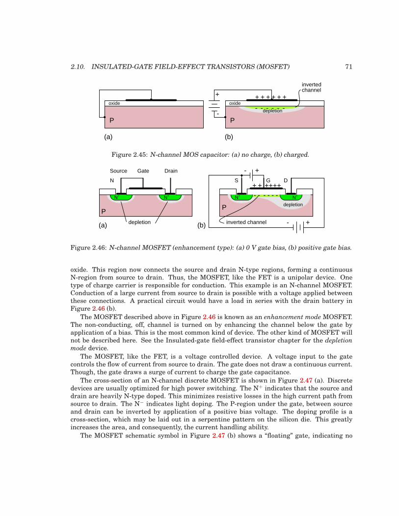
2.10. INSULATED-GATE FIELD-EFFECT TRANSISTORS (MOSFET) 71
P
+ + + + + ++
-- - - - - -depletion
oxide
inverted channel
P
oxide
(a) (b)
Figure 2.45: N-channel MOS capacitor: (a) no charge, (b) charged.
PP
Source Gate Drain
+-
- +S DG
(a) (b)
N+
+ + + ++--- - - -
+
inverted channel
depletion
depletion
Ν
N+N+ N+N+
Figure 2.46: N-channel MOSFET (enhancement type): (a) 0 V gate bias, (b) positive gate bias.
oxide. This region now connects the source and drain N-type regions, forming a continuousN-region from source to drain. Thus, the MOSFET, like the FET is a unipolar device. Onetype of charge carrier is responsible for conduction. This example is an N-channel MOSFET.Conduction of a large current from source to drain is possible with a voltage applied betweenthese connections. A practical circuit would have a load in series with the drain battery inFigure 2.46 (b).
The MOSFET described above in Figure 2.46 is known as an enhancement mode MOSFET.The non-conducting, off, channel is turned on by enhancing the channel below the gate byapplication of a bias. This is the most common kind of device. The other kind of MOSFET willnot be described here. See the Insulated-gate field-effect transistor chapter for the depletion
mode device.
The MOSFET, like the FET, is a voltage controlled device. A voltage input to the gatecontrols the flow of current from source to drain. The gate does not draw a continuous current.Though, the gate draws a surge of current to charge the gate capacitance.
The cross-section of an N-channel discrete MOSFET is shown in Figure 2.47 (a). Discretedevices are usually optimized for high power switching. The N+ indicates that the source anddrain are heavily N-type doped. This minimizes resistive losses in the high current path fromsource to drain. The N− indicates light doping. The P-region under the gate, between sourceand drain can be inverted by application of a positive bias voltage. The doping profile is across-section, which may be laid out in a serpentine pattern on the silicon die. This greatlyincreases the area, and consequently, the current handling ability.
The MOSFET schematic symbol in Figure 2.47 (b) shows a “floating” gate, indicating no
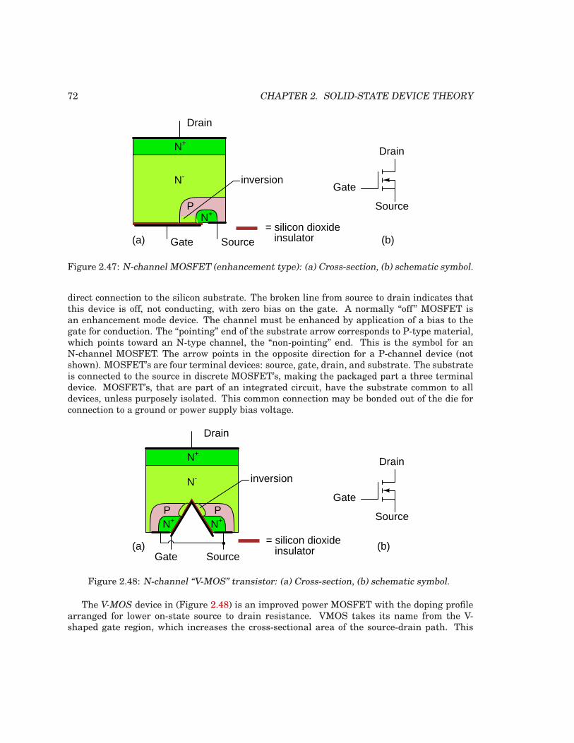
72 CHAPTER 2. SOLID-STATE DEVICE THEORY
Gate
Drain
Source
(b)= silicon dioxide insulator
N+
Drain
Gate(a) Source
N-
N+P
inversion
Figure 2.47: N-channel MOSFET (enhancement type): (a) Cross-section, (b) schematic symbol.
direct connection to the silicon substrate. The broken line from source to drain indicates thatthis device is off, not conducting, with zero bias on the gate. A normally “off” MOSFET isan enhancement mode device. The channel must be enhanced by application of a bias to thegate for conduction. The “pointing” end of the substrate arrow corresponds to P-type material,which points toward an N-type channel, the “non-pointing” end. This is the symbol for anN-channel MOSFET. The arrow points in the opposite direction for a P-channel device (notshown). MOSFET’s are four terminal devices: source, gate, drain, and substrate. The substrateis connected to the source in discrete MOSFET’s, making the packaged part a three terminaldevice. MOSFET’s, that are part of an integrated circuit, have the substrate common to alldevices, unless purposely isolated. This common connection may be bonded out of the die forconnection to a ground or power supply bias voltage.
Gate
Drain
Source
= silicon dioxide insulator (b)
N-
Drain
SourceGate
N+ N+P P
(a)
inversion
N+
Figure 2.48: N-channel “V-MOS” transistor: (a) Cross-section, (b) schematic symbol.
The V-MOS device in (Figure 2.48) is an improved power MOSFET with the doping profilearranged for lower on-state source to drain resistance. VMOS takes its name from the V-shaped gate region, which increases the cross-sectional area of the source-drain path. This
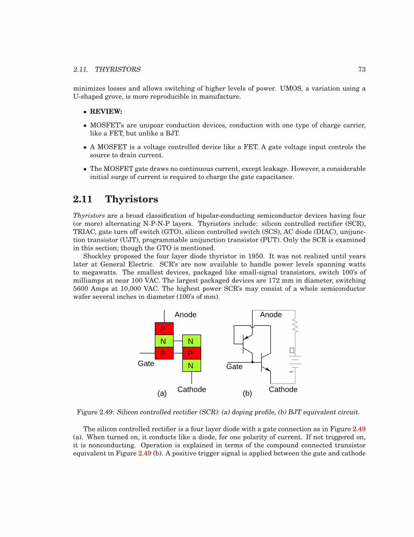
2.11. THYRISTORS 73
minimizes losses and allows switching of higher levels of power. UMOS, a variation using aU-shaped grove, is more reproducible in manufacture.
• REVIEW:
• MOSFET’s are unipoar conduction devices, conduction with one type of charge carrier,like a FET, but unlike a BJT.
• A MOSFET is a voltage controlled device like a FET. A gate voltage input controls thesource to drain current.
• The MOSFET gate draws no continuous current, except leakage. However, a considerableinitial surge of current is required to charge the gate capacitance.
2.11 Thyristors
Thyristors are a broad classification of bipolar-conducting semiconductor devices having four(or more) alternating N-P-N-P layers. Thyristors include: silicon controlled rectifier (SCR),TRIAC, gate turn off switch (GTO), silicon controlled switch (SCS), AC diode (DIAC), unijunc-tion transistor (UJT), programmable unijunction transistor (PUT). Only the SCR is examinedin this section; though the GTO is mentioned.
Shockley proposed the four layer diode thyristor in 1950. It was not realized until yearslater at General Electric. SCR’s are now available to handle power levels spanning wattsto megawatts. The smallest devices, packaged like small-signal transistors, switch 100’s ofmilliamps at near 100 VAC. The largest packaged devices are 172 mm in diameter, switching5600 Amps at 10,000 VAC. The highest power SCR’s may consist of a whole semiconductorwafer several inches in diameter (100’s of mm).
(a)
N
P
NN
P
P
Anode
Cathode
Gate Gate
Anode
Cathode
+
−
(b)
Figure 2.49: Silicon controlled rectifier (SCR): (a) doping profile, (b) BJT equivalent circuit.
The silicon controlled rectifier is a four layer diode with a gate connection as in Figure 2.49(a). When turned on, it conducts like a diode, for one polarity of current. If not triggered on,it is nonconducting. Operation is explained in terms of the compound connected transistorequivalent in Figure 2.49 (b). A positive trigger signal is applied between the gate and cathode
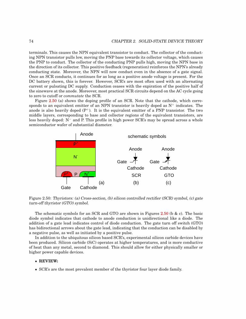
74 CHAPTER 2. SOLID-STATE DEVICE THEORY
terminals. This causes the NPN equivalent transistor to conduct. The collector of the conduct-ing NPN transistor pulls low, moving the PNP base towards its collector voltage, which causesthe PNP to conduct. The collector of the conducting PNP pulls high, moving the NPN base inthe direction of its collector. This positive feedback (regeneration) reinforces the NPN’s alreadyconducting state. Moreover, the NPN will now conduct even in the absence of a gate signal.Once an SCR conducts, it continues for as long as a positive anode voltage is present. For theDC battery shown, this is forever. However, SCR’s are most often used with an alternatingcurrent or pulsating DC supply. Conduction ceases with the expiration of the positive half ofthe sinewave at the anode. Moreover, most practical SCR circuits depend on the AC cycle goingto zero to cutoff or commutate the SCR.
Figure 2.50 (a) shows the doping profile of an SCR. Note that the cathode, which corre-sponds to an equivalent emitter of an NPN transistor is heavily doped as N+ indicates. Theanode is also heavily doped (P+). It is the equivalent emitter of a PNP transistor. The twomiddle layers, corresponding to base and collector regions of the equivalent transistors, areless heavily doped: N− and P. This profile in high power SCR’s may be spread across a wholesemiconductor wafer of substantial diameter.
Gate
Anode
Cathode
schematic symbols
Anode
GateCathode
(b) (c)
SCR GTO
(a)
N+P+
N-
P+
Anode
Gate Cathode
P
Figure 2.50: Thyristors: (a) Cross-section, (b) silicon controlled rectifier (SCR) symbol, (c) gateturn-off thyristor (GTO) symbol.
The schematic symbols for an SCR and GTO are shown in Figures 2.50 (b & c). The basicdiode symbol indicates that cathode to anode conduction is unidirectional like a diode. Theaddition of a gate lead indicates control of diode conduction. The gate turn off switch (GTO)has bidirectional arrows about the gate lead, indicating that the conduction can be disabled bya negative pulse, as well as initiated by a positive pulse.
In addition to the ubiquitous silicon based SCR’s, experimental silicon carbide devices havebeen produced. Silicon carbide (SiC) operates at higher temperatures, and is more conductiveof heat than any metal, second to diamond. This should allow for either physically smaller orhigher power capable devices.
• REVIEW:
• SCR’s are the most prevalent member of the thyristor four layer diode family.
2.12. SEMICONDUCTOR MANUFACTURING TECHNIQUES 75
• A positive pulse applied to the gate of an SCR triggers it into conduction. Conductioncontinues even if the gate pulse is removed. Conduction only ceases when the anode tocathode voltage drops to zero.
• SCR’s are most often used with an AC supply (or pulsating DC) because of the continuousconduction.
• A gate turn off switch (GTO) may be turned off by application of a negative pulse to thegate.
• SCR’s switch megawatts of power, up to 5600 A and 10,000 V.
2.12 Semiconductor manufacturing techniques
The manufacture of only silicon based semiconductors is described in this section; most semi-conductors are silicon. Silicon is particularly suitable for integrated circuits because it readilyforms an oxide coating, useful in patterning integrated components like transistors.
Silicon is the second most common element in the Earth’s crust in the form of silicon dioxide,SiO2, otherwise known as silica sand. Silicon is freed from silicon dioxide by reduction withcarbon in an electric arc furnace
SiO 2 + C = CO2+ SiSuch metalurgical grade silicon is suitable for use in silicon steel transformer laminations,
but not nearly pure enough for semiconductor applications. Conversion to the chloride SiCl4(or SiHCl3) allows purification by fractional distillation. Reduction by ultrapure zinc or mag-nesium yields sponge silicon, requiring further purification. Or, thermal decomposition on ahot polycrystalline silicon rod heater by hydrogen yields ultra pure silicon.
Si + 3HCl = SiHCl 3 + H2
SiHCl 3 + H2 = Si + 3HCl 2
The polycrystalline silicon is melted in a fused silica crucible heated by an induction heatedgraphite suceptor. The graphite heater may alternately be directly driven by a low voltageat high current. In the Czochralski process, the silicon melt is solidified on to a pencil sizedmonocrystal silicon rod of the desired crystal lattice orientation. (Figure 2.51) The rod is ro-tated and pulled upward at a rate to encourage the diameter to expand to several inches. Oncethis diameter is attained, the boule is automatically pulled at a rate to maintain a constantdiameter to a length of a few feet. Dopants may be added to the crucible melt to create, forexample, a P-type semiconductor. The growing apparatus is enclosed within an inert atmo-sphere.
The finished boule is ground to a precise final diameter, and the ends trimmed. The bouleis sliced into wafers by an inside diameter diamond saw. The wafers are ground flat andpolished. The wafers could have an N-type epitaxial layer grown atop the wafer by thermaldeposition for higher quality. Wafers at this stage of manufacture are delivered by the siliconwafer manufacturer to the semiconductor manufacturer.
The processing of semiconductors involves photo lithography, a process for making metallithographic printing plates by acid etching. The electronics based version of this is the pro-cessing of copper printed circuit boards. This is reviewed in Figure 2.53 as an easy introductionto the photo lithography involved in semiconductor processing.
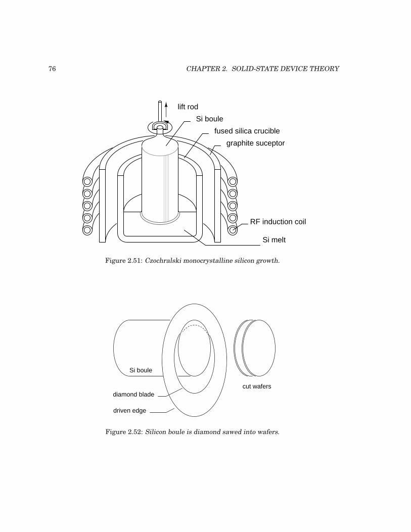
76 CHAPTER 2. SOLID-STATE DEVICE THEORY
fused silica crucible
Si boule
lift rod
graphite suceptor
RF induction coil
Si melt
Figure 2.51: Czochralski monocrystalline silicon growth.
Si boule
diamond blade
driven edge
cut wafers
Figure 2.52: Silicon boule is diamond sawed into wafers.
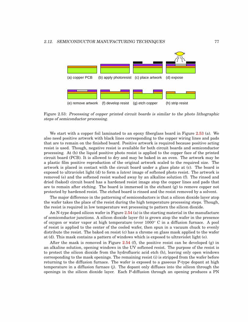
2.12. SEMICONDUCTOR MANUFACTURING TECHNIQUES 77
(a) copper PCB (b) apply photoresist (c) place artwork (d) expose
(e) remove artwork (f) develop resist (g) etch copper (h) strip resist
Figure 2.53: Processing of copper printed circuit boards is similar to the photo lithographicsteps of semiconductor processing.
We start with a copper foil laminated to an epoxy fiberglass board in Figure 2.53 (a). Wealso need positive artwork with black lines corresponding to the copper wiring lines and padsthat are to remain on the finished board. Positive artwork is required because positive actingresist is used. Though, negative resist is available for both circuit boards and semiconductorprocessing. At (b) the liquid positive photo resist is applied to the copper face of the printedcircuit board (PCB). It is allowed to dry and may be baked in an oven. The artwork may bea plastic film positive reproduction of the original artwork scaled to the required size. Theartwork is placed in contact with the circuit board under a glass plate at (c). The board isexposed to ultraviolet light (d) to form a latent image of softened photo resist. The artwork isremoved (e) and the softened resist washed away by an alkaline solution (f). The rinsed anddried (baked) circuit board has a hardened resist image atop the copper lines and pads thatare to remain after etching. The board is immersed in the etchant (g) to remove copper notprotected by hardened resist. The etched board is rinsed and the resist removed by a solvent.
The major difference in the patterning of semiconductors is that a silicon dioxide layer atopthe wafer takes the place of the resist during the high temperature processing steps. Though,the resist is required in low temperature wet processing to pattern the silicon dioxide.
An N-type doped silicon wafer in Figure 2.54 (a) is the starting material in the manufactureof semiconductor junctions. A silicon dioxide layer (b) is grown atop the wafer in the presenceof oxygen or water vapor at high temperature (over 1000o C in a diffusion furnace. A poolof resist is applied to the center of the cooled wafer, then spun in a vacuum chuck to evenlydistribute the resist. The baked on resist (c) has a chrome on glass mask applied to the waferat (d). This mask contains a pattern of windows which is exposed to ultraviolet light (e).
After the mask is removed in Figure 2.54 (f), the positive resist can be developed (g) inan alkaline solution, opening windows in the UV softened resist. The purpose of the resist isto protect the silicon dioxide from the hydrofluoric acid etch (h), leaving only open windowscorresponding to the mask openings. The remaining resist (i) is stripped from the wafer beforereturning to the diffusion furnace. The wafer is exposed to a gaseous P-type dopant at hightemperature in a diffusion furnace (j). The dopant only diffuses into the silicon through theopenings in the silicon dioxide layer. Each P-diffusion through an opening produces a PN
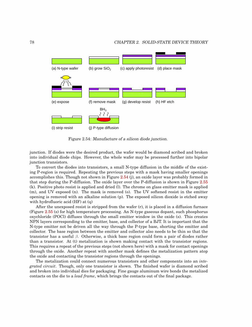
78 CHAPTER 2. SOLID-STATE DEVICE THEORY
(a) N-type wafer (b) grow SiO2 (c) apply photoresist (d) place mask
(e) expose (f) remove mask (g) develop resist (h) HF etch
BH3
(j) P-type diffusion(i) strip resist
Figure 2.54: Manufacture of a silicon diode junction.
junction. If diodes were the desired product, the wafer would be diamond scribed and brokeninto individual diode chips. However, the whole wafer may be processed further into bipolarjunction transistors.
To convert the diodes into transistors, a small N-type diffusion in the middle of the exist-ing P-region is required. Repeating the previous steps with a mask having smaller openingsaccomplishes this. Though not shown in Figure 2.54 (j), an oxide layer was probably formed inthat step during the P-diffusion. The oxide layer over the P-diffusion is shown in Figure 2.55(k). Positive photo resist is applied and dried (l). The chrome on glass emitter mask is applied(m), and UV exposed (n). The mask is removed (o). The UV softened resist in the emitteropening is removed with an alkaline solution (p). The exposed silicon dioxide is etched awaywith hydrofluoric acid (HF) at (q)
After the unexposed resist is stripped from the wafer (r), it is placed in a diffusion furnace(Figure 2.55 (s) for high temperature processing. An N-type gaseous dopant, such phosphorusoxychloride (POCl) diffuses through the small emitter window in the oxide (s). This createsNPN layers corresponding to the emitter, base, and collector of a BJT. It is important that theN-type emitter not be driven all the way through the P-type base, shorting the emitter andcollector. The base region between the emitter and collector also needs to be thin so that thetransistor has a useful β. Otherwise, a thick base region could form a pair of diodes ratherthan a transistor. At (t) metalization is shown making contact with the transistor regions.This requires a repeat of the previous steps (not shown here) with a mask for contact openingsthrough the oxide. Another repeat with another mask defines the metalization pattern atopthe oxide and contacting the transistor regions through the openings.
The metalization could connect numerous transistors and other components into an inte-
grated circuit. Though, only one transistor is shown. The finished wafer is diamond scribedand broken into individual dies for packaging. Fine gauge aluminum wire bonds the metalizedcontacts on the die to a lead frame, which brings the contacts out of the final package.
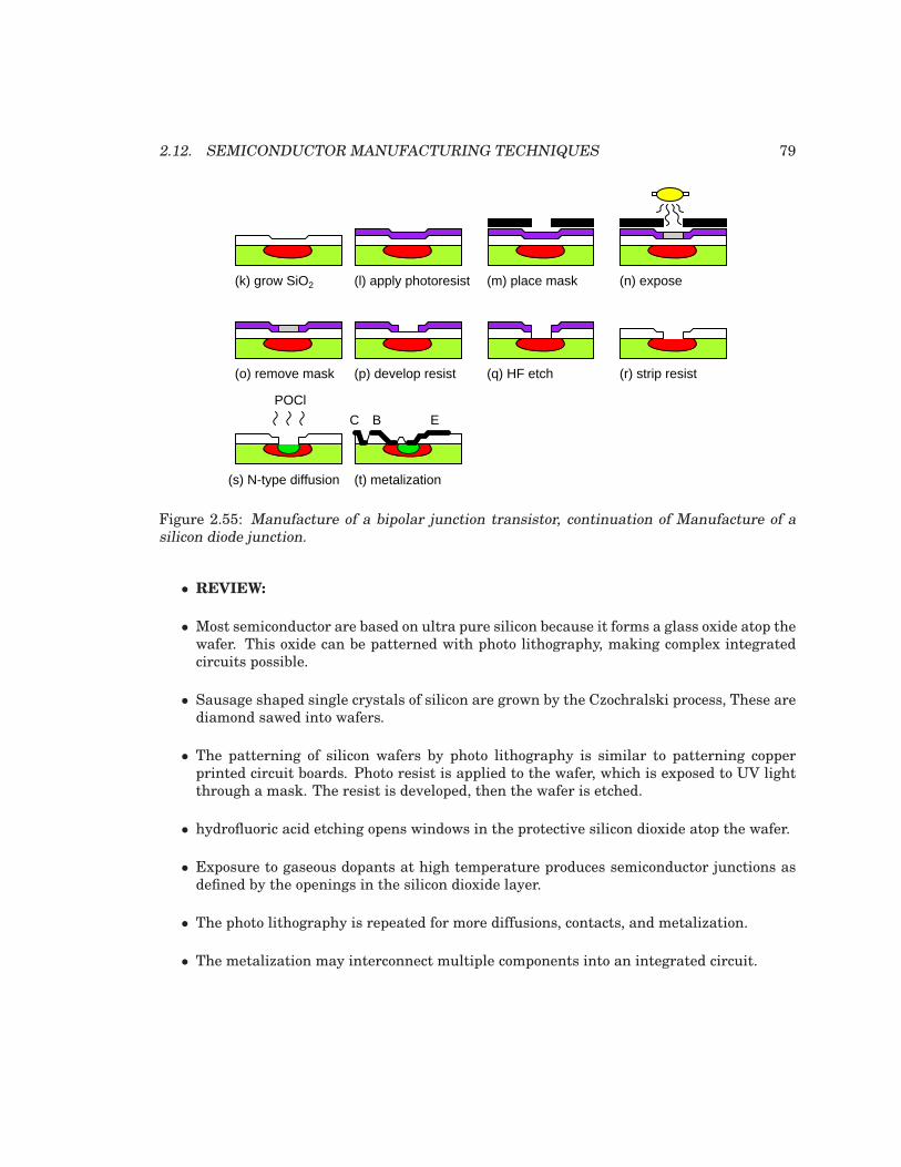
2.12. SEMICONDUCTOR MANUFACTURING TECHNIQUES 79
(k) grow SiO2 (l) apply photoresist (m) place mask (n) expose
(o) remove mask (q) HF etch
(s) N-type diffusion
POCl
(r) strip resist
C B E
(p) develop resist
(t) metalization
Figure 2.55: Manufacture of a bipolar junction transistor, continuation of Manufacture of asilicon diode junction.
• REVIEW:
• Most semiconductor are based on ultra pure silicon because it forms a glass oxide atop thewafer. This oxide can be patterned with photo lithography, making complex integratedcircuits possible.
• Sausage shaped single crystals of silicon are grown by the Czochralski process, These arediamond sawed into wafers.
• The patterning of silicon wafers by photo lithography is similar to patterning copperprinted circuit boards. Photo resist is applied to the wafer, which is exposed to UV lightthrough a mask. The resist is developed, then the wafer is etched.
• hydrofluoric acid etching opens windows in the protective silicon dioxide atop the wafer.
• Exposure to gaseous dopants at high temperature produces semiconductor junctions asdefined by the openings in the silicon dioxide layer.
• The photo lithography is repeated for more diffusions, contacts, and metalization.
• The metalization may interconnect multiple components into an integrated circuit.
80 CHAPTER 2. SOLID-STATE DEVICE THEORY
2.13 Superconducting devices
Superconducting devices, though not widely used, have some unique characteristics not avail-able in standard semiconductor devices. High sensitivity with respect to amplification of elec-trical signals, detection of magnetic fields, and detection of light are prized applications. Highspeed switching is also possible, though not applied to computers at this time. Conventionalsuperconducting devices must be cooled to within a few degrees of 0 Kelvin (-273 o C). Though,work is proceeding at this time on high temperature superconductor based devices, usable at 90K and below. This is significant because inexpensive liquid nitrogen may be used for cooling.
Superconductivity: Heike Onnes discovered superconductivity in mercury (Hg) in 1911,for which he won a Nobel prize. Most metals decrease electrical resistance with decreasingtemperature. Though, most do not decrease to zero resistance as 0 Kelvin is approached.Mercury is unique in that its resistance abruptly drops to zero Ω at 4.2 K. Superconductorslose all resistance abruptly when cooled below their critical temperature, Tc A property ofsuperconductivity is no power loss in conductors. Current may flow in a loop of superconductingwire for thousands of years. Super conductors include lead (Pb), aluminum, (Al), tin (Sn) andniobium (Nb).
Cooper pair: Lossless conduction in superconductors is not by ordinary electron flow. Elec-tron flow in normal conductors encounters opposition as collisions with the rigid ionic metalcrystal lattice. Decreasing vibrations of the crystal lattice with decreasing temperature ac-counts for decreasing resistance– up to a point. Lattice vibrations cease at absolute zero, butnot the energy dissipating collisions of electrons with the lattice. Thus, normal conductors donot lose all resistance at absolute zero.
Electrons in superconductors form a pair of electrons called a cooper pair, as temperaturedrops below the critical temperature at which superconductivity begins. The cooper pair existsbecause it is at a lower energy level than unpaired electrons. The electrons are attracted toeach other due to the exchange of phonons, very low energy particles related to vibrations. Thiscooper pair, quantum mechanical entity (particle or wave) is not subject to the normal lawsof physics. This entity propagates through the lattice without encountering the metal ionscomprising the fixed lattice. Thus, it dissipates no energy. The quantum mechanical natureof the cooper pair only allows it to exchange discrete amounts of energy, not continuouslyvariable amounts. An absolute minimum quantum of energy is acceptable to the cooper pair.If the vibrational energy of the crystal lattice is less, (due to the low temperature), the cooperpair cannot accept it, cannot be scattered by the lattice. Thus, under the critical temperature,the cooper pairs flow unimpeded through the lattice.
Josephson junctions: Brian Josephson won a Nobel prize for his 1962 prediction of theJosepheson junction. A Josephson junction is a pair of superconductors bridged by a thin insu-lator, as in Figure 2.56 (a), through which electrons can tunnel. The first Josephson junctionswere lead superconductors bridged by an insulator. These days a tri-layer of aluminum andniobium is preferred. Electrons can tunnel through the insulator even with zero voltage ap-plied across the superconductors.
If a voltage is applied across the junction, the current decreases and oscillates at a highfrequency proportional to voltage. The relationship between applied voltage and frequencyis so precise that the standard volt is now defined in terms of Josephson junction oscillationfrequency. The Josephson junction can also serve as a hyper-sensitive detector of low level mag-netic fields. It is also very sensitive to electromagnetic radiation from microwaves to gamma
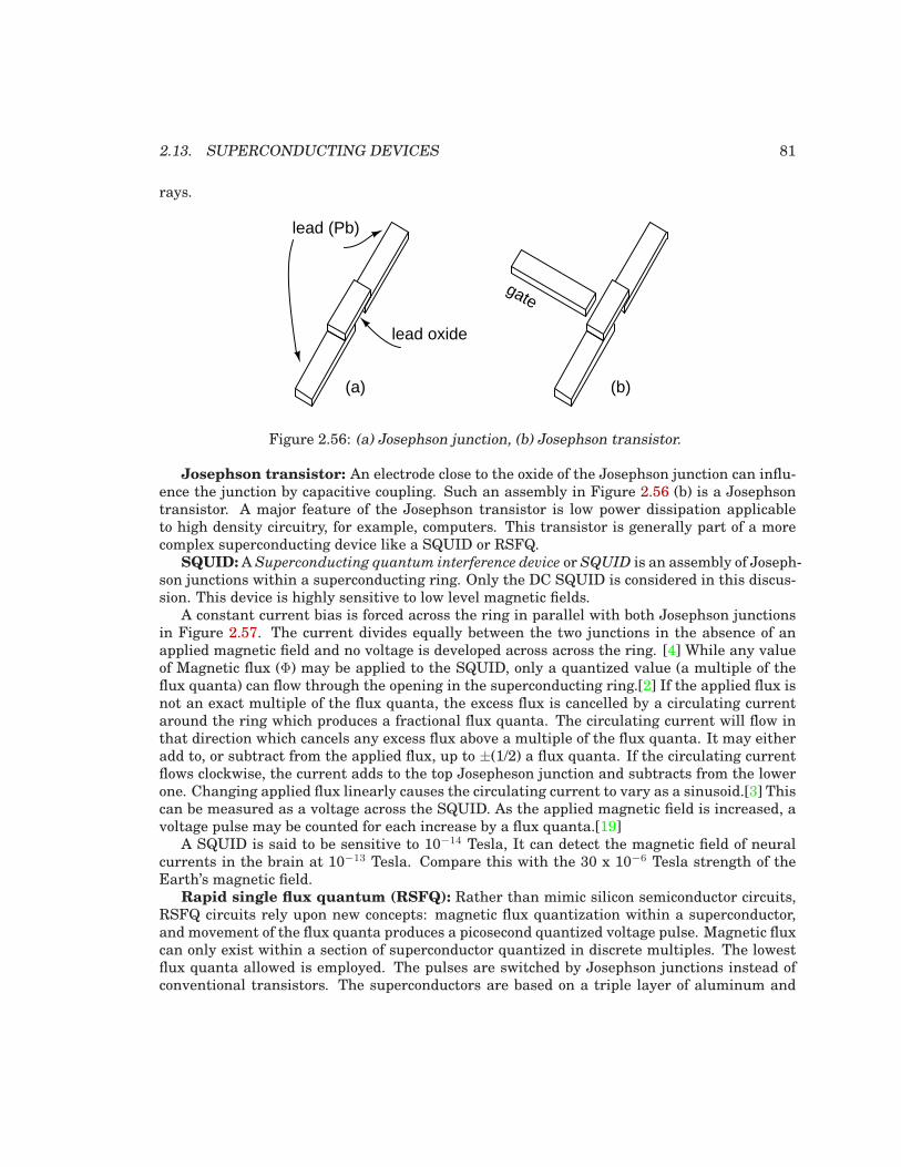
2.13. SUPERCONDUCTING DEVICES 81
rays.
lead (Pb)
lead oxide
gate
(a) (b)
Figure 2.56: (a) Josephson junction, (b) Josephson transistor.
Josephson transistor: An electrode close to the oxide of the Josephson junction can influ-ence the junction by capacitive coupling. Such an assembly in Figure 2.56 (b) is a Josephsontransistor. A major feature of the Josephson transistor is low power dissipation applicableto high density circuitry, for example, computers. This transistor is generally part of a morecomplex superconducting device like a SQUID or RSFQ.
SQUID:A Superconducting quantum interference device or SQUID is an assembly of Joseph-son junctions within a superconducting ring. Only the DC SQUID is considered in this discus-sion. This device is highly sensitive to low level magnetic fields.
A constant current bias is forced across the ring in parallel with both Josephson junctionsin Figure 2.57. The current divides equally between the two junctions in the absence of anapplied magnetic field and no voltage is developed across across the ring. [4] While any valueof Magnetic flux (Φ) may be applied to the SQUID, only a quantized value (a multiple of theflux quanta) can flow through the opening in the superconducting ring.[2] If the applied flux isnot an exact multiple of the flux quanta, the excess flux is cancelled by a circulating currentaround the ring which produces a fractional flux quanta. The circulating current will flow inthat direction which cancels any excess flux above a multiple of the flux quanta. It may eitheradd to, or subtract from the applied flux, up to ±(1/2) a flux quanta. If the circulating currentflows clockwise, the current adds to the top Josepheson junction and subtracts from the lowerone. Changing applied flux linearly causes the circulating current to vary as a sinusoid.[3] Thiscan be measured as a voltage across the SQUID. As the applied magnetic field is increased, avoltage pulse may be counted for each increase by a flux quanta.[19]
A SQUID is said to be sensitive to 10−14 Tesla, It can detect the magnetic field of neuralcurrents in the brain at 10−13 Tesla. Compare this with the 30 x 10−6 Tesla strength of theEarth’s magnetic field.
Rapid single flux quantum (RSFQ): Rather than mimic silicon semiconductor circuits,RSFQ circuits rely upon new concepts: magnetic flux quantization within a superconductor,and movement of the flux quanta produces a picosecond quantized voltage pulse. Magnetic fluxcan only exist within a section of superconductor quantized in discrete multiples. The lowestflux quanta allowed is employed. The pulses are switched by Josephson junctions instead ofconventional transistors. The superconductors are based on a triple layer of aluminum and
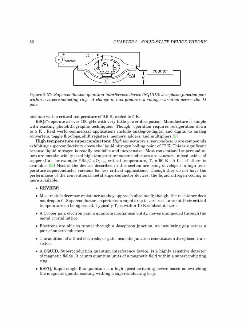
82 CHAPTER 2. SOLID-STATE DEVICE THEORY
JJ
+
-counter
ΦIconstant
JJ
±∆Ι V
Figure 2.57: Superconduction quantum interference device (SQUID): Josephson junction pairwithin a superconducting ring. A change in flux produces a voltage variation across the JJpair.
niobium with a critical temperature of 9.5 K, cooled to 5 K.RSQF’s operate at over 100 gHz with very little power dissipation. Manufacture is simple
with existing photolithographic techniques. Though, operation requires refrigeration downto 5 K . Real world commercial applications include analog-to-digital and digital to analogconverters, toggle flip-flops, shift registers, memory, adders, and multipliers.[5]
High temperature superconductors: High temperature superconductors are compoundsexhibiting superconductivity above the liquid nitrogen boiling point of 77 K. This is significantbecause liquid nitrogen is readily available and inexpensive. Most conventional superconduc-tors are metals; widely used high temperature superconductors are cuprates, mixed oxides ofcopper (Cu), for example YBa2Cu3O7−x, critical temperature, Tc = 90 K . A list of others isavailable.[23] Most of the devices described in this section are being developed in high tem-perature superconductor versions for less critical applications. Though they do not have theperformance of the conventional metal superconductor devices, the liquid nitrogen cooling ismore available.
• REVIEW:
• Most metals decrease resistance as they approach absolute 0; though, the resistance doesnot drop to 0. Superconductors experience a rapid drop to zero resistance at their criticaltemperature on being cooled. Typically Tc is within 10 K of absolute zero.
• A Cooper pair, electron pair, a quantum mechanical entity, moves unimpeded through themetal crystal lattice.
• Electrons are able to tunnel through a Josephson junction, an insulating gap across apair of superconductors.
• The addition of a third electrode, or gate, near the junction constitutes a Josephson tran-sistor.
• A SQUID, Superconduction quantum interference device, is a highly sensitive detectorof magnetic fields. It counts quantum units of a magnetic field within a superconductingring.
• RSFQ, Rapid single flux quantum is a high speed switching device based on switchingthe magnetic quanta existing withing a superconducting loop.
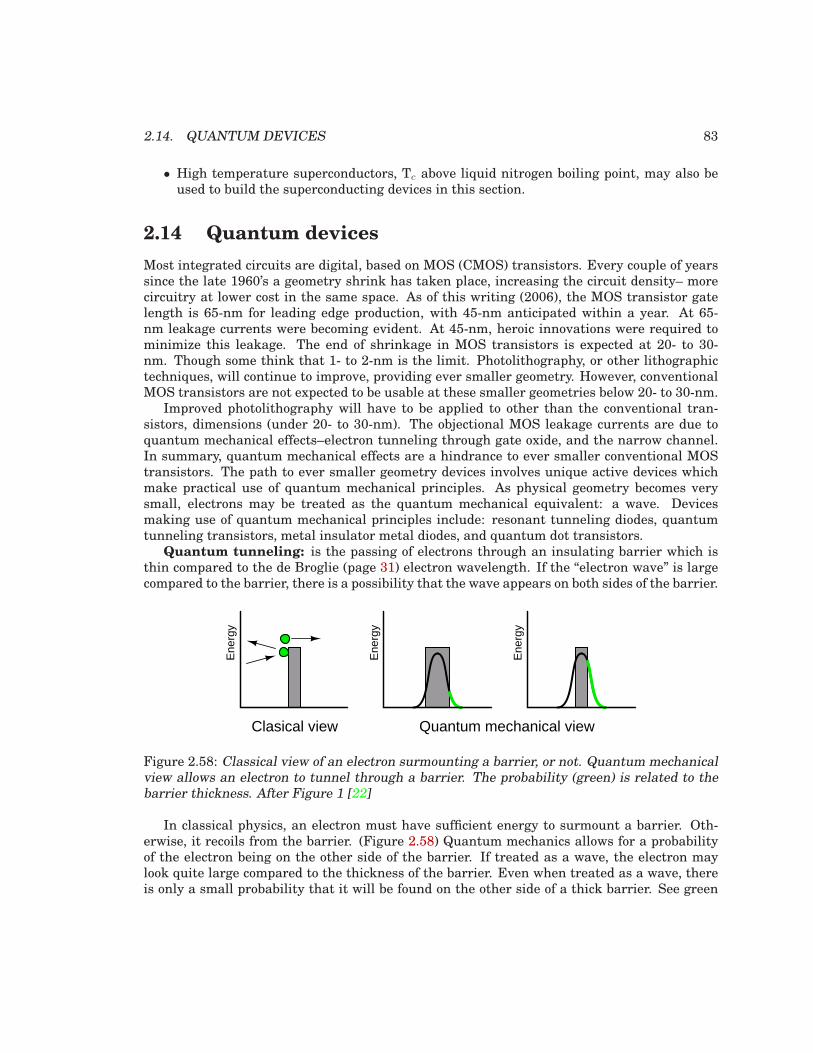
2.14. QUANTUM DEVICES 83
• High temperature superconductors, Tc above liquid nitrogen boiling point, may also beused to build the superconducting devices in this section.
2.14 Quantum devices
Most integrated circuits are digital, based on MOS (CMOS) transistors. Every couple of yearssince the late 1960’s a geometry shrink has taken place, increasing the circuit density– morecircuitry at lower cost in the same space. As of this writing (2006), the MOS transistor gatelength is 65-nm for leading edge production, with 45-nm anticipated within a year. At 65-nm leakage currents were becoming evident. At 45-nm, heroic innovations were required tominimize this leakage. The end of shrinkage in MOS transistors is expected at 20- to 30-nm. Though some think that 1- to 2-nm is the limit. Photolithography, or other lithographictechniques, will continue to improve, providing ever smaller geometry. However, conventionalMOS transistors are not expected to be usable at these smaller geometries below 20- to 30-nm.
Improved photolithography will have to be applied to other than the conventional tran-sistors, dimensions (under 20- to 30-nm). The objectional MOS leakage currents are due toquantum mechanical effects–electron tunneling through gate oxide, and the narrow channel.In summary, quantum mechanical effects are a hindrance to ever smaller conventional MOStransistors. The path to ever smaller geometry devices involves unique active devices whichmake practical use of quantum mechanical principles. As physical geometry becomes verysmall, electrons may be treated as the quantum mechanical equivalent: a wave. Devicesmaking use of quantum mechanical principles include: resonant tunneling diodes, quantumtunneling transistors, metal insulator metal diodes, and quantum dot transistors.
Quantum tunneling: is the passing of electrons through an insulating barrier which isthin compared to the de Broglie (page 31) electron wavelength. If the “electron wave” is largecompared to the barrier, there is a possibility that the wave appears on both sides of the barrier.
Clasical view Quantum mechanical view
Ene
rgy
Ene
rgy
Ene
rgy
Figure 2.58: Classical view of an electron surmounting a barrier, or not. Quantum mechanicalview allows an electron to tunnel through a barrier. The probability (green) is related to thebarrier thickness. After Figure 1 [22]
In classical physics, an electron must have sufficient energy to surmount a barrier. Oth-erwise, it recoils from the barrier. (Figure 2.58) Quantum mechanics allows for a probabilityof the electron being on the other side of the barrier. If treated as a wave, the electron maylook quite large compared to the thickness of the barrier. Even when treated as a wave, thereis only a small probability that it will be found on the other side of a thick barrier. See green
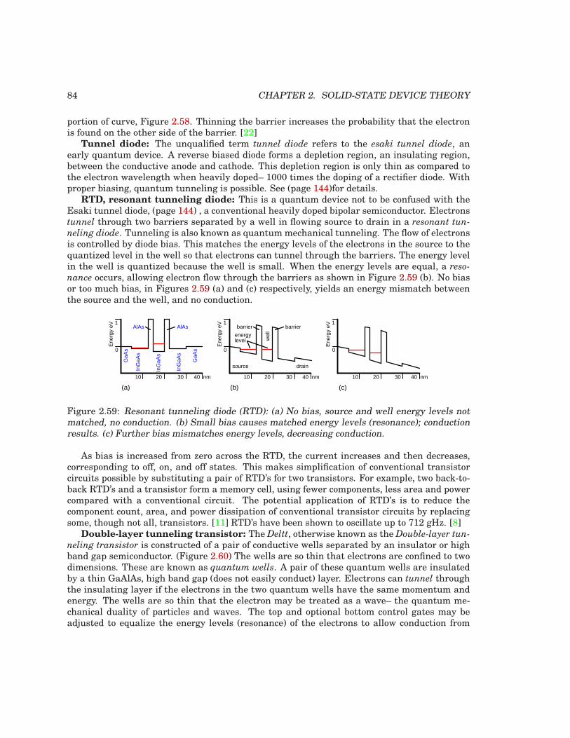
84 CHAPTER 2. SOLID-STATE DEVICE THEORY
portion of curve, Figure 2.58. Thinning the barrier increases the probability that the electronis found on the other side of the barrier. [22]
Tunnel diode: The unqualified term tunnel diode refers to the esaki tunnel diode, anearly quantum device. A reverse biased diode forms a depletion region, an insulating region,between the conductive anode and cathode. This depletion region is only thin as compared tothe electron wavelength when heavily doped– 1000 times the doping of a rectifier diode. Withproper biasing, quantum tunneling is possible. See (page 144)for details.
RTD, resonant tunneling diode: This is a quantum device not to be confused with theEsaki tunnel diode, (page 144) , a conventional heavily doped bipolar semiconductor. Electronstunnel through two barriers separated by a well in flowing source to drain in a resonant tun-
neling diode. Tunneling is also known as quantum mechanical tunneling. The flow of electronsis controlled by diode bias. This matches the energy levels of the electrons in the source to thequantized level in the well so that electrons can tunnel through the barriers. The energy levelin the well is quantized because the well is small. When the energy levels are equal, a reso-
nance occurs, allowing electron flow through the barriers as shown in Figure 2.59 (b). No biasor too much bias, in Figures 2.59 (a) and (c) respectively, yields an energy mismatch betweenthe source and the well, and no conduction.
GaA
s
InG
aAs
InG
aAs
InG
aAs
GaA
s
AlAs AlAs
10 20 30 40
Ene
rgy
eV
0
1
10 20 30 40
Ene
rgy
eV
0
1
10 20 30 40
Ene
rgy
eV
0
1
nm nmnm
(a) (b) (c)
wel
l
energylevel
drainsource
barrier barrier
Figure 2.59: Resonant tunneling diode (RTD): (a) No bias, source and well energy levels notmatched, no conduction. (b) Small bias causes matched energy levels (resonance); conductionresults. (c) Further bias mismatches energy levels, decreasing conduction.
As bias is increased from zero across the RTD, the current increases and then decreases,corresponding to off, on, and off states. This makes simplification of conventional transistorcircuits possible by substituting a pair of RTD’s for two transistors. For example, two back-to-back RTD’s and a transistor form a memory cell, using fewer components, less area and powercompared with a conventional circuit. The potential application of RTD’s is to reduce thecomponent count, area, and power dissipation of conventional transistor circuits by replacingsome, though not all, transistors. [11] RTD’s have been shown to oscillate up to 712 gHz. [8]
Double-layer tunneling transistor: The Deltt, otherwise known as the Double-layer tun-
neling transistor is constructed of a pair of conductive wells separated by an insulator or highband gap semiconductor. (Figure 2.60) The wells are so thin that electrons are confined to twodimensions. These are known as quantum wells. A pair of these quantum wells are insulatedby a thin GaAlAs, high band gap (does not easily conduct) layer. Electrons can tunnel throughthe insulating layer if the electrons in the two quantum wells have the same momentum andenergy. The wells are so thin that the electron may be treated as a wave– the quantum me-chanical duality of particles and waves. The top and optional bottom control gates may beadjusted to equalize the energy levels (resonance) of the electrons to allow conduction from
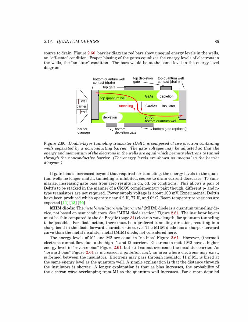
2.14. QUANTUM DEVICES 85
source to drain. Figure 2.60, barrier diagram red bars show unequal energy levels in the wells,an “off-state” condition. Proper biasing of the gates equalizes the energy levels of electrons inthe wells, the “on-state” condition. The bars would be at the same level in the energy leveldiagram.
GaAs
GaAs
GaAlAs
top depletion gate
top gate
bottom depletion gate
insulator
depletion
depletion
well
well
barrier
bottom gate (optional)
tunneling
top quantum well contact (drain)
bottom quantum well contact (drain)
bottom quantum well
top quantum well
barrier diagram
Figure 2.60: Double-layer tunneling transistor (Deltt) is composed of two electron containingwells separated by a nonconducting barrier. The gate voltages may be adjusted so that theenergy and momentum of the electrons in the wells are equal which permits electrons to tunnelthrough the nonconductive barrier. (The energy levels are shown as unequal in the barrierdiagram.)
If gate bias is increased beyond that required for tunneling, the energy levels in the quan-tum wells no longer match, tunneling is inhibited, source to drain current decreases. To sum-marize, increasing gate bias from zero results in on, off, on conditions. This allows a pair ofDeltt’s to be stacked in the manner of a CMOS complementary pair; though, different p- and n-type transistors are not required. Power supply voltage is about 100 mV. Experimental Deltt’shave been produced which operate near 4.2 K, 77 K, and 0o C. Room temperature versions areexpected.[11] [13] [20]
MIIM diode: Themetal-insulator-insulator-metal (MIIM) diode is a quantum tunneling de-vice, not based on semiconductors. See “MIIM diode section” Figure 2.61. The insulator layersmust be thin compared to the de Broglie (page 31) electron wavelength, for quantum tunnelingto be possible. For diode action, there must be a prefered tunneling direction, resulting in asharp bend in the diode forward characteristic curve. The MIIM diode has a sharper forwardcurve than the metal insulator metal (MIM) diode, not considered here.
The energy levels of M1 and M2 are equal in “no bias” Figure 2.61. However, (thermal)electrons cannot flow due to the high I1 and I2 barriers. Electrons in metal M2 have a higherenergy level in “reverse bias” Figure 2.61, but still cannot overcome the insulator barrier. As“forward bias” Figure 2.61 is increased, a quantum well, an area where electrons may exist,is formed between the insulators. Electrons may pass through insulator I1 if M1 is bised atthe same energy level as the quantum well. A simple explanation is that the distance throughthe insulators is shorter. A longer explanation is that as bias increases, the probability ofthe electron wave overlapping from M1 to the quantum well increases. For a more detailed
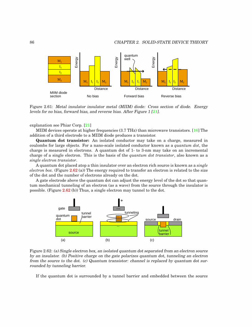
86 CHAPTER 2. SOLID-STATE DEVICE THEORY
Ene
rgy
Distance
M1
M2
I1
I2
M1 M2I1 I2
Ene
rgy
Distance
M1 M2
Ene
rgy
Distance
M1 M2 I1 I2I2 I1
MIIM diodesection No bias Forward bias Reverse bias
quantumwell
Figure 2.61: Metal insulator insulator metal (MIIM) diode: Cross section of diode. Energylevels for no bias, forward bias, and reverse bias. After Figure 1 [21].
explanation see Phiar Corp. [21]MIIM devices operate at higher frequencies (3.7 THz) than microwave transistors. [16] The
addition of a third electrode to a MIIM diode produces a transistor.Quantum dot transistor: An isolated conductor may take on a charge, measured in
coulombs for large objects. For a nano-scale isolated conductor known as a quantum dot, thecharge is measured in electrons. A quantum dot of 1- to 3-nm may take on an incrementalcharge of a single electron. This is the basis of the quantum dot transistor, also known as asingle electron transistor.
A quantum dot placed atop a thin insulator over an electron rich source is known as a single
electron box. (Figure 2.62 (a)) The energy required to transfer an electron is related to the sizeof the dot and the number of electrons already on the dot.
A gate electrode above the quantum dot can adjust the energy level of the dot so that quan-tum mechanical tunneling of an electron (as a wave) from the source through the insulator ispossible. (Figure 2.62 (b)) Thus, a single electron may tunnel to the dot.
source
gatetunnelbarrierquantum
dot
---
+++---
source drain
tunnel barrier
(a) (b) (c)
tunneling+++
+
Figure 2.62: (a) Single electron box, an isolated quantum dot separated from an electron sourceby an insulator. (b) Positive charge on the gate polarizes quantum dot, tunneling an electronfrom the source to the dot. (c) Quantum transistor: channel is replaced by quantum dot sur-rounded by tunneling barrier.
If the quantum dot is surrounded by a tunnel barrier and embedded between the source
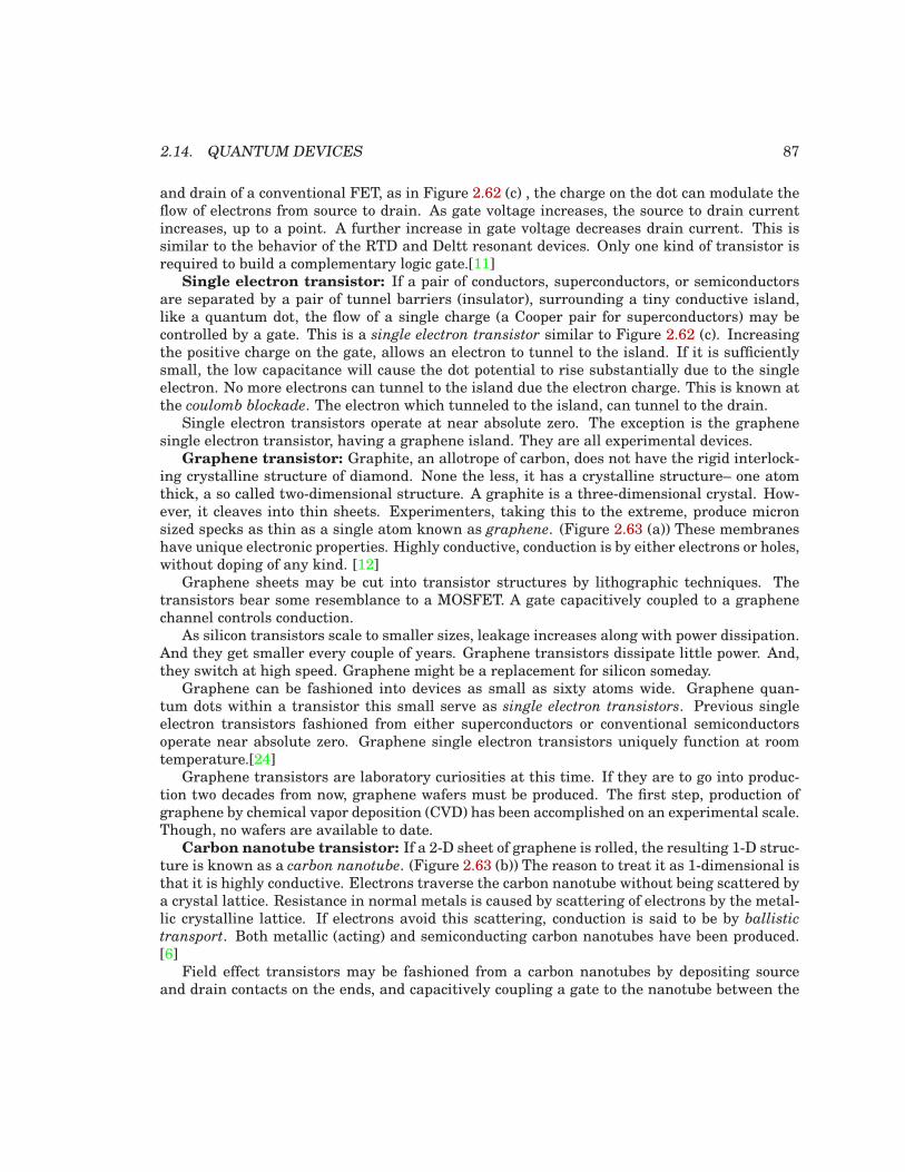
2.14. QUANTUM DEVICES 87
and drain of a conventional FET, as in Figure 2.62 (c) , the charge on the dot can modulate theflow of electrons from source to drain. As gate voltage increases, the source to drain currentincreases, up to a point. A further increase in gate voltage decreases drain current. This issimilar to the behavior of the RTD and Deltt resonant devices. Only one kind of transistor isrequired to build a complementary logic gate.[11]
Single electron transistor: If a pair of conductors, superconductors, or semiconductorsare separated by a pair of tunnel barriers (insulator), surrounding a tiny conductive island,like a quantum dot, the flow of a single charge (a Cooper pair for superconductors) may becontrolled by a gate. This is a single electron transistor similar to Figure 2.62 (c). Increasingthe positive charge on the gate, allows an electron to tunnel to the island. If it is sufficientlysmall, the low capacitance will cause the dot potential to rise substantially due to the singleelectron. No more electrons can tunnel to the island due the electron charge. This is known atthe coulomb blockade. The electron which tunneled to the island, can tunnel to the drain.
Single electron transistors operate at near absolute zero. The exception is the graphenesingle electron transistor, having a graphene island. They are all experimental devices.
Graphene transistor: Graphite, an allotrope of carbon, does not have the rigid interlock-ing crystalline structure of diamond. None the less, it has a crystalline structure– one atomthick, a so called two-dimensional structure. A graphite is a three-dimensional crystal. How-ever, it cleaves into thin sheets. Experimenters, taking this to the extreme, produce micronsized specks as thin as a single atom known as graphene. (Figure 2.63 (a)) These membraneshave unique electronic properties. Highly conductive, conduction is by either electrons or holes,without doping of any kind. [12]
Graphene sheets may be cut into transistor structures by lithographic techniques. Thetransistors bear some resemblance to a MOSFET. A gate capacitively coupled to a graphenechannel controls conduction.
As silicon transistors scale to smaller sizes, leakage increases along with power dissipation.And they get smaller every couple of years. Graphene transistors dissipate little power. And,they switch at high speed. Graphene might be a replacement for silicon someday.
Graphene can be fashioned into devices as small as sixty atoms wide. Graphene quan-tum dots within a transistor this small serve as single electron transistors. Previous singleelectron transistors fashioned from either superconductors or conventional semiconductorsoperate near absolute zero. Graphene single electron transistors uniquely function at roomtemperature.[24]
Graphene transistors are laboratory curiosities at this time. If they are to go into produc-tion two decades from now, graphene wafers must be produced. The first step, production ofgraphene by chemical vapor deposition (CVD) has been accomplished on an experimental scale.Though, no wafers are available to date.
Carbon nanotube transistor: If a 2-D sheet of graphene is rolled, the resulting 1-D struc-ture is known as a carbon nanotube. (Figure 2.63 (b)) The reason to treat it as 1-dimensional isthat it is highly conductive. Electrons traverse the carbon nanotube without being scattered bya crystal lattice. Resistance in normal metals is caused by scattering of electrons by the metal-lic crystalline lattice. If electrons avoid this scattering, conduction is said to be by ballistic
transport. Both metallic (acting) and semiconducting carbon nanotubes have been produced.[6]
Field effect transistors may be fashioned from a carbon nanotubes by depositing sourceand drain contacts on the ends, and capacitively coupling a gate to the nanotube between the
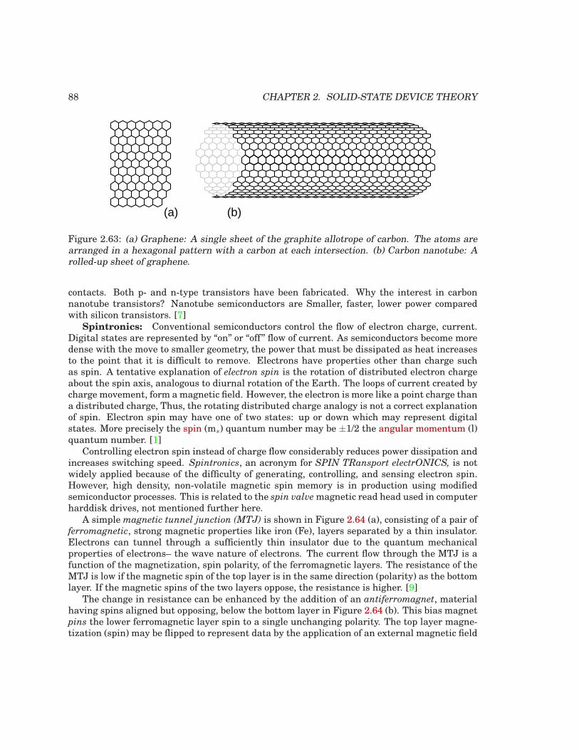
88 CHAPTER 2. SOLID-STATE DEVICE THEORY
(a) (b)
Figure 2.63: (a) Graphene: A single sheet of the graphite allotrope of carbon. The atoms arearranged in a hexagonal pattern with a carbon at each intersection. (b) Carbon nanotube: Arolled-up sheet of graphene.
contacts. Both p- and n-type transistors have been fabricated. Why the interest in carbonnanotube transistors? Nanotube semiconductors are Smaller, faster, lower power comparedwith silicon transistors. [7]
Spintronics: Conventional semiconductors control the flow of electron charge, current.Digital states are represented by “on” or “off” flow of current. As semiconductors become moredense with the move to smaller geometry, the power that must be dissipated as heat increasesto the point that it is difficult to remove. Electrons have properties other than charge suchas spin. A tentative explanation of electron spin is the rotation of distributed electron chargeabout the spin axis, analogous to diurnal rotation of the Earth. The loops of current created bycharge movement, form amagnetic field. However, the electron is more like a point charge thana distributed charge, Thus, the rotating distributed charge analogy is not a correct explanationof spin. Electron spin may have one of two states: up or down which may represent digitalstates. More precisely the spin (ms) quantum number may be ±1/2 the angular momentum (l)quantum number. [1]
Controlling electron spin instead of charge flow considerably reduces power dissipation andincreases switching speed. Spintronics, an acronym for SPIN TRansport electrONICS, is notwidely applied because of the difficulty of generating, controlling, and sensing electron spin.However, high density, non-volatile magnetic spin memory is in production using modifiedsemiconductor processes. This is related to the spin valvemagnetic read head used in computerharddisk drives, not mentioned further here.
A simple magnetic tunnel junction (MTJ) is shown in Figure 2.64 (a), consisting of a pair offerromagnetic, strong magnetic properties like iron (Fe), layers separated by a thin insulator.Electrons can tunnel through a sufficiently thin insulator due to the quantum mechanicalproperties of electrons– the wave nature of electrons. The current flow through the MTJ is afunction of the magnetization, spin polarity, of the ferromagnetic layers. The resistance of theMTJ is low if the magnetic spin of the top layer is in the same direction (polarity) as the bottomlayer. If the magnetic spins of the two layers oppose, the resistance is higher. [9]
The change in resistance can be enhanced by the addition of an antiferromagnet, materialhaving spins aligned but opposing, below the bottom layer in Figure 2.64 (b). This bias magnetpins the lower ferromagnetic layer spin to a single unchanging polarity. The top layer magne-tization (spin) may be flipped to represent data by the application of an external magnetic field
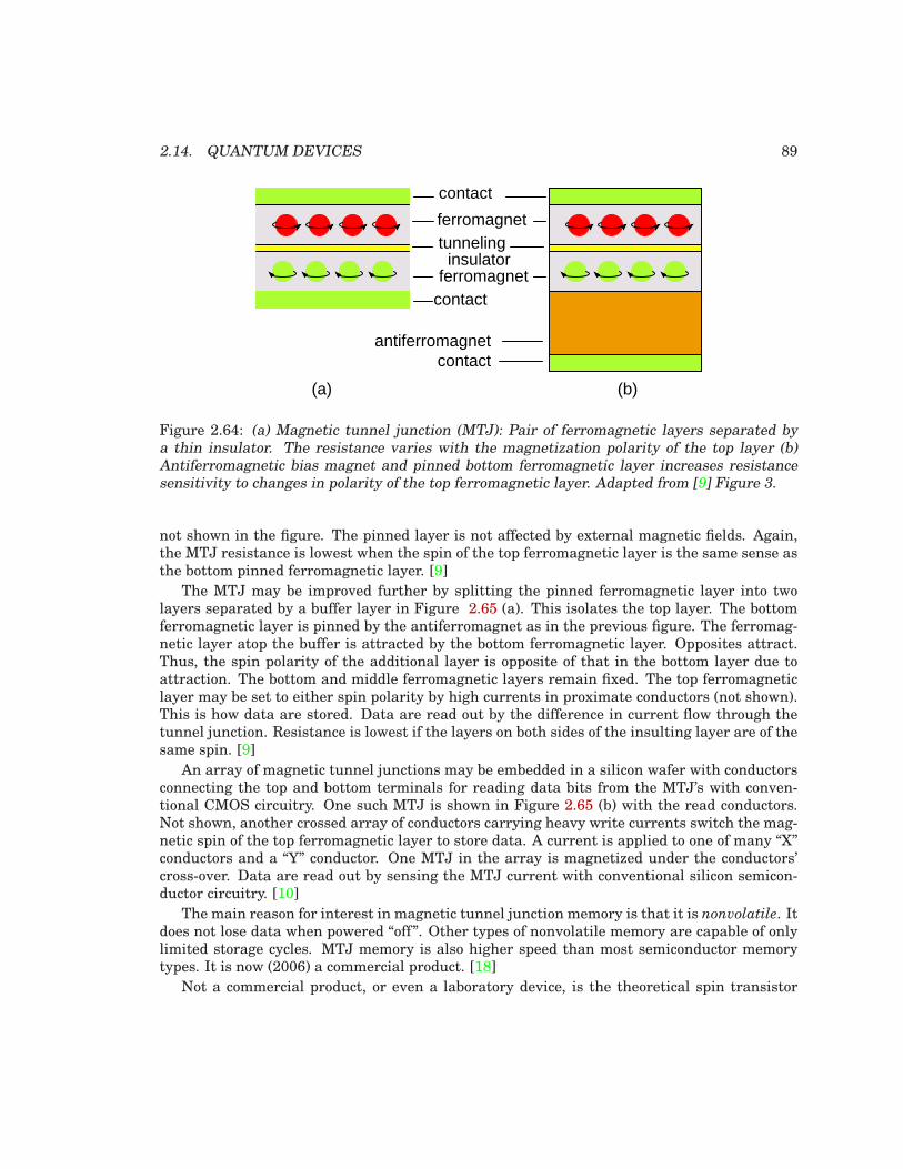
2.14. QUANTUM DEVICES 89
tunneling insulator
ferromagnet
contact
ferromagnet contact
antiferromagnet contact
(b)(a)
Figure 2.64: (a) Magnetic tunnel junction (MTJ): Pair of ferromagnetic layers separated bya thin insulator. The resistance varies with the magnetization polarity of the top layer (b)Antiferromagnetic bias magnet and pinned bottom ferromagnetic layer increases resistancesensitivity to changes in polarity of the top ferromagnetic layer. Adapted from [9] Figure 3.
not shown in the figure. The pinned layer is not affected by external magnetic fields. Again,the MTJ resistance is lowest when the spin of the top ferromagnetic layer is the same sense asthe bottom pinned ferromagnetic layer. [9]
The MTJ may be improved further by splitting the pinned ferromagnetic layer into twolayers separated by a buffer layer in Figure 2.65 (a). This isolates the top layer. The bottomferromagnetic layer is pinned by the antiferromagnet as in the previous figure. The ferromag-netic layer atop the buffer is attracted by the bottom ferromagnetic layer. Opposites attract.Thus, the spin polarity of the additional layer is opposite of that in the bottom layer due toattraction. The bottom and middle ferromagnetic layers remain fixed. The top ferromagneticlayer may be set to either spin polarity by high currents in proximate conductors (not shown).This is how data are stored. Data are read out by the difference in current flow through thetunnel junction. Resistance is lowest if the layers on both sides of the insulting layer are of thesame spin. [9]
An array of magnetic tunnel junctions may be embedded in a silicon wafer with conductorsconnecting the top and bottom terminals for reading data bits from the MTJ’s with conven-tional CMOS circuitry. One such MTJ is shown in Figure 2.65 (b) with the read conductors.Not shown, another crossed array of conductors carrying heavy write currents switch the mag-netic spin of the top ferromagnetic layer to store data. A current is applied to one of many “X”conductors and a “Y” conductor. One MTJ in the array is magnetized under the conductors’cross-over. Data are read out by sensing the MTJ current with conventional silicon semicon-ductor circuitry. [10]
The main reason for interest in magnetic tunnel junction memory is that it is nonvolatile. Itdoes not lose data when powered “off”. Other types of nonvolatile memory are capable of onlylimited storage cycles. MTJ memory is also higher speed than most semiconductor memorytypes. It is now (2006) a commercial product. [18]
Not a commercial product, or even a laboratory device, is the theoretical spin transistor
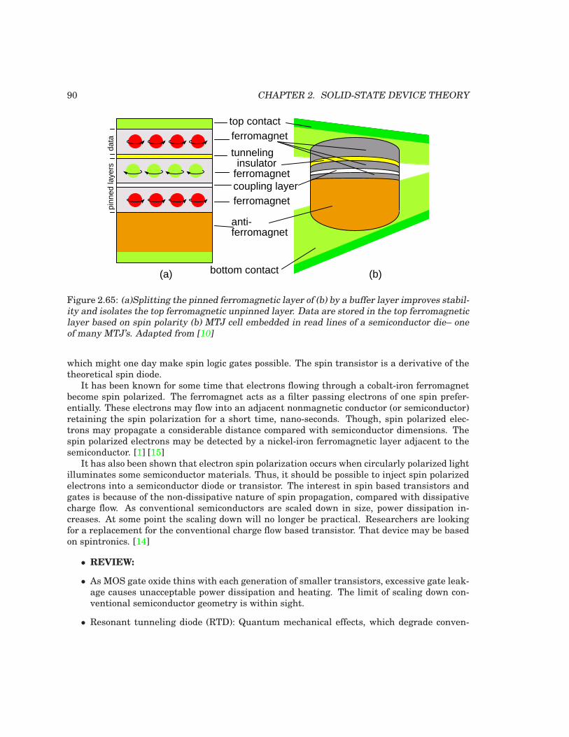
90 CHAPTER 2. SOLID-STATE DEVICE THEORY
tunneling insulator
coupling layer
anti-ferromagnet
ferromagnettop contact
bottom contact
ferromagnet
ferromagnet
(a) (b)
pinn
ed la
yers
data
Figure 2.65: (a)Splitting the pinned ferromagnetic layer of (b) by a buffer layer improves stabil-ity and isolates the top ferromagnetic unpinned layer. Data are stored in the top ferromagneticlayer based on spin polarity (b) MTJ cell embedded in read lines of a semiconductor die– oneof many MTJ’s. Adapted from [10]
which might one day make spin logic gates possible. The spin transistor is a derivative of thetheoretical spin diode.
It has been known for some time that electrons flowing through a cobalt-iron ferromagnetbecome spin polarized. The ferromagnet acts as a filter passing electrons of one spin prefer-entially. These electrons may flow into an adjacent nonmagnetic conductor (or semiconductor)retaining the spin polarization for a short time, nano-seconds. Though, spin polarized elec-trons may propagate a considerable distance compared with semiconductor dimensions. Thespin polarized electrons may be detected by a nickel-iron ferromagnetic layer adjacent to thesemiconductor. [1] [15]
It has also been shown that electron spin polarization occurs when circularly polarized lightilluminates some semiconductor materials. Thus, it should be possible to inject spin polarizedelectrons into a semiconductor diode or transistor. The interest in spin based transistors andgates is because of the non-dissipative nature of spin propagation, compared with dissipativecharge flow. As conventional semiconductors are scaled down in size, power dissipation in-creases. At some point the scaling down will no longer be practical. Researchers are lookingfor a replacement for the conventional charge flow based transistor. That device may be basedon spintronics. [14]
• REVIEW:
• As MOS gate oxide thins with each generation of smaller transistors, excessive gate leak-age causes unacceptable power dissipation and heating. The limit of scaling down con-ventional semiconductor geometry is within sight.
• Resonant tunneling diode (RTD): Quantum mechanical effects, which degrade conven-
2.15. SEMICONDUCTOR DEVICES IN SPICE 91
tional semiconductors, are employed in the RTD. The flow of electrons through a suffi-ciently thin insulator, is by the wave nature of the electron– particle wave duality. TheRTD functions as an amplifier.
• Double layer tunneling transistor (Deltt): The Deltt is a transistor version of the RTD.Gate bias controls the ability of electrons to tunnel through a thin insulator from onequantum well to another (source to drain).
• Quantum dot transistor: A quantum dot, capable of holding a charge, is surrounded by athin tunnel barrier replacing the gate of a conventional FET. The charge on the quantumdot controls source to drain current flow.
• Spintronics: Electrons have two basic properties: charge and spin. Conventional elec-tronic devices control the flow of charge, dissipating energy. Spintronic devices manipu-late electron spin, a propagative, non-dissipative process.
2.15 Semiconductor devices in SPICE
The SPICE (simulation program, integrated circuit emphesis) electronic simulation programprovides circuit elements and models for semiconductors. The SPICE element names beginwith d, q, j, or m correspond to diode, BJT, JFET and MOSFET elements, respectively. Theseelements are accompanied by corresponding “models” These models have extensive lists ofparameters describing the device. Though, we do not list them here. In this section we providea very brief listing of simple spice models for semiconductors, just enough to get started. Formore details on models and an extensive list of model parameters see Kuphaldt. [17] Thisreference also gives instructions on using SPICE.
Diode: The diode statement begins with a diode element name which must begin with “d”plus optional characters. Some example diode element names include: d1, d2, dtest, da, db,d101, etc. Two node numbers specify the connection of the anode and cathode, respectively, toother components. The node numbers are followed by a model name, referring to a “.model”statement.
The model statement line begins with “.model”, followed by the model name matching oneor more diode statements. Next is a “d” indicating that a diode is being modeled. The re-mainder of the model statement is a list of optional diode parameters of the form Parame-terName=ParameterValue. None are shown in the example below. For a list, see reference,“diodes”. [17]
General form: d[name] [anode] [cathode] [model].model [modelname] d ( [parmtr1=x] [parmtr2=y] . . .)
Example: d1 1 2 mod1.model mod1 d
Models for specific diode part numbers are often furnished by the semiconductor diode man-ufacturer. These models include parameters. Otherwise, the parameters default to so called“default values”, as in the example.
92 CHAPTER 2. SOLID-STATE DEVICE THEORY
BJT, bipolar junction transistor: The BJT element statement begins with an elementname which must begin with “q” with associated circuit symbol designator characters, exam-ple: q1, q2, qa, qgood. The BJT node numbers (connections) identify the wiring of the collector,base, emitter respectively. A model name following the node numbers is associated with amodel statement.
General form: q[name] [collector] [base] [emitter] [model ].model [modelname] [npn or pnp] ([parmtr1=x] . . .)
Example: q1 2 3 0 mod1.model mod1 pnp
Example: q2 7 8 9 q2n090.model q2n090 npn ( bf=75 )
The model statement begins with “.model”, followed by the model name, followed by oneof “npn” or “pnp”. The optional list of parameters follows, and may continue for a few linesbeginning with line continuation symbol “+”, plus. Shown above is the forward β parameterset to 75 for the hypothetical q2n090 model. Detailed transistor models are often availablefrom semiconductor manufacturers.
FET, field effect transistor The field effect transistor element statement begins with anelement name beginning with “j” for JFET associated with some unique characters, example:j101, j2b, jalpha, etc. The node numbers follow for the drain, gate and source terminals, re-spectively. The node numbers define connectivity to other circuit components. Finally, a modelname indicates the JFET model to use.
General form: j[name] [drain] [gate] [source] [model].model [modelname] [njf or pjf] ( [parmtr1=x] . . .)
Example: j1 2 3 0 mod1.model mod1 pjfj3 4 5 0 mod2.model mod2 njf ( vto=-4.0 )
The “.model” in the JFET model statement is followed by the model name to identify thismodel to the JFET element statement(s) using it. Following the model name is either pjf or njffor p-channel or n-channel JFET’s respectively. A long list of JFET parameters may follow. Weonly show how to set Vp, pinch off voltage, to -4.0 V for an n-channel JFET model. Otherwise,this vto parameter defaults to -2.5 V or 2.5V for n-channel or p-channel devices, respectively.
MOSFET, metal oxide field effect transistor The MOSFET element name must beginwith “m”, and is the first word in the element statement. Following are the four node numbersfor the drain, gate, source, and substrate, respectively. Next is the model name. Note that thesource and substrate are both connected to the same node “0” in the example. Discrete MOS-FET’s are packaged as three terminal devices, the source and substrate are the same physicalterminal. Integrated MOSFET’s are four terminal devices; the substrate is a fourth terminal.Integrated MOSFET’s may have numerous devices sharing the same substrate, separate fromthe sources. Though, the sources might still be connected to the common substrate.
General form: m[name] [drain] [gate] [source] [substrate] [model].model [modelname] [nmos or pmos] ( [parmtr1=x] . . . )

BIBLIOGRAPHY 93
Example: m1 2 3 0 0 mod1m5 5 6 0 0 mod4.model mod1 pmos.model mod4 nmos ( vto=1 )
The MOSFET model statement begins with “.model” followed by the model name followedby either “pmos” or “nmos”. Optional MOSFET model parameters follow. The list of possibleparameters is long. See Volume 5, “MOSFET” for details. [17] MOSFETmanufacturers providedetailed models. Otherwise, defaults are in effect.
The bare minimum semiconductor SPICE information is provided in this section. The mod-els shown here allow simulation of basic circuits. In particular, these models do not accountfor high speed or high frequency operation. Simulations are shown in the Volume 5 Chapter 7,“Using SPICE ...”.
• REVIEW:
• Semiconductors may be computer simulated with SPICE.
• SPICE provides element statements and models for the diode, BJT, JFET, and MOSFET.
Contributors
Contributors to this chapter are listed in chronological order of their contributions, from mostrecent to first. See Appendix 2 (Contributor List) for dates and contact information.
Maciej Noszczyski (December 2003): Corrected spelling of Niels Bohr’s name.Bill Heath (September 2002): Pointed out error in illustration of carbon atom – the nucleus
was shown with seven protons instead of six.
Bibliography
[1] David D. Awschalom, Michael E. Flatte, Nitin Samarth, “Spintronics”, Scientific Ameri-can, June 2002 at http://www.sciam.com
[2] John Bland, “The Fluxoid” in “A Mossbauer Spectroscopy and Mag-netometry Study of Magnetic Multilayers and Oxides”, Oliver LodgeLaboratory, Department of Physics, University of Liverpool, 2002, athttp://www.cmp.liv.ac.uk/frink/thesis/thesis/node45 .html
[3] John Bland, “Superconducting Quantum Interference Device (SQUID)” in “A Moss-bauer Spectroscopy and Magnetometry Study of Magnetic Multilayers and Oxides”,Oliver Lodge Laboratory, Department of Physics, University of Liverpool, 2002, athttp://www.cmp.liv.ac.uk/frink/thesis/thesis/node48 .html
[4] John Bland, “SQUID Magnetometer” in “A Mossbauer Spectroscopy andMagnetometry Study of Magnetic Multilayers and Oxides”, Oliver Lodge

94 CHAPTER 2. SOLID-STATE DEVICE THEORY
Laboratory, Department of Physics, University of Liverpool, 2002, athttp://www.cmp.liv.ac.uk/frink/thesis/thesis/node48 .html
[5] Darren K. Brock, “RSFQ Technology: Circuits and Systems”, Hypres, Inc., NY, athttp://www.hypres.com/papers/Brock-RSFQ-CirSys-Rev0 1.pdf
[6] Matthew Broersma , “Nanotubes break semiconducting record”, Cnet News, December19, 2003, at http://news.com.com/2100-1006-5129761.html
[7] “Carbon Nanotube Transistor”, Physics News Graphics, May 13, 1998, athttp://www.aip.org/mgr/png/html/tubefet.htm
[8] E. R. Brown, C. D. Parker, “Resonant Tunnel Diodes as Submillimetre-WaveSources”, Philosophical Transactions: Mathematical, Physical and Engineer-ing Sciences, Vol. 354, No. 1717, The Current Status of Semiconductor Tun-nelling Devices (Oct. 15, 1996), pp. 2365-2381 at http://links.jstor.org/sici?sici=1364-503X(19961015)354%3A1717%3C2365%3ART DASS%3E2.0.CO%3B2-Q
[9] W. J. Gallagher, S. S. P. Parkin, “Development of the magnetic tunnel junc-tion MRAM at IBM: From first junctions to a 16-Mb MRAM demonstrator chip”,IBM Research and Development, Spintronics, Volume 50, Number 1, 2006, athttp://www.research.ibm.com/journal/rd/501/gallaghe r.html
[10] “IBM, Infineon Develop Most Advanced MRAM Technology to Date”, IBM Research, athttp://domino.research.ibm.com/comm/pr.nsf/pages/ne ws.20030610 mram.html
[11] Linda Geppert “Quantum Transistors: toward nanoectronic”, IEEE Spectrum, September2000, at http://www.ece.osu.edu/˜berger/press/quan0900.pdf
[12] A. K. Geim1 and K. S. Novoselov1 , “The rise of graphene”, Nature Materials, 6, 2007, athttp://www.nature.com/nmat/journal/v6/n3/full/nmat1 849.html
[13] Ilan Greenberg, “Transistor Technology Takes a Quantum Leap”, Wired News, December8, 1997, at http://www.wired.com/news/technology/0,1282,8994,00 .html
[14] R. Colin Johnson, “Spintronics approach advances toward live chips,” EE Times,11/06/2006, at http://www.eetimes.com/showArticle.jhtml?articleID= 193500309
[15] R. Colin Johnson “ U. of Delaware researchers edge closer to spintronics,” EE Times,07/26/2007, at http://www.eetimes.com/news/design/showArticle.jhtm l?articleID=201201400
[16] R. Colin Johnson, “Can metal-insulator electronics do it better, sans semiconductors?”http://www.eetimes.com/showArticle.jhtml?articleID= 201200024
[17] Tony R. Kuphaldt, “Lessons in Electricity”, Reference, Vol. 5, Ch 7, 2007 athttp://www.ibiblio.org/obp/electricCircuits/Ref/spi ce.html
[18] Tom Lee, “Is nonvolatile MRAM right for your consumer em-bedded device application? ”, Freescale Semiconductor athttp://www.acumeninfo.com/subscriber/article/getArt icle.jhtml?articleId=197006965
BIBLIOGRAPHY 95
[19] HyperPhysics, “SQUID Magnetometer”, HyperPhysics athttp://hyperphysics.phy-astr.gsu.edu/hbase/solids/s quid.html
[20] Phillip F. Schewe, Ben Stein, “A Quantum Tunneling Transis-tor”, Physics Nessw Update, Number 357, February 4, 1998, athttp://www.aip.org/pnu/1998/physnews.357.htm
[21] “Why MIIM?”, Phiar Corporation, at http://www.phiar.com/whyMIIM.php4
[22] “What is Quantum Tunneling?”, Phiar Corporation, athttp://www.phiar.com/whatQuantum.php4
[23] Oxford University, “Theory, Superconductor Synthesis”, Oxford University, 1996, athttp://www.chem.ox.ac.uk/vrchemistry/super/theory.h tm
[24] John Walko, “Graphene transistor to rival silicon, say researchers”, EE Times Eu-rope, 03/02/2007, at http://www.eetimes.com/news/design/showArticle.jhtm l?articleID=197700700
[25] Ying-Yu Tzou,“Power Electronics: An Introduction”, Instituteof Control Engineering, National Chiao Tung University, athttp://pemclab.cn.nctu.edu.tw/peclub/w3cnotes

96 CHAPTER 2. SOLID-STATE DEVICE THEORY
Chapter 3
DIODES AND RECTIFIERS
Contents
3.1 Introduction . . . . . . . . . . . . . . . . . . . . . . . . . . . . . . . . . . . . . . 98
3.2 Meter check of a diode . . . . . . . . . . . . . . . . . . . . . . . . . . . . . . . 103
3.3 Diode ratings . . . . . . . . . . . . . . . . . . . . . . . . . . . . . . . . . . . . . 107
3.4 Rectifier circuits . . . . . . . . . . . . . . . . . . . . . . . . . . . . . . . . . . . 108
3.5 Peak detector . . . . . . . . . . . . . . . . . . . . . . . . . . . . . . . . . . . . . 115
3.6 Clipper circuits . . . . . . . . . . . . . . . . . . . . . . . . . . . . . . . . . . . . 117
3.7 Clamper circuits . . . . . . . . . . . . . . . . . . . . . . . . . . . . . . . . . . . 121
3.8 Voltage multipliers . . . . . . . . . . . . . . . . . . . . . . . . . . . . . . . . . . 123
3.9 Inductor commutating circuits . . . . . . . . . . . . . . . . . . . . . . . . . . 130
3.10 Diode switching circuits . . . . . . . . . . . . . . . . . . . . . . . . . . . . . . 132
3.10.1 Logic . . . . . . . . . . . . . . . . . . . . . . . . . . . . . . . . . . . . . . . 132
3.10.2 Analog switch . . . . . . . . . . . . . . . . . . . . . . . . . . . . . . . . . . 134
3.11 Zener diodes . . . . . . . . . . . . . . . . . . . . . . . . . . . . . . . . . . . . . . 135
3.12 Special-purpose diodes . . . . . . . . . . . . . . . . . . . . . . . . . . . . . . . 143
3.12.1 Schottky diodes . . . . . . . . . . . . . . . . . . . . . . . . . . . . . . . . . 143
3.12.2 Tunnel diodes . . . . . . . . . . . . . . . . . . . . . . . . . . . . . . . . . . 144
3.12.3 Light-emitting diodes . . . . . . . . . . . . . . . . . . . . . . . . . . . . . . 146
3.12.4 Laser diodes . . . . . . . . . . . . . . . . . . . . . . . . . . . . . . . . . . . 150
3.12.5 Photodiodes . . . . . . . . . . . . . . . . . . . . . . . . . . . . . . . . . . . 152
3.12.6 Solar cells . . . . . . . . . . . . . . . . . . . . . . . . . . . . . . . . . . . . 154
3.12.7 Varicap or varactor diodes . . . . . . . . . . . . . . . . . . . . . . . . . . . 158
3.12.8 Snap diode . . . . . . . . . . . . . . . . . . . . . . . . . . . . . . . . . . . . 159
3.12.9 PIN diodes . . . . . . . . . . . . . . . . . . . . . . . . . . . . . . . . . . . . 159
3.12.10 IMPATT diode . . . . . . . . . . . . . . . . . . . . . . . . . . . . . . . . . . 160
3.12.11Gunn diode . . . . . . . . . . . . . . . . . . . . . . . . . . . . . . . . . . . . 161
3.12.12Shockley diode . . . . . . . . . . . . . . . . . . . . . . . . . . . . . . . . . . 162
3.12.13Constant-current diodes . . . . . . . . . . . . . . . . . . . . . . . . . . . . 162
97
98 CHAPTER 3. DIODES AND RECTIFIERS
3.13 Other diode technologies . . . . . . . . . . . . . . . . . . . . . . . . . . . . . . 163
3.13.1 SiC diodes . . . . . . . . . . . . . . . . . . . . . . . . . . . . . . . . . . . . 163
3.13.2 Polymer diode . . . . . . . . . . . . . . . . . . . . . . . . . . . . . . . . . . 163
3.14 SPICE models . . . . . . . . . . . . . . . . . . . . . . . . . . . . . . . . . . . . . 163
Bibliography . . . . . . . . . . . . . . . . . . . . . . . . . . . . . . . . . . . . . . . . . 172
3.1 Introduction
A diode is an electrical device allowing current to move through it in one direction with fargreater ease than in the other. The most common kind of diode in modern circuit design isthe semiconductor diode, although other diode technologies exist. Semiconductor diodes aresymbolized in schematic diagrams such as Figure 3.1. The term “diode” is customarily reservedfor small signal devices, I ≤ 1 A. The term rectifier is used for power devices, I > 1 A.
Figure 3.1: Semiconductor diode schematic symbol: Arrows indicate the direction of electroncurrent flow.
When placed in a simple battery-lamp circuit, the diode will either allow or prevent currentthrough the lamp, depending on the polarity of the applied voltage. (Figure 3.2)
+
- +
-
(a) (b)
Figure 3.2: Diode operation: (a) Current flow is permitted; the diode is forward biased. (b)Current flow is prohibited; the diode is reversed biased.
When the polarity of the battery is such that electrons are allowed to flow through thediode, the diode is said to be forward-biased. Conversely, when the battery is “backward” andthe diode blocks current, the diode is said to be reverse-biased. A diode may be thought of aslike a switch: “closed” when forward-biased and “open” when reverse-biased.
Oddly enough, the direction of the diode symbol’s “arrowhead” points against the directionof electron flow. This is because the diode symbol was invented by engineers, who predomi-nantly use conventional flow notation in their schematics, showing current as a flow of chargefrom the positive (+) side of the voltage source to the negative (-). This convention holds truefor all semiconductor symbols possessing “arrowheads:” the arrow points in the permitted di-rection of conventional flow, and against the permitted direction of electron flow.
3.1. INTRODUCTION 99
Flow permitted Flow prohibited
Hydrauliccheck valve
-+ +-
(a) (b)
Figure 3.3: Hydraulic check valve analogy: (a) Electron current flow permitted. (b) Currentflow prohibited.
Diode behavior is analogous to the behavior of a hydraulic device called a check valve. Acheck valve allows fluid flow through it in only one direction as in Figure 3.3.
Check valves are essentially pressure-operated devices: they open and allow flow if thepressure across them is of the correct “polarity” to open the gate (in the analogy shown, greaterfluid pressure on the right than on the left). If the pressure is of the opposite “polarity,” thepressure difference across the check valve will close and hold the gate so that no flow occurs.
Like check valves, diodes are essentially “pressure-” operated (voltage-operated) devices.The essential difference between forward-bias and reverse-bias is the polarity of the voltagedropped across the diode. Let’s take a closer look at the simple battery-diode-lamp circuitshown earlier, this time investigating voltage drops across the various components in Fig-ure 3.4.
+
- +
-
6 V 6 V
+-
V Ω
COMA
0.7 V
-+
V Ω
COMA
5.3 V
V Ω
COMA
V Ω
COMA
6.0 V
0.0 V
(a) (b)
Figure 3.4: Diode circuit voltage measurements: (a) Forward biased. (b) Reverse biased.
A forward-biased diode conducts current and drops a small voltage across it, leaving mostof the battery voltage dropped across the lamp. If the battery’s polarity is reversed, the diodebecomes reverse-biased, and drops all of the battery’s voltage leaving none for the lamp. If weconsider the diode to be a self-actuating switch (closed in the forward-bias mode and open inthe reverse-bias mode), this behavior makes sense. The most substantial difference is that thediode drops a lot more voltage when conducting than the average mechanical switch (0.7 voltsversus tens of millivolts).
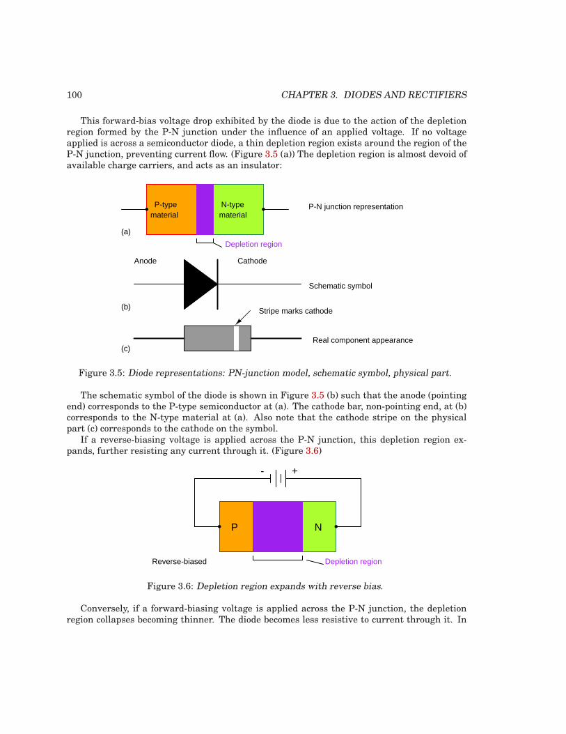
100 CHAPTER 3. DIODES AND RECTIFIERS
This forward-bias voltage drop exhibited by the diode is due to the action of the depletionregion formed by the P-N junction under the influence of an applied voltage. If no voltageapplied is across a semiconductor diode, a thin depletion region exists around the region of theP-N junction, preventing current flow. (Figure 3.5 (a)) The depletion region is almost devoid ofavailable charge carriers, and acts as an insulator:
Anode Cathode
Stripe marks cathode
P-N junction representation
Schematic symbol
Real component appearance
Depletion region
P-typematerial
N-typematerial
(a)
(b)
(c)
Figure 3.5: Diode representations: PN-junction model, schematic symbol, physical part.
The schematic symbol of the diode is shown in Figure 3.5 (b) such that the anode (pointingend) corresponds to the P-type semiconductor at (a). The cathode bar, non-pointing end, at (b)corresponds to the N-type material at (a). Also note that the cathode stripe on the physicalpart (c) corresponds to the cathode on the symbol.
If a reverse-biasing voltage is applied across the P-N junction, this depletion region ex-pands, further resisting any current through it. (Figure 3.6)
Reverse-biased Depletion region
P N
+-
Figure 3.6: Depletion region expands with reverse bias.
Conversely, if a forward-biasing voltage is applied across the P-N junction, the depletionregion collapses becoming thinner. The diode becomes less resistive to current through it. In
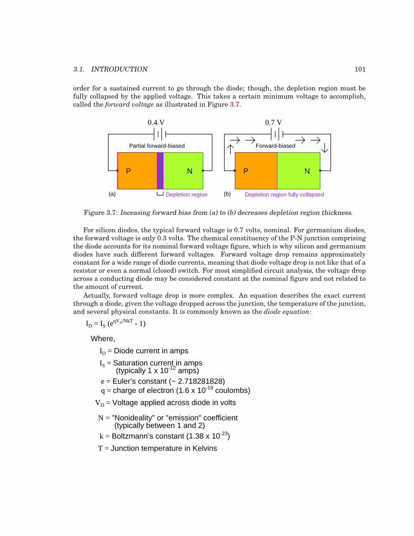
3.1. INTRODUCTION 101
order for a sustained current to go through the diode; though, the depletion region must befully collapsed by the applied voltage. This takes a certain minimum voltage to accomplish,called the forward voltage as illustrated in Figure 3.7.
0.4 V 0.7 V
P N P N
(b)
Partial forward-biased Forward-biased
Depletion region(a) Depletion region fully collapsed
Figure 3.7: Inceasing forward bias from (a) to (b) decreases depletion region thickness.
For silicon diodes, the typical forward voltage is 0.7 volts, nominal. For germanium diodes,the forward voltage is only 0.3 volts. The chemical constituency of the P-N junction comprisingthe diode accounts for its nominal forward voltage figure, which is why silicon and germaniumdiodes have such different forward voltages. Forward voltage drop remains approximatelyconstant for a wide range of diode currents, meaning that diode voltage drop is not like that of aresistor or even a normal (closed) switch. For most simplified circuit analysis, the voltage dropacross a conducting diode may be considered constant at the nominal figure and not related tothe amount of current.
Actually, forward voltage drop is more complex. An equation describes the exact currentthrough a diode, given the voltage dropped across the junction, the temperature of the junction,and several physical constants. It is commonly known as the diode equation:
ID = IS (eqVD/NkT - 1)
Where,
ID = Diode current in amps
IS = Saturation current in amps
e = Euler’s constant (~ 2.718281828)q = charge of electron (1.6 x 10⁻¹⁹ coulombs)
VD = Voltage applied across diode in volts
N = "Nonideality" or "emission" coefficient
(typically 1 x 10-12 amps)
(typically between 1 and 2)
T = Junction temperature in Kelvins
k = Boltzmann’s constant (1.38 x 10⁻²³)
102 CHAPTER 3. DIODES AND RECTIFIERS
The term kT/q describes the voltage produced within the P-N junction due to the action oftemperature, and is called the thermal voltage, or Vt of the junction. At room temperature,this is about 26 millivolts. Knowing this, and assuming a “nonideality” coefficient of 1, we maysimplify the diode equation and re-write it as such:
Where,
ID = Diode current in amps
IS = Saturation current in amps
e = Euler’s Number (~ 2.718281828)
VD = Voltage applied across diode in volts
(typically 1 x 10-12 amps)
ID = IS (eVD/0.026 -1)
You need not be familiar with the “diode equation” to analyze simple diode circuits. Justunderstand that the voltage dropped across a current-conducting diode does change with theamount of current going through it, but that this change is fairly small over a wide range ofcurrents. This is why many textbooks simply say the voltage drop across a conducting, semi-conductor diode remains constant at 0.7 volts for silicon and 0.3 volts for germanium. However,some circuits intentionally make use of the P-N junction’s inherent exponential current/voltagerelationship and thus can only be understood in the context of this equation. Also, since tem-perature is a factor in the diode equation, a forward-biased P-N junction may also be used as atemperature-sensing device, and thus can only be understood if one has a conceptual grasp onthis mathematical relationship.
A reverse-biased diode prevents current from going through it, due to the expanded deple-tion region. In actuality, a very small amount of current can and does go through a reverse-biased diode, called the leakage current, but it can be ignored for most purposes. The abilityof a diode to withstand reverse-bias voltages is limited, as it is for any insulator. If the ap-plied reverse-bias voltage becomes too great, the diode will experience a condition known asbreakdown (Figure 3.8), which is usually destructive. A diode’s maximum reverse-bias voltagerating is known as the Peak Inverse Voltage, or PIV, and may be obtained from the manufac-turer. Like forward voltage, the PIV rating of a diode varies with temperature, except thatPIV increases with increased temperature and decreases as the diode becomes cooler – exactlyopposite that of forward voltage.
Typically, the PIV rating of a generic “rectifier” diode is at least 50 volts at room tempera-ture. Diodes with PIV ratings in the many thousands of volts are available for modest prices.
• REVIEW:
• A diode is an electrical component acting as a one-way valve for current.
• When voltage is applied across a diode in such a way that the diode allows current, thediode is said to be forward-biased.
• When voltage is applied across a diode in such a way that the diode prohibits current, thediode is said to be reverse-biased.
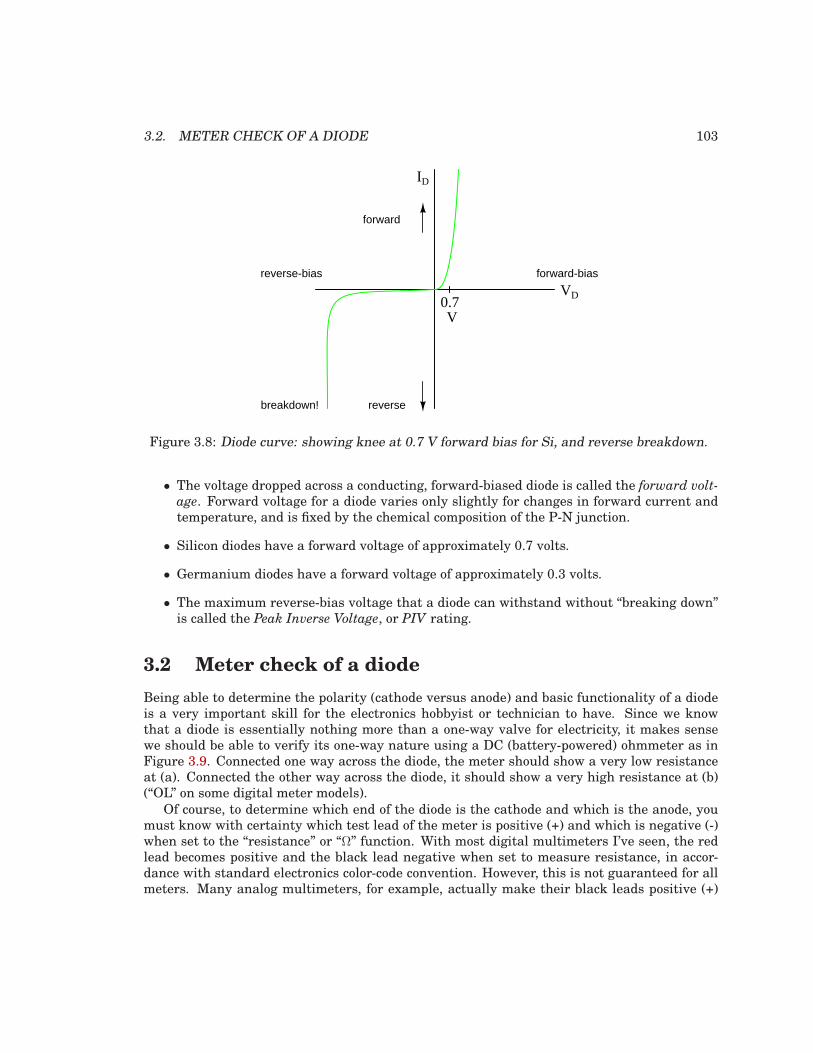
3.2. METER CHECK OF A DIODE 103
VD
ID
forward-biasreverse-bias
forward
reversebreakdown!
0.7V
Figure 3.8: Diode curve: showing knee at 0.7 V forward bias for Si, and reverse breakdown.
• The voltage dropped across a conducting, forward-biased diode is called the forward volt-
age. Forward voltage for a diode varies only slightly for changes in forward current andtemperature, and is fixed by the chemical composition of the P-N junction.
• Silicon diodes have a forward voltage of approximately 0.7 volts.
• Germanium diodes have a forward voltage of approximately 0.3 volts.
• The maximum reverse-bias voltage that a diode can withstand without “breaking down”is called the Peak Inverse Voltage, or PIV rating.
3.2 Meter check of a diode
Being able to determine the polarity (cathode versus anode) and basic functionality of a diodeis a very important skill for the electronics hobbyist or technician to have. Since we knowthat a diode is essentially nothing more than a one-way valve for electricity, it makes sensewe should be able to verify its one-way nature using a DC (battery-powered) ohmmeter as inFigure 3.9. Connected one way across the diode, the meter should show a very low resistanceat (a). Connected the other way across the diode, it should show a very high resistance at (b)(“OL” on some digital meter models).
Of course, to determine which end of the diode is the cathode and which is the anode, youmust know with certainty which test lead of the meter is positive (+) and which is negative (-)when set to the “resistance” or “Ω” function. With most digital multimeters I’ve seen, the redlead becomes positive and the black lead negative when set to measure resistance, in accor-dance with standard electronics color-code convention. However, this is not guaranteed for allmeters. Many analog multimeters, for example, actually make their black leads positive (+)
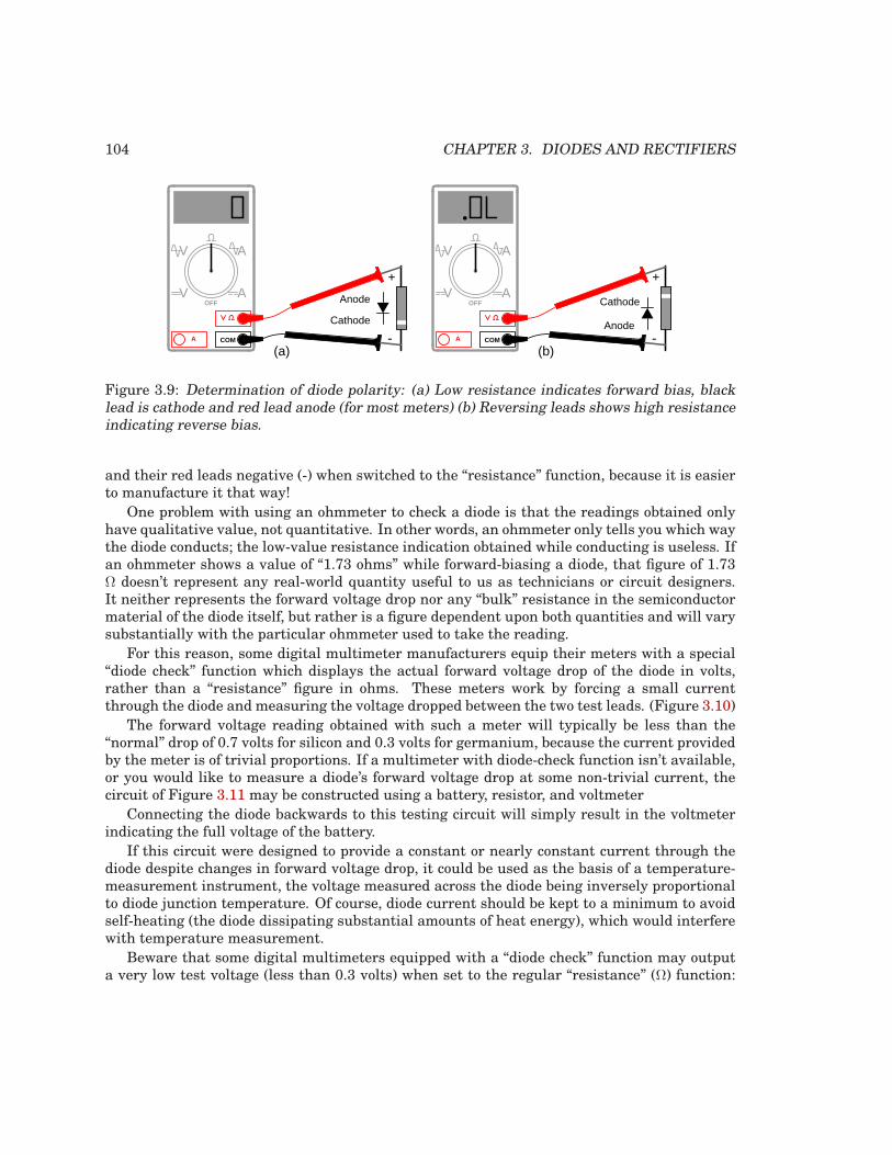
104 CHAPTER 3. DIODES AND RECTIFIERS
COMA
V
V A
AOFF Anode
Cathode
+
- COMA
V
V A
AOFF
Anode
Cathode
+
-(a) (b)
Figure 3.9: Determination of diode polarity: (a) Low resistance indicates forward bias, blacklead is cathode and red lead anode (for most meters) (b) Reversing leads shows high resistanceindicating reverse bias.
and their red leads negative (-) when switched to the “resistance” function, because it is easierto manufacture it that way!
One problem with using an ohmmeter to check a diode is that the readings obtained onlyhave qualitative value, not quantitative. In other words, an ohmmeter only tells you which waythe diode conducts; the low-value resistance indication obtained while conducting is useless. Ifan ohmmeter shows a value of “1.73 ohms” while forward-biasing a diode, that figure of 1.73Ω doesn’t represent any real-world quantity useful to us as technicians or circuit designers.It neither represents the forward voltage drop nor any “bulk” resistance in the semiconductormaterial of the diode itself, but rather is a figure dependent upon both quantities and will varysubstantially with the particular ohmmeter used to take the reading.
For this reason, some digital multimeter manufacturers equip their meters with a special“diode check” function which displays the actual forward voltage drop of the diode in volts,rather than a “resistance” figure in ohms. These meters work by forcing a small currentthrough the diode and measuring the voltage dropped between the two test leads. (Figure 3.10)
The forward voltage reading obtained with such a meter will typically be less than the“normal” drop of 0.7 volts for silicon and 0.3 volts for germanium, because the current providedby the meter is of trivial proportions. If a multimeter with diode-check function isn’t available,or you would like to measure a diode’s forward voltage drop at some non-trivial current, thecircuit of Figure 3.11 may be constructed using a battery, resistor, and voltmeter
Connecting the diode backwards to this testing circuit will simply result in the voltmeterindicating the full voltage of the battery.
If this circuit were designed to provide a constant or nearly constant current through thediode despite changes in forward voltage drop, it could be used as the basis of a temperature-measurement instrument, the voltage measured across the diode being inversely proportionalto diode junction temperature. Of course, diode current should be kept to a minimum to avoidself-heating (the diode dissipating substantial amounts of heat energy), which would interferewith temperature measurement.
Beware that some digital multimeters equipped with a “diode check” function may outputa very low test voltage (less than 0.3 volts) when set to the regular “resistance” (Ω) function:
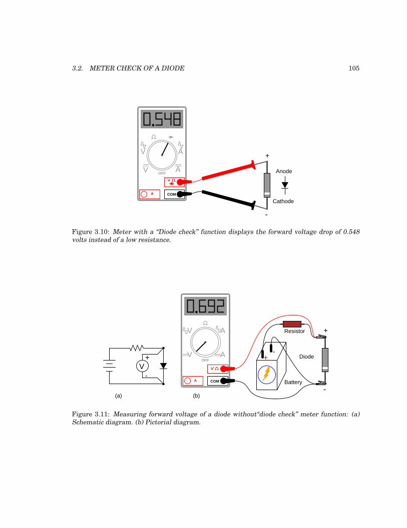
3.2. METER CHECK OF A DIODE 105
Anode
Cathode
+
-
OFF
COMA
V A
V A
Figure 3.10: Meter with a “Diode check” function displays the forward voltage drop of 0.548volts instead of a low resistance.
+
-COMA
V
V A
AOFF +
-
Resistor
Battery
+V
-
Diode
(a) (b)
Figure 3.11: Measuring forward voltage of a diode without“diode check” meter function: (a)Schematic diagram. (b) Pictorial diagram.
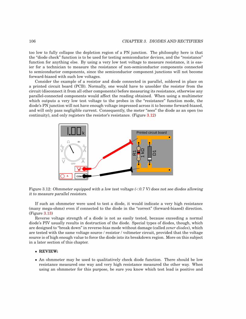
106 CHAPTER 3. DIODES AND RECTIFIERS
too low to fully collapse the depletion region of a PN junction. The philosophy here is thatthe “diode check” function is to be used for testing semiconductor devices, and the “resistance”function for anything else. By using a very low test voltage to measure resistance, it is eas-ier for a technician to measure the resistance of non-semiconductor components connectedto semiconductor components, since the semiconductor component junctions will not becomeforward-biased with such low voltages.
Consider the example of a resistor and diode connected in parallel, soldered in place ona printed circuit board (PCB). Normally, one would have to unsolder the resistor from thecircuit (disconnect it from all other components) before measuring its resistance, otherwise anyparallel-connected components would affect the reading obtained. When using a multimeterwhich outputs a very low test voltage to the probes in the “resistance” function mode, thediode’s PN junction will not have enough voltage impressed across it to become forward-biased,and will only pass negligible current. Consequently, the meter “sees” the diode as an open (nocontinuity), and only registers the resistor’s resistance. (Figure 3.12)
OFF
COMA
V A
V A
Printed circuit boardR
1
D1
1 kΩ
k
Figure 3.12: Ohmmeter equipped with a low test voltage (<0.7 V) does not see diodes allowingit to measure parallel resistors.
If such an ohmmeter were used to test a diode, it would indicate a very high resistance(many mega-ohms) even if connected to the diode in the “correct” (forward-biased) direction.(Figure 3.13)
Reverse voltage strength of a diode is not as easily tested, because exceeding a normaldiode’s PIV usually results in destruction of the diode. Special types of diodes, though, whichare designed to “break down” in reverse-bias mode without damage (called zener diodes), whichare tested with the same voltage source / resistor / voltmeter circuit, provided that the voltagesource is of high enough value to force the diode into its breakdown region. More on this subjectin a later section of this chapter.
• REVIEW:
• An ohmmeter may be used to qualitatively check diode function. There should be lowresistance measured one way and very high resistance measured the other way. Whenusing an ohmmeter for this purpose, be sure you know which test lead is positive and
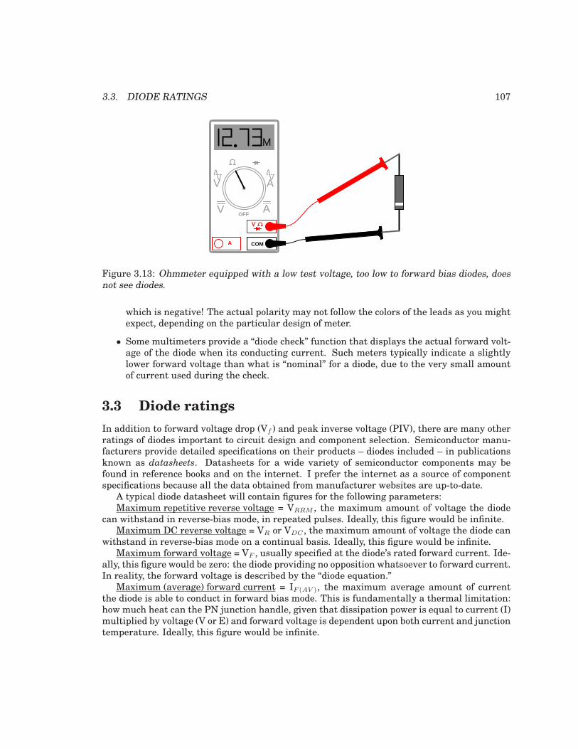
3.3. DIODE RATINGS 107
OFF
COMA
V A
V A
M
Figure 3.13: Ohmmeter equipped with a low test voltage, too low to forward bias diodes, doesnot see diodes.
which is negative! The actual polarity may not follow the colors of the leads as you mightexpect, depending on the particular design of meter.
• Some multimeters provide a “diode check” function that displays the actual forward volt-age of the diode when its conducting current. Such meters typically indicate a slightlylower forward voltage than what is “nominal” for a diode, due to the very small amountof current used during the check.
3.3 Diode ratings
In addition to forward voltage drop (Vf ) and peak inverse voltage (PIV), there are many otherratings of diodes important to circuit design and component selection. Semiconductor manu-facturers provide detailed specifications on their products – diodes included – in publicationsknown as datasheets. Datasheets for a wide variety of semiconductor components may befound in reference books and on the internet. I prefer the internet as a source of componentspecifications because all the data obtained from manufacturer websites are up-to-date.
A typical diode datasheet will contain figures for the following parameters:Maximum repetitive reverse voltage = VRRM , the maximum amount of voltage the diode
can withstand in reverse-bias mode, in repeated pulses. Ideally, this figure would be infinite.Maximum DC reverse voltage = VR or VDC , the maximum amount of voltage the diode can
withstand in reverse-bias mode on a continual basis. Ideally, this figure would be infinite.Maximum forward voltage = VF , usually specified at the diode’s rated forward current. Ide-
ally, this figure would be zero: the diode providing no opposition whatsoever to forward current.In reality, the forward voltage is described by the “diode equation.”
Maximum (average) forward current = IF (AV ), the maximum average amount of currentthe diode is able to conduct in forward bias mode. This is fundamentally a thermal limitation:how much heat can the PN junction handle, given that dissipation power is equal to current (I)multiplied by voltage (V or E) and forward voltage is dependent upon both current and junctiontemperature. Ideally, this figure would be infinite.
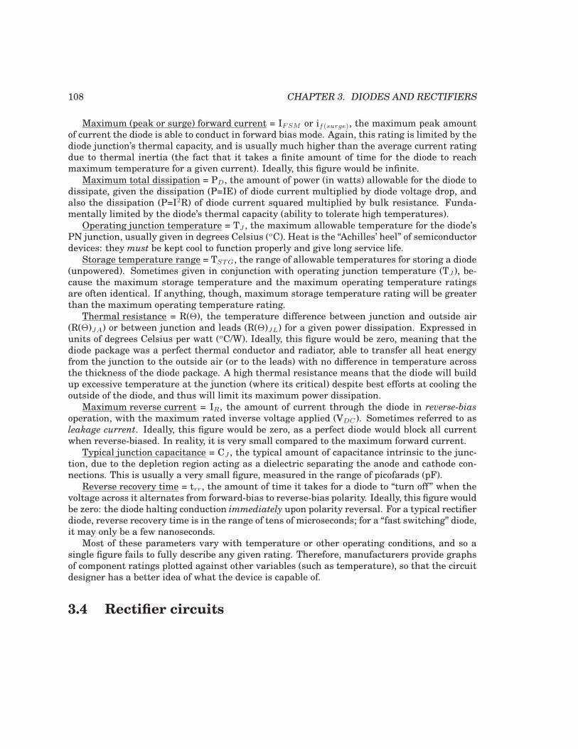
108 CHAPTER 3. DIODES AND RECTIFIERS
Maximum (peak or surge) forward current = IFSM or if(surge), the maximum peak amountof current the diode is able to conduct in forward bias mode. Again, this rating is limited by thediode junction’s thermal capacity, and is usually much higher than the average current ratingdue to thermal inertia (the fact that it takes a finite amount of time for the diode to reachmaximum temperature for a given current). Ideally, this figure would be infinite.
Maximum total dissipation = PD, the amount of power (in watts) allowable for the diode todissipate, given the dissipation (P=IE) of diode current multiplied by diode voltage drop, andalso the dissipation (P=I2R) of diode current squared multiplied by bulk resistance. Funda-mentally limited by the diode’s thermal capacity (ability to tolerate high temperatures).
Operating junction temperature = TJ , the maximum allowable temperature for the diode’sPN junction, usually given in degrees Celsius (oC). Heat is the “Achilles’ heel” of semiconductordevices: they must be kept cool to function properly and give long service life.
Storage temperature range = TSTG, the range of allowable temperatures for storing a diode(unpowered). Sometimes given in conjunction with operating junction temperature (TJ ), be-cause the maximum storage temperature and the maximum operating temperature ratingsare often identical. If anything, though, maximum storage temperature rating will be greaterthan the maximum operating temperature rating.
Thermal resistance = R(Θ), the temperature difference between junction and outside air(R(Θ)JA) or between junction and leads (R(Θ)JL) for a given power dissipation. Expressed inunits of degrees Celsius per watt (oC/W). Ideally, this figure would be zero, meaning that thediode package was a perfect thermal conductor and radiator, able to transfer all heat energyfrom the junction to the outside air (or to the leads) with no difference in temperature acrossthe thickness of the diode package. A high thermal resistance means that the diode will buildup excessive temperature at the junction (where its critical) despite best efforts at cooling theoutside of the diode, and thus will limit its maximum power dissipation.
Maximum reverse current = IR, the amount of current through the diode in reverse-bias
operation, with the maximum rated inverse voltage applied (VDC). Sometimes referred to asleakage current. Ideally, this figure would be zero, as a perfect diode would block all currentwhen reverse-biased. In reality, it is very small compared to the maximum forward current.
Typical junction capacitance = CJ , the typical amount of capacitance intrinsic to the junc-tion, due to the depletion region acting as a dielectric separating the anode and cathode con-nections. This is usually a very small figure, measured in the range of picofarads (pF).
Reverse recovery time = trr, the amount of time it takes for a diode to “turn off” when thevoltage across it alternates from forward-bias to reverse-bias polarity. Ideally, this figure wouldbe zero: the diode halting conduction immediately upon polarity reversal. For a typical rectifierdiode, reverse recovery time is in the range of tens of microseconds; for a “fast switching” diode,it may only be a few nanoseconds.
Most of these parameters vary with temperature or other operating conditions, and so asingle figure fails to fully describe any given rating. Therefore, manufacturers provide graphsof component ratings plotted against other variables (such as temperature), so that the circuitdesigner has a better idea of what the device is capable of.
3.4 Rectifier circuits
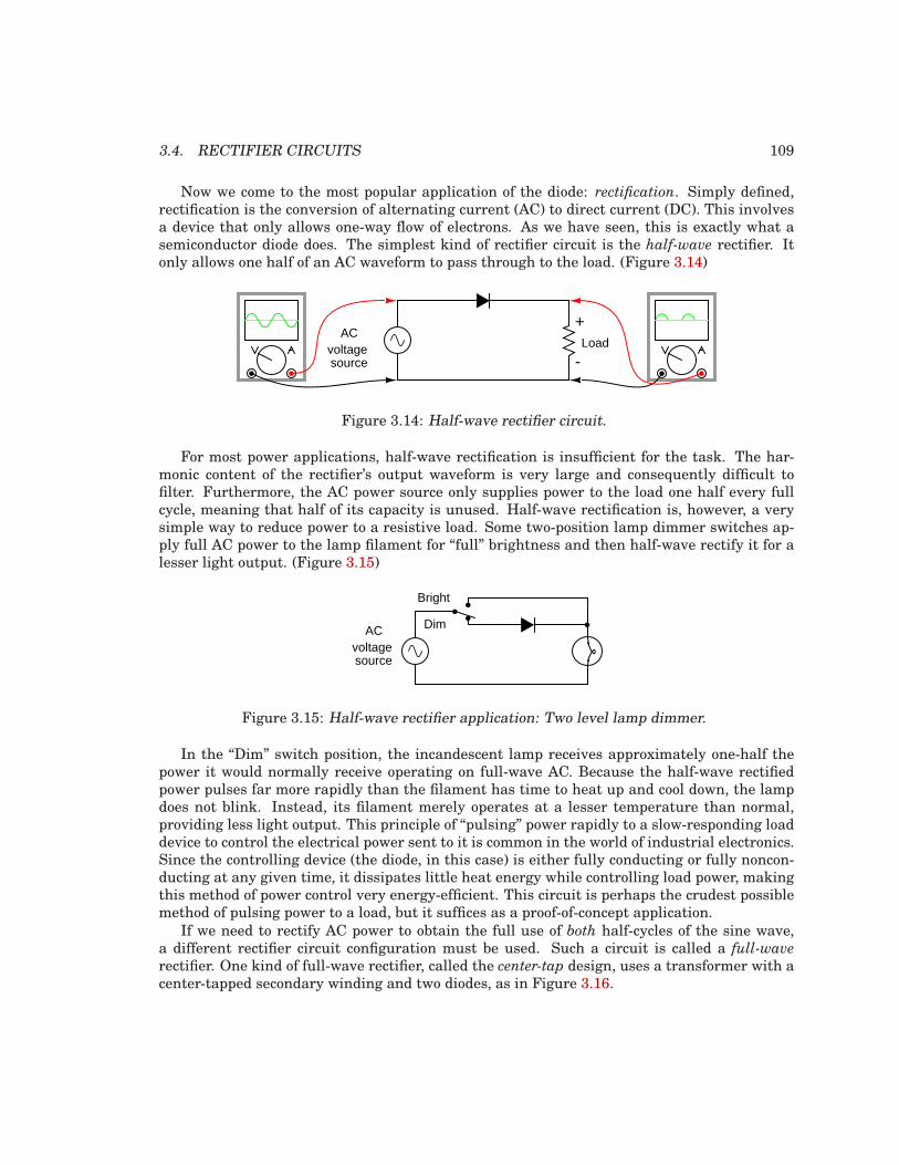
3.4. RECTIFIER CIRCUITS 109
Now we come to the most popular application of the diode: rectification. Simply defined,rectification is the conversion of alternating current (AC) to direct current (DC). This involvesa device that only allows one-way flow of electrons. As we have seen, this is exactly what asemiconductor diode does. The simplest kind of rectifier circuit is the half-wave rectifier. Itonly allows one half of an AC waveform to pass through to the load. (Figure 3.14)
LoadAC
voltagesource
+
-
Figure 3.14: Half-wave rectifier circuit.
For most power applications, half-wave rectification is insufficient for the task. The har-monic content of the rectifier’s output waveform is very large and consequently difficult tofilter. Furthermore, the AC power source only supplies power to the load one half every fullcycle, meaning that half of its capacity is unused. Half-wave rectification is, however, a verysimple way to reduce power to a resistive load. Some two-position lamp dimmer switches ap-ply full AC power to the lamp filament for “full” brightness and then half-wave rectify it for alesser light output. (Figure 3.15)
ACvoltagesource
Bright
Dim
Figure 3.15: Half-wave rectifier application: Two level lamp dimmer.
In the “Dim” switch position, the incandescent lamp receives approximately one-half thepower it would normally receive operating on full-wave AC. Because the half-wave rectifiedpower pulses far more rapidly than the filament has time to heat up and cool down, the lampdoes not blink. Instead, its filament merely operates at a lesser temperature than normal,providing less light output. This principle of “pulsing” power rapidly to a slow-responding loaddevice to control the electrical power sent to it is common in the world of industrial electronics.Since the controlling device (the diode, in this case) is either fully conducting or fully noncon-ducting at any given time, it dissipates little heat energy while controlling load power, makingthis method of power control very energy-efficient. This circuit is perhaps the crudest possiblemethod of pulsing power to a load, but it suffices as a proof-of-concept application.
If we need to rectify AC power to obtain the full use of both half-cycles of the sine wave,a different rectifier circuit configuration must be used. Such a circuit is called a full-wave
rectifier. One kind of full-wave rectifier, called the center-tap design, uses a transformer with acenter-tapped secondary winding and two diodes, as in Figure 3.16.
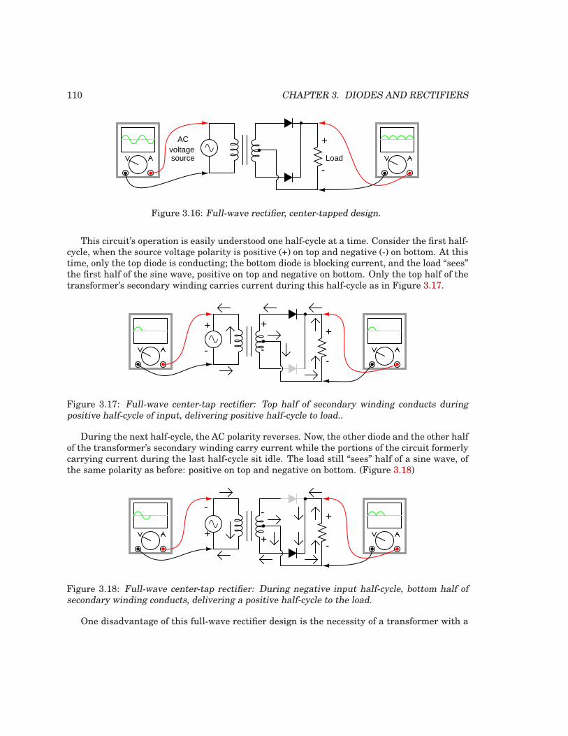
110 CHAPTER 3. DIODES AND RECTIFIERS
Load
ACvoltagesource
+
-
Figure 3.16: Full-wave rectifier, center-tapped design.
This circuit’s operation is easily understood one half-cycle at a time. Consider the first half-cycle, when the source voltage polarity is positive (+) on top and negative (-) on bottom. At thistime, only the top diode is conducting; the bottom diode is blocking current, and the load “sees”the first half of the sine wave, positive on top and negative on bottom. Only the top half of thetransformer’s secondary winding carries current during this half-cycle as in Figure 3.17.
+
-
+
-
+
-
Figure 3.17: Full-wave center-tap rectifier: Top half of secondary winding conducts duringpositive half-cycle of input, delivering positive half-cycle to load..
During the next half-cycle, the AC polarity reverses. Now, the other diode and the other halfof the transformer’s secondary winding carry current while the portions of the circuit formerlycarrying current during the last half-cycle sit idle. The load still “sees” half of a sine wave, ofthe same polarity as before: positive on top and negative on bottom. (Figure 3.18)
+
-+
-
+
-
Figure 3.18: Full-wave center-tap rectifier: During negative input half-cycle, bottom half ofsecondary winding conducts, delivering a positive half-cycle to the load.
One disadvantage of this full-wave rectifier design is the necessity of a transformer with a
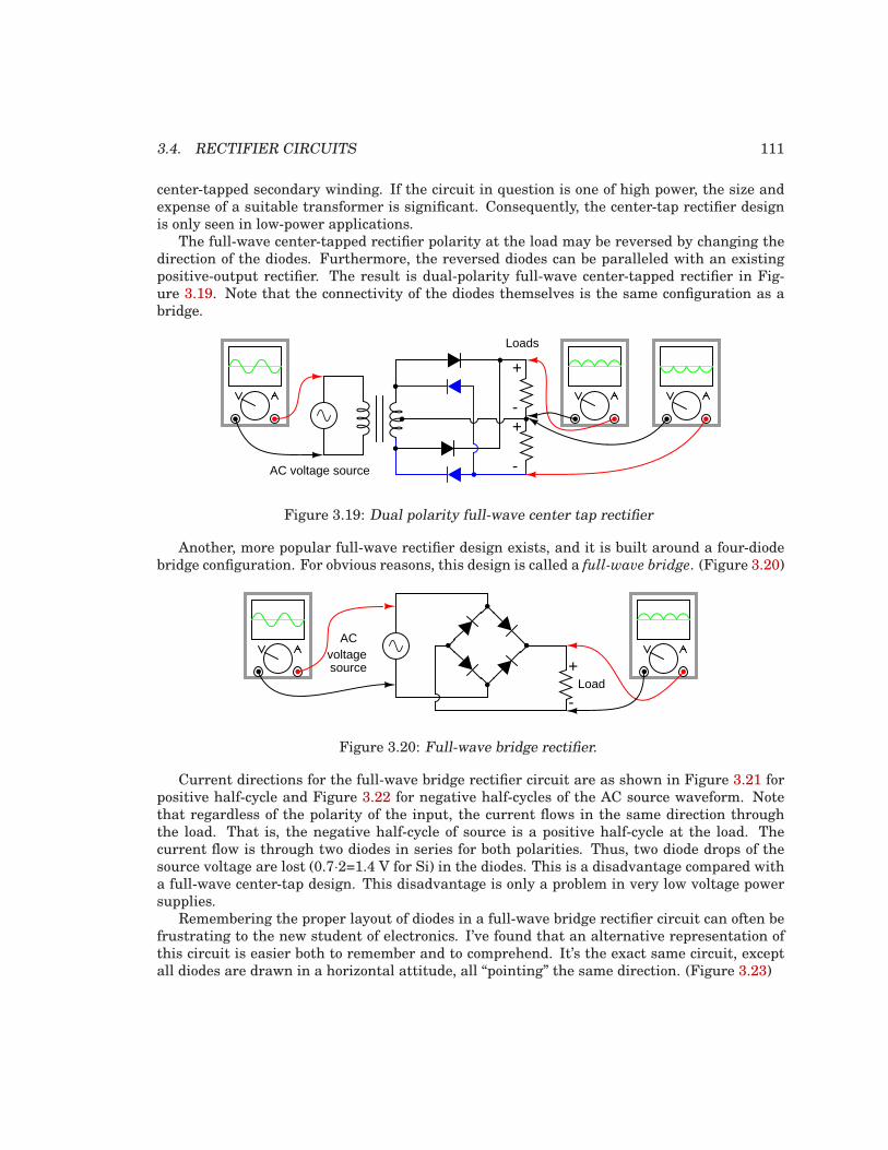
3.4. RECTIFIER CIRCUITS 111
center-tapped secondary winding. If the circuit in question is one of high power, the size andexpense of a suitable transformer is significant. Consequently, the center-tap rectifier designis only seen in low-power applications.
The full-wave center-tapped rectifier polarity at the load may be reversed by changing thedirection of the diodes. Furthermore, the reversed diodes can be paralleled with an existingpositive-output rectifier. The result is dual-polarity full-wave center-tapped rectifier in Fig-ure 3.19. Note that the connectivity of the diodes themselves is the same configuration as abridge.
+
+
-
-
Loads
AC voltage source
Figure 3.19: Dual polarity full-wave center tap rectifier
Another, more popular full-wave rectifier design exists, and it is built around a four-diodebridge configuration. For obvious reasons, this design is called a full-wave bridge. (Figure 3.20)
Load
ACvoltagesource +
-
Figure 3.20: Full-wave bridge rectifier.
Current directions for the full-wave bridge rectifier circuit are as shown in Figure 3.21 forpositive half-cycle and Figure 3.22 for negative half-cycles of the AC source waveform. Notethat regardless of the polarity of the input, the current flows in the same direction throughthe load. That is, the negative half-cycle of source is a positive half-cycle at the load. Thecurrent flow is through two diodes in series for both polarities. Thus, two diode drops of thesource voltage are lost (0.7·2=1.4 V for Si) in the diodes. This is a disadvantage compared witha full-wave center-tap design. This disadvantage is only a problem in very low voltage powersupplies.
Remembering the proper layout of diodes in a full-wave bridge rectifier circuit can often befrustrating to the new student of electronics. I’ve found that an alternative representation ofthis circuit is easier both to remember and to comprehend. It’s the exact same circuit, exceptall diodes are drawn in a horizontal attitude, all “pointing” the same direction. (Figure 3.23)
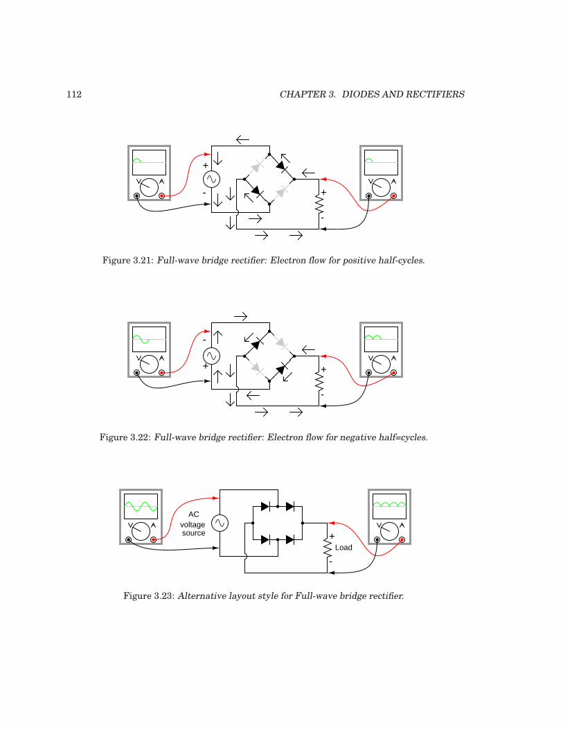
112 CHAPTER 3. DIODES AND RECTIFIERS
+
-
+
-
Figure 3.21: Full-wave bridge rectifier: Electron flow for positive half-cycles.
+
-
+
-
Figure 3.22: Full-wave bridge rectifier: Electron flow for negative half=cycles.
Load
ACvoltagesource +
-
Figure 3.23: Alternative layout style for Full-wave bridge rectifier.
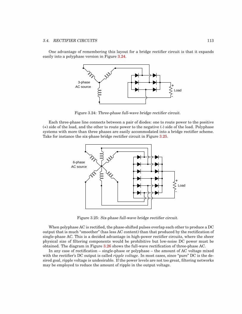
3.4. RECTIFIER CIRCUITS 113
One advantage of remembering this layout for a bridge rectifier circuit is that it expandseasily into a polyphase version in Figure 3.24.
Load+
-
3-phaseAC source
Figure 3.24: Three-phase full-wave bridge rectifier circuit.
Each three-phase line connects between a pair of diodes: one to route power to the positive(+) side of the load, and the other to route power to the negative (-) side of the load. Polyphasesystems with more than three phases are easily accommodated into a bridge rectifier scheme.Take for instance the six-phase bridge rectifier circuit in Figure 3.25.
Load+
-
AC source6-phase
Figure 3.25: Six-phase full-wave bridge rectifier circuit.
When polyphase AC is rectified, the phase-shifted pulses overlap each other to produce a DCoutput that is much “smoother” (has less AC content) than that produced by the rectification ofsingle-phase AC. This is a decided advantage in high-power rectifier circuits, where the sheerphysical size of filtering components would be prohibitive but low-noise DC power must beobtained. The diagram in Figure 3.26 shows the full-wave rectification of three-phase AC.
In any case of rectification – single-phase or polyphase – the amount of AC voltage mixedwith the rectifier’s DC output is called ripple voltage. In most cases, since “pure” DC is the de-sired goal, ripple voltage is undesirable. If the power levels are not too great, filtering networksmay be employed to reduce the amount of ripple in the output voltage.
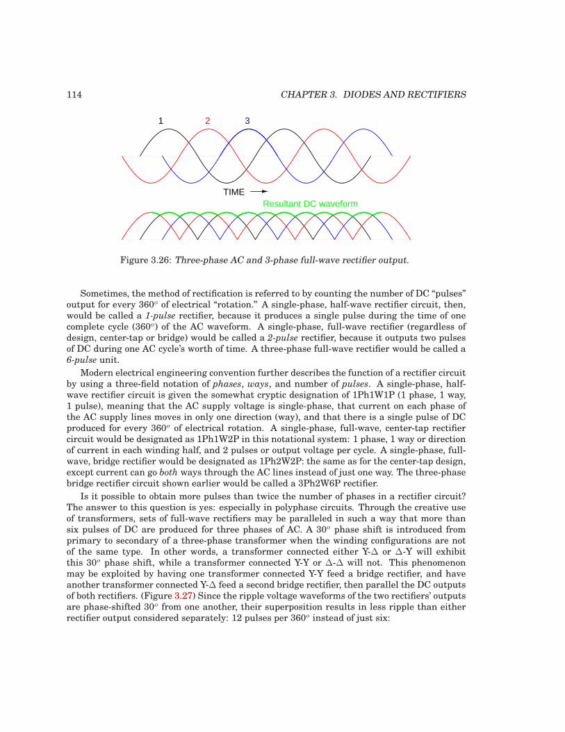
114 CHAPTER 3. DIODES AND RECTIFIERS
1 2 3
TIME Resultant DC waveform
Figure 3.26: Three-phase AC and 3-phase full-wave rectifier output.
Sometimes, the method of rectification is referred to by counting the number of DC “pulses”output for every 360o of electrical “rotation.” A single-phase, half-wave rectifier circuit, then,would be called a 1-pulse rectifier, because it produces a single pulse during the time of onecomplete cycle (360o) of the AC waveform. A single-phase, full-wave rectifier (regardless ofdesign, center-tap or bridge) would be called a 2-pulse rectifier, because it outputs two pulsesof DC during one AC cycle’s worth of time. A three-phase full-wave rectifier would be called a6-pulse unit.
Modern electrical engineering convention further describes the function of a rectifier circuitby using a three-field notation of phases, ways, and number of pulses. A single-phase, half-wave rectifier circuit is given the somewhat cryptic designation of 1Ph1W1P (1 phase, 1 way,1 pulse), meaning that the AC supply voltage is single-phase, that current on each phase ofthe AC supply lines moves in only one direction (way), and that there is a single pulse of DCproduced for every 360o of electrical rotation. A single-phase, full-wave, center-tap rectifiercircuit would be designated as 1Ph1W2P in this notational system: 1 phase, 1 way or directionof current in each winding half, and 2 pulses or output voltage per cycle. A single-phase, full-wave, bridge rectifier would be designated as 1Ph2W2P: the same as for the center-tap design,except current can go both ways through the AC lines instead of just one way. The three-phasebridge rectifier circuit shown earlier would be called a 3Ph2W6P rectifier.
Is it possible to obtain more pulses than twice the number of phases in a rectifier circuit?The answer to this question is yes: especially in polyphase circuits. Through the creative useof transformers, sets of full-wave rectifiers may be paralleled in such a way that more thansix pulses of DC are produced for three phases of AC. A 30o phase shift is introduced fromprimary to secondary of a three-phase transformer when the winding configurations are notof the same type. In other words, a transformer connected either Y-∆ or ∆-Y will exhibitthis 30o phase shift, while a transformer connected Y-Y or ∆-∆ will not. This phenomenonmay be exploited by having one transformer connected Y-Y feed a bridge rectifier, and haveanother transformer connected Y-∆ feed a second bridge rectifier, then parallel the DC outputsof both rectifiers. (Figure 3.27) Since the ripple voltage waveforms of the two rectifiers’ outputsare phase-shifted 30o from one another, their superposition results in less ripple than eitherrectifier output considered separately: 12 pulses per 360o instead of just six:
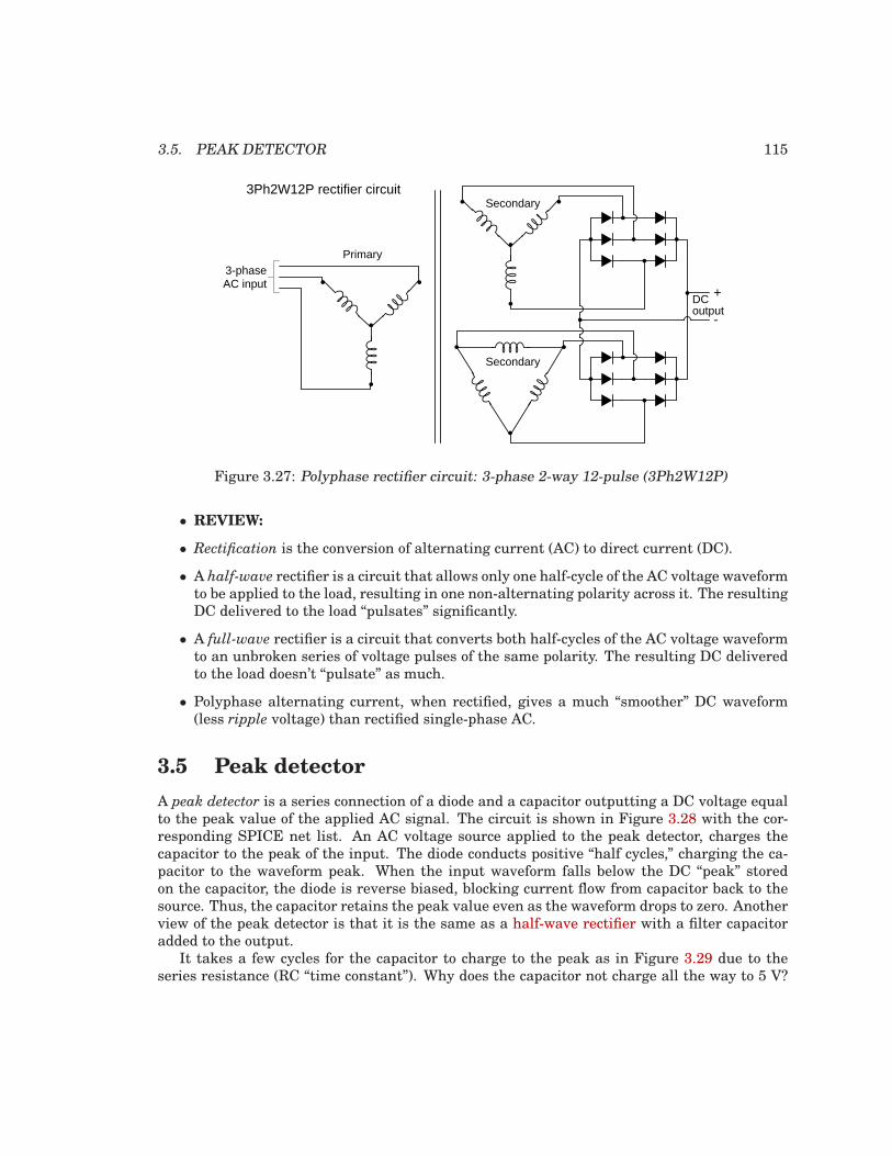
3.5. PEAK DETECTOR 115
+
-
DC output
3-phaseAC input
Primary
Secondary
Secondary
3Ph2W12P rectifier circuit
Figure 3.27: Polyphase rectifier circuit: 3-phase 2-way 12-pulse (3Ph2W12P)
• REVIEW:
• Rectification is the conversion of alternating current (AC) to direct current (DC).
• A half-wave rectifier is a circuit that allows only one half-cycle of the AC voltage waveformto be applied to the load, resulting in one non-alternating polarity across it. The resultingDC delivered to the load “pulsates” significantly.
• A full-wave rectifier is a circuit that converts both half-cycles of the AC voltage waveformto an unbroken series of voltage pulses of the same polarity. The resulting DC deliveredto the load doesn’t “pulsate” as much.
• Polyphase alternating current, when rectified, gives a much “smoother” DC waveform(less ripple voltage) than rectified single-phase AC.
3.5 Peak detector
A peak detector is a series connection of a diode and a capacitor outputting a DC voltage equalto the peak value of the applied AC signal. The circuit is shown in Figure 3.28 with the cor-responding SPICE net list. An AC voltage source applied to the peak detector, charges thecapacitor to the peak of the input. The diode conducts positive “half cycles,” charging the ca-pacitor to the waveform peak. When the input waveform falls below the DC “peak” storedon the capacitor, the diode is reverse biased, blocking current flow from capacitor back to thesource. Thus, the capacitor retains the peak value even as the waveform drops to zero. Anotherview of the peak detector is that it is the same as a half-wave rectifier with a filter capacitoradded to the output.
It takes a few cycles for the capacitor to charge to the peak as in Figure 3.29 due to theseries resistance (RC “time constant”). Why does the capacitor not charge all the way to 5 V?
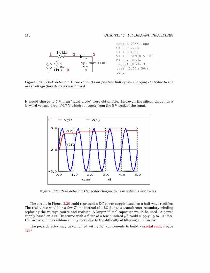
116 CHAPTER 3. DIODES AND RECTIFIERS
5 Vp-p0 Voffset1 kHz
1.0kΩ
0.1uF
1
0
23
V(2)output
* SPICE 03441.epsC1 2 0 0.1uR1 1 3 1.0kV1 1 0 SIN(0 5 1k)D1 3 2 diode.model diode d.tran 0.01m 50mm.end
Figure 3.28: Peak detector: Diode conducts on positive half cycles charging capacitor to thepeak voltage (less diode forward drop).
It would charge to 5 V if an “ideal diode” were obtainable. However, the silicon diode has aforward voltage drop of 0.7 V which subtracts from the 5 V peak of the input.
Figure 3.29: Peak detector: Capacitor charges to peak within a few cycles.
The circuit in Figure 3.28 could represent a DC power supply based on a half-wave rectifier.The resistance would be a few Ohms instead of 1 kΩ due to a transformer secondary windingreplacing the voltage source and resistor. A larger “filter” capacitor would be used. A powersupply based on a 60 Hz source with a filter of a few hundred µF could supply up to 100 mA.Half-wave supplies seldom supply more due to the difficulty of filtering a half-wave.
The peak detector may be combined with other components to build a crystal radio ( page426).
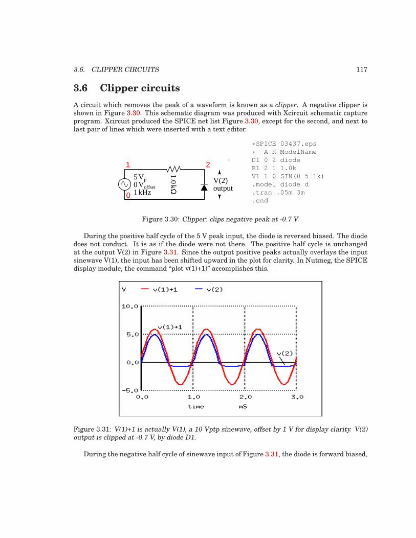
3.6. CLIPPER CIRCUITS 117
3.6 Clipper circuits
A circuit which removes the peak of a waveform is known as a clipper. A negative clipper isshown in Figure 3.30. This schematic diagram was produced with Xcircuit schematic captureprogram. Xcircuit produced the SPICE net list Figure 3.30, except for the second, and next tolast pair of lines which were inserted with a text editor.
5 Vp0 Voffset1 kHz
1.0kΩ
0
1 2
V(2)output
* SPICE 03437.eps
* A K ModelNameD1 0 2 diodeR1 2 1 1.0kV1 1 0 SIN(0 5 1k).model diode d.tran .05m 3m.end
Figure 3.30: Clipper: clips negative peak at -0.7 V.
During the positive half cycle of the 5 V peak input, the diode is reversed biased. The diodedoes not conduct. It is as if the diode were not there. The positive half cycle is unchangedat the output V(2) in Figure 3.31. Since the output positive peaks actually overlays the inputsinewave V(1), the input has been shifted upward in the plot for clarity. In Nutmeg, the SPICEdisplay module, the command “plot v(1)+1)” accomplishes this.
Figure 3.31: V(1)+1 is actually V(1), a 10 Vptp sinewave, offset by 1 V for display clarity. V(2)output is clipped at -0.7 V, by diode D1.
During the negative half cycle of sinewave input of Figure 3.31, the diode is forward biased,
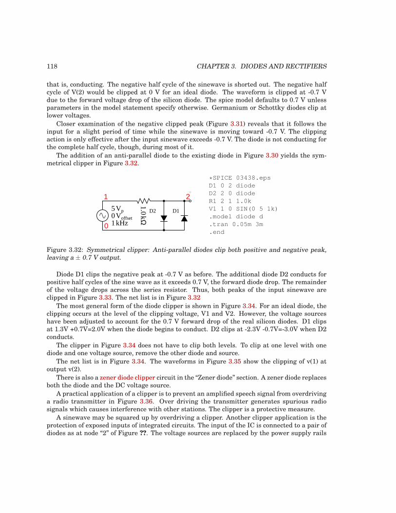
118 CHAPTER 3. DIODES AND RECTIFIERS
that is, conducting. The negative half cycle of the sinewave is shorted out. The negative halfcycle of V(2) would be clipped at 0 V for an ideal diode. The waveform is clipped at -0.7 Vdue to the forward voltage drop of the silicon diode. The spice model defaults to 0.7 V unlessparameters in the model statement specify otherwise. Germanium or Schottky diodes clip atlower voltages.
Closer examination of the negative clipped peak (Figure 3.31) reveals that it follows theinput for a slight period of time while the sinewave is moving toward -0.7 V. The clippingaction is only effective after the input sinewave exceeds -0.7 V. The diode is not conducting forthe complete half cycle, though, during most of it.
The addition of an anti-parallel diode to the existing diode in Figure 3.30 yields the sym-metrical clipper in Figure 3.32.
5 Vp0 Voffset1 kHz
1.0kΩ
0
1 2
D2 D1
* SPICE 03438.epsD1 0 2 diodeD2 2 0 diodeR1 2 1 1.0kV1 1 0 SIN(0 5 1k).model diode d.tran 0.05m 3m.end
Figure 3.32: Symmetrical clipper: Anti-parallel diodes clip both positive and negative peak,leaving a ± 0.7 V output.
Diode D1 clips the negative peak at -0.7 V as before. The additional diode D2 conducts forpositive half cycles of the sine wave as it exceeds 0.7 V, the forward diode drop. The remainderof the voltage drops across the series resistor. Thus, both peaks of the input sinewave areclipped in Figure 3.33. The net list is in Figure 3.32
The most general form of the diode clipper is shown in Figure 3.34. For an ideal diode, theclipping occurs at the level of the clipping voltage, V1 and V2. However, the voltage sourceshave been adjusted to account for the 0.7 V forward drop of the real silicon diodes. D1 clipsat 1.3V +0.7V=2.0V when the diode begins to conduct. D2 clips at -2.3V -0.7V=-3.0V when D2conducts.
The clipper in Figure 3.34 does not have to clip both levels. To clip at one level with onediode and one voltage source, remove the other diode and source.
The net list is in Figure 3.34. The waveforms in Figure 3.35 show the clipping of v(1) atoutput v(2).
There is also a zener diode clipper circuit in the “Zener diode” section. A zener diode replacesboth the diode and the DC voltage source.
A practical application of a clipper is to prevent an amplified speech signal from overdrivinga radio transmitter in Figure 3.36. Over driving the transmitter generates spurious radiosignals which causes interference with other stations. The clipper is a protective measure.
A sinewave may be squared up by overdriving a clipper. Another clipper application is theprotection of exposed inputs of integrated circuits. The input of the IC is connected to a pair ofdiodes as at node “2” of Figure ??. The voltage sources are replaced by the power supply rails
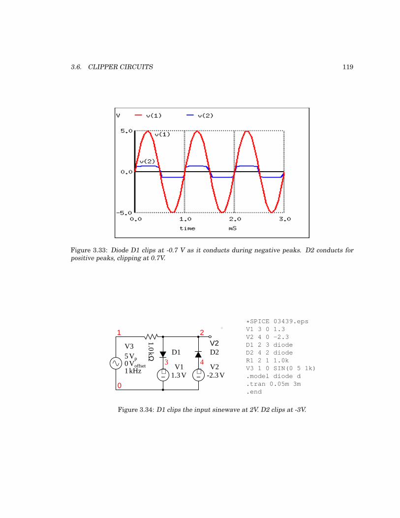
3.6. CLIPPER CIRCUITS 119
Figure 3.33: Diode D1 clips at -0.7 V as it conducts during negative peaks. D2 conducts forpositive peaks, clipping at 0.7V.
5Vp0Voffset1kHz
1.0kΩ
0
1 2
+− -2.3V+
− 1.3V
3 4D1
V1 V2
D2V3 V2
* SPICE 03439.epsV1 3 0 1.3V2 4 0 -2.3D1 2 3 diodeD2 4 2 diodeR1 2 1 1.0kV3 1 0 SIN(0 5 1k).model diode d.tran 0.05m 3m.end
Figure 3.34: D1 clips the input sinewave at 2V. D2 clips at -3V.
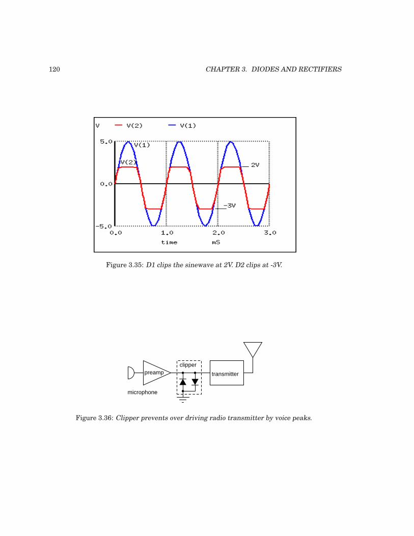
120 CHAPTER 3. DIODES AND RECTIFIERS
Figure 3.35: D1 clips the sinewave at 2V. D2 clips at -3V.
microphone
preampclipper
transmitter
Figure 3.36: Clipper prevents over driving radio transmitter by voice peaks.
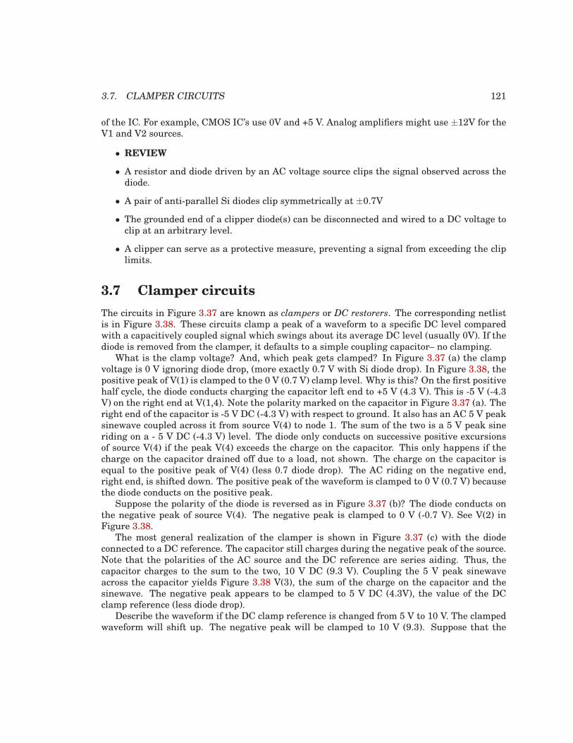
3.7. CLAMPER CIRCUITS 121
of the IC. For example, CMOS IC’s use 0V and +5 V. Analog amplifiers might use ±12V for theV1 and V2 sources.
• REVIEW
• A resistor and diode driven by an AC voltage source clips the signal observed across thediode.
• A pair of anti-parallel Si diodes clip symmetrically at ±0.7V
• The grounded end of a clipper diode(s) can be disconnected and wired to a DC voltage toclip at an arbitrary level.
• A clipper can serve as a protective measure, preventing a signal from exceeding the cliplimits.
3.7 Clamper circuits
The circuits in Figure 3.37 are known as clampers or DC restorers. The corresponding netlistis in Figure 3.38. These circuits clamp a peak of a waveform to a specific DC level comparedwith a capacitively coupled signal which swings about its average DC level (usually 0V). If thediode is removed from the clamper, it defaults to a simple coupling capacitor– no clamping.
What is the clamp voltage? And, which peak gets clamped? In Figure 3.37 (a) the clampvoltage is 0 V ignoring diode drop, (more exactly 0.7 V with Si diode drop). In Figure 3.38, thepositive peak of V(1) is clamped to the 0 V (0.7 V) clamp level. Why is this? On the first positivehalf cycle, the diode conducts charging the capacitor left end to +5 V (4.3 V). This is -5 V (-4.3V) on the right end at V(1,4). Note the polarity marked on the capacitor in Figure 3.37 (a). Theright end of the capacitor is -5 V DC (-4.3 V) with respect to ground. It also has an AC 5 V peaksinewave coupled across it from source V(4) to node 1. The sum of the two is a 5 V peak sineriding on a - 5 V DC (-4.3 V) level. The diode only conducts on successive positive excursionsof source V(4) if the peak V(4) exceeds the charge on the capacitor. This only happens if thecharge on the capacitor drained off due to a load, not shown. The charge on the capacitor isequal to the positive peak of V(4) (less 0.7 diode drop). The AC riding on the negative end,right end, is shifted down. The positive peak of the waveform is clamped to 0 V (0.7 V) becausethe diode conducts on the positive peak.
Suppose the polarity of the diode is reversed as in Figure 3.37 (b)? The diode conducts onthe negative peak of source V(4). The negative peak is clamped to 0 V (-0.7 V). See V(2) inFigure 3.38.
The most general realization of the clamper is shown in Figure 3.37 (c) with the diodeconnected to a DC reference. The capacitor still charges during the negative peak of the source.Note that the polarities of the AC source and the DC reference are series aiding. Thus, thecapacitor charges to the sum to the two, 10 V DC (9.3 V). Coupling the 5 V peak sinewaveacross the capacitor yields Figure 3.38 V(3), the sum of the charge on the capacitor and thesinewave. The negative peak appears to be clamped to 5 V DC (4.3V), the value of the DCclamp reference (less diode drop).
Describe the waveform if the DC clamp reference is changed from 5 V to 10 V. The clampedwaveform will shift up. The negative peak will be clamped to 10 V (9.3). Suppose that the
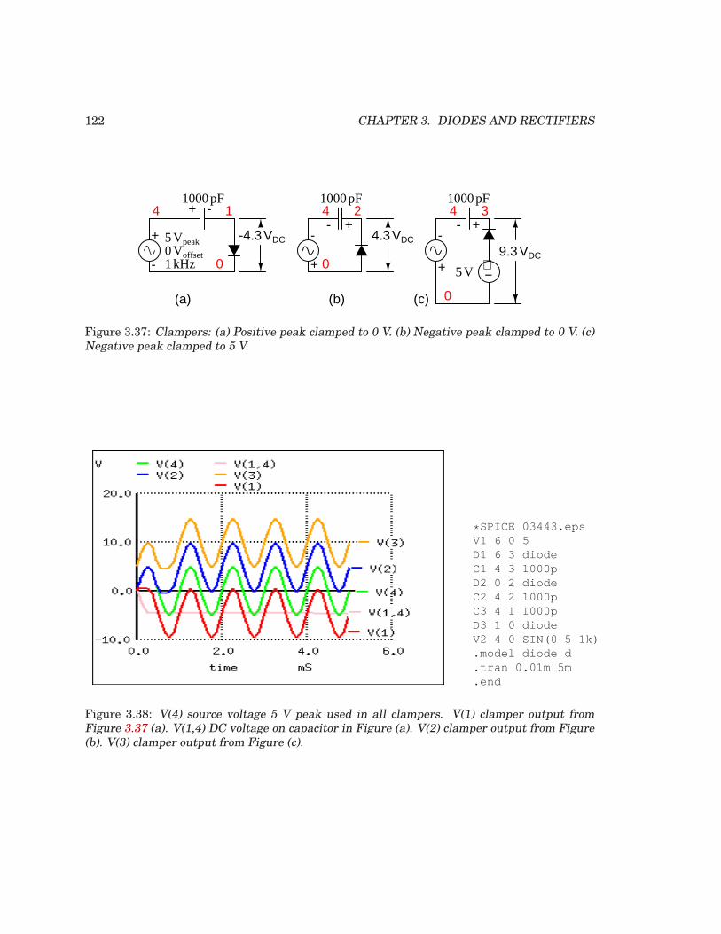
122 CHAPTER 3. DIODES AND RECTIFIERS
5 Vpeak0 Voffset1 kHz 0
4 11000pF4
0
2 41000pF
0
3
+−5V
(a) (b) (c)
+
-
+ -1000pF
+ +
+- -
-- +-4.3VDC
9.3 VDC
4.3VDC
Figure 3.37: Clampers: (a) Positive peak clamped to 0 V. (b) Negative peak clamped to 0 V. (c)Negative peak clamped to 5 V.
* SPICE 03443.epsV1 6 0 5D1 6 3 diodeC1 4 3 1000pD2 0 2 diodeC2 4 2 1000pC3 4 1 1000pD3 1 0 diodeV2 4 0 SIN(0 5 1k).model diode d.tran 0.01m 5m.end
Figure 3.38: V(4) source voltage 5 V peak used in all clampers. V(1) clamper output fromFigure 3.37 (a). V(1,4) DC voltage on capacitor in Figure (a). V(2) clamper output from Figure(b). V(3) clamper output from Figure (c).
3.8. VOLTAGE MULTIPLIERS 123
amplitude of the sine wave source is increased from 5 V to 7 V? The negative peak clamp levelwill remain unchanged. Though, the amplitude of the sinewave output will increase.
An application of the clamper circuit is as a “DC restorer” in “composite video” circuitry inboth television transmitters and receivers. An NTSC (US video standard) video signal “whitelevel” corresponds to minimum (12.5%) transmitted power. The video “black level” correspondsto a high level (75% of transmitter power. There is a “blacker than black level” corresponding to100% transmitted power assigned to synchronization signals. The NTSC signal contains bothvideo and synchronization pulses. The problem with the composite video is that its averageDC level varies with the scene, dark vs light. The video itself is supposed to vary. However,the sync must always peak at 100%. To prevent the sync signals from drifting with changingscenes, a “DC restorer” clamps the top of the sync pulses to a voltage corresponding to 100%transmitter modulation. [2]
• REVIEW:
• A capacitively coupled signal alternates about its average DC level (0 V).
• The signal out of a clamper appears the have one peak clamped to a DC voltage. Example:The negative peak is clamped to 0 VDC, the waveform appears to be shifted upward. Thepolarity of the diode determines which peak is clamped.
• An application of a clamper, or DC restorer, is in clamping the sync pulses of compositevideo to a voltage corresponding to 100% of transmitter power.
3.8 Voltage multipliers
A voltage multiplier is a specialized rectifier circuit producing an output which is theoreticallyan integer times the AC peak input, for example, 2, 3, or 4 times the AC peak input. Thus,it is possible to get 200 VDC from a 100 Vpeak AC source using a doubler, 400 VDC from aquadrupler. Any load in a practical circuit will lower these voltages.
A voltage doubler application is a DC power supply capable of using either a 240 VAC or 120VAC source. The supply uses a switch selected full-wave bridge to produce about 300 VDC froma 240 VAC source. The 120 V position of the switch rewires the bridge as a doubler producingabout 300 VDC from the 120 VAC. In both cases, 300 VDC is produced. This is the input to aswitching regulator producing lower voltages for powering, say, a personal computer.
The half-wave voltage doubler in Figure 3.39 (a) is composed of two circuits: a clamper at(b) and peak detector (half-wave rectifier) in Figure 3.28, which is shown in modified form inFigure 3.39 (c). C2 has been added to a peak detector (half-wave rectifier).
Referring to Figure 3.39 (b), C2 charges to 5 V (4.3 V considering the diode drop) on thenegative half cycle of AC input. The right end is grounded by the conducting D2. The left endis charged at the negative peak of the AC input. This is the operation of the clamper.
During the positive half cycle, the half-wave rectifier comes into play at Figure 3.39 (c).Diode D2 is out of the circuit since it is reverse biased. C2 is now in series with the voltagesource. Note the polarities of the generator and C2, series aiding. Thus, rectifier D1 sees a totalof 10 V at the peak of the sinewave, 5 V from generator and 5 V from C2. D1 conducts waveformv(1) (Figure 3.40), charging C1 to the peak of the sine wave riding on 5 V DC (Figure 3.40 v(2)).
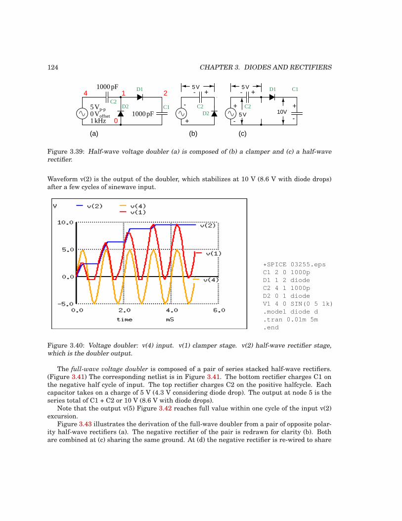
124 CHAPTER 3. DIODES AND RECTIFIERS
5Vp-p0Voffset1kHz 0
4 1
(a)
1000pF
1000pF
2
+
-
+-5 V
+
-
+-
10V5 V
5V
-
+
(b) (c)
C2D2
C1
D1
C2C2
D2
D1 C1
Figure 3.39: Half-wave voltage doubler (a) is composed of (b) a clamper and (c) a half-waverectifier.
Waveform v(2) is the output of the doubler, which stabilizes at 10 V (8.6 V with diode drops)after a few cycles of sinewave input.
* SPICE 03255.epsC1 2 0 1000pD1 1 2 diodeC2 4 1 1000pD2 0 1 diodeV1 4 0 SIN(0 5 1k).model diode d.tran 0.01m 5m.end
Figure 3.40: Voltage doubler: v(4) input. v(1) clamper stage. v(2) half-wave rectifier stage,which is the doubler output.
The full-wave voltage doubler is composed of a pair of series stacked half-wave rectifiers.(Figure 3.41) The corresponding netlist is in Figure 3.41. The bottom rectifier charges C1 onthe negative half cycle of input. The top rectifier charges C2 on the positive halfcycle. Eachcapacitor takes on a charge of 5 V (4.3 V considering diode drop). The output at node 5 is theseries total of C1 + C2 or 10 V (8.6 V with diode drops).
Note that the output v(5) Figure 3.42 reaches full value within one cycle of the input v(2)excursion.
Figure 3.43 illustrates the derivation of the full-wave doubler from a pair of opposite polar-ity half-wave rectifiers (a). The negative rectifier of the pair is redrawn for clarity (b). Bothare combined at (c) sharing the same ground. At (d) the negative rectifier is re-wired to share
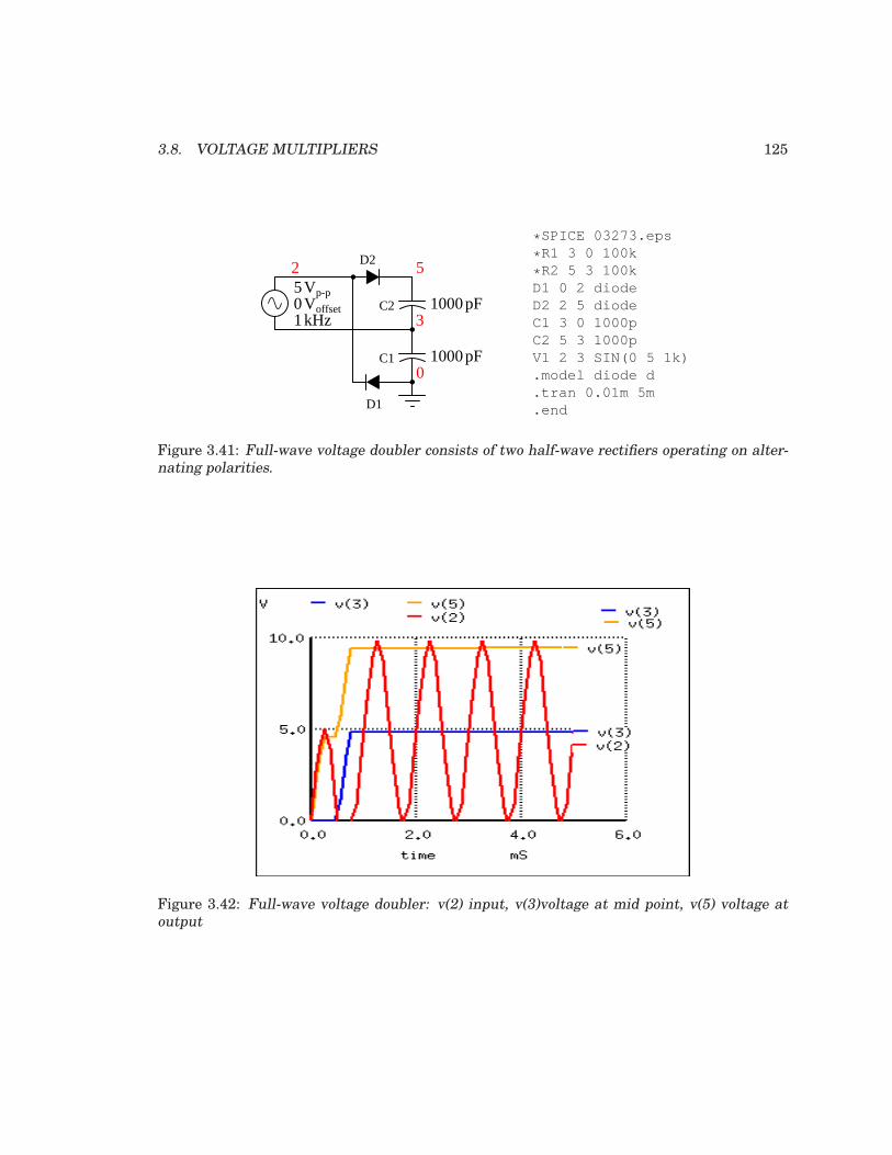
3.8. VOLTAGE MULTIPLIERS 125
5Vp-p0Voffset1kHz
1000pF
1000pF
2
3
5
0
D1
D2
C1
C2
* SPICE 03273.eps
* R1 3 0 100k
* R2 5 3 100kD1 0 2 diodeD2 2 5 diodeC1 3 0 1000pC2 5 3 1000pV1 2 3 SIN(0 5 1k).model diode d.tran 0.01m 5m.end
Figure 3.41: Full-wave voltage doubler consists of two half-wave rectifiers operating on alter-nating polarities.
Figure 3.42: Full-wave voltage doubler: v(2) input, v(3)voltage at mid point, v(5) voltage atoutput
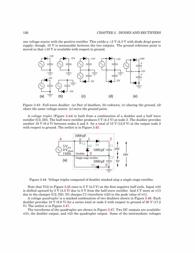
126 CHAPTER 3. DIODES AND RECTIFIERS
one voltage source with the positive rectifier. This yields a ±5 V (4.3 V with diode drop) powersupply; though, 10 V is measurable between the two outputs. The ground reference point ismoved so that +10 V is available with respect to ground.
+5V
-5V
+
+
-
-
+5V +5V +5V
-5V
-5V -5V
+5V
+10V
(a) (b) (c) (d) (e)
Figure 3.43: Full-wave doubler: (a) Pair of doublers, (b) redrawn, (c) sharing the ground, (d)share the same voltage source. (e) move the ground point.
A voltage tripler (Figure 3.44) is built from a combination of a doubler and a half waverectifier (C3, D3). The half-wave rectifier produces 5 V (4.3 V) at node 3. The doubler providesanother 10 V (8.4 V) between nodes 2 and 3. for a total of 15 V (12.9 V) at the output node 2with respect to ground. The netlist is in Figure 3.45.
5Vp-p0Voffset1kHz 3
4 1
(a)
1000pF
1000pF
2
C1D1C2D2
1000pF0D3
C3
Doubler
Single stage rectifier
10V
5V
15V
Figure 3.44: Voltage tripler composed of doubler stacked atop a single stage rectifier.
Note that V(3) in Figure 3.45 rises to 5 V (4.3 V) on the first negative half cycle. Input v(4)is shifted upward by 5 V (4.3 V) due to 5 V from the half-wave rectifier. And 5 V more at v(1)due to the clamper (C2, D2). D1 charges C1 (waveform v(2)) to the peak value of v(1).
A voltage quadrupler is a stacked combination of two doublers shown in Figure 3.46. Eachdoubler provides 10 V (8.6 V) for a series total at node 2 with respect to ground of 20 V (17.2V). The netlist is in Figure 3.47.
The waveforms of the quadrupler are shown in Figure 3.47. Two DC outputs are available:v(3), the doubler output, and v(2) the quadrupler output. Some of the intermediate voltages
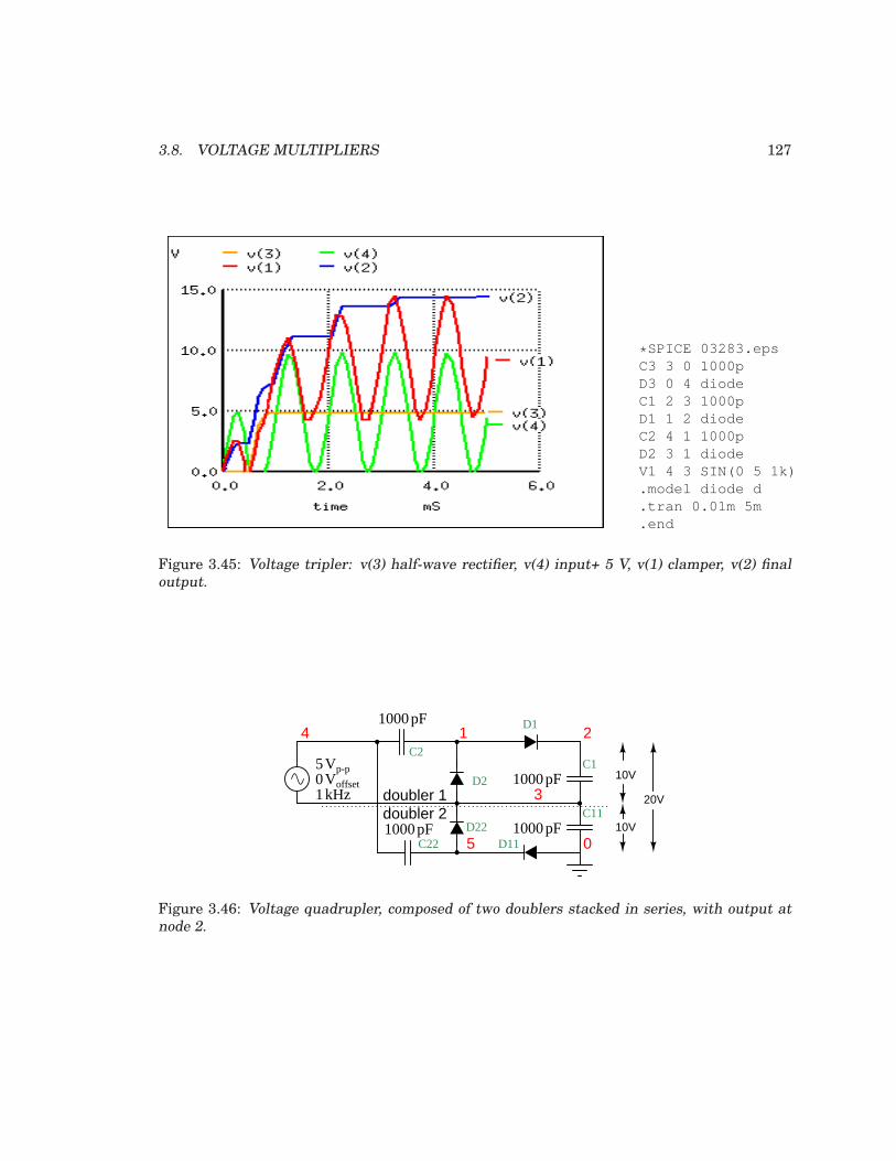
3.8. VOLTAGE MULTIPLIERS 127
* SPICE 03283.epsC3 3 0 1000pD3 0 4 diodeC1 2 3 1000pD1 1 2 diodeC2 4 1 1000pD2 3 1 diodeV1 4 3 SIN(0 5 1k).model diode d.tran 0.01m 5m.end
Figure 3.45: Voltage tripler: v(3) half-wave rectifier, v(4) input+ 5 V, v(1) clamper, v(2) finaloutput.
5Vp-p0Voffset1kHz
0
4 11000pF
1000pF
2
C1
D1
C2
D2
1000pF1000pFC22
D22D11
C11
3
5
doubler 1doubler 2
10V
10V
20V
Figure 3.46: Voltage quadrupler, composed of two doublers stacked in series, with output atnode 2.
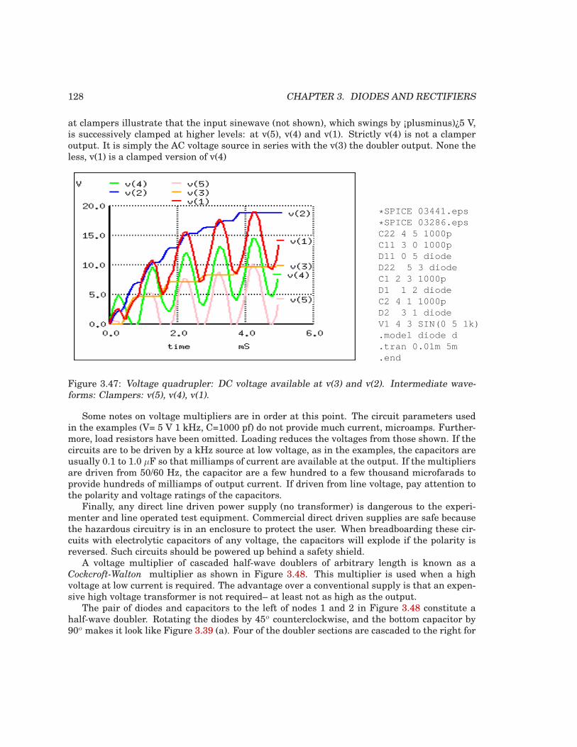
128 CHAPTER 3. DIODES AND RECTIFIERS
at clampers illustrate that the input sinewave (not shown), which swings by ¡plusminus)¿5 V,is successively clamped at higher levels: at v(5), v(4) and v(1). Strictly v(4) is not a clamperoutput. It is simply the AC voltage source in series with the v(3) the doubler output. None theless, v(1) is a clamped version of v(4)
* SPICE 03441.eps
* SPICE 03286.epsC22 4 5 1000pC11 3 0 1000pD11 0 5 diodeD22 5 3 diodeC1 2 3 1000pD1 1 2 diodeC2 4 1 1000pD2 3 1 diodeV1 4 3 SIN(0 5 1k).model diode d.tran 0.01m 5m.end
Figure 3.47: Voltage quadrupler: DC voltage available at v(3) and v(2). Intermediate wave-forms: Clampers: v(5), v(4), v(1).
Some notes on voltage multipliers are in order at this point. The circuit parameters usedin the examples (V= 5 V 1 kHz, C=1000 pf) do not provide much current, microamps. Further-more, load resistors have been omitted. Loading reduces the voltages from those shown. If thecircuits are to be driven by a kHz source at low voltage, as in the examples, the capacitors areusually 0.1 to 1.0 µF so that milliamps of current are available at the output. If the multipliersare driven from 50/60 Hz, the capacitor are a few hundred to a few thousand microfarads toprovide hundreds of milliamps of output current. If driven from line voltage, pay attention tothe polarity and voltage ratings of the capacitors.
Finally, any direct line driven power supply (no transformer) is dangerous to the experi-menter and line operated test equipment. Commercial direct driven supplies are safe becausethe hazardous circuitry is in an enclosure to protect the user. When breadboarding these cir-cuits with electrolytic capacitors of any voltage, the capacitors will explode if the polarity isreversed. Such circuits should be powered up behind a safety shield.
A voltage multiplier of cascaded half-wave doublers of arbitrary length is known as aCockcroft-Walton multiplier as shown in Figure 3.48. This multiplier is used when a highvoltage at low current is required. The advantage over a conventional supply is that an expen-sive high voltage transformer is not required– at least not as high as the output.
The pair of diodes and capacitors to the left of nodes 1 and 2 in Figure 3.48 constitute ahalf-wave doubler. Rotating the diodes by 45o counterclockwise, and the bottom capacitor by90o makes it look like Figure 3.39 (a). Four of the doubler sections are cascaded to the right for
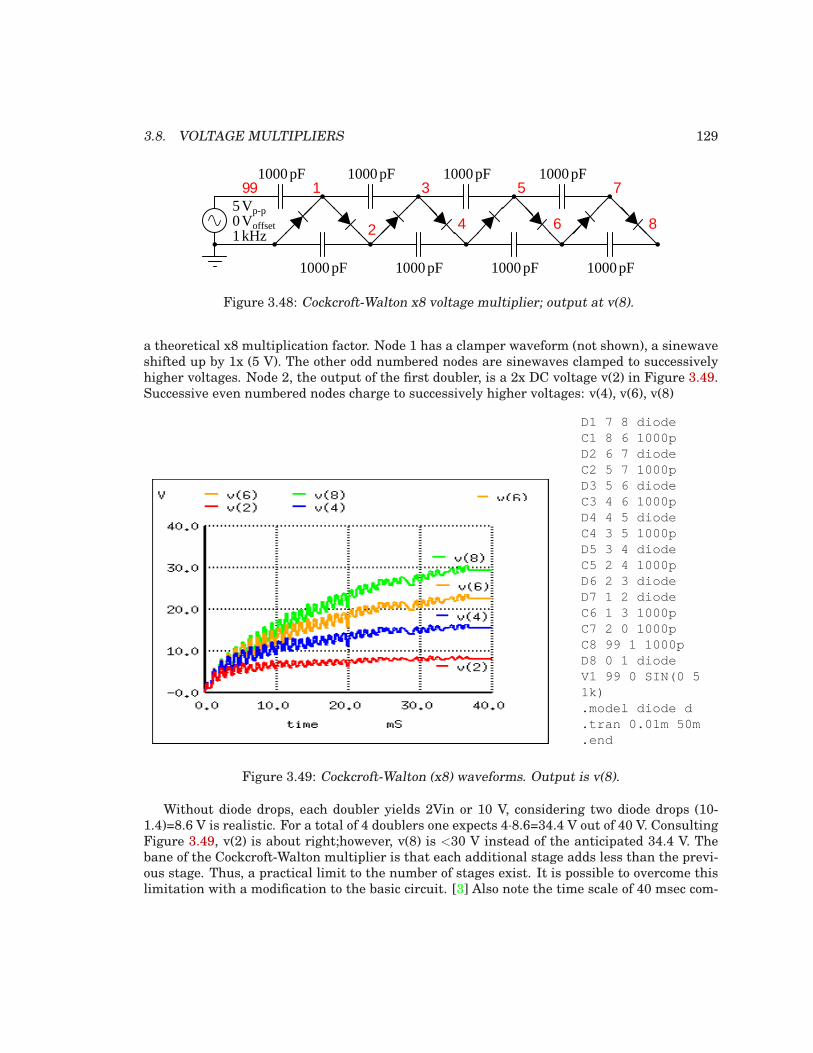
3.8. VOLTAGE MULTIPLIERS 129
5Vp-p0Voffset1kHz
1000pF 1000pF99
2
1 3
1000pF
1000pF
1000pF
1000pF
1000pF
5 7
4 6 8
1000pF
Figure 3.48: Cockcroft-Walton x8 voltage multiplier; output at v(8).
a theoretical x8 multiplication factor. Node 1 has a clamper waveform (not shown), a sinewaveshifted up by 1x (5 V). The other odd numbered nodes are sinewaves clamped to successivelyhigher voltages. Node 2, the output of the first doubler, is a 2x DC voltage v(2) in Figure 3.49.Successive even numbered nodes charge to successively higher voltages: v(4), v(6), v(8)
D1 7 8 diodeC1 8 6 1000pD2 6 7 diodeC2 5 7 1000pD3 5 6 diodeC3 4 6 1000pD4 4 5 diodeC4 3 5 1000pD5 3 4 diodeC5 2 4 1000pD6 2 3 diodeD7 1 2 diodeC6 1 3 1000pC7 2 0 1000pC8 99 1 1000pD8 0 1 diodeV1 99 0 SIN(0 51k).model diode d.tran 0.01m 50m.end
Figure 3.49: Cockcroft-Walton (x8) waveforms. Output is v(8).
Without diode drops, each doubler yields 2Vin or 10 V, considering two diode drops (10-1.4)=8.6 V is realistic. For a total of 4 doublers one expects 4·8.6=34.4 V out of 40 V. ConsultingFigure 3.49, v(2) is about right;however, v(8) is <30 V instead of the anticipated 34.4 V. Thebane of the Cockcroft-Walton multiplier is that each additional stage adds less than the previ-ous stage. Thus, a practical limit to the number of stages exist. It is possible to overcome thislimitation with a modification to the basic circuit. [3] Also note the time scale of 40 msec com-
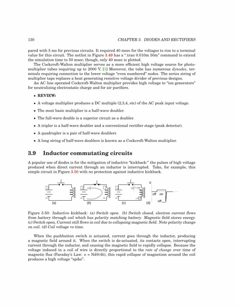
130 CHAPTER 3. DIODES AND RECTIFIERS
pared with 5 ms for previous circuits. It required 40 msec for the voltages to rise to a terminalvalue for this circuit. The netlist in Figure 3.49 has a “.tran 0.010m 50m” command to extendthe simulation time to 50 msec; though, only 40 msec is plotted.
The Cockcroft-Walton multiplier serves as a more efficient high voltage source for photo-multiplier tubes requiring up to 2000 V. [3] Moreover, the tube has numerous dynodes, ter-minals requiring connection to the lower voltage “even numbered” nodes. The series string ofmultiplier taps replaces a heat generating resistive voltage divider of previous designs.
An AC line operated Cockcroft-Walton multiplier provides high voltage to “ion generators”for neutralizing electrostatic charge and for air purifiers.
• REVIEW:
• A voltage multiplier produces a DC multiple (2,3,4, etc) of the AC peak input voltage.
• The most basic multiplier is a half-wave doubler.
• The full-wave double is a superior circuit as a doubler.
• A tripler is a half-wave doubler and a conventional rectifier stage (peak detector).
• A quadrupler is a pair of half-wave doublers
• A long string of half-wave doublers is known as a Cockcroft-Walton multiplier.
3.9 Inductor commutating circuits
A popular use of diodes is for the mitigation of inductive “kickback:” the pulses of high voltageproduced when direct current through an inductor is interrupted. Take, for example, thissimple circuit in Figure 3.50 with no protection against inductive kickback.
+
−
+
−
−+
−
+
− +
V
onoff
off(a) (b) (c) (d)
Figure 3.50: Inductive kickback: (a) Switch open. (b) Switch closed, electron current flowsfrom battery through coil which has polarity matching battery. Magnetic field stores energy.(c) Switch open, Current still flows in coil due to collapsing magnetic field. Note polarity changeon coil. (d) Coil voltage vs time.
When the pushbutton switch is actuated, current goes through the inductor, producinga magnetic field around it. When the switch is de-actuated, its contacts open, interruptingcurrent through the inductor, and causing the magnetic field to rapidly collapse. Because thevoltage induced in a coil of wire is directly proportional to the rate of change over time ofmagnetic flux (Faraday’s Law: e = NdΦ/dt), this rapid collapse of magnetism around the coilproduces a high voltage “spike”.
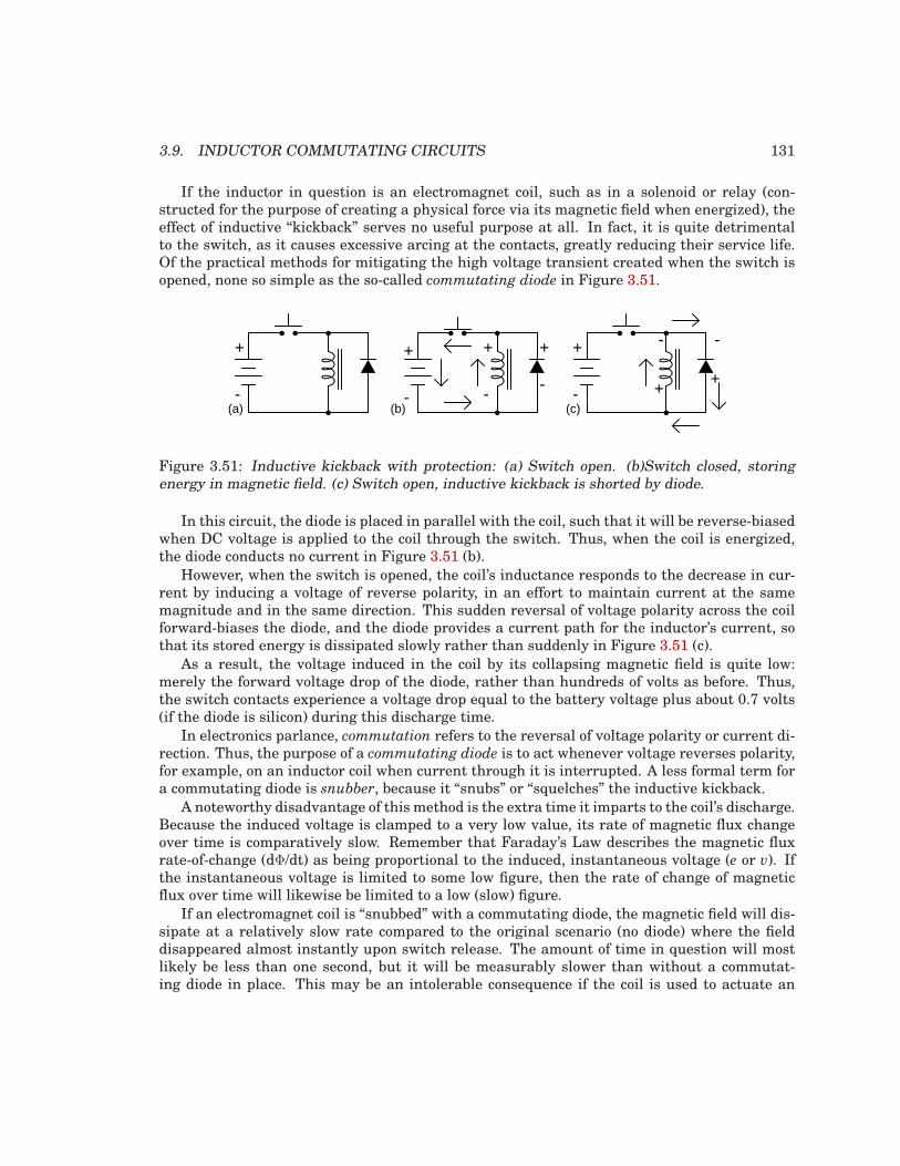
3.9. INDUCTOR COMMUTATING CIRCUITS 131
If the inductor in question is an electromagnet coil, such as in a solenoid or relay (con-structed for the purpose of creating a physical force via its magnetic field when energized), theeffect of inductive “kickback” serves no useful purpose at all. In fact, it is quite detrimentalto the switch, as it causes excessive arcing at the contacts, greatly reducing their service life.Of the practical methods for mitigating the high voltage transient created when the switch isopened, none so simple as the so-called commutating diode in Figure 3.51.
+
-
+
-
+
-
+
- +
-
+
-
(a) (b) (c)
+
-
Figure 3.51: Inductive kickback with protection: (a) Switch open. (b)Switch closed, storingenergy in magnetic field. (c) Switch open, inductive kickback is shorted by diode.
In this circuit, the diode is placed in parallel with the coil, such that it will be reverse-biasedwhen DC voltage is applied to the coil through the switch. Thus, when the coil is energized,the diode conducts no current in Figure 3.51 (b).
However, when the switch is opened, the coil’s inductance responds to the decrease in cur-rent by inducing a voltage of reverse polarity, in an effort to maintain current at the samemagnitude and in the same direction. This sudden reversal of voltage polarity across the coilforward-biases the diode, and the diode provides a current path for the inductor’s current, sothat its stored energy is dissipated slowly rather than suddenly in Figure 3.51 (c).
As a result, the voltage induced in the coil by its collapsing magnetic field is quite low:merely the forward voltage drop of the diode, rather than hundreds of volts as before. Thus,the switch contacts experience a voltage drop equal to the battery voltage plus about 0.7 volts(if the diode is silicon) during this discharge time.
In electronics parlance, commutation refers to the reversal of voltage polarity or current di-rection. Thus, the purpose of a commutating diode is to act whenever voltage reverses polarity,for example, on an inductor coil when current through it is interrupted. A less formal term fora commutating diode is snubber, because it “snubs” or “squelches” the inductive kickback.
A noteworthy disadvantage of this method is the extra time it imparts to the coil’s discharge.Because the induced voltage is clamped to a very low value, its rate of magnetic flux changeover time is comparatively slow. Remember that Faraday’s Law describes the magnetic fluxrate-of-change (dΦ/dt) as being proportional to the induced, instantaneous voltage (e or v). Ifthe instantaneous voltage is limited to some low figure, then the rate of change of magneticflux over time will likewise be limited to a low (slow) figure.
If an electromagnet coil is “snubbed” with a commutating diode, the magnetic field will dis-sipate at a relatively slow rate compared to the original scenario (no diode) where the fielddisappeared almost instantly upon switch release. The amount of time in question will mostlikely be less than one second, but it will be measurably slower than without a commutat-ing diode in place. This may be an intolerable consequence if the coil is used to actuate an
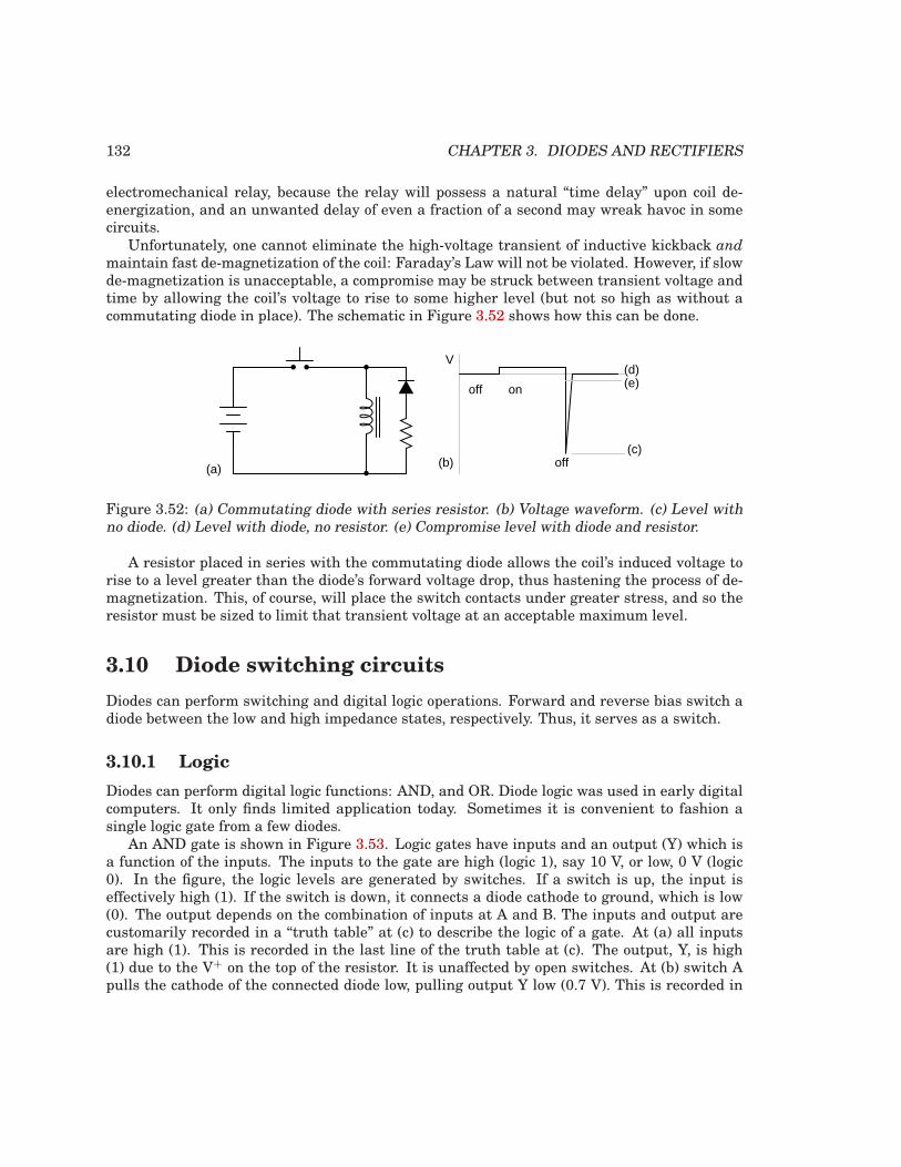
132 CHAPTER 3. DIODES AND RECTIFIERS
electromechanical relay, because the relay will possess a natural “time delay” upon coil de-energization, and an unwanted delay of even a fraction of a second may wreak havoc in somecircuits.
Unfortunately, one cannot eliminate the high-voltage transient of inductive kickback and
maintain fast de-magnetization of the coil: Faraday’s Law will not be violated. However, if slowde-magnetization is unacceptable, a compromise may be struck between transient voltage andtime by allowing the coil’s voltage to rise to some higher level (but not so high as without acommutating diode in place). The schematic in Figure 3.52 shows how this can be done.
off
off
on
(a) (b)
(e)
V(d)
(c)
Figure 3.52: (a) Commutating diode with series resistor. (b) Voltage waveform. (c) Level withno diode. (d) Level with diode, no resistor. (e) Compromise level with diode and resistor.
A resistor placed in series with the commutating diode allows the coil’s induced voltage torise to a level greater than the diode’s forward voltage drop, thus hastening the process of de-magnetization. This, of course, will place the switch contacts under greater stress, and so theresistor must be sized to limit that transient voltage at an acceptable maximum level.
3.10 Diode switching circuits
Diodes can perform switching and digital logic operations. Forward and reverse bias switch adiode between the low and high impedance states, respectively. Thus, it serves as a switch.
3.10.1 Logic
Diodes can perform digital logic functions: AND, and OR. Diode logic was used in early digitalcomputers. It only finds limited application today. Sometimes it is convenient to fashion asingle logic gate from a few diodes.
An AND gate is shown in Figure 3.53. Logic gates have inputs and an output (Y) which isa function of the inputs. The inputs to the gate are high (logic 1), say 10 V, or low, 0 V (logic0). In the figure, the logic levels are generated by switches. If a switch is up, the input iseffectively high (1). If the switch is down, it connects a diode cathode to ground, which is low(0). The output depends on the combination of inputs at A and B. The inputs and output arecustomarily recorded in a “truth table” at (c) to describe the logic of a gate. At (a) all inputsare high (1). This is recorded in the last line of the truth table at (c). The output, Y, is high(1) due to the V+ on the top of the resistor. It is unaffected by open switches. At (b) switch Apulls the cathode of the connected diode low, pulling output Y low (0.7 V). This is recorded in
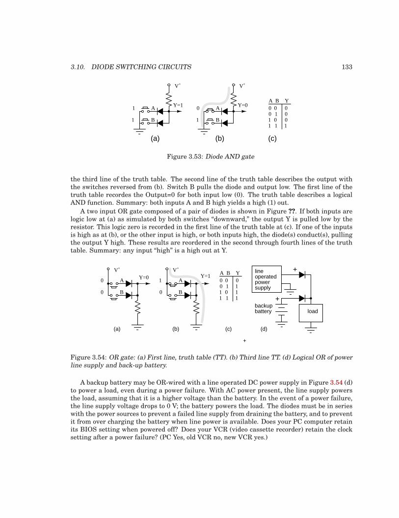
3.10. DIODE SWITCHING CIRCUITS 133
V+
A
B
V+
A
B
Y=1 Y=0 0 0 00 1 01 0 01 1 1
A B Y0
1
1
1
(a) (b) (c)
Figure 3.53: Diode AND gate
the third line of the truth table. The second line of the truth table describes the output withthe switches reversed from (b). Switch B pulls the diode and output low. The first line of thetruth table recordes the Output=0 for both input low (0). The truth table describes a logicalAND function. Summary: both inputs A and B high yields a high (1) out.
A two input OR gate composed of a pair of diodes is shown in Figure ??. If both inputs arelogic low at (a) as simulated by both switches “downward,” the output Y is pulled low by theresistor. This logic zero is recorded in the first line of the truth table at (c). If one of the inputsis high as at (b), or the other input is high, or both inputs high, the diode(s) conduct(s), pullingthe output Y high. These results are reordered in the second through fourth lines of the truthtable. Summary: any input “high” is a high out at Y.
A
B
Y=10 0 00 11 01 1 1
A B Y
0
1
(a) (b) (c)
11
V+
A
B
Y=0
0
V+
0
load
lineoperatedpowersupply
backupbattery
(d)
+
+
+
Figure 3.54: OR gate: (a) First line, truth table (TT). (b) Third line TT. (d) Logical OR of powerline supply and back-up battery.
A backup battery may be OR-wired with a line operated DC power supply in Figure 3.54 (d)to power a load, even during a power failure. With AC power present, the line supply powersthe load, assuming that it is a higher voltage than the battery. In the event of a power failure,the line supply voltage drops to 0 V; the battery powers the load. The diodes must be in serieswith the power sources to prevent a failed line supply from draining the battery, and to preventit from over charging the battery when line power is available. Does your PC computer retainits BIOS setting when powered off? Does your VCR (video cassette recorder) retain the clocksetting after a power failure? (PC Yes, old VCR no, new VCR yes.)
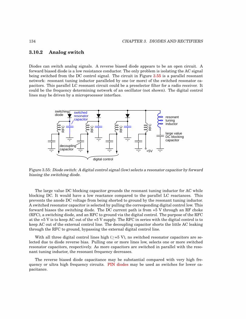
134 CHAPTER 3. DIODES AND RECTIFIERS
3.10.2 Analog switch
Diodes can switch analog signals. A reverse biased diode appears to be an open circuit. Aforward biased diode is a low resistance conductor. The only problem is isolating the AC signalbeing switched from the DC control signal. The circuit in Figure 3.55 is a parallel resonantnetwork: resonant tuning inductor paralleled by one (or more) of the switched resonator ca-pacitors. This parallel LC resonant circuit could be a preselector filter for a radio receiver. Itcould be the frequency determining network of an oscillator (not shown). The digital controllines may be driven by a microprocessor interface.
+5V
RF
C
RF
C
RF
C
RF
C
digital control
large valueDC blocking capacitor
resonant tuning inductor
switched resonator capacitor
decoupling capacitor
switching diode
Figure 3.55: Diode switch: A digital control signal (low) selects a resonator capacitor by forwardbiasing the switching diode.
The large value DC blocking capacitor grounds the resonant tuning inductor for AC whileblocking DC. It would have a low reactance compared to the parallel LC reactances. Thisprevents the anode DC voltage from being shorted to ground by the resonant tuning inductor.A switched resonator capacitor is selected by pulling the corresponding digital control low. Thisforward biases the switching diode. The DC current path is from +5 V through an RF choke(RFC), a switching diode, and an RFC to ground via the digital control. The purpose of the RFCat the +5 V is to keep AC out of the +5 V supply. The RFC in series with the digital control is tokeep AC out of the external control line. The decoupling capacitor shorts the little AC leakingthrough the RFC to ground, bypassing the external digital control line.
With all three digital control lines high (≥+5 V), no switched resonator capacitors are se-lected due to diode reverse bias. Pulling one or more lines low, selects one or more switchedresonator capacitors, respectively. As more capacitors are switched in parallel with the reso-nant tuning inductor, the resonant frequency decreases.
The reverse biased diode capacitance may be substantial compared with very high fre-quency or ultra high frequency circuits. PIN diodes may be used as switches for lower ca-pacitance.
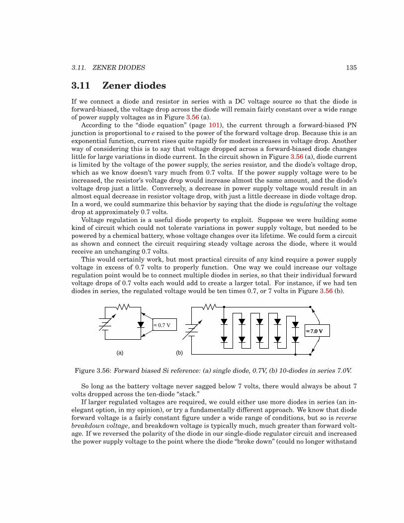
3.11. ZENER DIODES 135
3.11 Zener diodes
If we connect a diode and resistor in series with a DC voltage source so that the diode isforward-biased, the voltage drop across the diode will remain fairly constant over a wide rangeof power supply voltages as in Figure 3.56 (a).
According to the “diode equation” (page 101), the current through a forward-biased PNjunction is proportional to e raised to the power of the forward voltage drop. Because this is anexponential function, current rises quite rapidly for modest increases in voltage drop. Anotherway of considering this is to say that voltage dropped across a forward-biased diode changeslittle for large variations in diode current. In the circuit shown in Figure 3.56 (a), diode currentis limited by the voltage of the power supply, the series resistor, and the diode’s voltage drop,which as we know doesn’t vary much from 0.7 volts. If the power supply voltage were to beincreased, the resistor’s voltage drop would increase almost the same amount, and the diode’svoltage drop just a little. Conversely, a decrease in power supply voltage would result in analmost equal decrease in resistor voltage drop, with just a little decrease in diode voltage drop.In a word, we could summarize this behavior by saying that the diode is regulating the voltagedrop at approximately 0.7 volts.
Voltage regulation is a useful diode property to exploit. Suppose we were building somekind of circuit which could not tolerate variations in power supply voltage, but needed to bepowered by a chemical battery, whose voltage changes over its lifetime. We could form a circuitas shown and connect the circuit requiring steady voltage across the diode, where it wouldreceive an unchanging 0.7 volts.
This would certainly work, but most practical circuits of any kind require a power supplyvoltage in excess of 0.7 volts to properly function. One way we could increase our voltageregulation point would be to connect multiple diodes in series, so that their individual forwardvoltage drops of 0.7 volts each would add to create a larger total. For instance, if we had tendiodes in series, the regulated voltage would be ten times 0.7, or 7 volts in Figure 3.56 (b).
≈ 7.0 V≈ 0.7 V
≈7.0 V
(a) (b)
Figure 3.56: Forward biased Si reference: (a) single diode, 0.7V, (b) 10-diodes in series 7.0V.
So long as the battery voltage never sagged below 7 volts, there would always be about 7volts dropped across the ten-diode “stack.”
If larger regulated voltages are required, we could either use more diodes in series (an in-elegant option, in my opinion), or try a fundamentally different approach. We know that diodeforward voltage is a fairly constant figure under a wide range of conditions, but so is reverse
breakdown voltage, and breakdown voltage is typically much, much greater than forward volt-age. If we reversed the polarity of the diode in our single-diode regulator circuit and increasedthe power supply voltage to the point where the diode “broke down” (could no longer withstand
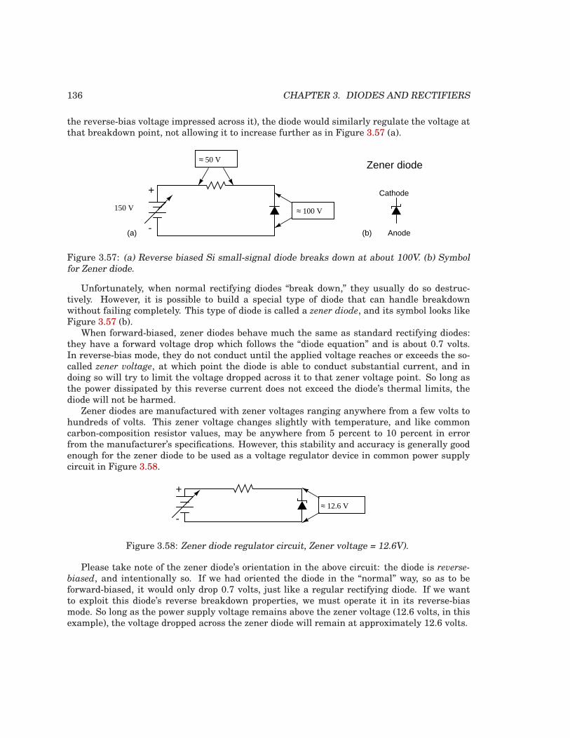
136 CHAPTER 3. DIODES AND RECTIFIERS
the reverse-bias voltage impressed across it), the diode would similarly regulate the voltage atthat breakdown point, not allowing it to increase further as in Figure 3.57 (a).
150 V ≈ 100 V
≈ 50 VZener diode
Anode
Cathode
(a) (b)
+
-
Figure 3.57: (a) Reverse biased Si small-signal diode breaks down at about 100V. (b) Symbolfor Zener diode.
Unfortunately, when normal rectifying diodes “break down,” they usually do so destruc-tively. However, it is possible to build a special type of diode that can handle breakdownwithout failing completely. This type of diode is called a zener diode, and its symbol looks likeFigure 3.57 (b).
When forward-biased, zener diodes behave much the same as standard rectifying diodes:they have a forward voltage drop which follows the “diode equation” and is about 0.7 volts.In reverse-bias mode, they do not conduct until the applied voltage reaches or exceeds the so-called zener voltage, at which point the diode is able to conduct substantial current, and indoing so will try to limit the voltage dropped across it to that zener voltage point. So long asthe power dissipated by this reverse current does not exceed the diode’s thermal limits, thediode will not be harmed.
Zener diodes are manufactured with zener voltages ranging anywhere from a few volts tohundreds of volts. This zener voltage changes slightly with temperature, and like commoncarbon-composition resistor values, may be anywhere from 5 percent to 10 percent in errorfrom the manufacturer’s specifications. However, this stability and accuracy is generally goodenough for the zener diode to be used as a voltage regulator device in common power supplycircuit in Figure 3.58.
≈ 12.6 V
+
-
Figure 3.58: Zener diode regulator circuit, Zener voltage = 12.6V).
Please take note of the zener diode’s orientation in the above circuit: the diode is reverse-
biased, and intentionally so. If we had oriented the diode in the “normal” way, so as to beforward-biased, it would only drop 0.7 volts, just like a regular rectifying diode. If we wantto exploit this diode’s reverse breakdown properties, we must operate it in its reverse-biasmode. So long as the power supply voltage remains above the zener voltage (12.6 volts, in thisexample), the voltage dropped across the zener diode will remain at approximately 12.6 volts.
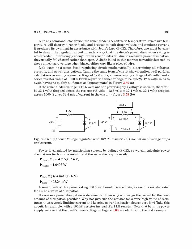
3.11. ZENER DIODES 137
Like any semiconductor device, the zener diode is sensitive to temperature. Excessive tem-perature will destroy a zener diode, and because it both drops voltage and conducts current,it produces its own heat in accordance with Joule’s Law (P=IE). Therefore, one must be care-ful to design the regulator circuit in such a way that the diode’s power dissipation rating isnot exceeded. Interestingly enough, when zener diodes fail due to excessive power dissipation,they usually fail shorted rather than open. A diode failed in this manner is readily detected: itdrops almost zero voltage when biased either way, like a piece of wire.
Let’s examine a zener diode regulating circuit mathematically, determining all voltages,currents, and power dissipations. Taking the same form of circuit shown earlier, we’ll performcalculations assuming a zener voltage of 12.6 volts, a power supply voltage of 45 volts, and aseries resistor value of 1000 Ω (we’ll regard the zener voltage to be exactly 12.6 volts so as toavoid having to qualify all figures as “approximate” in Figure 3.59 (a)
If the zener diode’s voltage is 12.6 volts and the power supply’s voltage is 45 volts, there willbe 32.4 volts dropped across the resistor (45 volts - 12.6 volts = 32.4 volts). 32.4 volts droppedacross 1000 Ω gives 32.4 mA of current in the circuit. (Figure 3.59 (b))
45 V
1 kΩ
32.4 mA
32.4 mA
32.4 V
12.6 V45 V
1 kΩ
12.6 V
+
-
+
-(a) (b)
Figure 3.59: (a) Zener Voltage regulator with 1000 Ω resistor. (b) Calculation of voltage dropsand current.
Power is calculated by multiplying current by voltage (P=IE), so we can calculate powerdissipations for both the resistor and the zener diode quite easily:
Presistor = (32.4 mA)(32.4 V)
Pdiode = (32.4 mA)(12.6 V)
Presistor = 1.0498 W
Pdiode = 408.24 mW
A zener diode with a power rating of 0.5 watt would be adequate, as would a resistor ratedfor 1.5 or 2 watts of dissipation.
If excessive power dissipation is detrimental, then why not design the circuit for the leastamount of dissipation possible? Why not just size the resistor for a very high value of resis-tance, thus severely limiting current and keeping power dissipation figures very low? Take thiscircuit, for example, with a 100 kΩ resistor instead of a 1 kΩ resistor. Note that both the powersupply voltage and the diode’s zener voltage in Figure 3.60 are identical to the last example:
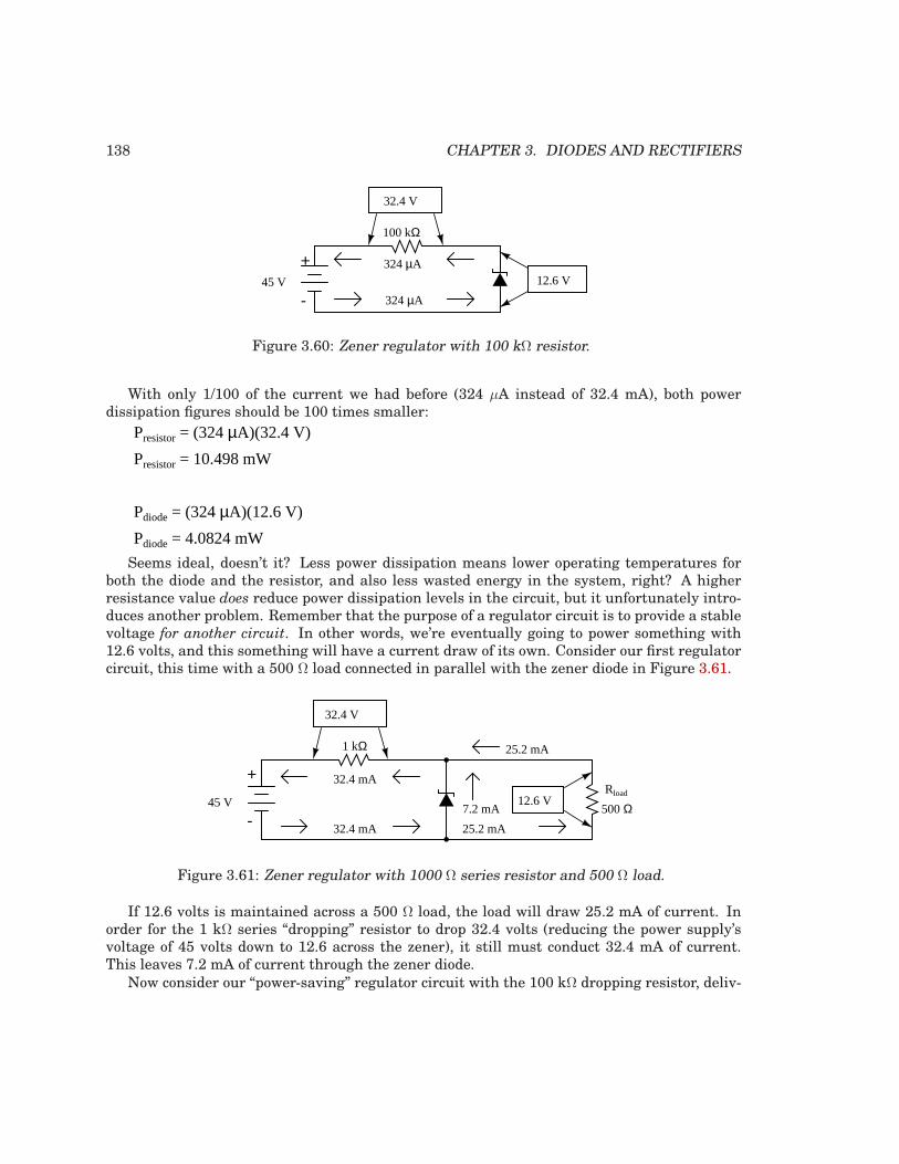
138 CHAPTER 3. DIODES AND RECTIFIERS
45 V
32.4 V
12.6 V
100 kΩ
324 µA
324 µA+
-
Figure 3.60: Zener regulator with 100 kΩ resistor.
With only 1/100 of the current we had before (324 µA instead of 32.4 mA), both powerdissipation figures should be 100 times smaller:
Presistor = (324 µA)(32.4 V)
Presistor = 10.498 mW
Pdiode = (324 µA)(12.6 V)
Pdiode = 4.0824 mW
Seems ideal, doesn’t it? Less power dissipation means lower operating temperatures forboth the diode and the resistor, and also less wasted energy in the system, right? A higherresistance value does reduce power dissipation levels in the circuit, but it unfortunately intro-duces another problem. Remember that the purpose of a regulator circuit is to provide a stablevoltage for another circuit. In other words, we’re eventually going to power something with12.6 volts, and this something will have a current draw of its own. Consider our first regulatorcircuit, this time with a 500 Ω load connected in parallel with the zener diode in Figure 3.61.
45 V
1 kΩ
32.4 mA
32.4 mA
32.4 V
12.6 VRload
500 Ω25.2 mA
25.2 mA
7.2 mA
+
-
Figure 3.61: Zener regulator with 1000 Ω series resistor and 500 Ω load.
If 12.6 volts is maintained across a 500 Ω load, the load will draw 25.2 mA of current. Inorder for the 1 kΩ series “dropping” resistor to drop 32.4 volts (reducing the power supply’svoltage of 45 volts down to 12.6 across the zener), it still must conduct 32.4 mA of current.This leaves 7.2 mA of current through the zener diode.
Now consider our “power-saving” regulator circuit with the 100 kΩ dropping resistor, deliv-
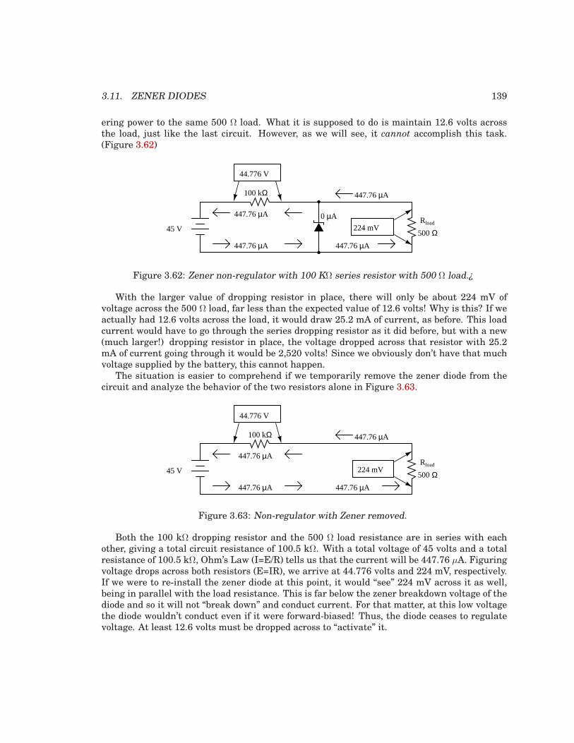
3.11. ZENER DIODES 139
ering power to the same 500 Ω load. What it is supposed to do is maintain 12.6 volts acrossthe load, just like the last circuit. However, as we will see, it cannot accomplish this task.(Figure 3.62)
45 VRload
500 Ω
100 kΩ
224 mV
44.776 V
447.76 µA
447.76 µA 447.76 µA
447.76 µA
0 µA
Figure 3.62: Zener non-regulator with 100 KΩ series resistor with 500 Ω load.¿
With the larger value of dropping resistor in place, there will only be about 224 mV ofvoltage across the 500 Ω load, far less than the expected value of 12.6 volts! Why is this? If weactually had 12.6 volts across the load, it would draw 25.2 mA of current, as before. This loadcurrent would have to go through the series dropping resistor as it did before, but with a new(much larger!) dropping resistor in place, the voltage dropped across that resistor with 25.2mA of current going through it would be 2,520 volts! Since we obviously don’t have that muchvoltage supplied by the battery, this cannot happen.
The situation is easier to comprehend if we temporarily remove the zener diode from thecircuit and analyze the behavior of the two resistors alone in Figure 3.63.
45 VRload
500 Ω
100 kΩ
224 mV
44.776 V
447.76 µA
447.76 µA 447.76 µA
447.76 µA
Figure 3.63: Non-regulator with Zener removed.
Both the 100 kΩ dropping resistor and the 500 Ω load resistance are in series with eachother, giving a total circuit resistance of 100.5 kΩ. With a total voltage of 45 volts and a totalresistance of 100.5 kΩ, Ohm’s Law (I=E/R) tells us that the current will be 447.76 µA. Figuringvoltage drops across both resistors (E=IR), we arrive at 44.776 volts and 224 mV, respectively.If we were to re-install the zener diode at this point, it would “see” 224 mV across it as well,being in parallel with the load resistance. This is far below the zener breakdown voltage of thediode and so it will not “break down” and conduct current. For that matter, at this low voltagethe diode wouldn’t conduct even if it were forward-biased! Thus, the diode ceases to regulatevoltage. At least 12.6 volts must be dropped across to “activate” it.
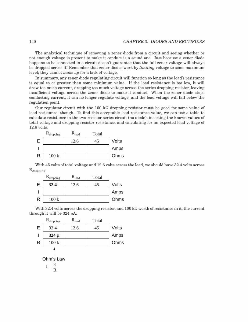
140 CHAPTER 3. DIODES AND RECTIFIERS
The analytical technique of removing a zener diode from a circuit and seeing whether ornot enough voltage is present to make it conduct is a sound one. Just because a zener diodehappens to be connected in a circuit doesn’t guarantee that the full zener voltage will alwaysbe dropped across it! Remember that zener diodes work by limiting voltage to some maximumlevel; they cannot make up for a lack of voltage.
In summary, any zener diode regulating circuit will function so long as the load’s resistanceis equal to or greater than some minimum value. If the load resistance is too low, it willdraw too much current, dropping too much voltage across the series dropping resistor, leavinginsufficient voltage across the zener diode to make it conduct. When the zener diode stopsconducting current, it can no longer regulate voltage, and the load voltage will fall below theregulation point.
Our regulator circuit with the 100 kΩ dropping resistor must be good for some value ofload resistance, though. To find this acceptable load resistance value, we can use a table tocalculate resistance in the two-resistor series circuit (no diode), inserting the known values oftotal voltage and dropping resistor resistance, and calculating for an expected load voltage of12.6 volts:
E
I
R
Volts
Amps
Ohms
Rdropping Rload Total
100 k
4512.6
With 45 volts of total voltage and 12.6 volts across the load, we should have 32.4 volts acrossRdropping:
E
I
R
Volts
Amps
Ohms
Rdropping Rload Total
100 k
4512.632.4
With 32.4 volts across the dropping resistor, and 100 kΩ worth of resistance in it, the currentthrough it will be 324 µA:
E
I
R
Volts
Amps
Ohms
Rdropping Rload Total
100 k
4512.632.4
324 µ
Ohm’s Law
I = ER
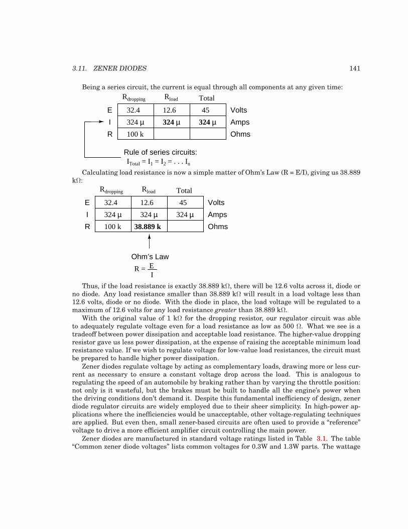
3.11. ZENER DIODES 141
Being a series circuit, the current is equal through all components at any given time:
E
I
R
Volts
Amps
Ohms
Rdropping Rload Total
100 k
4512.632.4
324 µ 324 µ 324 µ
Rule of series circuits:ITotal = I1 = I2 = . . . In
Calculating load resistance is now a simple matter of Ohm’s Law (R = E/I), giving us 38.889kΩ:
E
I
R
Volts
Amps
Ohms
Rdropping Rload Total
100 k
4512.632.4
324 µ 324 µ 324 µ38.889 k
Ohm’s Law
R = EI
Thus, if the load resistance is exactly 38.889 kΩ, there will be 12.6 volts across it, diode orno diode. Any load resistance smaller than 38.889 kΩ will result in a load voltage less than12.6 volts, diode or no diode. With the diode in place, the load voltage will be regulated to amaximum of 12.6 volts for any load resistance greater than 38.889 kΩ.
With the original value of 1 kΩ for the dropping resistor, our regulator circuit was ableto adequately regulate voltage even for a load resistance as low as 500 Ω. What we see is atradeoff between power dissipation and acceptable load resistance. The higher-value droppingresistor gave us less power dissipation, at the expense of raising the acceptable minimum loadresistance value. If we wish to regulate voltage for low-value load resistances, the circuit mustbe prepared to handle higher power dissipation.
Zener diodes regulate voltage by acting as complementary loads, drawing more or less cur-rent as necessary to ensure a constant voltage drop across the load. This is analogous toregulating the speed of an automobile by braking rather than by varying the throttle position:not only is it wasteful, but the brakes must be built to handle all the engine’s power whenthe driving conditions don’t demand it. Despite this fundamental inefficiency of design, zenerdiode regulator circuits are widely employed due to their sheer simplicity. In high-power ap-plications where the inefficiencies would be unacceptable, other voltage-regulating techniquesare applied. But even then, small zener-based circuits are often used to provide a “reference”voltage to drive a more efficient amplifier circuit controlling the main power.
Zener diodes are manufactured in standard voltage ratings listed in Table 3.1. The table“Common zener diode voltages” lists common voltages for 0.3W and 1.3W parts. The wattage
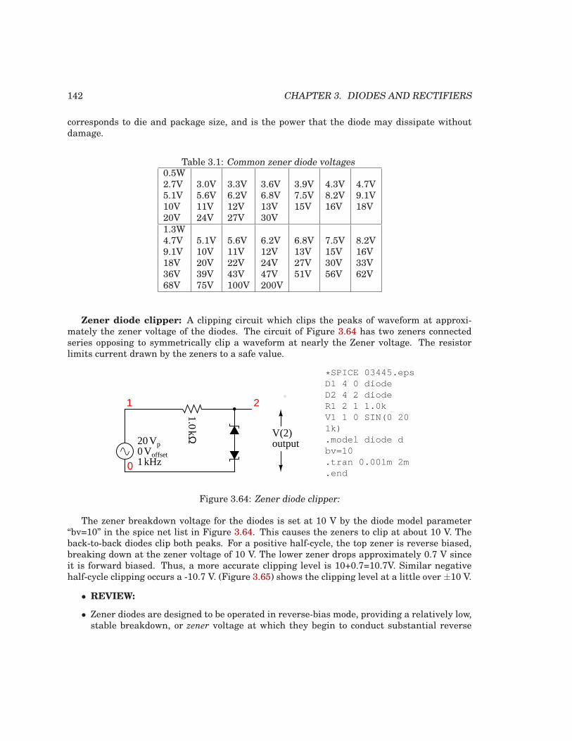
142 CHAPTER 3. DIODES AND RECTIFIERS
corresponds to die and package size, and is the power that the diode may dissipate withoutdamage.
Table 3.1: Common zener diode voltages0.5W2.7V 3.0V 3.3V 3.6V 3.9V 4.3V 4.7V5.1V 5.6V 6.2V 6.8V 7.5V 8.2V 9.1V10V 11V 12V 13V 15V 16V 18V20V 24V 27V 30V1.3W4.7V 5.1V 5.6V 6.2V 6.8V 7.5V 8.2V9.1V 10V 11V 12V 13V 15V 16V18V 20V 22V 24V 27V 30V 33V36V 39V 43V 47V 51V 56V 62V68V 75V 100V 200V
Zener diode clipper: A clipping circuit which clips the peaks of waveform at approxi-mately the zener voltage of the diodes. The circuit of Figure 3.64 has two zeners connectedseries opposing to symmetrically clip a waveform at nearly the Zener voltage. The resistorlimits current drawn by the zeners to a safe value.
20Vp0 Voffset1 kHz
1.0kΩ
0
1 2
V(2)output
* SPICE 03445.epsD1 4 0 diodeD2 4 2 diodeR1 2 1 1.0kV1 1 0 SIN(0 201k).model diode dbv=10.tran 0.001m 2m.end
Figure 3.64: Zener diode clipper:
The zener breakdown voltage for the diodes is set at 10 V by the diode model parameter“bv=10” in the spice net list in Figure 3.64. This causes the zeners to clip at about 10 V. Theback-to-back diodes clip both peaks. For a positive half-cycle, the top zener is reverse biased,breaking down at the zener voltage of 10 V. The lower zener drops approximately 0.7 V sinceit is forward biased. Thus, a more accurate clipping level is 10+0.7=10.7V. Similar negativehalf-cycle clipping occurs a -10.7 V. (Figure 3.65) shows the clipping level at a little over ±10 V.
• REVIEW:
• Zener diodes are designed to be operated in reverse-bias mode, providing a relatively low,stable breakdown, or zener voltage at which they begin to conduct substantial reverse
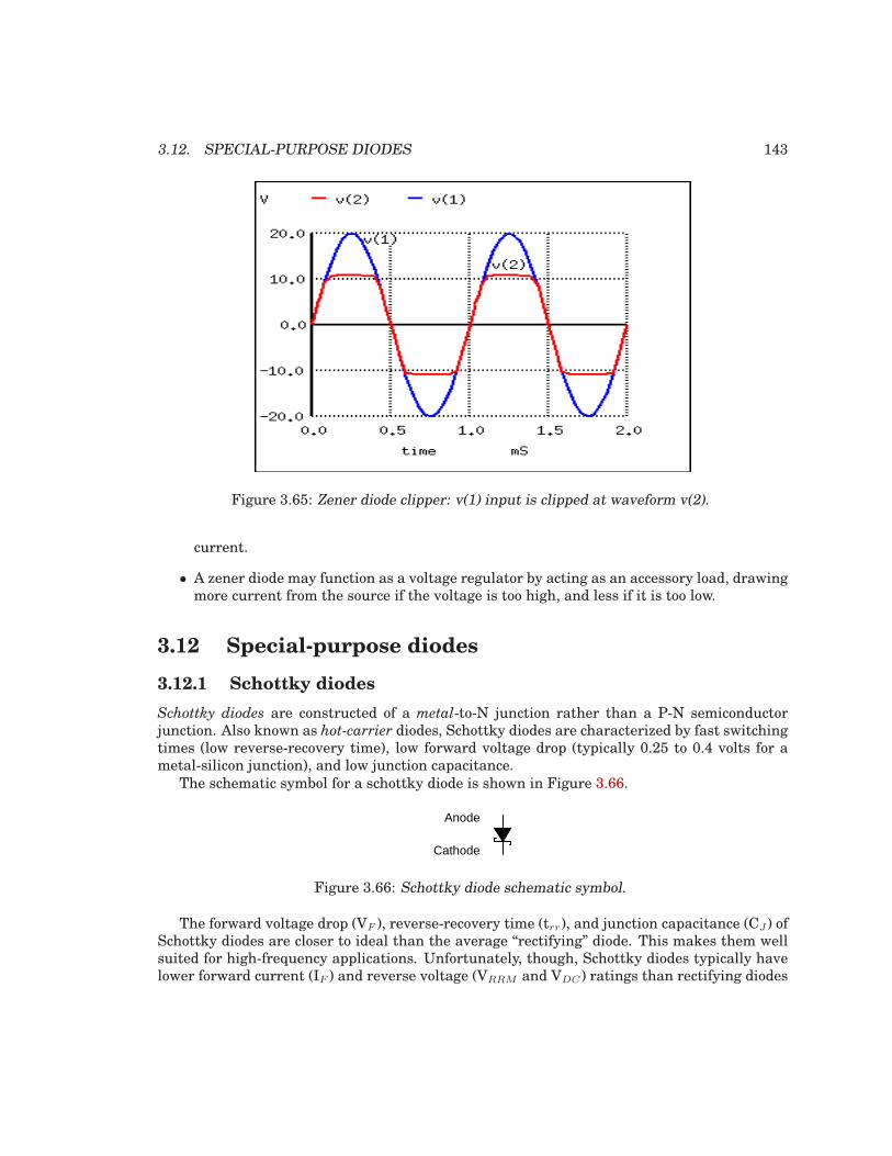
3.12. SPECIAL-PURPOSE DIODES 143
Figure 3.65: Zener diode clipper: v(1) input is clipped at waveform v(2).
current.
• A zener diode may function as a voltage regulator by acting as an accessory load, drawingmore current from the source if the voltage is too high, and less if it is too low.
3.12 Special-purpose diodes
3.12.1 Schottky diodes
Schottky diodes are constructed of a metal-to-N junction rather than a P-N semiconductorjunction. Also known as hot-carrier diodes, Schottky diodes are characterized by fast switchingtimes (low reverse-recovery time), low forward voltage drop (typically 0.25 to 0.4 volts for ametal-silicon junction), and low junction capacitance.
The schematic symbol for a schottky diode is shown in Figure 3.66.
Anode
Cathode
Figure 3.66: Schottky diode schematic symbol.
The forward voltage drop (VF ), reverse-recovery time (trr), and junction capacitance (CJ ) ofSchottky diodes are closer to ideal than the average “rectifying” diode. This makes them wellsuited for high-frequency applications. Unfortunately, though, Schottky diodes typically havelower forward current (IF ) and reverse voltage (VRRM and VDC) ratings than rectifying diodes
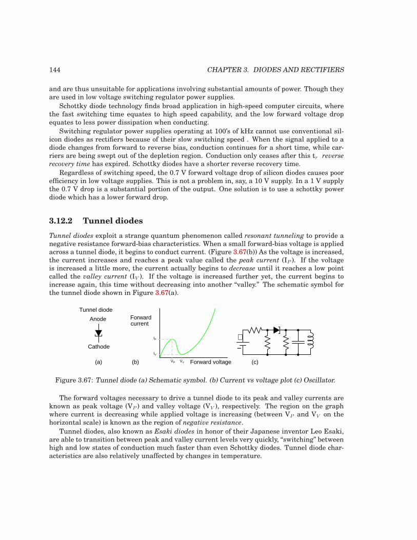
144 CHAPTER 3. DIODES AND RECTIFIERS
and are thus unsuitable for applications involving substantial amounts of power. Though theyare used in low voltage switching regulator power supplies.
Schottky diode technology finds broad application in high-speed computer circuits, wherethe fast switching time equates to high speed capability, and the low forward voltage dropequates to less power dissipation when conducting.
Switching regulator power supplies operating at 100’s of kHz cannot use conventional sil-icon diodes as rectifiers because of their slow switching speed . When the signal applied to adiode changes from forward to reverse bias, conduction continues for a short time, while car-riers are being swept out of the depletion region. Conduction only ceases after this tr reverse
recovery time has expired. Schottky diodes have a shorter reverse recovery time.
Regardless of switching speed, the 0.7 V forward voltage drop of silicon diodes causes poorefficiency in low voltage supplies. This is not a problem in, say, a 10 V supply. In a 1 V supplythe 0.7 V drop is a substantial portion of the output. One solution is to use a schottky powerdiode which has a lower forward drop.
3.12.2 Tunnel diodes
Tunnel diodes exploit a strange quantum phenomenon called resonant tunneling to provide anegative resistance forward-bias characteristics. When a small forward-bias voltage is appliedacross a tunnel diode, it begins to conduct current. (Figure 3.67(b)) As the voltage is increased,the current increases and reaches a peak value called the peak current (IP ). If the voltageis increased a little more, the current actually begins to decrease until it reaches a low pointcalled the valley current (IV ). If the voltage is increased further yet, the current begins toincrease again, this time without decreasing into another “valley.” The schematic symbol forthe tunnel diode shown in Figure 3.67(a).
Anode
Cathode
Tunnel diode
Forward voltage
Forwardcurrent
IP
IV
VP VV(a) (b) (c)
+−
Figure 3.67: Tunnel diode (a) Schematic symbol. (b) Current vs voltage plot (c) Oscillator.
The forward voltages necessary to drive a tunnel diode to its peak and valley currents areknown as peak voltage (VP ) and valley voltage (VV ), respectively. The region on the graphwhere current is decreasing while applied voltage is increasing (between VP and VV on thehorizontal scale) is known as the region of negative resistance.
Tunnel diodes, also known as Esaki diodes in honor of their Japanese inventor Leo Esaki,are able to transition between peak and valley current levels very quickly, “switching” betweenhigh and low states of conduction much faster than even Schottky diodes. Tunnel diode char-acteristics are also relatively unaffected by changes in temperature.
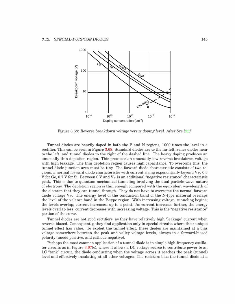
3.12. SPECIAL-PURPOSE DIODES 145
Doping concentration (cm-3)
Bre
akdo
wn
volta
ge (
V)
1014 1015 1016 1017 10181
10
100
1000
GaP
GaAsSi
Ge
tunneling
Figure 3.68: Reverse breakdown voltage versus doping level. After Sze [22]
Tunnel diodes are heavily doped in both the P and N regions, 1000 times the level in arectifier. This can be seen in Figure 3.68. Standard diodes are to the far left, zener diodes nearto the left, and tunnel diodes to the right of the dashed line. The heavy doping produces anunusually thin depletion region. This produces an unusually low reverse breakdown voltagewith high leakage. The thin depletion region causes high capacitance. To overcome this, thetunnel diode junction area must be tiny. The forward diode characteristic consists of two re-gions: a normal forward diode characteristic with current rising exponentially beyond VF , 0.3V for Ge, 0.7 V for Si. Between 0 V and VF is an additional “negative resistance” characteristicpeak. This is due to quantum mechanical tunneling involving the dual particle-wave natureof electrons. The depletion region is thin enough compared with the equivalent wavelength ofthe electron that they can tunnel through. They do not have to overcome the normal forwarddiode voltage VF . The energy level of the conduction band of the N-type material overlapsthe level of the valence band in the P-type region. With increasing voltage, tunneling begins;the levels overlap; current increases, up to a point. As current increases further, the energylevels overlap less; current decreases with increasing voltage. This is the “negative resistance”portion of the curve.
Tunnel diodes are not good rectifiers, as they have relatively high “leakage” current whenreverse-biased. Consequently, they find application only in special circuits where their uniquetunnel effect has value. To exploit the tunnel effect, these diodes are maintained at a biasvoltage somewhere between the peak and valley voltage levels, always in a forward-biasedpolarity (anode positive, and cathode negative).
Perhaps the most common application of a tunnel diode is in simple high-frequency oscilla-tor circuits as in Figure 3.67(c), where it allows a DC voltage source to contribute power to anLC “tank” circuit, the diode conducting when the voltage across it reaches the peak (tunnel)level and effectively insulating at all other voltages. The resistors bias the tunnel diode at a
146 CHAPTER 3. DIODES AND RECTIFIERS
few tenths of a volt centered on the negative resistance portion of the characteristic curve. TheL-C resonant circuit may be a section of waveguide for microwave operation. Oscillation to 5GHz is possible.
At one time the tunnel diode was the only solid-state microwave amplifier available. Tunneldiodes were popular starting in the 1960’s. They were longer lived than traveling wave tubeamplifiers, an important consideration in satellite transmitters. Tunnel diodes are also resis-tant to radiation because of the heavy doping. Today various transistors operate at microwavefrequencies. Even small signal tunnel diodes are expensive and difficult to find today. There isone remaining manufacturer of germanium tunnel diodes, and none for silicon devices. Theyare sometimes used in military equipment because they are insensitive to radiation and largetemperature changes.
There has been some research involving possible integration of silicon tunnel diodes intoCMOS integrated circuits. They are thought to be capable of switching at 100 GHz in digitalcircuits. The sole manufacturer of germanium devices produces them one at a time. A batchprocess for silicon tunnel diodes must be developed, then integrated with conventional CMOSprocesses. [21]
The Esaki tunnel diode should not be confused with the resonant tunneling diode (page84), of more complex construction from compound semiconductors. The RTD is a more recentdevelopment capable of higher speed.
3.12.3 Light-emitting diodes
Diodes, like all semiconductor devices, are governed by the principles described in quantumphysics. One of these principles is the emission of specific-frequency radiant energy wheneverelectrons fall from a higher energy level to a lower energy level. This is the same principleat work in a neon lamp, the characteristic pink-orange glow of ionized neon due to the specificenergy transitions of its electrons in the midst of an electric current. The unique color of a neonlamp’s glow is due to the fact that its neon gas inside the tube, and not due to the particularamount of current through the tube or voltage between the two electrodes. Neon gas glowspinkish-orange over a wide range of ionizing voltages and currents. Each chemical elementhas its own “signature” emission of radiant energy when its electrons “jump” between different,quantized energy levels. Hydrogen gas, for example, glows red when ionized; mercury vaporglows blue. This is what makes spectrographic identification of elements possible.
Electrons flowing through a PN junction experience similar transitions in energy level, andemit radiant energy as they do so. The frequency of this radiant energy is determined by thecrystal structure of the semiconductor material, and the elements comprising it. Some semi-conductor junctions, composed of special chemical combinations, emit radiant energy withinthe spectrum of visible light as the electrons change energy levels. Simply put, these junc-tions glow when forward biased. A diode intentionally designed to glow like a lamp is called alight-emitting diode, or LED.
Forward biased silicon diodes give off heat as electron and holes from the N-type and P-typeregions, respectively, recombine at the junction. In a forward biased LED, the recombination ofelectrons and holes in the active region in Figure 3.69 (c) yields photons. This process is knownas electroluminescence. To give off photons, the potential barrier through which the electronsfall must be higher than for a silicon diode. The forward diode drop can range to a few volts forsome color LEDs.
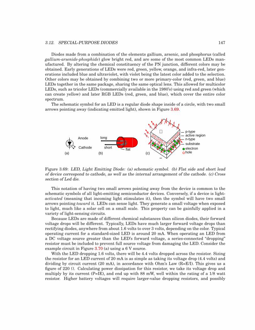
3.12. SPECIAL-PURPOSE DIODES 147
Diodes made from a combination of the elements gallium, arsenic, and phosphorus (calledgallium-arsenide-phosphide) glow bright red, and are some of the most common LEDs man-ufactured. By altering the chemical constituency of the PN junction, different colors may beobtained. Early generations of LEDs were red, green, yellow, orange, and infra-red, later gen-erations included blue and ultraviolet, with violet being the latest color added to the selection.Other colors may be obtained by combining two or more primary-color (red, green, and blue)LEDs together in the same package, sharing the same optical lens. This allowed for multicolorLEDs, such as tricolor LEDs (commercially available in the 1980’s) using red and green (whichcan create yellow) and later RGB LEDs (red, green, and blue), which cover the entire colorspectrum.
The schematic symbol for an LED is a regular diode shape inside of a circle, with two smallarrows pointing away (indicating emitted light), shown in Figure 3.69.
Anode
Cathode short
long
flat(a) (b)
substraten-typeactive regionp-type+
−
electronhole(c)
Figure 3.69: LED, Light Emitting Diode: (a) schematic symbol. (b) Flat side and short leadof device correspond to cathode, as well as the internal arrangement of the cathode. (c) Crosssection of Led die.
This notation of having two small arrows pointing away from the device is common to theschematic symbols of all light-emitting semiconductor devices. Conversely, if a device is light-activated (meaning that incoming light stimulates it), then the symbol will have two smallarrows pointing toward it. LEDs can sense light. They generate a small voltage when exposedto light, much like a solar cell on a small scale. This property can be gainfully applied in avariety of light-sensing circuits.
Because LEDs are made of different chemical substances than silicon diodes, their forwardvoltage drops will be different. Typically, LEDs have much larger forward voltage drops thanrectifying diodes, anywhere from about 1.6 volts to over 3 volts, depending on the color. Typicaloperating current for a standard-sized LED is around 20 mA. When operating an LED froma DC voltage source greater than the LED’s forward voltage, a series-connected “dropping”resistor must be included to prevent full source voltage from damaging the LED. Consider theexample circuit in Figure 3.70 (a) using a 6 V source.
With the LED dropping 1.6 volts, there will be 4.4 volts dropped across the resistor. Sizingthe resistor for an LED current of 20 mA is as simple as taking its voltage drop (4.4 volts) anddividing by circuit current (20 mA), in accordance with Ohm’s Law (R=E/I). This gives us afigure of 220 Ω. Calculating power dissipation for this resistor, we take its voltage drop andmultiply by its current (P=IE), and end up with 88 mW, well within the rating of a 1/8 wattresistor. Higher battery voltages will require larger-value dropping resistors, and possibly
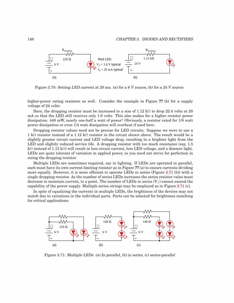
148 CHAPTER 3. DIODES AND RECTIFIERS
6 V
Red LED,
VF = 1.6 V typical
IF = 20 mA typical
Rdropping
220 Ω+
−
Rdropping
24 V
1.12 kΩ+
−(a) (b)
Figure 3.70: Setting LED current at 20 ma. (a) for a 6 V source, (b) for a 24 V source.
higher-power rating resistors as well. Consider the example in Figure ?? (b) for a supplyvoltage of 24 volts:
Here, the dropping resistor must be increased to a size of 1.12 kΩ to drop 22.4 volts at 20mA so that the LED still receives only 1.6 volts. This also makes for a higher resistor powerdissipation: 448 mW, nearly one-half a watt of power! Obviously, a resistor rated for 1/8 wattpower dissipation or even 1/4 watt dissipation will overheat if used here.
Dropping resistor values need not be precise for LED circuits. Suppose we were to use a1 kΩ resistor instead of a 1.12 kΩ resistor in the circuit shown above. The result would be aslightly greater circuit current and LED voltage drop, resulting in a brighter light from theLED and slightly reduced service life. A dropping resistor with too much resistance (say, 1.5kΩ instead of 1.12 kΩ) will result in less circuit current, less LED voltage, and a dimmer light.LEDs are quite tolerant of variation in applied power, so you need not strive for perfection insizing the dropping resistor.
Multiple LEDs are sometimes required, say in lighting. If LEDs are operated in parallel,each must have its own current limiting resistor as in Figure ?? (a) to ensure currents dividingmore equally. However, it is more efficient to operate LEDs in series (Figure 3.71 (b)) with asingle dropping resistor. As the number of series LEDs increases the series resistor value mustdecrease to maintain current, to a point. The number of LEDs in series (Vf ) cannot exceed thecapability of the power supply. Multiple series strings may be employed as in Figure 3.71 (c).
In spite of equalizing the currents in multiple LEDs, the brightness of the devices may notmatch due to variations in the individual parts. Parts can be selected for brightness matchingfor critical applications.
6 V
140 Ω+
−(a)
6 V
220 Ω +
−6 V
+
−
140 Ω
(b) (c)
Figure 3.71: Multiple LEDs: (a) In parallel, (b) in series, (c) series-parallel
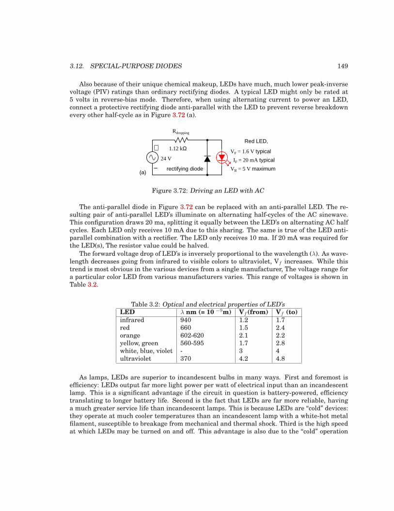
3.12. SPECIAL-PURPOSE DIODES 149
Also because of their unique chemical makeup, LEDs have much, much lower peak-inversevoltage (PIV) ratings than ordinary rectifying diodes. A typical LED might only be rated at5 volts in reverse-bias mode. Therefore, when using alternating current to power an LED,connect a protective rectifying diode anti-parallel with the LED to prevent reverse breakdownevery other half-cycle as in Figure 3.72 (a).
Red LED,
VF = 1.6 V typical
IF = 20 mA typical
Rdropping
1.12 kΩ
24 V
VR = 5 V maximumrectifying diode
+
−(a)
Figure 3.72: Driving an LED with AC
The anti-parallel diode in Figure 3.72 can be replaced with an anti-parallel LED. The re-sulting pair of anti-parallel LED’s illuminate on alternating half-cycles of the AC sinewave.This configuration draws 20 ma, splitting it equally between the LED’s on alternating AC halfcycles. Each LED only receives 10 mA due to this sharing. The same is true of the LED anti-parallel combination with a rectifier. The LED only receives 10 ma. If 20 mA was required forthe LED(s), The resistor value could be halved.
The forward voltage drop of LED’s is inversely proportional to the wavelength (λ). As wave-length decreases going from infrared to visible colors to ultraviolet, Vf increases. While thistrend is most obvious in the various devices from a single manufacturer, The voltage range fora particular color LED from various manufacturers varies. This range of voltages is shown inTable 3.2.
Table 3.2: Optical and electrical properties of LED’sLED λ nm (= 10 −9m) Vf (from) Vf (to)
infrared 940 1.2 1.7red 660 1.5 2.4orange 602-620 2.1 2.2yellow, green 560-595 1.7 2.8white, blue, violet - 3 4ultraviolet 370 4.2 4.8
As lamps, LEDs are superior to incandescent bulbs in many ways. First and foremost isefficiency: LEDs output far more light power per watt of electrical input than an incandescentlamp. This is a significant advantage if the circuit in question is battery-powered, efficiencytranslating to longer battery life. Second is the fact that LEDs are far more reliable, havinga much greater service life than incandescent lamps. This is because LEDs are “cold” devices:they operate at much cooler temperatures than an incandescent lamp with a white-hot metalfilament, susceptible to breakage from mechanical and thermal shock. Third is the high speedat which LEDs may be turned on and off. This advantage is also due to the “cold” operation
150 CHAPTER 3. DIODES AND RECTIFIERS
of LEDs: they don’t have to overcome thermal inertia in transitioning from off to on or viceversa. For this reason, LEDs are used to transmit digital (on/off) information as pulses of light,conducted in empty space or through fiber-optic cable, at very high rates of speed (millions ofpulses per second).
LEDs excel in monochromatic lighting applications like traffic signals and automotive taillights. Incandescents are abysmal in this application since they require filtering, decreasingefficiency. LEDs do not require filtering.
One major disadvantage of using LEDs as sources of illumination is their monochromatic(single-color) emission. No one wants to read a book under the light of a red, green, or blueLED. However, if used in combination, LED colors may be mixed for a more broad-spectrumglow. A new broad spectrum light source is the white LED. While small white panel indicatorshave been available for many years, illumination grade devices are still in development.
Table 3.3: Efficiency of lightingLamp type Efficiency lumen/watt Life hrs notes
White LED 35 100,000 costlyWhite LED, future 100 100,000 R&D targetIncandescent 12 1000 inexpensiveHalogen 15-17 2000 high quality lightCompact fluorescent 50-100 10,000 cost effectiveSodium vapor, lp 70-200 20,000 outdoorMercury vapor 13-48 18,000 outdoor
A white LED is a blue LED exciting a phosphor which emits yellow light. The blue plusyellow approximates white light. The nature of the phosphor determines the characteristics ofthe light. A red phosphor may be added to improve the quality of the yellow plus blue mixtureat the expense of efficiency. Table 3.3 compares white illumination LEDs to expected futuredevices and other conventional lamps. Efficiency is measured in lumens of light output perwatt of input power. If the 50 lumens/watt device can be improved to 100 lumens/watt, whiteLEDs will be comparable to compact fluorescent lamps in efficiency.
LEDs in general have been a major subject of R&D since the 1960’s. Because of this itis impractical to cover all geometries, chemistries, and characteristics that have been createdover the decades. The early devices were relatively dim and took moderate currents. The ef-ficiencies have been improved in later generations to the point it is hazardous to look closelyand directly into an illuminated LED. This can result in eye damage, and the LEDs only re-quired a minor increase in dropping voltage (Vf) and current. Modern high intensity deviceshave reached 180 lumens using 0.7 Amps (82 lumens/watt, Luxeon Rebel series cool white),and even higher intensity models can use even higher currents with a corresponding increasein brightness. Other developments, such as quantum dots, are the subject of current research,so expect to see new things for these devices in the future
3.12.4 Laser diodes
The laser diode is a further development upon the regular light-emitting diode, or LED. Theterm “laser” itself is actually an acronym, despite the fact its often written in lower-case letters.
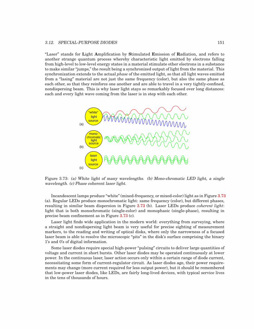
3.12. SPECIAL-PURPOSE DIODES 151
“Laser” stands for Light Amplification by Stimulated Emission of Radiation, and refers toanother strange quantum process whereby characteristic light emitted by electrons fallingfrom high-level to low-level energy states in a material stimulate other electrons in a substanceto make similar “jumps,” the result being a synchronized output of light from the material. Thissynchronization extends to the actual phase of the emitted light, so that all light waves emittedfrom a “lasing” material are not just the same frequency (color), but also the same phase aseach other, so that they reinforce one another and are able to travel in a very tightly-confined,nondispersing beam. This is why laser light stays so remarkably focused over long distances:each and every light wave coming from the laser is in step with each other.
(a)
(c)
(b)
"white"light
source
mono-chromatic
lightsource
laserlight
source
Figure 3.73: (a) White light of many wavelengths. (b) Mono-chromatic LED light, a singlewavelength. (c) Phase coherent laser light.
Incandescent lamps produce “white” (mixed-frequency, or mixed-color) light as in Figure 3.73(a). Regular LEDs produce monochromatic light: same frequency (color), but different phases,resulting in similar beam dispersion in Figure 3.73 (b). Laser LEDs produce coherent light:light that is both monochromatic (single-color) and monophasic (single-phase), resulting inprecise beam confinement as in Figure 3.73 (c).
Laser light finds wide application in the modern world: everything from surveying, wherea straight and nondispersing light beam is very useful for precise sighting of measurementmarkers, to the reading and writing of optical disks, where only the narrowness of a focusedlaser beam is able to resolve the microscopic “pits” in the disk’s surface comprising the binary1’s and 0’s of digital information.
Some laser diodes require special high-power “pulsing” circuits to deliver large quantities ofvoltage and current in short bursts. Other laser diodes may be operated continuously at lowerpower. In the continuous laser, laser action occurs only within a certain range of diode current,necessitating some form of current-regulator circuit. As laser diodes age, their power require-ments may change (more current required for less output power), but it should be rememberedthat low-power laser diodes, like LEDs, are fairly long-lived devices, with typical service livesin the tens of thousands of hours.
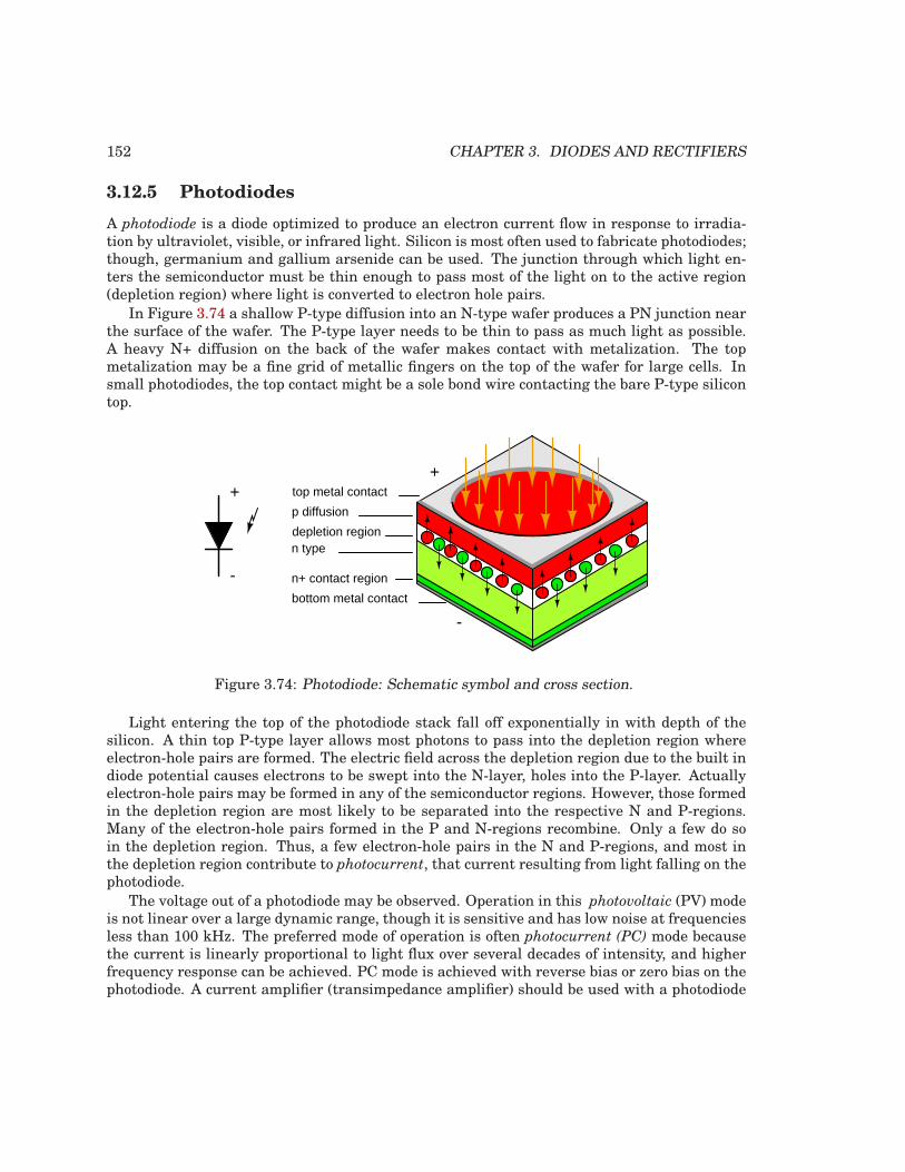
152 CHAPTER 3. DIODES AND RECTIFIERS
3.12.5 Photodiodes
A photodiode is a diode optimized to produce an electron current flow in response to irradia-tion by ultraviolet, visible, or infrared light. Silicon is most often used to fabricate photodiodes;though, germanium and gallium arsenide can be used. The junction through which light en-ters the semiconductor must be thin enough to pass most of the light on to the active region(depletion region) where light is converted to electron hole pairs.
In Figure 3.74 a shallow P-type diffusion into an N-type wafer produces a PN junction nearthe surface of the wafer. The P-type layer needs to be thin to pass as much light as possible.A heavy N+ diffusion on the back of the wafer makes contact with metalization. The topmetalization may be a fine grid of metallic fingers on the top of the wafer for large cells. Insmall photodiodes, the top contact might be a sole bond wire contacting the bare P-type silicontop.
depletion region
n+ contact region
n type
p diffusion
top metal contact
bottom metal contact
+
-
+
-
Figure 3.74: Photodiode: Schematic symbol and cross section.
Light entering the top of the photodiode stack fall off exponentially in with depth of thesilicon. A thin top P-type layer allows most photons to pass into the depletion region whereelectron-hole pairs are formed. The electric field across the depletion region due to the built indiode potential causes electrons to be swept into the N-layer, holes into the P-layer. Actuallyelectron-hole pairs may be formed in any of the semiconductor regions. However, those formedin the depletion region are most likely to be separated into the respective N and P-regions.Many of the electron-hole pairs formed in the P and N-regions recombine. Only a few do soin the depletion region. Thus, a few electron-hole pairs in the N and P-regions, and most inthe depletion region contribute to photocurrent, that current resulting from light falling on thephotodiode.
The voltage out of a photodiode may be observed. Operation in this photovoltaic (PV) modeis not linear over a large dynamic range, though it is sensitive and has low noise at frequenciesless than 100 kHz. The preferred mode of operation is often photocurrent (PC) mode becausethe current is linearly proportional to light flux over several decades of intensity, and higherfrequency response can be achieved. PC mode is achieved with reverse bias or zero bias on thephotodiode. A current amplifier (transimpedance amplifier) should be used with a photodiode
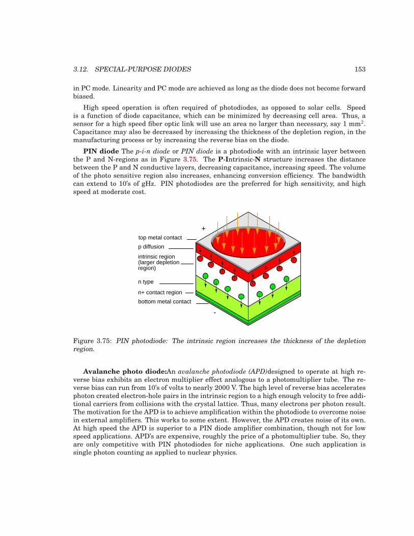
3.12. SPECIAL-PURPOSE DIODES 153
in PC mode. Linearity and PC mode are achieved as long as the diode does not become forwardbiased.
High speed operation is often required of photodiodes, as opposed to solar cells. Speedis a function of diode capacitance, which can be minimized by decreasing cell area. Thus, asensor for a high speed fiber optic link will use an area no larger than necessary, say 1 mm2.Capacitance may also be decreased by increasing the thickness of the depletion region, in themanufacturing process or by increasing the reverse bias on the diode.
PIN diode The p-i-n diode or PIN diode is a photodiode with an intrinsic layer betweenthe P and N-regions as in Figure 3.75. The P-Intrinsic-N structure increases the distancebetween the P and N conductive layers, decreasing capacitance, increasing speed. The volumeof the photo sensitive region also increases, enhancing conversion efficiency. The bandwidthcan extend to 10’s of gHz. PIN photodiodes are the preferred for high sensitivity, and highspeed at moderate cost.
intrinsic region(larger depletionregion)
n+ contact region
n type
p diffusion
top metal contact
bottom metal contact
+
-
Figure 3.75: PIN photodiode: The intrinsic region increases the thickness of the depletionregion.
Avalanche photo diode:An avalanche photodiode (APD)designed to operate at high re-verse bias exhibits an electron multiplier effect analogous to a photomultiplier tube. The re-verse bias can run from 10’s of volts to nearly 2000 V. The high level of reverse bias acceleratesphoton created electron-hole pairs in the intrinsic region to a high enough velocity to free addi-tional carriers from collisions with the crystal lattice. Thus, many electrons per photon result.The motivation for the APD is to achieve amplification within the photodiode to overcome noisein external amplifiers. This works to some extent. However, the APD creates noise of its own.At high speed the APD is superior to a PIN diode amplifier combination, though not for lowspeed applications. APD’s are expensive, roughly the price of a photomultiplier tube. So, theyare only competitive with PIN photodiodes for niche applications. One such application issingle photon counting as applied to nuclear physics.
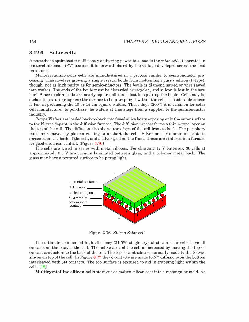
154 CHAPTER 3. DIODES AND RECTIFIERS
3.12.6 Solar cells
A photodiode optimized for efficiently delivering power to a load is the solar cell. It operates inphotovoltaic mode (PV) because it is forward biased by the voltage developed across the loadresistance.
Monocrystalline solar cells are manufactured in a process similar to semiconductor pro-cessing. This involves growing a single crystal boule from molten high purity silicon (P-type),though, not as high purity as for semiconductors. The boule is diamond sawed or wire sawedinto wafers. The ends of the boule must be discarded or recycled, and silicon is lost in the sawkerf. Since modern cells are nearly square, silicon is lost in squaring the boule. Cells may beetched to texture (roughen) the surface to help trap light within the cell. Considerable siliconis lost in producing the 10 or 15 cm square wafers. These days (2007) it is common for solarcell manufacturer to purchase the wafers at this stage from a supplier to the semiconductorindustry.
P-typeWafers are loaded back-to-back into fused silica boats exposing only the outer surfaceto the N-type dopant in the diffusion furnace. The diffusion process forms a thin n-type layer onthe top of the cell. The diffusion also shorts the edges of the cell front to back. The peripherymust be removed by plasma etching to unshort the cell. Silver and or aluminum paste isscreened on the back of the cell, and a silver grid on the front. These are sintered in a furnacefor good electrical contact. (Figure 3.76)
The cells are wired in series with metal ribbons. For charging 12 V batteries, 36 cells atapproximately 0.5 V are vacuum laminated between glass, and a polymer metal back. Theglass may have a textured surface to help trap light.
depletion regionP type wafer
N diffusion
top metal contact
bottom metal contact
+
-
Figure 3.76: Silicon Solar cell
The ultimate commercial high efficiency (21.5%) single crystal silicon solar cells have allcontacts on the back of the cell. The active area of the cell is increased by moving the top (-)contact conductors to the back of the cell. The top (-) contacts are normally made to the N-typesilicon on top of the cell. In Figure 3.77 the (-) contacts are made to N+ diffusions on the bottominterleaved with (+) contacts. The top surface is textured to aid in trapping light within thecell.. [18]
Multicyrstalline silicon cells start out as molten silicon cast into a rectangular mold. As
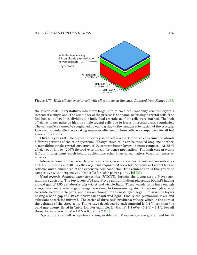
3.12. SPECIAL-PURPOSE DIODES 155
Silicon dioxide passivationAntireflectrive coating
N-type diffusion
P-type wafer
N+ diffusion
P+ diffusion
- contact
+ contact
N+ diffusion- contact
Figure 3.77: High efficiency solar cell with all contacts on the back. Adapted from Figure 1 [18]
the silicon cools, it crystallizes into a few large (mm to cm sized) randomly oriented crystalsinstead of a single one. The remainder of the process is the same as for single crystal cells. Thefinished cells show lines dividing the individual crystals, as if the cells were cracked. The highefficiency is not quite as high as single crystal cells due to losses at crystal grain boundaries.The cell surface cannot be roughened by etching due to the random orientation of the crystals.However, an antireflectrive coating improves efficiency. These cells are competitive for all butspace applications.
Three layer cell: The highest efficiency solar cell is a stack of three cells tuned to absorbdifferent portions of the solar spectrum. Though three cells can be stacked atop one another,a monolithic single crystal structure of 20 semiconductor layers is more compact. At 32 %efficiency, it is now (2007) favored over silicon for space application. The high cost preventsit from finding many earth bound applications other than concentrators based on lenses ormirrors.
Intensive research has recently produced a version enhanced for terrestrial concentratorsat 400 - 1000 suns and 40.7% efficiency. This requires either a big inexpensive Fresnel lens orreflector and a small area of the expensive semiconductor. This combination is thought to becompetitive with inexpensive silicon cells for solar power plants. [9] [23]
Metal organic chemical vapor deposition (MOCVD) deposits the layers atop a P-type ger-manium substrate. The top layers of N and P-type gallium indium phosphide (GaInP) havinga band gap of 1.85 eV, absorbs ultraviolet and visible light. These wavelengths have enoughenergy to exceed the band gap. Longer wavelengths (lower energy) do not have enough energyto create electron-hole pairs, and pass on through to the next layer. A gallium arsenide layershaving a band gap of 1.42 eV, absorbs near infrared light. Finally the germanium layer andsubstrate absorb far infrared. The series of three cells produce a voltage which is the sum ofthe voltages of the three cells. The voltage developed by each material is 0.4 V less than theband gap energy listed in Table 3.4. For example, for GaInP: 1.8 eV/e - 0.4 V = 1.4 V. For allthree the voltage is 1.4 V + 1.0 V + 0.3 V = 2.7 V. [4]
Crystalline solar cell arrays have a long usable life. Many arrays are guaranteed for 25
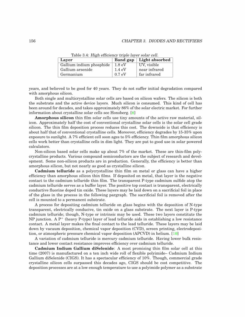
156 CHAPTER 3. DIODES AND RECTIFIERS
Table 3.4: High efficiency triple layer solar cell.Layer Band gap Light absorbed
Gallium indium phosphide 1.8 eV UV, visibleGallium arsenide 1.4 eV near infraredGermanium 0.7 eV far infrared
years, and believed to be good for 40 years. They do not suffer initial degradation comparedwith amorphous silicon.
Both single and multicrystalline solar cells are based on silicon wafers. The silicon is boththe substrate and the active device layers. Much silicon is consumed. This kind of cell hasbeen around for decades, and takes approximately 86% of the solar electric market. For furtherinformation about crystalline solar cells see Honsberg. [8]
Amorphous silicon thin film solar cells use tiny amounts of the active raw material, sil-icon. Approximately half the cost of conventional crystalline solar cells is the solar cell gradesilicon. The thin film deposition process reduces this cost. The downside is that efficiency isabout half that of conventional crystalline cells. Moreover, efficiency degrades by 15-35% uponexposure to sunlight. A 7% efficient cell soon ages to 5% efficiency. Thin film amorphous siliconcells work better than crystalline cells in dim light. They are put to good use in solar poweredcalculators.
Non-silicon based solar cells make up about 7% of the market. These are thin-film poly-crystalline products. Various compound semiconductors are the subject of research and devel-opment. Some non-silicon products are in production. Generally, the efficiency is better thanamorphous silicon, but not nearly as good as crystalline silicon.
Cadmium telluride as a polycrystalline thin film on metal or glass can have a higherefficiency than amorphous silicon thin films. If deposited on metal, that layer is the negativecontact to the cadmium telluride thin film. The transparent P-type cadmium sulfide atop thecadmium telluride serves as a buffer layer. The positive top contact is transparent, electricallyconductive fluorine doped tin oxide. These layers may be laid down on a sacrificial foil in placeof the glass in the process in the following pargraph. The sacrificial foil is removed after thecell is mounted to a permanent substrate.
A process for depositing cadmium telluride on glass begins with the deposition of N-typetransparent, electrically conducive, tin oxide on a glass substrate. The next layer is P-typecadmium telluride; though, N-type or intrinsic may be used. These two layers constitute theNP junction. A P+ (heavy P-type) layer of lead telluride aids in establishing a low resistancecontact. A metal layer makes the final contact to the lead telluride. These layers may be laiddown by vacuum deposition, chemical vapor deposition (CVD), screen printing, electrodeposi-tion, or atmospheric pressure chemical vapor deposition (APCVD) in helium. [10]
A variation of cadmium telluride is mercury cadmium telluride. Having lower bulk resis-tance and lower contact resistance improves efficiency over cadmium telluride.
Cadmium Indium Gallium diSelenide: A most promising thin film solar cell at thistime (2007) is manufactured on a ten inch wide roll of flexible polyimide– Cadmium IndiumGallium diSelenide (CIGS). It has a spectacular efficiency of 10%. Though, commercial gradecrystalline silicon cells surpassed this decades ago, CIGS should be cost competitive. Thedeposition processes are at a low enough temperature to use a polyimide polymer as a substrate
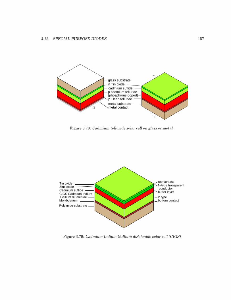
3.12. SPECIAL-PURPOSE DIODES 157
-
n Tin oxide cadmium suflide
metal contact
p+ lead telluride
p cadmium telluride(phosphorus doped)
metal substrate
glass substrate−
+
+
Figure 3.78: Cadmium telluride solar cell on glass or metal.
-
Polyimide substrate
Molybdenum
CIGS Cadmium Indium Gallium diSelenide
Zinc oxideTin oxide
Cadmium suflide
N-type transparent conductor
P type
buffer layer
bottom contact
top contact
Figure 3.79: Cadmium Indium Gallium diSelenide solar cell (CIGS)

158 CHAPTER 3. DIODES AND RECTIFIERS
instead of metal or glass. (Figure 3.79) The CIGS is manufactured in a roll to roll process,which should drive down costs. GIGS cells may also be produced by an inherently low costelectrochemical process. [7]
• REVIEW:
• Most solar cells are silicon single crystal or multicrystal because of their good efficiencyand moderate cost.
• Less efficient thin films of various amorphous or polycrystalline materials comprise therest of the market.
• Table 3.5 compares selected solar cells.
Table 3.5: Solar cell propertiesSolar cell type Maximum
effi-
ciency
Practical
effi-
ciency
Notes
Selenium, polycrystalline 0.7% - 1883, Charles FrittsSilicon, single crystal - 4% 1950’s, first silicon solar cellSilicon, single crystal PERL,terrestrial, space
25% - solar cars, cost=100x commer-cial
Silicon, single crystal, commer-cial terrestrial
24% 14-17% $5-$10/peak watt
Cypress Semiconductor, Sun-power, silicon single crystal
21.5% 19% all contacts on cell back
Gallium Indium Phosphide/Gallium Arsenide/ Germa-nium, single crystal, multilayer
- 32% Preferred for space.
Advanced terrestrial version ofabove.
- 40.7% Uses optical concentrator.
Silicon, multicrystalline 18.5% 15.5% -Thin films, - - -Silicon, amorphous 13% 5-7% Degrades in sun light. Good in-
doors for calculators or cloudyoutdoors.
Cadmium telluride, polycrys-talline
16% - glass or metal substrate
Copper indium arsenide dise-lenide, polycrystalline
18% 10% 10 inch flexible polymer web.[17]
Organic polymer, 100% plastic 4.5% - R&D project
3.12.7 Varicap or varactor diodes
A variable capacitance diode is known as a varicap diode or as a varactor. If a diode is reversebiased, an insulating depletion region forms between the two semiconductive layers. In many
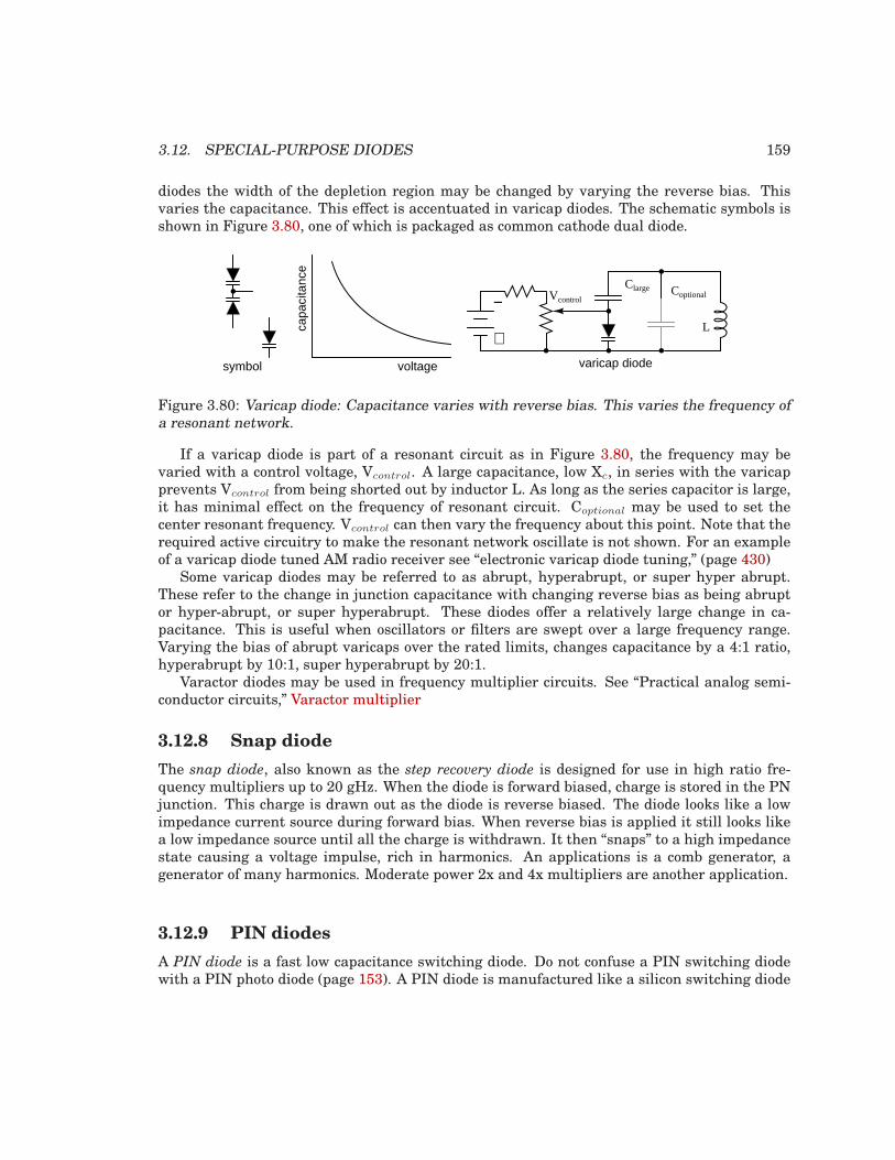
3.12. SPECIAL-PURPOSE DIODES 159
diodes the width of the depletion region may be changed by varying the reverse bias. Thisvaries the capacitance. This effect is accentuated in varicap diodes. The schematic symbols isshown in Figure 3.80, one of which is packaged as common cathode dual diode.
−
+
Clarge Coptional
varicap diode
Vcontrol
L
symbol voltage
capa
cita
nce
Figure 3.80: Varicap diode: Capacitance varies with reverse bias. This varies the frequency ofa resonant network.
If a varicap diode is part of a resonant circuit as in Figure 3.80, the frequency may bevaried with a control voltage, Vcontrol. A large capacitance, low Xc, in series with the varicapprevents Vcontrol from being shorted out by inductor L. As long as the series capacitor is large,it has minimal effect on the frequency of resonant circuit. Coptional may be used to set thecenter resonant frequency. Vcontrol can then vary the frequency about this point. Note that therequired active circuitry to make the resonant network oscillate is not shown. For an exampleof a varicap diode tuned AM radio receiver see “electronic varicap diode tuning,” (page 430)
Some varicap diodes may be referred to as abrupt, hyperabrupt, or super hyper abrupt.These refer to the change in junction capacitance with changing reverse bias as being abruptor hyper-abrupt, or super hyperabrupt. These diodes offer a relatively large change in ca-pacitance. This is useful when oscillators or filters are swept over a large frequency range.Varying the bias of abrupt varicaps over the rated limits, changes capacitance by a 4:1 ratio,hyperabrupt by 10:1, super hyperabrupt by 20:1.
Varactor diodes may be used in frequency multiplier circuits. See “Practical analog semi-conductor circuits,” Varactor multiplier
3.12.8 Snap diode
The snap diode, also known as the step recovery diode is designed for use in high ratio fre-quency multipliers up to 20 gHz. When the diode is forward biased, charge is stored in the PNjunction. This charge is drawn out as the diode is reverse biased. The diode looks like a lowimpedance current source during forward bias. When reverse bias is applied it still looks likea low impedance source until all the charge is withdrawn. It then “snaps” to a high impedancestate causing a voltage impulse, rich in harmonics. An applications is a comb generator, agenerator of many harmonics. Moderate power 2x and 4x multipliers are another application.
3.12.9 PIN diodes
A PIN diode is a fast low capacitance switching diode. Do not confuse a PIN switching diodewith a PIN photo diode (page 153). A PIN diode is manufactured like a silicon switching diode
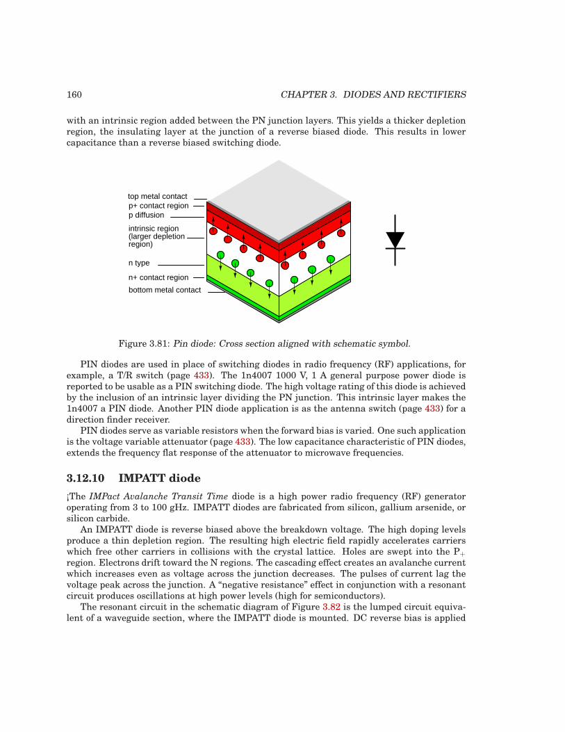
160 CHAPTER 3. DIODES AND RECTIFIERS
with an intrinsic region added between the PN junction layers. This yields a thicker depletionregion, the insulating layer at the junction of a reverse biased diode. This results in lowercapacitance than a reverse biased switching diode.
intrinsic region(larger depletionregion)
n+ contact region
n type
p diffusion
top metal contact
bottom metal contact
p+ contact region
Figure 3.81: Pin diode: Cross section aligned with schematic symbol.
PIN diodes are used in place of switching diodes in radio frequency (RF) applications, forexample, a T/R switch (page 433). The 1n4007 1000 V, 1 A general purpose power diode isreported to be usable as a PIN switching diode. The high voltage rating of this diode is achievedby the inclusion of an intrinsic layer dividing the PN junction. This intrinsic layer makes the1n4007 a PIN diode. Another PIN diode application is as the antenna switch (page 433) for adirection finder receiver.
PIN diodes serve as variable resistors when the forward bias is varied. One such applicationis the voltage variable attenuator (page 433). The low capacitance characteristic of PIN diodes,extends the frequency flat response of the attenuator to microwave frequencies.
3.12.10 IMPATT diode
¡The IMPact Avalanche Transit Time diode is a high power radio frequency (RF) generatoroperating from 3 to 100 gHz. IMPATT diodes are fabricated from silicon, gallium arsenide, orsilicon carbide.
An IMPATT diode is reverse biased above the breakdown voltage. The high doping levelsproduce a thin depletion region. The resulting high electric field rapidly accelerates carrierswhich free other carriers in collisions with the crystal lattice. Holes are swept into the P+
region. Electrons drift toward the N regions. The cascading effect creates an avalanche currentwhich increases even as voltage across the junction decreases. The pulses of current lag thevoltage peak across the junction. A “negative resistance” effect in conjunction with a resonantcircuit produces oscillations at high power levels (high for semiconductors).
The resonant circuit in the schematic diagram of Figure 3.82 is the lumped circuit equiva-lent of a waveguide section, where the IMPATT diode is mounted. DC reverse bias is applied
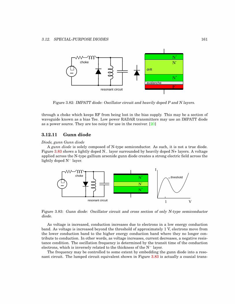
3.12. SPECIAL-PURPOSE DIODES 161
+−
N+
P+
drift
avalanche
choke
resonant circuit
N-N+
Figure 3.82: IMPATT diode: Oscillator circuit and heavily doped P and N layers.
through a choke which keeps RF from being lost in the bias supply. This may be a section ofwaveguide known as a bias Tee. Low power RADAR transmitters may use an IMPATT diodeas a power source. They are too noisy for use in the receiver. [20]
3.12.11 Gunn diode
Diode, gunn Gunn diode
A gunn diode is solely composed of N-type semiconductor. As such, it is not a true diode.Figure 3.83 shows a lightly doped N
−layer surrounded by heavily doped N+ layers. A voltage
applied across the N-type gallium arsenide gunn diode creates a strong electric field across thelightly doped N− layer.
+−
N+
choke
resonant circuit
N-
N+
V1
I
threshold
Figure 3.83: Gunn diode: Oscillator circuit and cross section of only N-type semiconductordiode.
As voltage is increased, conduction increases due to electrons in a low energy conductionband. As voltage is increased beyond the threshold of approximately 1 V, electrons move fromthe lower conduction band to the higher energy conduction band where they no longer con-tribute to conduction. In other words, as voltage increases, current decreases, a negative resis-tance condition. The oscillation frequency is determined by the transit time of the conductionelectrons, which is inversely related to the thickness of the N− layer.
The frequency may be controlled to some extent by embedding the gunn diode into a reso-nant circuit. The lumped circuit equivalent shown in Figure 3.83 is actually a coaxial trans-
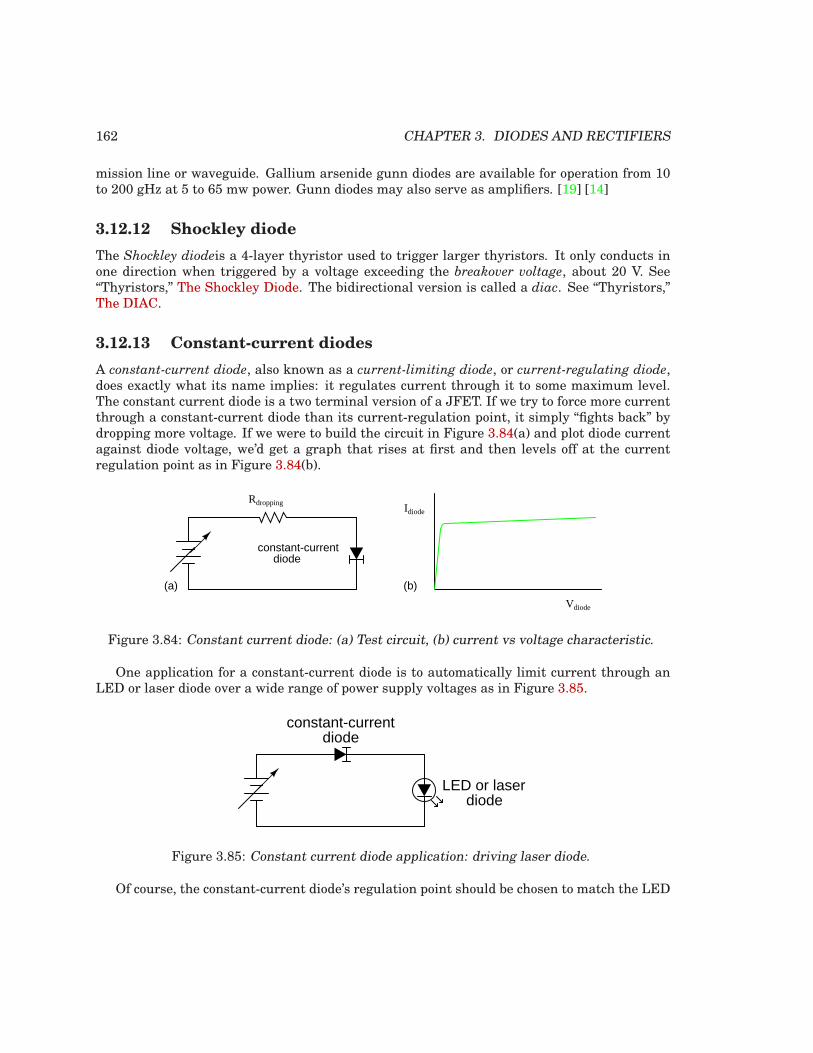
162 CHAPTER 3. DIODES AND RECTIFIERS
mission line or waveguide. Gallium arsenide gunn diodes are available for operation from 10to 200 gHz at 5 to 65 mw power. Gunn diodes may also serve as amplifiers. [19] [14]
3.12.12 Shockley diode
The Shockley diodeis a 4-layer thyristor used to trigger larger thyristors. It only conducts inone direction when triggered by a voltage exceeding the breakover voltage, about 20 V. See“Thyristors,” The Shockley Diode. The bidirectional version is called a diac. See “Thyristors,”The DIAC.
3.12.13 Constant-current diodes
A constant-current diode, also known as a current-limiting diode, or current-regulating diode,does exactly what its name implies: it regulates current through it to some maximum level.The constant current diode is a two terminal version of a JFET. If we try to force more currentthrough a constant-current diode than its current-regulation point, it simply “fights back” bydropping more voltage. If we were to build the circuit in Figure 3.84(a) and plot diode currentagainst diode voltage, we’d get a graph that rises at first and then levels off at the currentregulation point as in Figure 3.84(b).
Rdropping
constant-current diode
Vdiode
Idiode
(a) (b)
Figure 3.84: Constant current diode: (a) Test circuit, (b) current vs voltage characteristic.
One application for a constant-current diode is to automatically limit current through anLED or laser diode over a wide range of power supply voltages as in Figure 3.85.
constant-currentdiode
LED or laserdiode
Figure 3.85: Constant current diode application: driving laser diode.
Of course, the constant-current diode’s regulation point should be chosen to match the LED
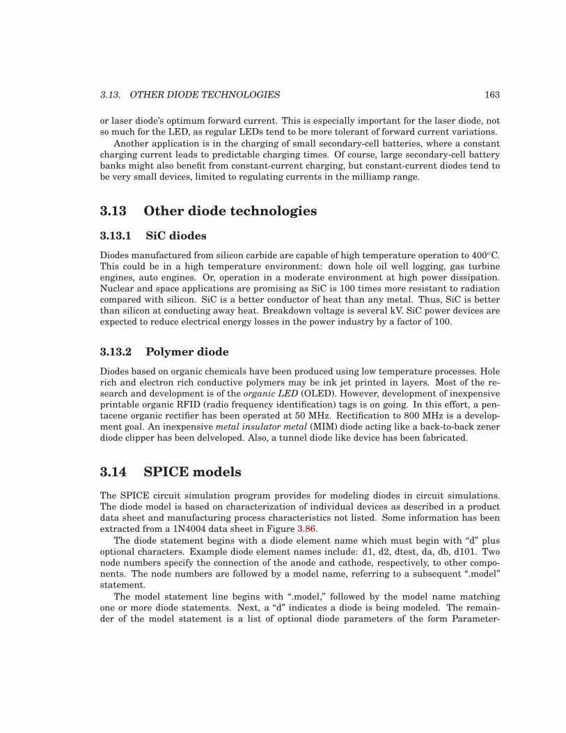
3.13. OTHER DIODE TECHNOLOGIES 163
or laser diode’s optimum forward current. This is especially important for the laser diode, notso much for the LED, as regular LEDs tend to be more tolerant of forward current variations.
Another application is in the charging of small secondary-cell batteries, where a constantcharging current leads to predictable charging times. Of course, large secondary-cell batterybanks might also benefit from constant-current charging, but constant-current diodes tend tobe very small devices, limited to regulating currents in the milliamp range.
3.13 Other diode technologies
3.13.1 SiC diodes
Diodes manufactured from silicon carbide are capable of high temperature operation to 400oC.This could be in a high temperature environment: down hole oil well logging, gas turbineengines, auto engines. Or, operation in a moderate environment at high power dissipation.Nuclear and space applications are promising as SiC is 100 times more resistant to radiationcompared with silicon. SiC is a better conductor of heat than any metal. Thus, SiC is betterthan silicon at conducting away heat. Breakdown voltage is several kV. SiC power devices areexpected to reduce electrical energy losses in the power industry by a factor of 100.
3.13.2 Polymer diode
Diodes based on organic chemicals have been produced using low temperature processes. Holerich and electron rich conductive polymers may be ink jet printed in layers. Most of the re-search and development is of the organic LED (OLED). However, development of inexpensiveprintable organic RFID (radio frequency identification) tags is on going. In this effort, a pen-tacene organic rectifier has been operated at 50 MHz. Rectification to 800 MHz is a develop-ment goal. An inexpensive metal insulator metal (MIM) diode acting like a back-to-back zenerdiode clipper has been delveloped. Also, a tunnel diode like device has been fabricated.
3.14 SPICE models
The SPICE circuit simulation program provides for modeling diodes in circuit simulations.The diode model is based on characterization of individual devices as described in a productdata sheet and manufacturing process characteristics not listed. Some information has beenextracted from a 1N4004 data sheet in Figure 3.86.
The diode statement begins with a diode element name which must begin with “d” plusoptional characters. Example diode element names include: d1, d2, dtest, da, db, d101. Twonode numbers specify the connection of the anode and cathode, respectively, to other compo-nents. The node numbers are followed by a model name, referring to a subsequent “.model”statement.
The model statement line begins with “.model,” followed by the model name matchingone or more diode statements. Next, a “d” indicates a diode is being modeled. The remain-der of the model statement is a list of optional diode parameters of the form Parameter-
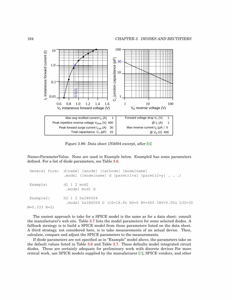
164 CHAPTER 3. DIODES AND RECTIFIERS
1
10
100
1 10 100
1.0
10
0.6 1.6
0.01
0.1
0.8 1.0 1.2 1.4VF instaneous forward voltage (V)
I F in
stan
eous
forw
ard
curr
ent (
I)
VR reverse voltage (V)
CJ
junc
tion
capa
cita
nce
(pF
)
30
0.92
5
Max avg rectified current IO (A) 1
Peak repetitive reverse voltage VRRM (V) 400
Peak forward surge current IFSM (A) 30
Forward voltage drop VF (V) 1
@ IF (A) 1
Max reverse current IR (µΑ) 5@ VR (V) 400Total capacitance CT (pF) 15
Figure 3.86: Data sheet 1N4004 excerpt, after [6].
Name=ParameterValue. None are used in Example below. Example2 has some parametersdefined. For a list of diode parameters, see Table 3.6.
General form: d[name] [anode] [cathode] [modelname].model ([modelname] d [parmtr1=x] [parmtr2=y] . . .)
Example: d1 1 2 mod1.model mod1 d
Example2: D2 1 2 Da1N4004.model Da1N4004 D (IS=18.8n RS=0 BV=400 IBV=5.00u CJO=30
M=0.333 N=2)
The easiest approach to take for a SPICE model is the same as for a data sheet: consultthe manufacturer’s web site. Table 3.7 lists the model parameters for some selected diodes. Afallback strategy is to build a SPICE model from those parameters listed on the data sheet.A third strategy, not considered here, is to take measurements of an actual device. Then,calculate, compare and adjust the SPICE parameters to the measurements.
If diode parameters are not specified as in “Example” model above, the parameters take onthe default values listed in Table 3.6 and Table 3.7. These defaults model integrated circuitdiodes. These are certainly adequate for preliminary work with discrete devices For morecritical work, use SPICE models supplied by the manufacturer [5], SPICE vendors, and other
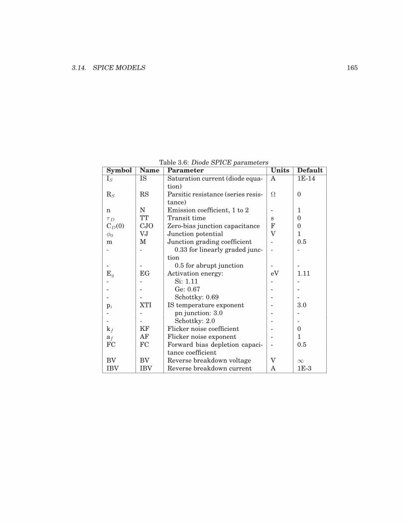
3.14. SPICE MODELS 165
Table 3.6: Diode SPICE parametersSymbol Name Parameter Units Default
IS IS Saturation current (diode equa-tion)
A 1E-14
RS RS Parsitic resistance (series resis-tance)
Ω 0
n N Emission coefficient, 1 to 2 - 1τD TT Transit time s 0CD(0) CJO Zero-bias junction capacitance F 0φ0 VJ Junction potential V 1m M Junction grading coefficient - 0.5- - 0.33 for linearly graded junc-
tion- -
- - 0.5 for abrupt junction - -Eg EG Activation energy: eV 1.11- - Si: 1.11 - -- - Ge: 0.67 - -- - Schottky: 0.69 - -pi XTI IS temperature exponent - 3.0- - pn junction: 3.0 - -- - Schottky: 2.0 - -kf KF Flicker noise coefficient - 0af AF Flicker noise exponent - 1FC FC Forward bias depletion capaci-
tance coefficient- 0.5
BV BV Reverse breakdown voltage V ∞IBV IBV Reverse breakdown current A 1E-3
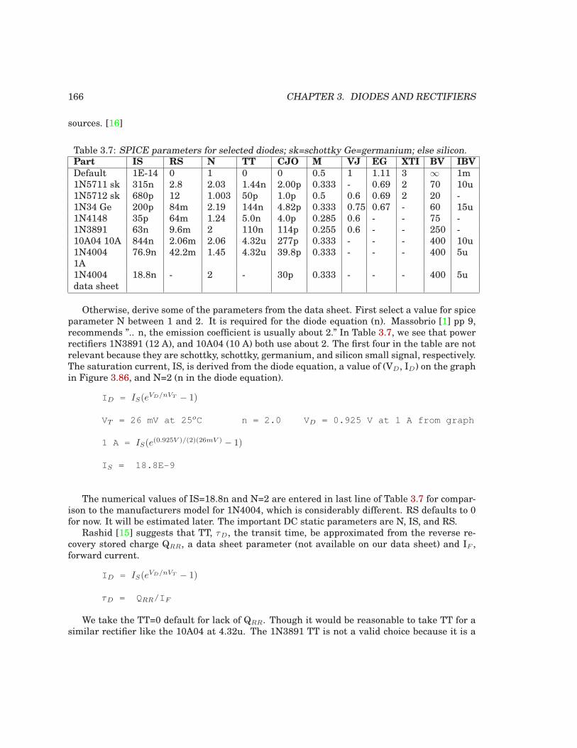
166 CHAPTER 3. DIODES AND RECTIFIERS
sources. [16]
Table 3.7: SPICE parameters for selected diodes; sk=schottky Ge=germanium; else silicon.Part IS RS N TT CJO M VJ EG XTI BV IBV
Default 1E-14 0 1 0 0 0.5 1 1.11 3 ∞ 1m1N5711 sk 315n 2.8 2.03 1.44n 2.00p 0.333 - 0.69 2 70 10u1N5712 sk 680p 12 1.003 50p 1.0p 0.5 0.6 0.69 2 20 -1N34 Ge 200p 84m 2.19 144n 4.82p 0.333 0.75 0.67 - 60 15u1N4148 35p 64m 1.24 5.0n 4.0p 0.285 0.6 - - 75 -1N3891 63n 9.6m 2 110n 114p 0.255 0.6 - - 250 -10A04 10A 844n 2.06m 2.06 4.32u 277p 0.333 - - - 400 10u1N40041A
76.9n 42.2m 1.45 4.32u 39.8p 0.333 - - - 400 5u
1N4004data sheet
18.8n - 2 - 30p 0.333 - - - 400 5u
Otherwise, derive some of the parameters from the data sheet. First select a value for spiceparameter N between 1 and 2. It is required for the diode equation (n). Massobrio [1] pp 9,recommends ”.. n, the emission coefficient is usually about 2.” In Table 3.7, we see that powerrectifiers 1N3891 (12 A), and 10A04 (10 A) both use about 2. The first four in the table are notrelevant because they are schottky, schottky, germanium, and silicon small signal, respectively.The saturation current, IS, is derived from the diode equation, a value of (VD, ID) on the graphin Figure 3.86, and N=2 (n in the diode equation).
I D = IS(eVD/nVT − 1)
VT = 26 mV at 25 oC n = 2.0 V D = 0.925 V at 1 A from graph
1 A = IS(e(0.925V )/(2)(26mV ) − 1)
I S = 18.8E-9
The numerical values of IS=18.8n and N=2 are entered in last line of Table 3.7 for compar-ison to the manufacturers model for 1N4004, which is considerably different. RS defaults to 0for now. It will be estimated later. The important DC static parameters are N, IS, and RS.
Rashid [15] suggests that TT, τD, the transit time, be approximated from the reverse re-covery stored charge QRR, a data sheet parameter (not available on our data sheet) and IF ,forward current.
I D = IS(eVD/nVT − 1)
τD = QRR/I F
We take the TT=0 default for lack of QRR. Though it would be reasonable to take TT for asimilar rectifier like the 10A04 at 4.32u. The 1N3891 TT is not a valid choice because it is a
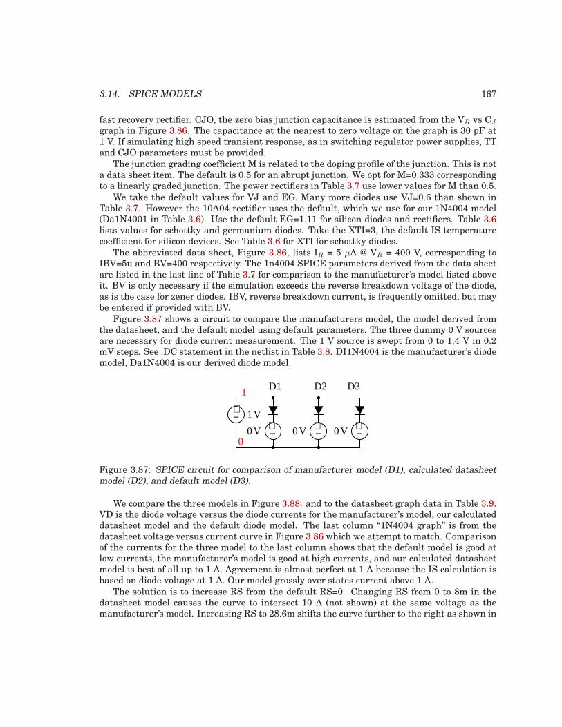
3.14. SPICE MODELS 167
fast recovery rectifier. CJO, the zero bias junction capacitance is estimated from the VR vs CJ
graph in Figure 3.86. The capacitance at the nearest to zero voltage on the graph is 30 pF at1 V. If simulating high speed transient response, as in switching regulator power supplies, TTand CJO parameters must be provided.
The junction grading coefficient M is related to the doping profile of the junction. This is nota data sheet item. The default is 0.5 for an abrupt junction. We opt for M=0.333 correspondingto a linearly graded junction. The power rectifiers in Table 3.7 use lower values for M than 0.5.
We take the default values for VJ and EG. Many more diodes use VJ=0.6 than shown inTable 3.7. However the 10A04 rectifier uses the default, which we use for our 1N4004 model(Da1N4001 in Table 3.6). Use the default EG=1.11 for silicon diodes and rectifiers. Table 3.6lists values for schottky and germanium diodes. Take the XTI=3, the default IS temperaturecoefficient for silicon devices. See Table 3.6 for XTI for schottky diodes.
The abbreviated data sheet, Figure 3.86, lists IR = 5 µA @ VR = 400 V, corresponding toIBV=5u and BV=400 respectively. The 1n4004 SPICE parameters derived from the data sheetare listed in the last line of Table 3.7 for comparison to the manufacturer’s model listed aboveit. BV is only necessary if the simulation exceeds the reverse breakdown voltage of the diode,as is the case for zener diodes. IBV, reverse breakdown current, is frequently omitted, but maybe entered if provided with BV.
Figure 3.87 shows a circuit to compare the manufacturers model, the model derived fromthe datasheet, and the default model using default parameters. The three dummy 0 V sourcesare necessary for diode current measurement. The 1 V source is swept from 0 to 1.4 V in 0.2mV steps. See .DC statement in the netlist in Table 3.8. DI1N4004 is the manufacturer’s diodemodel, Da1N4004 is our derived diode model.
0
+− 1V
D1 D21
+−0V+
−0V +−0V
D3
Figure 3.87: SPICE circuit for comparison of manufacturer model (D1), calculated datasheetmodel (D2), and default model (D3).
We compare the three models in Figure 3.88. and to the datasheet graph data in Table 3.9.VD is the diode voltage versus the diode currents for the manufacturer’s model, our calculateddatasheet model and the default diode model. The last column “1N4004 graph” is from thedatasheet voltage versus current curve in Figure 3.86 which we attempt to match. Comparisonof the currents for the three model to the last column shows that the default model is good atlow currents, the manufacturer’s model is good at high currents, and our calculated datasheetmodel is best of all up to 1 A. Agreement is almost perfect at 1 A because the IS calculation isbased on diode voltage at 1 A. Our model grossly over states current above 1 A.
The solution is to increase RS from the default RS=0. Changing RS from 0 to 8m in thedatasheet model causes the curve to intersect 10 A (not shown) at the same voltage as themanufacturer’s model. Increasing RS to 28.6m shifts the curve further to the right as shown in
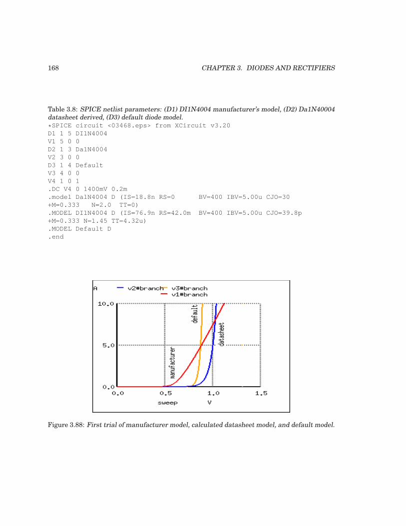
168 CHAPTER 3. DIODES AND RECTIFIERS
Table 3.8: SPICE netlist parameters: (D1) DI1N4004 manufacturer’s model, (D2) Da1N40004datasheet derived, (D3) default diode model.
* SPICE circuit <03468.eps> from XCircuit v3.20D1 1 5 DI1N4004V1 5 0 0D2 1 3 Da1N4004V2 3 0 0D3 1 4 DefaultV3 4 0 0V4 1 0 1.DC V4 0 1400mV 0.2m.model Da1N4004 D (IS=18.8n RS=0 BV=400 IBV=5.00u CJO=30+M=0.333 N=2.0 TT=0).MODEL DI1N4004 D (IS=76.9n RS=42.0m BV=400 IBV=5.00u CJO= 39.8p+M=0.333 N=1.45 TT=4.32u).MODEL Default D.end
Figure 3.88: First trial of manufacturer model, calculated datasheet model, and default model.
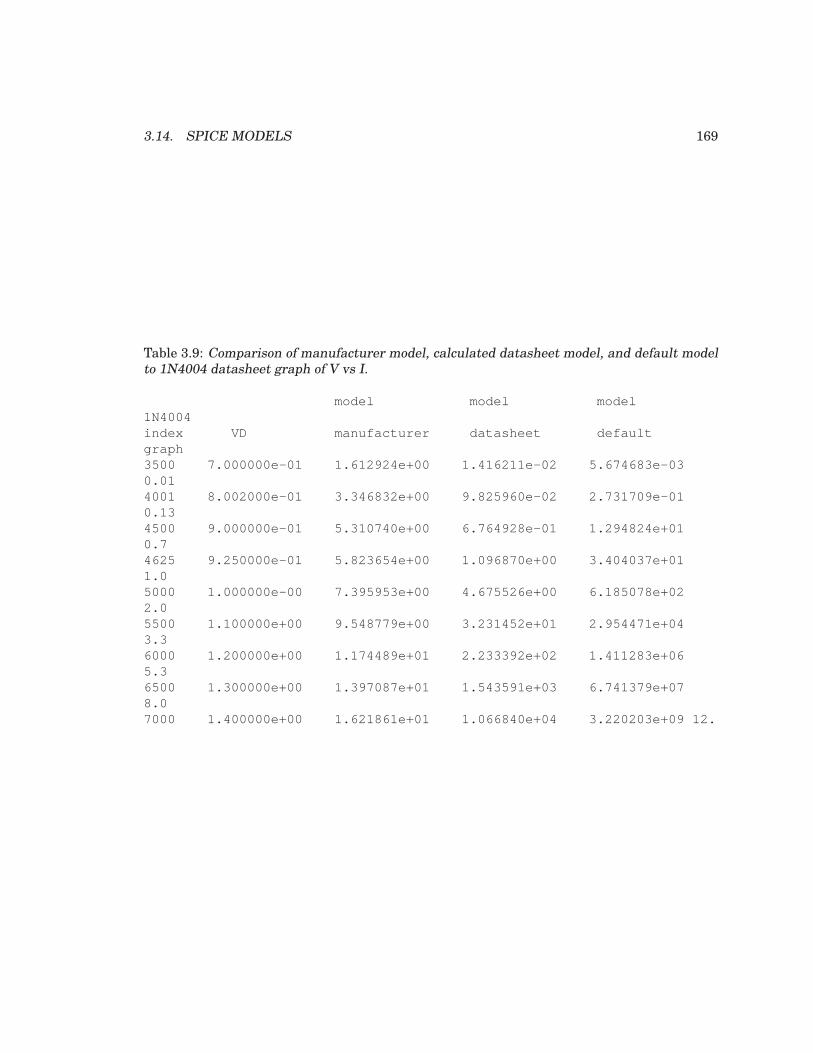
3.14. SPICE MODELS 169
Table 3.9: Comparison of manufacturer model, calculated datasheet model, and default modelto 1N4004 datasheet graph of V vs I.
model model model1N4004index VD manufacturer datasheet defaultgraph3500 7.000000e-01 1.612924e+00 1.416211e-02 5.674683e-0 30.014001 8.002000e-01 3.346832e+00 9.825960e-02 2.731709e-0 10.134500 9.000000e-01 5.310740e+00 6.764928e-01 1.294824e+0 10.74625 9.250000e-01 5.823654e+00 1.096870e+00 3.404037e+0 11.05000 1.000000e-00 7.395953e+00 4.675526e+00 6.185078e+0 22.05500 1.100000e+00 9.548779e+00 3.231452e+01 2.954471e+0 43.36000 1.200000e+00 1.174489e+01 2.233392e+02 1.411283e+0 65.36500 1.300000e+00 1.397087e+01 1.543591e+03 6.741379e+0 78.07000 1.400000e+00 1.621861e+01 1.066840e+04 3.220203e+0 9 12.
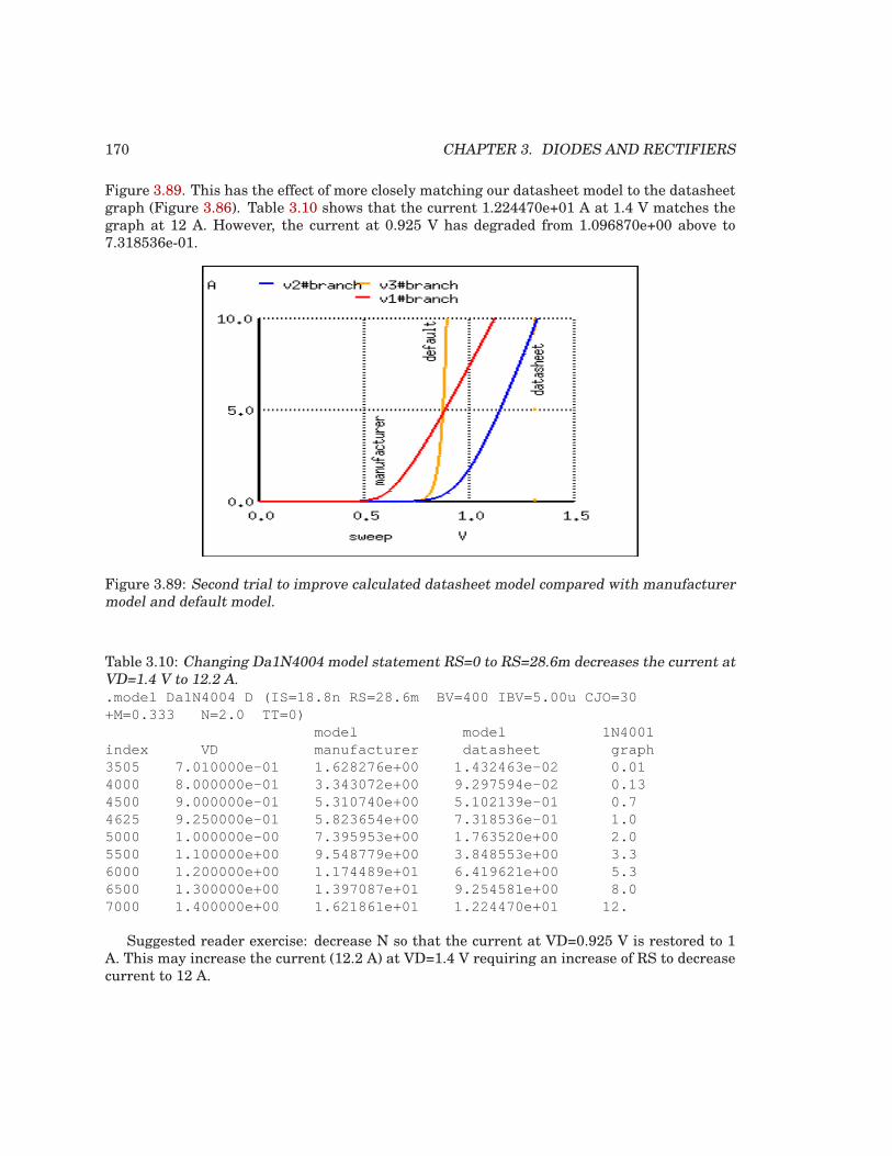
170 CHAPTER 3. DIODES AND RECTIFIERS
Figure 3.89. This has the effect of more closely matching our datasheet model to the datasheetgraph (Figure 3.86). Table 3.10 shows that the current 1.224470e+01 A at 1.4 V matches thegraph at 12 A. However, the current at 0.925 V has degraded from 1.096870e+00 above to7.318536e-01.
Figure 3.89: Second trial to improve calculated datasheet model compared with manufacturermodel and default model.
Table 3.10: Changing Da1N4004 model statement RS=0 to RS=28.6m decreases the current atVD=1.4 V to 12.2 A..model Da1N4004 D (IS=18.8n RS=28.6m BV=400 IBV=5.00u CJO= 30+M=0.333 N=2.0 TT=0)
model model 1N4001index VD manufacturer datasheet graph3505 7.010000e-01 1.628276e+00 1.432463e-02 0.014000 8.000000e-01 3.343072e+00 9.297594e-02 0.134500 9.000000e-01 5.310740e+00 5.102139e-01 0.74625 9.250000e-01 5.823654e+00 7.318536e-01 1.05000 1.000000e-00 7.395953e+00 1.763520e+00 2.05500 1.100000e+00 9.548779e+00 3.848553e+00 3.36000 1.200000e+00 1.174489e+01 6.419621e+00 5.36500 1.300000e+00 1.397087e+01 9.254581e+00 8.07000 1.400000e+00 1.621861e+01 1.224470e+01 12.
Suggested reader exercise: decrease N so that the current at VD=0.925 V is restored to 1A. This may increase the current (12.2 A) at VD=1.4 V requiring an increase of RS to decreasecurrent to 12 A.
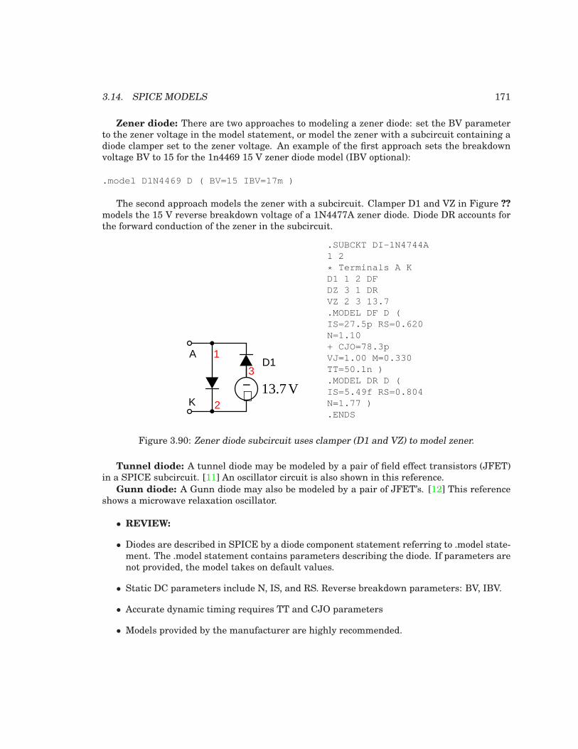
3.14. SPICE MODELS 171
Zener diode: There are two approaches to modeling a zener diode: set the BV parameterto the zener voltage in the model statement, or model the zener with a subcircuit containing adiode clamper set to the zener voltage. An example of the first approach sets the breakdownvoltage BV to 15 for the 1n4469 15 V zener diode model (IBV optional):
.model D1N4469 D ( BV=15 IBV=17m )
The second approach models the zener with a subcircuit. Clamper D1 and VZ in Figure ??
models the 15 V reverse breakdown voltage of a 1N4477A zener diode. Diode DR accounts forthe forward conduction of the zener in the subcircuit.
+−
13.7V
1
3
2
A
K
D1
.SUBCKT DI-1N4744A1 2
* Terminals A KD1 1 2 DFDZ 3 1 DRVZ 2 3 13.7.MODEL DF D (IS=27.5p RS=0.620N=1.10+ CJO=78.3pVJ=1.00 M=0.330TT=50.1n ).MODEL DR D (IS=5.49f RS=0.804N=1.77 ).ENDS
Figure 3.90: Zener diode subcircuit uses clamper (D1 and VZ) to model zener.
Tunnel diode: A tunnel diode may be modeled by a pair of field effect transistors (JFET)in a SPICE subcircuit. [11] An oscillator circuit is also shown in this reference.
Gunn diode: A Gunn diode may also be modeled by a pair of JFET’s. [12] This referenceshows a microwave relaxation oscillator.
• REVIEW:
• Diodes are described in SPICE by a diode component statement referring to .model state-ment. The .model statement contains parameters describing the diode. If parameters arenot provided, the model takes on default values.
• Static DC parameters include N, IS, and RS. Reverse breakdown parameters: BV, IBV.
• Accurate dynamic timing requires TT and CJO parameters
• Models provided by the manufacturer are highly recommended.
172 CHAPTER 3. DIODES AND RECTIFIERS
Contributors
Contributors to this chapter are listed in chronological order of their contributions, from mostrecent to first. See Appendix 2 (Contributor List) for dates and contact information.
Jered Wierzbicki (December 2002): Pointed out error in diode equation – Boltzmann’sconstant shown incorrectly.
Bibliography
[1] Paolo Antognetti, Giuseppe Massobrio “Semiconductor Device Modeling with SPICE,”ISBN 0-07-002107-4, 1988
[2] ATCO Newsletter, Volume 14 No. 1, January 1997 athttp://www.atco.tv/homepage/vol14 1.pdf
[3] D.A. Brunner, et al,, “A Cockcroft-Walton Base for the FEU84-3 Photomultiplier Tube,”Department of Physics, Indiana University, Bloomington, Indiana 47405 January 1998,at http://dustbunny.physics.indiana.edu/˜paul/cwbase/
[4] Brenton Burnet, “The Basic Physics and Design of III-V Multijunction Solar,” NREL, atphotochemistry.epfl.ch/EDEY/NREL.pdf
[5] Diodes Incorporated http://www.diodes.com/products/spicemodels/index.ph p
[6] Diodes Incorporated, “1N4001/L - 1N4007/l, 1.0A rectifier,” athttp://www.diodes.com/datasheets/ds28002.pdf
[7] “Solar firm gains $30 million in funding,” EE Times, 07/12/2007 athttp://www.eetimes.com/news/latest/showArticle.jhtm l?articleID=201001129
[8] Christiana Honsberg, Stuart Bowden, “Photovoltaics CDROM,” athttp://www.udel.edu/igert/pvcdrom/
[9] R. R. King, et. al., “40% efficient metamorphic GaInP/GaInAs/Ge mul-tijunction solar cells”, Applied Physics Letters, 90, 183516 (2007) , athttp://scitation.aip.org/getabs/servlet/GetabsServl et?prog=normal&id=APPLAB000090000018183516000001&idtype=cvips&gifs =yes
[10] Kim W Mitchell, “Method of making a thin film cadmium telluride solar cell,” UnitedStates Patent 4734381,http://www.freepatentsonline.com/4734381.html
[11] Karl H. Muller “RF/Microwave Analysis” Intusoft Newsletter #51, November 1997, athttp://www.intusoft.com/nlhtm/nl51.htm
[12] “A Gunn Diode Relaxation Oscillator,” Intusoft Newsletter #52, February 1998, athttp://www.intusoft.com/nlhtm/nl52.htm
[13] OAK Solar., “Technical LED’s LED color chart,” athttp://www.oksolar.com/led/led color chart.htm
BIBLIOGRAPHY 173
[14] Ian Poole, “Summary of the Gunn Diode,” at http://www.radio-electronics.com/nfo/data/semicond/gunndiode/gunndiode.php
[15] Muhammad H. Rashid, “SPICE for Power Electronics and Electric Power,” ISBN 0-13-030420-4, 1993
[16] “SPICE model index,” V2.16 30-Nov-05, at http://homepages.which.net/˜paul.hills/Circuits/Spice/ModelIndex.html
[17] Neil Thomas, “Advancing CIGS Solar Cell Manufacturing Technology,” April 6, 2007 athttp://www.renewableenergyaccess.com/rea/news/story ?id=48033&src=rss
[18] P.J. Verlinden, Sinton, K. Wickham, R.M. Swanson Crane, “BACKSIDE-CONTACT SILICON SOLAR CELLS WITH IMPROVED EFFICIENCY.” athttp://www.sunpowercorp.com/techpapers/EPSEC97.pdf
[19] Christian Wolff, “Radar Principles,” Radar components, Gunn diodes at athttp://www.radartutorial.eu/17.bauteile/bt12.en.htm
[20] L. Yuan, M. R. Melloch, J. A. Cooper, K. J. Webb,“Silicon Carbide IM-PATT Oscillators for High-Power Microwave and Millimeter-Wave Gen-eration,” IEEE/Cornell Conference on Advanced Concepts in High SpeedSemiconductor Devices and Circuits, Ithaca, NY, August 7-9, 2000. athttp://www.ecn.purdue.edu/WBG/Device Research/IMPATT Diodes/Index.html
[21] Alan Seabaugh, Zhaoming HU, Qingmin LIU, David Rink, JinliWang, “Silicon Based Tunnel Diodes and Integrated Circuits,” athttp://www.nd.edu/˜nano/0a1003QFDpaper v1.pdf
[22] S. M. Sze, G. Gibbons, “Avalanche breakdown voltages of abrupt and linearly graded p-njunctions in Ge, Si, GaAs, and Ga P,” Appl. Phys. Lett., 8, 111 (1966).
[23] Lisa Zyga, “40% efficient solar cells to be used for solar electricity”, PhysOrgForum, athttp://www.physorg.com/news99904887.html

174 CHAPTER 3. DIODES AND RECTIFIERS

Chapter 4
BIPOLAR JUNCTION
TRANSISTORS
Contents
4.1 Introduction . . . . . . . . . . . . . . . . . . . . . . . . . . . . . . . . . . . . . . 176
4.2 The transistor as a switch . . . . . . . . . . . . . . . . . . . . . . . . . . . . . 178
4.3 Meter check of a transistor . . . . . . . . . . . . . . . . . . . . . . . . . . . . . 181
4.4 Active mode operation . . . . . . . . . . . . . . . . . . . . . . . . . . . . . . . 185
4.5 The common-emitter amplifier . . . . . . . . . . . . . . . . . . . . . . . . . . 191
4.6 The common-collector amplifier . . . . . . . . . . . . . . . . . . . . . . . . . 204
4.7 The common-base amplifier . . . . . . . . . . . . . . . . . . . . . . . . . . . . 212
4.8 The cascode amplifier . . . . . . . . . . . . . . . . . . . . . . . . . . . . . . . . 220
4.9 Biasing techniques . . . . . . . . . . . . . . . . . . . . . . . . . . . . . . . . . . 224
4.10 Biasing calculations . . . . . . . . . . . . . . . . . . . . . . . . . . . . . . . . . 237
4.10.1 Base Bias . . . . . . . . . . . . . . . . . . . . . . . . . . . . . . . . . . . . . 237
4.10.2 Collector-feedback bias . . . . . . . . . . . . . . . . . . . . . . . . . . . . . 238
4.10.3 Emitter-bias . . . . . . . . . . . . . . . . . . . . . . . . . . . . . . . . . . . 239
4.10.4 Voltage divider bias . . . . . . . . . . . . . . . . . . . . . . . . . . . . . . 245
4.11 Input and output coupling . . . . . . . . . . . . . . . . . . . . . . . . . . . . . 249
4.12 Feedback . . . . . . . . . . . . . . . . . . . . . . . . . . . . . . . . . . . . . . . . 258
4.13 Amplifier impedances . . . . . . . . . . . . . . . . . . . . . . . . . . . . . . . . 265
4.14 Current mirrors . . . . . . . . . . . . . . . . . . . . . . . . . . . . . . . . . . . . 266
4.15 Transistor ratings and packages . . . . . . . . . . . . . . . . . . . . . . . . . 271
4.16 BJT quirks . . . . . . . . . . . . . . . . . . . . . . . . . . . . . . . . . . . . . . . 273
4.16.1 Nonlinearity . . . . . . . . . . . . . . . . . . . . . . . . . . . . . . . . . . . 274
4.16.2 Temperature drift . . . . . . . . . . . . . . . . . . . . . . . . . . . . . . . . 274
4.16.3 Thermal runaway . . . . . . . . . . . . . . . . . . . . . . . . . . . . . . . . 276
4.16.4 Junction capacitance . . . . . . . . . . . . . . . . . . . . . . . . . . . . . . 276
4.16.5 Noise . . . . . . . . . . . . . . . . . . . . . . . . . . . . . . . . . . . . . . . 277
175
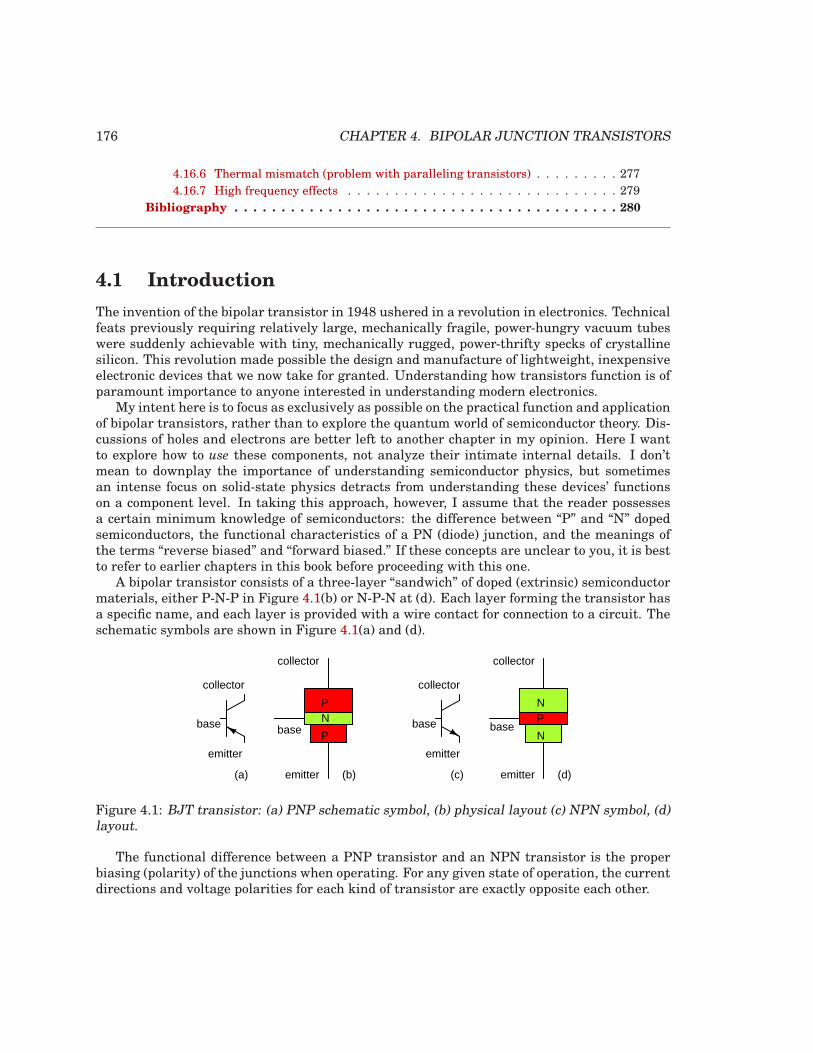
176 CHAPTER 4. BIPOLAR JUNCTION TRANSISTORS
4.16.6 Thermal mismatch (problem with paralleling transistors) . . . . . . . . . 277
4.16.7 High frequency effects . . . . . . . . . . . . . . . . . . . . . . . . . . . . . 279
Bibliography . . . . . . . . . . . . . . . . . . . . . . . . . . . . . . . . . . . . . . . . . 280
4.1 Introduction
The invention of the bipolar transistor in 1948 ushered in a revolution in electronics. Technicalfeats previously requiring relatively large, mechanically fragile, power-hungry vacuum tubeswere suddenly achievable with tiny, mechanically rugged, power-thrifty specks of crystallinesilicon. This revolution made possible the design and manufacture of lightweight, inexpensiveelectronic devices that we now take for granted. Understanding how transistors function is ofparamount importance to anyone interested in understanding modern electronics.
My intent here is to focus as exclusively as possible on the practical function and applicationof bipolar transistors, rather than to explore the quantum world of semiconductor theory. Dis-cussions of holes and electrons are better left to another chapter in my opinion. Here I wantto explore how to use these components, not analyze their intimate internal details. I don’tmean to downplay the importance of understanding semiconductor physics, but sometimesan intense focus on solid-state physics detracts from understanding these devices’ functionson a component level. In taking this approach, however, I assume that the reader possessesa certain minimum knowledge of semiconductors: the difference between “P” and “N” dopedsemiconductors, the functional characteristics of a PN (diode) junction, and the meanings ofthe terms “reverse biased” and “forward biased.” If these concepts are unclear to you, it is bestto refer to earlier chapters in this book before proceeding with this one.
A bipolar transistor consists of a three-layer “sandwich” of doped (extrinsic) semiconductormaterials, either P-N-P in Figure 4.1(b) or N-P-N at (d). Each layer forming the transistor hasa specific name, and each layer is provided with a wire contact for connection to a circuit. Theschematic symbols are shown in Figure 4.1(a) and (d).
emitter
base
collector
base
emitter
collector
base
emitter
collector
NP
emitter
base
collector
N
NP
P
(a) (b) (c) (d)
Figure 4.1: BJT transistor: (a) PNP schematic symbol, (b) physical layout (c) NPN symbol, (d)layout.
The functional difference between a PNP transistor and an NPN transistor is the properbiasing (polarity) of the junctions when operating. For any given state of operation, the currentdirections and voltage polarities for each kind of transistor are exactly opposite each other.
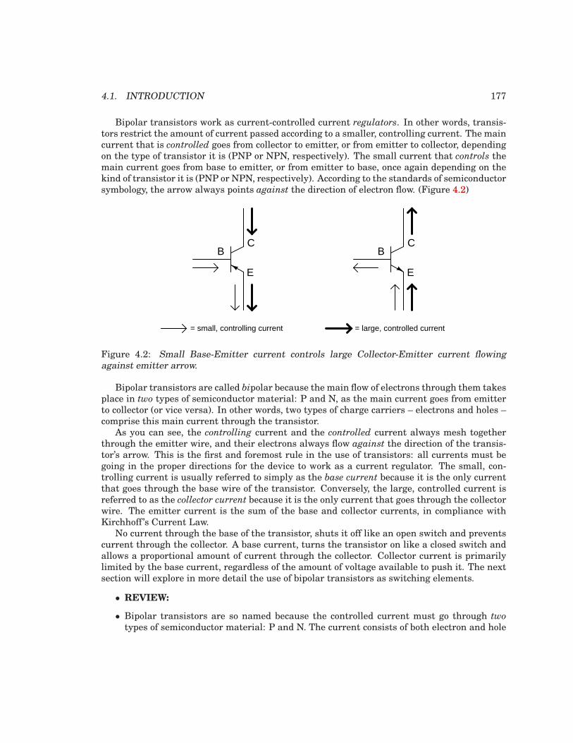
4.1. INTRODUCTION 177
Bipolar transistors work as current-controlled current regulators. In other words, transis-tors restrict the amount of current passed according to a smaller, controlling current. The maincurrent that is controlled goes from collector to emitter, or from emitter to collector, dependingon the type of transistor it is (PNP or NPN, respectively). The small current that controls themain current goes from base to emitter, or from emitter to base, once again depending on thekind of transistor it is (PNP or NPN, respectively). According to the standards of semiconductorsymbology, the arrow always points against the direction of electron flow. (Figure 4.2)
CB
E
CB
E
= small, controlling current = large, controlled current
Figure 4.2: Small Base-Emitter current controls large Collector-Emitter current flowingagainst emitter arrow.
Bipolar transistors are called bipolar because the main flow of electrons through them takesplace in two types of semiconductor material: P and N, as the main current goes from emitterto collector (or vice versa). In other words, two types of charge carriers – electrons and holes –comprise this main current through the transistor.
As you can see, the controlling current and the controlled current always mesh togetherthrough the emitter wire, and their electrons always flow against the direction of the transis-tor’s arrow. This is the first and foremost rule in the use of transistors: all currents must begoing in the proper directions for the device to work as a current regulator. The small, con-trolling current is usually referred to simply as the base current because it is the only currentthat goes through the base wire of the transistor. Conversely, the large, controlled current isreferred to as the collector current because it is the only current that goes through the collectorwire. The emitter current is the sum of the base and collector currents, in compliance withKirchhoff ’s Current Law.
No current through the base of the transistor, shuts it off like an open switch and preventscurrent through the collector. A base current, turns the transistor on like a closed switch andallows a proportional amount of current through the collector. Collector current is primarilylimited by the base current, regardless of the amount of voltage available to push it. The nextsection will explore in more detail the use of bipolar transistors as switching elements.
• REVIEW:
• Bipolar transistors are so named because the controlled current must go through two
types of semiconductor material: P and N. The current consists of both electron and hole
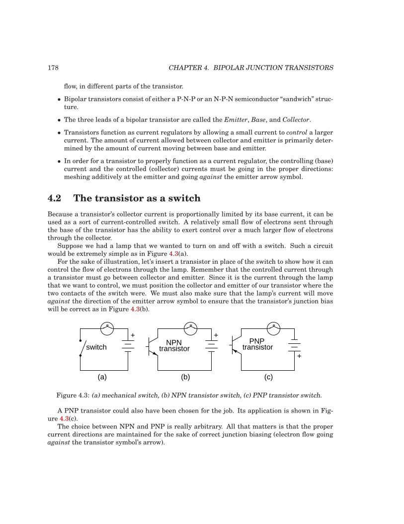
178 CHAPTER 4. BIPOLAR JUNCTION TRANSISTORS
flow, in different parts of the transistor.
• Bipolar transistors consist of either a P-N-P or an N-P-N semiconductor “sandwich” struc-ture.
• The three leads of a bipolar transistor are called the Emitter, Base, and Collector.
• Transistors function as current regulators by allowing a small current to control a largercurrent. The amount of current allowed between collector and emitter is primarily deter-mined by the amount of current moving between base and emitter.
• In order for a transistor to properly function as a current regulator, the controlling (base)current and the controlled (collector) currents must be going in the proper directions:meshing additively at the emitter and going against the emitter arrow symbol.
4.2 The transistor as a switch
Because a transistor’s collector current is proportionally limited by its base current, it can beused as a sort of current-controlled switch. A relatively small flow of electrons sent throughthe base of the transistor has the ability to exert control over a much larger flow of electronsthrough the collector.
Suppose we had a lamp that we wanted to turn on and off with a switch. Such a circuitwould be extremely simple as in Figure 4.3(a).
For the sake of illustration, let’s insert a transistor in place of the switch to show how it cancontrol the flow of electrons through the lamp. Remember that the controlled current througha transistor must go between collector and emitter. Since it is the current through the lampthat we want to control, we must position the collector and emitter of our transistor where thetwo contacts of the switch were. We must also make sure that the lamp’s current will moveagainst the direction of the emitter arrow symbol to ensure that the transistor’s junction biaswill be correct as in Figure 4.3(b).
transistorNPN
transistorPNP
switch
(a) (b) (c)
+ +
+
Figure 4.3: (a) mechanical switch, (b) NPN transistor switch, (c) PNP transistor switch.
A PNP transistor could also have been chosen for the job. Its application is shown in Fig-ure 4.3(c).
The choice between NPN and PNP is really arbitrary. All that matters is that the propercurrent directions are maintained for the sake of correct junction biasing (electron flow goingagainst the transistor symbol’s arrow).
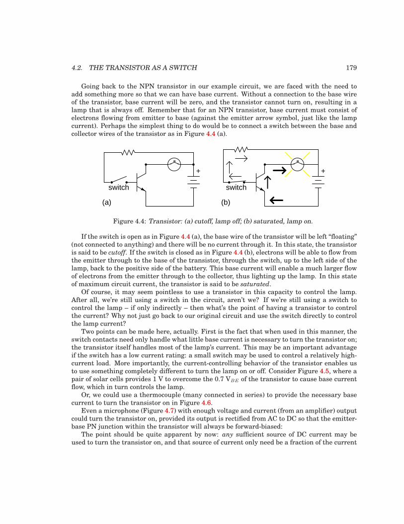
4.2. THE TRANSISTOR AS A SWITCH 179
Going back to the NPN transistor in our example circuit, we are faced with the need toadd something more so that we can have base current. Without a connection to the base wireof the transistor, base current will be zero, and the transistor cannot turn on, resulting in alamp that is always off. Remember that for an NPN transistor, base current must consist ofelectrons flowing from emitter to base (against the emitter arrow symbol, just like the lampcurrent). Perhaps the simplest thing to do would be to connect a switch between the base andcollector wires of the transistor as in Figure 4.4 (a).
switchswitch
++
(a) (b)
Figure 4.4: Transistor: (a) cutoff, lamp off; (b) saturated, lamp on.
If the switch is open as in Figure 4.4 (a), the base wire of the transistor will be left “floating”(not connected to anything) and there will be no current through it. In this state, the transistoris said to be cutoff. If the switch is closed as in Figure 4.4 (b), electrons will be able to flow fromthe emitter through to the base of the transistor, through the switch, up to the left side of thelamp, back to the positive side of the battery. This base current will enable a much larger flowof electrons from the emitter through to the collector, thus lighting up the lamp. In this stateof maximum circuit current, the transistor is said to be saturated.
Of course, it may seem pointless to use a transistor in this capacity to control the lamp.After all, we’re still using a switch in the circuit, aren’t we? If we’re still using a switch tocontrol the lamp – if only indirectly – then what’s the point of having a transistor to controlthe current? Why not just go back to our original circuit and use the switch directly to controlthe lamp current?
Two points can be made here, actually. First is the fact that when used in this manner, theswitch contacts need only handle what little base current is necessary to turn the transistor on;the transistor itself handles most of the lamp’s current. This may be an important advantageif the switch has a low current rating: a small switch may be used to control a relatively high-current load. More importantly, the current-controlling behavior of the transistor enables usto use something completely different to turn the lamp on or off. Consider Figure 4.5, where apair of solar cells provides 1 V to overcome the 0.7 VBE of the transistor to cause base currentflow, which in turn controls the lamp.
Or, we could use a thermocouple (many connected in series) to provide the necessary basecurrent to turn the transistor on in Figure 4.6.
Even a microphone (Figure 4.7) with enough voltage and current (from an amplifier) outputcould turn the transistor on, provided its output is rectified from AC to DC so that the emitter-base PN junction within the transistor will always be forward-biased:
The point should be quite apparent by now: any sufficient source of DC current may beused to turn the transistor on, and that source of current only need be a fraction of the current
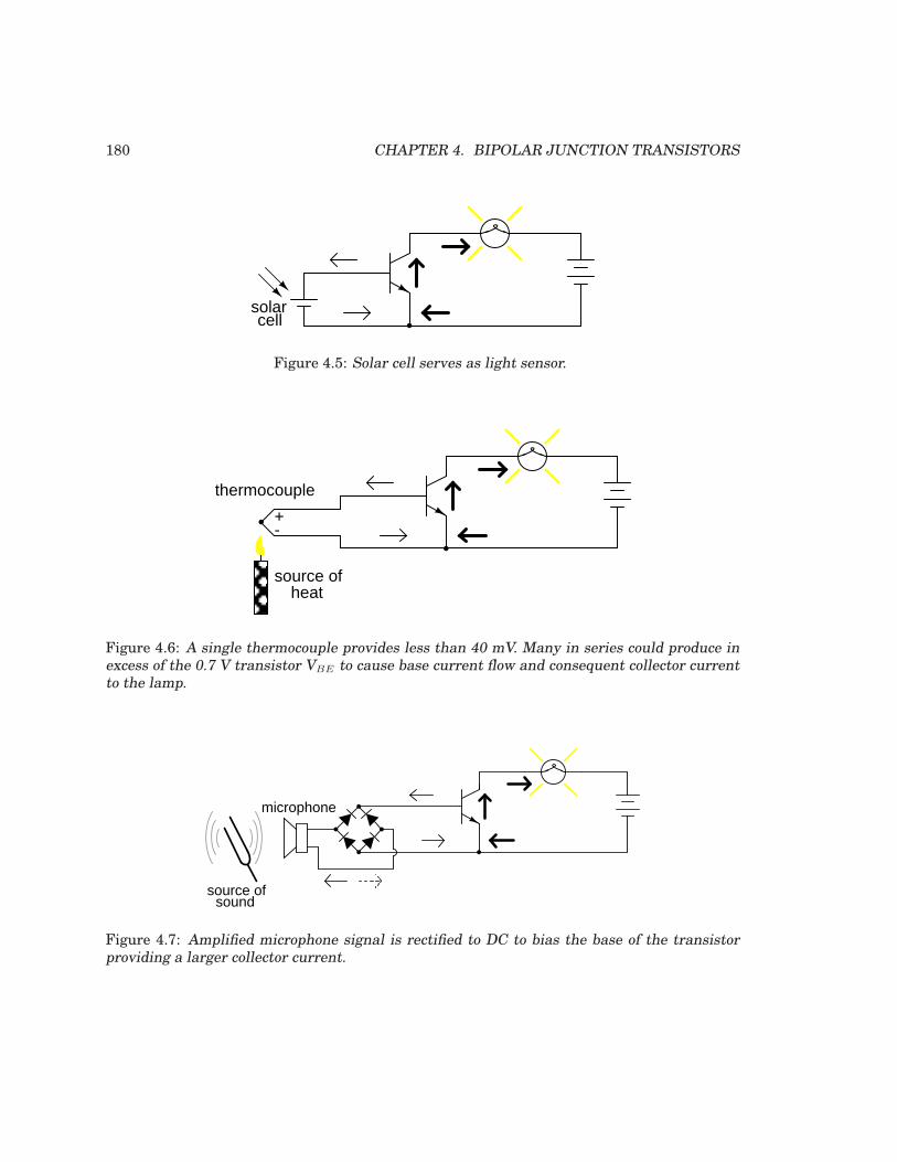
180 CHAPTER 4. BIPOLAR JUNCTION TRANSISTORS
solarcell
Figure 4.5: Solar cell serves as light sensor.
+-
thermocouple
source ofheat
Figure 4.6: A single thermocouple provides less than 40 mV. Many in series could produce inexcess of the 0.7 V transistor VBE to cause base current flow and consequent collector currentto the lamp.
microphone
source ofsound
Figure 4.7: Amplified microphone signal is rectified to DC to bias the base of the transistorproviding a larger collector current.
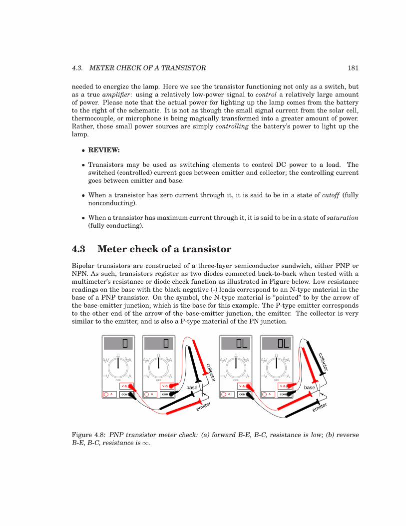
4.3. METER CHECK OF A TRANSISTOR 181
needed to energize the lamp. Here we see the transistor functioning not only as a switch, butas a true amplifier: using a relatively low-power signal to control a relatively large amountof power. Please note that the actual power for lighting up the lamp comes from the batteryto the right of the schematic. It is not as though the small signal current from the solar cell,thermocouple, or microphone is being magically transformed into a greater amount of power.Rather, those small power sources are simply controlling the battery’s power to light up thelamp.
• REVIEW:
• Transistors may be used as switching elements to control DC power to a load. Theswitched (controlled) current goes between emitter and collector; the controlling currentgoes between emitter and base.
• When a transistor has zero current through it, it is said to be in a state of cutoff (fullynonconducting).
• When a transistor has maximum current through it, it is said to be in a state of saturation(fully conducting).
4.3 Meter check of a transistor
Bipolar transistors are constructed of a three-layer semiconductor sandwich, either PNP orNPN. As such, transistors register as two diodes connected back-to-back when tested with amultimeter’s resistance or diode check function as illustrated in Figure below. Low resistancereadings on the base with the black negative (-) leads correspond to an N-type material in thebase of a PNP transistor. On the symbol, the N-type material is ”pointed” to by the arrow ofthe base-emitter junction, which is the base for this example. The P-type emitter correspondsto the other end of the arrow of the base-emitter junction, the emitter. The collector is verysimilar to the emitter, and is also a P-type material of the PN junction.
base
emitter
collector
COMA
V
V A
AOFF
COMA
V
V A
AOFF
baseCOMA
V
V A
AOFF
COMA
V
V A
AOFF
emitter
collector
Figure 4.8: PNP transistor meter check: (a) forward B-E, B-C, resistance is low; (b) reverseB-E, B-C, resistance is ∞.
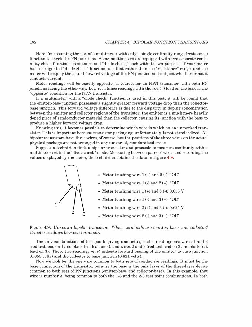
182 CHAPTER 4. BIPOLAR JUNCTION TRANSISTORS
Here I’m assuming the use of a multimeter with only a single continuity range (resistance)function to check the PN junctions. Some multimeters are equipped with two separate conti-nuity check functions: resistance and “diode check,” each with its own purpose. If your meterhas a designated “diode check” function, use that rather than the “resistance” range, and themeter will display the actual forward voltage of the PN junction and not just whether or not itconducts current.
Meter readings will be exactly opposite, of course, for an NPN transistor, with both PNjunctions facing the other way. Low resistance readings with the red (+) lead on the base is the“opposite” condition for the NPN transistor.
If a multimeter with a “diode check” function is used in this test, it will be found thatthe emitter-base junction possesses a slightly greater forward voltage drop than the collector-base junction. This forward voltage difference is due to the disparity in doping concentrationbetween the emitter and collector regions of the transistor: the emitter is a much more heavilydoped piece of semiconductor material than the collector, causing its junction with the base toproduce a higher forward voltage drop.
Knowing this, it becomes possible to determine which wire is which on an unmarked tran-sistor. This is important because transistor packaging, unfortunately, is not standardized. Allbipolar transistors have three wires, of course, but the positions of the three wires on the actualphysical package are not arranged in any universal, standardized order.
Suppose a technician finds a bipolar transistor and proceeds to measure continuity with amultimeter set in the “diode check” mode. Measuring between pairs of wires and recording thevalues displayed by the meter, the technician obtains the data in Figure 4.9.
1
2 3
• Meter touching wire 1 (+) and 2 (-): “OL”
• Meter touching wire 1 (-) and 2 (+): “OL”
• Meter touching wire 1 (+) and 3 (-): 0.655 V
• Meter touching wire 1 (-) and 3 (+): “OL”
• Meter touching wire 2 (+) and 3 (-): 0.621 V
• Meter touching wire 2 (-) and 3 (+): “OL”
Figure 4.9: Unknown bipolar transistor. Which terminals are emitter, base, and collector?Ω-meter readings between terminals.
The only combinations of test points giving conducting meter readings are wires 1 and 3(red test lead on 1 and black test lead on 3), and wires 2 and 3 (red test lead on 2 and black testlead on 3). These two readings must indicate forward biasing of the emitter-to-base junction(0.655 volts) and the collector-to-base junction (0.621 volts).
Now we look for the one wire common to both sets of conductive readings. It must be thebase connection of the transistor, because the base is the only layer of the three-layer devicecommon to both sets of PN junctions (emitter-base and collector-base). In this example, thatwire is number 3, being common to both the 1-3 and the 2-3 test point combinations. In both
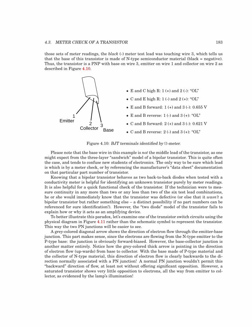
4.3. METER CHECK OF A TRANSISTOR 183
those sets of meter readings, the black (-) meter test lead was touching wire 3, which tells usthat the base of this transistor is made of N-type semiconductor material (black = negative).Thus, the transistor is a PNP with base on wire 3, emitter on wire 1 and collector on wire 2 asdescribed in Figure 4.10.
1
2 3Base
Emitter
Collector
• E and C high R: 1 (+) and 2 (-): “OL”
• C and E high R: 1 (-) and 2 (+): “OL”
• E and B forward: 1 (+) and 3 (-): 0.655 V
• E and B reverse: 1 (-) and 3 (+): “OL”
• C and B forward: 2 (+) and 3 (-): 0.621 V
• C and B reverse: 2 (-) and 3 (+): “OL”
Figure 4.10: BJT terminals identified by Ω-meter.
Please note that the base wire in this example is not the middle lead of the transistor, as onemight expect from the three-layer “sandwich” model of a bipolar transistor. This is quite oftenthe case, and tends to confuse new students of electronics. The only way to be sure which leadis which is by a meter check, or by referencing the manufacturer’s “data sheet” documentationon that particular part number of transistor.
Knowing that a bipolar transistor behaves as two back-to-back diodes when tested with aconductivity meter is helpful for identifying an unknown transistor purely by meter readings.It is also helpful for a quick functional check of the transistor. If the technician were to mea-sure continuity in any more than two or any less than two of the six test lead combinations,he or she would immediately know that the transistor was defective (or else that it wasn’t abipolar transistor but rather something else – a distinct possibility if no part numbers can bereferenced for sure identification!). However, the “two diode” model of the transistor fails toexplain how or why it acts as an amplifying device.
To better illustrate this paradox, let’s examine one of the transistor switch circuits using thephysical diagram in Figure 4.11 rather than the schematic symbol to represent the transistor.This way the two PN junctions will be easier to see.
A grey-colored diagonal arrow shows the direction of electron flow through the emitter-basejunction. This part makes sense, since the electrons are flowing from the N-type emitter to theP-type base: the junction is obviously forward-biased. However, the base-collector junction isanother matter entirely. Notice how the grey-colored thick arrow is pointing in the directionof electron flow (up-wards) from base to collector. With the base made of P-type material andthe collector of N-type material, this direction of electron flow is clearly backwards to the di-rection normally associated with a PN junction! A normal PN junction wouldn’t permit this“backward” direction of flow, at least not without offering significant opposition. However, asaturated transistor shows very little opposition to electrons, all the way from emitter to col-lector, as evidenced by the lamp’s illumination!
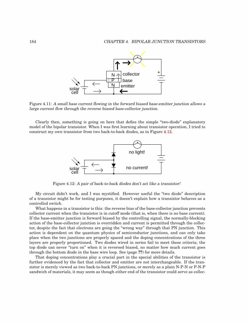
184 CHAPTER 4. BIPOLAR JUNCTION TRANSISTORS
NP
emitterbasecollector
Nsolarcell
+
Figure 4.11: A small base current flowing in the forward biased base-emitter junction allows alarge current flow through the reverse biased base-collector junction.
Clearly then, something is going on here that defies the simple “two-diode” explanatorymodel of the bipolar transistor. When I was first learning about transistor operation, I tried toconstruct my own transistor from two back-to-back diodes, as in Figure 4.12.
solarcell
no light!
no current!
Figure 4.12: A pair of back-to-back diodes don’t act like a transistor!
My circuit didn’t work, and I was mystified. However useful the “two diode” descriptionof a transistor might be for testing purposes, it doesn’t explain how a transistor behaves as acontrolled switch.
What happens in a transistor is this: the reverse bias of the base-collector junction preventscollector current when the transistor is in cutoff mode (that is, when there is no base current).If the base-emitter junction is forward biased by the controlling signal, the normally-blockingaction of the base-collector junction is overridden and current is permitted through the collec-tor, despite the fact that electrons are going the “wrong way” through that PN junction. Thisaction is dependent on the quantum physics of semiconductor junctions, and can only takeplace when the two junctions are properly spaced and the doping concentrations of the threelayers are properly proportioned. Two diodes wired in series fail to meet these criteria; thetop diode can never “turn on” when it is reversed biased, no matter how much current goesthrough the bottom diode in the base wire loop. See (page ??) for more details.
That doping concentrations play a crucial part in the special abilities of the transistor isfurther evidenced by the fact that collector and emitter are not interchangeable. If the tran-sistor is merely viewed as two back-to-back PN junctions, or merely as a plain N-P-N or P-N-Psandwich of materials, it may seem as though either end of the transistor could serve as collec-
4.4. ACTIVE MODE OPERATION 185
tor or emitter. This, however, is not true. If connected “backwards” in a circuit, a base-collectorcurrent will fail to control current between collector and emitter. Despite the fact that both theemitter and collector layers of a bipolar transistor are of the same doping type (either N or P),collector and emitter are definitely not identical!
Current through the emitter-base junction allows current through the reverse-biased base-collector junction. The action of base current can be thought of as “opening a gate” for currentthrough the collector. More specifically, any given amount of emitter-to-base current permits a
limited amount of base-to-collector current. For every electron that passes through the emitter-base junction and on through the base wire, a certain, number of electrons pass through thebase-collector junction and no more.
In the next section, this current-limiting of the transistor will be investigated in more detail.
• REVIEW:
• Tested with a multimeter in the “resistance” or “diode check” modes, a transistor behaveslike two back-to-back PN (diode) junctions.
• The emitter-base PN junction has a slightly greater forward voltage drop than the collector-base PN junction, because of heavier doping of the emitter semiconductor layer.
• The reverse-biased base-collector junction normally blocks any current from going throughthe transistor between emitter and collector. However, that junction begins to conduct ifcurrent is drawn through the base wire. Base current may be thought of as “opening agate” for a certain, limited amount of current through the collector.
4.4 Active mode operation
When a transistor is in the fully-off state (like an open switch), it is said to be cutoff. Con-versely, when it is fully conductive between emitter and collector (passing as much currentthrough the collector as the collector power supply and load will allow), it is said to be sat-
urated. These are the two modes of operation explored thus far in using the transistor as aswitch.
However, bipolar transistors don’t have to be restricted to these two extreme modes of oper-ation. As we learned in the previous section, base current “opens a gate” for a limited amountof current through the collector. If this limit for the controlled current is greater than zerobut less than the maximum allowed by the power supply and load circuit, the transistor will“throttle” the collector current in a mode somewhere between cutoff and saturation. This modeof operation is called the active mode.
An automotive analogy for transistor operation is as follows: cutoff is the condition of nomotive force generated by the mechanical parts of the car to make it move. In cutoff mode, thebrake is engaged (zero base current), preventing motion (collector current). Active mode is theautomobile cruising at a constant, controlled speed (constant, controlled collector current) asdictated by the driver. Saturation the automobile driving up a steep hill that prevents it fromgoing as fast as the driver wishes. In other words, a “saturated” automobile is one with theaccelerator pedal pushed all the way down (base current calling for more collector current thancan be provided by the power supply/load circuit).
186 CHAPTER 4. BIPOLAR JUNCTION TRANSISTORS
Let’s set up a circuit for SPICE simulation to demonstrate what happens when a transistoris in its active mode of operation. (Figure 4.13)
V1
I1
Q1
Vammeter
0 V
1
0 0 0
2 3
Current source
bipolar transistorsimulationi1 0 1 dc 20uq1 2 1 0 mod1vammeter 3 2 dc 0v1 3 0 dc.model mod1 npn.dc v1 0 2 0.05.plot dci(vammeter).end
Figure 4.13: Circuit for “active mode” SPICE simulation, and netlist.
“Q” is the standard letter designation for a transistor in a schematic diagram, just as “R”is for resistor and “C” is for capacitor. In this circuit, we have an NPN transistor poweredby a battery (V1) and controlled by current through a current source (I1). A current sourceis a device that outputs a specific amount of current, generating as much or as little voltageacross its terminals to ensure that exact amount of current through it. Current sources arenotoriously difficult to find in nature (unlike voltage sources, which by contrast attempt tomaintain a constant voltage, outputting as much or as little current in the fulfillment of thattask), but can be simulated with a small collection of electronic components. As we are aboutto see, transistors themselves tend to mimic the constant-current behavior of a current sourcein their ability to regulate current at a fixed value.
In the SPICE simulation, we’ll set the current source at a constant value of 20 µA, thenvary the voltage source (V1) over a range of 0 to 2 volts and monitor how much current goesthrough it. The “dummy” battery (Vammeter) in Figure 4.13 with its output of 0 volts servesmerely to provide SPICE with a circuit element for current measurement.
The constant base current of 20 µA sets a collector current limit of 2 mA, exactly 100 timesas much. Notice how flat the curve is in (Figure 4.15) for collector current over the range ofbattery voltage from 0 to 2 volts. The only exception to this featureless plot is at the verybeginning, where the battery increases from 0 volts to 0.25 volts. There, the collector currentincreases rapidly from 0 amps to its limit of 2 mA.
Let’s see what happens if we vary the battery voltage over a wider range, this time from 0to 50 volts. We’ll keep the base current steady at 20 µA. (Figure 4.15)
Same result! The collector current in Figure 4.15 holds absolutely steady at 2 mA, althoughthe battery (v1) voltage varies all the way from 0 to 50 volts. It would appear from our simula-tion that collector-to-emitter voltage has little effect over collector current, except at very lowlevels (just above 0 volts). The transistor is acting as a current regulator, allowing exactly 2mA through the collector and no more.
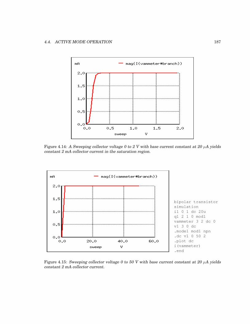
4.4. ACTIVE MODE OPERATION 187
Figure 4.14: A Sweeping collector voltage 0 to 2 V with base current constant at 20 µA yieldsconstant 2 mA collector current in the saturation region.
bipolar transistorsimulationi1 0 1 dc 20uq1 2 1 0 mod1vammeter 3 2 dc 0v1 3 0 dc.model mod1 npn.dc v1 0 50 2.plot dci(vammeter).end
Figure 4.15: Sweeping collector voltage 0 to 50 V with base current constant at 20 µA yieldsconstant 2 mA collector current.
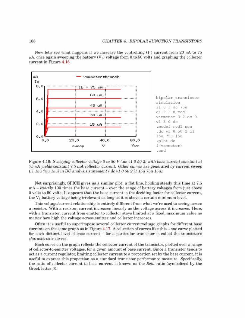
188 CHAPTER 4. BIPOLAR JUNCTION TRANSISTORS
Now let’s see what happens if we increase the controlling (I1) current from 20 µA to 75µA, once again sweeping the battery (V1) voltage from 0 to 50 volts and graphing the collectorcurrent in Figure 4.16.
bipolar transistorsimulationi1 0 1 dc 75uq1 2 1 0 mod1vammeter 3 2 dc 0v1 3 0 dc.model mod1 npn.dc v1 0 50 2 i115u 75u 15u.plot dci(vammeter).end
Figure 4.16: Sweeping collector voltage 0 to 50 V (.dc v1 0 50 2) with base current constant at75 µA yields constant 7.5 mA collector current. Other curves are generated by current sweep(i1 15u 75u 15u) in DC analysis statement (.dc v1 0 50 2 i1 15u 75u 15u).
Not surprisingly, SPICE gives us a similar plot: a flat line, holding steady this time at 7.5mA – exactly 100 times the base current – over the range of battery voltages from just above0 volts to 50 volts. It appears that the base current is the deciding factor for collector current,the V1 battery voltage being irrelevant as long as it is above a certain minimum level.
This voltage/current relationship is entirely different from what we’re used to seeing acrossa resistor. With a resistor, current increases linearly as the voltage across it increases. Here,with a transistor, current from emitter to collector stays limited at a fixed, maximum value nomatter how high the voltage across emitter and collector increases.
Often it is useful to superimpose several collector current/voltage graphs for different basecurrents on the same graph as in Figure 4.17. A collection of curves like this – one curve plottedfor each distinct level of base current – for a particular transistor is called the transistor’scharacteristic curves:
Each curve on the graph reflects the collector current of the transistor, plotted over a rangeof collector-to-emitter voltages, for a given amount of base current. Since a transistor tends toact as a current regulator, limiting collector current to a proportion set by the base current, it isuseful to express this proportion as a standard transistor performance measure. Specifically,the ratio of collector current to base current is known as the Beta ratio (symbolized by theGreek letter β):
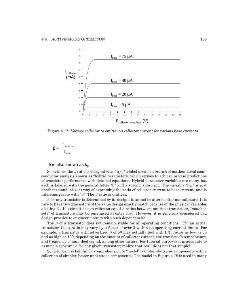
4.4. ACTIVE MODE OPERATION 189
Icollector
Ecollector-to-emitter
Ibase = 75 µA
Ibase = 40 µA
Ibase = 20 µA
Ibase = 5 µA
(mA)
0 1 2 3 4 9 105 6 7 8 11 12 13 14
0
1
2
3
4
5
6
7
8
9
(V)
Figure 4.17: Voltage collector to emitter vs collector current for various base currents.
β = Icollector
Ibase
β is also known as hfe
Sometimes the β ratio is designated as “hfe,” a label used in a branch of mathematical semi-conductor analysis known as “hybrid parameters” which strives to achieve precise predictionsof transistor performance with detailed equations. Hybrid parameter variables are many, buteach is labeled with the general letter “h” and a specific subscript. The variable “hfe” is justanother (standardized) way of expressing the ratio of collector current to base current, and isinterchangeable with “β.” The β ratio is unitless.
β for any transistor is determined by its design: it cannot be altered after manufacture. It israre to have two transistors of the same design exactly match because of the physical variablesafecting β . If a circuit design relies on equal β ratios between multiple transistors, “matchedsets” of transistors may be purchased at extra cost. However, it is generally considered baddesign practice to engineer circuits with such dependencies.
The β of a transistor does not remain stable for all operating conditions. For an actualtransistor, the β ratio may vary by a factor of over 3 within its operating current limits. Forexample, a transistor with advertised β of 50 may actually test with Ic/Ib ratios as low as 30and as high as 100, depending on the amount of collector current, the transistor’s temperature,and frequency of amplified signal, among other factors. For tutorial purposes it is adequate toassume a constant β for any given transistor; realize that real life is not that simple!
Sometimes it is helpful for comprehension to “model” complex electronic components with acollection of simpler, better-understood components. The model in Figure 4.18 is used in many
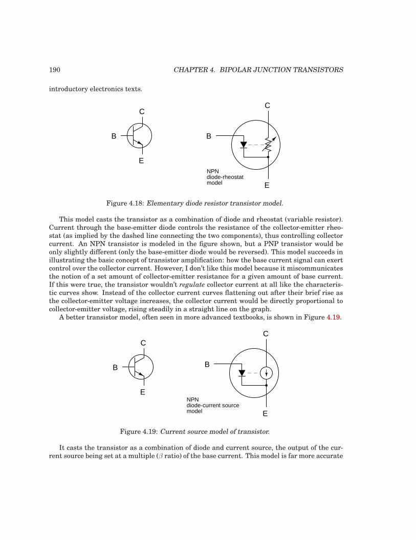
190 CHAPTER 4. BIPOLAR JUNCTION TRANSISTORS
introductory electronics texts.
NPN diode-rheostat model
B
C
E
C
E
B
Figure 4.18: Elementary diode resistor transistor model.
This model casts the transistor as a combination of diode and rheostat (variable resistor).Current through the base-emitter diode controls the resistance of the collector-emitter rheo-stat (as implied by the dashed line connecting the two components), thus controlling collectorcurrent. An NPN transistor is modeled in the figure shown, but a PNP transistor would beonly slightly different (only the base-emitter diode would be reversed). This model succeeds inillustrating the basic concept of transistor amplification: how the base current signal can exertcontrol over the collector current. However, I don’t like this model because it miscommunicatesthe notion of a set amount of collector-emitter resistance for a given amount of base current.If this were true, the transistor wouldn’t regulate collector current at all like the characteris-tic curves show. Instead of the collector current curves flattening out after their brief rise asthe collector-emitter voltage increases, the collector current would be directly proportional tocollector-emitter voltage, rising steadily in a straight line on the graph.
A better transistor model, often seen in more advanced textbooks, is shown in Figure 4.19.
B
C
E
C
E
B
NPN diode-current source model
Figure 4.19: Current source model of transistor.
It casts the transistor as a combination of diode and current source, the output of the cur-rent source being set at a multiple (β ratio) of the base current. This model is far more accurate
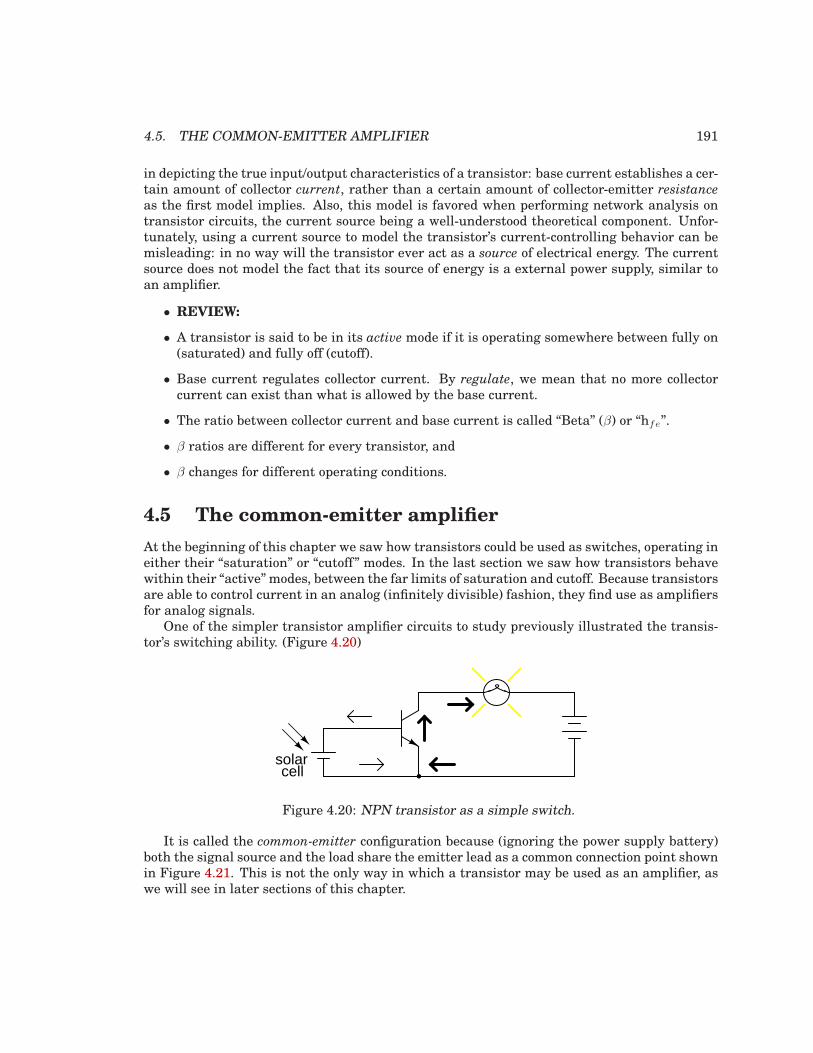
4.5. THE COMMON-EMITTER AMPLIFIER 191
in depicting the true input/output characteristics of a transistor: base current establishes a cer-tain amount of collector current, rather than a certain amount of collector-emitter resistance
as the first model implies. Also, this model is favored when performing network analysis ontransistor circuits, the current source being a well-understood theoretical component. Unfor-tunately, using a current source to model the transistor’s current-controlling behavior can bemisleading: in no way will the transistor ever act as a source of electrical energy. The currentsource does not model the fact that its source of energy is a external power supply, similar toan amplifier.
• REVIEW:
• A transistor is said to be in its active mode if it is operating somewhere between fully on(saturated) and fully off (cutoff).
• Base current regulates collector current. By regulate, we mean that no more collectorcurrent can exist than what is allowed by the base current.
• The ratio between collector current and base current is called “Beta” (β) or “hfe”.
• β ratios are different for every transistor, and
• β changes for different operating conditions.
4.5 The common-emitter amplifier
At the beginning of this chapter we saw how transistors could be used as switches, operating ineither their “saturation” or “cutoff” modes. In the last section we saw how transistors behavewithin their “active” modes, between the far limits of saturation and cutoff. Because transistorsare able to control current in an analog (infinitely divisible) fashion, they find use as amplifiersfor analog signals.
One of the simpler transistor amplifier circuits to study previously illustrated the transis-tor’s switching ability. (Figure 4.20)
solarcell
Figure 4.20: NPN transistor as a simple switch.
It is called the common-emitter configuration because (ignoring the power supply battery)both the signal source and the load share the emitter lead as a common connection point shownin Figure 4.21. This is not the only way in which a transistor may be used as an amplifier, aswe will see in later sections of this chapter.
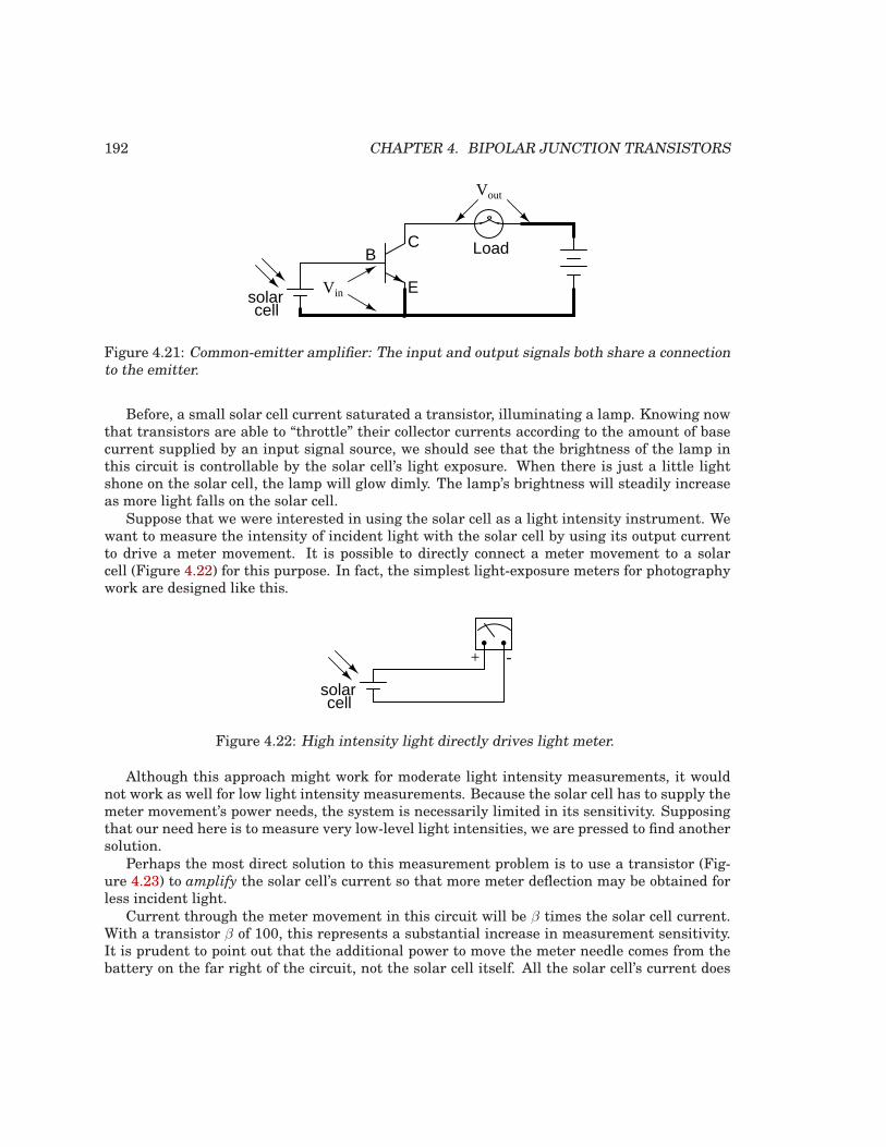
192 CHAPTER 4. BIPOLAR JUNCTION TRANSISTORS
solarcell
Vin
Vout
B
E
C Load
Figure 4.21: Common-emitter amplifier: The input and output signals both share a connectionto the emitter.
Before, a small solar cell current saturated a transistor, illuminating a lamp. Knowing nowthat transistors are able to “throttle” their collector currents according to the amount of basecurrent supplied by an input signal source, we should see that the brightness of the lamp inthis circuit is controllable by the solar cell’s light exposure. When there is just a little lightshone on the solar cell, the lamp will glow dimly. The lamp’s brightness will steadily increaseas more light falls on the solar cell.
Suppose that we were interested in using the solar cell as a light intensity instrument. Wewant to measure the intensity of incident light with the solar cell by using its output currentto drive a meter movement. It is possible to directly connect a meter movement to a solarcell (Figure 4.22) for this purpose. In fact, the simplest light-exposure meters for photographywork are designed like this.
solarcell
+ -
Figure 4.22: High intensity light directly drives light meter.
Although this approach might work for moderate light intensity measurements, it wouldnot work as well for low light intensity measurements. Because the solar cell has to supply themeter movement’s power needs, the system is necessarily limited in its sensitivity. Supposingthat our need here is to measure very low-level light intensities, we are pressed to find anothersolution.
Perhaps the most direct solution to this measurement problem is to use a transistor (Fig-ure 4.23) to amplify the solar cell’s current so that more meter deflection may be obtained forless incident light.
Current through the meter movement in this circuit will be β times the solar cell current.With a transistor β of 100, this represents a substantial increase in measurement sensitivity.It is prudent to point out that the additional power to move the meter needle comes from thebattery on the far right of the circuit, not the solar cell itself. All the solar cell’s current does
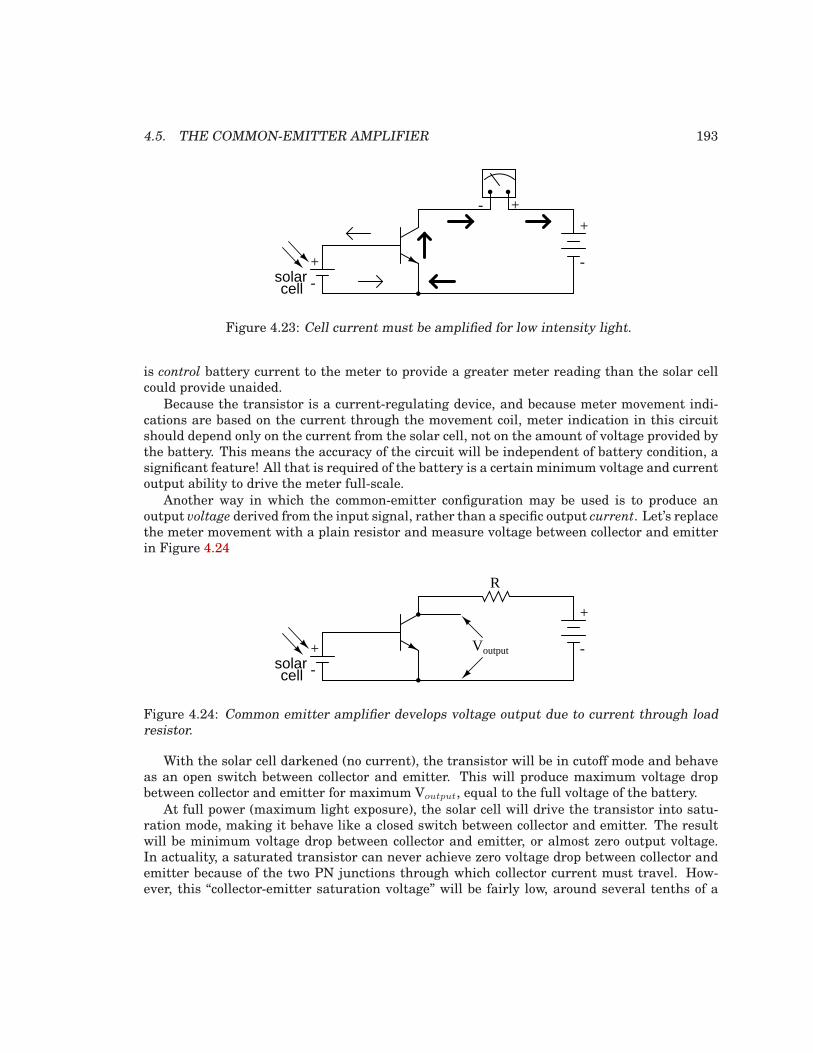
4.5. THE COMMON-EMITTER AMPLIFIER 193
solarcell
+-
+
-+
-
Figure 4.23: Cell current must be amplified for low intensity light.
is control battery current to the meter to provide a greater meter reading than the solar cellcould provide unaided.
Because the transistor is a current-regulating device, and because meter movement indi-cations are based on the current through the movement coil, meter indication in this circuitshould depend only on the current from the solar cell, not on the amount of voltage provided bythe battery. This means the accuracy of the circuit will be independent of battery condition, asignificant feature! All that is required of the battery is a certain minimum voltage and currentoutput ability to drive the meter full-scale.
Another way in which the common-emitter configuration may be used is to produce anoutput voltage derived from the input signal, rather than a specific output current. Let’s replacethe meter movement with a plain resistor and measure voltage between collector and emitterin Figure 4.24
solarcell
+
-+
-
R
Voutput
Figure 4.24: Common emitter amplifier develops voltage output due to current through loadresistor.
With the solar cell darkened (no current), the transistor will be in cutoff mode and behaveas an open switch between collector and emitter. This will produce maximum voltage dropbetween collector and emitter for maximum Voutput, equal to the full voltage of the battery.
At full power (maximum light exposure), the solar cell will drive the transistor into satu-ration mode, making it behave like a closed switch between collector and emitter. The resultwill be minimum voltage drop between collector and emitter, or almost zero output voltage.In actuality, a saturated transistor can never achieve zero voltage drop between collector andemitter because of the two PN junctions through which collector current must travel. How-ever, this “collector-emitter saturation voltage” will be fairly low, around several tenths of a
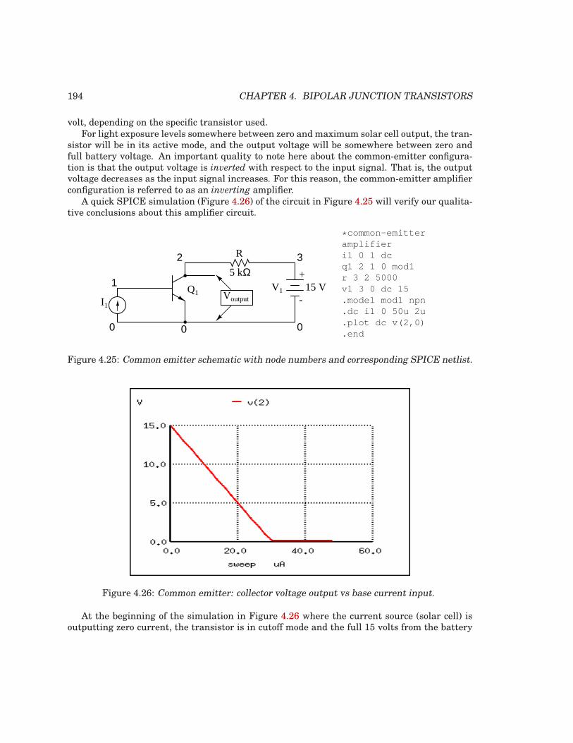
194 CHAPTER 4. BIPOLAR JUNCTION TRANSISTORS
volt, depending on the specific transistor used.For light exposure levels somewhere between zero and maximum solar cell output, the tran-
sistor will be in its active mode, and the output voltage will be somewhere between zero andfull battery voltage. An important quality to note here about the common-emitter configura-tion is that the output voltage is inverted with respect to the input signal. That is, the outputvoltage decreases as the input signal increases. For this reason, the common-emitter amplifierconfiguration is referred to as an inverting amplifier.
A quick SPICE simulation (Figure 4.26) of the circuit in Figure 4.25 will verify our qualita-tive conclusions about this amplifier circuit.
+
-
R
VoutputI1
1
0
2
0 0
35 kΩ
V1 15 VQ1
* common-emitteramplifieri1 0 1 dcq1 2 1 0 mod1r 3 2 5000v1 3 0 dc 15.model mod1 npn.dc i1 0 50u 2u.plot dc v(2,0).end
Figure 4.25: Common emitter schematic with node numbers and corresponding SPICE netlist.
Figure 4.26: Common emitter: collector voltage output vs base current input.
At the beginning of the simulation in Figure 4.26 where the current source (solar cell) isoutputting zero current, the transistor is in cutoff mode and the full 15 volts from the battery
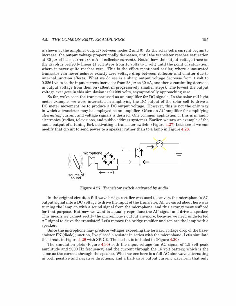
4.5. THE COMMON-EMITTER AMPLIFIER 195
is shown at the amplifier output (between nodes 2 and 0). As the solar cell’s current begins toincrease, the output voltage proportionally decreases, until the transistor reaches saturationat 30 µA of base current (3 mA of collector current). Notice how the output voltage trace onthe graph is perfectly linear (1 volt steps from 15 volts to 1 volt) until the point of saturation,where it never quite reaches zero. This is the effect mentioned earlier, where a saturatedtransistor can never achieve exactly zero voltage drop between collector and emitter due tointernal junction effects. What we do see is a sharp output voltage decrease from 1 volt to0.2261 volts as the input current increases from 28 µA to 30 µA, and then a continuing decreasein output voltage from then on (albeit in progressively smaller steps). The lowest the outputvoltage ever gets in this simulation is 0.1299 volts, asymptotically approaching zero.
So far, we’ve seen the transistor used as an amplifier for DC signals. In the solar cell lightmeter example, we were interested in amplifying the DC output of the solar cell to drive aDC meter movement, or to produce a DC output voltage. However, this is not the only wayin which a transistor may be employed as an amplifier. Often an AC amplifier for amplifyingalternating current and voltage signals is desired. One common application of this is in audioelectronics (radios, televisions, and public-address systems). Earlier, we saw an example of theaudio output of a tuning fork activating a transistor switch. (Figure 4.27) Let’s see if we canmodify that circuit to send power to a speaker rather than to a lamp in Figure 4.28.
microphone
source ofsound
Figure 4.27: Transistor switch activated by audio.
In the original circuit, a full-wave bridge rectifier was used to convert the microphone’s ACoutput signal into a DC voltage to drive the input of the transistor. All we cared about here wasturning the lamp on with a sound signal from the microphone, and this arrangement sufficedfor that purpose. But now we want to actually reproduce the AC signal and drive a speaker.This means we cannot rectify the microphone’s output anymore, because we need undistortedAC signal to drive the transistor! Let’s remove the bridge rectifier and replace the lamp with aspeaker:
Since the microphone may produce voltages exceeding the forward voltage drop of the base-emitter PN (diode) junction, I’ve placed a resistor in series with the microphone. Let’s simulatethe circuit in Figure 4.29 with SPICE. The netlist is included in (Figure 4.30)
The simulation plots (Figure 4.30) both the input voltage (an AC signal of 1.5 volt peakamplitude and 2000 Hz frequency) and the current through the 15 volt battery, which is thesame as the current through the speaker. What we see here is a full AC sine wave alternatingin both positive and negative directions, and a half-wave output current waveform that only
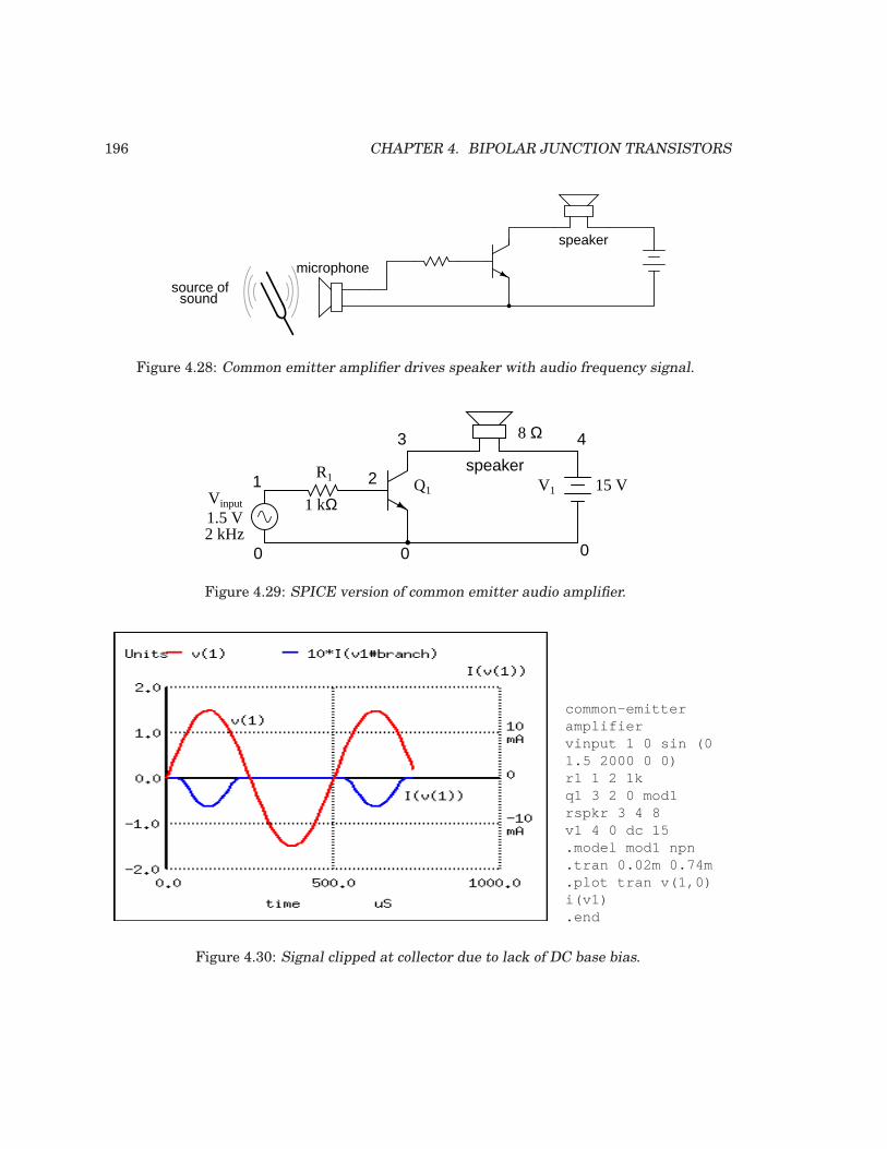
196 CHAPTER 4. BIPOLAR JUNCTION TRANSISTORS
microphonesource of
sound
speaker
Figure 4.28: Common emitter amplifier drives speaker with audio frequency signal.
speakerV1 15 VQ1
R1
1 kΩ
8 Ω
1
0 0 0
2
3 4
Vinput
1.5 V2 kHz
Figure 4.29: SPICE version of common emitter audio amplifier.
common-emitteramplifiervinput 1 0 sin (01.5 2000 0 0)r1 1 2 1kq1 3 2 0 mod1rspkr 3 4 8v1 4 0 dc 15.model mod1 npn.tran 0.02m 0.74m.plot tran v(1,0)i(v1).end
Figure 4.30: Signal clipped at collector due to lack of DC base bias.
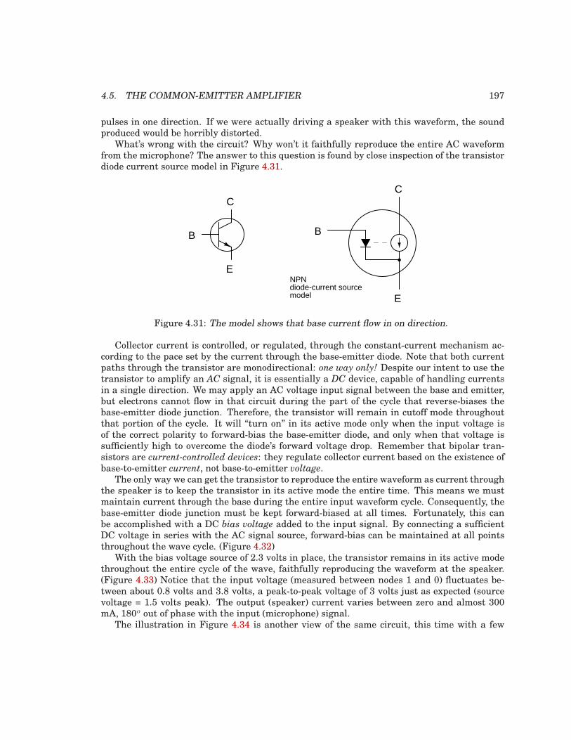
4.5. THE COMMON-EMITTER AMPLIFIER 197
pulses in one direction. If we were actually driving a speaker with this waveform, the soundproduced would be horribly distorted.
What’s wrong with the circuit? Why won’t it faithfully reproduce the entire AC waveformfrom the microphone? The answer to this question is found by close inspection of the transistordiode current source model in Figure 4.31.
B
C
E
C
E
B
NPN diode-current source model
Figure 4.31: The model shows that base current flow in on direction.
Collector current is controlled, or regulated, through the constant-current mechanism ac-cording to the pace set by the current through the base-emitter diode. Note that both currentpaths through the transistor are monodirectional: one way only! Despite our intent to use thetransistor to amplify an AC signal, it is essentially a DC device, capable of handling currentsin a single direction. We may apply an AC voltage input signal between the base and emitter,but electrons cannot flow in that circuit during the part of the cycle that reverse-biases thebase-emitter diode junction. Therefore, the transistor will remain in cutoff mode throughoutthat portion of the cycle. It will “turn on” in its active mode only when the input voltage isof the correct polarity to forward-bias the base-emitter diode, and only when that voltage issufficiently high to overcome the diode’s forward voltage drop. Remember that bipolar tran-sistors are current-controlled devices: they regulate collector current based on the existence ofbase-to-emitter current, not base-to-emitter voltage.
The only way we can get the transistor to reproduce the entire waveform as current throughthe speaker is to keep the transistor in its active mode the entire time. This means we mustmaintain current through the base during the entire input waveform cycle. Consequently, thebase-emitter diode junction must be kept forward-biased at all times. Fortunately, this canbe accomplished with a DC bias voltage added to the input signal. By connecting a sufficientDC voltage in series with the AC signal source, forward-bias can be maintained at all pointsthroughout the wave cycle. (Figure 4.32)
With the bias voltage source of 2.3 volts in place, the transistor remains in its active modethroughout the entire cycle of the wave, faithfully reproducing the waveform at the speaker.(Figure 4.33) Notice that the input voltage (measured between nodes 1 and 0) fluctuates be-tween about 0.8 volts and 3.8 volts, a peak-to-peak voltage of 3 volts just as expected (sourcevoltage = 1.5 volts peak). The output (speaker) current varies between zero and almost 300mA, 180o out of phase with the input (microphone) signal.
The illustration in Figure 4.34 is another view of the same circuit, this time with a few
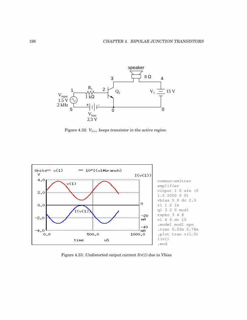
198 CHAPTER 4. BIPOLAR JUNCTION TRANSISTORS
speaker
V1 15 VQ1
R1
1 kΩ
8 Ω
1
0 0
2
3 4
Vinput
1.5 V2 kHz
Vbias
5
2.3 V
+ -
Figure 4.32: Vbias keeps transistor in the active region.
common-emitteramplifiervinput 1 5 sin (01.5 2000 0 0)vbias 5 0 dc 2.3r1 1 2 1kq1 3 2 0 mod1rspkr 3 4 8v1 4 0 dc 15.model mod1 npn.tran 0.02m 0.78m.plot tran v(1,0)i(v1).end
Figure 4.33: Undistorted output current I(v(1) due to Vbias
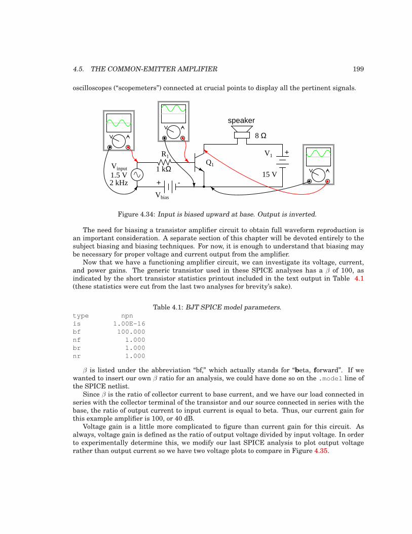
4.5. THE COMMON-EMITTER AMPLIFIER 199
oscilloscopes (“scopemeters”) connected at crucial points to display all the pertinent signals.
speaker
V1
15 V
Q1
R1
1 kΩ
8 Ω
Vinput
1.5 V2 kHz
Vbias
+ -
+
Figure 4.34: Input is biased upward at base. Output is inverted.
The need for biasing a transistor amplifier circuit to obtain full waveform reproduction isan important consideration. A separate section of this chapter will be devoted entirely to thesubject biasing and biasing techniques. For now, it is enough to understand that biasing maybe necessary for proper voltage and current output from the amplifier.
Now that we have a functioning amplifier circuit, we can investigate its voltage, current,and power gains. The generic transistor used in these SPICE analyses has a β of 100, asindicated by the short transistor statistics printout included in the text output in Table 4.1(these statistics were cut from the last two analyses for brevity’s sake).
Table 4.1: BJT SPICE model parameters.type npnis 1.00E-16bf 100.000nf 1.000br 1.000nr 1.000
β is listed under the abbreviation “bf,” which actually stands for “beta, forward”. If wewanted to insert our own β ratio for an analysis, we could have done so on the .model line ofthe SPICE netlist.
Since β is the ratio of collector current to base current, and we have our load connected inseries with the collector terminal of the transistor and our source connected in series with thebase, the ratio of output current to input current is equal to beta. Thus, our current gain forthis example amplifier is 100, or 40 dB.
Voltage gain is a little more complicated to figure than current gain for this circuit. Asalways, voltage gain is defined as the ratio of output voltage divided by input voltage. In orderto experimentally determine this, we modify our last SPICE analysis to plot output voltagerather than output current so we have two voltage plots to compare in Figure 4.35.
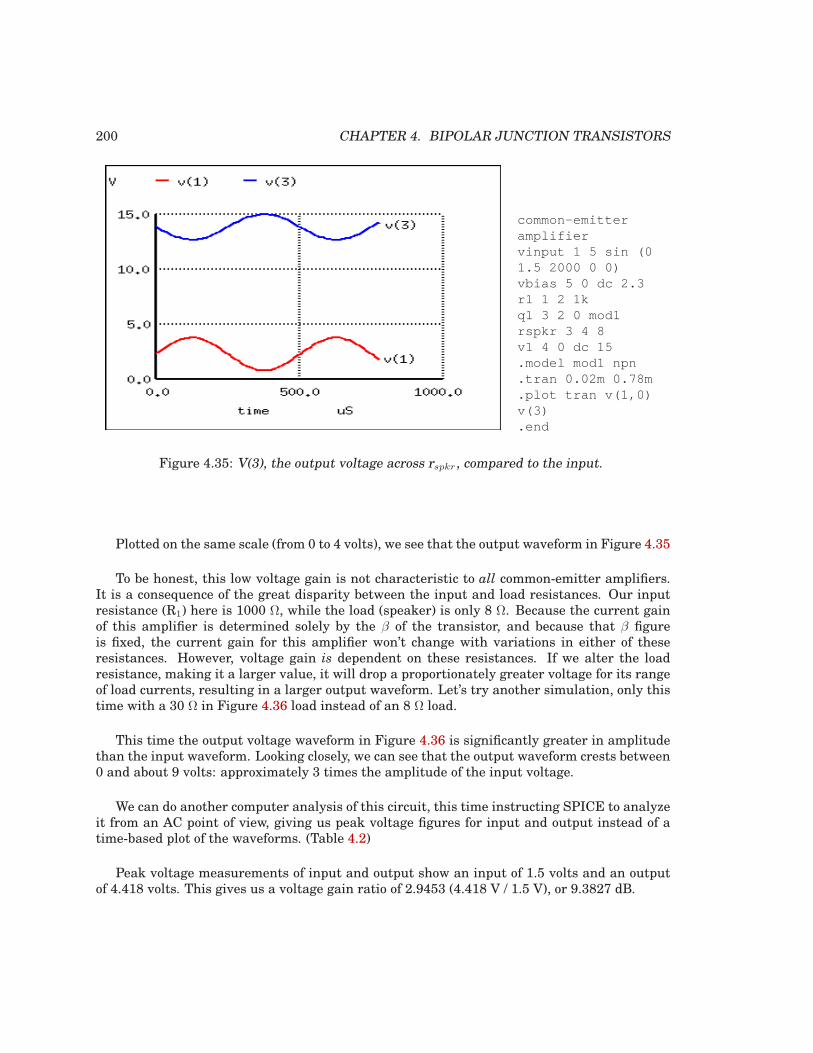
200 CHAPTER 4. BIPOLAR JUNCTION TRANSISTORS
common-emitteramplifiervinput 1 5 sin (01.5 2000 0 0)vbias 5 0 dc 2.3r1 1 2 1kq1 3 2 0 mod1rspkr 3 4 8v1 4 0 dc 15.model mod1 npn.tran 0.02m 0.78m.plot tran v(1,0)v(3).end
Figure 4.35: V(3), the output voltage across rspkr, compared to the input.
Plotted on the same scale (from 0 to 4 volts), we see that the output waveform in Figure 4.35
To be honest, this low voltage gain is not characteristic to all common-emitter amplifiers.It is a consequence of the great disparity between the input and load resistances. Our inputresistance (R1) here is 1000 Ω, while the load (speaker) is only 8 Ω. Because the current gainof this amplifier is determined solely by the β of the transistor, and because that β figureis fixed, the current gain for this amplifier won’t change with variations in either of theseresistances. However, voltage gain is dependent on these resistances. If we alter the loadresistance, making it a larger value, it will drop a proportionately greater voltage for its rangeof load currents, resulting in a larger output waveform. Let’s try another simulation, only thistime with a 30 Ω in Figure 4.36 load instead of an 8 Ω load.
This time the output voltage waveform in Figure 4.36 is significantly greater in amplitudethan the input waveform. Looking closely, we can see that the output waveform crests between0 and about 9 volts: approximately 3 times the amplitude of the input voltage.
We can do another computer analysis of this circuit, this time instructing SPICE to analyzeit from an AC point of view, giving us peak voltage figures for input and output instead of atime-based plot of the waveforms. (Table 4.2)
Peak voltage measurements of input and output show an input of 1.5 volts and an outputof 4.418 volts. This gives us a voltage gain ratio of 2.9453 (4.418 V / 1.5 V), or 9.3827 dB.
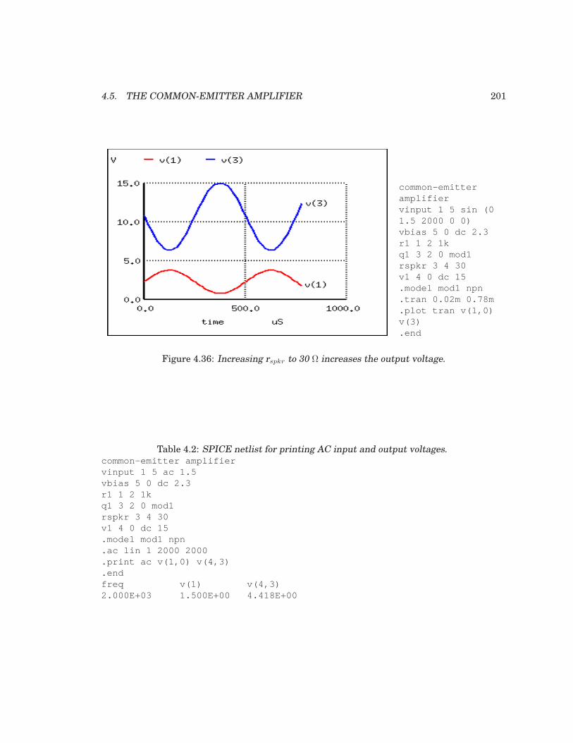
4.5. THE COMMON-EMITTER AMPLIFIER 201
common-emitteramplifiervinput 1 5 sin (01.5 2000 0 0)vbias 5 0 dc 2.3r1 1 2 1kq1 3 2 0 mod1rspkr 3 4 30v1 4 0 dc 15.model mod1 npn.tran 0.02m 0.78m.plot tran v(1,0)v(3).end
Figure 4.36: Increasing rspkr to 30 Ω increases the output voltage.
Table 4.2: SPICE netlist for printing AC input and output voltages.common-emitter amplifiervinput 1 5 ac 1.5vbias 5 0 dc 2.3r1 1 2 1kq1 3 2 0 mod1rspkr 3 4 30v1 4 0 dc 15.model mod1 npn.ac lin 1 2000 2000.print ac v(1,0) v(4,3).endfreq v(1) v(4,3)2.000E+03 1.500E+00 4.418E+00
202 CHAPTER 4. BIPOLAR JUNCTION TRANSISTORS
AV = Vout
Vin
AV = 4.418 V1.5 V
AV = 2.9453
AV(dB) = 20 log AV(ratio)
AV(dB) = 9.3827 dB
AV(dB) = 20 log 2.9453
Because the current gain of the common-emitter amplifier is fixed by β, and since the in-put and output voltages will be equal to the input and output currents multiplied by theirrespective resistors, we can derive an equation for approximate voltage gain:
AV = β Rout
Rin
AV = (100) 30 Ω1000 Ω
AV = 3
AV(dB) = 20 log AV(ratio)
AV(dB) = 20 log 3
AV(dB) = 9.5424 dB
As you can see, the predicted results for voltage gain are quite close to the simulated results.With perfectly linear transistor behavior, the two sets of figures would exactly match. SPICEdoes a reasonable job of accounting for the many “quirks” of bipolar transistor function in itsanalysis, hence the slight mismatch in voltage gain based on SPICE’s output.
These voltage gains remain the same regardless of where we measure output voltage inthe circuit: across collector and emitter, or across the series load resistor as we did in thelast analysis. The amount of output voltage change for any given amount of input voltagewill remain the same. Consider the two following SPICE analyses as proof of this. The firstsimulation in Figure 4.37 is time-based, to provide a plot of input and output voltages. Youwill notice that the two signals are 180o out of phase with each other. The second simulationin Table 4.3 is an AC analysis, to provide simple, peak voltage readings for input and output.
We still have a peak output voltage of 4.418 volts with a peak input voltage of 1.5 volts. Theonly difference from the last set of simulations is the phase of the output voltage.
So far, the example circuits shown in this section have all used NPN transistors. PNP tran-
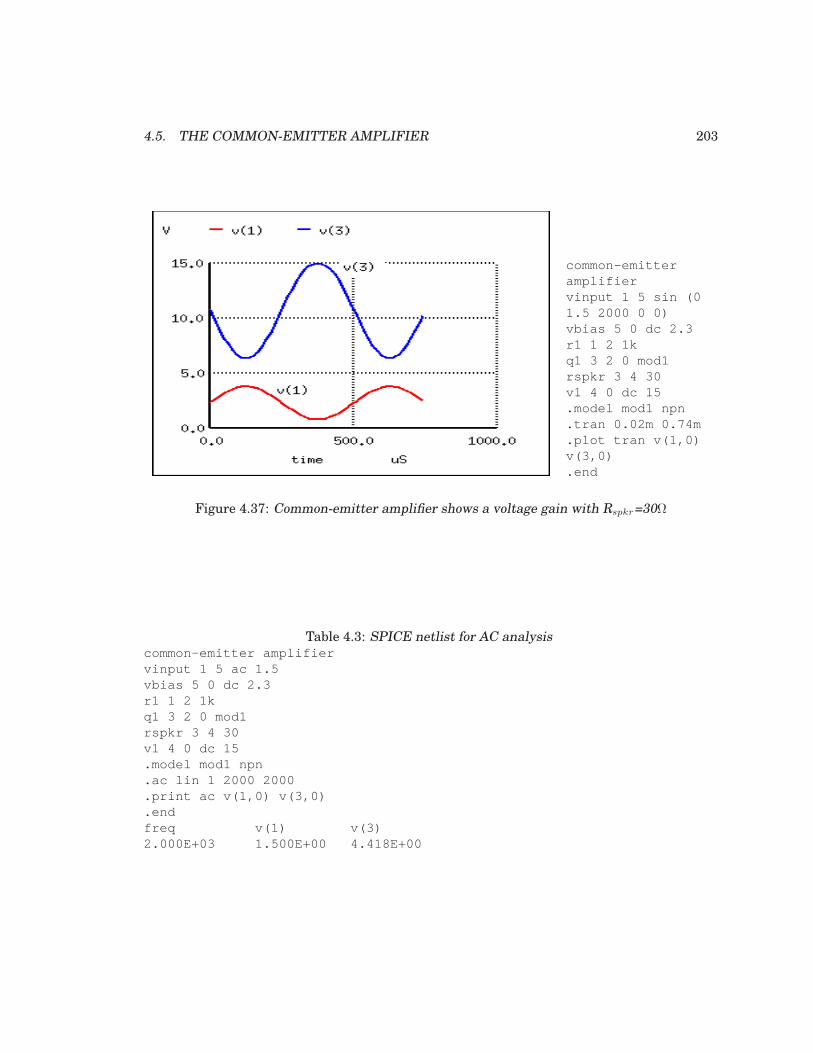
4.5. THE COMMON-EMITTER AMPLIFIER 203
common-emitteramplifiervinput 1 5 sin (01.5 2000 0 0)vbias 5 0 dc 2.3r1 1 2 1kq1 3 2 0 mod1rspkr 3 4 30v1 4 0 dc 15.model mod1 npn.tran 0.02m 0.74m.plot tran v(1,0)v(3,0).end
Figure 4.37: Common-emitter amplifier shows a voltage gain with Rspkr=30Ω
Table 4.3: SPICE netlist for AC analysiscommon-emitter amplifiervinput 1 5 ac 1.5vbias 5 0 dc 2.3r1 1 2 1kq1 3 2 0 mod1rspkr 3 4 30v1 4 0 dc 15.model mod1 npn.ac lin 1 2000 2000.print ac v(1,0) v(3,0).endfreq v(1) v(3)2.000E+03 1.500E+00 4.418E+00
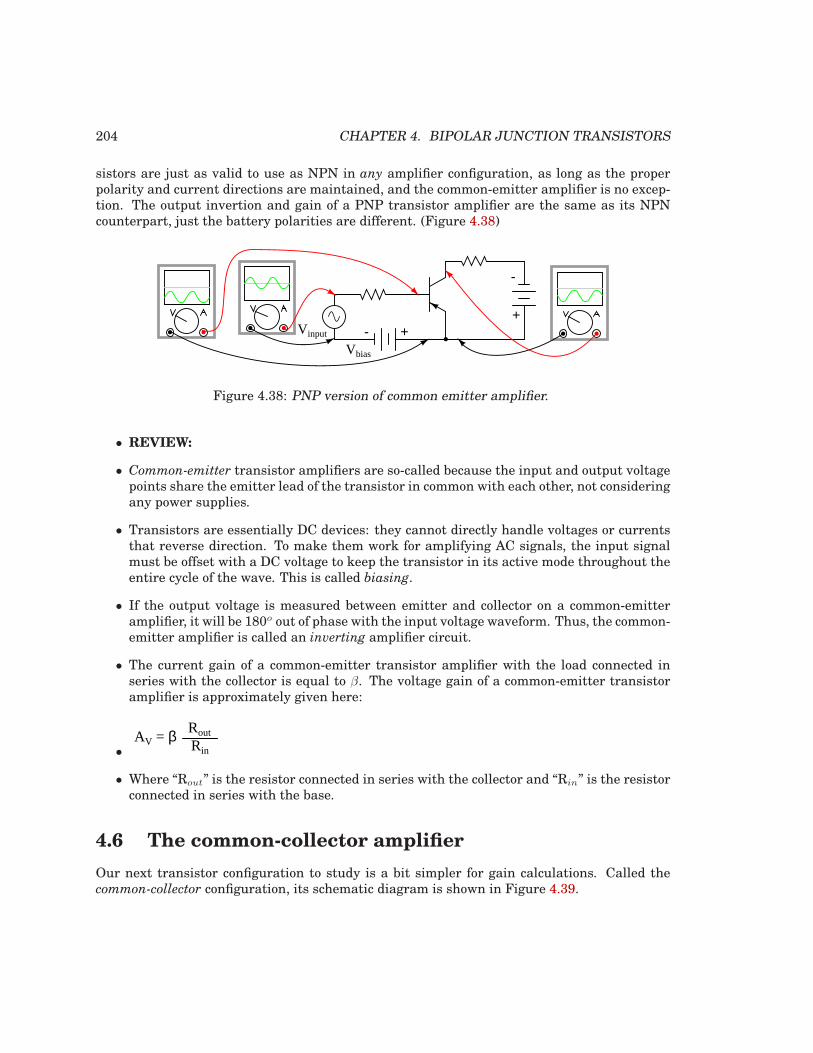
204 CHAPTER 4. BIPOLAR JUNCTION TRANSISTORS
sistors are just as valid to use as NPN in any amplifier configuration, as long as the properpolarity and current directions are maintained, and the common-emitter amplifier is no excep-tion. The output invertion and gain of a PNP transistor amplifier are the same as its NPNcounterpart, just the battery polarities are different. (Figure 4.38)
Vinput
Vbias
+-
-
+
Figure 4.38: PNP version of common emitter amplifier.
• REVIEW:
• Common-emitter transistor amplifiers are so-called because the input and output voltagepoints share the emitter lead of the transistor in common with each other, not consideringany power supplies.
• Transistors are essentially DC devices: they cannot directly handle voltages or currentsthat reverse direction. To make them work for amplifying AC signals, the input signalmust be offset with a DC voltage to keep the transistor in its active mode throughout theentire cycle of the wave. This is called biasing.
• If the output voltage is measured between emitter and collector on a common-emitteramplifier, it will be 180o out of phase with the input voltage waveform. Thus, the common-emitter amplifier is called an inverting amplifier circuit.
• The current gain of a common-emitter transistor amplifier with the load connected inseries with the collector is equal to β. The voltage gain of a common-emitter transistoramplifier is approximately given here:
•AV = β Rout
Rin
• Where “Rout” is the resistor connected in series with the collector and “Rin” is the resistorconnected in series with the base.
4.6 The common-collector amplifier
Our next transistor configuration to study is a bit simpler for gain calculations. Called thecommon-collector configuration, its schematic diagram is shown in Figure 4.39.
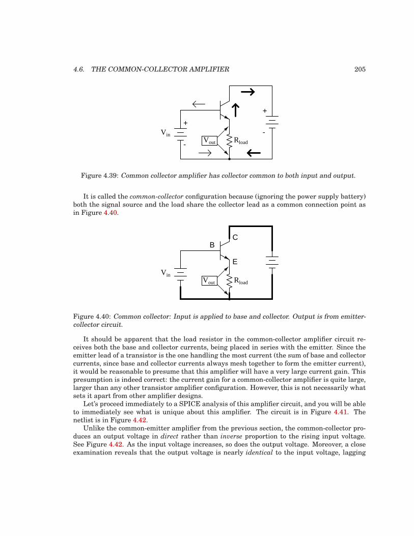
4.6. THE COMMON-COLLECTOR AMPLIFIER 205
Rload
VinVout
+
-+
-
Figure 4.39: Common collector amplifier has collector common to both input and output.
It is called the common-collector configuration because (ignoring the power supply battery)both the signal source and the load share the collector lead as a common connection point asin Figure 4.40.
Rload
VinVout
BC
E
Figure 4.40: Common collector: Input is applied to base and collector. Output is from emitter-collector circuit.
It should be apparent that the load resistor in the common-collector amplifier circuit re-ceives both the base and collector currents, being placed in series with the emitter. Since theemitter lead of a transistor is the one handling the most current (the sum of base and collectorcurrents, since base and collector currents always mesh together to form the emitter current),it would be reasonable to presume that this amplifier will have a very large current gain. Thispresumption is indeed correct: the current gain for a common-collector amplifier is quite large,larger than any other transistor amplifier configuration. However, this is not necessarily whatsets it apart from other amplifier designs.
Let’s proceed immediately to a SPICE analysis of this amplifier circuit, and you will be ableto immediately see what is unique about this amplifier. The circuit is in Figure 4.41. Thenetlist is in Figure 4.42.
Unlike the common-emitter amplifier from the previous section, the common-collector pro-duces an output voltage in direct rather than inverse proportion to the rising input voltage.See Figure 4.42. As the input voltage increases, so does the output voltage. Moreover, a closeexamination reveals that the output voltage is nearly identical to the input voltage, lagging
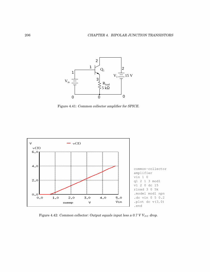
206 CHAPTER 4. BIPOLAR JUNCTION TRANSISTORS
RloadVin
V1 15 V
Q1
5 kΩ
1
0 0 0
1
2
3
2
Figure 4.41: Common collector amplifier for SPICE.
common-collectoramplifiervin 1 0q1 2 1 3 mod1v1 2 0 dc 15rload 3 0 5k.model mod1 npn.dc vin 0 5 0.2.plot dc v(3,0).end
Figure 4.42: Common collector: Output equals input less a 0.7 V VBE drop.
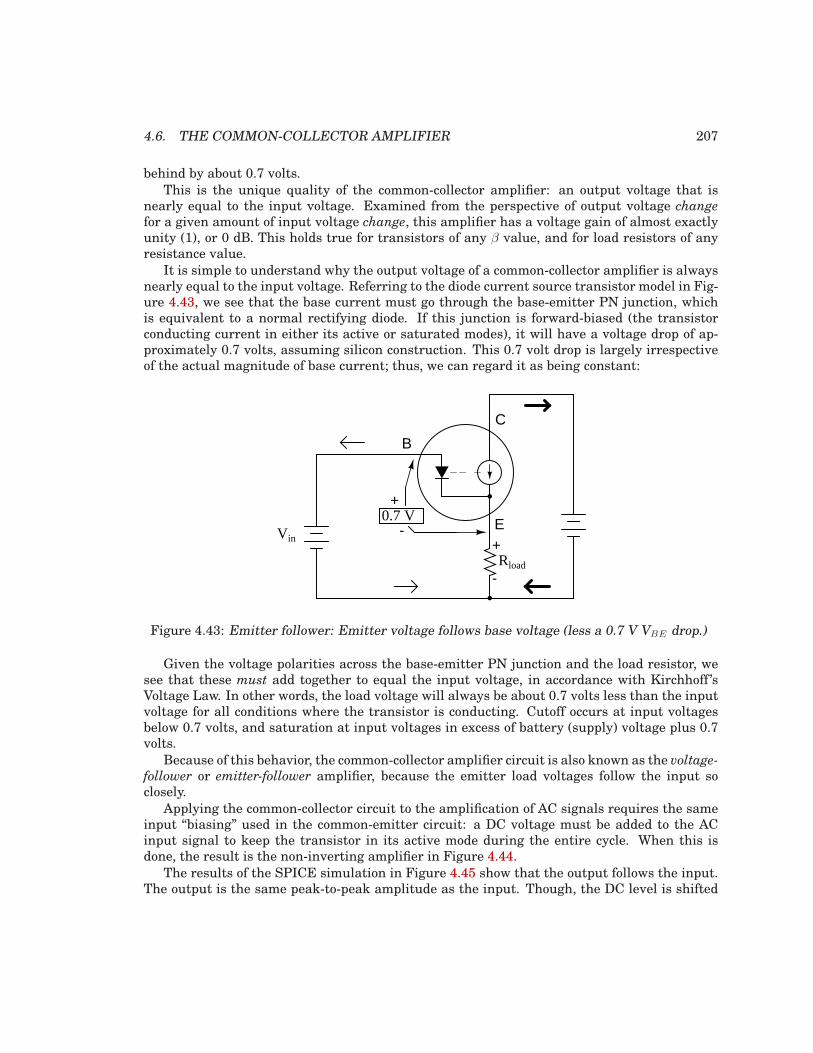
4.6. THE COMMON-COLLECTOR AMPLIFIER 207
behind by about 0.7 volts.
This is the unique quality of the common-collector amplifier: an output voltage that isnearly equal to the input voltage. Examined from the perspective of output voltage change
for a given amount of input voltage change, this amplifier has a voltage gain of almost exactlyunity (1), or 0 dB. This holds true for transistors of any β value, and for load resistors of anyresistance value.
It is simple to understand why the output voltage of a common-collector amplifier is alwaysnearly equal to the input voltage. Referring to the diode current source transistor model in Fig-ure 4.43, we see that the base current must go through the base-emitter PN junction, whichis equivalent to a normal rectifying diode. If this junction is forward-biased (the transistorconducting current in either its active or saturated modes), it will have a voltage drop of ap-proximately 0.7 volts, assuming silicon construction. This 0.7 volt drop is largely irrespectiveof the actual magnitude of base current; thus, we can regard it as being constant:
C
E
B
Rload
Vin
0.7 V+
-+
-
Figure 4.43: Emitter follower: Emitter voltage follows base voltage (less a 0.7 V VBE drop.)
Given the voltage polarities across the base-emitter PN junction and the load resistor, wesee that these must add together to equal the input voltage, in accordance with Kirchhoff ’sVoltage Law. In other words, the load voltage will always be about 0.7 volts less than the inputvoltage for all conditions where the transistor is conducting. Cutoff occurs at input voltagesbelow 0.7 volts, and saturation at input voltages in excess of battery (supply) voltage plus 0.7volts.
Because of this behavior, the common-collector amplifier circuit is also known as the voltage-follower or emitter-follower amplifier, because the emitter load voltages follow the input soclosely.
Applying the common-collector circuit to the amplification of AC signals requires the sameinput “biasing” used in the common-emitter circuit: a DC voltage must be added to the ACinput signal to keep the transistor in its active mode during the entire cycle. When this isdone, the result is the non-inverting amplifier in Figure 4.44.
The results of the SPICE simulation in Figure 4.45 show that the output follows the input.The output is the same peak-to-peak amplitude as the input. Though, the DC level is shifted
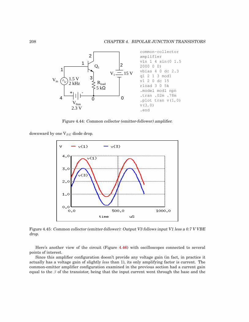
208 CHAPTER 4. BIPOLAR JUNCTION TRANSISTORS
RloadVin
V1 15 V
Q1
5 kΩ
1
0 0
1
2
3
2
1.5 V2 kHz
4Vbias
+ -
2.3 V
common-collectoramplifiervin 1 4 sin(0 1.52000 0 0)vbias 4 0 dc 2.3q1 2 1 3 mod1v1 2 0 dc 15rload 3 0 5k.model mod1 npn.tran .02m .78m.plot tran v(1,0)v(3,0).end
Figure 4.44: Common collector (emitter-follower) amplifier.
downward by one VBE diode drop.
Figure 4.45: Common collector (emitter-follower): Output V3 follows input V1 less a 0.7 V VBEdrop.
Here’s another view of the circuit (Figure 4.46) with oscilloscopes connected to severalpoints of interest.
Since this amplifier configuration doesn’t provide any voltage gain (in fact, in practice itactually has a voltage gain of slightly less than 1), its only amplifying factor is current. Thecommon-emitter amplifier configuration examined in the previous section had a current gainequal to the β of the transistor, being that the input current went through the base and the
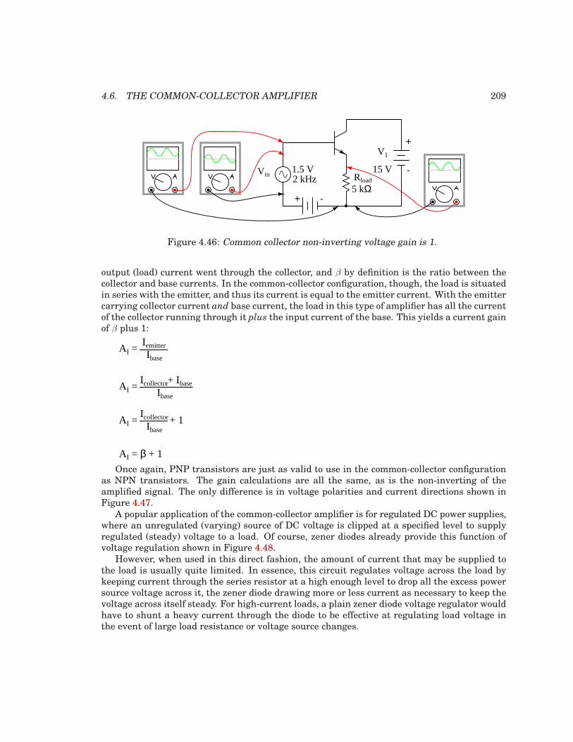
4.6. THE COMMON-COLLECTOR AMPLIFIER 209
RloadVin
V1
15 V
5 kΩ
1.5 V2 kHz
+ -
+
-
Figure 4.46: Common collector non-inverting voltage gain is 1.
output (load) current went through the collector, and β by definition is the ratio between thecollector and base currents. In the common-collector configuration, though, the load is situatedin series with the emitter, and thus its current is equal to the emitter current. With the emittercarrying collector current and base current, the load in this type of amplifier has all the currentof the collector running through it plus the input current of the base. This yields a current gainof β plus 1:
AI = Iemitter
Ibase
AI = Ibase
Icollector+ Ibase
AI = Icollector
Ibase+ 1
AI = β + 1
Once again, PNP transistors are just as valid to use in the common-collector configurationas NPN transistors. The gain calculations are all the same, as is the non-inverting of theamplified signal. The only difference is in voltage polarities and current directions shown inFigure 4.47.
A popular application of the common-collector amplifier is for regulated DC power supplies,where an unregulated (varying) source of DC voltage is clipped at a specified level to supplyregulated (steady) voltage to a load. Of course, zener diodes already provide this function ofvoltage regulation shown in Figure 4.48.
However, when used in this direct fashion, the amount of current that may be supplied tothe load is usually quite limited. In essence, this circuit regulates voltage across the load bykeeping current through the series resistor at a high enough level to drop all the excess powersource voltage across it, the zener diode drawing more or less current as necessary to keep thevoltage across itself steady. For high-current loads, a plain zener diode voltage regulator wouldhave to shunt a heavy current through the diode to be effective at regulating load voltage inthe event of large load resistance or voltage source changes.
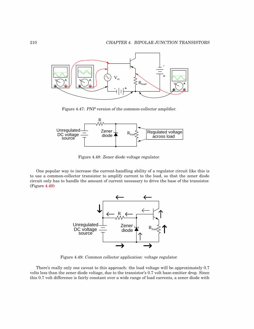
210 CHAPTER 4. BIPOLAR JUNCTION TRANSISTORS
Rload
Vin
+-
-
+
Figure 4.47: PNP version of the common-collector amplifier.
RloadUnregulatedDC voltage
source
R
Regulated voltageacross load
Zenerdiode
Figure 4.48: Zener diode voltage regulator.
One popular way to increase the current-handling ability of a regulator circuit like this isto use a common-collector transistor to amplify current to the load, so that the zener diodecircuit only has to handle the amount of current necessary to drive the base of the transistor.(Figure 4.49)
RloadUnregulatedDC voltage
source
R
Zenerdiode
Figure 4.49: Common collector application: voltage regulator.
There’s really only one caveat to this approach: the load voltage will be approximately 0.7volts less than the zener diode voltage, due to the transistor’s 0.7 volt base-emitter drop. Sincethis 0.7 volt difference is fairly constant over a wide range of load currents, a zener diode with
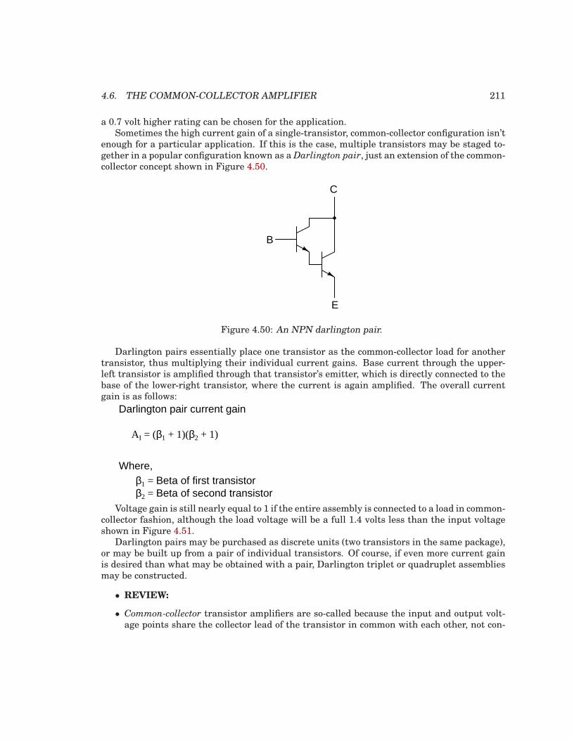
4.6. THE COMMON-COLLECTOR AMPLIFIER 211
a 0.7 volt higher rating can be chosen for the application.Sometimes the high current gain of a single-transistor, common-collector configuration isn’t
enough for a particular application. If this is the case, multiple transistors may be staged to-gether in a popular configuration known as aDarlington pair, just an extension of the common-collector concept shown in Figure 4.50.
B
C
E
Figure 4.50: An NPN darlington pair.
Darlington pairs essentially place one transistor as the common-collector load for anothertransistor, thus multiplying their individual current gains. Base current through the upper-left transistor is amplified through that transistor’s emitter, which is directly connected to thebase of the lower-right transistor, where the current is again amplified. The overall currentgain is as follows:
AI = (β1 + 1)(β2 + 1)
Darlington pair current gain
Where,β1 = Beta of first transistorβ2 = Beta of second transistor
Voltage gain is still nearly equal to 1 if the entire assembly is connected to a load in common-collector fashion, although the load voltage will be a full 1.4 volts less than the input voltageshown in Figure 4.51.
Darlington pairs may be purchased as discrete units (two transistors in the same package),or may be built up from a pair of individual transistors. Of course, if even more current gainis desired than what may be obtained with a pair, Darlington triplet or quadruplet assembliesmay be constructed.
• REVIEW:
• Common-collector transistor amplifiers are so-called because the input and output volt-age points share the collector lead of the transistor in common with each other, not con-
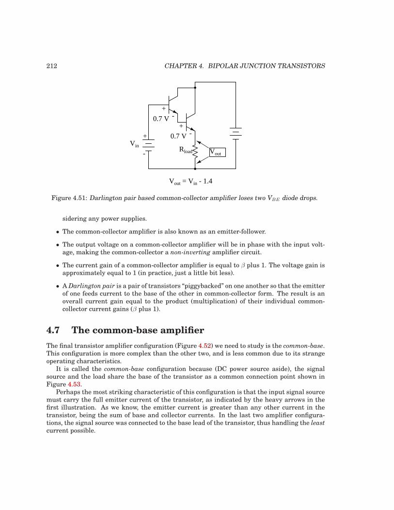
212 CHAPTER 4. BIPOLAR JUNCTION TRANSISTORS
Rload
VinVout
Vout = Vin - 1.4
+
-
+-0.7 V
+-0.7 V
Figure 4.51: Darlington pair based common-collector amplifier loses two VBE diode drops.
sidering any power supplies.
• The common-collector amplifier is also known as an emitter-follower.
• The output voltage on a common-collector amplifier will be in phase with the input volt-age, making the common-collector a non-inverting amplifier circuit.
• The current gain of a common-collector amplifier is equal to β plus 1. The voltage gain isapproximately equal to 1 (in practice, just a little bit less).
• ADarlington pair is a pair of transistors “piggybacked” on one another so that the emitterof one feeds current to the base of the other in common-collector form. The result is anoverall current gain equal to the product (multiplication) of their individual common-collector current gains (β plus 1).
4.7 The common-base amplifier
The final transistor amplifier configuration (Figure 4.52) we need to study is the common-base.This configuration is more complex than the other two, and is less common due to its strangeoperating characteristics.
It is called the common-base configuration because (DC power source aside), the signalsource and the load share the base of the transistor as a common connection point shown inFigure 4.53.
Perhaps the most striking characteristic of this configuration is that the input signal sourcemust carry the full emitter current of the transistor, as indicated by the heavy arrows in thefirst illustration. As we know, the emitter current is greater than any other current in thetransistor, being the sum of base and collector currents. In the last two amplifier configura-tions, the signal source was connected to the base lead of the transistor, thus handling the leastcurrent possible.
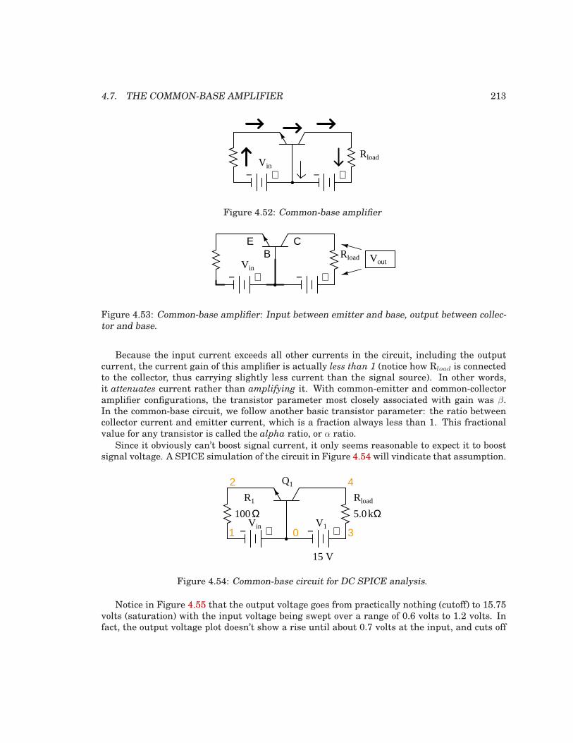
4.7. THE COMMON-BASE AMPLIFIER 213
RloadVin
+−+−
Figure 4.52: Common-base amplifier
BCE
VoutRload
Vin
+−+−
Figure 4.53: Common-base amplifier: Input between emitter and base, output between collec-tor and base.
Because the input current exceeds all other currents in the circuit, including the outputcurrent, the current gain of this amplifier is actually less than 1 (notice how Rload is connectedto the collector, thus carrying slightly less current than the signal source). In other words,it attenuates current rather than amplifying it. With common-emitter and common-collectoramplifier configurations, the transistor parameter most closely associated with gain was β.In the common-base circuit, we follow another basic transistor parameter: the ratio betweencollector current and emitter current, which is a fraction always less than 1. This fractionalvalue for any transistor is called the alpha ratio, or α ratio.
Since it obviously can’t boost signal current, it only seems reasonable to expect it to boostsignal voltage. A SPICE simulation of the circuit in Figure 4.54 will vindicate that assumption.
Rload
Vin +−+−V1
R1
Q1
15 V
0
4
31
2
5.0kΩ100Ω
Figure 4.54: Common-base circuit for DC SPICE analysis.
Notice in Figure 4.55 that the output voltage goes from practically nothing (cutoff) to 15.75volts (saturation) with the input voltage being swept over a range of 0.6 volts to 1.2 volts. Infact, the output voltage plot doesn’t show a rise until about 0.7 volts at the input, and cuts off
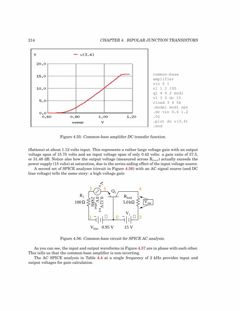
214 CHAPTER 4. BIPOLAR JUNCTION TRANSISTORS
common-baseamplifiervin 0 1r1 1 2 100q1 4 0 2 mod1v1 3 0 dc 15rload 3 4 5k.model mod1 npn.dc vin 0.6 1.2.02.plot dc v(3,4).end
Figure 4.55: Common-base amplifier DC transfer function.
(flattens) at about 1.12 volts input. This represents a rather large voltage gain with an outputvoltage span of 15.75 volts and an input voltage span of only 0.42 volts: a gain ratio of 37.5,or 31.48 dB. Notice also how the output voltage (measured across Rload) actually exceeds thepower supply (15 volts) at saturation, due to the series-aiding effect of the input voltage source.
A second set of SPICE analyses (circuit in Figure 4.56) with an AC signal source (and DCbias voltage) tells the same story: a high voltage gain
Vout
Rload
Vbias
+−+−V1
R1
Q1
15 V
0
4
31
2
5.0kΩ100Ω
0.12V
p-p0
Voffset
2kH
z
5
0.95 V
Vin
Figure 4.56: Common-base circuit for SPICE AC analysis.
As you can see, the input and output waveforms in Figure 4.57 are in phase with each other.This tells us that the common-base amplifier is non-inverting.
The AC SPICE analysis in Table 4.4 at a single frequency of 2 kHz provides input andoutput voltages for gain calculation.
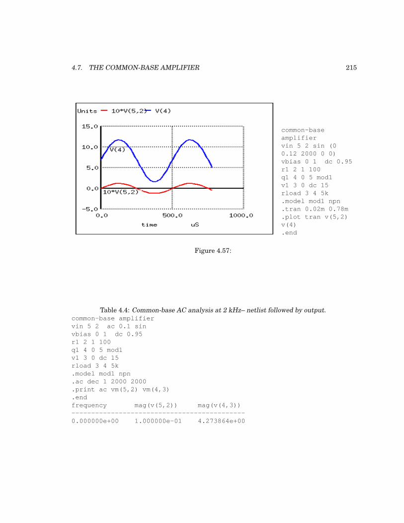
4.7. THE COMMON-BASE AMPLIFIER 215
common-baseamplifiervin 5 2 sin (00.12 2000 0 0)vbias 0 1 dc 0.95r1 2 1 100q1 4 0 5 mod1v1 3 0 dc 15rload 3 4 5k.model mod1 npn.tran 0.02m 0.78m.plot tran v(5,2)v(4).end
Figure 4.57:
Table 4.4: Common-base AC analysis at 2 kHz– netlist followed by output.common-base amplifiervin 5 2 ac 0.1 sinvbias 0 1 dc 0.95r1 2 1 100q1 4 0 5 mod1v1 3 0 dc 15rload 3 4 5k.model mod1 npn.ac dec 1 2000 2000.print ac vm(5,2) vm(4,3).endfrequency mag(v(5,2)) mag(v(4,3))--------------------------------------------0.000000e+00 1.000000e-01 4.273864e+00
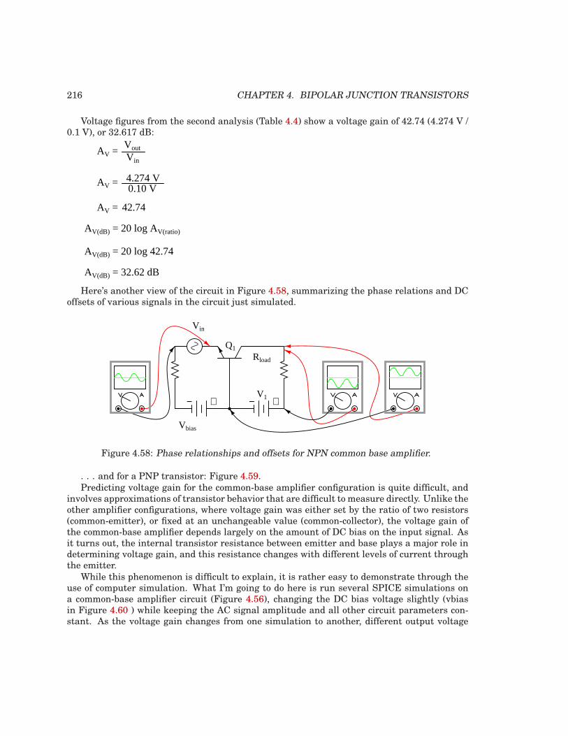
216 CHAPTER 4. BIPOLAR JUNCTION TRANSISTORS
Voltage figures from the second analysis (Table 4.4) show a voltage gain of 42.74 (4.274 V /0.1 V), or 32.617 dB:
AV = Vout
Vin
AV =
AV =
AV(dB) = 20 log AV(ratio)
4.274 V0.10 V
42.74
AV(dB) = 20 log 42.74
AV(dB) = 32.62 dB
Here’s another view of the circuit in Figure 4.58, summarizing the phase relations and DCoffsets of various signals in the circuit just simulated.
Rload
Vbias
+−+−V1
Q1
Vin
Figure 4.58: Phase relationships and offsets for NPN common base amplifier.
. . . and for a PNP transistor: Figure 4.59.Predicting voltage gain for the common-base amplifier configuration is quite difficult, and
involves approximations of transistor behavior that are difficult to measure directly. Unlike theother amplifier configurations, where voltage gain was either set by the ratio of two resistors(common-emitter), or fixed at an unchangeable value (common-collector), the voltage gain ofthe common-base amplifier depends largely on the amount of DC bias on the input signal. Asit turns out, the internal transistor resistance between emitter and base plays a major role indetermining voltage gain, and this resistance changes with different levels of current throughthe emitter.
While this phenomenon is difficult to explain, it is rather easy to demonstrate through theuse of computer simulation. What I’m going to do here is run several SPICE simulations ona common-base amplifier circuit (Figure 4.56), changing the DC bias voltage slightly (vbiasin Figure 4.60 ) while keeping the AC signal amplitude and all other circuit parameters con-stant. As the voltage gain changes from one simulation to another, different output voltage
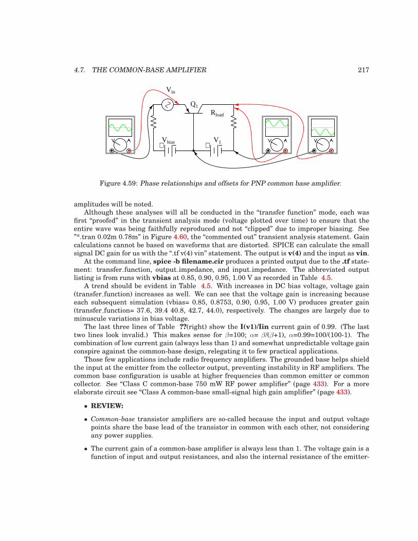
4.7. THE COMMON-BASE AMPLIFIER 217
Rload
Vbias+ −V1
Q1
Vin
+ −
Figure 4.59: Phase relationships and offsets for PNP common base amplifier.
amplitudes will be noted.Although these analyses will all be conducted in the “transfer function” mode, each was
first “proofed” in the transient analysis mode (voltage plotted over time) to ensure that theentire wave was being faithfully reproduced and not “clipped” due to improper biasing. See”*.tran 0.02m 0.78m” in Figure 4.60, the “commented out” transient analysis statement. Gaincalculations cannot be based on waveforms that are distorted. SPICE can calculate the smallsignal DC gain for us with the “.tf v(4) vin” statement. The output is v(4) and the input as vin.
At the command line, spice -b filename.cir produces a printed output due to the .tf state-ment: transfer function, output impedance, and input impedance. The abbreviated outputlisting is from runs with vbias at 0.85, 0.90, 0.95, 1.00 V as recorded in Table 4.5.
A trend should be evident in Table 4.5. With increases in DC bias voltage, voltage gain(transfer function) increases as well. We can see that the voltage gain is increasing becauseeach subsequent simulation (vbias= 0.85, 0.8753, 0.90, 0.95, 1.00 V) produces greater gain(transfer function= 37.6, 39.4 40.8, 42.7, 44.0), respectively. The changes are largely due tominuscule variations in bias voltage.
The last three lines of Table ??(right) show the I(v1)/Iin current gain of 0.99. (The lasttwo lines look invalid.) This makes sense for β=100; α= β/(β+1), α=0.99=100/(100-1). Thecombination of low current gain (always less than 1) and somewhat unpredictable voltage gainconspire against the common-base design, relegating it to few practical applications.
Those few applications include radio frequency amplifiers. The grounded base helps shieldthe input at the emitter from the collector output, preventing instability in RF amplifiers. Thecommon base configuration is usable at higher frequencies than common emitter or commoncollector. See “Class C common-base 750 mW RF power amplifier” (page 433). For a moreelaborate circuit see “Class A common-base small-signal high gain amplifier” (page 433).
• REVIEW:
• Common-base transistor amplifiers are so-called because the input and output voltagepoints share the base lead of the transistor in common with each other, not consideringany power supplies.
• The current gain of a common-base amplifier is always less than 1. The voltage gain is afunction of input and output resistances, and also the internal resistance of the emitter-
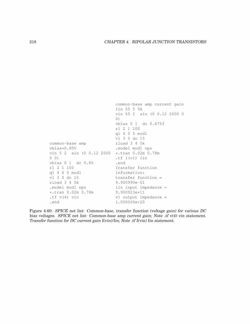
218 CHAPTER 4. BIPOLAR JUNCTION TRANSISTORS
common-base ampvbias=0.85Vvin 5 2 sin (0 0.12 20000 0)vbias 0 1 dc 0.85r1 2 1 100q1 4 0 5 mod1v1 3 0 dc 15rload 3 4 5k.model mod1 npn
* .tran 0.02m 0.78m.tf v(4) vin.end
common-base amp current gainIin 55 5 0Avin 55 2 sin (0 0.12 2000 00)vbias 0 1 dc 0.8753r1 2 1 100q1 4 0 5 mod1v1 3 0 dc 15rload 3 4 5k.model mod1 npn
* .tran 0.02m 0.78m.tf I(v1) Iin.endTransfer functioninformation:transfer function =9.900990e-01iin input impedance =9.900923e+11v1 output impedance =1.000000e+20
Figure 4.60: SPICE net list: Common-base, transfer function (voltage gain) for various DCbias voltages. SPICE net list: Common-base amp current gain; Note .tf v(4) vin statement.Transfer function for DC current gain I(vin)/Iin; Note .tf I(vin) Iin statement.

4.7. THE COMMON-BASE AMPLIFIER 219
Table 4.5: SPICE output: Common-base transfer function.Circuit: common-base amp vbias=0.85Vtransfer function = 3.756565e+01output impedance at v(4) = 5.000000e+03vin#input impedance = 1.317825e+02
Circuit: common-base amp vbias=0.8753V Ic=1 mATransfer function information:transfer function = 3.942567e+01output impedance at v(4) = 5.000000e+03vin#input impedance = 1.255653e+02
Circuit: common-base amp vbias=0.9Vtransfer function = 4.079542e+01output impedance at v(4) = 5.000000e+03vin#input impedance = 1.213493e+02
Circuit: common-base amp vbias=0.95Vtransfer function = 4.273864e+01output impedance at v(4) = 5.000000e+03vin#input impedance = 1.158318e+02
Circuit: common-base amp vbias=1.00Vtransfer function = 4.401137e+01output impedance at v(4) = 5.000000e+03vin#input impedance = 1.124822e+02
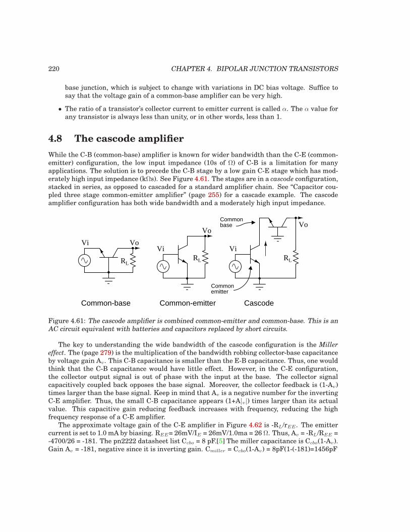
220 CHAPTER 4. BIPOLAR JUNCTION TRANSISTORS
base junction, which is subject to change with variations in DC bias voltage. Suffice tosay that the voltage gain of a common-base amplifier can be very high.
• The ratio of a transistor’s collector current to emitter current is called α. The α value forany transistor is always less than unity, or in other words, less than 1.
4.8 The cascode amplifier
While the C-B (common-base) amplifier is known for wider bandwidth than the C-E (common-emitter) configuration, the low input impedance (10s of Ω) of C-B is a limitation for manyapplications. The solution is to precede the C-B stage by a low gain C-E stage which has mod-erately high input impedance (kΩs). See Figure 4.61. The stages are in a cascode configuration,stacked in series, as opposed to cascaded for a standard amplifier chain. See “Capacitor cou-pled three stage common-emitter amplifier” (page 255) for a cascade example. The cascodeamplifier configuration has both wide bandwidth and a moderately high input impedance.
RLRL
ViVoVi
Vo
RL
Vi
Vo
Common-base Common-emitter Cascode
Commonemitter
Commonbase
Figure 4.61: The cascode amplifier is combined common-emitter and common-base. This is anAC circuit equivalent with batteries and capacitors replaced by short circuits.
The key to understanding the wide bandwidth of the cascode configuration is the Miller
effect. The (page 279) is the multiplication of the bandwidth robbing collector-base capacitanceby voltage gain Av. This C-B capacitance is smaller than the E-B capacitance. Thus, one wouldthink that the C-B capacitance would have little effect. However, in the C-E configuration,the collector output signal is out of phase with the input at the base. The collector signalcapacitively coupled back opposes the base signal. Moreover, the collector feedback is (1-Av)times larger than the base signal. Keep in mind that Av is a negative number for the invertingC-E amplifier. Thus, the small C-B capacitance appears (1+A|v|) times larger than its actualvalue. This capacitive gain reducing feedback increases with frequency, reducing the highfrequency response of a C-E amplifier.
The approximate voltage gain of the C-E amplifier in Figure 4.62 is -RL/rEE . The emittercurrent is set to 1.0 mA by biasing. REE= 26mV/IE = 26mV/1.0ma = 26 Ω. Thus, Av = -RL/REE =-4700/26 = -181. The pn2222 datasheet list Ccbo = 8 pF.[5] The miller capacitance is Ccbo(1-Av).Gain Av = -181, negative since it is inverting gain. Cmiller = Ccbo(1-Av) = 8pF(1-(-181)=1456pF
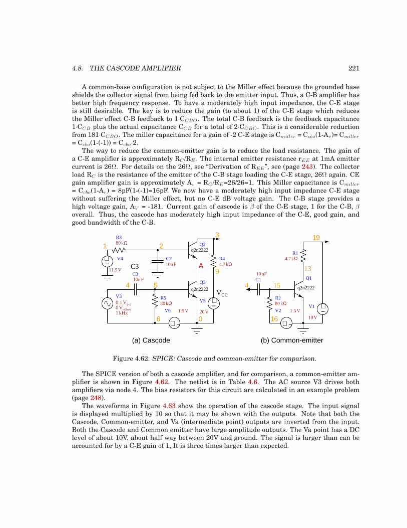
4.8. THE CASCODE AMPLIFIER 221
A common-base configuration is not subject to the Miller effect because the grounded baseshields the collector signal from being fed back to the emitter input. Thus, a C-B amplifier hasbetter high frequency response. To have a moderately high input impedance, the C-E stageis still desirable. The key is to reduce the gain (to about 1) of the C-E stage which reducesthe Miller effect C-B feedback to 1·CCBO. The total C-B feedback is the feedback capacitance1·CCB plus the actual capacitance CCB for a total of 2·CCBO. This is a considerable reductionfrom 181·CCBO. The miller capacitance for a gain of -2 C-E stage is Cmiller = Ccbo(1-Av)= Cmiller
= Ccbo(1-(-1)) = Ccbo·2.The way to reduce the common-emitter gain is to reduce the load resistance. The gain of
a C-E amplifier is approximately RC /RE . The internal emitter resistance rEE at 1mA emittercurrent is 26Ω. For details on the 26Ω, see “Derivation of REE”, see (page 243). The collectorload RC is the resistance of the emitter of the C-B stage loading the C-E stage, 26Ω again. CEgain amplifier gain is approximately Av = RC /RE=26/26=1. This Miller capacitance is Cmiller
= Ccbo(1-Av) = 8pF(1-(-1)=16pF. We now have a moderately high input impedance C-E stagewithout suffering the Miller effect, but no C-E dB voltage gain. The C-B stage provides ahigh voltage gain, AV = -181. Current gain of cascode is β of the C-E stage, 1 for the C-B, β
overall. Thus, the cascode has moderately high input impedance of the C-E, good gain, andgood bandwidth of the C-B.
VCC
+ −1.5 VV6
+−
20V
V5
+−11.5V
V4
80kΩR5
10n FC3
10n FC2
1 23
4 5
6
94.7 kΩR4
80 kΩR3
Α
0.1 Vp-p0 Voffset1 kHz
V3
C3
80kΩR2
10 nFC1
+ −1.5 VV2
4.7 kΩR1
13
154
16
+−
10V
V1
19
(b) Common-emitter(a) Cascode
q2n2222Q2
q2n2222
Q3q2n2222
Q1
0
Figure 4.62: SPICE: Cascode and common-emitter for comparison.
The SPICE version of both a cascode amplifier, and for comparison, a common-emitter am-plifier is shown in Figure 4.62. The netlist is in Table 4.6. The AC source V3 drives bothamplifiers via node 4. The bias resistors for this circuit are calculated in an example problem(page 248).
The waveforms in Figure 4.63 show the operation of the cascode stage. The input signalis displayed multiplied by 10 so that it may be shown with the outputs. Note that both theCascode, Common-emitter, and Va (intermediate point) outputs are inverted from the input.Both the Cascode and Common emitter have large amplitude outputs. The Va point has a DClevel of about 10V, about half way between 20V and ground. The signal is larger than can beaccounted for by a C-E gain of 1, It is three times larger than expected.
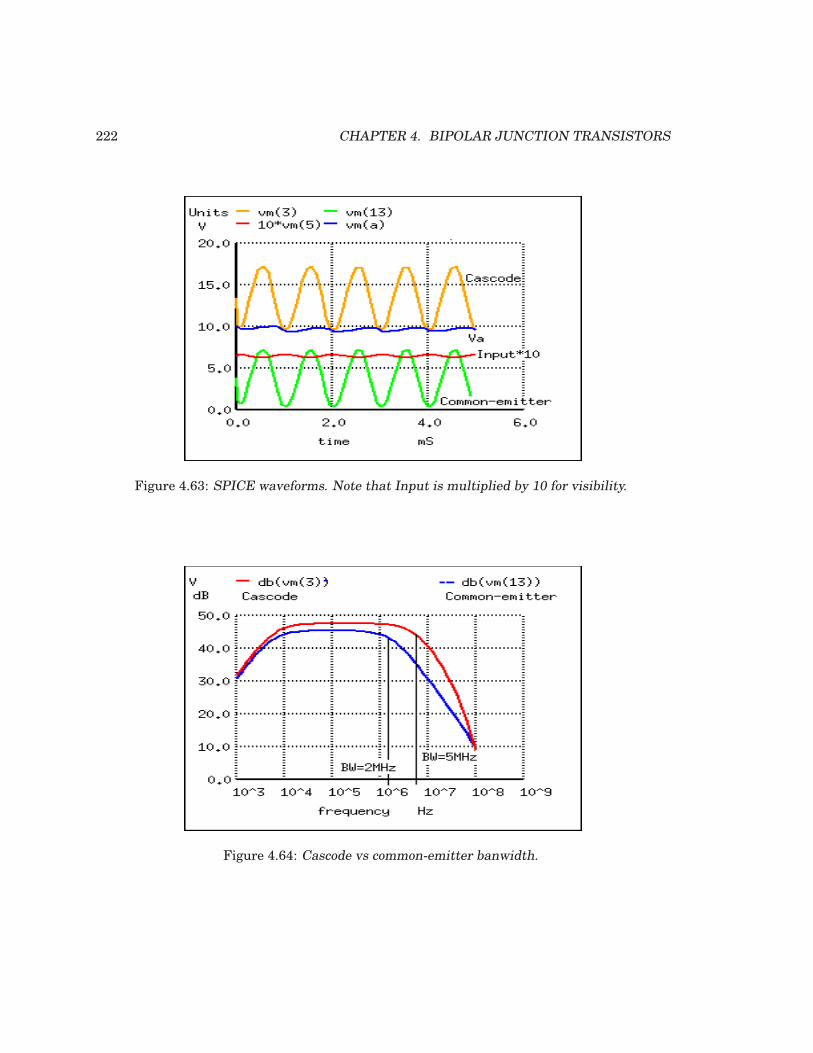
222 CHAPTER 4. BIPOLAR JUNCTION TRANSISTORS
Figure 4.63: SPICE waveforms. Note that Input is multiplied by 10 for visibility.
Figure 4.64: Cascode vs common-emitter banwidth.

4.8. THE CASCODE AMPLIFIER 223
Table 4.6: SPICE netlist for printing AC input and output voltages.
* SPICE circuit <03502.eps> from XCircuit v3.20V1 19 0 10Q1 13 15 0 q2n2222Q2 3 2 A q2n2222R1 19 13 4.7kV2 16 0 1.5C1 4 15 10nR2 15 16 80kQ3 A 5 0 q2n2222V3 4 6 SIN(0 0.1 1k) ac 1R3 1 2 80kR4 3 9 4.7kC2 2 0 10nC3 4 5 10nR5 5 6 80kV4 1 0 11.5V5 9 0 20V6 6 0 1.5.model q2n2222 npn (is=19f bf=150+ vaf=100 ikf=0.18 ise=50p ne=2.5 br=7.5+ var=6.4 ikr=12m isc=8.7p nc=1.2 rb=50+ re=0.4 rc=0.3 cje=26p tf=0.5n+ cjc=11p tr=7n xtb=1.5 kf=0.032f af=1).tran 1u 5m.AC DEC 10 1k 100Meg.end
224 CHAPTER 4. BIPOLAR JUNCTION TRANSISTORS
Figure 4.64 shows the frequency response to both the cascode and common-emitter ampli-fiers. The SPICE statements responsible for the AC analysis, extracted from the listing:
V3 4 6 SIN(0 0.1 1k) ac 1.AC DEC 10 1k 100Meg
Note the “ac 1” is necessary at the end of the V3 statement. The cascode has marginallybetter mid-band gain. However, we are primarily looking for the bandwidth measured at the-3dB points, down from the midband gain for each amplifier. This is shown by the vertical solidlines in Figure 4.64. It is also possible to print the data of interest from nutmeg to the screen,the SPICE graphical viewer (command, first line):
nutmeg 6 -> print frequency db(vm(3)) db(vm(13))Index frequency db(vm(3)) db(vm(13))22 0.158MHz 47.54 45.4133 1.995MHz 46.95 42.0637 5.012MHz 44.63 36.17
Index 22 gives the midband dB gain for Cascode vm(3)=47.5dB and Common-emitter vm(13)=45.4dB.Out of many printed lines, Index 33 was the closest to being 3dB down from 45.4dB at 42.0dBfor the Common-emitter circuit. The corresponding Index 33 frequency is approximately 2Mhz,the common-emitter bandwidth. Index 37 vm(3)=44.6db is approximately 3db down from47.5db. The corresponding Index37 frequency is 5Mhz, the cascode bandwidth. Thus, thecascode amplifier has a wider bandwidth. We are not concerned with the low frequency degra-dation of gain. It is due to the capacitors, which could be remedied with larger ones.
The 5MHz bandwith of our cascode example, while better than the common-emitter ex-ample, is not exemplary for an RF (radio frequency) amplifier. A pair of RF or microwavetransistors with lower interelectrode capacitances should be used for higher bandwidth. Be-fore the invention of the RF dual gate MOSFET, the BJT cascode amplifier could have beenfound in UHF (ultra high frequency) TV tuners.
• REVIEW
• A cascode amplifier consists of a common-emitter stage loaded by the emitter of a common-base stage.
• The heavily loaded C-E stage has a low gain of 1, overcoming the Miller effect
• A cascode amplifier has a high gain, moderately high input impedance, a high outputimpedance, and a high bandwidth.
4.9 Biasing techniques
In the common-emitter section of this chapter, we saw a SPICE analysis where the outputwaveform resembled a half-wave rectified shape: only half of the input waveform was repro-duced, with the other half being completely cut off. Since our purpose at that time was toreproduce the entire waveshape, this constituted a problem. The solution to this problem was
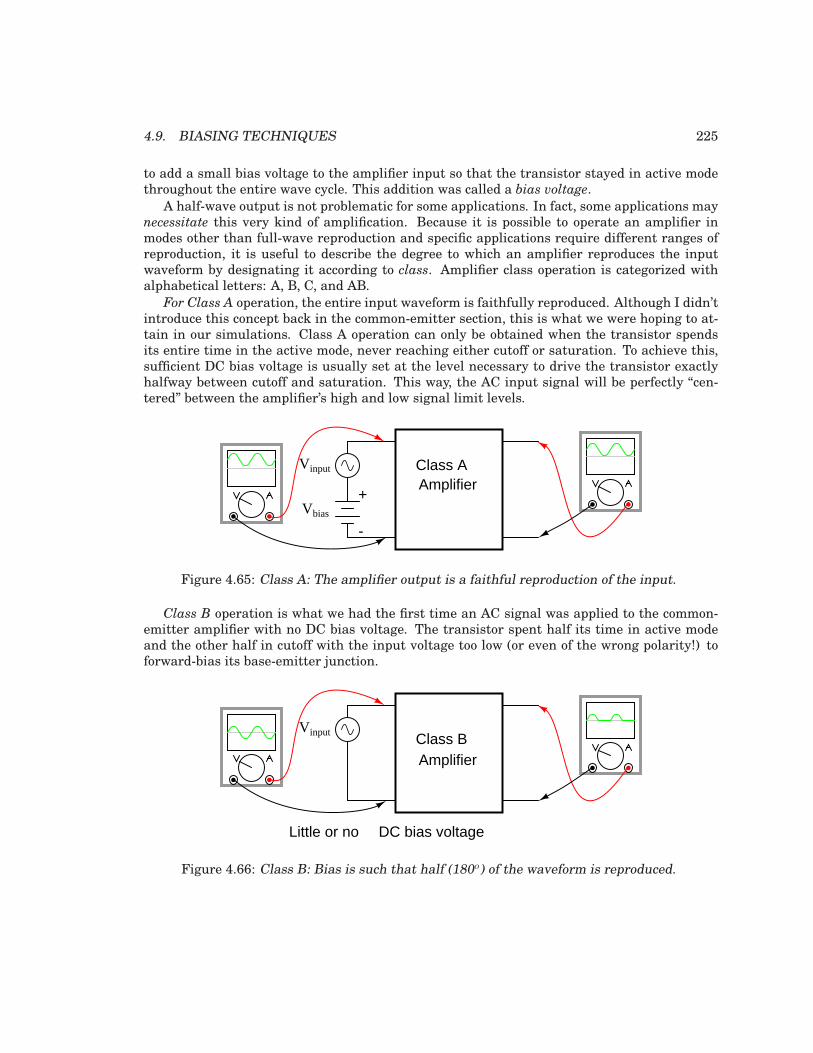
4.9. BIASING TECHNIQUES 225
to add a small bias voltage to the amplifier input so that the transistor stayed in active modethroughout the entire wave cycle. This addition was called a bias voltage.
A half-wave output is not problematic for some applications. In fact, some applications maynecessitate this very kind of amplification. Because it is possible to operate an amplifier inmodes other than full-wave reproduction and specific applications require different ranges ofreproduction, it is useful to describe the degree to which an amplifier reproduces the inputwaveform by designating it according to class. Amplifier class operation is categorized withalphabetical letters: A, B, C, and AB.
For Class A operation, the entire input waveform is faithfully reproduced. Although I didn’tintroduce this concept back in the common-emitter section, this is what we were hoping to at-tain in our simulations. Class A operation can only be obtained when the transistor spendsits entire time in the active mode, never reaching either cutoff or saturation. To achieve this,sufficient DC bias voltage is usually set at the level necessary to drive the transistor exactlyhalfway between cutoff and saturation. This way, the AC input signal will be perfectly “cen-tered” between the amplifier’s high and low signal limit levels.
Vinput
Vbias
AmplifierClass A
-
+
Figure 4.65: Class A: The amplifier output is a faithful reproduction of the input.
Class B operation is what we had the first time an AC signal was applied to the common-emitter amplifier with no DC bias voltage. The transistor spent half its time in active modeand the other half in cutoff with the input voltage too low (or even of the wrong polarity!) toforward-bias its base-emitter junction.
Vinput
AmplifierClass B
Little or no DC bias voltage
Figure 4.66: Class B: Bias is such that half (180o) of the waveform is reproduced.
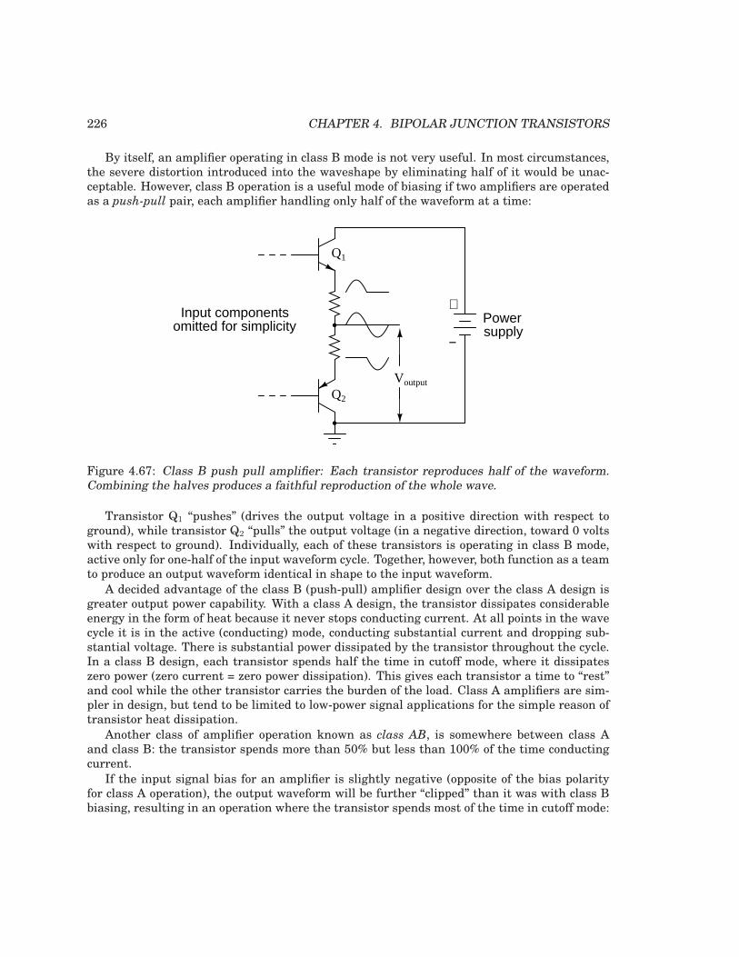
226 CHAPTER 4. BIPOLAR JUNCTION TRANSISTORS
By itself, an amplifier operating in class B mode is not very useful. In most circumstances,the severe distortion introduced into the waveshape by eliminating half of it would be unac-ceptable. However, class B operation is a useful mode of biasing if two amplifiers are operatedas a push-pull pair, each amplifier handling only half of the waveform at a time:
Voutput
Input componentsomitted for simplicity
Powersupply
Q1
Q2
+
−
Figure 4.67: Class B push pull amplifier: Each transistor reproduces half of the waveform.Combining the halves produces a faithful reproduction of the whole wave.
Transistor Q1 “pushes” (drives the output voltage in a positive direction with respect toground), while transistor Q2 “pulls” the output voltage (in a negative direction, toward 0 voltswith respect to ground). Individually, each of these transistors is operating in class B mode,active only for one-half of the input waveform cycle. Together, however, both function as a teamto produce an output waveform identical in shape to the input waveform.
A decided advantage of the class B (push-pull) amplifier design over the class A design isgreater output power capability. With a class A design, the transistor dissipates considerableenergy in the form of heat because it never stops conducting current. At all points in the wavecycle it is in the active (conducting) mode, conducting substantial current and dropping sub-stantial voltage. There is substantial power dissipated by the transistor throughout the cycle.In a class B design, each transistor spends half the time in cutoff mode, where it dissipateszero power (zero current = zero power dissipation). This gives each transistor a time to “rest”and cool while the other transistor carries the burden of the load. Class A amplifiers are sim-pler in design, but tend to be limited to low-power signal applications for the simple reason oftransistor heat dissipation.
Another class of amplifier operation known as class AB, is somewhere between class Aand class B: the transistor spends more than 50% but less than 100% of the time conductingcurrent.
If the input signal bias for an amplifier is slightly negative (opposite of the bias polarityfor class A operation), the output waveform will be further “clipped” than it was with class Bbiasing, resulting in an operation where the transistor spends most of the time in cutoff mode:
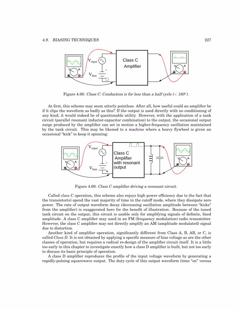
4.9. BIASING TECHNIQUES 227
Vinput Class C
Vbias
-
+
Amplifier
Figure 4.68: Class C: Conduction is for less than a half cycle (< 180o).
At first, this scheme may seem utterly pointless. After all, how useful could an amplifier beif it clips the waveform as badly as this? If the output is used directly with no conditioning ofany kind, it would indeed be of questionable utility. However, with the application of a tankcircuit (parallel resonant inductor-capacitor combination) to the output, the occasional outputsurge produced by the amplifier can set in motion a higher-frequency oscillation maintainedby the tank circuit. This may be likened to a machine where a heavy flywheel is given anoccasional “kick” to keep it spinning:
Vinput
AmplifierClass C
Vbias
with resonant output
-
+
Figure 4.69: Class C amplifier driving a resonant circuit.
Called class C operation, this scheme also enjoys high power efficiency due to the fact thatthe transistor(s) spend the vast majority of time in the cutoff mode, where they dissipate zeropower. The rate of output waveform decay (decreasing oscillation amplitude between “kicks”from the amplifier) is exaggerated here for the benefit of illustration. Because of the tunedtank circuit on the output, this circuit is usable only for amplifying signals of definite, fixedamplitude. A class C amplifier may used in an FM (frequency modulation) radio transmitter.However, the class C amplifier may not directly amplify an AM (amplitude modulated) signaldue to distortion.
Another kind of amplifier operation, significantly different from Class A, B, AB, or C, iscalled Class D. It is not obtained by applying a specific measure of bias voltage as are the otherclasses of operation, but requires a radical re-design of the amplifier circuit itself. It is a littletoo early in this chapter to investigate exactly how a class D amplifier is built, but not too earlyto discuss its basic principle of operation.
A class D amplifier reproduces the profile of the input voltage waveform by generating arapidly-pulsing squarewave output. The duty cycle of this output waveform (time “on” versus
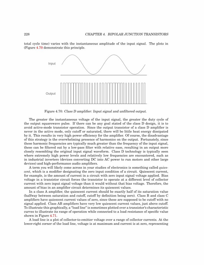
228 CHAPTER 4. BIPOLAR JUNCTION TRANSISTORS
total cycle time) varies with the instantaneous amplitude of the input signal. The plots in(Figure 4.70 demonstrate this principle.
Input
Output
Figure 4.70: Class D amplifier: Input signal and unfiltered output.
The greater the instantaneous voltage of the input signal, the greater the duty cycle ofthe output squarewave pulse. If there can be any goal stated of the class D design, it is toavoid active-mode transistor operation. Since the output transistor of a class D amplifier isnever in the active mode, only cutoff or saturated, there will be little heat energy dissipatedby it. This results in very high power efficiency for the amplifier. Of course, the disadvantageof this strategy is the overwhelming presence of harmonics on the output. Fortunately, sincethese harmonic frequencies are typically much greater than the frequency of the input signal,these can be filtered out by a low-pass filter with relative ease, resulting in an output moreclosely resembling the original input signal waveform. Class D technology is typically seenwhere extremely high power levels and relatively low frequencies are encountered, such asin industrial inverters (devices converting DC into AC power to run motors and other largedevices) and high-performance audio amplifiers.
A term you will likely come across in your studies of electronics is something called quies-
cent, which is a modifier designating the zero input condition of a circuit. Quiescent current,for example, is the amount of current in a circuit with zero input signal voltage applied. Biasvoltage in a transistor circuit forces the transistor to operate at a different level of collectorcurrent with zero input signal voltage than it would without that bias voltage. Therefore, theamount of bias in an amplifier circuit determines its quiescent values.
In a class A amplifier, the quiescent current should be exactly half of its saturation value(halfway between saturation and cutoff, cutoff by definition being zero). Class B and class Camplifiers have quiescent current values of zero, since these are supposed to be cutoff with nosignal applied. Class AB amplifiers have very low quiescent current values, just above cutoff.To illustrate this graphically, a “load line” is sometimes plotted over a transistor’s characteristiccurves to illustrate its range of operation while connected to a load resistance of specific valueshown in Figure 4.71.
A load line is a plot of collector-to-emitter voltage over a range of collector currents. At thelower-right corner of the load line, voltage is at maximum and current is at zero, representing
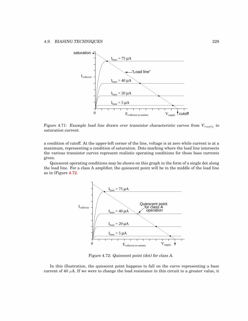
4.9. BIASING TECHNIQUES 229
Icollector
Ecollector-to-emitter
"Load line"
Vsupply0
Ibase = 75 µA
Ibase = 40 µA
Ibase = 20 µA
Ibase = 5 µA
cutoff
saturation
Figure 4.71: Example load line drawn over transistor characteristic curves from Vsupply tosaturation current.
a condition of cutoff. At the upper-left corner of the line, voltage is at zero while current is at amaximum, representing a condition of saturation. Dots marking where the load line intersectsthe various transistor curves represent realistic operating conditions for those base currentsgiven.
Quiescent operating conditions may be shown on this graph in the form of a single dot alongthe load line. For a class A amplifier, the quiescent point will be in the middle of the load lineas in (Figure 4.72.
Icollector
Ecollector-to-emitterVsupply0
Quiescent pointfor class A operation
Ibase = 75 µA
Ibase = 40 µA
Ibase = 20 µA
Ibase = 5 µA
Figure 4.72: Quiescent point (dot) for class A.
In this illustration, the quiescent point happens to fall on the curve representing a basecurrent of 40 µA. If we were to change the load resistance in this circuit to a greater value, it
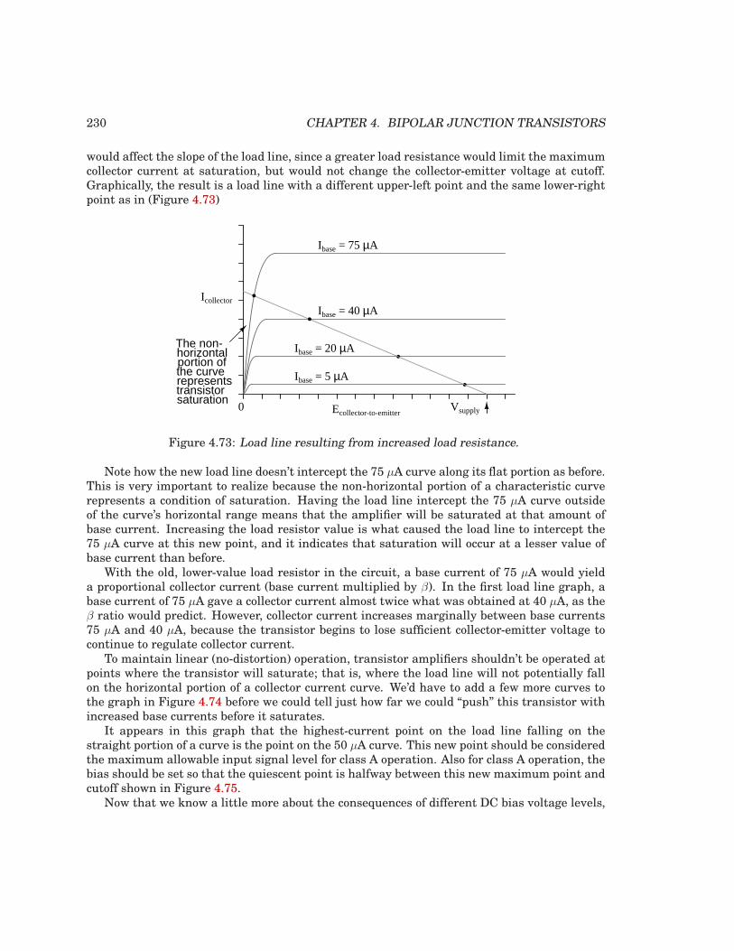
230 CHAPTER 4. BIPOLAR JUNCTION TRANSISTORS
would affect the slope of the load line, since a greater load resistance would limit the maximumcollector current at saturation, but would not change the collector-emitter voltage at cutoff.Graphically, the result is a load line with a different upper-left point and the same lower-rightpoint as in (Figure 4.73)
Icollector
Ecollector-to-emitterVsupply0
Ibase = 75 µA
Ibase = 40 µA
Ibase = 20 µA
Ibase = 5 µA
The non-horizontalportion ofthe curverepresentstransistorsaturation
Figure 4.73: Load line resulting from increased load resistance.
Note how the new load line doesn’t intercept the 75 µA curve along its flat portion as before.This is very important to realize because the non-horizontal portion of a characteristic curverepresents a condition of saturation. Having the load line intercept the 75 µA curve outsideof the curve’s horizontal range means that the amplifier will be saturated at that amount ofbase current. Increasing the load resistor value is what caused the load line to intercept the75 µA curve at this new point, and it indicates that saturation will occur at a lesser value ofbase current than before.
With the old, lower-value load resistor in the circuit, a base current of 75 µA would yielda proportional collector current (base current multiplied by β). In the first load line graph, abase current of 75 µA gave a collector current almost twice what was obtained at 40 µA, as theβ ratio would predict. However, collector current increases marginally between base currents75 µA and 40 µA, because the transistor begins to lose sufficient collector-emitter voltage tocontinue to regulate collector current.
To maintain linear (no-distortion) operation, transistor amplifiers shouldn’t be operated atpoints where the transistor will saturate; that is, where the load line will not potentially fallon the horizontal portion of a collector current curve. We’d have to add a few more curves tothe graph in Figure 4.74 before we could tell just how far we could “push” this transistor withincreased base currents before it saturates.
It appears in this graph that the highest-current point on the load line falling on thestraight portion of a curve is the point on the 50 µA curve. This new point should be consideredthe maximum allowable input signal level for class A operation. Also for class A operation, thebias should be set so that the quiescent point is halfway between this new maximum point andcutoff shown in Figure 4.75.
Now that we know a little more about the consequences of different DC bias voltage levels,
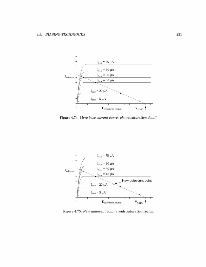
4.9. BIASING TECHNIQUES 231
Icollector
Ecollector-to-emitter Vsupply0
Ibase = 50 µA
Ibase = 40 µA
Ibase = 75 µA
Ibase = 20 µA
Ibase = 5 µA
Ibase = 60 µA
Figure 4.74: More base current curves shows saturation detail.
Icollector
Ecollector-to-emitter Vsupply0
Ibase = 50 µA
Ibase = 40 µA
Ibase = 75 µA
Ibase = 20 µA
Ibase = 5 µA
Ibase = 60 µA
New quiescent point
Figure 4.75: New quiescent point avoids saturation region.
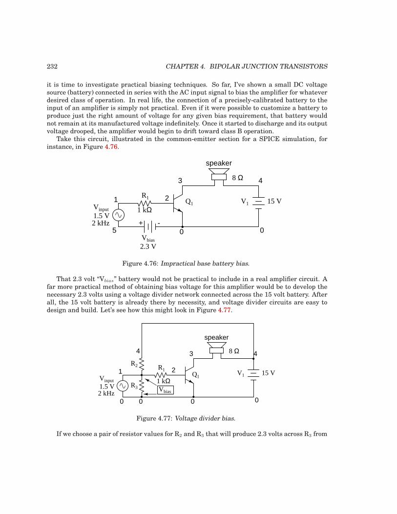
232 CHAPTER 4. BIPOLAR JUNCTION TRANSISTORS
it is time to investigate practical biasing techniques. So far, I’ve shown a small DC voltagesource (battery) connected in series with the AC input signal to bias the amplifier for whateverdesired class of operation. In real life, the connection of a precisely-calibrated battery to theinput of an amplifier is simply not practical. Even if it were possible to customize a battery toproduce just the right amount of voltage for any given bias requirement, that battery wouldnot remain at its manufactured voltage indefinitely. Once it started to discharge and its outputvoltage drooped, the amplifier would begin to drift toward class B operation.
Take this circuit, illustrated in the common-emitter section for a SPICE simulation, forinstance, in Figure 4.76.
speaker
V1 15 VQ1
R1
1 kΩ
8 Ω
1
0 0
2
3 4
Vinput
1.5 V2 kHz
Vbias
5
2.3 V
+ -
Figure 4.76: Impractical base battery bias.
That 2.3 volt “Vbias” battery would not be practical to include in a real amplifier circuit. Afar more practical method of obtaining bias voltage for this amplifier would be to develop thenecessary 2.3 volts using a voltage divider network connected across the 15 volt battery. Afterall, the 15 volt battery is already there by necessity, and voltage divider circuits are easy todesign and build. Let’s see how this might look in Figure 4.77.
speaker
V1 15 VQ1
R1
1 kΩ
8 Ω
1
0 0
2
3 4
Vinput
1.5 V2 kHz
Vbias
4
0
R2
R3
0
Figure 4.77: Voltage divider bias.
If we choose a pair of resistor values for R2 and R3 that will produce 2.3 volts across R3 from
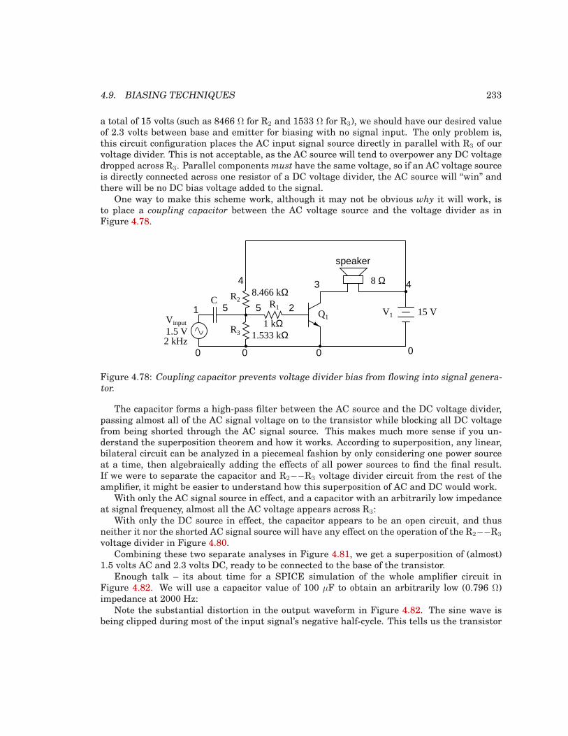
4.9. BIASING TECHNIQUES 233
a total of 15 volts (such as 8466 Ω for R2 and 1533 Ω for R3), we should have our desired valueof 2.3 volts between base and emitter for biasing with no signal input. The only problem is,this circuit configuration places the AC input signal source directly in parallel with R3 of ourvoltage divider. This is not acceptable, as the AC source will tend to overpower any DC voltagedropped across R3. Parallel componentsmust have the same voltage, so if an AC voltage sourceis directly connected across one resistor of a DC voltage divider, the AC source will “win” andthere will be no DC bias voltage added to the signal.
One way to make this scheme work, although it may not be obvious why it will work, isto place a coupling capacitor between the AC voltage source and the voltage divider as inFigure 4.78.
speaker
V1 15 VQ1
R1
1 kΩ
8 Ω
1
0 0
2
3 4
Vinput
1.5 V2 kHz
4
0
R2
R3
0
5C
5
8.466 kΩ
1.533 kΩ
Figure 4.78: Coupling capacitor prevents voltage divider bias from flowing into signal genera-tor.
The capacitor forms a high-pass filter between the AC source and the DC voltage divider,passing almost all of the AC signal voltage on to the transistor while blocking all DC voltagefrom being shorted through the AC signal source. This makes much more sense if you un-derstand the superposition theorem and how it works. According to superposition, any linear,bilateral circuit can be analyzed in a piecemeal fashion by only considering one power sourceat a time, then algebraically adding the effects of all power sources to find the final result.If we were to separate the capacitor and R2−−R3 voltage divider circuit from the rest of theamplifier, it might be easier to understand how this superposition of AC and DC would work.
With only the AC signal source in effect, and a capacitor with an arbitrarily low impedanceat signal frequency, almost all the AC voltage appears across R3:
With only the DC source in effect, the capacitor appears to be an open circuit, and thusneither it nor the shorted AC signal source will have any effect on the operation of the R2−−R3
voltage divider in Figure 4.80.Combining these two separate analyses in Figure 4.81, we get a superposition of (almost)
1.5 volts AC and 2.3 volts DC, ready to be connected to the base of the transistor.Enough talk – its about time for a SPICE simulation of the whole amplifier circuit in
Figure 4.82. We will use a capacitor value of 100 µF to obtain an arbitrarily low (0.796 Ω)impedance at 2000 Hz:
Note the substantial distortion in the output waveform in Figure 4.82. The sine wave isbeing clipped during most of the input signal’s negative half-cycle. This tells us the transistor
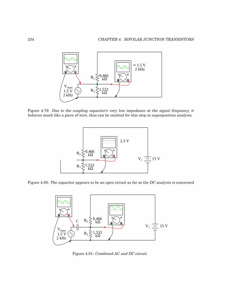
234 CHAPTER 4. BIPOLAR JUNCTION TRANSISTORS
Vinput
1.5 V2 kHz
R2
R31.533
kΩ
8.466kΩ
≈ 1.5 V2 kHz
Figure 4.79: Due to the coupling capacitor’s very low impedance at the signal frequency, itbehaves much like a piece of wire, thus can be omitted for this step in superposition analysis.
R2
R31.533
kΩ
8.466kΩ
V1 15 V
2.3 V
Figure 4.80: The capacitor appears to be an open circuit as far at the DC analysis is concerned
V1 15 VVinput
1.5 V2 kHz
R2
R3
C
1.533kΩ
8.466kΩ
Figure 4.81: Combined AC and DC circuit.
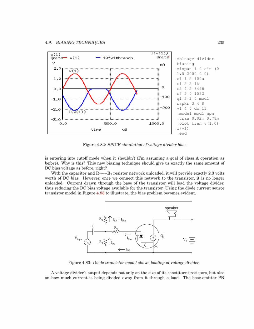
4.9. BIASING TECHNIQUES 235
voltage dividerbiasingvinput 1 0 sin (01.5 2000 0 0)c1 1 5 100ur1 5 2 1kr2 4 5 8466r3 5 0 1533q1 3 2 0 mod1rspkr 3 4 8v1 4 0 dc 15.model mod1 npn.tran 0.02m 0.78m.plot tran v(1,0)i(v1).end
Figure 4.82: SPICE simulation of voltage divider bias.
is entering into cutoff mode when it shouldn’t (I’m assuming a goal of class A operation asbefore). Why is this? This new biasing technique should give us exactly the same amount ofDC bias voltage as before, right?
With the capacitor and R2−−R3 resistor network unloaded, it will provide exactly 2.3 voltsworth of DC bias. However, once we connect this network to the transistor, it is no longerunloaded. Current drawn through the base of the transistor will load the voltage divider,thus reducing the DC bias voltage available for the transistor. Using the diode current sourcetransistor model in Figure 4.83 to illustrate, the bias problem becomes evident.
speaker
V1
Q1
R1
Vinput
R2
R3
C
IR3
Ibias
IR3 + Ibias
IR3
Figure 4.83: Diode transistor model shows loading of voltage divider.
A voltage divider’s output depends not only on the size of its constituent resistors, but alsoon how much current is being divided away from it through a load. The base-emitter PN
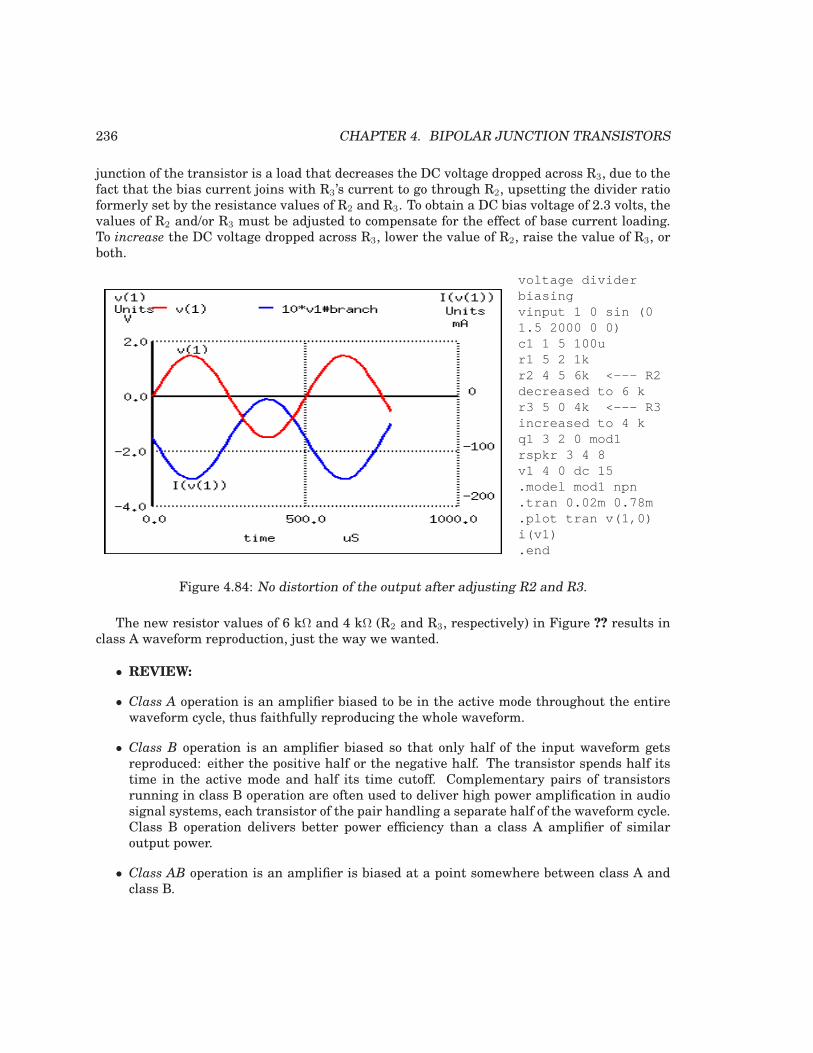
236 CHAPTER 4. BIPOLAR JUNCTION TRANSISTORS
junction of the transistor is a load that decreases the DC voltage dropped across R3, due to thefact that the bias current joins with R3’s current to go through R2, upsetting the divider ratioformerly set by the resistance values of R2 and R3. To obtain a DC bias voltage of 2.3 volts, thevalues of R2 and/or R3 must be adjusted to compensate for the effect of base current loading.To increase the DC voltage dropped across R3, lower the value of R2, raise the value of R3, orboth.
voltage dividerbiasingvinput 1 0 sin (01.5 2000 0 0)c1 1 5 100ur1 5 2 1kr2 4 5 6k <--- R2decreased to 6 kr3 5 0 4k <--- R3increased to 4 kq1 3 2 0 mod1rspkr 3 4 8v1 4 0 dc 15.model mod1 npn.tran 0.02m 0.78m.plot tran v(1,0)i(v1).end
Figure 4.84: No distortion of the output after adjusting R2 and R3.
The new resistor values of 6 kΩ and 4 kΩ (R2 and R3, respectively) in Figure ?? results inclass A waveform reproduction, just the way we wanted.
• REVIEW:
• Class A operation is an amplifier biased to be in the active mode throughout the entirewaveform cycle, thus faithfully reproducing the whole waveform.
• Class B operation is an amplifier biased so that only half of the input waveform getsreproduced: either the positive half or the negative half. The transistor spends half itstime in the active mode and half its time cutoff. Complementary pairs of transistorsrunning in class B operation are often used to deliver high power amplification in audiosignal systems, each transistor of the pair handling a separate half of the waveform cycle.Class B operation delivers better power efficiency than a class A amplifier of similaroutput power.
• Class AB operation is an amplifier is biased at a point somewhere between class A andclass B.
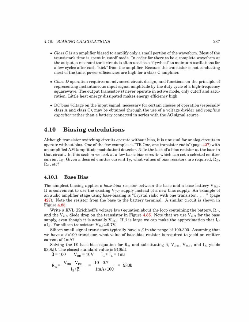
4.10. BIASING CALCULATIONS 237
• Class C is an amplifier biased to amplify only a small portion of the waveform. Most of thetransistor’s time is spent in cutoff mode. In order for there to be a complete waveform atthe output, a resonant tank circuit is often used as a “flywheel” to maintain oscillations fora few cycles after each “kick” from the amplifier. Because the transistor is not conductingmost of the time, power efficiencies are high for a class C amplifier.
• Class D operation requires an advanced circuit design, and functions on the principle ofrepresenting instantaneous input signal amplitude by the duty cycle of a high-frequencysquarewave. The output transistor(s) never operate in active mode, only cutoff and satu-ration. Little heat energy dissipated makes energy efficiency high.
• DC bias voltage on the input signal, necessary for certain classes of operation (especiallyclass A and class C), may be obtained through the use of a voltage divider and coupling
capacitor rather than a battery connected in series with the AC signal source.
4.10 Biasing calculations
Although transistor switching circuits operate without bias, it is unusual for analog circuits tooperate without bias. One of the few examples is “TR One, one transistor radio” (page 427) withan amplified AM (amplitude modulation) detector. Note the lack of a bias resistor at the base inthat circuit. In this section we look at a few basic bias circuits which can set a selected emittercurrent IE . Given a desired emitter current IE , what values of bias resistors are required, RB ,RE , etc?
4.10.1 Base Bias
The simplest biasing applies a base-bias resistor between the base and a base battery VBB .It is convenient to use the existing VCC supply instead of a new bias supply. An example ofan audio amplifier stage using base-biasing is “Crystal radio with one transistor . . . ” (page427). Note the resistor from the base to the battery terminal. A similar circuit is shown inFigure 4.85.
Write a KVL (Krichhoff ’s voltage law) equation about the loop containing the battery, RB ,and the VBE diode drop on the transistor in Figure 4.85. Note that we use VBB for the basesupply, even though it is actually VCC . If β is large we can make the approximation that IC=IE . For silicon transistors VBE
∼=0.7V.
Silicon small signal transistors typically have a β in the range of 100-300. Assuming thatwe have a β=100 transistor, what value of base-bias resistor is required to yield an emittercurrent of 1mA?
Solving the IE base-bias equation for RB and substituting β, VBB , VBE , and IE yields930kΩ. The closest standard value is 910kΩ.
β = 100 IC ≈ IE = 1maVBB = 10V
VBB - VBE
IE /βRB =
10 - 0.7=
1mA/100= 930k
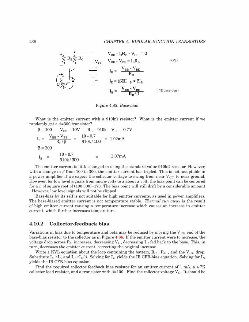
238 CHAPTER 4. BIPOLAR JUNCTION TRANSISTORS
VBE=0.7V
+
_
RCRBVCC
+
_
+_
VBB - VBE = IBRB
VBB - VBE
RBIB =
VBB - IΒRB - VBE = 0
IE = (β+1)ΙΒ ≈ βIB
VBB - VBE
RB /βIE = (IE base-bias)
(KVL)
Figure 4.85: Base-bias
What is the emitter current with a 910kΩ resistor? What is the emitter current if werandomly get a β=300 transistor?
VBB - VBE
RB /βIE =
β = 100 RB = 910kVBB = 10V VBE = 0.7V
10 - 0.7910k / 100=
β = 300
IE =10 - 0.7910k / 300
=
=
1.02mA
3.07mA
The emitter current is little changed in using the standard value 910kΩ resistor. However,with a change in β from 100 to 300, the emitter current has tripled. This is not acceptable ina power amplifier if we expect the collector voltage to swing from near VCC to near ground.However, for low level signals from micro-volts to a about a volt, the bias point can be centeredfor a β of square root of (100·300)=173. The bias point will still drift by a considerable amount. However, low level signals will not be clipped.
Base-bias by its self is not suitable for high emitter currents, as used in power amplifiers.The base-biased emitter current is not temperature stable. Thermal run away is the resultof high emitter current causing a temperature increase which causes an increase in emittercurrent, which further increases temperature.
4.10.2 Collector-feedback bias
Variations in bias due to temperature and beta may be reduced by moving the VBB end of thebase-bias resistor to the collector as in Figure 4.86. If the emitter current were to increase, thevoltage drop across RC increases, decreasing VC , decreasing IB fed back to the base. This, inturn, decreases the emitter current, correcting the original increase.
Write a KVL equation about the loop containing the battery, RC , RB , and the VBE drop.Substitute IC∼=IE and IB∼=IE /β. Solving for IE yields the IE CFB-bias equation. Solving for IByields the IB CFB-bias equation.
Find the required collector feedback bias resistor for an emitter current of 1 mA, a 4.7Kcollector load resistor, and a transistor with β=100 . Find the collector voltage VC . It should be
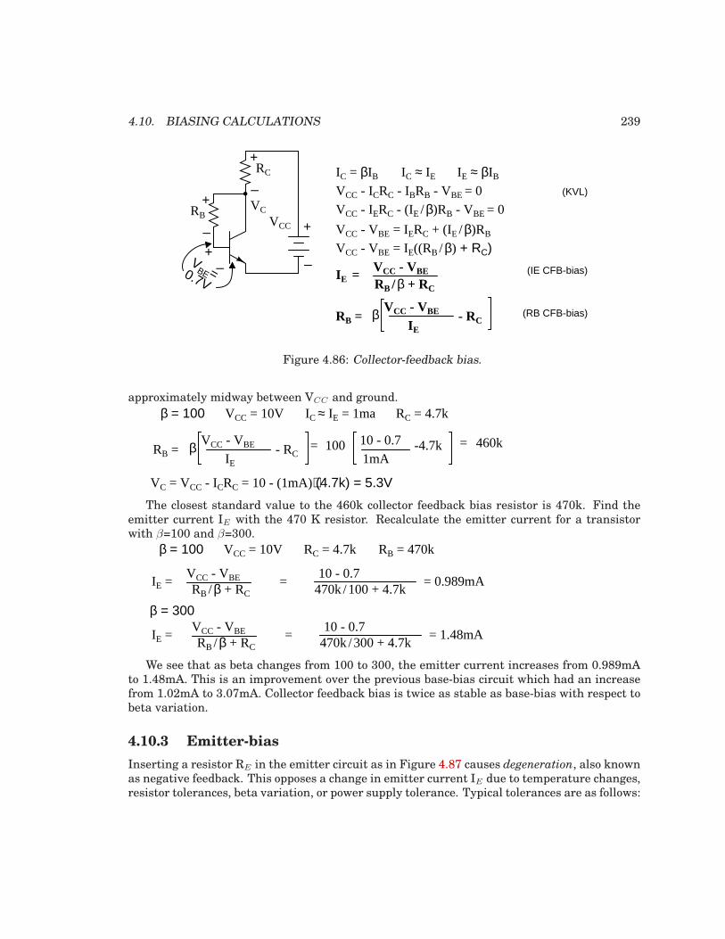
4.10. BIASING CALCULATIONS 239
VBE=0.7V
+
_
RC
RBVCC
+
_
+_
VCC - VBE = IE((RB /β) + RC)VCC - VBE
RB /β + RCIE =
IC = βIB
VCC - VBE = IERC + (IE /β)RB
VCC - VBE
IE - RCRB = β
+
_IC ≈ IE IE ≈ βIB
VCC - IERC - (IE /β)RB - VBE = 0
VCC - ICRC - IBRB - VBE = 0
(IE CFB-bias)
(RB CFB-bias)
(KVL)
VC
Figure 4.86: Collector-feedback bias.
approximately midway between VCC and ground.
β = 100 IC ≈ IE = 1maVCC = 10V RC = 4.7k
10 - 0.7=1mA
= 460kVCC - VBE
IE - RCRB = β 100 -4.7k
VC = VCC - ICRC = 10 - (1mA)⋅(4.7k) = 5.3V
The closest standard value to the 460k collector feedback bias resistor is 470k. Find theemitter current IE with the 470 K resistor. Recalculate the emitter current for a transistorwith β=100 and β=300.
VCC - VBE
RB /β + RCIE =
10 - 0.7470k /100 + 4.7k
= = 0.989mA
β = 100 VCC = 10V RC = 4.7k RB = 470k
VCC - VBE
RB /β + RCIE =
10 - 0.7470k /300 + 4.7k
= = 1.48mA
β = 300
We see that as beta changes from 100 to 300, the emitter current increases from 0.989mAto 1.48mA. This is an improvement over the previous base-bias circuit which had an increasefrom 1.02mA to 3.07mA. Collector feedback bias is twice as stable as base-bias with respect tobeta variation.
4.10.3 Emitter-bias
Inserting a resistor RE in the emitter circuit as in Figure 4.87 causes degeneration, also knownas negative feedback. This opposes a change in emitter current IE due to temperature changes,resistor tolerances, beta variation, or power supply tolerance. Typical tolerances are as follows:
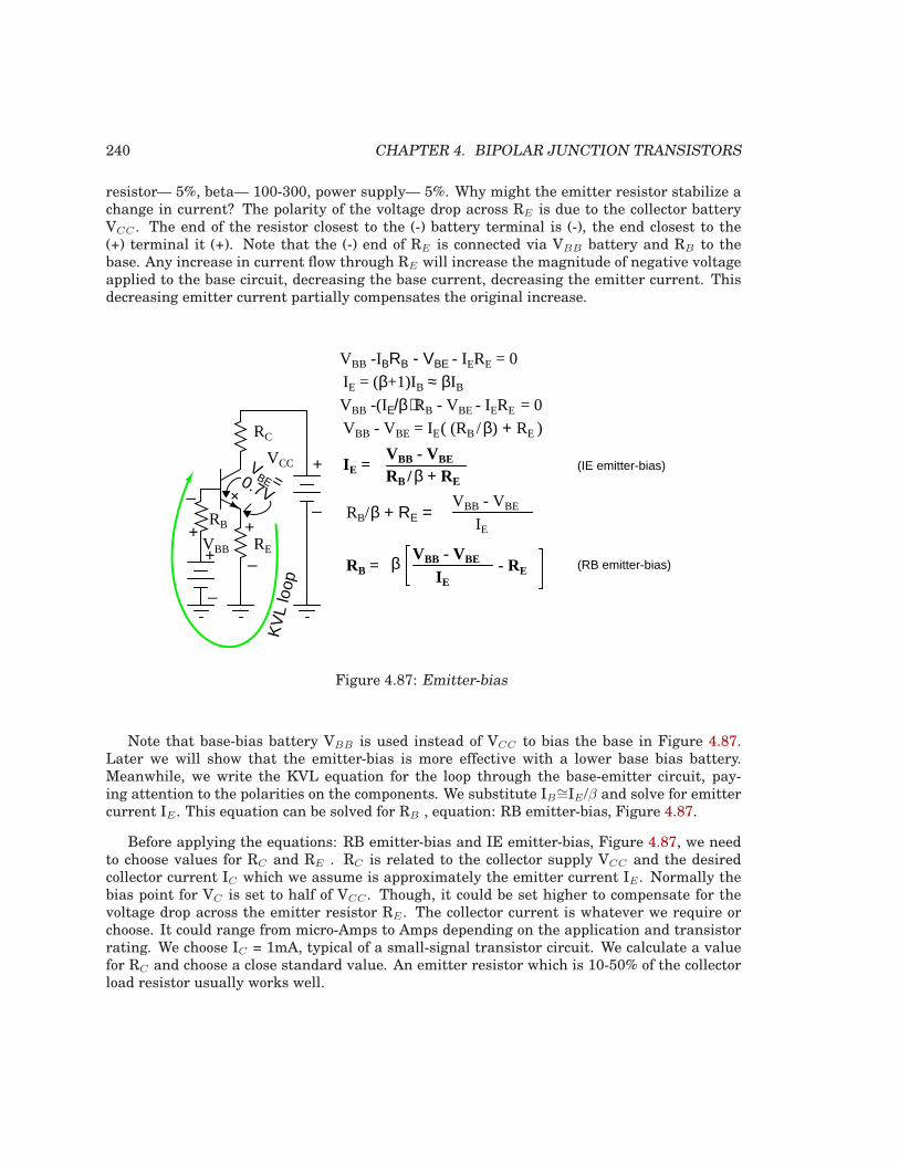
240 CHAPTER 4. BIPOLAR JUNCTION TRANSISTORS
resistor— 5%, beta— 100-300, power supply— 5%. Why might the emitter resistor stabilize achange in current? The polarity of the voltage drop across RE is due to the collector batteryVCC . The end of the resistor closest to the (-) battery terminal is (-), the end closest to the(+) terminal it (+). Note that the (-) end of RE is connected via VBB battery and RB to thebase. Any increase in current flow through RE will increase the magnitude of negative voltageapplied to the base circuit, decreasing the base current, decreasing the emitter current. Thisdecreasing emitter current partially compensates the original increase.
VBE=0.7V
+
_
RC
RB
VCC
+
_
VBB -IΒRB - VBE - IERE = 0
VBB - VBE = IE( (RB /β) + RE )
VBB - VBE
RB /β + REIE =
IE = (β+1)IB ≈ βIB
VBB -(IΕ/β)RB - VBE - IERE = 0
_
+
VBB - VBERB/β + RE = IE
VBB - VBE
IE - RE RB = β
RE
(IE emitter-bias)
(RB emitter-bias)
VBB+
_
+
KV
L lo
op
_
Figure 4.87: Emitter-bias
Note that base-bias battery VBB is used instead of VCC to bias the base in Figure 4.87.Later we will show that the emitter-bias is more effective with a lower base bias battery.Meanwhile, we write the KVL equation for the loop through the base-emitter circuit, pay-ing attention to the polarities on the components. We substitute IB∼=IE /β and solve for emittercurrent IE . This equation can be solved for RB , equation: RB emitter-bias, Figure 4.87.
Before applying the equations: RB emitter-bias and IE emitter-bias, Figure 4.87, we needto choose values for RC and RE . RC is related to the collector supply VCC and the desiredcollector current IC which we assume is approximately the emitter current IE . Normally thebias point for VC is set to half of VCC . Though, it could be set higher to compensate for thevoltage drop across the emitter resistor RE . The collector current is whatever we require orchoose. It could range from micro-Amps to Amps depending on the application and transistorrating. We choose IC = 1mA, typical of a small-signal transistor circuit. We calculate a valuefor RC and choose a close standard value. An emitter resistor which is 10-50% of the collectorload resistor usually works well.
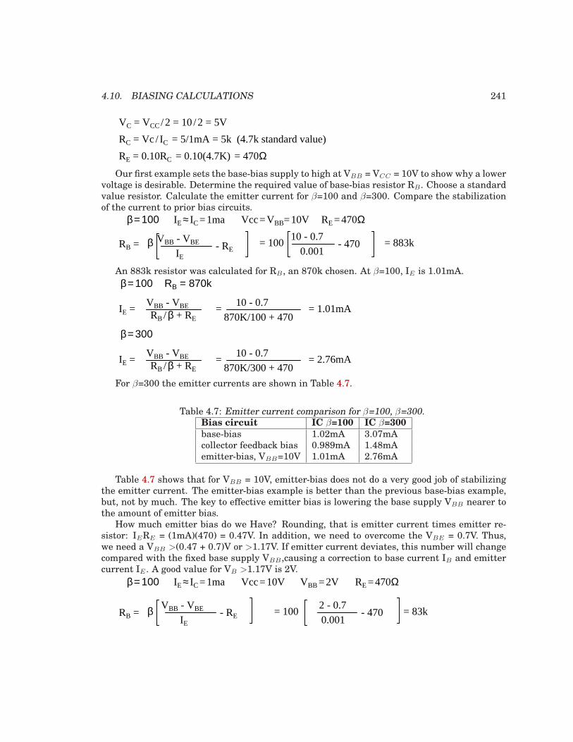
4.10. BIASING CALCULATIONS 241
VC = VCC / 2 = 10 /2 = 5V
RC = Vc / IC = 5/1mA = 5k (4.7k standard value)
RE = 0.10RC = 0.10(4.7K) = 470Ω
Our first example sets the base-bias supply to high at VBB = VCC = 10V to show why a lowervoltage is desirable. Determine the required value of base-bias resistor RB . Choose a standardvalue resistor. Calculate the emitter current for β=100 and β=300. Compare the stabilizationof the current to prior bias circuits.
β=100 IE ≈ IC =1ma Vcc=VBB=10V
10 - 0.7
0.001- 470= 100 = 883k
RE = 470Ω
VBB - VBE
IE - RE
RB = β
An 883k resistor was calculated for RB , an 870k chosen. At β=100, IE is 1.01mA.
β=100 RB = 870k
VBB - VBE
RB /β + RE IE = = 1.01mA
10 - 0.7
870K/100 + 470=
β=300
VBB - VBE
RB /β + RE IE = = 2.76mA
10 - 0.7
870K/300 + 470=
For β=300 the emitter currents are shown in Table 4.7.
Table 4.7: Emitter current comparison for β=100, β=300.Bias circuit IC β=100 IC β=300
base-bias 1.02mA 3.07mAcollector feedback bias 0.989mA 1.48mAemitter-bias, VBB=10V 1.01mA 2.76mA
Table 4.7 shows that for VBB = 10V, emitter-bias does not do a very good job of stabilizingthe emitter current. The emitter-bias example is better than the previous base-bias example,but, not by much. The key to effective emitter bias is lowering the base supply VBB nearer tothe amount of emitter bias.
How much emitter bias do we Have? Rounding, that is emitter current times emitter re-sistor: IERE = (1mA)(470) = 0.47V. In addition, we need to overcome the VBE = 0.7V. Thus,we need a VBB >(0.47 + 0.7)V or >1.17V. If emitter current deviates, this number will changecompared with the fixed base supply VBB ,causing a correction to base current IB and emittercurrent IE . A good value for VB >1.17V is 2V.
2 - 0.7
0.001- 470= 100 = 83k
VBB - VBE
IE - RE RB = β
β=100 IE ≈ IC =1ma Vcc=10V RE = 470ΩVBB =2V
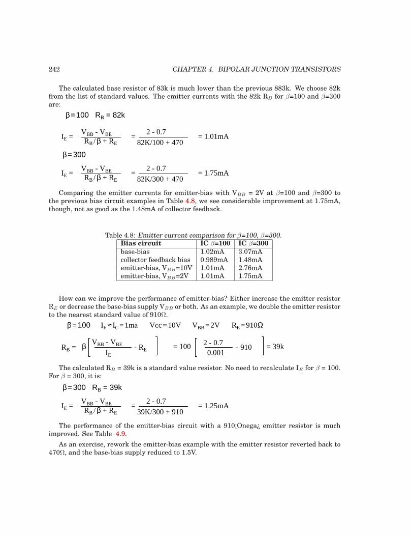
242 CHAPTER 4. BIPOLAR JUNCTION TRANSISTORS
The calculated base resistor of 83k is much lower than the previous 883k. We choose 82kfrom the list of standard values. The emitter currents with the 82k RB for β=100 and β=300are:
VBB - VBE
RB /β + RE IE =
β=100 RB = 82k
= 1.01mA 2 - 0.7
82K/100 + 470=
VBB - VBE
RB /β + RE IE =
β=300
= 1.75mA 2 - 0.7
82K/300 + 470=
Comparing the emitter currents for emitter-bias with VBB = 2V at β=100 and β=300 tothe previous bias circuit examples in Table 4.8, we see considerable improvement at 1.75mA,though, not as good as the 1.48mA of collector feedback.
Table 4.8: Emitter current comparison for β=100, β=300.Bias circuit IC β=100 IC β=300
base-bias 1.02mA 3.07mAcollector feedback bias 0.989mA 1.48mAemitter-bias, VBB=10V 1.01mA 2.76mAemitter-bias, VBB=2V 1.01mA 1.75mA
How can we improve the performance of emitter-bias? Either increase the emitter resistorRE or decrease the base-bias supply VBB or both. As an example, we double the emitter resistorto the nearest standard value of 910Ω.
2 - 0.70.001
- 910= 100 = 39kVBB - VBE
IE - RE RB = β
β=100 IE ≈ IC =1ma Vcc=10V RE = 910ΩVBB =2V
The calculated RB = 39k is a standard value resistor. No need to recalculate IE for β = 100.For β = 300, it is:
β=300 RB = 39k
VBB - VBE
RB /β + RE IE = = 1.25mA
2 - 0.7
39K/300 + 910=
The performance of the emitter-bias circuit with a 910¡Onega¿ emitter resistor is muchimproved. See Table 4.9.
As an exercise, rework the emitter-bias example with the emitter resistor reverted back to470Ω, and the base-bias supply reduced to 1.5V.
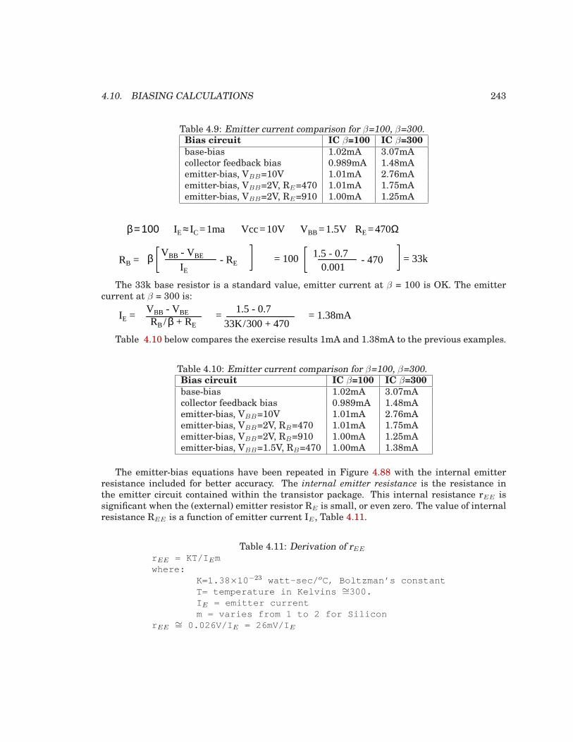
4.10. BIASING CALCULATIONS 243
Table 4.9: Emitter current comparison for β=100, β=300.Bias circuit IC β=100 IC β=300
base-bias 1.02mA 3.07mAcollector feedback bias 0.989mA 1.48mAemitter-bias, VBB=10V 1.01mA 2.76mAemitter-bias, VBB=2V, RE=470 1.01mA 1.75mAemitter-bias, VBB=2V, RE=910 1.00mA 1.25mA
1.5 - 0.70.001
- 470= 100 = 33kVBB - VBE
IE - RE RB = β
β=100 IE ≈ IC =1ma Vcc=10V RE = 470ΩVBB =1.5V
The 33k base resistor is a standard value, emitter current at β = 100 is OK. The emittercurrent at β = 300 is:
VBB - VBE
RB /β + RE IE = = 1.38mA
1.5 - 0.7
33K/300 + 470=
Table 4.10 below compares the exercise results 1mA and 1.38mA to the previous examples.
Table 4.10: Emitter current comparison for β=100, β=300.Bias circuit IC β=100 IC β=300
base-bias 1.02mA 3.07mAcollector feedback bias 0.989mA 1.48mAemitter-bias, VBB=10V 1.01mA 2.76mAemitter-bias, VBB=2V, RB=470 1.01mA 1.75mAemitter-bias, VBB=2V, RB=910 1.00mA 1.25mAemitter-bias, VBB=1.5V, RB=470 1.00mA 1.38mA
The emitter-bias equations have been repeated in Figure 4.88 with the internal emitterresistance included for better accuracy. The internal emitter resistance is the resistance inthe emitter circuit contained within the transistor package. This internal resistance rEE issignificant when the (external) emitter resistor RE is small, or even zero. The value of internalresistance REE is a function of emitter current IE , Table 4.11.
Table 4.11: Derivation of rEE
r EE = KT/I Emwhere:
K=1.38 ×10⁻²³ watt-sec/ oC, Boltzman’s constantT= temperature in Kelvins ∼=300.I E = emitter currentm = varies from 1 to 2 for Silicon
r EE∼= 0.026V/I E = 26mV/I E
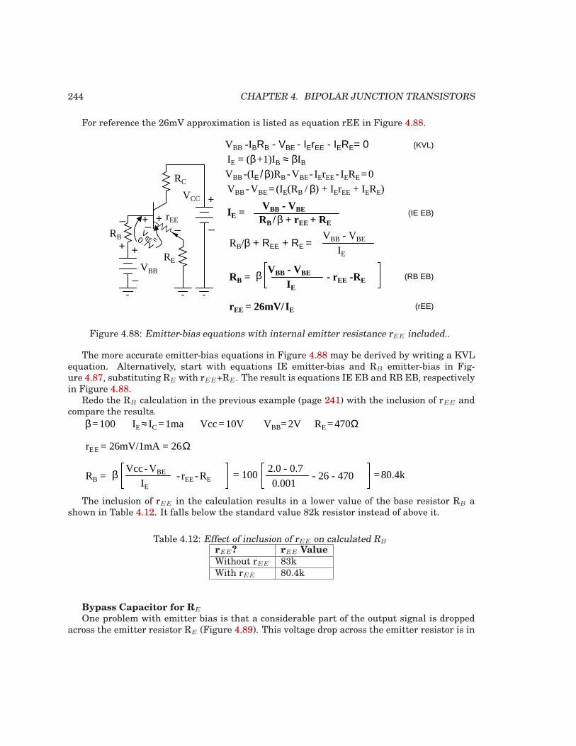
244 CHAPTER 4. BIPOLAR JUNCTION TRANSISTORS
For reference the 26mV approximation is listed as equation rEE in Figure 4.88.
+
_
RC
RB
VCC
_ _ rEE_
+
RE
VBB -IΒRB - VBE - IErEE - IERE= 0
VBB -VBE =(IE(RB / β) + IErEE + IERE)
VBB - VBE
RB /β + rEE + REIE =
IE = (β+1)IB ≈ βIB
VBB -(IE /β)RB -VBE- IErEE - IERE =0
VBB - VBERB/β + REE + RE = IE
VBB - VBE
IE - rEE -RERB = β
+
_VBB
+V
BE=0.7V
+
rEE = 26mV/IE (rEE)
(IE EB)
(RB EB)
(KVL)
Figure 4.88: Emitter-bias equations with internal emitter resistance rEE included..
The more accurate emitter-bias equations in Figure 4.88 may be derived by writing a KVLequation. Alternatively, start with equations IE emitter-bias and RB emitter-bias in Fig-ure 4.87, substituting RE with rEE+RE . The result is equations IE EB and RB EB, respectivelyin Figure 4.88.
Redo the RB calculation in the previous example (page 241) with the inclusion of rEE andcompare the results.
β=100 IE ≈ IC =1ma Vcc=10V
2.0 - 0.7
0.001- 26 - 470= 100
rE E = 26mV/1mA = 26Ω
=80.4k
RE = 470Ω
Vcc-VBE
IE - rEE -RERB = β
VBB=2V
The inclusion of rEE in the calculation results in a lower value of the base resistor RB ashown in Table 4.12. It falls below the standard value 82k resistor instead of above it.
Table 4.12: Effect of inclusion of rEE on calculated RB
rEE? rEE Value
Without rEE 83kWith rEE 80.4k
Bypass Capacitor for RE
One problem with emitter bias is that a considerable part of the output signal is droppedacross the emitter resistor RE (Figure 4.89). This voltage drop across the emitter resistor is in
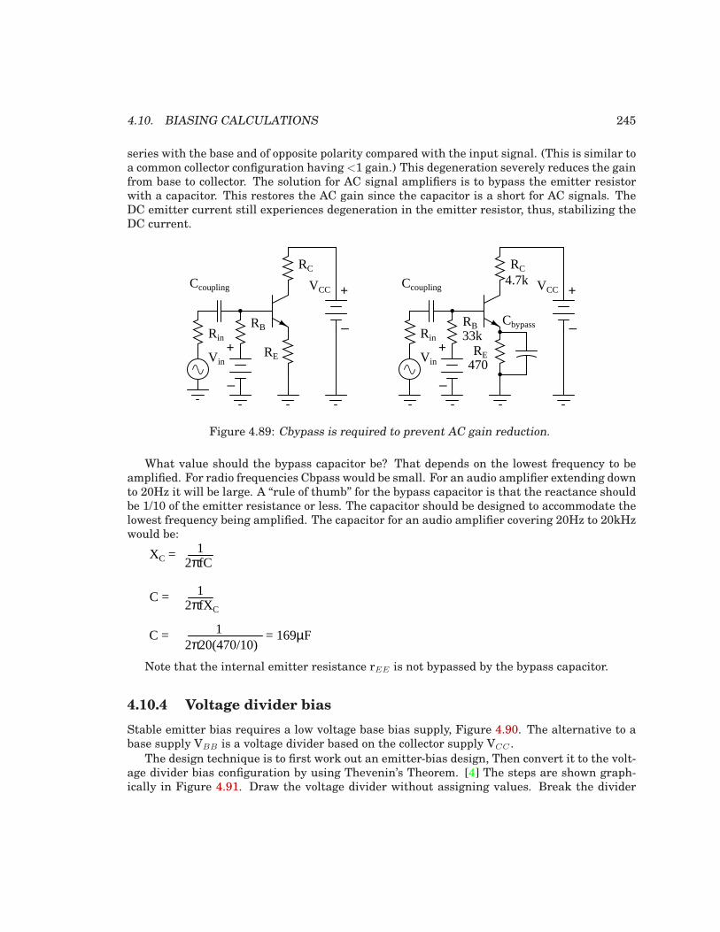
4.10. BIASING CALCULATIONS 245
series with the base and of opposite polarity compared with the input signal. (This is similar toa common collector configuration having <1 gain.) This degeneration severely reduces the gainfrom base to collector. The solution for AC signal amplifiers is to bypass the emitter resistorwith a capacitor. This restores the AC gain since the capacitor is a short for AC signals. TheDC emitter current still experiences degeneration in the emitter resistor, thus, stabilizing theDC current.
+
_
RC
VCC
RE
+
_
RC
VCC
RE
CbypassRin
Vin
Ccoupling
Rin
Vin
Ccoupling4.7k
470
RB RB33k
+
_
+
_
Figure 4.89: Cbypass is required to prevent AC gain reduction.
What value should the bypass capacitor be? That depends on the lowest frequency to beamplified. For radio frequencies Cbpass would be small. For an audio amplifier extending downto 20Hz it will be large. A “rule of thumb” for the bypass capacitor is that the reactance shouldbe 1/10 of the emitter resistance or less. The capacitor should be designed to accommodate thelowest frequency being amplified. The capacitor for an audio amplifier covering 20Hz to 20kHzwould be:
XC = 2πfC
1
C = 2πfXC
1
C = 2π20(470/10)
1 = 169µF
Note that the internal emitter resistance rEE is not bypassed by the bypass capacitor.
4.10.4 Voltage divider bias
Stable emitter bias requires a low voltage base bias supply, Figure 4.90. The alternative to abase supply VBB is a voltage divider based on the collector supply VCC .
The design technique is to first work out an emitter-bias design, Then convert it to the volt-age divider bias configuration by using Thevenin’s Theorem. [4] The steps are shown graph-ically in Figure 4.91. Draw the voltage divider without assigning values. Break the divider
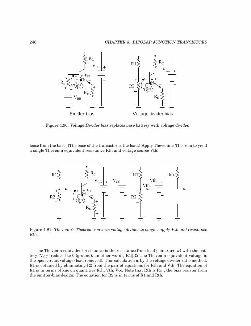
246 CHAPTER 4. BIPOLAR JUNCTION TRANSISTORS
+
_
RC
RB
VCC
_ _ rEE_
+
RE+
_VBB
+V
BE=0.7V
++
_
RC
VCC
_
_ rEE_
+
RE
+V
BE=0.7V
+
R1
R2+
_+
_
Emitter-bias Voltage divider bias
Figure 4.90: Voltage Divider bias replaces base battery with voltage divider.
loose from the base. (The base of the transistor is the load.) Apply Thevenin’s Theorem to yielda single Thevenin equivalent resistance Rth and voltage source Vth.
+
_
RC
VCC
_ rEE_
+
RE
VBE=0.7V
++
R1
R2_
+
R1
R2
+
_
VCC
Rth
+
_
Vth
_
+
Vth
-
Figure 4.91: Thevenin’s Theorem converts voltage divider to single supply Vth and resistanceRth.
The Thevenin equivalent resistance is the resistance from load point (arrow) with the bat-tery (VCC ) reduced to 0 (ground). In other words, R1||R2.The Thevenin equivalent voltage isthe open circuit voltage (load removed). This calculation is by the voltage divider ratio method.R1 is obtained by eliminating R2 from the pair of equations for Rth and Vth. The equation ofR1 is in terms of known quantities Rth, Vth, Vcc. Note that Rth is RB , the bias resistor fromthe emitter-bias design. The equation for R2 is in terms of R1 and Rth.
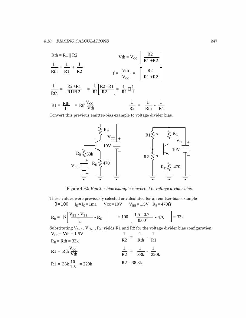
4.10. BIASING CALCULATIONS 247
Rth = R1 || R2 Vth = VCCR2
R1 +R2
Rth
1 1 1
R1 R2+=
Vth R2
R1 +R2VCC
=f =
R1⋅R2R2+R1
Rth
1= =
R2+R1R11
R2=
R11
f1⋅
R1 = f
RthVth
VCC=Rth
1 11
R1R2-=Rth
Convert this previous emitter-bias example to voltage divider bias.
+
_
RC
RB
VCC
RE
_VBB
+
+
_
RC
VCC
RE
R1
R2
470
33k
470
?
?
10V10V
Figure 4.92: Emitter-bias example converted to voltage divider bias.
These values were previously selected or calculated for an emitter-bias example
1.5 - 0.70.001
- 470= 100 = 33kVBB - VBE
IE - RE RB = β
β=100 IE ≈ IC =1ma Vcc=10V RE = 470ΩVBB =1.5V
Substituting VCC , VBB , RB yields R1 and R2 for the voltage divider bias configuration.
R1 Vth
VCC= Rth
Rth
1 11
R1R2-=
RB = Rth = 33k
VBB = Vth = 1.5V
R1 1.510= 33k = 220k
33k
1 11
220kR2-=
R2 = 38.8k
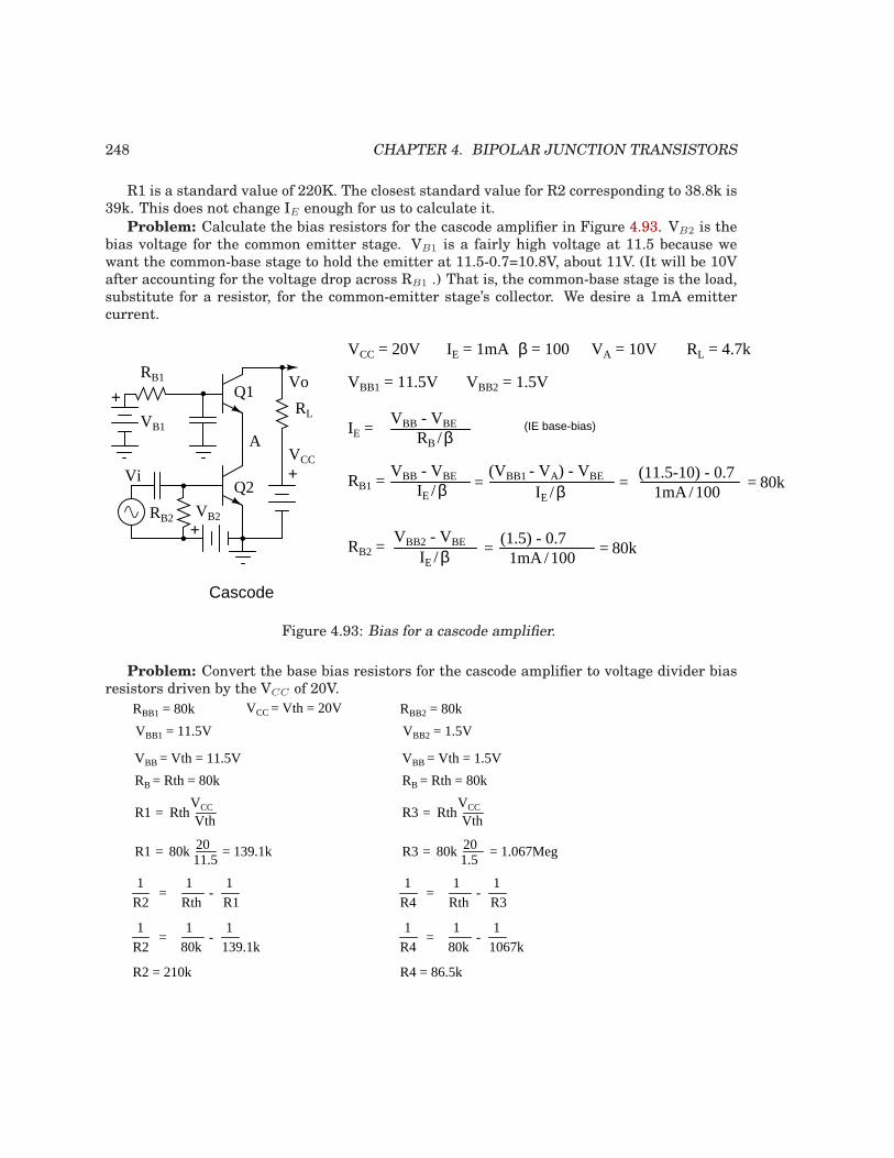
248 CHAPTER 4. BIPOLAR JUNCTION TRANSISTORS
R1 is a standard value of 220K. The closest standard value for R2 corresponding to 38.8k is39k. This does not change IE enough for us to calculate it.
Problem: Calculate the bias resistors for the cascode amplifier in Figure 4.93. VB2 is thebias voltage for the common emitter stage. VB1 is a fairly high voltage at 11.5 because wewant the common-base stage to hold the emitter at 11.5-0.7=10.8V, about 11V. (It will be 10Vafter accounting for the voltage drop across RB1 .) That is, the common-base stage is the load,substitute for a resistor, for the common-emitter stage’s collector. We desire a 1mA emittercurrent.
RL
Vi
Vo
Cascode
+
+
+
AVCC
Q1
Q2
RB1
RB2
VB1
VB2
VBB - VBE
RB /βIE = (IE base-bias)
VBB - VBE
IE /βRB1 =(11.5-10) - 0.7
1mA/100= = 80k
VCC = 20V IE = 1mA β = 100 VA = 10V
VBB2 - VBE
IE /βRB2 =(1.5) - 0.7
1mA/100= = 80k
VBB2 = 1.5VVBB1 = 11.5V
(VBB1 - VA) - VBE
IE /β=
RL = 4.7k
Figure 4.93: Bias for a cascode amplifier.
Problem: Convert the base bias resistors for the cascode amplifier to voltage divider biasresistors driven by the VCC of 20V.
R1 Vth
VCC= Rth
RB = Rth = 80k
VBB = Vth = 11.5V
R1 11.520= 80k = 139.1k
R3 Vth
VCC= Rth
RB = Rth = 80k
VBB = Vth = 1.5V
R3 1.520= 80k = 1.067Meg
VBB2 = 1.5VVBB1 = 11.5V
RBB2 = 80kRBB1 = 80k VCC = Vth = 20V
Rth
1 11
R1R2-=
80k
1 11
139.1kR2-=
R2 = 210k
Rth
1 11
R3R4-=
80k
1 11
1067kR4-=
R4 = 86.5k
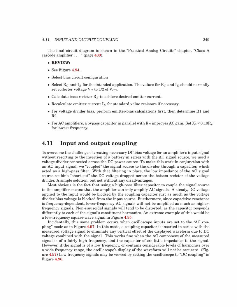
4.11. INPUT AND OUTPUT COUPLING 249
The final circuit diagram is shown in the “Practical Analog Circuits” chapter, “Class Acascode amplifier . . . ” (page 433).
• REVIEW:
• See Figure 4.94.
• Select bias circuit configuration
• Select RC and IE for the intended application. The values for RC and IE should normallyset collector voltage VC to 1/2 of VCC .
• Calculate base resistor RB to achieve desired emitter current.
• Recalculate emitter current IE for standard value resistors if necessary.
• For voltage divider bias, perform emitter-bias calculations first, then determine R1 andR2.
• For AC amplifiers, a bypass capacitor in parallel with RE improves AC gain. Set XC≤0.10RE
for lowest frequency.
4.11 Input and output coupling
To overcome the challenge of creating necessary DC bias voltage for an amplifier’s input signalwithout resorting to the insertion of a battery in series with the AC signal source, we used avoltage divider connected across the DC power source. To make this work in conjunction withan AC input signal, we “coupled” the signal source to the divider through a capacitor, whichacted as a high-pass filter. With that filtering in place, the low impedance of the AC signalsource couldn’t “short out” the DC voltage dropped across the bottom resistor of the voltagedivider. A simple solution, but not without any disadvantages.
Most obvious is the fact that using a high-pass filter capacitor to couple the signal sourceto the amplifier means that the amplifier can only amplify AC signals. A steady, DC voltageapplied to the input would be blocked by the coupling capacitor just as much as the voltagedivider bias voltage is blocked from the input source. Furthermore, since capacitive reactanceis frequency-dependent, lower-frequency AC signals will not be amplified as much as higher-frequency signals. Non-sinusoidal signals will tend to be distorted, as the capacitor respondsdifferently to each of the signal’s constituent harmonics. An extreme example of this would bea low-frequency square-wave signal in Figure 4.95.
Incidentally, this same problem occurs when oscilloscope inputs are set to the “AC cou-pling” mode as in Figure 4.97. In this mode, a coupling capacitor is inserted in series with themeasured voltage signal to eliminate any vertical offset of the displayed waveform due to DCvoltage combined with the signal. This works fine when the AC component of the measuredsignal is of a fairly high frequency, and the capacitor offers little impedance to the signal.However, if the signal is of a low frequency, or contains considerable levels of harmonics overa wide frequency range, the oscilloscope’s display of the waveform will not be accurate. (Fig-ure 4.97) Low frequency signals may be viewed by setting the oscilloscope to “DC coupling” inFigure 4.96.
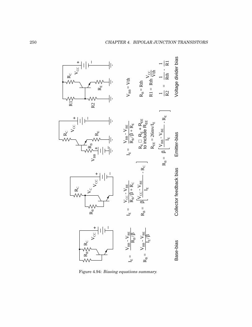
250 CHAPTER 4. BIPOLAR JUNCTION TRANSISTORS
+ _
RC
RB
VC
C
VB
B -
VB
E
RB
/βI E
=
+ _
RC
RB
VC
C
VC
C -
VB
E
RB
/β +
RC
I E =
VC
C -
VB
E
I E
- R
CR
B =
β
VC
+ _
RC
RB
VC
C
VB
B -
VB
E
RB
/β +
RE
I E =
VB
B -
VB
E
I E
- R
E
RB =
β
RE
VB
B+ _
+ _
RC V
CC
RE
R1
Vol
tage
div
ider
bia
s
RB
= R
th
VB
B =
Vth
R1
=
Vth
VC
C
Rth
11
1
R1
R2
-=R
th
VB
B -
VB
E
I E/β
RB =
Em
itter
-bia
sC
olle
ctor
feed
back
bia
sB
ase-
bias
RE ⇐
RE +
RE
E
to in
clud
e R
EE
RE
E =
26m
v/I E
R2
Figure 4.94: Biasing equations summary.
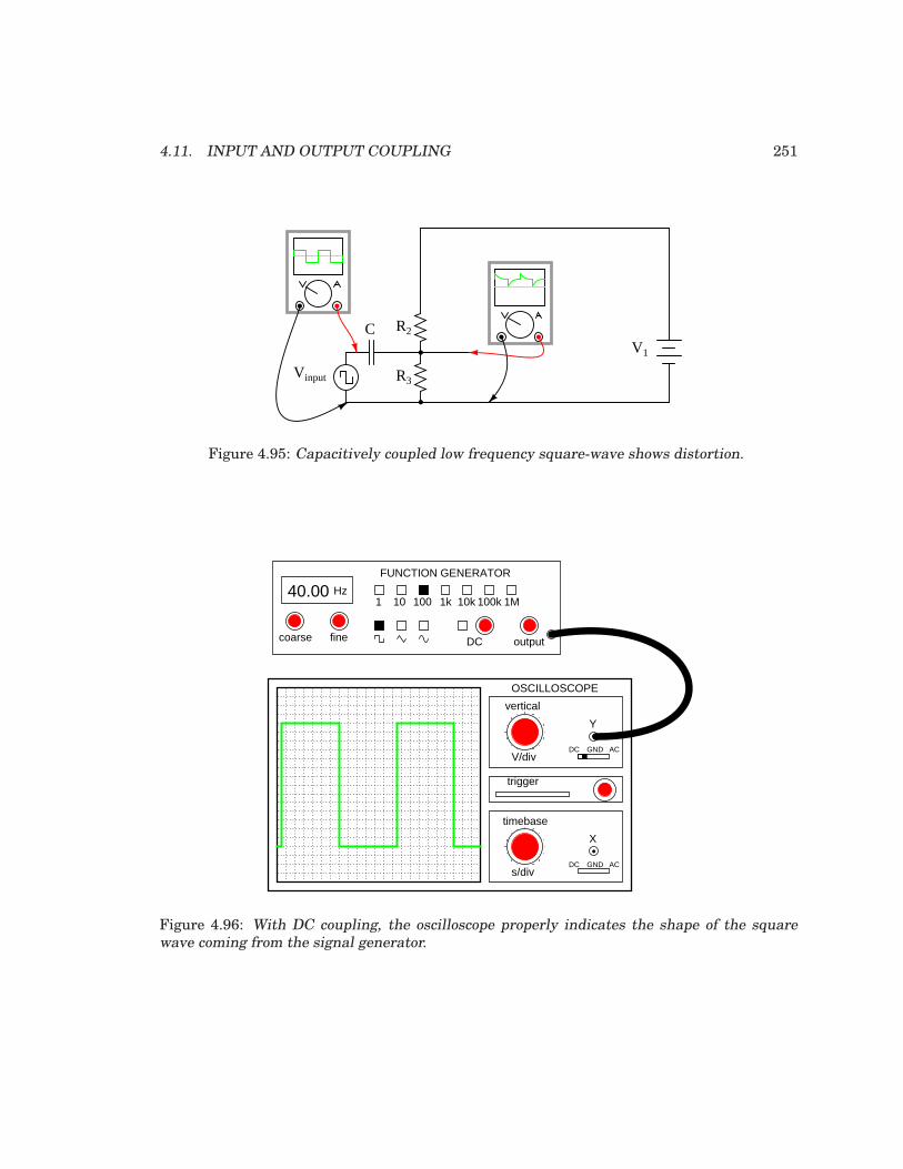
4.11. INPUT AND OUTPUT COUPLING 251
V1
Vinput
R2
R3
C
Figure 4.95: Capacitively coupled low frequency square-wave shows distortion.
trigger
timebase
s/divDC GND AC
X
GNDDCV/div
vertical
OSCILLOSCOPE
Y
AC
Hz
FUNCTION GENERATOR
1 10 100 1k 10k 100k 1M
outputDCfinecoarse
40.00
Figure 4.96: With DC coupling, the oscilloscope properly indicates the shape of the squarewave coming from the signal generator.
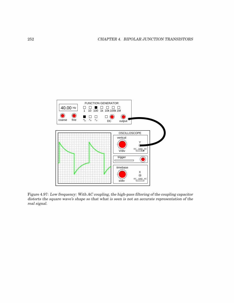
252 CHAPTER 4. BIPOLAR JUNCTION TRANSISTORS
trigger
timebase
s/divDC GND AC
X
GNDDCV/div
vertical
OSCILLOSCOPE
Y
AC
Hz
FUNCTION GENERATOR
1 10 100 1k 10k 100k 1M
outputDCfinecoarse
40.00
Figure 4.97: Low frequency: With AC coupling, the high-pass filtering of the coupling capacitordistorts the square wave’s shape so that what is seen is not an accurate representation of thereal signal.
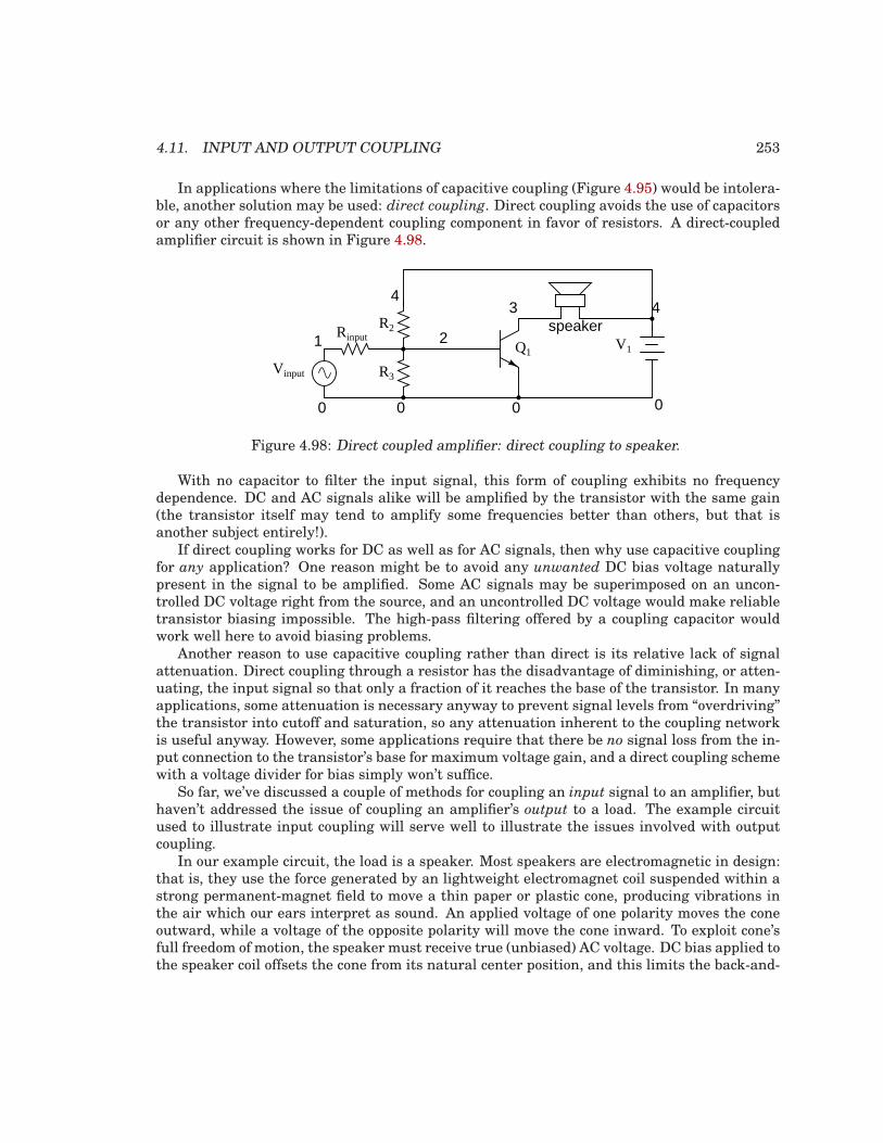
4.11. INPUT AND OUTPUT COUPLING 253
In applications where the limitations of capacitive coupling (Figure 4.95) would be intolera-ble, another solution may be used: direct coupling. Direct coupling avoids the use of capacitorsor any other frequency-dependent coupling component in favor of resistors. A direct-coupledamplifier circuit is shown in Figure 4.98.
speakerV1Q1
1
0 0
2
3 4
Vinput
4
0
R2
R3
0
Rinput
Figure 4.98: Direct coupled amplifier: direct coupling to speaker.
With no capacitor to filter the input signal, this form of coupling exhibits no frequencydependence. DC and AC signals alike will be amplified by the transistor with the same gain(the transistor itself may tend to amplify some frequencies better than others, but that isanother subject entirely!).
If direct coupling works for DC as well as for AC signals, then why use capacitive couplingfor any application? One reason might be to avoid any unwanted DC bias voltage naturallypresent in the signal to be amplified. Some AC signals may be superimposed on an uncon-trolled DC voltage right from the source, and an uncontrolled DC voltage would make reliabletransistor biasing impossible. The high-pass filtering offered by a coupling capacitor wouldwork well here to avoid biasing problems.
Another reason to use capacitive coupling rather than direct is its relative lack of signalattenuation. Direct coupling through a resistor has the disadvantage of diminishing, or atten-uating, the input signal so that only a fraction of it reaches the base of the transistor. In manyapplications, some attenuation is necessary anyway to prevent signal levels from “overdriving”the transistor into cutoff and saturation, so any attenuation inherent to the coupling networkis useful anyway. However, some applications require that there be no signal loss from the in-put connection to the transistor’s base for maximum voltage gain, and a direct coupling schemewith a voltage divider for bias simply won’t suffice.
So far, we’ve discussed a couple of methods for coupling an input signal to an amplifier, buthaven’t addressed the issue of coupling an amplifier’s output to a load. The example circuitused to illustrate input coupling will serve well to illustrate the issues involved with outputcoupling.
In our example circuit, the load is a speaker. Most speakers are electromagnetic in design:that is, they use the force generated by an lightweight electromagnet coil suspended within astrong permanent-magnet field to move a thin paper or plastic cone, producing vibrations inthe air which our ears interpret as sound. An applied voltage of one polarity moves the coneoutward, while a voltage of the opposite polarity will move the cone inward. To exploit cone’sfull freedom of motion, the speaker must receive true (unbiased) AC voltage. DC bias applied tothe speaker coil offsets the cone from its natural center position, and this limits the back-and-
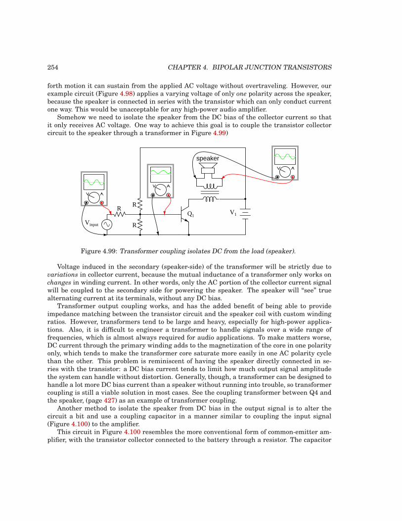
254 CHAPTER 4. BIPOLAR JUNCTION TRANSISTORS
forth motion it can sustain from the applied AC voltage without overtraveling. However, ourexample circuit (Figure 4.98) applies a varying voltage of only one polarity across the speaker,because the speaker is connected in series with the transistor which can only conduct currentone way. This would be unacceptable for any high-power audio amplifier.
Somehow we need to isolate the speaker from the DC bias of the collector current so thatit only receives AC voltage. One way to achieve this goal is to couple the transistor collectorcircuit to the speaker through a transformer in Figure 4.99)
speaker
V1Q1
Vinput
RR
R
Figure 4.99: Transformer coupling isolates DC from the load (speaker).
Voltage induced in the secondary (speaker-side) of the transformer will be strictly due tovariations in collector current, because the mutual inductance of a transformer only works onchanges in winding current. In other words, only the AC portion of the collector current signalwill be coupled to the secondary side for powering the speaker. The speaker will “see” truealternating current at its terminals, without any DC bias.
Transformer output coupling works, and has the added benefit of being able to provideimpedance matching between the transistor circuit and the speaker coil with custom windingratios. However, transformers tend to be large and heavy, especially for high-power applica-tions. Also, it is difficult to engineer a transformer to handle signals over a wide range offrequencies, which is almost always required for audio applications. To make matters worse,DC current through the primary winding adds to the magnetization of the core in one polarityonly, which tends to make the transformer core saturate more easily in one AC polarity cyclethan the other. This problem is reminiscent of having the speaker directly connected in se-ries with the transistor: a DC bias current tends to limit how much output signal amplitudethe system can handle without distortion. Generally, though, a transformer can be designed tohandle a lot more DC bias current than a speaker without running into trouble, so transformercoupling is still a viable solution in most cases. See the coupling transformer between Q4 andthe speaker, (page 427) as an example of transformer coupling.
Another method to isolate the speaker from DC bias in the output signal is to alter thecircuit a bit and use a coupling capacitor in a manner similar to coupling the input signal(Figure 4.100) to the amplifier.
This circuit in Figure 4.100 resembles the more conventional form of common-emitter am-plifier, with the transistor collector connected to the battery through a resistor. The capacitor
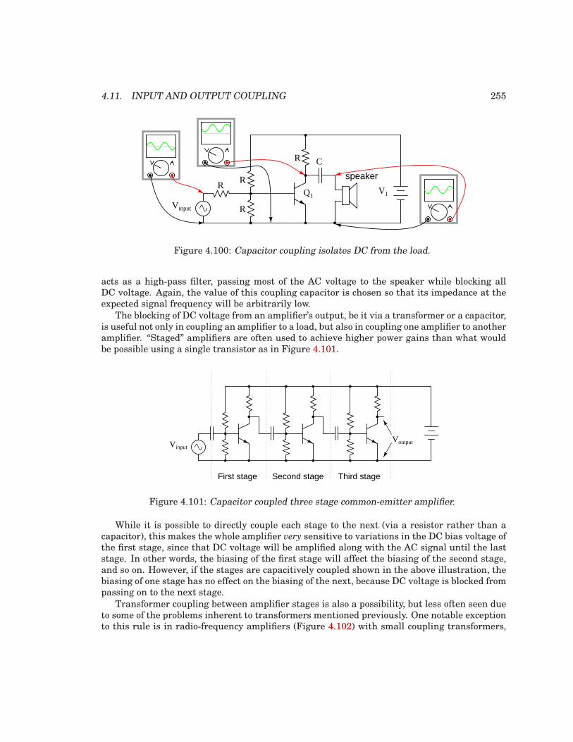
4.11. INPUT AND OUTPUT COUPLING 255
speaker
V1Q1
Vinput
CR
R
R
R
Figure 4.100: Capacitor coupling isolates DC from the load.
acts as a high-pass filter, passing most of the AC voltage to the speaker while blocking allDC voltage. Again, the value of this coupling capacitor is chosen so that its impedance at theexpected signal frequency will be arbitrarily low.
The blocking of DC voltage from an amplifier’s output, be it via a transformer or a capacitor,is useful not only in coupling an amplifier to a load, but also in coupling one amplifier to anotheramplifier. “Staged” amplifiers are often used to achieve higher power gains than what wouldbe possible using a single transistor as in Figure 4.101.
VinputVoutput
First stage Second stage Third stage
Figure 4.101: Capacitor coupled three stage common-emitter amplifier.
While it is possible to directly couple each stage to the next (via a resistor rather than acapacitor), this makes the whole amplifier very sensitive to variations in the DC bias voltage ofthe first stage, since that DC voltage will be amplified along with the AC signal until the laststage. In other words, the biasing of the first stage will affect the biasing of the second stage,and so on. However, if the stages are capacitively coupled shown in the above illustration, thebiasing of one stage has no effect on the biasing of the next, because DC voltage is blocked frompassing on to the next stage.
Transformer coupling between amplifier stages is also a possibility, but less often seen dueto some of the problems inherent to transformers mentioned previously. One notable exceptionto this rule is in radio-frequency amplifiers (Figure 4.102) with small coupling transformers,
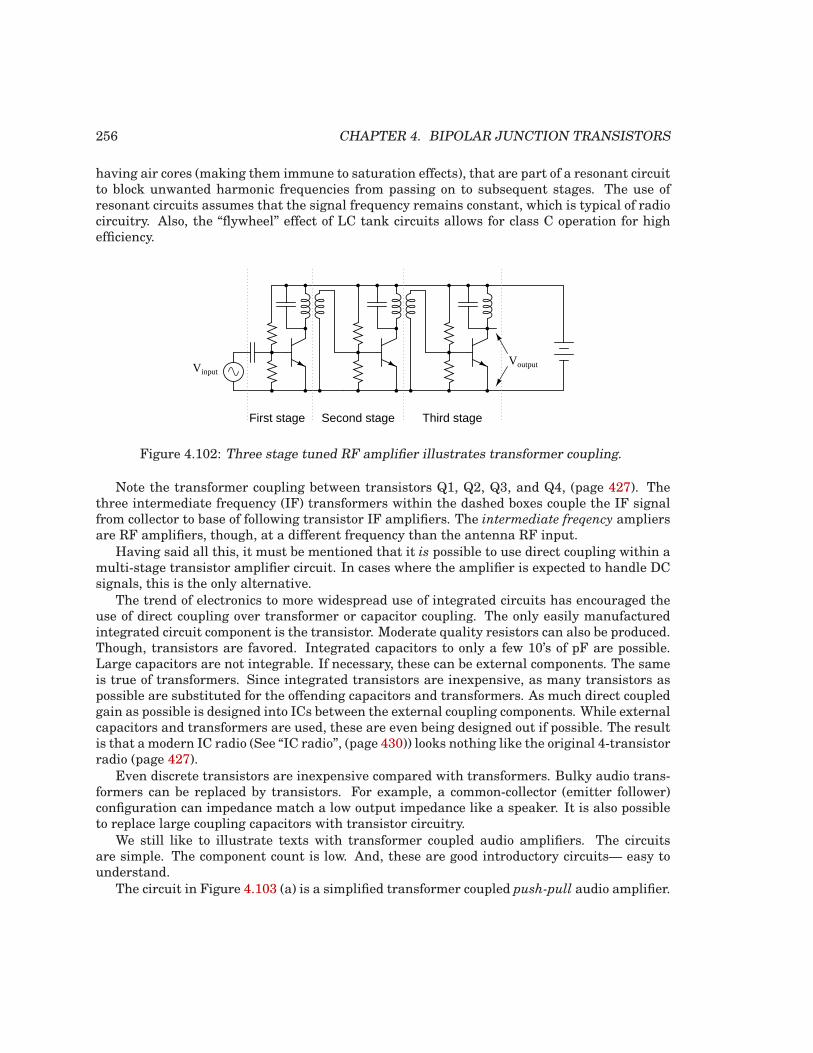
256 CHAPTER 4. BIPOLAR JUNCTION TRANSISTORS
having air cores (making them immune to saturation effects), that are part of a resonant circuitto block unwanted harmonic frequencies from passing on to subsequent stages. The use ofresonant circuits assumes that the signal frequency remains constant, which is typical of radiocircuitry. Also, the “flywheel” effect of LC tank circuits allows for class C operation for highefficiency.
VinputVoutput
First stage Second stage Third stage
Figure 4.102: Three stage tuned RF amplifier illustrates transformer coupling.
Note the transformer coupling between transistors Q1, Q2, Q3, and Q4, (page 427). Thethree intermediate frequency (IF) transformers within the dashed boxes couple the IF signalfrom collector to base of following transistor IF amplifiers. The intermediate freqency ampliersare RF amplifiers, though, at a different frequency than the antenna RF input.
Having said all this, it must be mentioned that it is possible to use direct coupling within amulti-stage transistor amplifier circuit. In cases where the amplifier is expected to handle DCsignals, this is the only alternative.
The trend of electronics to more widespread use of integrated circuits has encouraged theuse of direct coupling over transformer or capacitor coupling. The only easily manufacturedintegrated circuit component is the transistor. Moderate quality resistors can also be produced.Though, transistors are favored. Integrated capacitors to only a few 10’s of pF are possible.Large capacitors are not integrable. If necessary, these can be external components. The sameis true of transformers. Since integrated transistors are inexpensive, as many transistors aspossible are substituted for the offending capacitors and transformers. As much direct coupledgain as possible is designed into ICs between the external coupling components. While externalcapacitors and transformers are used, these are even being designed out if possible. The resultis that a modern IC radio (See “IC radio”, (page 430)) looks nothing like the original 4-transistorradio (page 427).
Even discrete transistors are inexpensive compared with transformers. Bulky audio trans-formers can be replaced by transistors. For example, a common-collector (emitter follower)configuration can impedance match a low output impedance like a speaker. It is also possibleto replace large coupling capacitors with transistor circuitry.
We still like to illustrate texts with transformer coupled audio amplifiers. The circuitsare simple. The component count is low. And, these are good introductory circuits— easy tounderstand.
The circuit in Figure 4.103 (a) is a simplified transformer coupled push-pull audio amplifier.
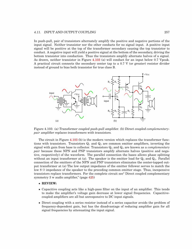
4.11. INPUT AND OUTPUT COUPLING 257
In push-pull, pair of transistors alternately amplify the positive and negative portions of theinput signal. Neither transistor nor the other conducts for no signal input. A positive inputsignal will be positive at the top of the transformer secondary causing the top transistor toconduct. A negative input will yield a positive signal at the bottom of the secondary, driving thebottom transistor into conduction. Thus the transistors amplify alternate halves of a signal.As drawn, neither transistor in Figure 4.103 (a) will conduct for an input below 0.7 Vpeak.A practical circuit connects the secondary center tap to a 0.7 V (or greater) resistor dividerinstead of ground to bias both transistor for true class B.
+Vcc
input
input
Q1
Q2Q3
Q4
+Vcc
(a) (b)
R1
R2
R3
R4 R5
Figure 4.103: (a) Transformer coupled push-pull amplifier. (b) Direct coupled complementary-
pair amplifier replaces transformers with transistors.
The circuit in Figure 4.103 (b) is the modern version which replaces the transformer func-tions with transistors. Transistors Q1 and Q2 are common emitter amplifiers, inverting thesignal with gain from base to collector. Transistors Q3 and Q4 are known as a complementary
pair because these NPN and PNP transistors amplify alternate halves (positive and nega-tive, respectively) of the waveform. The parallel connection the bases allows phase splittingwithout an input transformer at (a). The speaker is the emitter load for Q3 and Q4. Parallelconnection of the emitters of the NPN and PNP transistors eliminates the center-tapped out-put transformer at (a) The low output impedance of the emitter follower serves to match thelow 8 Ω impedance of the speaker to the preceding common emitter stage. Thus, inexpensivetransistors replace transformers. For the complete circuit see“ Direct coupled complementarysymmetry 3 w audio amplifier,” (page 425)
• REVIEW:
• Capacitive coupling acts like a high-pass filter on the input of an amplifier. This tendsto make the amplifier’s voltage gain decrease at lower signal frequencies. Capacitive-coupled amplifiers are all but unresponsive to DC input signals.
• Direct coupling with a series resistor instead of a series capacitor avoids the problem offrequency-dependent gain, but has the disadvantage of reducing amplifier gain for allsignal frequencies by attenuating the input signal.
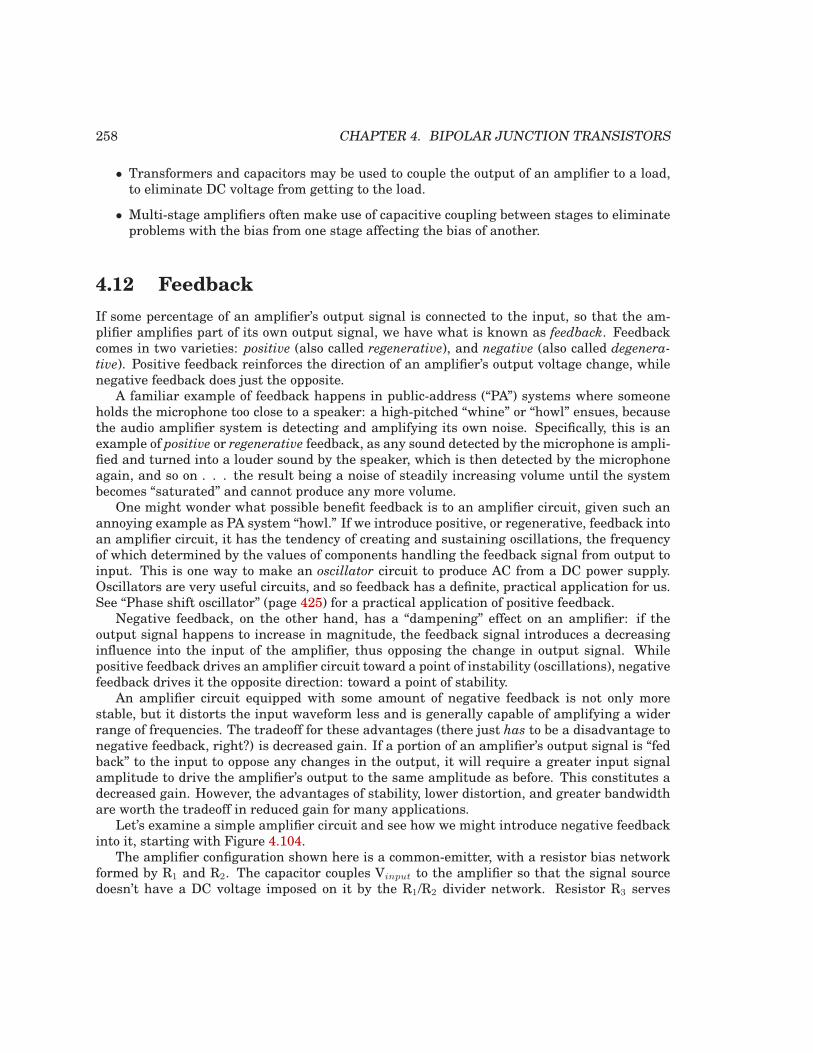
258 CHAPTER 4. BIPOLAR JUNCTION TRANSISTORS
• Transformers and capacitors may be used to couple the output of an amplifier to a load,to eliminate DC voltage from getting to the load.
• Multi-stage amplifiers often make use of capacitive coupling between stages to eliminateproblems with the bias from one stage affecting the bias of another.
4.12 Feedback
If some percentage of an amplifier’s output signal is connected to the input, so that the am-plifier amplifies part of its own output signal, we have what is known as feedback. Feedbackcomes in two varieties: positive (also called regenerative), and negative (also called degenera-
tive). Positive feedback reinforces the direction of an amplifier’s output voltage change, whilenegative feedback does just the opposite.
A familiar example of feedback happens in public-address (“PA”) systems where someoneholds the microphone too close to a speaker: a high-pitched “whine” or “howl” ensues, becausethe audio amplifier system is detecting and amplifying its own noise. Specifically, this is anexample of positive or regenerative feedback, as any sound detected by the microphone is ampli-fied and turned into a louder sound by the speaker, which is then detected by the microphoneagain, and so on . . . the result being a noise of steadily increasing volume until the systembecomes “saturated” and cannot produce any more volume.
One might wonder what possible benefit feedback is to an amplifier circuit, given such anannoying example as PA system “howl.” If we introduce positive, or regenerative, feedback intoan amplifier circuit, it has the tendency of creating and sustaining oscillations, the frequencyof which determined by the values of components handling the feedback signal from output toinput. This is one way to make an oscillator circuit to produce AC from a DC power supply.Oscillators are very useful circuits, and so feedback has a definite, practical application for us.See “Phase shift oscillator” (page 425) for a practical application of positive feedback.
Negative feedback, on the other hand, has a “dampening” effect on an amplifier: if theoutput signal happens to increase in magnitude, the feedback signal introduces a decreasinginfluence into the input of the amplifier, thus opposing the change in output signal. Whilepositive feedback drives an amplifier circuit toward a point of instability (oscillations), negativefeedback drives it the opposite direction: toward a point of stability.
An amplifier circuit equipped with some amount of negative feedback is not only morestable, but it distorts the input waveform less and is generally capable of amplifying a widerrange of frequencies. The tradeoff for these advantages (there just has to be a disadvantage tonegative feedback, right?) is decreased gain. If a portion of an amplifier’s output signal is “fedback” to the input to oppose any changes in the output, it will require a greater input signalamplitude to drive the amplifier’s output to the same amplitude as before. This constitutes adecreased gain. However, the advantages of stability, lower distortion, and greater bandwidthare worth the tradeoff in reduced gain for many applications.
Let’s examine a simple amplifier circuit and see how we might introduce negative feedbackinto it, starting with Figure 4.104.
The amplifier configuration shown here is a common-emitter, with a resistor bias networkformed by R1 and R2. The capacitor couples Vinput to the amplifier so that the signal sourcedoesn’t have a DC voltage imposed on it by the R1/R2 divider network. Resistor R3 serves
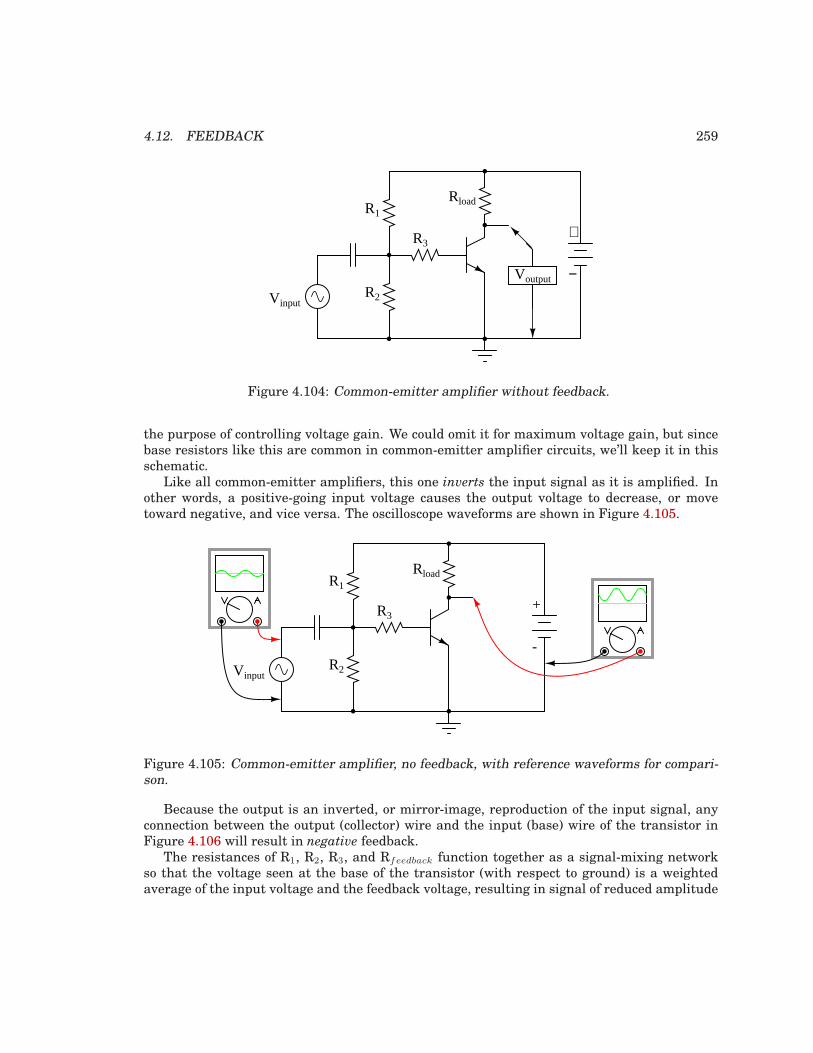
4.12. FEEDBACK 259
Rload
Vinput
R1
R2
R3
Voutput
+
−
Figure 4.104: Common-emitter amplifier without feedback.
the purpose of controlling voltage gain. We could omit it for maximum voltage gain, but sincebase resistors like this are common in common-emitter amplifier circuits, we’ll keep it in thisschematic.
Like all common-emitter amplifiers, this one inverts the input signal as it is amplified. Inother words, a positive-going input voltage causes the output voltage to decrease, or movetoward negative, and vice versa. The oscilloscope waveforms are shown in Figure 4.105.
Rload
Vinput
R1
R2
R3+
-
Figure 4.105: Common-emitter amplifier, no feedback, with reference waveforms for compari-son.
Because the output is an inverted, or mirror-image, reproduction of the input signal, anyconnection between the output (collector) wire and the input (base) wire of the transistor inFigure 4.106 will result in negative feedback.
The resistances of R1, R2, R3, and Rfeedback function together as a signal-mixing networkso that the voltage seen at the base of the transistor (with respect to ground) is a weightedaverage of the input voltage and the feedback voltage, resulting in signal of reduced amplitude
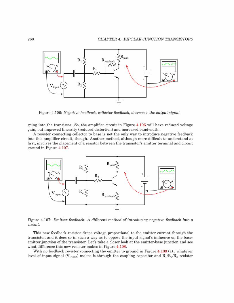
260 CHAPTER 4. BIPOLAR JUNCTION TRANSISTORS
Rload
Vinput
R1
R2
R3
Rfeedback
+
-
Figure 4.106: Negative feedback, collector feedback, decreases the output signal.
going into the transistor. So, the amplifier circuit in Figure 4.106 will have reduced voltagegain, but improved linearity (reduced distortion) and increased bandwidth.
A resistor connecting collector to base is not the only way to introduce negative feedbackinto this amplifier circuit, though. Another method, although more difficult to understand atfirst, involves the placement of a resistor between the transistor’s emitter terminal and circuitground in Figure 4.107.
Rload
Vinput
R1
R2
R3
Rfeedback
+
-
Figure 4.107: Emitter feedback: A different method of introducing negative feedback into acircuit.
This new feedback resistor drops voltage proportional to the emitter current through thetransistor, and it does so in such a way as to oppose the input signal’s influence on the base-emitter junction of the transistor. Let’s take a closer look at the emitter-base junction and seewhat difference this new resistor makes in Figure 4.108.
With no feedback resistor connecting the emitter to ground in Figure 4.108 (a) , whateverlevel of input signal (Vinput) makes it through the coupling capacitor and R1/R2/R3 resistor
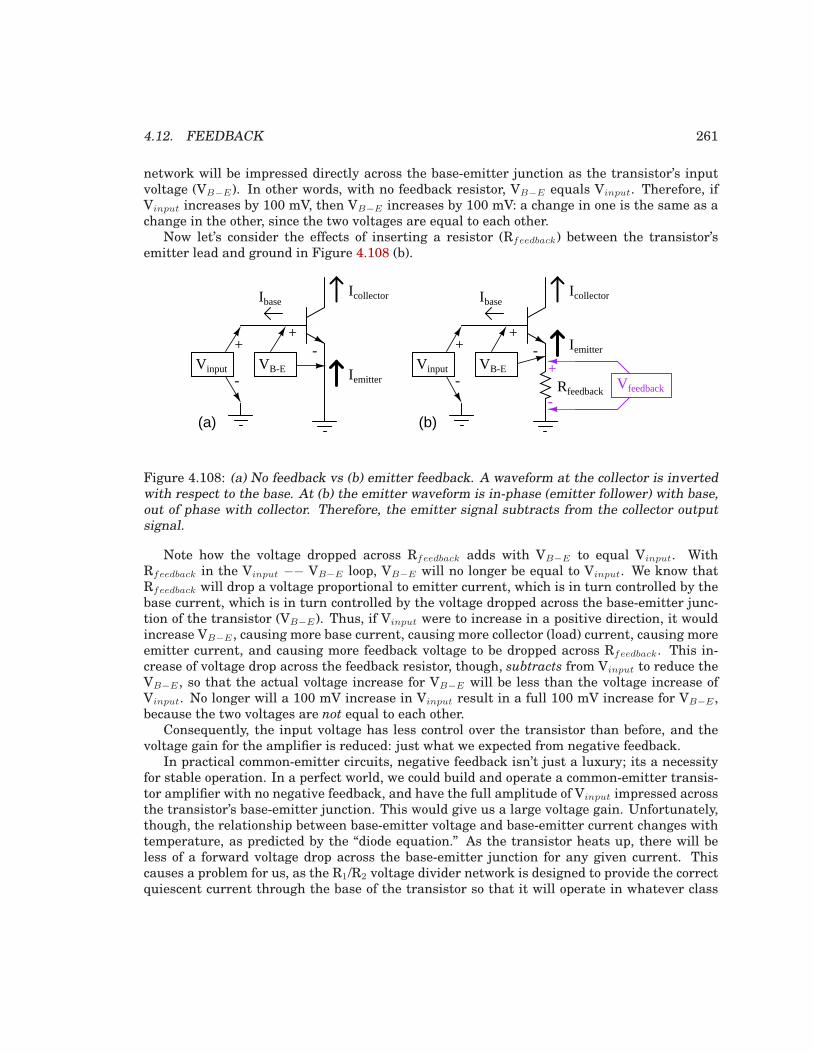
4.12. FEEDBACK 261
network will be impressed directly across the base-emitter junction as the transistor’s inputvoltage (VB−E). In other words, with no feedback resistor, VB−E equals Vinput. Therefore, ifVinput increases by 100 mV, then VB−E increases by 100 mV: a change in one is the same as achange in the other, since the two voltages are equal to each other.
Now let’s consider the effects of inserting a resistor (Rfeedback) between the transistor’semitter lead and ground in Figure 4.108 (b).
Vinput
+
-
Ibase
Iemitter
Icollector
+-
VB-E
(a)
Vinput
+
-
Ibase
Iemitter
Icollector
+-
VB-E
Rfeedback
+
-Vfeedback
(b)
Figure 4.108: (a) No feedback vs (b) emitter feedback. A waveform at the collector is invertedwith respect to the base. At (b) the emitter waveform is in-phase (emitter follower) with base,out of phase with collector. Therefore, the emitter signal subtracts from the collector outputsignal.
Note how the voltage dropped across Rfeedback adds with VB−E to equal Vinput. WithRfeedback in the Vinput −− VB−E loop, VB−E will no longer be equal to Vinput. We know thatRfeedback will drop a voltage proportional to emitter current, which is in turn controlled by thebase current, which is in turn controlled by the voltage dropped across the base-emitter junc-tion of the transistor (VB−E). Thus, if Vinput were to increase in a positive direction, it wouldincrease VB−E , causing more base current, causing more collector (load) current, causing moreemitter current, and causing more feedback voltage to be dropped across Rfeedback. This in-crease of voltage drop across the feedback resistor, though, subtracts from Vinput to reduce theVB−E , so that the actual voltage increase for VB−E will be less than the voltage increase ofVinput. No longer will a 100 mV increase in Vinput result in a full 100 mV increase for VB−E ,because the two voltages are not equal to each other.
Consequently, the input voltage has less control over the transistor than before, and thevoltage gain for the amplifier is reduced: just what we expected from negative feedback.
In practical common-emitter circuits, negative feedback isn’t just a luxury; its a necessityfor stable operation. In a perfect world, we could build and operate a common-emitter transis-tor amplifier with no negative feedback, and have the full amplitude of Vinput impressed acrossthe transistor’s base-emitter junction. This would give us a large voltage gain. Unfortunately,though, the relationship between base-emitter voltage and base-emitter current changes withtemperature, as predicted by the “diode equation.” As the transistor heats up, there will beless of a forward voltage drop across the base-emitter junction for any given current. Thiscauses a problem for us, as the R1/R2 voltage divider network is designed to provide the correctquiescent current through the base of the transistor so that it will operate in whatever class
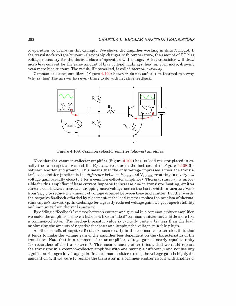
262 CHAPTER 4. BIPOLAR JUNCTION TRANSISTORS
of operation we desire (in this example, I’ve shown the amplifier working in class-A mode). Ifthe transistor’s voltage/current relationship changes with temperature, the amount of DC biasvoltage necessary for the desired class of operation will change. A hot transistor will drawmore bias current for the same amount of bias voltage, making it heat up even more, drawingeven more bias current. The result, if unchecked, is called thermal runaway.
Common-collector amplifiers, (Figure 4.109) however, do not suffer from thermal runaway.Why is this? The answer has everything to do with negative feedback.
RloadVinput
R1
R2
R3+
-
Figure 4.109: Common collector (emitter follower) amplifier.
Note that the common-collector amplifier (Figure 4.109) has its load resistor placed in ex-actly the same spot as we had the Rfeedback resistor in the last circuit in Figure 4.108 (b):between emitter and ground. This means that the only voltage impressed across the transis-tor’s base-emitter junction is the difference between Vinput and Voutput, resulting in a very lowvoltage gain (usually close to 1 for a common-collector amplifier). Thermal runaway is impos-sible for this amplifier: if base current happens to increase due to transistor heating, emittercurrent will likewise increase, dropping more voltage across the load, which in turn subtracts
from Vinput to reduce the amount of voltage dropped between base and emitter. In other words,the negative feedback afforded by placement of the load resistor makes the problem of thermalrunaway self-correcting. In exchange for a greatly reduced voltage gain, we get superb stabilityand immunity from thermal runaway.
By adding a “feedback” resistor between emitter and ground in a common-emitter amplifier,we make the amplifier behave a little less like an “ideal” common-emitter and a little more likea common-collector. The feedback resistor value is typically quite a bit less than the load,minimizing the amount of negative feedback and keeping the voltage gain fairly high.
Another benefit of negative feedback, seen clearly in the common-collector circuit, is thatit tends to make the voltage gain of the amplifier less dependent on the characteristics of thetransistor. Note that in a common-collector amplifier, voltage gain is nearly equal to unity(1), regardless of the transistor’s β. This means, among other things, that we could replacethe transistor in a common-collector amplifier with one having a different β and not see anysignificant changes in voltage gain. In a common-emitter circuit, the voltage gain is highly de-pendent on β. If we were to replace the transistor in a common-emitter circuit with another of
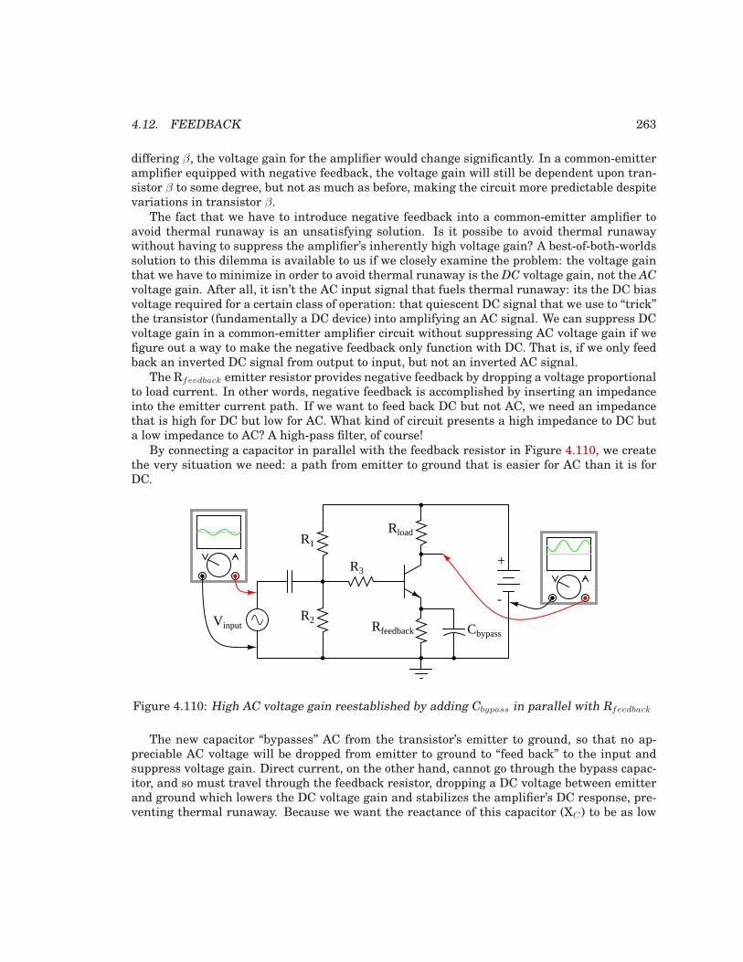
4.12. FEEDBACK 263
differing β, the voltage gain for the amplifier would change significantly. In a common-emitteramplifier equipped with negative feedback, the voltage gain will still be dependent upon tran-sistor β to some degree, but not as much as before, making the circuit more predictable despitevariations in transistor β.
The fact that we have to introduce negative feedback into a common-emitter amplifier toavoid thermal runaway is an unsatisfying solution. Is it possibe to avoid thermal runawaywithout having to suppress the amplifier’s inherently high voltage gain? A best-of-both-worldssolution to this dilemma is available to us if we closely examine the problem: the voltage gainthat we have to minimize in order to avoid thermal runaway is the DC voltage gain, not the ACvoltage gain. After all, it isn’t the AC input signal that fuels thermal runaway: its the DC biasvoltage required for a certain class of operation: that quiescent DC signal that we use to “trick”the transistor (fundamentally a DC device) into amplifying an AC signal. We can suppress DCvoltage gain in a common-emitter amplifier circuit without suppressing AC voltage gain if wefigure out a way to make the negative feedback only function with DC. That is, if we only feedback an inverted DC signal from output to input, but not an inverted AC signal.
The Rfeedback emitter resistor provides negative feedback by dropping a voltage proportionalto load current. In other words, negative feedback is accomplished by inserting an impedanceinto the emitter current path. If we want to feed back DC but not AC, we need an impedancethat is high for DC but low for AC. What kind of circuit presents a high impedance to DC buta low impedance to AC? A high-pass filter, of course!
By connecting a capacitor in parallel with the feedback resistor in Figure 4.110, we createthe very situation we need: a path from emitter to ground that is easier for AC than it is forDC.
Rload
Vinput
R1
R2
R3
Rfeedback Cbypass
+
-
Figure 4.110: High AC voltage gain reestablished by adding Cbypass in parallel with Rfeedback
The new capacitor “bypasses” AC from the transistor’s emitter to ground, so that no ap-preciable AC voltage will be dropped from emitter to ground to “feed back” to the input andsuppress voltage gain. Direct current, on the other hand, cannot go through the bypass capac-itor, and so must travel through the feedback resistor, dropping a DC voltage between emitterand ground which lowers the DC voltage gain and stabilizes the amplifier’s DC response, pre-venting thermal runaway. Because we want the reactance of this capacitor (XC) to be as low
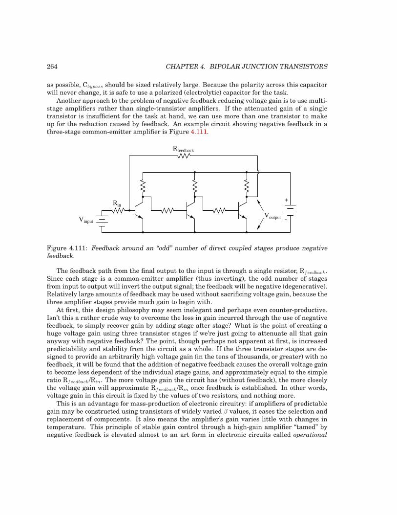
264 CHAPTER 4. BIPOLAR JUNCTION TRANSISTORS
as possible, Cbypass should be sized relatively large. Because the polarity across this capacitorwill never change, it is safe to use a polarized (electrolytic) capacitor for the task.
Another approach to the problem of negative feedback reducing voltage gain is to use multi-stage amplifiers rather than single-transistor amplifiers. If the attenuated gain of a singletransistor is insufficient for the task at hand, we can use more than one transistor to makeup for the reduction caused by feedback. An example circuit showing negative feedback in athree-stage common-emitter amplifier is Figure 4.111.
VinputVoutput
Rin
Rfeedback
+
-
Figure 4.111: Feedback around an “odd” number of direct coupled stages produce negativefeedback.
The feedback path from the final output to the input is through a single resistor, Rfeedback.Since each stage is a common-emitter amplifier (thus inverting), the odd number of stagesfrom input to output will invert the output signal; the feedback will be negative (degenerative).Relatively large amounts of feedback may be used without sacrificing voltage gain, because thethree amplifier stages provide much gain to begin with.
At first, this design philosophy may seem inelegant and perhaps even counter-productive.Isn’t this a rather crude way to overcome the loss in gain incurred through the use of negativefeedback, to simply recover gain by adding stage after stage? What is the point of creating ahuge voltage gain using three transistor stages if we’re just going to attenuate all that gainanyway with negative feedback? The point, though perhaps not apparent at first, is increasedpredictability and stability from the circuit as a whole. If the three transistor stages are de-signed to provide an arbitrarily high voltage gain (in the tens of thousands, or greater) with nofeedback, it will be found that the addition of negative feedback causes the overall voltage gainto become less dependent of the individual stage gains, and approximately equal to the simpleratio Rfeedback/Rin. The more voltage gain the circuit has (without feedback), the more closelythe voltage gain will approximate Rfeedback/Rin once feedback is established. In other words,voltage gain in this circuit is fixed by the values of two resistors, and nothing more.
This is an advantage for mass-production of electronic circuitry: if amplifiers of predictablegain may be constructed using transistors of widely varied β values, it eases the selection andreplacement of components. It also means the amplifier’s gain varies little with changes intemperature. This principle of stable gain control through a high-gain amplifier “tamed” bynegative feedback is elevated almost to an art form in electronic circuits called operational
4.13. AMPLIFIER IMPEDANCES 265
amplifiers, or op-amps. You may read much more about these circuits in a later chapter of thisbook!
• REVIEW:
• Feedback is the coupling of an amplifier’s output to its input.
• Positive, or regenerative feedback has the tendency of making an amplifier circuit unsta-ble, so that it produces oscillations (AC). The frequency of these oscillations is largelydetermined by the components in the feedback network.
• Negative, or degenerative feedback has the tendency of making an amplifier circuit morestable, so that its output changes less for a given input signal than without feedback.This reduces the gain of the amplifier, but has the advantage of decreasing distortion andincreasing bandwidth (the range of frequencies the amplifier can handle).
• Negative feedback may be introduced into a common-emitter circuit by coupling collectorto base, or by inserting a resistor between emitter and ground.
• An emitter-to-ground “feedback” resistor is usually found in common-emitter circuits asa preventative measure against thermal runaway.
• Negative feedback also has the advantage of making amplifier voltage gain more depen-dent on resistor values and less dependent on the transistor’s characteristics.
• Common-collector amplifiers have much negative feedback, due to the placement of theload resistor between emitter and ground. This feedback accounts for the extremely sta-ble voltage gain of the amplifier, as well as its immunity against thermal runaway.
• Voltage gain for a common-emitter circuit may be re-established without sacrificing im-munity to thermal runaway, by connecting a bypass capacitor in parallel with the emitter“feedback resistor.”
• If the voltage gain of an amplifier is arbitrarily high (tens of thousands, or greater), andnegative feedback is used to reduce the gain to reasonable levels, it will be found thatthe gain will approximately equal Rfeedback/Rin. Changes in transistor β or other inter-nal component values will have little effect on voltage gain with feedback in operation,resulting in an amplifier that is stable and easy to design.
4.13 Amplifier impedances
Input impedance varies considerably with the circuit configuration shown in Figure 4.112. Italso varies with biasing. Not considered here, the input impedance is complex and varies withfrequency. For the common-emitter and common-collector it is base resistance times β. Thebase resistance can be both internal and external to the transistor. For the common-collector:
Rin = βRE
It is a bit more complicated for the common-emitter circuit. We need to know the internalemitter resistance rEE . This is given by:
266 CHAPTER 4. BIPOLAR JUNCTION TRANSISTORS
r EE = KT/I Emwhere:
K=1.38 ×10⁻²³ watt-sec/ oC, Boltzman’s constantT= temperature in Kelvins ∼=300.I E = emitter currentm = varies from 1 to 2 for Silicon
RE∼= 0.026V/I E = 26mV/I E
Thus, for the common-emitter circuit Rin isRin = βr EE
As an example the input resistance of a, β = 100, CE configuration biased at 1 mA is:rEE = 26mV/1mA = 26Ω
Rin = βr EE = 100(26) = 2600 ΩMoreover, a more accurate Rin for the common-collector should have included rEE
Rin = β(R E + r EE)This equation (above) is also applicable to a common-emitter configuration with an emitter
resistor.Input impedance for the common-base configuration is Rin = rEE .The high input impedance of the common-collector configuration matches high impedance
sources. A crystal or ceramic microphone is one such high impedance source. The common-base arrangement is sometimes used in RF (radio frequency) circuits to match a low impedancesource, for example, a 50 Ω coaxial cable feed. For moderate impedance sources, the common-emitter is a good match. An example is a dynamic microphone.
The output impedances of the three basic configurations are listed in Figure 4.112. Themoderate output impedance of the common-emitter configuration helps make it a popularchoice for general use. The Low output impedance of the common-collector is put to gooduse in impedance matching, for example, tranformerless matching to a 4 Ohm speaker. Theredo not appear to be any simple formulas for the output impedances. However, R. Victor Jonesdevelops expressions for output resistance. [3]
• REVIEW:
• See Figure 4.112.
4.14 Current mirrors
An often-used circuit applying the bipolar junction transistor is the so-called current mirror,which serves as a simple current regulator, supplying nearly constant current to a load over awide range of load resistances.
We know that in a transistor operating in its active mode, collector current is equal to basecurrent multiplied by the ratio β. We also know that the ratio between collector current andemitter current is called α. Because collector current is equal to base current multiplied by β,and emitter current is the sum of the base and collector currents, α should be mathematicallyderivable from β. If you do the algebra, you’ll find that α = β/(β+1) for any transistor.
We’ve seen already how maintaining a constant base current through an active transistorresults in the regulation of collector current, according to the β ratio. Well, the α ratio works
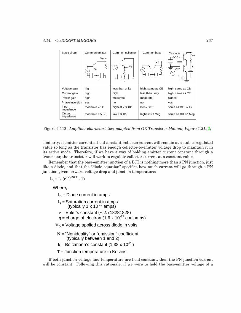
4.14. CURRENT MIRRORS 267
Voltage gain
Current gain
Power gain
Phase inversionInput impedanceOutput impedance
Common emitter Common collector Common base
less than unity
yes no no
moderate ≈ 1k
high
moderate
less than unity
high
highest ≈ 300k low ≈ 50Ω
highest ≈ 1Meglow ≈ 300Ωmoderate ≈ 50 k
moderate
high, same as CE
high
VoVo
Vo
high
Basic circuit
++ + ++ +-- --
--
Vo
+
+
+
Cascode
high, same as CB
high, same as CE
yes
same as CE, ≈ 1k
same as CB,≈1Meg
highest
Figure 4.112: Amplifier characteristics, adapted from GE Transistor Manual, Figure 1.21.[2]
similarly: if emitter current is held constant, collector current will remain at a stable, regulatedvalue so long as the transistor has enough collector-to-emitter voltage drop to maintain it inits active mode. Therefore, if we have a way of holding emitter current constant through atransistor, the transistor will work to regulate collector current at a constant value.
Remember that the base-emitter junction of a BJT is nothing more than a PN junction, justlike a diode, and that the “diode equation” specifies how much current will go through a PNjunction given forward voltage drop and junction temperature:
ID = IS (eqVD/NkT - 1)
Where,
ID = Diode current in amps
IS = Saturation current in amps
e = Euler’s constant (~ 2.718281828)q = charge of electron (1.6 x 10⁻¹⁹ coulombs)
VD = Voltage applied across diode in volts
N = "Nonideality" or "emission" coefficient
(typically 1 x 10-12 amps)
(typically between 1 and 2)
T = Junction temperature in Kelvins
k = Boltzmann’s constant (1.38 x 10⁻²³)
If both junction voltage and temperature are held constant, then the PN junction currentwill be constant. Following this rationale, if we were to hold the base-emitter voltage of a
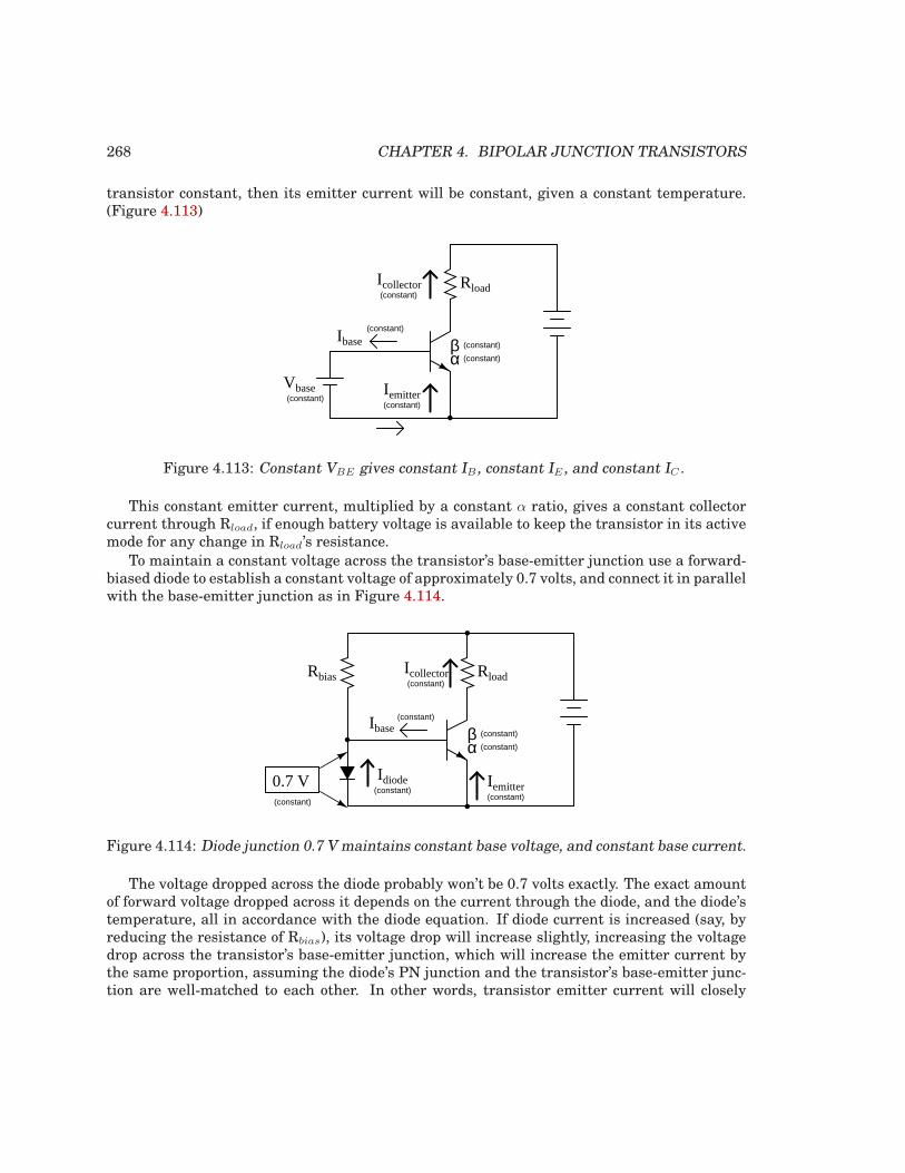
268 CHAPTER 4. BIPOLAR JUNCTION TRANSISTORS
transistor constant, then its emitter current will be constant, given a constant temperature.(Figure 4.113)
Rload
Vbase(constant)
(constant)
β (constant)
Icollector(constant)
Ibase
Iemitter(constant)
α (constant)
Figure 4.113: Constant VBE gives constant IB, constant IE , and constant IC .
This constant emitter current, multiplied by a constant α ratio, gives a constant collectorcurrent through Rload, if enough battery voltage is available to keep the transistor in its activemode for any change in Rload’s resistance.
To maintain a constant voltage across the transistor’s base-emitter junction use a forward-biased diode to establish a constant voltage of approximately 0.7 volts, and connect it in parallelwith the base-emitter junction as in Figure 4.114.
Rload
(constant)
Ibase(constant)
β (constant)
Icollector(constant)
0.7 V Idiode(constant)
Iemitter(constant)
α (constant)
Rbias
Figure 4.114: Diode junction 0.7 V maintains constant base voltage, and constant base current.
The voltage dropped across the diode probably won’t be 0.7 volts exactly. The exact amountof forward voltage dropped across it depends on the current through the diode, and the diode’stemperature, all in accordance with the diode equation. If diode current is increased (say, byreducing the resistance of Rbias), its voltage drop will increase slightly, increasing the voltagedrop across the transistor’s base-emitter junction, which will increase the emitter current bythe same proportion, assuming the diode’s PN junction and the transistor’s base-emitter junc-tion are well-matched to each other. In other words, transistor emitter current will closely
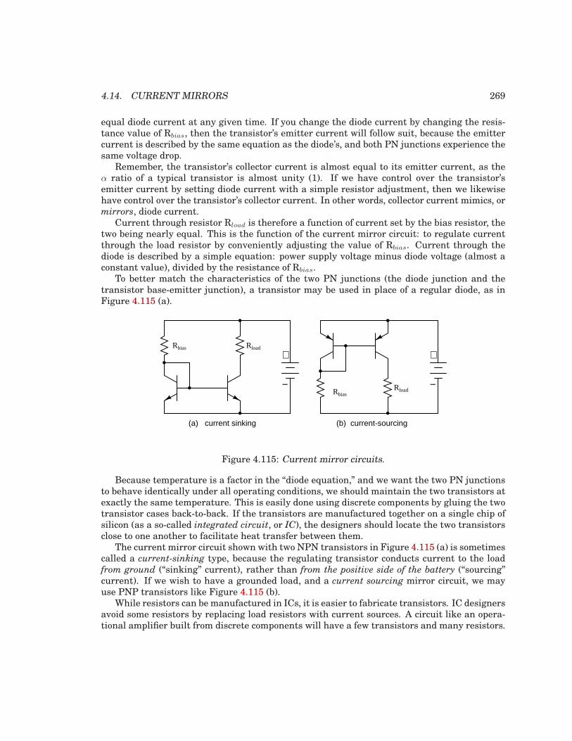
4.14. CURRENT MIRRORS 269
equal diode current at any given time. If you change the diode current by changing the resis-tance value of Rbias, then the transistor’s emitter current will follow suit, because the emittercurrent is described by the same equation as the diode’s, and both PN junctions experience thesame voltage drop.
Remember, the transistor’s collector current is almost equal to its emitter current, as theα ratio of a typical transistor is almost unity (1). If we have control over the transistor’semitter current by setting diode current with a simple resistor adjustment, then we likewisehave control over the transistor’s collector current. In other words, collector current mimics, ormirrors, diode current.
Current through resistor Rload is therefore a function of current set by the bias resistor, thetwo being nearly equal. This is the function of the current mirror circuit: to regulate currentthrough the load resistor by conveniently adjusting the value of Rbias. Current through thediode is described by a simple equation: power supply voltage minus diode voltage (almost aconstant value), divided by the resistance of Rbias.
To better match the characteristics of the two PN junctions (the diode junction and thetransistor base-emitter junction), a transistor may be used in place of a regular diode, as inFigure 4.115 (a).
RloadRbias
(a) current sinking
+
− RloadRbias
(b) current-sourcing
+
−
Figure 4.115: Current mirror circuits.
Because temperature is a factor in the “diode equation,” and we want the two PN junctionsto behave identically under all operating conditions, we should maintain the two transistors atexactly the same temperature. This is easily done using discrete components by gluing the twotransistor cases back-to-back. If the transistors are manufactured together on a single chip ofsilicon (as a so-called integrated circuit, or IC), the designers should locate the two transistorsclose to one another to facilitate heat transfer between them.
The current mirror circuit shown with two NPN transistors in Figure 4.115 (a) is sometimescalled a current-sinking type, because the regulating transistor conducts current to the loadfrom ground (“sinking” current), rather than from the positive side of the battery (“sourcing”current). If we wish to have a grounded load, and a current sourcing mirror circuit, we mayuse PNP transistors like Figure 4.115 (b).
While resistors can be manufactured in ICs, it is easier to fabricate transistors. IC designersavoid some resistors by replacing load resistors with current sources. A circuit like an opera-tional amplifier built from discrete components will have a few transistors and many resistors.
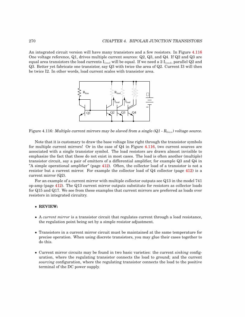
270 CHAPTER 4. BIPOLAR JUNCTION TRANSISTORS
An integrated circuit version will have many transistors and a few resistors. In Figure 4.116One voltage reference, Q1, drives multiple current sources: Q2, Q3, and Q4. If Q2 and Q3 areequal area transistors the load currents Iload will be equal. If we need a 2·Iload, parallel Q2 andQ3. Better yet fabricate one transistor, say Q3 with twice the area of Q2. Current I3 will thenbe twice I2. In other words, load current scales with transistor area.
RloadRbias +
−Q1 Q2 Q3 Q4
Iload Iload
Figure 4.116: Multiple current mirrors may be slaved from a single (Q1 - Rbias) voltage source.
Note that it is customary to draw the base voltage line right through the transistor symbolsfor multiple current mirrors! Or in the case of Q4 in Figure 4.116, two current sources areassociated with a single transistor symbol. The load resistors are drawn almost invisible toemphasize the fact that these do not exist in most cases. The load is often another (multiple)transistor circuit, say a pair of emitters of a differential amplifier, for example Q3 and Q4 in”A simple operational amplifier” (page 412). Often, the collector load of a transistor is not aresistor but a current mirror. For example the collector load of Q4 collector (page 412) is acurrent mirror (Q2).
For an example of a current mirror with multiple collector outputs see Q13 in the model 741op-amp (page 412). The Q13 current mirror outputs substitute for resistors as collector loadsfor Q15 and Q17. We see from these examples that current mirrors are preferred as loads overresistors in integrated circuitry.
• REVIEW:
• A current mirror is a transistor circuit that regulates current through a load resistance,the regulation point being set by a simple resistor adjustment.
• Transistors in a current mirror circuit must be maintained at the same temperature forprecise operation. When using discrete transistors, you may glue their cases together todo this.
• Current mirror circuits may be found in two basic varieties: the current sinking config-uration, where the regulating transistor connects the load to ground; and the currentsourcing configuration, where the regulating transistor connects the load to the positiveterminal of the DC power supply.
4.15. TRANSISTOR RATINGS AND PACKAGES 271
4.15 Transistor ratings and packages
Like all electrical and electronic components, transistors are limited in the amounts of volt-age and current each one can handle without sustaining damage. Since transistors are morecomplex than some of the other components you’re used to seeing at this point, these tend tohave more kinds of ratings. What follows is an itemized description of some typical transistorratings.
Power dissipation: When a transistor conducts current between collector and emitter, it alsodrops voltage between those two points. At any given time, the power dissipated by a transis-tor is equal to the product (multiplication) of collector current and collector-emitter voltage.Just like resistors, transistors are rated for how many watts each can safely dissipate with-out sustaining damage. High temperature is the mortal enemy of all semiconductor devices,and bipolar transistors tend to be more susceptible to thermal damage than most. Power rat-ings are always referenced to the temperature of ambient (surrounding) air. When transistorsare to be used in hotter environments (>25o, their power ratings must be derated to avoid ashortened service life.
Reverse voltages: As with diodes, bipolar transistors are rated for maximum allowablereverse-bias voltage across their PN junctions. This includes voltage ratings for the emitter-base junction VEB , collector-base junction VCB , and also from collector to emitter VCE .
VEB , the maximum reverse voltage from emitter to base is approximately 7 V for somesmall signal transistors. Some circuit designers use discrete BJTs as 7 V zener diodes witha series current limiting resistor. Transistor inputs to analog integrated circuits also have aVEB rating, which if exceeded will cause damage, no zenering of the inputs is allowed.
The rating for maximum collector-emitter voltage VCE can be thought of as the maximumvoltage it can withstand while in full-cutoff mode (no base current). This rating is of particularimportance when using a bipolar transistor as a switch. A typical value for a small signal tran-sistor is 60 to 80 V. In power transistors, this could range to 1000 V, for example, a horizontaldeflection transistor in a cathode ray tube display.
Collector current: A maximum value for collector current IC will be given by the manufac-turer in amps. Typical values for small signal transistors are 10s to 100s of mA, 10s of A forpower transistors. Understand that this maximum figure assumes a saturated state (mini-mum collector-emitter voltage drop). If the transistor is not saturated, and in fact is droppingsubstantial voltage between collector and emitter, the maximum power dissipation rating willprobably be exceeded before the maximum collector current rating. Just something to keep inmind when designing a transistor circuit!
Saturation voltages: Ideally, a saturated transistor acts as a closed switch contact betweencollector and emitter, dropping zero voltage at full collector current. In reality this is never
true. Manufacturers will specify the maximum voltage drop of a transistor at saturation, bothbetween the collector and emitter, and also between base and emitter (forward voltage dropof that PN junction). Collector-emitter voltage drop at saturation is generally expected to be0.3 volts or less, but this figure is of course dependent on the specific type of transistor. Lowvoltage transistors, low VCE , show lower saturation voltages. The saturation voltage is alsolower for higher base drive current.
Base-emitter forward voltage drop, kVBE , is similar to that of an equivalent diode, ∼=0.7 V,which should come as no surprise.
Beta: The ratio of collector current to base current, β is the fundamental parameter char-
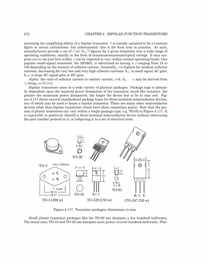
272 CHAPTER 4. BIPOLAR JUNCTION TRANSISTORS
acterizing the amplifying ability of a bipolar transistor. β is usually assumed to be a constantfigure in circuit calculations, but unfortunately this is far from true in practice. As such,manufacturers provide a set of β (or “hfe”) figures for a given transistor over a wide range ofoperating conditions, usually in the form of maximum/minimum/typical ratings. It may sur-prise you to see just how widely β can be expected to vary within normal operating limits. Onepopular small-signal transistor, the 2N3903, is advertised as having a β ranging from 15 to150 depending on the amount of collector current. Generally, β is highest for medium collectorcurrents, decreasing for very low and very high collector currents. hfe is small signal AC gain;hFE is large AC signal gain or DC gain.
Alpha: the ratio of collector current to emitter current, α=IC /IE . α may be derived fromβ, being α=β/(β+1) .
Bipolar transistors come in a wide variety of physical packages. Package type is primar-ily dependent upon the required power dissipation of the transistor, much like resistors: thegreater the maximum power dissipation, the larger the device has to be to stay cool. Fig-ure 4.117 shows several standardized package types for three-terminal semiconductor devices,any of which may be used to house a bipolar transistor. There are many other semiconductordevices other than bipolar transistors which have three connection points. Note that the pin-outs of plastic transistors can vary within a single package type, e.g. TO-92 in Figure 4.117. Itis impossible to positively identify a three-terminal semiconductor device without referencingthe part number printed on it, or subjecting it to a set of electrical tests.
30.1516.89
39.37
B
E
case, CollectorTO-3
Β C E
TO-3 (300 w) (TO-247 250 w)TO-220 (150 w)B C E
16
2110.7
15.5
5.3
5.2
TO-92
Β CE
9.4
6.6
Β CE
TO-18
TO-39
5.8
5.3
Β CE
ΒCE
Figure 4.117: Transistor packages, dimensions in mm.
Small plastic transistor packages like the TO-92 can dissipate a few hundred milliwatts.The metal cans, TO-18 and TO-39 can dissipate more power, several hundred milliwatts. Plas-
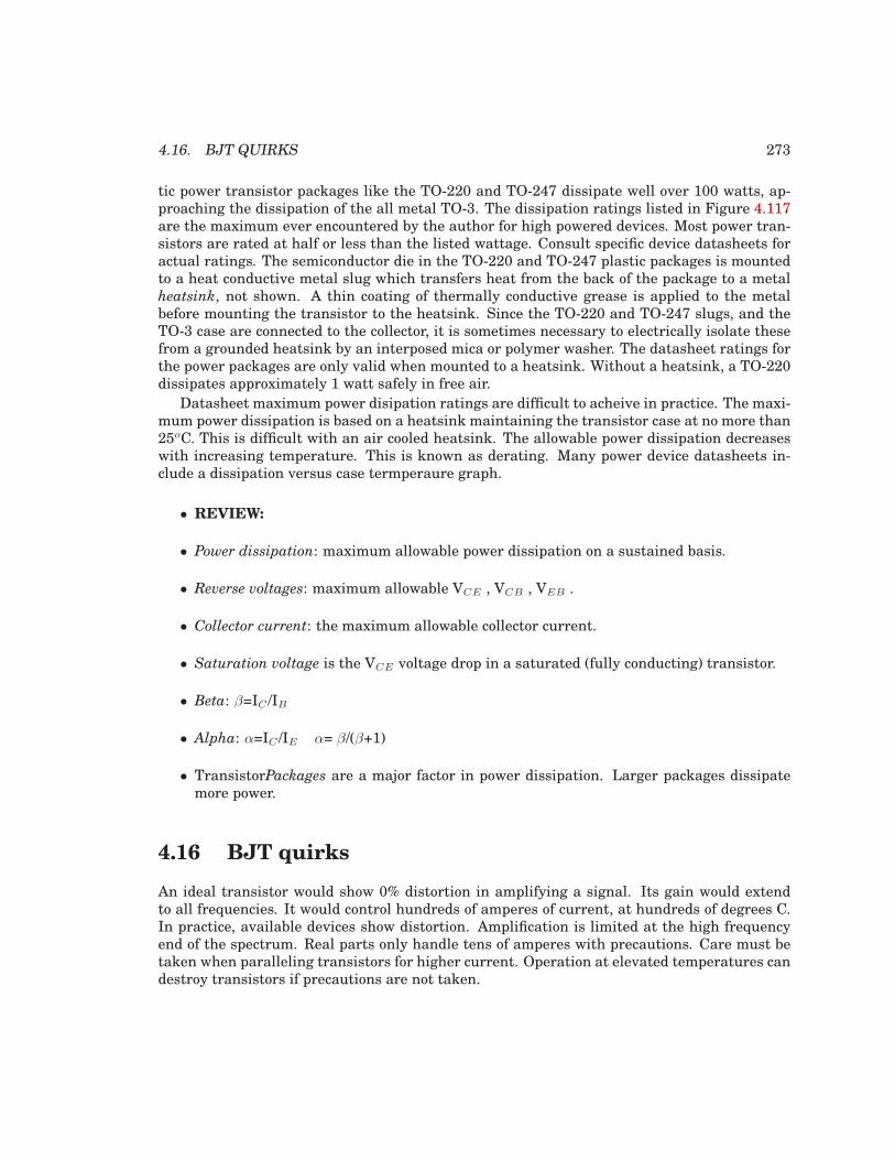
4.16. BJT QUIRKS 273
tic power transistor packages like the TO-220 and TO-247 dissipate well over 100 watts, ap-proaching the dissipation of the all metal TO-3. The dissipation ratings listed in Figure 4.117are the maximum ever encountered by the author for high powered devices. Most power tran-sistors are rated at half or less than the listed wattage. Consult specific device datasheets foractual ratings. The semiconductor die in the TO-220 and TO-247 plastic packages is mountedto a heat conductive metal slug which transfers heat from the back of the package to a metalheatsink, not shown. A thin coating of thermally conductive grease is applied to the metalbefore mounting the transistor to the heatsink. Since the TO-220 and TO-247 slugs, and theTO-3 case are connected to the collector, it is sometimes necessary to electrically isolate thesefrom a grounded heatsink by an interposed mica or polymer washer. The datasheet ratings forthe power packages are only valid when mounted to a heatsink. Without a heatsink, a TO-220dissipates approximately 1 watt safely in free air.
Datasheet maximum power disipation ratings are difficult to acheive in practice. The maxi-mum power dissipation is based on a heatsink maintaining the transistor case at no more than25oC. This is difficult with an air cooled heatsink. The allowable power dissipation decreaseswith increasing temperature. This is known as derating. Many power device datasheets in-clude a dissipation versus case termperaure graph.
• REVIEW:
• Power dissipation: maximum allowable power dissipation on a sustained basis.
• Reverse voltages: maximum allowable VCE , VCB , VEB .
• Collector current: the maximum allowable collector current.
• Saturation voltage is the VCE voltage drop in a saturated (fully conducting) transistor.
• Beta: β=IC /IB
• Alpha: α=IC /IE α= β/(β+1)
• TransistorPackages are a major factor in power dissipation. Larger packages dissipatemore power.
4.16 BJT quirks
An ideal transistor would show 0% distortion in amplifying a signal. Its gain would extendto all frequencies. It would control hundreds of amperes of current, at hundreds of degrees C.In practice, available devices show distortion. Amplification is limited at the high frequencyend of the spectrum. Real parts only handle tens of amperes with precautions. Care must betaken when paralleling transistors for higher current. Operation at elevated temperatures candestroy transistors if precautions are not taken.
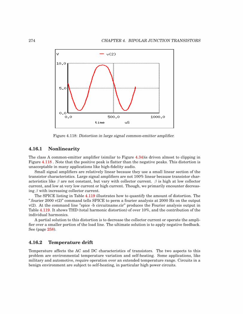
274 CHAPTER 4. BIPOLAR JUNCTION TRANSISTORS
Figure 4.118: Distortion in large signal common-emitter amplifier.
4.16.1 Nonlinearity
The class A common-emitter amplifier (similar to Figure 4.34)is driven almost to clipping inFigure 4.118 . Note that the positive peak is flatter than the negative peaks. This distortion isunacceptable in many applications like high-fidelity audio.
Small signal amplifiers are relatively linear because they use a small linear section of thetransistor characteristics. Large signal amplifiers are not 100% linear because transistor char-acteristics like β are not constant, but vary with collector current. β is high at low collectorcurrent, and low at very low current or high current. Though, we primarily encounter decreas-ing β with increasing collector current.
The SPICE listing in Table 4.119 illustrates how to quantify the amount of distortion. The”.fourier 2000 v(2)” command tells SPICE to perm a fourier analysis at 2000 Hz on the outputv(2). At the command line ”spice -b circuitname.cir” produces the Fourier analysis output inTable 4.119. It shows THD (total harmonic distortion) of over 10%, and the contribution of theindividual harmonics.
A partial solution to this distortion is to decrease the collector current or operate the ampli-fier over a smaller portion of the load line. The ultimate solution is to apply negative feedback.See (page 258).
4.16.2 Temperature drift
Temperature affects the AC and DC characteristics of transistors. The two aspects to thisproblem are environmental temperature variation and self-heating. Some applications, likemilitary and automotive, require operation over an extended temperature range. Circuits in abenign environment are subject to self-heating, in particular high power circuits.
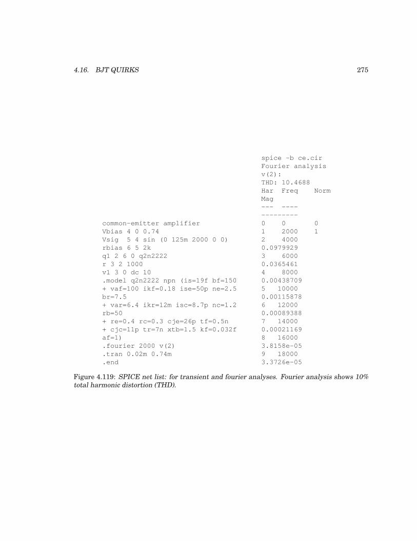
4.16. BJT QUIRKS 275
common-emitter amplifierVbias 4 0 0.74Vsig 5 4 sin (0 125m 2000 0 0)rbias 6 5 2kq1 2 6 0 q2n2222r 3 2 1000v1 3 0 dc 10.model q2n2222 npn (is=19f bf=150+ vaf=100 ikf=0.18 ise=50p ne=2.5br=7.5+ var=6.4 ikr=12m isc=8.7p nc=1.2rb=50+ re=0.4 rc=0.3 cje=26p tf=0.5n+ cjc=11p tr=7n xtb=1.5 kf=0.032faf=1).fourier 2000 v(2).tran 0.02m 0.74m.end
spice -b ce.cirFourier analysisv(2):THD: 10.4688Har Freq NormMag--- -------------0 0 01 2000 12 40000.09799293 60000.03654614 80000.004387095 100000.001158786 120000.000893887 140000.000211698 160003.8158e-059 180003.3726e-05
Figure 4.119: SPICE net list: for transient and fourier analyses. Fourier analysis shows 10%total harmonic distortion (THD).
276 CHAPTER 4. BIPOLAR JUNCTION TRANSISTORS
Leakage current ICO and β increase with temperature. The DC β hFE increases exponen-tially. The AC β hfe increases, but not as rapidly. It doubles over the range of -55o to 85o C. Astemperature increases, the increase in hfe will yield a larger common-emitter output, whichcould be clipped in extreme cases. The increase in hFE shifts the bias point, possibly clippingone peak. The shift in bias point is amplified in multi-stage direct-coupled amplifiers. Thesolution is some form of negative feedback to stabilize the bias point. This also stabilizes ACgain.
Increasing temperature in Figure 4.120 (a) will decrease VBE from the nominal 0.7V forsilicon transistors. Decreasing VBE increases collector current in a common-emitter amplifier,further shifting the bias point. The cure for shifting VBE is a pair of transistors configured asa differential amplifier. If both transistors in Figure 4.120 (b) are at the same temperature, theVBE will track with changing temperature and cancel.
+Vcc
-Vee
+Vcc
-Vee(a) (b)
VBE
+- VBE
+-
+- VBE
Figure 4.120: (a) single ended CE amplifier vs (b) differential amplifier with VBE cancellation.
The maximum recommended junction temperature for silicon devices is frequently 125o C.Though, this should be derated for higher reliability. Transistor action ceases beyond 150o C.Silicon carbide and diamond transistors will operate considerably higher.
4.16.3 Thermal runaway
The problem with increasing temperature causing increasing collector current is that more cur-rent increase the power dissipated by the transistor which, in turn, increases its temperature.This self-reinforcing cycle is known as thermal run away, which may destroy the transistor.Again, the solution is a bias scheme with some form of negative feedback to stabilize the biaspoint.
4.16.4 Junction capacitance
Capacitance exists between the terminals of a transistor. The collector-base capacitance CCB
and emitter-base capacitance CEB decrease the gain of a common emitter circuit at higherfrequencies.
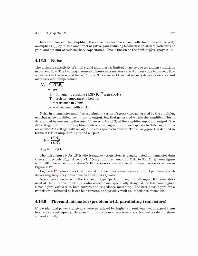
4.16. BJT QUIRKS 277
In a common emitter amplifier, the capacitive feedback from collector to base effectivelymultiplies CCB by β. The amount of negative gain-reducing feedback is related to both currentgain, and amount of collector-base capacitance. This is known as the Miller effect, (page 279).
4.16.5 Noise
The ultimate sensitivity of small signal amplifiers is limited by noise due to random variationsin current flow. The two major sources of noise in transistors are shot noise due to current flowof carriers in the base and thermal noise. The source of thermal noise is device resistance andincreases with temperature:
Vn = 4kTRBn
where
k = boltzman’s conatant (1.38•10−23 watt-sec/K)T = resistor tempeature in kelvinsR = resistance in Ohms
Bn = noise bandwidth in Hz
Noise in a transistor amplifier is defined in terms of excess noise generated by the amplifier,not that noise amplified from input to output, but that generated within the amplifier. This isdetermined by measuring the signal to noise ratio (S/N) at the amplifier input and output. TheAC voltage output of an amplifier with a small signal input corresponds to S+N, signal plusnoise. The AC voltage with no signal in corresponds to noise N. The noise figure F is defined interms of S/N of amplifier input and output:
FdB = 10 log F
F = (S/N)i
(S/N)o
The noise figure F for RF (radio frequency) transistors is usually listed on transistor datasheets in decibels, FdB . A good VHF (very high frequency, 30 MHz to 300 Mhz) noise figureis < 1 dB. The noise figure above VHF increases considerable, 20 dB per decade as shown inFigure 4.121.
Figure 4.121 also shows that noise at low frequencies increases at 10 dB per decade withdecreasing frequency. This noise is known as 1/f noise.
Noise figure varies with the transistor type (part number). Small signal RF transistorsused at the antenna input of a radio receiver are specifically designed for low noise figure.Noise figure varies with bias current and impedance matching. The best noise figure for atransistor is achieved at lower bias current, and possibly with an impedance mismatch.
4.16.6 Thermal mismatch (problem with paralleling transistors)
If two identical power transistors were paralleled for higher current, one would expect themto share current equally. Because of differences in characteristerics, transistors do not sharecurrent equally.
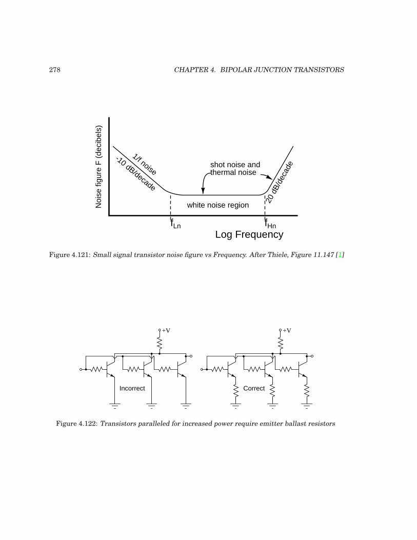
278 CHAPTER 4. BIPOLAR JUNCTION TRANSISTORS
Log Frequency
Noi
se fi
gure
F (
deci
bels
)
-10 dB/decade
20 d
B/de
cade
white noise region
1/f noiseshot noise andthermal noise
fLn fHn
Figure 4.121: Small signal transistor noise figure vs Frequency. After Thiele, Figure 11.147 [1]
+V +V
CorrectIncorrect
Figure 4.122: Transistors paralleled for increased power require emitter ballast resistors
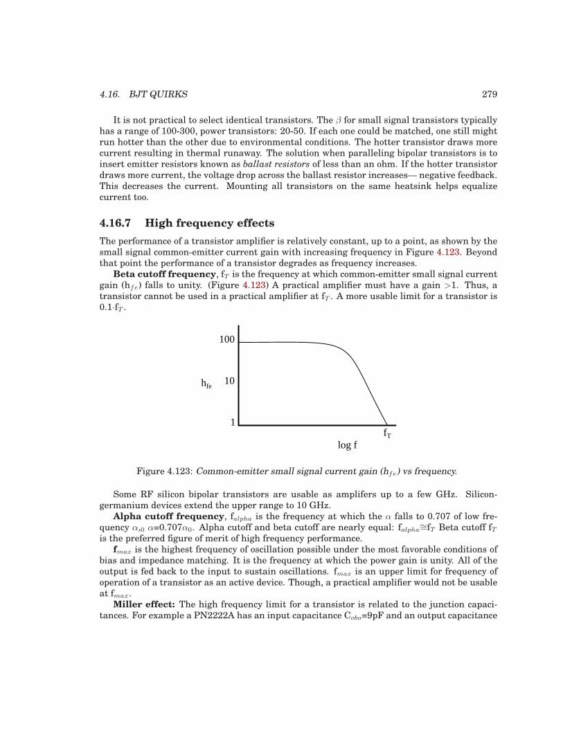
4.16. BJT QUIRKS 279
It is not practical to select identical transistors. The β for small signal transistors typicallyhas a range of 100-300, power transistors: 20-50. If each one could be matched, one still mightrun hotter than the other due to environmental conditions. The hotter transistor draws morecurrent resulting in thermal runaway. The solution when paralleling bipolar transistors is toinsert emitter resistors known as ballast resistors of less than an ohm. If the hotter transistordraws more current, the voltage drop across the ballast resistor increases— negative feedback.This decreases the current. Mounting all transistors on the same heatsink helps equalizecurrent too.
4.16.7 High frequency effects
The performance of a transistor amplifier is relatively constant, up to a point, as shown by thesmall signal common-emitter current gain with increasing frequency in Figure 4.123. Beyondthat point the performance of a transistor degrades as frequency increases.
Beta cutoff frequency, fT is the frequency at which common-emitter small signal currentgain (hfe) falls to unity. (Figure 4.123) A practical amplifier must have a gain >1. Thus, atransistor cannot be used in a practical amplifier at fT . A more usable limit for a transistor is0.1·fT .
1
100
10hfe
log ffT
Figure 4.123: Common-emitter small signal current gain (hfe) vs frequency.
Some RF silicon bipolar transistors are usable as amplifers up to a few GHz. Silicon-germanium devices extend the upper range to 10 GHz.
Alpha cutoff frequency, falpha is the frequency at which the α falls to 0.707 of low fre-quency α,0 α=0.707α0. Alpha cutoff and beta cutoff are nearly equal: falpha
∼=fT Beta cutoff fTis the preferred figure of merit of high frequency performance.
fmax is the highest frequency of oscillation possible under the most favorable conditions ofbias and impedance matching. It is the frequency at which the power gain is unity. All of theoutput is fed back to the input to sustain oscillations. fmax is an upper limit for frequency ofoperation of a transistor as an active device. Though, a practical amplifier would not be usableat fmax.
Miller effect: The high frequency limit for a transistor is related to the junction capaci-tances. For example a PN2222A has an input capacitance Cobo=9pF and an output capacitance
280 CHAPTER 4. BIPOLAR JUNCTION TRANSISTORS
Cibo=25pF from C-B and E-B respectively. [5] Although the C-E capacitance of 25 pF seemslarge, it is less of a factor than the C-B (9pF) capacitance. because of the Miller effect, the C-Bcapacitance has an effect on the base equivalent to beta times the capacitance in the common-emitter amplifier. Why might this be? A common-emitter amplifier inverts the signal frombase to collector. The inverted collector signal fed back to the base opposes the input on thebase. The collector signal is beta times larger than the input. For the PN2222A, β=50–300.Thus, the 9pF C-E capacitance looks like 9·50=450pF to 9·300=2700pF.
The solution to the junction capacitance problem is to select a high frequency transistor forwide bandwidth applications— RF (radio frequency) or microwave transistor. The bandwidthcan be extended further by using the common-base instead of the common-emitter configu-ration. The grounded base shields the emitter input from capacitive collector feedback. Atwo-transistor cascode arrangement will yield the same bandwidth as the common-base, withthe higher input impedance of the common-emitter.
• REVIEW:
• Transistor amplifiers exhibit distortion because of β variation with collector current.
• Ic, VBE , β and junction capacitance vary with temperature.
• An increase in temperature can cause an increase in IC , causing an increase in tempera-ture, a vicious cycle known as thermal runaway.
• Junction capacitance limits high frequency gain of a transistor. The Miller effect makesCcb look β times larger at the base of a CE amplifier.
• Transistor noise limits the ability to amplify small signals. Noise figure is a figure ofmerit concerning transistor noise.
• When paralleling power transistors for increased current, insert ballast resistors in serieswith the emitters to equalize current.
• FT is the absolute upper frequency limit for a CE amplifier, small signal current gainfalls to unity, hfe=1.
• Fmax is the upper frequency limit for an oscillator under the most ideal conditions.
Bibliography
[1] A. G. Thiele in Loyd P. Hunter, “Handbook of Semiconductor Electronics,” Low FrequencyAmplifiers, ISBN -07-031305-9, 1970
[2] “GE Transistor Manual”, General Electric, 1964.
[3] R. Victor Jones, “Basic BJT Amplifier Configurations”, November 7, 2001. athttp://people.seas.harvard.edu/˜jones/es154/lecture s/lecture 3/bjt amps/bjt amps.html
BIBLIOGRAPHY 281
[4] Tony Kuphaldt,“Lessons in Electric Circuits”, Vol. 1, DC, DC Network Analysis,Thevenin’s Theorem, at http://www.openbookproject.net/electricCircuits/DC/DC 10.html#xtocid102679
[5] “PN2222 Datasheet”,Fairchild Semiconductor Corporation, 2007 athttp://www.fairchildsemi.com/ds/PN/PN2222A.pdf

282 CHAPTER 4. BIPOLAR JUNCTION TRANSISTORS
Chapter 5
JUNCTION FIELD-EFFECT
TRANSISTORS
Contents
5.1 Introduction . . . . . . . . . . . . . . . . . . . . . . . . . . . . . . . . . . . . . . 283
5.2 The transistor as a switch . . . . . . . . . . . . . . . . . . . . . . . . . . . . . 285
5.3 Meter check of a transistor . . . . . . . . . . . . . . . . . . . . . . . . . . . . . 288
5.4 Active-mode operation . . . . . . . . . . . . . . . . . . . . . . . . . . . . . . . 290
5.5 The common-source amplifier – PENDING . . . . . . . . . . . . . . . . . . . 299
5.6 The common-drain amplifier – PENDING . . . . . . . . . . . . . . . . . . . . 300
5.7 The common-gate amplifier – PENDING . . . . . . . . . . . . . . . . . . . . 300
5.8 Biasing techniques – PENDING . . . . . . . . . . . . . . . . . . . . . . . . . . 300
5.9 Transistor ratings and packages – PENDING . . . . . . . . . . . . . . . . . 301
5.10 JFET quirks – PENDING . . . . . . . . . . . . . . . . . . . . . . . . . . . . . . 301
*** INCOMPLETE ***
5.1 Introduction
A transistor is a linear semiconductor device that controls current with the application of alower-power electrical signal. Transistors may be roughly grouped into two major divisions:bipolar and field-effect. In the last chapter we studied bipolar transistors, which utilize a smallcurrent to control a large current. In this chapter, we’ll introduce the general concept of thefield-effect transistor – a device utilizing a small voltage to control current – and then focuson one particular type: the junction field-effect transistor. In the next chapter we’ll exploreanother type of field-effect transistor, the insulated gate variety.
All field-effect transistors are unipolar rather than bipolar devices. That is, the main cur-rent through them is comprised either of electrons through an N-type semiconductor or holes
283
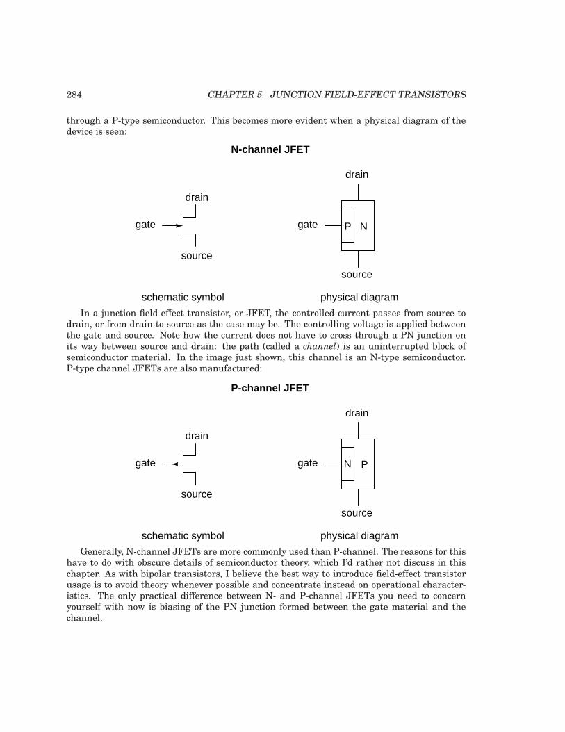
284 CHAPTER 5. JUNCTION FIELD-EFFECT TRANSISTORS
through a P-type semiconductor. This becomes more evident when a physical diagram of thedevice is seen:
schematic symbol physical diagram
P Ngate
drain
source
drain
source
gate
N-channel JFET
In a junction field-effect transistor, or JFET, the controlled current passes from source todrain, or from drain to source as the case may be. The controlling voltage is applied betweenthe gate and source. Note how the current does not have to cross through a PN junction onits way between source and drain: the path (called a channel) is an uninterrupted block ofsemiconductor material. In the image just shown, this channel is an N-type semiconductor.P-type channel JFETs are also manufactured:
schematic symbol physical diagram
PNgate
drain
source
drain
source
gate
P-channel JFET
Generally, N-channel JFETs are more commonly used than P-channel. The reasons for thishave to do with obscure details of semiconductor theory, which I’d rather not discuss in thischapter. As with bipolar transistors, I believe the best way to introduce field-effect transistorusage is to avoid theory whenever possible and concentrate instead on operational character-istics. The only practical difference between N- and P-channel JFETs you need to concernyourself with now is biasing of the PN junction formed between the gate material and thechannel.
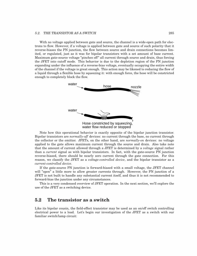
5.2. THE TRANSISTOR AS A SWITCH 285
With no voltage applied between gate and source, the channel is a wide-open path for elec-trons to flow. However, if a voltage is applied between gate and source of such polarity that itreverse-biases the PN junction, the flow between source and drain connections becomes lim-ited, or regulated, just as it was for bipolar transistors with a set amount of base current.Maximum gate-source voltage ”pinches off” all current through source and drain, thus forcingthe JFET into cutoff mode. This behavior is due to the depletion region of the PN junctionexpanding under the influence of a reverse-bias voltage, eventually occupying the entire widthof the channel if the voltage is great enough. This action may be likened to reducing the flow ofa liquid through a flexible hose by squeezing it: with enough force, the hose will be constrictedenough to completely block the flow.
waterhose nozzle
Hose constricted by squeezing,water flow reduced or stopped
water
Note how this operational behavior is exactly opposite of the bipolar junction transistor.Bipolar transistors are normally-off devices: no current through the base, no current throughthe collector or the emitter. JFETs, on the other hand, are normally-on devices: no voltageapplied to the gate allows maximum current through the source and drain. Also take notethat the amount of current allowed through a JFET is determined by a voltage signal ratherthan a current signal as with bipolar transistors. In fact, with the gate-source PN junctionreverse-biased, there should be nearly zero current through the gate connection. For thisreason, we classify the JFET as a voltage-controlled device, and the bipolar transistor as acurrent-controlled device.
If the gate-source PN junction is forward-biased with a small voltage, the JFET channelwill ”open” a little more to allow greater currents through. However, the PN junction of aJFET is not built to handle any substantial current itself, and thus it is not recommended toforward-bias the junction under any circumstances.
This is a very condensed overview of JFET operation. In the next section, we’ll explore theuse of the JFET as a switching device.
5.2 The transistor as a switch
Like its bipolar cousin, the field-effect transistor may be used as an on/off switch controllingelectrical power to a load. Let’s begin our investigation of the JFET as a switch with ourfamiliar switch/lamp circuit:
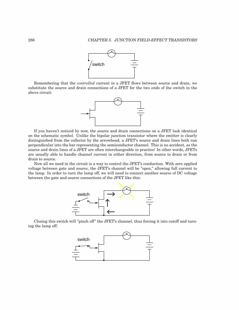
286 CHAPTER 5. JUNCTION FIELD-EFFECT TRANSISTORS
switch
Remembering that the controlled current in a JFET flows between source and drain, wesubstitute the source and drain connections of a JFET for the two ends of the switch in theabove circuit:
If you haven’t noticed by now, the source and drain connections on a JFET look identicalon the schematic symbol. Unlike the bipolar junction transistor where the emitter is clearlydistinguished from the collector by the arrowhead, a JFET’s source and drain lines both runperpendicular into the bar representing the semiconductor channel. This is no accident, as thesource and drain lines of a JFET are often interchangeable in practice! In other words, JFETsare usually able to handle channel current in either direction, from source to drain or fromdrain to source.
Now all we need in the circuit is a way to control the JFET’s conduction. With zero appliedvoltage between gate and source, the JFET’s channel will be ”open,” allowing full current tothe lamp. In order to turn the lamp off, we will need to connect another source of DC voltagebetween the gate and source connections of the JFET like this:
switch
Closing this switch will ”pinch off” the JFET’s channel, thus forcing it into cutoff and turn-ing the lamp off:
switch
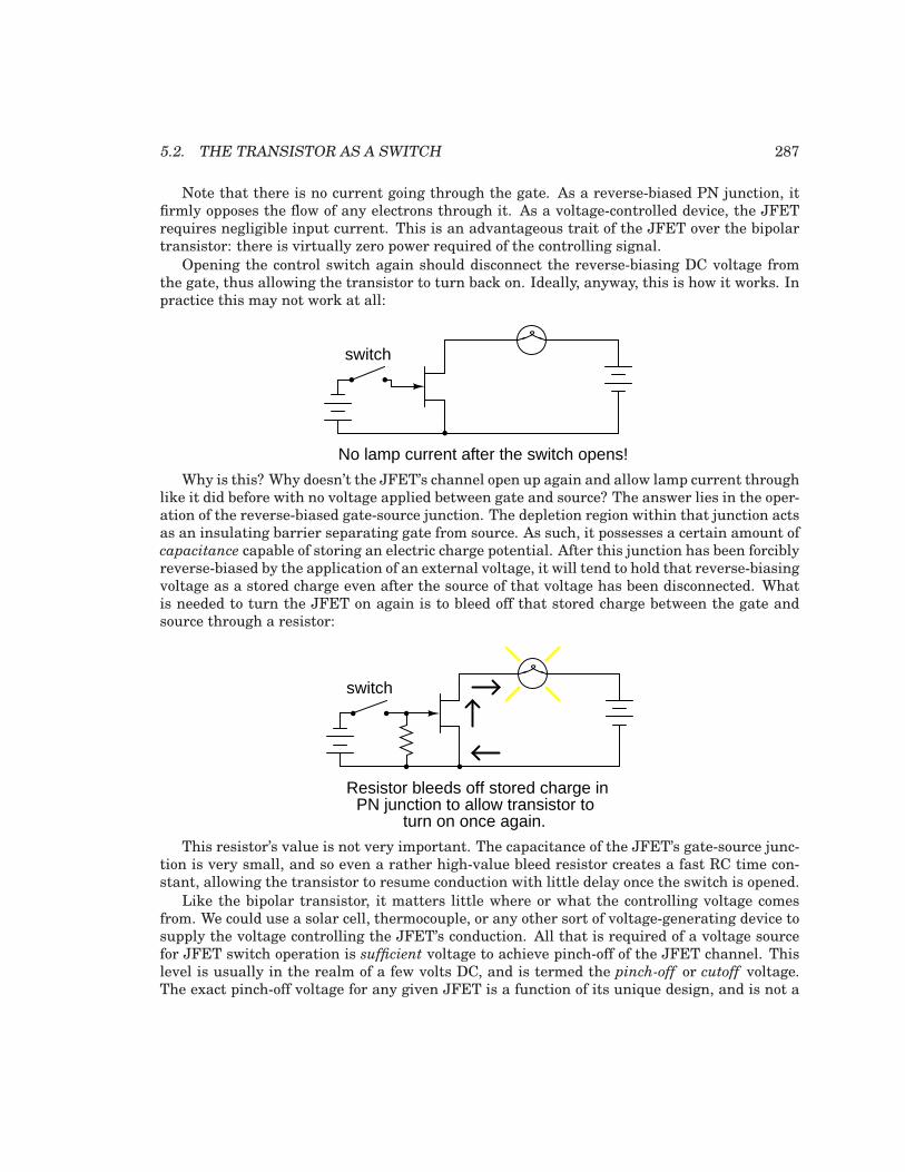
5.2. THE TRANSISTOR AS A SWITCH 287
Note that there is no current going through the gate. As a reverse-biased PN junction, itfirmly opposes the flow of any electrons through it. As a voltage-controlled device, the JFETrequires negligible input current. This is an advantageous trait of the JFET over the bipolartransistor: there is virtually zero power required of the controlling signal.
Opening the control switch again should disconnect the reverse-biasing DC voltage fromthe gate, thus allowing the transistor to turn back on. Ideally, anyway, this is how it works. Inpractice this may not work at all:
switch
No lamp current after the switch opens!
Why is this? Why doesn’t the JFET’s channel open up again and allow lamp current throughlike it did before with no voltage applied between gate and source? The answer lies in the oper-ation of the reverse-biased gate-source junction. The depletion region within that junction actsas an insulating barrier separating gate from source. As such, it possesses a certain amount ofcapacitance capable of storing an electric charge potential. After this junction has been forciblyreverse-biased by the application of an external voltage, it will tend to hold that reverse-biasingvoltage as a stored charge even after the source of that voltage has been disconnected. Whatis needed to turn the JFET on again is to bleed off that stored charge between the gate andsource through a resistor:
switch
Resistor bleeds off stored charge inPN junction to allow transistor to
turn on once again.
This resistor’s value is not very important. The capacitance of the JFET’s gate-source junc-tion is very small, and so even a rather high-value bleed resistor creates a fast RC time con-stant, allowing the transistor to resume conduction with little delay once the switch is opened.
Like the bipolar transistor, it matters little where or what the controlling voltage comesfrom. We could use a solar cell, thermocouple, or any other sort of voltage-generating device tosupply the voltage controlling the JFET’s conduction. All that is required of a voltage sourcefor JFET switch operation is sufficient voltage to achieve pinch-off of the JFET channel. Thislevel is usually in the realm of a few volts DC, and is termed the pinch-off or cutoff voltage.The exact pinch-off voltage for any given JFET is a function of its unique design, and is not a
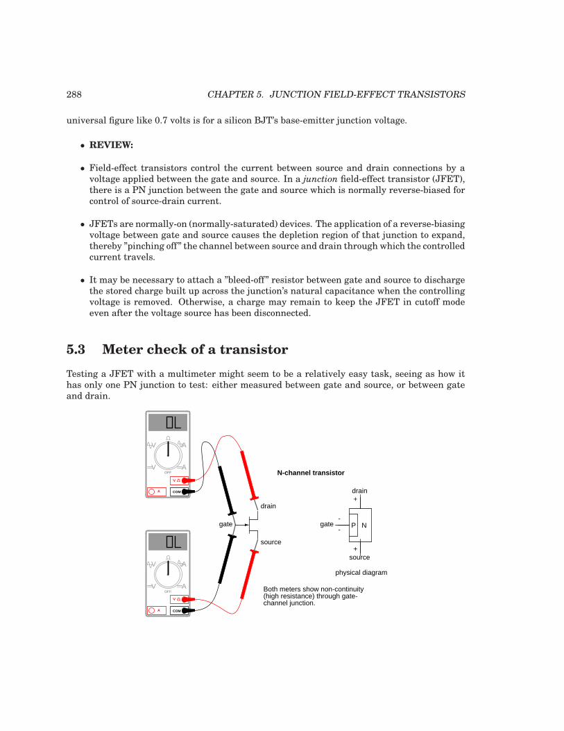
288 CHAPTER 5. JUNCTION FIELD-EFFECT TRANSISTORS
universal figure like 0.7 volts is for a silicon BJT’s base-emitter junction voltage.
• REVIEW:
• Field-effect transistors control the current between source and drain connections by avoltage applied between the gate and source. In a junction field-effect transistor (JFET),there is a PN junction between the gate and source which is normally reverse-biased forcontrol of source-drain current.
• JFETs are normally-on (normally-saturated) devices. The application of a reverse-biasingvoltage between gate and source causes the depletion region of that junction to expand,thereby ”pinching off” the channel between source and drain through which the controlledcurrent travels.
• It may be necessary to attach a ”bleed-off” resistor between gate and source to dischargethe stored charge built up across the junction’s natural capacitance when the controllingvoltage is removed. Otherwise, a charge may remain to keep the JFET in cutoff modeeven after the voltage source has been disconnected.
5.3 Meter check of a transistor
Testing a JFET with a multimeter might seem to be a relatively easy task, seeing as how ithas only one PN junction to test: either measured between gate and source, or between gateand drain.
COMA
V
V A
AOFF
COMA
V
V A
AOFF
+
-
+
-
N-channel transistor
gate
drain
source
physical diagram
P Ngate
drain
source
Both meters show non-continuity(high resistance) through gate-channel junction.
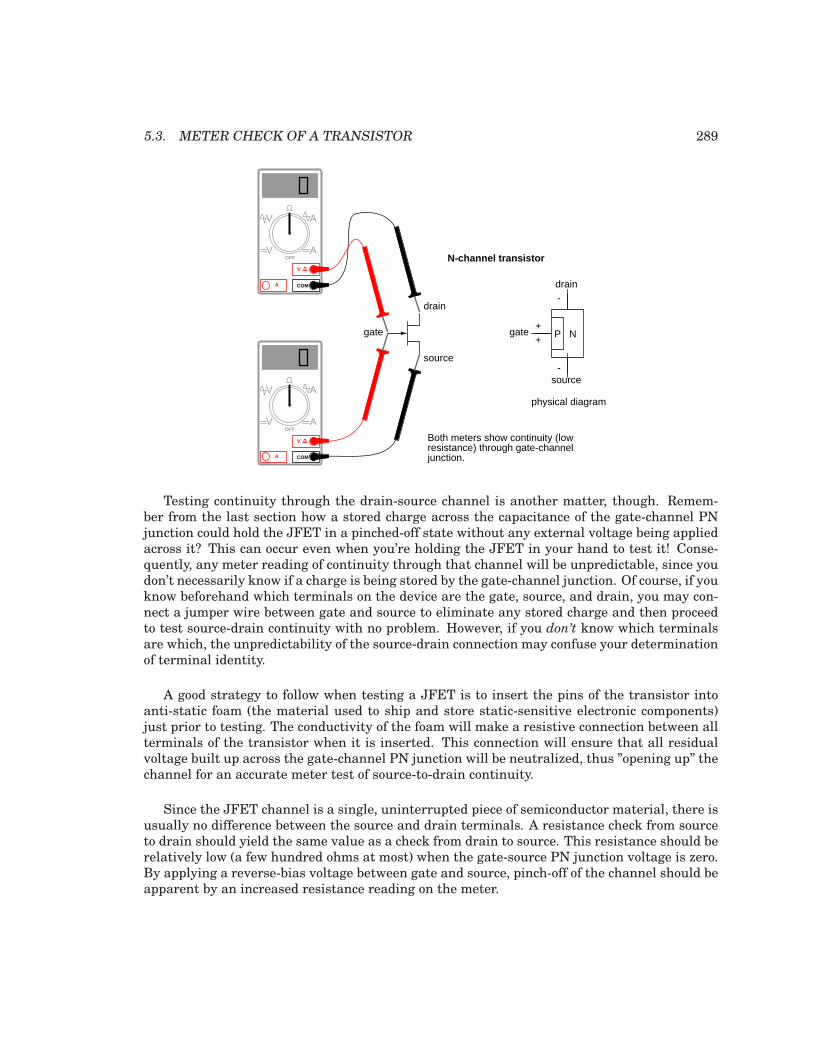
5.3. METER CHECK OF A TRANSISTOR 289
COMA
V
V A
AOFF
COMA
V
V A
AOFF
+
-
+
-
N-channel transistor
gate
drain
source
physical diagram
P Ngate
drain
source
Both meters show continuity (lowresistance) through gate-channeljunction.
Testing continuity through the drain-source channel is another matter, though. Remem-ber from the last section how a stored charge across the capacitance of the gate-channel PNjunction could hold the JFET in a pinched-off state without any external voltage being appliedacross it? This can occur even when you’re holding the JFET in your hand to test it! Conse-quently, any meter reading of continuity through that channel will be unpredictable, since youdon’t necessarily know if a charge is being stored by the gate-channel junction. Of course, if youknow beforehand which terminals on the device are the gate, source, and drain, you may con-nect a jumper wire between gate and source to eliminate any stored charge and then proceedto test source-drain continuity with no problem. However, if you don’t know which terminalsare which, the unpredictability of the source-drain connection may confuse your determinationof terminal identity.
A good strategy to follow when testing a JFET is to insert the pins of the transistor intoanti-static foam (the material used to ship and store static-sensitive electronic components)just prior to testing. The conductivity of the foam will make a resistive connection between allterminals of the transistor when it is inserted. This connection will ensure that all residualvoltage built up across the gate-channel PN junction will be neutralized, thus ”opening up” thechannel for an accurate meter test of source-to-drain continuity.
Since the JFET channel is a single, uninterrupted piece of semiconductor material, there isusually no difference between the source and drain terminals. A resistance check from sourceto drain should yield the same value as a check from drain to source. This resistance should berelatively low (a few hundred ohms at most) when the gate-source PN junction voltage is zero.By applying a reverse-bias voltage between gate and source, pinch-off of the channel should beapparent by an increased resistance reading on the meter.
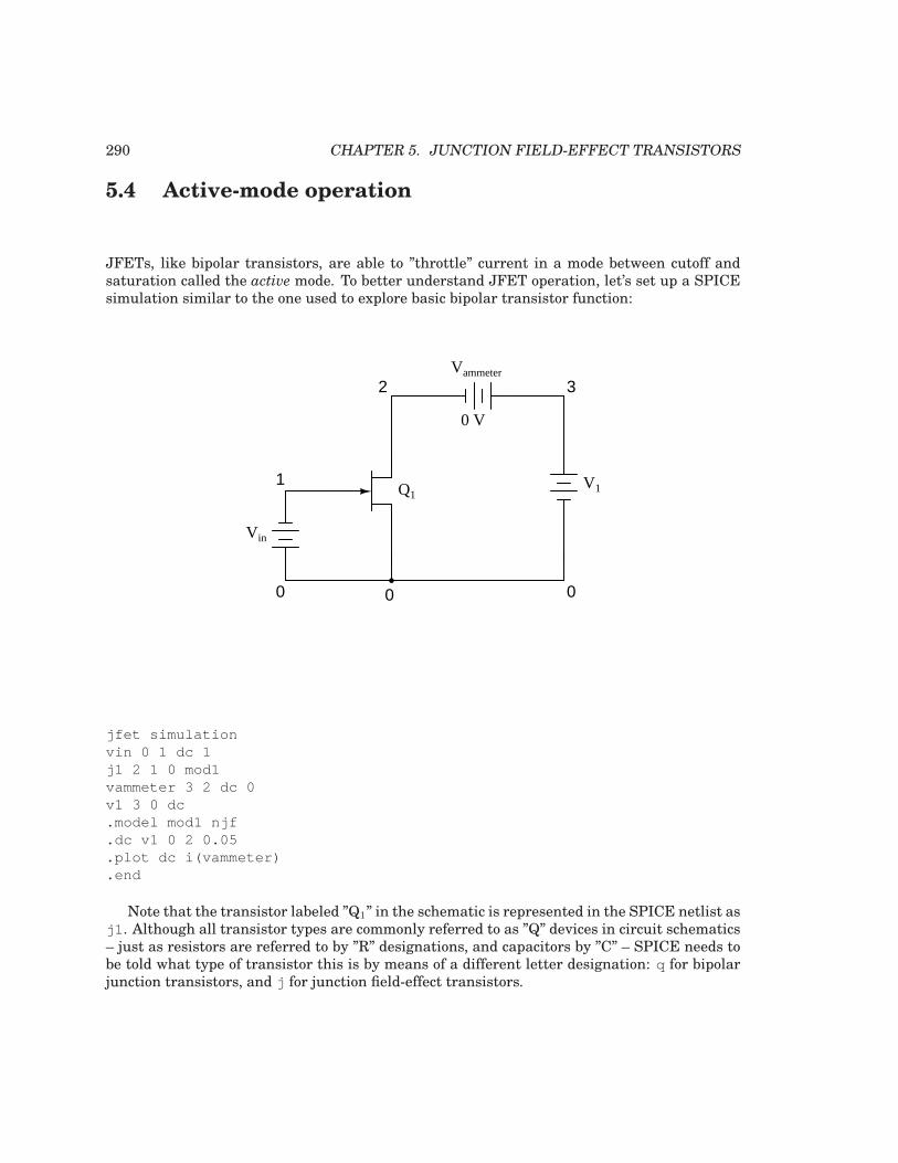
290 CHAPTER 5. JUNCTION FIELD-EFFECT TRANSISTORS
5.4 Active-mode operation
JFETs, like bipolar transistors, are able to ”throttle” current in a mode between cutoff andsaturation called the active mode. To better understand JFET operation, let’s set up a SPICEsimulation similar to the one used to explore basic bipolar transistor function:
V1Q1
Vammeter
0 V
1
0 0 0
2 3
Vin
jfet simulationvin 0 1 dc 1j1 2 1 0 mod1vammeter 3 2 dc 0v1 3 0 dc.model mod1 njf.dc v1 0 2 0.05.plot dc i(vammeter).end
Note that the transistor labeled ”Q1” in the schematic is represented in the SPICE netlist asj1 . Although all transistor types are commonly referred to as ”Q” devices in circuit schematics– just as resistors are referred to by ”R” designations, and capacitors by ”C” – SPICE needs tobe told what type of transistor this is by means of a different letter designation: q for bipolarjunction transistors, and j for junction field-effect transistors.
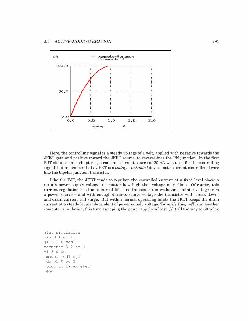
5.4. ACTIVE-MODE OPERATION 291
Here, the controlling signal is a steady voltage of 1 volt, applied with negative towards theJFET gate and positive toward the JFET source, to reverse-bias the PN junction. In the firstBJT simulation of chapter 4, a constant-current source of 20 µA was used for the controllingsignal, but remember that a JFET is a voltage-controlled device, not a current-controlled devicelike the bipolar junction transistor.
Like the BJT, the JFET tends to regulate the controlled current at a fixed level above acertain power supply voltage, no matter how high that voltage may climb. Of course, thiscurrent regulation has limits in real life – no transistor can withstand infinite voltage froma power source – and with enough drain-to-source voltage the transistor will ”break down”and drain current will surge. But within normal operating limits the JFET keeps the draincurrent at a steady level independent of power supply voltage. To verify this, we’ll run anothercomputer simulation, this time sweeping the power supply voltage (V1) all the way to 50 volts:
jfet simulationvin 0 1 dc 1j1 2 1 0 mod1vammeter 3 2 dc 0v1 3 0 dc.model mod1 njf.dc v1 0 50 2.plot dc i(vammeter).end
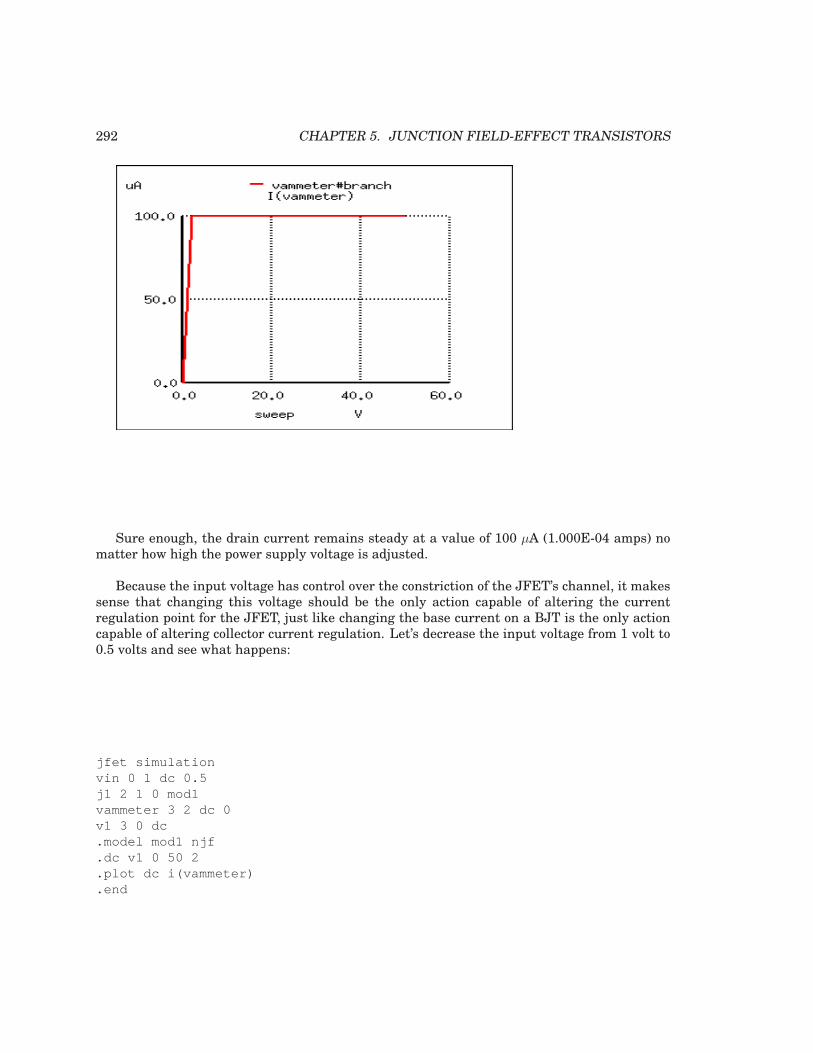
292 CHAPTER 5. JUNCTION FIELD-EFFECT TRANSISTORS
Sure enough, the drain current remains steady at a value of 100 µA (1.000E-04 amps) nomatter how high the power supply voltage is adjusted.
Because the input voltage has control over the constriction of the JFET’s channel, it makessense that changing this voltage should be the only action capable of altering the currentregulation point for the JFET, just like changing the base current on a BJT is the only actioncapable of altering collector current regulation. Let’s decrease the input voltage from 1 volt to0.5 volts and see what happens:
jfet simulationvin 0 1 dc 0.5j1 2 1 0 mod1vammeter 3 2 dc 0v1 3 0 dc.model mod1 njf.dc v1 0 50 2.plot dc i(vammeter).end
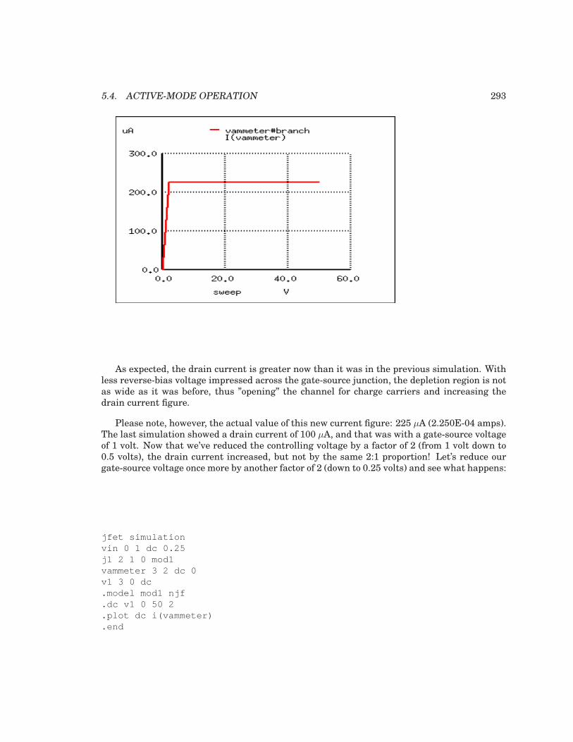
5.4. ACTIVE-MODE OPERATION 293
As expected, the drain current is greater now than it was in the previous simulation. Withless reverse-bias voltage impressed across the gate-source junction, the depletion region is notas wide as it was before, thus ”opening” the channel for charge carriers and increasing thedrain current figure.
Please note, however, the actual value of this new current figure: 225 µA (2.250E-04 amps).The last simulation showed a drain current of 100 µA, and that was with a gate-source voltageof 1 volt. Now that we’ve reduced the controlling voltage by a factor of 2 (from 1 volt down to0.5 volts), the drain current increased, but not by the same 2:1 proportion! Let’s reduce ourgate-source voltage once more by another factor of 2 (down to 0.25 volts) and see what happens:
jfet simulationvin 0 1 dc 0.25j1 2 1 0 mod1vammeter 3 2 dc 0v1 3 0 dc.model mod1 njf.dc v1 0 50 2.plot dc i(vammeter).end
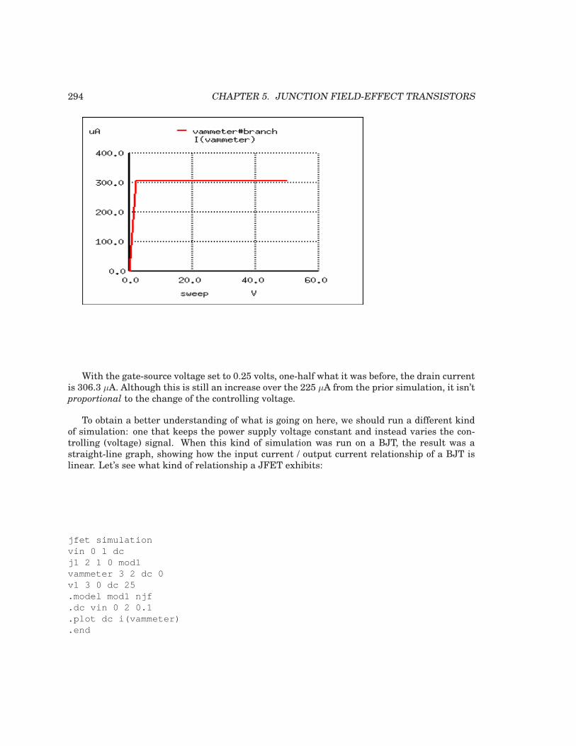
294 CHAPTER 5. JUNCTION FIELD-EFFECT TRANSISTORS
With the gate-source voltage set to 0.25 volts, one-half what it was before, the drain currentis 306.3 µA. Although this is still an increase over the 225 µA from the prior simulation, it isn’tproportional to the change of the controlling voltage.
To obtain a better understanding of what is going on here, we should run a different kindof simulation: one that keeps the power supply voltage constant and instead varies the con-trolling (voltage) signal. When this kind of simulation was run on a BJT, the result was astraight-line graph, showing how the input current / output current relationship of a BJT islinear. Let’s see what kind of relationship a JFET exhibits:
jfet simulationvin 0 1 dcj1 2 1 0 mod1vammeter 3 2 dc 0v1 3 0 dc 25.model mod1 njf.dc vin 0 2 0.1.plot dc i(vammeter).end
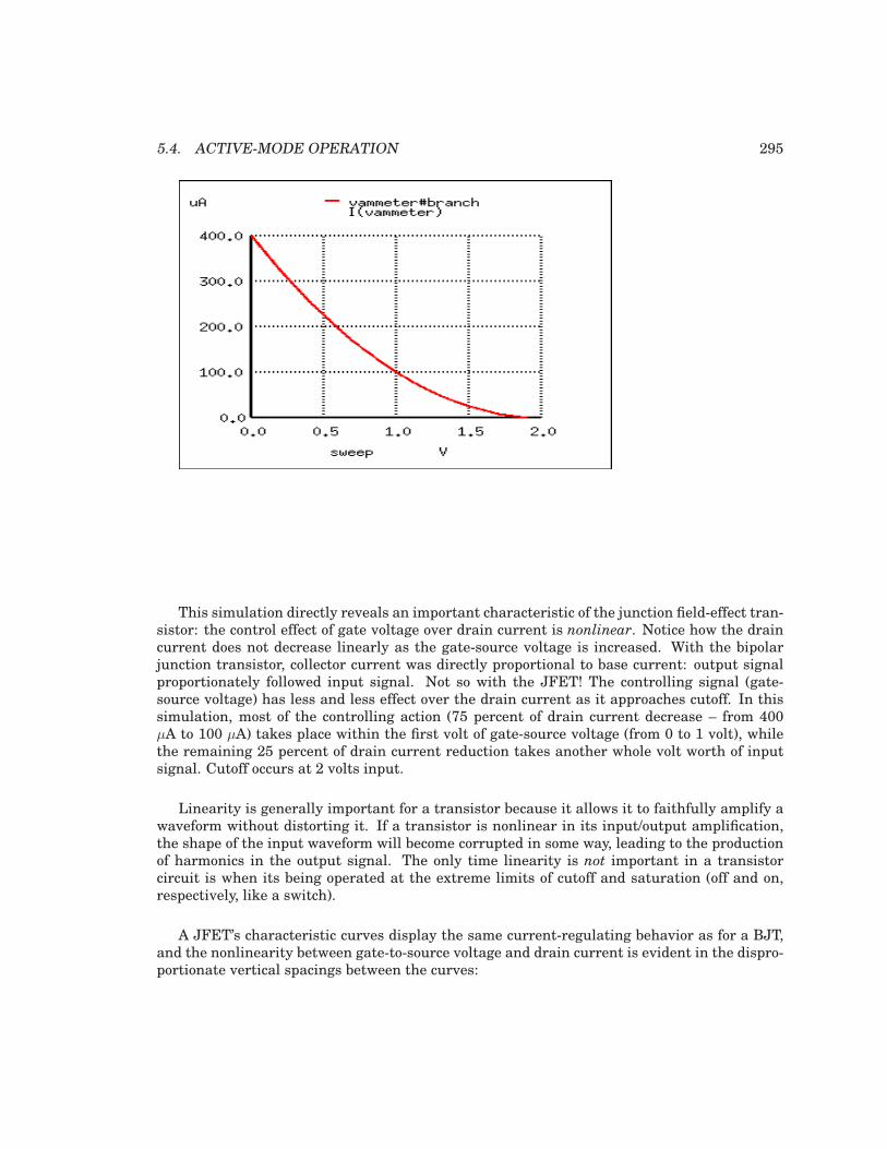
5.4. ACTIVE-MODE OPERATION 295
This simulation directly reveals an important characteristic of the junction field-effect tran-sistor: the control effect of gate voltage over drain current is nonlinear. Notice how the draincurrent does not decrease linearly as the gate-source voltage is increased. With the bipolarjunction transistor, collector current was directly proportional to base current: output signalproportionately followed input signal. Not so with the JFET! The controlling signal (gate-source voltage) has less and less effect over the drain current as it approaches cutoff. In thissimulation, most of the controlling action (75 percent of drain current decrease – from 400µA to 100 µA) takes place within the first volt of gate-source voltage (from 0 to 1 volt), whilethe remaining 25 percent of drain current reduction takes another whole volt worth of inputsignal. Cutoff occurs at 2 volts input.
Linearity is generally important for a transistor because it allows it to faithfully amplify awaveform without distorting it. If a transistor is nonlinear in its input/output amplification,the shape of the input waveform will become corrupted in some way, leading to the productionof harmonics in the output signal. The only time linearity is not important in a transistorcircuit is when its being operated at the extreme limits of cutoff and saturation (off and on,respectively, like a switch).
A JFET’s characteristic curves display the same current-regulating behavior as for a BJT,and the nonlinearity between gate-to-source voltage and drain current is evident in the dispro-portionate vertical spacings between the curves:
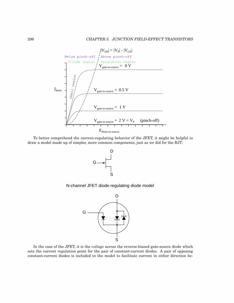
296 CHAPTER 5. JUNCTION FIELD-EFFECT TRANSISTORS
Idrain
Edrain-to-source
Vgate-to-source =
Vgate-to-source =
Vgate-to-source =
0 V
1 V
2 V = VP (pinch-off)
Vgate-to-source = 0.5 V
|VDS| = |VP| - |VGS|
Above pinch-offBelow pinch-off
Saturation region
Ohm
ic r
egio
n
Triode region
To better comprehend the current-regulating behavior of the JFET, it might be helpful todraw a model made up of simpler, more common components, just as we did for the BJT:
G
S
D
N-channel JFET diode-regulating diode model
S
D
G
In the case of the JFET, it is the voltage across the reverse-biased gate-source diode whichsets the current regulation point for the pair of constant-current diodes. A pair of opposingconstant-current diodes is included in the model to facilitate current in either direction be-
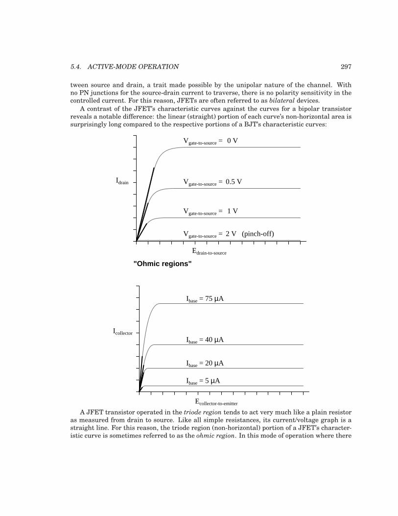
5.4. ACTIVE-MODE OPERATION 297
tween source and drain, a trait made possible by the unipolar nature of the channel. Withno PN junctions for the source-drain current to traverse, there is no polarity sensitivity in thecontrolled current. For this reason, JFETs are often referred to as bilateral devices.
A contrast of the JFET’s characteristic curves against the curves for a bipolar transistorreveals a notable difference: the linear (straight) portion of each curve’s non-horizontal area issurprisingly long compared to the respective portions of a BJT’s characteristic curves:
Idrain
Edrain-to-source
Vgate-to-source =
Vgate-to-source =
Vgate-to-source =
0 V
1 V
2 V (pinch-off)
Vgate-to-source = 0.5 V
"Ohmic regions"
Icollector
Ecollector-to-emitter
Ibase = 75 µA
Ibase = 40 µA
Ibase = 20 µA
Ibase = 5 µA
A JFET transistor operated in the triode region tends to act very much like a plain resistoras measured from drain to source. Like all simple resistances, its current/voltage graph is astraight line. For this reason, the triode region (non-horizontal) portion of a JFET’s character-istic curve is sometimes referred to as the ohmic region. In this mode of operation where there
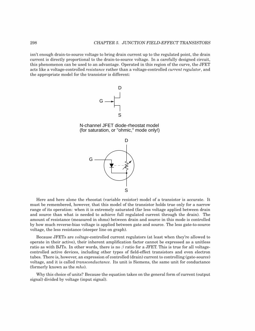
298 CHAPTER 5. JUNCTION FIELD-EFFECT TRANSISTORS
isn’t enough drain-to-source voltage to bring drain current up to the regulated point, the draincurrent is directly proportional to the drain-to-source voltage. In a carefully designed circuit,this phenomenon can be used to an advantage. Operated in this region of the curve, the JFETacts like a voltage-controlled resistance rather than a voltage-controlled current regulator, andthe appropriate model for the transistor is different:
N-channel JFET diode-rheostat model(for saturation, or "ohmic," mode only!)
G
D
S
S
D
G
Here and here alone the rheostat (variable resistor) model of a transistor is accurate. Itmust be remembered, however, that this model of the transistor holds true only for a narrowrange of its operation: when it is extremely saturated (far less voltage applied between drainand source than what is needed to achieve full regulated current through the drain). Theamount of resistance (measured in ohms) between drain and source in this mode is controlledby how much reverse-bias voltage is applied between gate and source. The less gate-to-sourcevoltage, the less resistance (steeper line on graph).
Because JFETs are voltage-controlled current regulators (at least when they’re allowed tooperate in their active), their inherent amplification factor cannot be expressed as a unitlessratio as with BJTs. In other words, there is no β ratio for a JFET. This is true for all voltage-controlled active devices, including other types of field-effect transistors and even electrontubes. There is, however, an expression of controlled (drain) current to controlling (gate-source)voltage, and it is called transconductance. Its unit is Siemens, the same unit for conductance(formerly known as the mho).
Why this choice of units? Because the equation takes on the general form of current (outputsignal) divided by voltage (input signal).
5.5. THE COMMON-SOURCE AMPLIFIER – PENDING 299
Where,
gfs = Transconductance in Siemens
gfs =∆ID
∆VGS
∆ID = Change in drain current∆VGS = Change in gate-source voltage
Unfortunately, the transconductance value for any JFET is not a stable quantity: it variessignificantly with the amount of gate-to-source control voltage applied to the transistor. As wesaw in the SPICE simulations, the drain current does not change proportionally with changesin gate-source voltage. To calculate drain current for any given gate-source voltage, there isanother equation that may be used. It is obviously nonlinear upon inspection (note the powerof 2), reflecting the nonlinear behavior we’ve already experienced in simulation:
ID = IDSS ( 1 - VGS
VGS(cutoff)
)2
Where,
ID = Drain current
IDSS = Drain current with gate shorted to source
VGS = Gate-to-source voltage
VGS(cutoff) = Pinch-off gate-to-source voltage
• REVIEW:
• In their active modes, JFETs regulate drain current according to the amount of reverse-bias voltage applied between gate and source, much like a BJT regulates collector currentaccording to base current. The mathematical ratio between drain current (output) andgate-to-source voltage (input) is called transconductance, and it is measured in units ofSiemens.
• The relationship between gate-source (control) voltage and drain (controlled) current isnonlinear: as gate-source voltage is decreased, drain current increases exponentially.That is to say, the transconductance of a JFET is not constant over its range of operation.
• In their triode region, JFETs regulate drain-to-source resistance according to the amountof reverse-bias voltage applied between gate and source. In other words, they act likevoltage-controlled resistances.
5.5 The common-source amplifier – PENDING
*** PENDING ***
300 CHAPTER 5. JUNCTION FIELD-EFFECT TRANSISTORS
• REVIEW:
•
•
•
5.6 The common-drain amplifier – PENDING
*** PENDING ***
• REVIEW:
•
•
•
5.7 The common-gate amplifier – PENDING
*** PENDING ***
• REVIEW:
•
•
•
5.8 Biasing techniques – PENDING
*** PENDING ***
• REVIEW:
•
•
•
5.9. TRANSISTOR RATINGS AND PACKAGES – PENDING 301
5.9 Transistor ratings and packages – PENDING
*** PENDING ***
• REVIEW:
•
•
•
5.10 JFET quirks – PENDING
*** PENDING ***
• REVIEW:
•
•
•

302 CHAPTER 5. JUNCTION FIELD-EFFECT TRANSISTORS
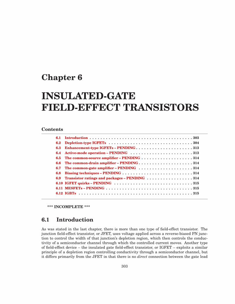
Chapter 6
INSULATED-GATE
FIELD-EFFECT TRANSISTORS
Contents
6.1 Introduction . . . . . . . . . . . . . . . . . . . . . . . . . . . . . . . . . . . . . . 303
6.2 Depletion-type IGFETs . . . . . . . . . . . . . . . . . . . . . . . . . . . . . . . 304
6.3 Enhancement-type IGFETs – PENDING . . . . . . . . . . . . . . . . . . . . . 313
6.4 Active-mode operation – PENDING . . . . . . . . . . . . . . . . . . . . . . . 313
6.5 The common-source amplifier – PENDING . . . . . . . . . . . . . . . . . . . 314
6.6 The common-drain amplifier – PENDING . . . . . . . . . . . . . . . . . . . . 314
6.7 The common-gate amplifier – PENDING . . . . . . . . . . . . . . . . . . . . 314
6.8 Biasing techniques – PENDING . . . . . . . . . . . . . . . . . . . . . . . . . . 314
6.9 Transistor ratings and packages – PENDING . . . . . . . . . . . . . . . . . 314
6.10 IGFET quirks – PENDING . . . . . . . . . . . . . . . . . . . . . . . . . . . . . 315
6.11 MESFETs – PENDING . . . . . . . . . . . . . . . . . . . . . . . . . . . . . . . . 315
6.12 IGBTs . . . . . . . . . . . . . . . . . . . . . . . . . . . . . . . . . . . . . . . . . . 315
*** INCOMPLETE ***
6.1 Introduction
As was stated in the last chapter, there is more than one type of field-effect transistor. Thejunction field-effect transistor, or JFET, uses voltage applied across a reverse-biased PN junc-tion to control the width of that junction’s depletion region, which then controls the conduc-tivity of a semiconductor channel through which the controlled current moves. Another typeof field-effect device – the insulated gate field-effect transistor, or IGFET – exploits a similarprinciple of a depletion region controlling conductivity through a semiconductor channel, butit differs primarily from the JFET in that there is no direct connection between the gate lead
303
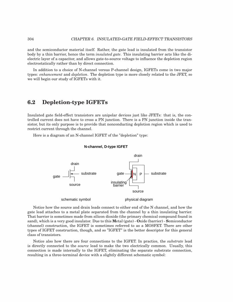
304 CHAPTER 6. INSULATED-GATE FIELD-EFFECT TRANSISTORS
and the semiconductor material itself. Rather, the gate lead is insulated from the transistorbody by a thin barrier, hence the term insulated gate. This insulating barrier acts like the di-electric layer of a capacitor, and allows gate-to-source voltage to influence the depletion regionelectrostatically rather than by direct connection.
In addition to a choice of N-channel versus P-channel design, IGFETs come in two majortypes: enhancement and depletion. The depletion type is more closely related to the JFET, sowe will begin our study of IGFETs with it.
6.2 Depletion-type IGFETs
Insulated gate field-effect transistors are unipolar devices just like JFETs: that is, the con-trolled current does not have to cross a PN junction. There is a PN junction inside the tran-sistor, but its only purpose is to provide that nonconducting depletion region which is used torestrict current through the channel.
Here is a diagram of an N-channel IGFET of the ”depletion” type:
schematic symbol physical diagram
PNgate
drain
source
drain
source
gatesubstrate
N-channel, D-type IGFET
insulatingbarrier
substrate
Notice how the source and drain leads connect to either end of the N channel, and how thegate lead attaches to a metal plate separated from the channel by a thin insulating barrier.That barrier is sometimes made from silicon dioxide (the primary chemical compound found insand), which is a very good insulator. Due to thisMetal (gate) -Oxide (barrier) - Semiconductor(channel) construction, the IGFET is sometimes referred to as a MOSFET. There are othertypes of IGFET construction, though, and so ”IGFET” is the better descriptor for this generalclass of transistors.
Notice also how there are four connections to the IGFET. In practice, the substrate leadis directly connected to the source lead to make the two electrically common. Usually, thisconnection is made internally to the IGFET, eliminating the separate substrate connection,resulting in a three-terminal device with a slightly different schematic symbol:
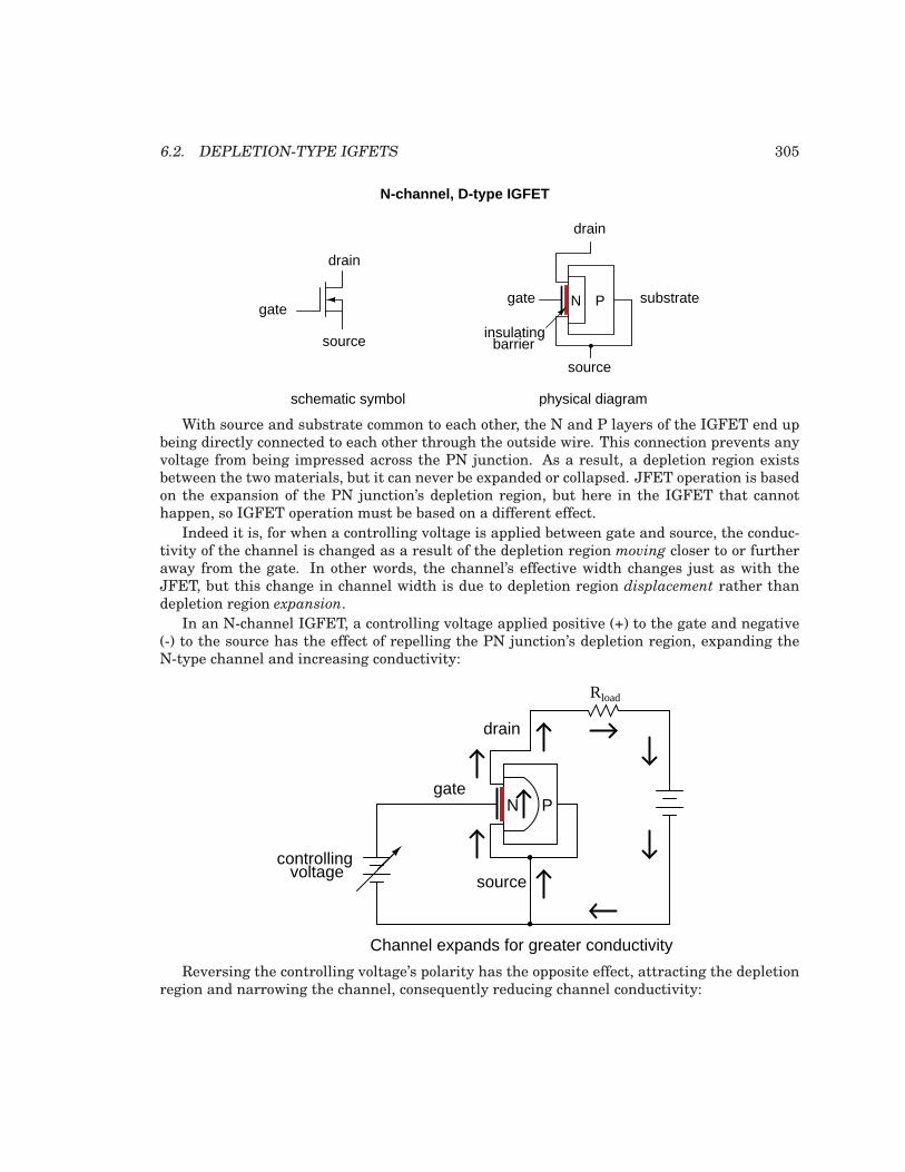
6.2. DEPLETION-TYPE IGFETS 305
schematic symbol physical diagram
PNgate
drain
source
drain
source
gate
N-channel, D-type IGFET
insulatingbarrier
substrate
With source and substrate common to each other, the N and P layers of the IGFET end upbeing directly connected to each other through the outside wire. This connection prevents anyvoltage from being impressed across the PN junction. As a result, a depletion region existsbetween the two materials, but it can never be expanded or collapsed. JFET operation is basedon the expansion of the PN junction’s depletion region, but here in the IGFET that cannothappen, so IGFET operation must be based on a different effect.
Indeed it is, for when a controlling voltage is applied between gate and source, the conduc-tivity of the channel is changed as a result of the depletion region moving closer to or furtheraway from the gate. In other words, the channel’s effective width changes just as with theJFET, but this change in channel width is due to depletion region displacement rather thandepletion region expansion.
In an N-channel IGFET, a controlling voltage applied positive (+) to the gate and negative(-) to the source has the effect of repelling the PN junction’s depletion region, expanding theN-type channel and increasing conductivity:
PNgate
drain
source
Rload
controllingvoltage
Channel expands for greater conductivity
Reversing the controlling voltage’s polarity has the opposite effect, attracting the depletionregion and narrowing the channel, consequently reducing channel conductivity:
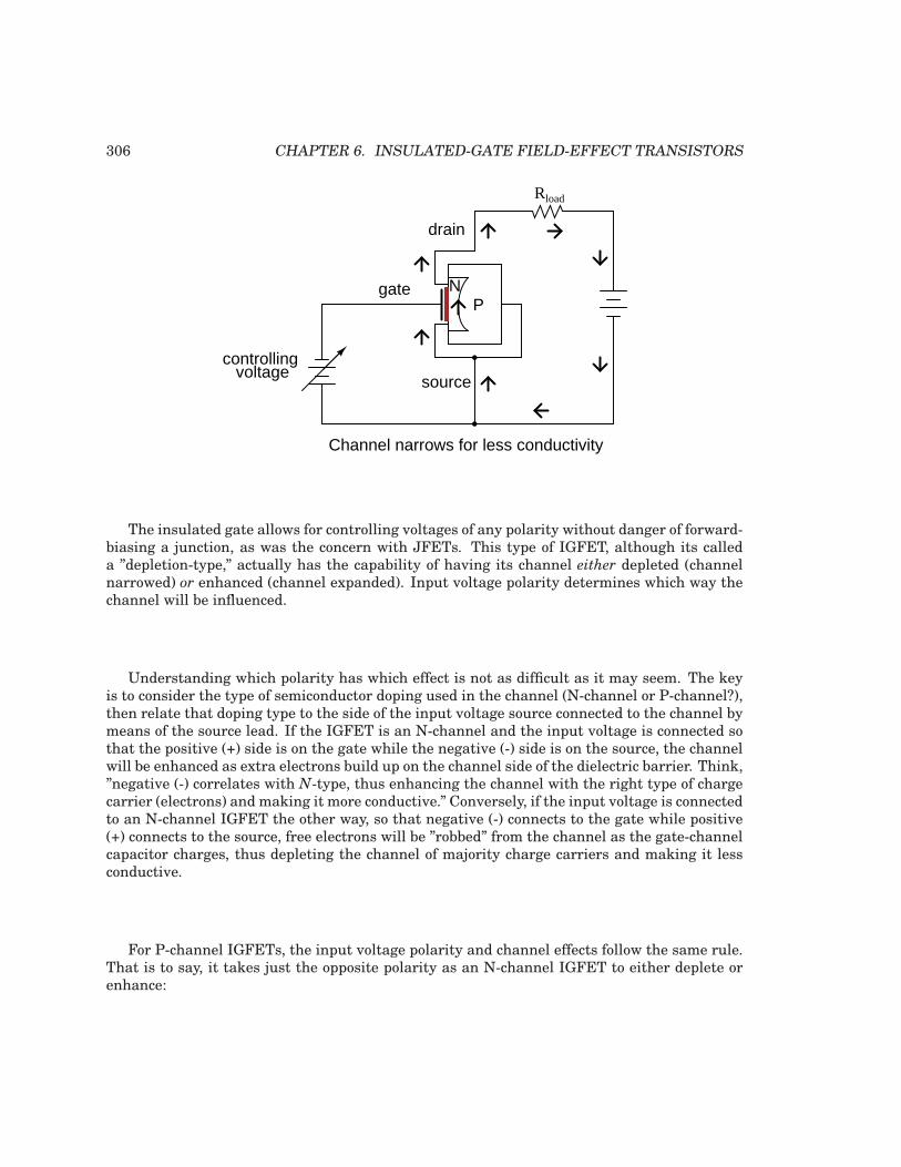
306 CHAPTER 6. INSULATED-GATE FIELD-EFFECT TRANSISTORS
PNgate
drain
source
Rload
controllingvoltage
Channel narrows for less conductivity
The insulated gate allows for controlling voltages of any polarity without danger of forward-biasing a junction, as was the concern with JFETs. This type of IGFET, although its calleda ”depletion-type,” actually has the capability of having its channel either depleted (channelnarrowed) or enhanced (channel expanded). Input voltage polarity determines which way thechannel will be influenced.
Understanding which polarity has which effect is not as difficult as it may seem. The keyis to consider the type of semiconductor doping used in the channel (N-channel or P-channel?),then relate that doping type to the side of the input voltage source connected to the channel bymeans of the source lead. If the IGFET is an N-channel and the input voltage is connected sothat the positive (+) side is on the gate while the negative (-) side is on the source, the channelwill be enhanced as extra electrons build up on the channel side of the dielectric barrier. Think,”negative (-) correlates with N-type, thus enhancing the channel with the right type of chargecarrier (electrons) and making it more conductive.” Conversely, if the input voltage is connectedto an N-channel IGFET the other way, so that negative (-) connects to the gate while positive(+) connects to the source, free electrons will be ”robbed” from the channel as the gate-channelcapacitor charges, thus depleting the channel of majority charge carriers and making it lessconductive.
For P-channel IGFETs, the input voltage polarity and channel effects follow the same rule.That is to say, it takes just the opposite polarity as an N-channel IGFET to either deplete orenhance:
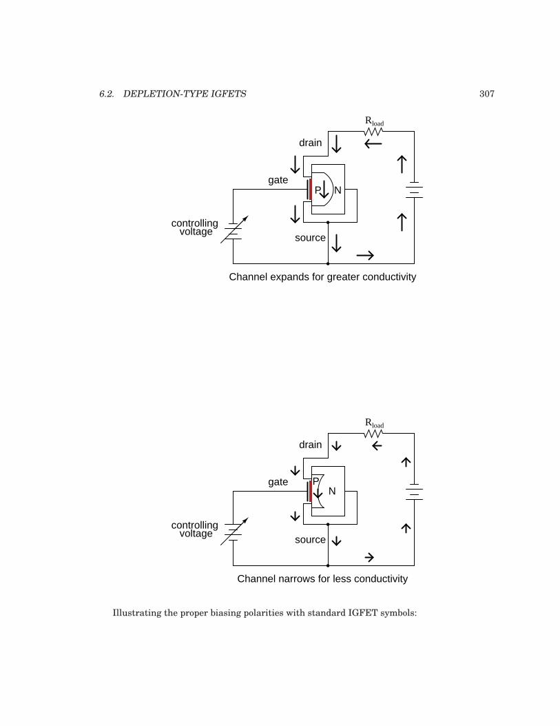
6.2. DEPLETION-TYPE IGFETS 307
P Ngate
drain
source
Rload
controllingvoltage
Channel expands for greater conductivity
PN
gate
drain
source
Rload
controllingvoltage
Channel narrows for less conductivity
Illustrating the proper biasing polarities with standard IGFET symbols:
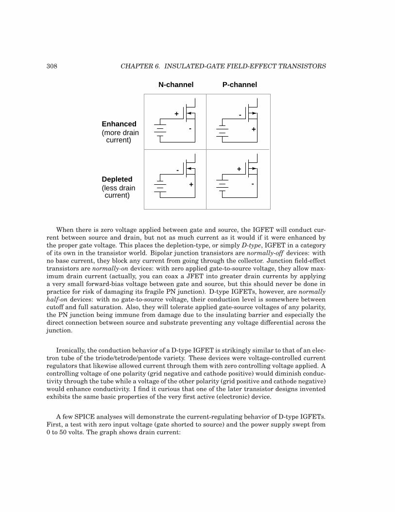
308 CHAPTER 6. INSULATED-GATE FIELD-EFFECT TRANSISTORS
N-channel P-channel
Enhanced(more drain
current)
Depleted(less draincurrent)
+
-
+
- +
-
+
-
When there is zero voltage applied between gate and source, the IGFET will conduct cur-rent between source and drain, but not as much current as it would if it were enhanced bythe proper gate voltage. This places the depletion-type, or simply D-type, IGFET in a categoryof its own in the transistor world. Bipolar junction transistors are normally-off devices: withno base current, they block any current from going through the collector. Junction field-effecttransistors are normally-on devices: with zero applied gate-to-source voltage, they allow max-imum drain current (actually, you can coax a JFET into greater drain currents by applyinga very small forward-bias voltage between gate and source, but this should never be done inpractice for risk of damaging its fragile PN junction). D-type IGFETs, however, are normally
half-on devices: with no gate-to-source voltage, their conduction level is somewhere betweencutoff and full saturation. Also, they will tolerate applied gate-source voltages of any polarity,the PN junction being immune from damage due to the insulating barrier and especially thedirect connection between source and substrate preventing any voltage differential across thejunction.
Ironically, the conduction behavior of a D-type IGFET is strikingly similar to that of an elec-tron tube of the triode/tetrode/pentode variety. These devices were voltage-controlled currentregulators that likewise allowed current through them with zero controlling voltage applied. Acontrolling voltage of one polarity (grid negative and cathode positive) would diminish conduc-tivity through the tube while a voltage of the other polarity (grid positive and cathode negative)would enhance conductivity. I find it curious that one of the later transistor designs inventedexhibits the same basic properties of the very first active (electronic) device.
A few SPICE analyses will demonstrate the current-regulating behavior of D-type IGFETs.First, a test with zero input voltage (gate shorted to source) and the power supply swept from0 to 50 volts. The graph shows drain current:
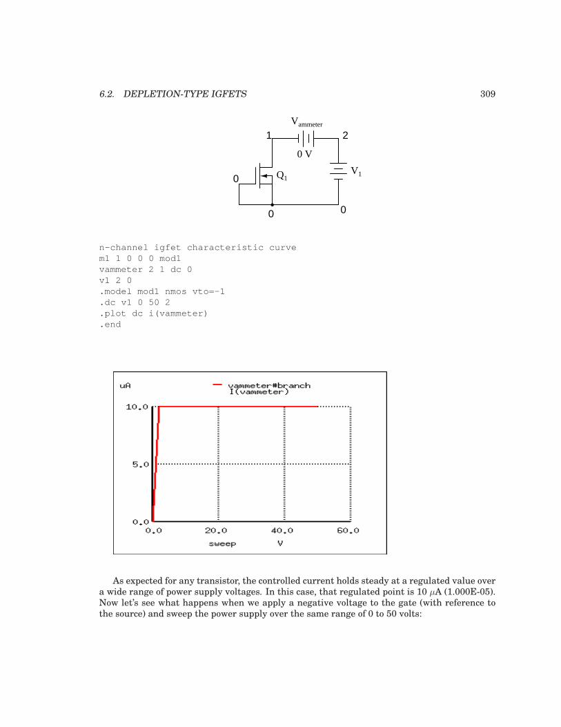
6.2. DEPLETION-TYPE IGFETS 309
Q1V1
Vammeter
0 V
0
0
0
1 2
n-channel igfet characteristic curvem1 1 0 0 0 mod1vammeter 2 1 dc 0v1 2 0.model mod1 nmos vto=-1.dc v1 0 50 2.plot dc i(vammeter).end
As expected for any transistor, the controlled current holds steady at a regulated value overa wide range of power supply voltages. In this case, that regulated point is 10 µA (1.000E-05).Now let’s see what happens when we apply a negative voltage to the gate (with reference tothe source) and sweep the power supply over the same range of 0 to 50 volts:
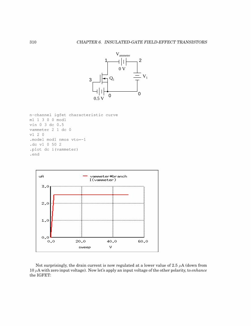
310 CHAPTER 6. INSULATED-GATE FIELD-EFFECT TRANSISTORS
Q1V1
Vammeter
0 V
0 0
1 2
3
0.5 V
n-channel igfet characteristic curvem1 1 3 0 0 mod1vin 0 3 dc 0.5vammeter 2 1 dc 0v1 2 0.model mod1 nmos vto=-1.dc v1 0 50 2.plot dc i(vammeter).end
Not surprisingly, the drain current is now regulated at a lower value of 2.5 µA (down from10 µAwith zero input voltage). Now let’s apply an input voltage of the other polarity, to enhancethe IGFET:
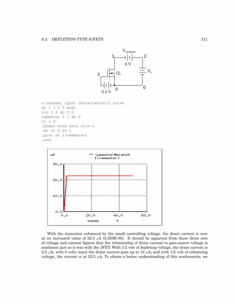
6.2. DEPLETION-TYPE IGFETS 311
Q1V1
Vammeter
0 V
0 0
1 2
3
0.5 V
n-channel igfet characteristic curvem1 1 3 0 0 mod1vin 3 0 dc 0.5vammeter 2 1 dc 0v1 2 0.model mod1 nmos vto=-1.dc v1 0 50 2.plot dc i(vammeter).end
With the transistor enhanced by the small controlling voltage, the drain current is nowat an increased value of 22.5 µA (2.250E-05). It should be apparent from these three setsof voltage and current figures that the relationship of drain current to gate-source voltage isnonlinear just as it was with the JFET. With 1/2 volt of depleting voltage, the drain current is2.5 µA; with 0 volts input the drain current goes up to 10 µA; and with 1/2 volt of enhancingvoltage, the current is at 22.5 µA. To obtain a better understanding of this nonlinearity, we
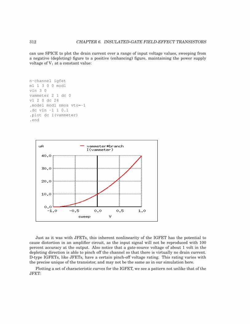
312 CHAPTER 6. INSULATED-GATE FIELD-EFFECT TRANSISTORS
can use SPICE to plot the drain current over a range of input voltage values, sweeping froma negative (depleting) figure to a positive (enhancing) figure, maintaining the power supplyvoltage of V1 at a constant value:
n-channel igfetm1 1 3 0 0 mod1vin 3 0vammeter 2 1 dc 0v1 2 0 dc 24.model mod1 nmos vto=-1.dc vin -1 1 0.1.plot dc i(vammeter).end
Just as it was with JFETs, this inherent nonlinearity of the IGFET has the potential tocause distortion in an amplifier circuit, as the input signal will not be reproduced with 100percent accuracy at the output. Also notice that a gate-source voltage of about 1 volt in thedepleting direction is able to pinch off the channel so that there is virtually no drain current.D-type IGFETs, like JFETs, have a certain pinch-off voltage rating. This rating varies withthe precise unique of the transistor, and may not be the same as in our simulation here.
Plotting a set of characteristic curves for the IGFET, we see a pattern not unlike that of theJFET:
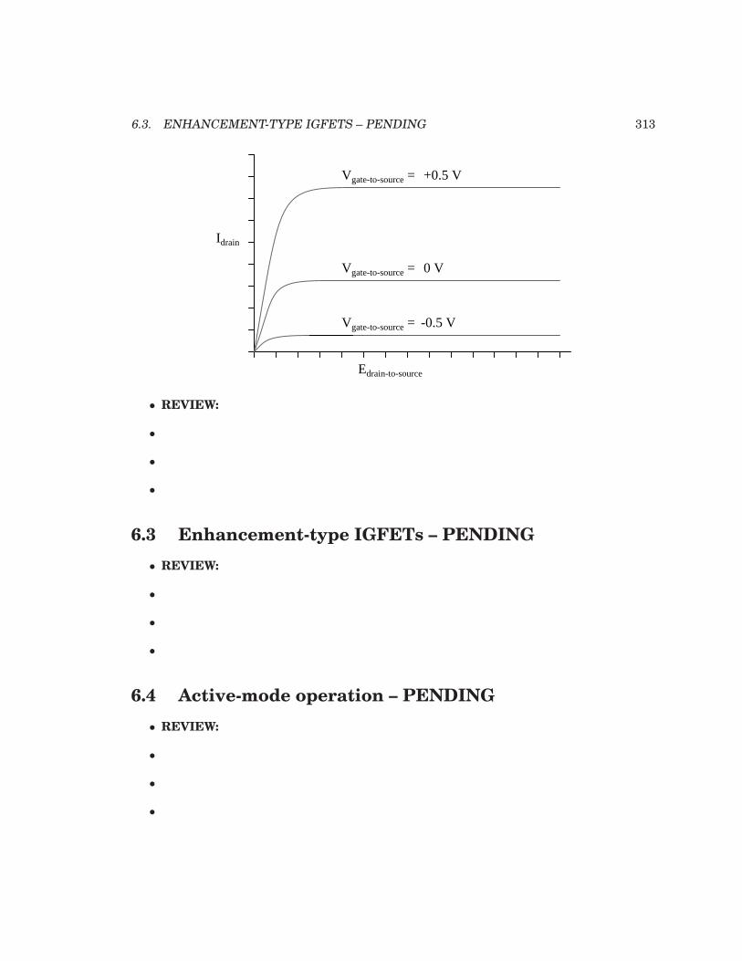
6.3. ENHANCEMENT-TYPE IGFETS – PENDING 313
Idrain
Edrain-to-source
Vgate-to-source =
Vgate-to-source =
0 VVgate-to-source =
-0.5 V
+0.5 V
• REVIEW:
•
•
•
6.3 Enhancement-type IGFETs – PENDING
• REVIEW:
•
•
•
6.4 Active-mode operation – PENDING
• REVIEW:
•
•
•
314 CHAPTER 6. INSULATED-GATE FIELD-EFFECT TRANSISTORS
6.5 The common-source amplifier – PENDING
• REVIEW:
•
•
•
6.6 The common-drain amplifier – PENDING
• REVIEW:
•
•
•
6.7 The common-gate amplifier – PENDING
• REVIEW:
•
•
•
6.8 Biasing techniques – PENDING
• REVIEW:
•
•
•
6.9 Transistor ratings and packages – PENDING
• REVIEW:
•
•
•
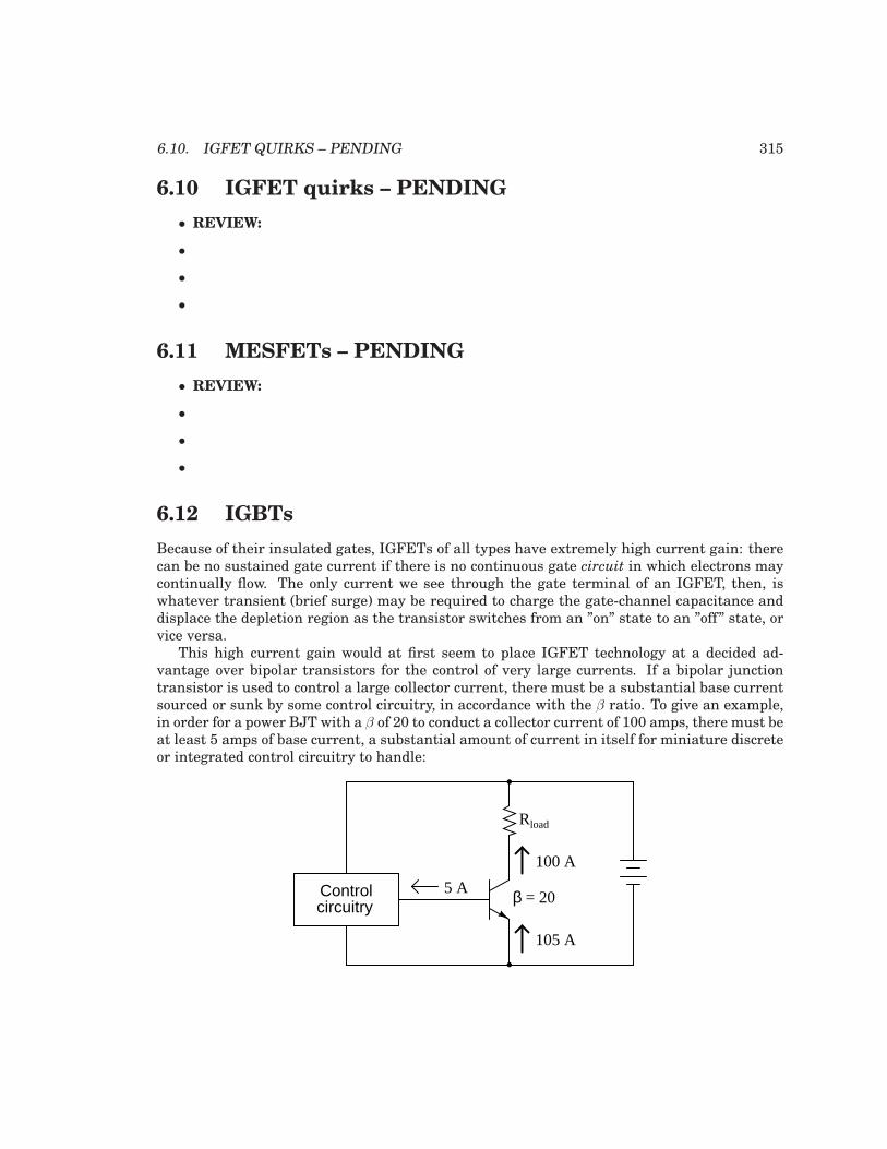
6.10. IGFET QUIRKS – PENDING 315
6.10 IGFET quirks – PENDING
• REVIEW:
•
•
•
6.11 MESFETs – PENDING
• REVIEW:
•
•
•
6.12 IGBTs
Because of their insulated gates, IGFETs of all types have extremely high current gain: therecan be no sustained gate current if there is no continuous gate circuit in which electrons maycontinually flow. The only current we see through the gate terminal of an IGFET, then, iswhatever transient (brief surge) may be required to charge the gate-channel capacitance anddisplace the depletion region as the transistor switches from an ”on” state to an ”off” state, orvice versa.
This high current gain would at first seem to place IGFET technology at a decided ad-vantage over bipolar transistors for the control of very large currents. If a bipolar junctiontransistor is used to control a large collector current, there must be a substantial base currentsourced or sunk by some control circuitry, in accordance with the β ratio. To give an example,in order for a power BJT with a β of 20 to conduct a collector current of 100 amps, there must beat least 5 amps of base current, a substantial amount of current in itself for miniature discreteor integrated control circuitry to handle:
β = 20
Rload
100 A
105 A
Controlcircuitry
5 A
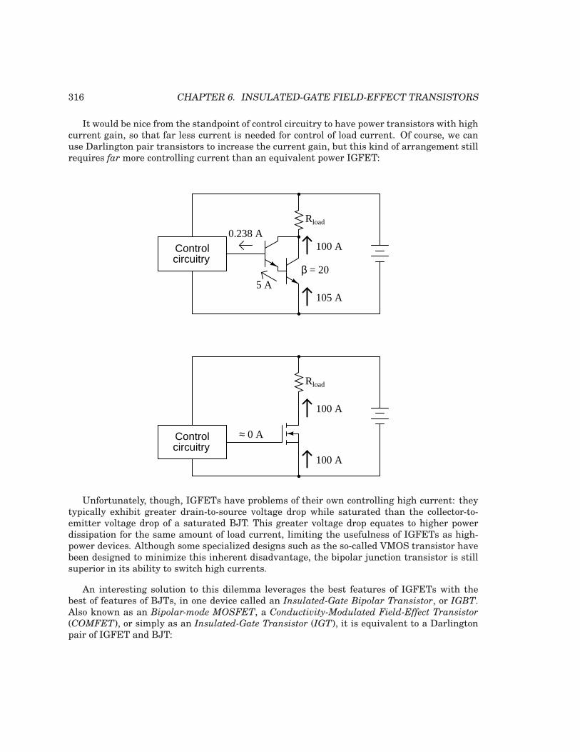
316 CHAPTER 6. INSULATED-GATE FIELD-EFFECT TRANSISTORS
It would be nice from the standpoint of control circuitry to have power transistors with highcurrent gain, so that far less current is needed for control of load current. Of course, we canuse Darlington pair transistors to increase the current gain, but this kind of arrangement stillrequires far more controlling current than an equivalent power IGFET:
β = 20
Rload
100 A
105 A
Controlcircuitry
5 A
0.238 A
Rload
100 A
Controlcircuitry
100 A
≈ 0 A
Unfortunately, though, IGFETs have problems of their own controlling high current: theytypically exhibit greater drain-to-source voltage drop while saturated than the collector-to-emitter voltage drop of a saturated BJT. This greater voltage drop equates to higher powerdissipation for the same amount of load current, limiting the usefulness of IGFETs as high-power devices. Although some specialized designs such as the so-called VMOS transistor havebeen designed to minimize this inherent disadvantage, the bipolar junction transistor is stillsuperior in its ability to switch high currents.
An interesting solution to this dilemma leverages the best features of IGFETs with thebest of features of BJTs, in one device called an Insulated-Gate Bipolar Transistor, or IGBT.Also known as an Bipolar-mode MOSFET, a Conductivity-Modulated Field-Effect Transistor
(COMFET), or simply as an Insulated-Gate Transistor (IGT), it is equivalent to a Darlingtonpair of IGFET and BJT:
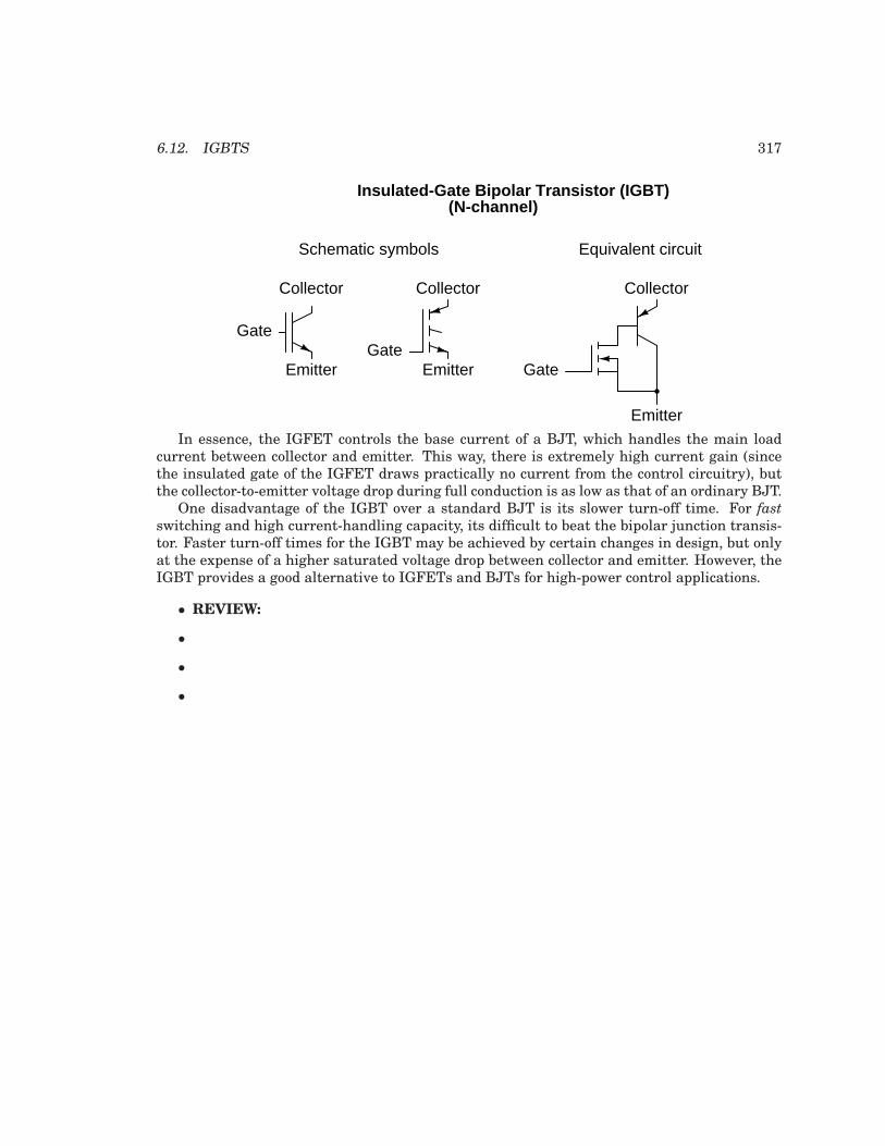
6.12. IGBTS 317
Insulated-Gate Bipolar Transistor (IGBT)
Schematic symbols Equivalent circuit
(N-channel)
Collector
Gate
Emitter
CollectorCollector
EmitterEmitterGate
Gate
In essence, the IGFET controls the base current of a BJT, which handles the main loadcurrent between collector and emitter. This way, there is extremely high current gain (sincethe insulated gate of the IGFET draws practically no current from the control circuitry), butthe collector-to-emitter voltage drop during full conduction is as low as that of an ordinary BJT.
One disadvantage of the IGBT over a standard BJT is its slower turn-off time. For fast
switching and high current-handling capacity, its difficult to beat the bipolar junction transis-tor. Faster turn-off times for the IGBT may be achieved by certain changes in design, but onlyat the expense of a higher saturated voltage drop between collector and emitter. However, theIGBT provides a good alternative to IGFETs and BJTs for high-power control applications.
• REVIEW:
•
•
•

318 CHAPTER 6. INSULATED-GATE FIELD-EFFECT TRANSISTORS
Chapter 7
THYRISTORS
Contents
7.1 Hysteresis . . . . . . . . . . . . . . . . . . . . . . . . . . . . . . . . . . . . . . . 319
7.2 Gas discharge tubes . . . . . . . . . . . . . . . . . . . . . . . . . . . . . . . . . 320
7.3 The Shockley Diode . . . . . . . . . . . . . . . . . . . . . . . . . . . . . . . . . 324
7.4 The DIAC . . . . . . . . . . . . . . . . . . . . . . . . . . . . . . . . . . . . . . . . 331
7.5 The Silicon-Controlled Rectifier (SCR) . . . . . . . . . . . . . . . . . . . . . 331
7.6 The TRIAC . . . . . . . . . . . . . . . . . . . . . . . . . . . . . . . . . . . . . . . 343
7.7 Optothyristors . . . . . . . . . . . . . . . . . . . . . . . . . . . . . . . . . . . . . 346
7.8 The Unijunction Transistor (UJT) . . . . . . . . . . . . . . . . . . . . . . . . 346
7.9 The Silicon-Controlled Switch (SCS) . . . . . . . . . . . . . . . . . . . . . . . 352
7.10 Field-effect-controlled thyristors . . . . . . . . . . . . . . . . . . . . . . . . . 354
Bibliography . . . . . . . . . . . . . . . . . . . . . . . . . . . . . . . . . . . . . . . . . 356
7.1 Hysteresis
Thyristors are a class of semiconductor components exhibiting hysteresis, that property wherebya system fails to return to its original state after some cause of state change has been removed.A very simple example of hysteresis is the mechanical action of a toggle switch: when thelever is pushed, it flips to one of two extreme states (positions) and will remain there evenafter the source of motion is removed (after you remove your hand from the switch lever). Toillustrate the absence of hysteresis, consider the action of a ”momentary” pushbutton switch,which returns to its original state after the button is no longer pressed: when the stimulus isremoved (your hand), the system (switch) immediately and fully returns to its prior state withno ”latching” behavior.
Bipolar, junction field-effect, and insulated gate field-effect transistors are all non-hystericdevices. That is, these do not inherently ”latch” into a state after being stimulated by a voltageor current signal. For any given input signal at any given time, a transistor will exhibit a
319
320 CHAPTER 7. THYRISTORS
predictable output response as defined by its characteristic curve. Thyristors, on the otherhand, are semiconductor devices that tend to stay ”on” once turned on, and tend to stay ”off”once turned off. A momentary event is able to flip these devices into either their on or offstates where these will remain that way on their own, even after the cause of the state changeis taken away. As such, these are useful only as on/off switching devices – much like a toggleswitch – and cannot be used as analog signal amplifiers.
Thyristors are constructed using the same technology as bipolar junction transistors, andin fact may be analyzed as circuits comprised of transistor pairs. How then, can a hysteric de-vice (a thyristor) be made from non-hysteric devices (transistors)? The answer to this questionis positive feedback, also known as regenerative feedback. As you should recall, feedback is thecondition where a percentage of the output signal is ”fed back” to the input of an amplifyingdevice. Negative, or degenerative, feedback results in a diminishing of voltage gain with in-creases in stability, linearity, and bandwidth. Positive feedback, on the other hand, results ina kind of instability where the amplifier’s output tends to ”saturate.” In the case of thyristors,this saturating tendency equates to the device ”wanting” to stay on once turned on, and offonce turned off.
In this chapter we will explore several different kinds of thyristors, most of which stem froma single, basic two-transistor core circuit. Before we do that, though, it would be beneficial tostudy the technological predecessor to thyristors: gas discharge tubes.
7.2 Gas discharge tubes
If you’ve ever witnessed a lightning storm, you’ve seen electrical hysteresis in action (andprobably didn’t realize what you were seeing). The action of strong wind and rain accumu-lates tremendous static electric charges between cloud and earth, and between clouds as well.Electric charge imbalances manifest themselves as high voltages, and when the electrical re-sistance of air can no longer hold these high voltages at bay, huge surges of current travelbetween opposing poles of electrical charge which we call ”lightning.”
The buildup of high voltages by wind and rain is a fairly continuous process, the rate ofcharge accumulation increasing under the proper atmospheric conditions. However, lightningbolts are anything but continuous: they exist as relatively brief surges rather than continuousdischarges. Why is this? Why don’t we see soft, glowing lightning arcs instead of violently brieflightning bolts? The answer lies in the nonlinear (and hysteric) resistance of air.
Under ordinary conditions, air has an extremely high amount of resistance. It is so high, infact, that we typically treat its resistance as infinite and electrical conduction through the airas negligible. The presence of water and dust in air lowers its resistance some, but it is still aninsulator for most practical purposes. When enough high voltage is applied across a distanceof air, though, its electrical properties change: electrons become ”stripped” from their normalpositions around their respective atoms and are liberated to constitute a current. In this state,air is considered to be ionized and is called a plasma rather than a gas. This usage of the word”plasma” is not to be confused with the medical term (meaning the fluid portion of blood), butis a fourth state of matter, the other three being solid, liquid, and vapor (gas). Plasma is arelatively good conductor of electricity, its specific resistance being much lower than that of thesame substance in its gaseous state.
As an electric current moves through the plasma, there is energy dissipated in the plasma
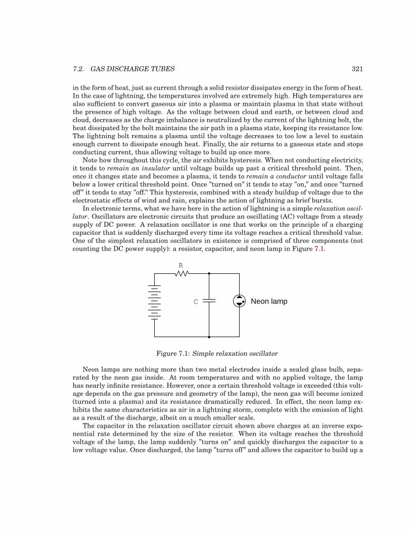
7.2. GAS DISCHARGE TUBES 321
in the form of heat, just as current through a solid resistor dissipates energy in the form of heat.In the case of lightning, the temperatures involved are extremely high. High temperatures arealso sufficient to convert gaseous air into a plasma or maintain plasma in that state withoutthe presence of high voltage. As the voltage between cloud and earth, or between cloud andcloud, decreases as the charge imbalance is neutralized by the current of the lightning bolt, theheat dissipated by the bolt maintains the air path in a plasma state, keeping its resistance low.The lightning bolt remains a plasma until the voltage decreases to too low a level to sustainenough current to dissipate enough heat. Finally, the air returns to a gaseous state and stopsconducting current, thus allowing voltage to build up once more.
Note how throughout this cycle, the air exhibits hysteresis. When not conducting electricity,it tends to remain an insulator until voltage builds up past a critical threshold point. Then,once it changes state and becomes a plasma, it tends to remain a conductor until voltage fallsbelow a lower critical threshold point. Once ”turned on” it tends to stay ”on,” and once ”turnedoff” it tends to stay ”off.” This hysteresis, combined with a steady buildup of voltage due to theelectrostatic effects of wind and rain, explains the action of lightning as brief bursts.
In electronic terms, what we have here in the action of lightning is a simple relaxation oscil-
lator. Oscillators are electronic circuits that produce an oscillating (AC) voltage from a steadysupply of DC power. A relaxation oscillator is one that works on the principle of a chargingcapacitor that is suddenly discharged every time its voltage reaches a critical threshold value.One of the simplest relaxation oscillators in existence is comprised of three components (notcounting the DC power supply): a resistor, capacitor, and neon lamp in Figure 7.1.
R
C Neon lamp
Figure 7.1: Simple relaxation oscillator
Neon lamps are nothing more than two metal electrodes inside a sealed glass bulb, sepa-rated by the neon gas inside. At room temperatures and with no applied voltage, the lamphas nearly infinite resistance. However, once a certain threshold voltage is exceeded (this volt-age depends on the gas pressure and geometry of the lamp), the neon gas will become ionized(turned into a plasma) and its resistance dramatically reduced. In effect, the neon lamp ex-hibits the same characteristics as air in a lightning storm, complete with the emission of lightas a result of the discharge, albeit on a much smaller scale.
The capacitor in the relaxation oscillator circuit shown above charges at an inverse expo-nential rate determined by the size of the resistor. When its voltage reaches the thresholdvoltage of the lamp, the lamp suddenly ”turns on” and quickly discharges the capacitor to alow voltage value. Once discharged, the lamp ”turns off” and allows the capacitor to build up a
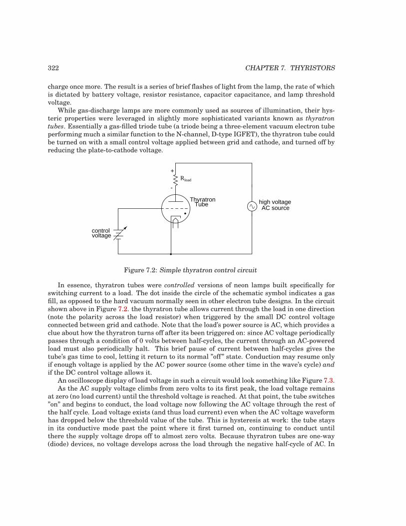
322 CHAPTER 7. THYRISTORS
charge once more. The result is a series of brief flashes of light from the lamp, the rate of whichis dictated by battery voltage, resistor resistance, capacitor capacitance, and lamp thresholdvoltage.
While gas-discharge lamps are more commonly used as sources of illumination, their hys-teric properties were leveraged in slightly more sophisticated variants known as thyratron
tubes. Essentially a gas-filled triode tube (a triode being a three-element vacuum electron tubeperforming much a similar function to the N-channel, D-type IGFET), the thyratron tube couldbe turned on with a small control voltage applied between grid and cathode, and turned off byreducing the plate-to-cathode voltage.
Rload
controlvoltage
ThyratronTube high voltage
AC source
+
-
Figure 7.2: Simple thyratron control circuit
In essence, thyratron tubes were controlled versions of neon lamps built specifically forswitching current to a load. The dot inside the circle of the schematic symbol indicates a gasfill, as opposed to the hard vacuum normally seen in other electron tube designs. In the circuitshown above in Figure 7.2. the thyratron tube allows current through the load in one direction(note the polarity across the load resistor) when triggered by the small DC control voltageconnected between grid and cathode. Note that the load’s power source is AC, which provides aclue about how the thyratron turns off after its been triggered on: since AC voltage periodicallypasses through a condition of 0 volts between half-cycles, the current through an AC-poweredload must also periodically halt. This brief pause of current between half-cycles gives thetube’s gas time to cool, letting it return to its normal ”off” state. Conduction may resume onlyif enough voltage is applied by the AC power source (some other time in the wave’s cycle) andif the DC control voltage allows it.
An oscilloscope display of load voltage in such a circuit would look something like Figure 7.3.As the AC supply voltage climbs from zero volts to its first peak, the load voltage remains
at zero (no load current) until the threshold voltage is reached. At that point, the tube switches”on” and begins to conduct, the load voltage now following the AC voltage through the rest ofthe half cycle. Load voltage exists (and thus load current) even when the AC voltage waveformhas dropped below the threshold value of the tube. This is hysteresis at work: the tube staysin its conductive mode past the point where it first turned on, continuing to conduct untilthere the supply voltage drops off to almost zero volts. Because thyratron tubes are one-way(diode) devices, no voltage develops across the load through the negative half-cycle of AC. In
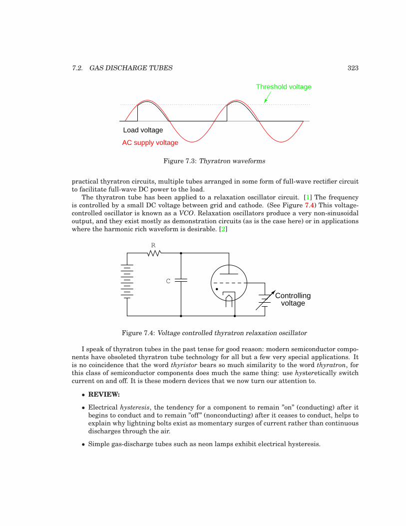
7.2. GAS DISCHARGE TUBES 323
AC supply voltage
Load voltage
Threshold voltage
Figure 7.3: Thyratron waveforms
practical thyratron circuits, multiple tubes arranged in some form of full-wave rectifier circuitto facilitate full-wave DC power to the load.
The thyratron tube has been applied to a relaxation oscillator circuit. [1] The frequencyis controlled by a small DC voltage between grid and cathode. (See Figure 7.4) This voltage-controlled oscillator is known as a VCO. Relaxation oscillators produce a very non-sinusoidaloutput, and they exist mostly as demonstration circuits (as is the case here) or in applicationswhere the harmonic rich waveform is desirable. [2]
R
C
Controllingvoltage
Figure 7.4: Voltage controlled thyratron relaxation oscillator
I speak of thyratron tubes in the past tense for good reason: modern semiconductor compo-nents have obsoleted thyratron tube technology for all but a few very special applications. Itis no coincidence that the word thyristor bears so much similarity to the word thyratron, forthis class of semiconductor components does much the same thing: use hysteretically switchcurrent on and off. It is these modern devices that we now turn our attention to.
• REVIEW:
• Electrical hysteresis, the tendency for a component to remain ”on” (conducting) after itbegins to conduct and to remain ”off” (nonconducting) after it ceases to conduct, helps toexplain why lightning bolts exist as momentary surges of current rather than continuousdischarges through the air.
• Simple gas-discharge tubes such as neon lamps exhibit electrical hysteresis.
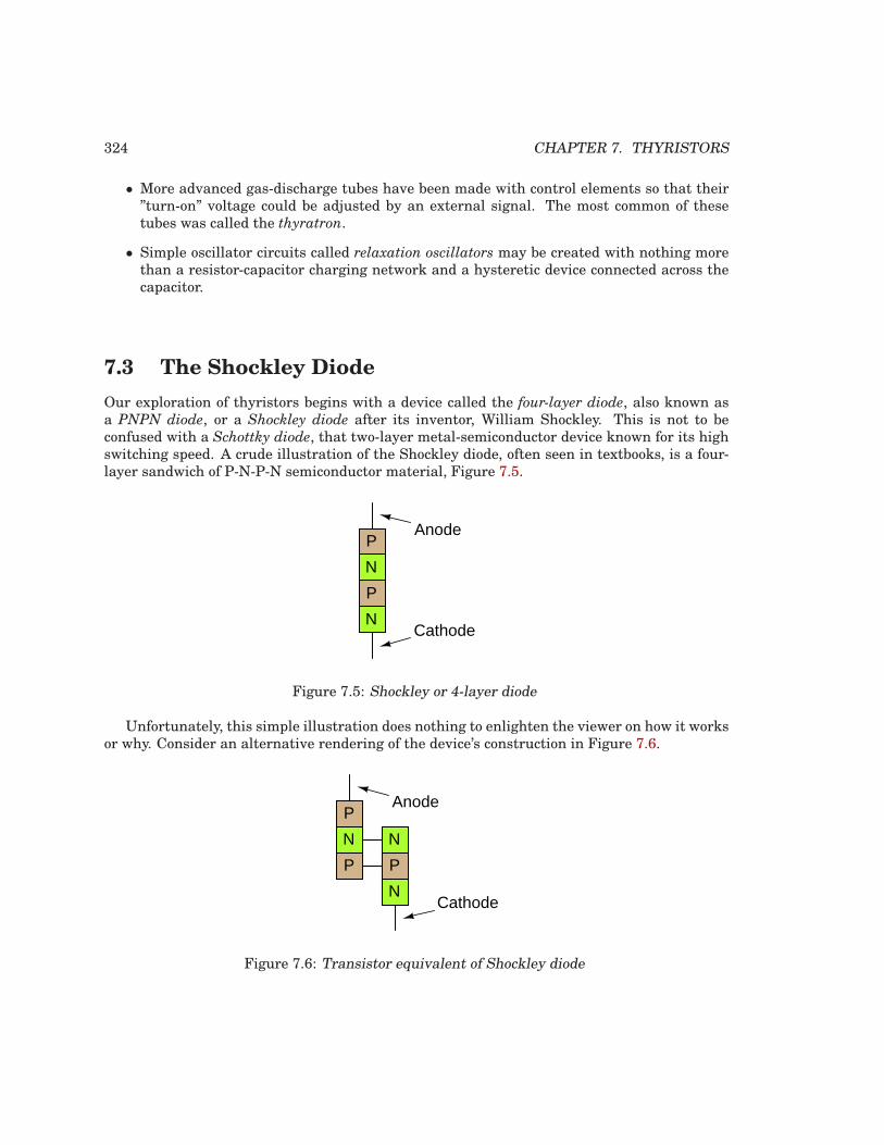
324 CHAPTER 7. THYRISTORS
• More advanced gas-discharge tubes have been made with control elements so that their”turn-on” voltage could be adjusted by an external signal. The most common of thesetubes was called the thyratron.
• Simple oscillator circuits called relaxation oscillators may be created with nothing morethan a resistor-capacitor charging network and a hysteretic device connected across thecapacitor.
7.3 The Shockley Diode
Our exploration of thyristors begins with a device called the four-layer diode, also known asa PNPN diode, or a Shockley diode after its inventor, William Shockley. This is not to beconfused with a Schottky diode, that two-layer metal-semiconductor device known for its highswitching speed. A crude illustration of the Shockley diode, often seen in textbooks, is a four-layer sandwich of P-N-P-N semiconductor material, Figure 7.5.
Anode
Cathode
P
P
N
N
Figure 7.5: Shockley or 4-layer diode
Unfortunately, this simple illustration does nothing to enlighten the viewer on how it worksor why. Consider an alternative rendering of the device’s construction in Figure 7.6.
Anode
Cathode
P
P
N
N
N
P
Figure 7.6: Transistor equivalent of Shockley diode
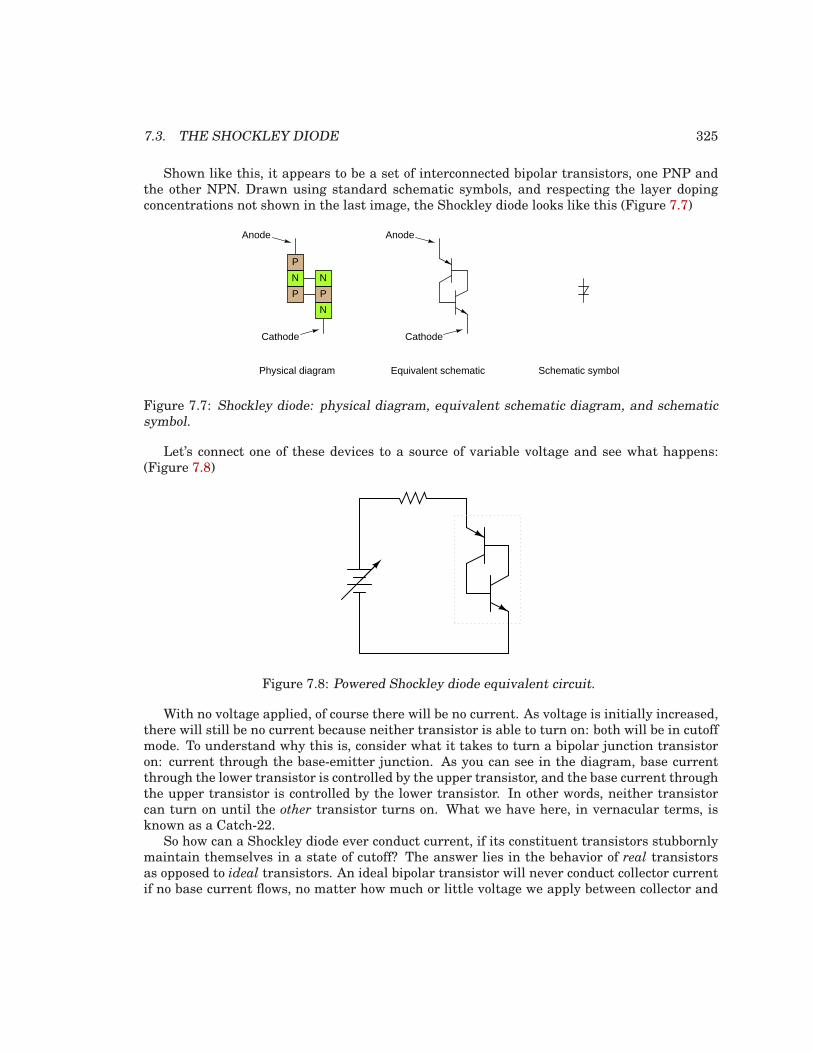
7.3. THE SHOCKLEY DIODE 325
Shown like this, it appears to be a set of interconnected bipolar transistors, one PNP andthe other NPN. Drawn using standard schematic symbols, and respecting the layer dopingconcentrations not shown in the last image, the Shockley diode looks like this (Figure 7.7)
Anode
Cathode Cathode
Anode
Physical diagram Equivalent schematic Schematic symbol
P
P
N
N
N
P
Figure 7.7: Shockley diode: physical diagram, equivalent schematic diagram, and schematicsymbol.
Let’s connect one of these devices to a source of variable voltage and see what happens:(Figure 7.8)
Figure 7.8: Powered Shockley diode equivalent circuit.
With no voltage applied, of course there will be no current. As voltage is initially increased,there will still be no current because neither transistor is able to turn on: both will be in cutoffmode. To understand why this is, consider what it takes to turn a bipolar junction transistoron: current through the base-emitter junction. As you can see in the diagram, base currentthrough the lower transistor is controlled by the upper transistor, and the base current throughthe upper transistor is controlled by the lower transistor. In other words, neither transistorcan turn on until the other transistor turns on. What we have here, in vernacular terms, isknown as a Catch-22.
So how can a Shockley diode ever conduct current, if its constituent transistors stubbornlymaintain themselves in a state of cutoff? The answer lies in the behavior of real transistorsas opposed to ideal transistors. An ideal bipolar transistor will never conduct collector currentif no base current flows, no matter how much or little voltage we apply between collector and
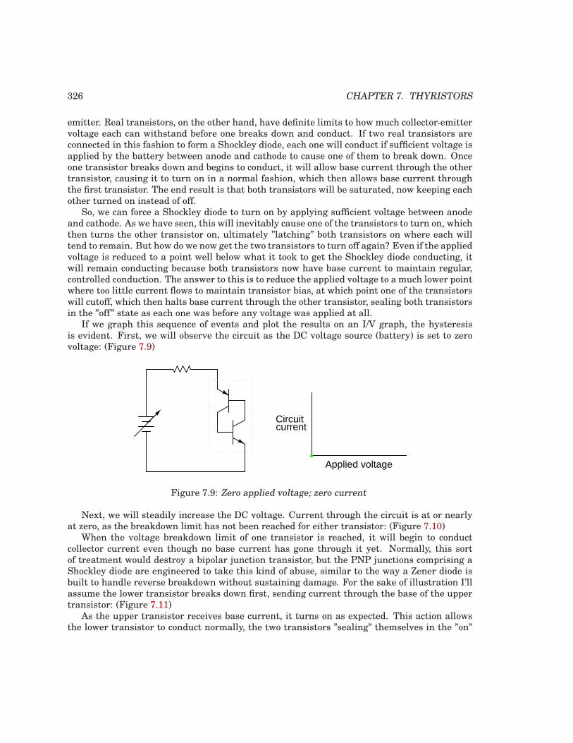
326 CHAPTER 7. THYRISTORS
emitter. Real transistors, on the other hand, have definite limits to how much collector-emittervoltage each can withstand before one breaks down and conduct. If two real transistors areconnected in this fashion to form a Shockley diode, each one will conduct if sufficient voltage isapplied by the battery between anode and cathode to cause one of them to break down. Onceone transistor breaks down and begins to conduct, it will allow base current through the othertransistor, causing it to turn on in a normal fashion, which then allows base current throughthe first transistor. The end result is that both transistors will be saturated, now keeping eachother turned on instead of off.
So, we can force a Shockley diode to turn on by applying sufficient voltage between anodeand cathode. As we have seen, this will inevitably cause one of the transistors to turn on, whichthen turns the other transistor on, ultimately ”latching” both transistors on where each willtend to remain. But how do we now get the two transistors to turn off again? Even if the appliedvoltage is reduced to a point well below what it took to get the Shockley diode conducting, itwill remain conducting because both transistors now have base current to maintain regular,controlled conduction. The answer to this is to reduce the applied voltage to a much lower pointwhere too little current flows to maintain transistor bias, at which point one of the transistorswill cutoff, which then halts base current through the other transistor, sealing both transistorsin the ”off” state as each one was before any voltage was applied at all.
If we graph this sequence of events and plot the results on an I/V graph, the hysteresisis evident. First, we will observe the circuit as the DC voltage source (battery) is set to zerovoltage: (Figure 7.9)
Applied voltage
Circuitcurrent
Figure 7.9: Zero applied voltage; zero current
Next, we will steadily increase the DC voltage. Current through the circuit is at or nearlyat zero, as the breakdown limit has not been reached for either transistor: (Figure 7.10)
When the voltage breakdown limit of one transistor is reached, it will begin to conductcollector current even though no base current has gone through it yet. Normally, this sortof treatment would destroy a bipolar junction transistor, but the PNP junctions comprising aShockley diode are engineered to take this kind of abuse, similar to the way a Zener diode isbuilt to handle reverse breakdown without sustaining damage. For the sake of illustration I’llassume the lower transistor breaks down first, sending current through the base of the uppertransistor: (Figure 7.11)
As the upper transistor receives base current, it turns on as expected. This action allowsthe lower transistor to conduct normally, the two transistors ”sealing” themselves in the ”on”
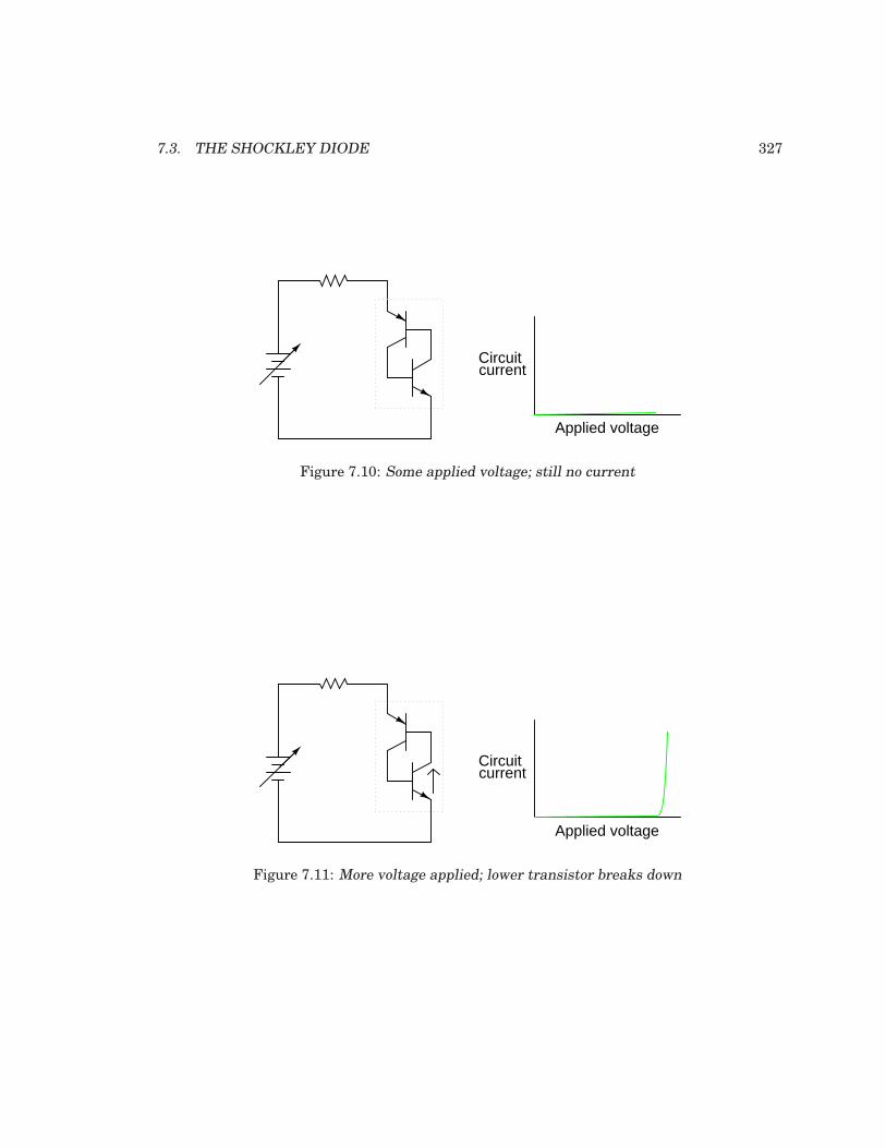
7.3. THE SHOCKLEY DIODE 327
Applied voltage
Circuitcurrent
Figure 7.10: Some applied voltage; still no current
Applied voltage
Circuitcurrent
Figure 7.11: More voltage applied; lower transistor breaks down
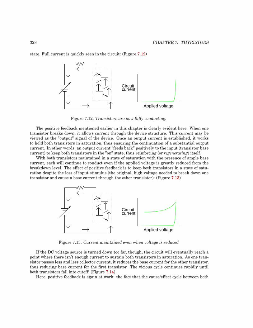
328 CHAPTER 7. THYRISTORS
state. Full current is quickly seen in the circuit: (Figure 7.12)
Applied voltage
Circuitcurrent
Figure 7.12: Transistors are now fully conducting.
The positive feedback mentioned earlier in this chapter is clearly evident here. When onetransistor breaks down, it allows current through the device structure. This current may beviewed as the ”output” signal of the device. Once an output current is established, it worksto hold both transistors in saturation, thus ensuring the continuation of a substantial outputcurrent. In other words, an output current ”feeds back” positively to the input (transistor basecurrent) to keep both transistors in the ”on” state, thus reinforcing (or regenerating) itself.
With both transistors maintained in a state of saturation with the presence of ample basecurrent, each will continue to conduct even if the applied voltage is greatly reduced from thebreakdown level. The effect of positive feedback is to keep both transistors in a state of satu-ration despite the loss of input stimulus (the original, high voltage needed to break down onetransistor and cause a base current through the other transistor): (Figure 7.13)
Applied voltage
Circuitcurrent
Figure 7.13: Current maintained even when voltage is reduced
If the DC voltage source is turned down too far, though, the circuit will eventually reach apoint where there isn’t enough current to sustain both transistors in saturation. As one tran-sistor passes less and less collector current, it reduces the base current for the other transistor,thus reducing base current for the first transistor. The vicious cycle continues rapidly untilboth transistors fall into cutoff: (Figure 7.14)
Here, positive feedback is again at work: the fact that the cause/effect cycle between both
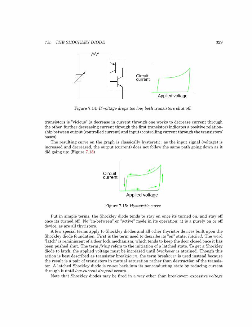
7.3. THE SHOCKLEY DIODE 329
Applied voltage
Circuitcurrent
Figure 7.14: If voltage drops too low, both transistors shut off.
transistors is ”vicious” (a decrease in current through one works to decrease current throughthe other, further decreasing current through the first transistor) indicates a positive relation-ship between output (controlled current) and input (controlling current through the transistors’bases).
The resulting curve on the graph is classically hysteretic: as the input signal (voltage) isincreased and decreased, the output (current) does not follow the same path going down as itdid going up: (Figure 7.15)
Applied voltage
Circuitcurrent
Figure 7.15: Hysteretic curve
Put in simple terms, the Shockley diode tends to stay on once its turned on, and stay offonce its turned off. No ”in-between” or ”active” mode in its operation: it is a purely on or offdevice, as are all thyristors.
A few special terms apply to Shockley diodes and all other thyristor devices built upon theShockley diode foundation. First is the term used to describe its ”on” state: latched. The word”latch” is reminiscent of a door lock mechanism, which tends to keep the door closed once it hasbeen pushed shut. The term firing refers to the initiation of a latched state. To get a Shockleydiode to latch, the applied voltage must be increased until breakover is attained. Though thisaction is best described as transistor breakdown, the term breakover is used instead becausethe result is a pair of transistors in mutual saturation rather than destruction of the transis-tor. A latched Shockley diode is re-set back into its nonconducting state by reducing currentthrough it until low-current dropout occurs.
Note that Shockley diodes may be fired in a way other than breakover: excessive voltage
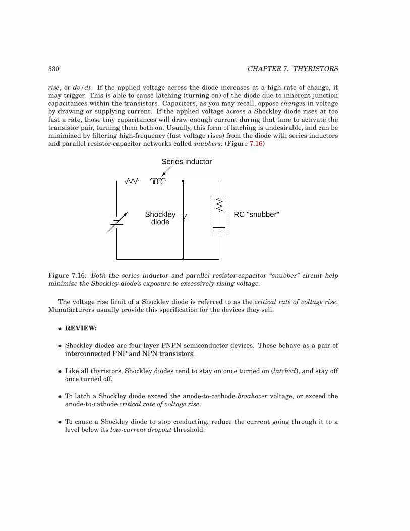
330 CHAPTER 7. THYRISTORS
rise, or dv/dt. If the applied voltage across the diode increases at a high rate of change, itmay trigger. This is able to cause latching (turning on) of the diode due to inherent junctioncapacitances within the transistors. Capacitors, as you may recall, oppose changes in voltageby drawing or supplying current. If the applied voltage across a Shockley diode rises at toofast a rate, those tiny capacitances will draw enough current during that time to activate thetransistor pair, turning them both on. Usually, this form of latching is undesirable, and can beminimized by filtering high-frequency (fast voltage rises) from the diode with series inductorsand parallel resistor-capacitor networks called snubbers: (Figure 7.16)
RC "snubber"
Series inductor
Shockleydiode
Figure 7.16: Both the series inductor and parallel resistor-capacitor “snubber” circuit helpminimize the Shockley diode’s exposure to excessively rising voltage.
The voltage rise limit of a Shockley diode is referred to as the critical rate of voltage rise.Manufacturers usually provide this specification for the devices they sell.
• REVIEW:
• Shockley diodes are four-layer PNPN semiconductor devices. These behave as a pair ofinterconnected PNP and NPN transistors.
• Like all thyristors, Shockley diodes tend to stay on once turned on (latched), and stay offonce turned off.
• To latch a Shockley diode exceed the anode-to-cathode breakover voltage, or exceed theanode-to-cathode critical rate of voltage rise.
• To cause a Shockley diode to stop conducting, reduce the current going through it to alevel below its low-current dropout threshold.
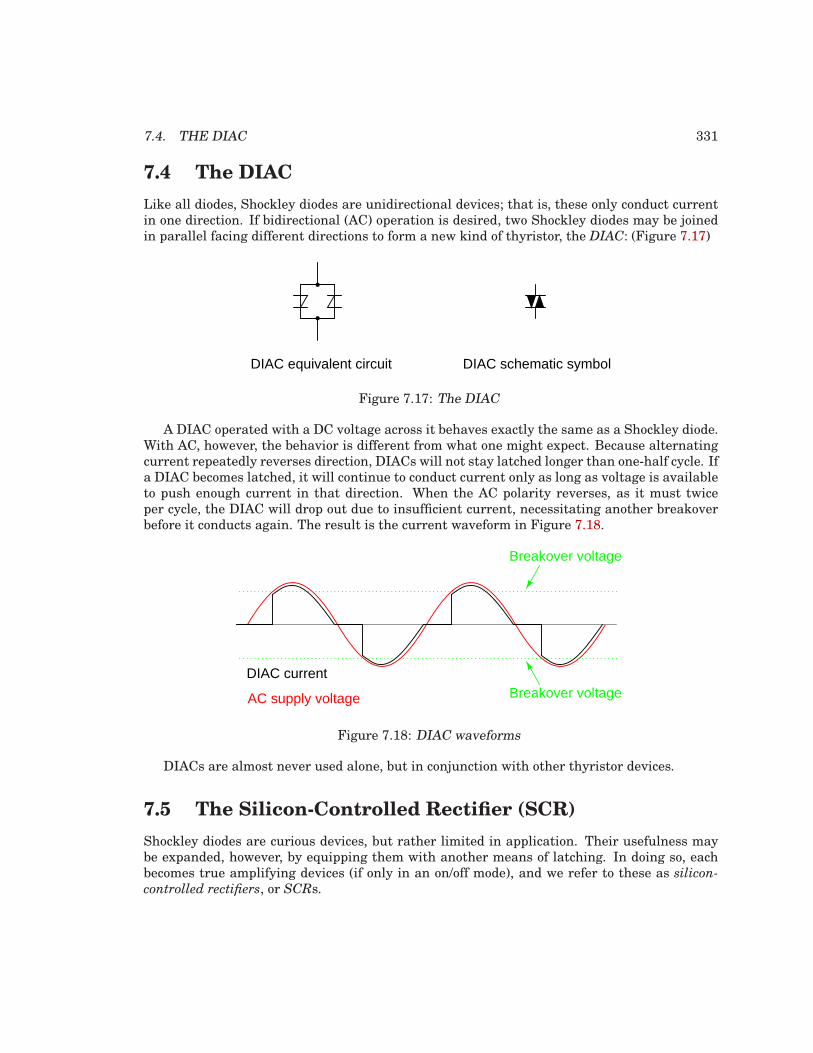
7.4. THE DIAC 331
7.4 The DIAC
Like all diodes, Shockley diodes are unidirectional devices; that is, these only conduct currentin one direction. If bidirectional (AC) operation is desired, two Shockley diodes may be joinedin parallel facing different directions to form a new kind of thyristor, the DIAC: (Figure 7.17)
DIAC equivalent circuit DIAC schematic symbol
Figure 7.17: The DIAC
A DIAC operated with a DC voltage across it behaves exactly the same as a Shockley diode.With AC, however, the behavior is different from what one might expect. Because alternatingcurrent repeatedly reverses direction, DIACs will not stay latched longer than one-half cycle. Ifa DIAC becomes latched, it will continue to conduct current only as long as voltage is availableto push enough current in that direction. When the AC polarity reverses, as it must twiceper cycle, the DIAC will drop out due to insufficient current, necessitating another breakoverbefore it conducts again. The result is the current waveform in Figure 7.18.
AC supply voltage
DIAC current
Breakover voltage
Breakover voltage
Figure 7.18: DIAC waveforms
DIACs are almost never used alone, but in conjunction with other thyristor devices.
7.5 The Silicon-Controlled Rectifier (SCR)
Shockley diodes are curious devices, but rather limited in application. Their usefulness maybe expanded, however, by equipping them with another means of latching. In doing so, eachbecomes true amplifying devices (if only in an on/off mode), and we refer to these as silicon-
controlled rectifiers, or SCRs.
332 CHAPTER 7. THYRISTORS
The progression from Shockley diode to SCR is achieved with one small addition, actuallynothing more than a third wire connection to the existing PNPN structure: (Figure 7.19)
Anode
Cathode Cathode
Anode
Physical diagram Equivalent schematic Schematic symbol
GateGate
Cathode
Gate
AnodeP
P
N
N
N
P
Figure 7.19: The Silicon-Controlled Rectifier (SCR)
If an SCR’s gate is left floating (disconnected), it behaves exactly as a Shockley diode. Itmay be latched by breakover voltage or by exceeding the critical rate of voltage rise betweenanode and cathode, just as with the Shockley diode. Dropout is accomplished by reducingcurrent until one or both internal transistors fall into cutoff mode, also like the Shockley diode.However, because the gate terminal connects directly to the base of the lower transistor, itmay be used as an alternative means to latch the SCR. By applying a small voltage betweengate and cathode, the lower transistor will be forced on by the resulting base current, whichwill cause the upper transistor to conduct, which then supplies the lower transistor’s basewith current so that it no longer needs to be activated by a gate voltage. The necessary gatecurrent to initiate latch-up, of course, will be much lower than the current through the SCRfrom cathode to anode, so the SCR does achieve a measure of amplification.
This method of securing SCR conduction is called triggering, and it is by far the most com-mon way that SCRs are latched in actual practice. In fact, SCRs are usually chosen so thattheir breakover voltage is far beyond the greatest voltage expected to be experienced from thepower source, so that it can be turned on only by an intentional voltage pulse applied to thegate.
It should be mentioned that SCRs may sometimes be turned off by directly shorting theirgate and cathode terminals together, or by ”reverse-triggering” the gate with a negative voltage(in reference to the cathode), so that the lower transistor is forced into cutoff. I say this is”sometimes” possible because it involves shunting all of the upper transistor’s collector currentpast the lower transistor’s base. This current may be substantial, making triggered shut-offof an SCR difficult at best. A variation of the SCR, called a Gate-Turn-Off thyristor, or GTO,makes this task easier. But even with a GTO, the gate current required to turn it off may beas much as 20% of the anode (load) current! The schematic symbol for a GTO is shown in thefollowing illustration: (Figure 7.20)
SCRs and GTOs share the same equivalent schematics (two transistors connected in apositive-feedback fashion), the only differences being details of construction designed to grantthe NPN transistor a greater β than the PNP. This allows a smaller gate current (forward orreverse) to exert a greater degree of control over conduction from cathode to anode, with thePNP transistor’s latched state being more dependent upon the NPN’s than vice versa. The
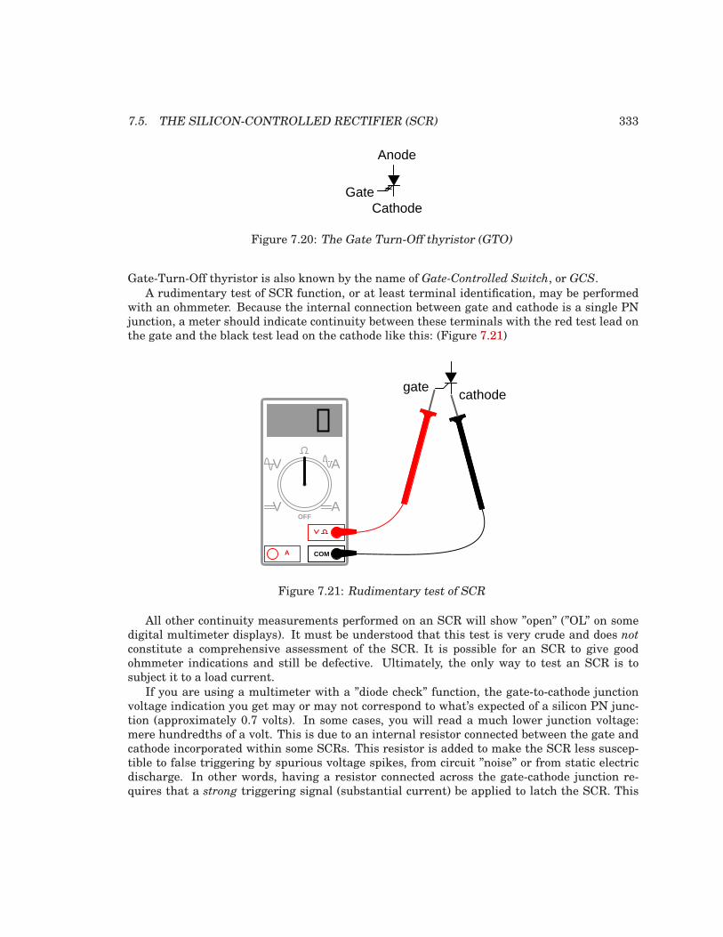
7.5. THE SILICON-CONTROLLED RECTIFIER (SCR) 333
Anode
GateCathode
Figure 7.20: The Gate Turn-Off thyristor (GTO)
Gate-Turn-Off thyristor is also known by the name of Gate-Controlled Switch, or GCS.A rudimentary test of SCR function, or at least terminal identification, may be performed
with an ohmmeter. Because the internal connection between gate and cathode is a single PNjunction, a meter should indicate continuity between these terminals with the red test lead onthe gate and the black test lead on the cathode like this: (Figure 7.21)
COMA
V
V A
AOFF
gatecathode
Figure 7.21: Rudimentary test of SCR
All other continuity measurements performed on an SCR will show ”open” (”OL” on somedigital multimeter displays). It must be understood that this test is very crude and does not
constitute a comprehensive assessment of the SCR. It is possible for an SCR to give goodohmmeter indications and still be defective. Ultimately, the only way to test an SCR is tosubject it to a load current.
If you are using a multimeter with a ”diode check” function, the gate-to-cathode junctionvoltage indication you get may or may not correspond to what’s expected of a silicon PN junc-tion (approximately 0.7 volts). In some cases, you will read a much lower junction voltage:mere hundredths of a volt. This is due to an internal resistor connected between the gate andcathode incorporated within some SCRs. This resistor is added to make the SCR less suscep-tible to false triggering by spurious voltage spikes, from circuit ”noise” or from static electricdischarge. In other words, having a resistor connected across the gate-cathode junction re-quires that a strong triggering signal (substantial current) be applied to latch the SCR. This
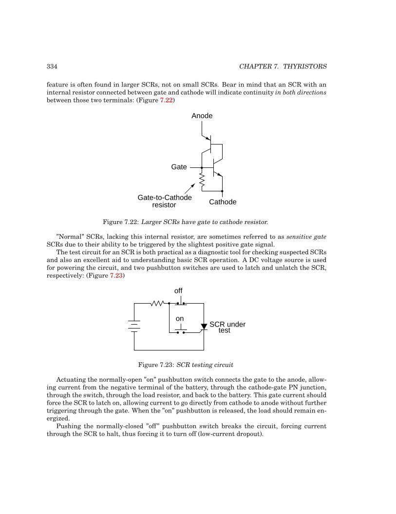
334 CHAPTER 7. THYRISTORS
feature is often found in larger SCRs, not on small SCRs. Bear in mind that an SCR with aninternal resistor connected between gate and cathode will indicate continuity in both directions
between those two terminals: (Figure 7.22)
Cathode
Anode
Gate
Gate-to-Cathoderesistor
Figure 7.22: Larger SCRs have gate to cathode resistor.
”Normal” SCRs, lacking this internal resistor, are sometimes referred to as sensitive gate
SCRs due to their ability to be triggered by the slightest positive gate signal.The test circuit for an SCR is both practical as a diagnostic tool for checking suspected SCRs
and also an excellent aid to understanding basic SCR operation. A DC voltage source is usedfor powering the circuit, and two pushbutton switches are used to latch and unlatch the SCR,respectively: (Figure 7.23)
SCR undertest
on
off
Figure 7.23: SCR testing circuit
Actuating the normally-open ”on” pushbutton switch connects the gate to the anode, allow-ing current from the negative terminal of the battery, through the cathode-gate PN junction,through the switch, through the load resistor, and back to the battery. This gate current shouldforce the SCR to latch on, allowing current to go directly from cathode to anode without furthertriggering through the gate. When the ”on” pushbutton is released, the load should remain en-ergized.
Pushing the normally-closed ”off” pushbutton switch breaks the circuit, forcing currentthrough the SCR to halt, thus forcing it to turn off (low-current dropout).
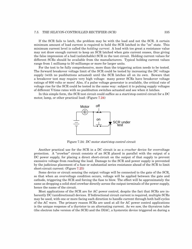
7.5. THE SILICON-CONTROLLED RECTIFIER (SCR) 335
If the SCR fails to latch, the problem may be with the load and not the SCR. A certainminimum amount of load current is required to hold the SCR latched in the ”on” state. Thisminimum current level is called the holding current. A load with too great a resistance valuemay not draw enough current to keep an SCR latched when gate current ceases, thus givingthe false impression of a bad (unlatchable) SCR in the test circuit. Holding current values fordifferent SCRs should be available from the manufacturers. Typical holding current valuesrange from 1 milliamp to 50 milliamps or more for larger units.
For the test to be fully comprehensive, more than the triggering action needs to be tested.The forward breakover voltage limit of the SCR could be tested by increasing the DC voltagesupply (with no pushbuttons actuated) until the SCR latches all on its own. Beware thata breakover test may require very high voltage: many power SCRs have breakover voltageratings of 600 volts or more! Also, if a pulse voltage generator is available, the critical rate ofvoltage rise for the SCR could be tested in the same way: subject it to pulsing supply voltagesof different V/time rates with no pushbutton switches actuated and see when it latches.
In this simple form, the SCR test circuit could suffice as a start/stop control circuit for a DCmotor, lamp, or other practical load: (Figure 7.24)
SCR undertest
on
offMotor
Figure 7.24: DC motor start/stop control circuit
Another practical use for the SCR in a DC circuit is as a crowbar device for overvoltageprotection. A ”crowbar” circuit consists of an SCR placed in parallel with the output of aDC power supply, for placing a direct short-circuit on the output of that supply to preventexcessive voltage from reaching the load. Damage to the SCR and power supply is preventedby the judicious placement of a fuse or substantial series resistance ahead of the SCR to limitshort-circuit current: (Figure 7.25)
Some device or circuit sensing the output voltage will be connected to the gate of the SCR,so that when an overvoltage condition occurs, voltage will be applied between the gate andcathode, triggering the SCR and forcing the fuse to blow. The effect will be approximately thesame as dropping a solid steel crowbar directly across the output terminals of the power supply,hence the name of the circuit.
Most applications of the SCR are for AC power control, despite the fact that SCRs are in-herently DC (unidirectional) devices. If bidirectional circuit current is required, multiple SCRsmay be used, with one or more facing each direction to handle current through both half-cyclesof the AC wave. The primary reason SCRs are used at all for AC power control applicationsis the unique response of a thyristor to an alternating current. As we saw, the thyratron tube(the electron tube version of the SCR) and the DIAC, a hysteretic device triggered on during a
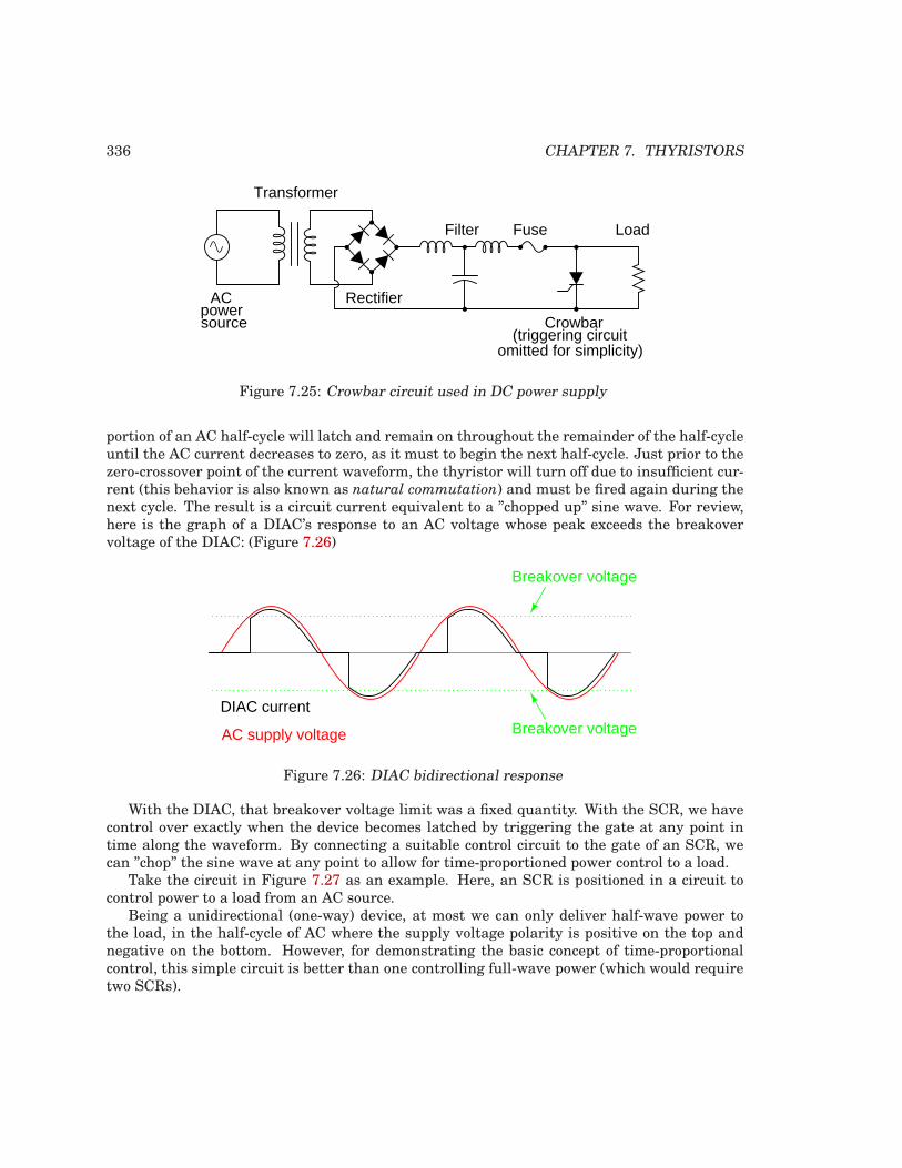
336 CHAPTER 7. THYRISTORS
Transformer
Rectifier
Filter
ACpowersource
Fuse
Crowbar
Load
(triggering circuitomitted for simplicity)
Figure 7.25: Crowbar circuit used in DC power supply
portion of an AC half-cycle will latch and remain on throughout the remainder of the half-cycleuntil the AC current decreases to zero, as it must to begin the next half-cycle. Just prior to thezero-crossover point of the current waveform, the thyristor will turn off due to insufficient cur-rent (this behavior is also known as natural commutation) and must be fired again during thenext cycle. The result is a circuit current equivalent to a ”chopped up” sine wave. For review,here is the graph of a DIAC’s response to an AC voltage whose peak exceeds the breakovervoltage of the DIAC: (Figure 7.26)
AC supply voltage
DIAC current
Breakover voltage
Breakover voltage
Figure 7.26: DIAC bidirectional response
With the DIAC, that breakover voltage limit was a fixed quantity. With the SCR, we havecontrol over exactly when the device becomes latched by triggering the gate at any point intime along the waveform. By connecting a suitable control circuit to the gate of an SCR, wecan ”chop” the sine wave at any point to allow for time-proportioned power control to a load.
Take the circuit in Figure 7.27 as an example. Here, an SCR is positioned in a circuit tocontrol power to a load from an AC source.
Being a unidirectional (one-way) device, at most we can only deliver half-wave power tothe load, in the half-cycle of AC where the supply voltage polarity is positive on the top andnegative on the bottom. However, for demonstrating the basic concept of time-proportionalcontrol, this simple circuit is better than one controlling full-wave power (which would requiretwo SCRs).
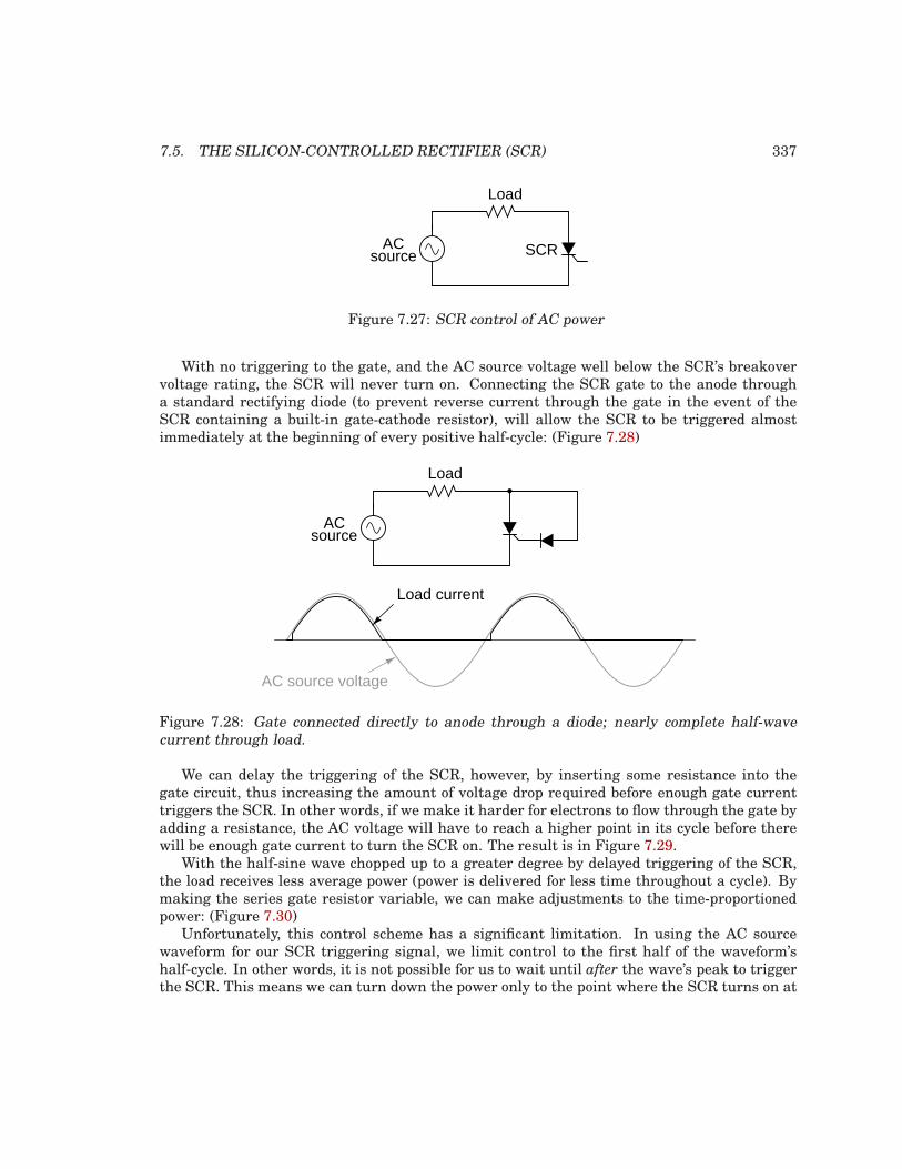
7.5. THE SILICON-CONTROLLED RECTIFIER (SCR) 337
Load
ACsource SCR
Figure 7.27: SCR control of AC power
With no triggering to the gate, and the AC source voltage well below the SCR’s breakovervoltage rating, the SCR will never turn on. Connecting the SCR gate to the anode througha standard rectifying diode (to prevent reverse current through the gate in the event of theSCR containing a built-in gate-cathode resistor), will allow the SCR to be triggered almostimmediately at the beginning of every positive half-cycle: (Figure 7.28)
Load
ACsource
AC source voltage
Load current
Figure 7.28: Gate connected directly to anode through a diode; nearly complete half-wavecurrent through load.
We can delay the triggering of the SCR, however, by inserting some resistance into thegate circuit, thus increasing the amount of voltage drop required before enough gate currenttriggers the SCR. In other words, if we make it harder for electrons to flow through the gate byadding a resistance, the AC voltage will have to reach a higher point in its cycle before therewill be enough gate current to turn the SCR on. The result is in Figure 7.29.
With the half-sine wave chopped up to a greater degree by delayed triggering of the SCR,the load receives less average power (power is delivered for less time throughout a cycle). Bymaking the series gate resistor variable, we can make adjustments to the time-proportionedpower: (Figure 7.30)
Unfortunately, this control scheme has a significant limitation. In using the AC sourcewaveform for our SCR triggering signal, we limit control to the first half of the waveform’shalf-cycle. In other words, it is not possible for us to wait until after the wave’s peak to triggerthe SCR. This means we can turn down the power only to the point where the SCR turns on at
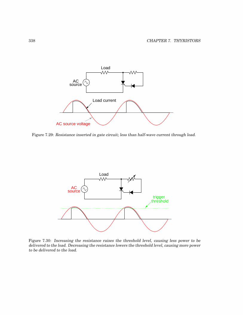
338 CHAPTER 7. THYRISTORS
Load
ACsource
AC source voltage
Load current
Figure 7.29: Resistance inserted in gate circuit; less than half-wave current through load.
Load
ACsource
triggerthreshold
Figure 7.30: Increasing the resistance raises the threshold level, causing less power to bedelivered to the load. Decreasing the resistance lowers the threshold level, causing more powerto be delivered to the load.
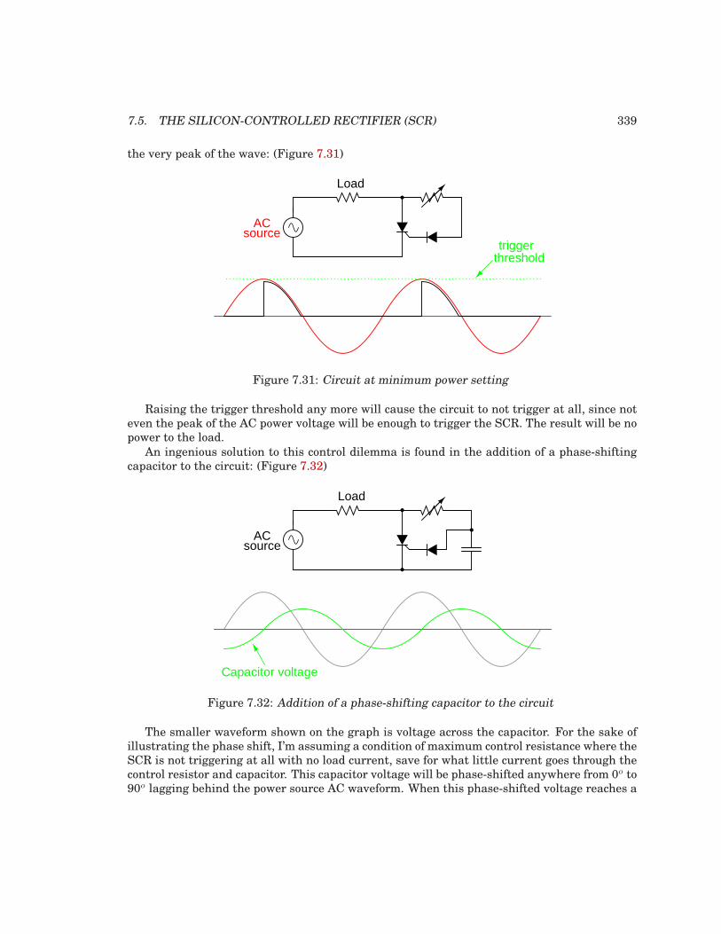
7.5. THE SILICON-CONTROLLED RECTIFIER (SCR) 339
the very peak of the wave: (Figure 7.31)
Load
ACsource
triggerthreshold
Figure 7.31: Circuit at minimum power setting
Raising the trigger threshold any more will cause the circuit to not trigger at all, since noteven the peak of the AC power voltage will be enough to trigger the SCR. The result will be nopower to the load.
An ingenious solution to this control dilemma is found in the addition of a phase-shiftingcapacitor to the circuit: (Figure 7.32)
Load
ACsource
Capacitor voltage
Figure 7.32: Addition of a phase-shifting capacitor to the circuit
The smaller waveform shown on the graph is voltage across the capacitor. For the sake ofillustrating the phase shift, I’m assuming a condition of maximum control resistance where theSCR is not triggering at all with no load current, save for what little current goes through thecontrol resistor and capacitor. This capacitor voltage will be phase-shifted anywhere from 0o to90o lagging behind the power source AC waveform. When this phase-shifted voltage reaches a
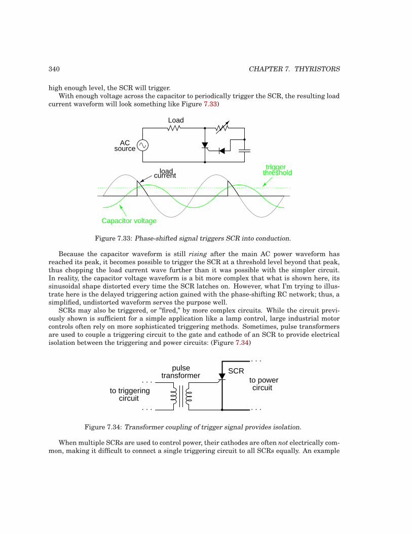
340 CHAPTER 7. THYRISTORS
high enough level, the SCR will trigger.With enough voltage across the capacitor to periodically trigger the SCR, the resulting load
current waveform will look something like Figure 7.33)
Load
ACsource
Capacitor voltage
triggerthresholdload
current
Figure 7.33: Phase-shifted signal triggers SCR into conduction.
Because the capacitor waveform is still rising after the main AC power waveform hasreached its peak, it becomes possible to trigger the SCR at a threshold level beyond that peak,thus chopping the load current wave further than it was possible with the simpler circuit.In reality, the capacitor voltage waveform is a bit more complex that what is shown here, itssinusoidal shape distorted every time the SCR latches on. However, what I’m trying to illus-trate here is the delayed triggering action gained with the phase-shifting RC network; thus, asimplified, undistorted waveform serves the purpose well.
SCRs may also be triggered, or ”fired,” by more complex circuits. While the circuit previ-ously shown is sufficient for a simple application like a lamp control, large industrial motorcontrols often rely on more sophisticated triggering methods. Sometimes, pulse transformersare used to couple a triggering circuit to the gate and cathode of an SCR to provide electricalisolation between the triggering and power circuits: (Figure 7.34)
. . .
. . .
to triggeringcircuit
. . .
. . .
to powercircuit
pulsetransformer
SCR
Figure 7.34: Transformer coupling of trigger signal provides isolation.
Whenmultiple SCRs are used to control power, their cathodes are often not electrically com-mon, making it difficult to connect a single triggering circuit to all SCRs equally. An example
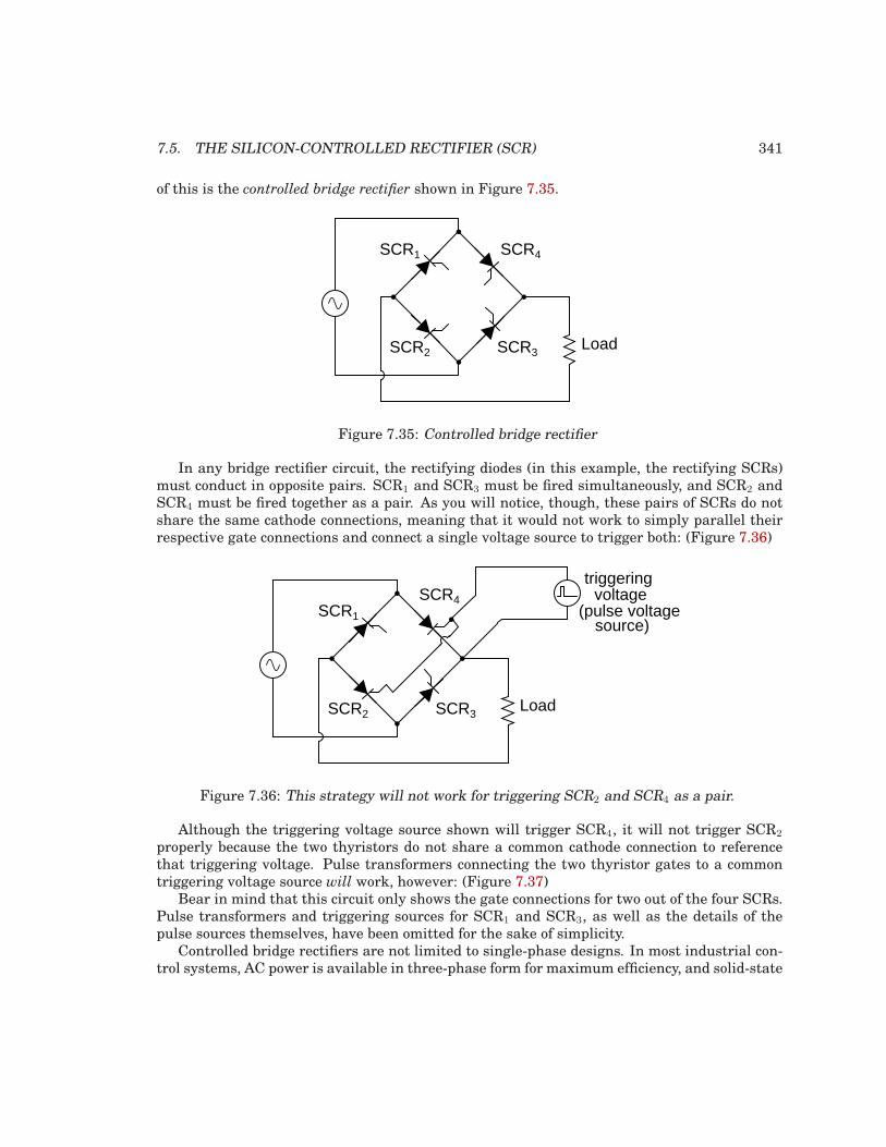
7.5. THE SILICON-CONTROLLED RECTIFIER (SCR) 341
of this is the controlled bridge rectifier shown in Figure 7.35.
Load
SCR1
SCR2 SCR3
SCR4
Figure 7.35: Controlled bridge rectifier
In any bridge rectifier circuit, the rectifying diodes (in this example, the rectifying SCRs)must conduct in opposite pairs. SCR1 and SCR3 must be fired simultaneously, and SCR2 andSCR4 must be fired together as a pair. As you will notice, though, these pairs of SCRs do notshare the same cathode connections, meaning that it would not work to simply parallel theirrespective gate connections and connect a single voltage source to trigger both: (Figure 7.36)
Load
SCR1
SCR2 SCR3
SCR4
triggeringvoltage
(pulse voltagesource)
Figure 7.36: This strategy will not work for triggering SCR2 and SCR4 as a pair.
Although the triggering voltage source shown will trigger SCR4, it will not trigger SCR2
properly because the two thyristors do not share a common cathode connection to referencethat triggering voltage. Pulse transformers connecting the two thyristor gates to a commontriggering voltage source will work, however: (Figure 7.37)
Bear in mind that this circuit only shows the gate connections for two out of the four SCRs.Pulse transformers and triggering sources for SCR1 and SCR3, as well as the details of thepulse sources themselves, have been omitted for the sake of simplicity.
Controlled bridge rectifiers are not limited to single-phase designs. In most industrial con-trol systems, AC power is available in three-phase form for maximum efficiency, and solid-state
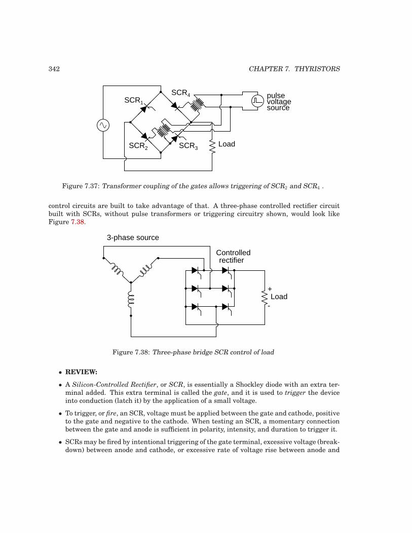
342 CHAPTER 7. THYRISTORS
Load
SCR1
SCR2 SCR3
SCR4 pulsevoltagesource
Figure 7.37: Transformer coupling of the gates allows triggering of SCR2 and SCR4 .
control circuits are built to take advantage of that. A three-phase controlled rectifier circuitbuilt with SCRs, without pulse transformers or triggering circuitry shown, would look likeFigure 7.38.
Load
3-phase source
Controlledrectifier
+
-
Figure 7.38: Three-phase bridge SCR control of load
• REVIEW:
• A Silicon-Controlled Rectifier, or SCR, is essentially a Shockley diode with an extra ter-minal added. This extra terminal is called the gate, and it is used to trigger the deviceinto conduction (latch it) by the application of a small voltage.
• To trigger, or fire, an SCR, voltage must be applied between the gate and cathode, positiveto the gate and negative to the cathode. When testing an SCR, a momentary connectionbetween the gate and anode is sufficient in polarity, intensity, and duration to trigger it.
• SCRsmay be fired by intentional triggering of the gate terminal, excessive voltage (break-down) between anode and cathode, or excessive rate of voltage rise between anode and
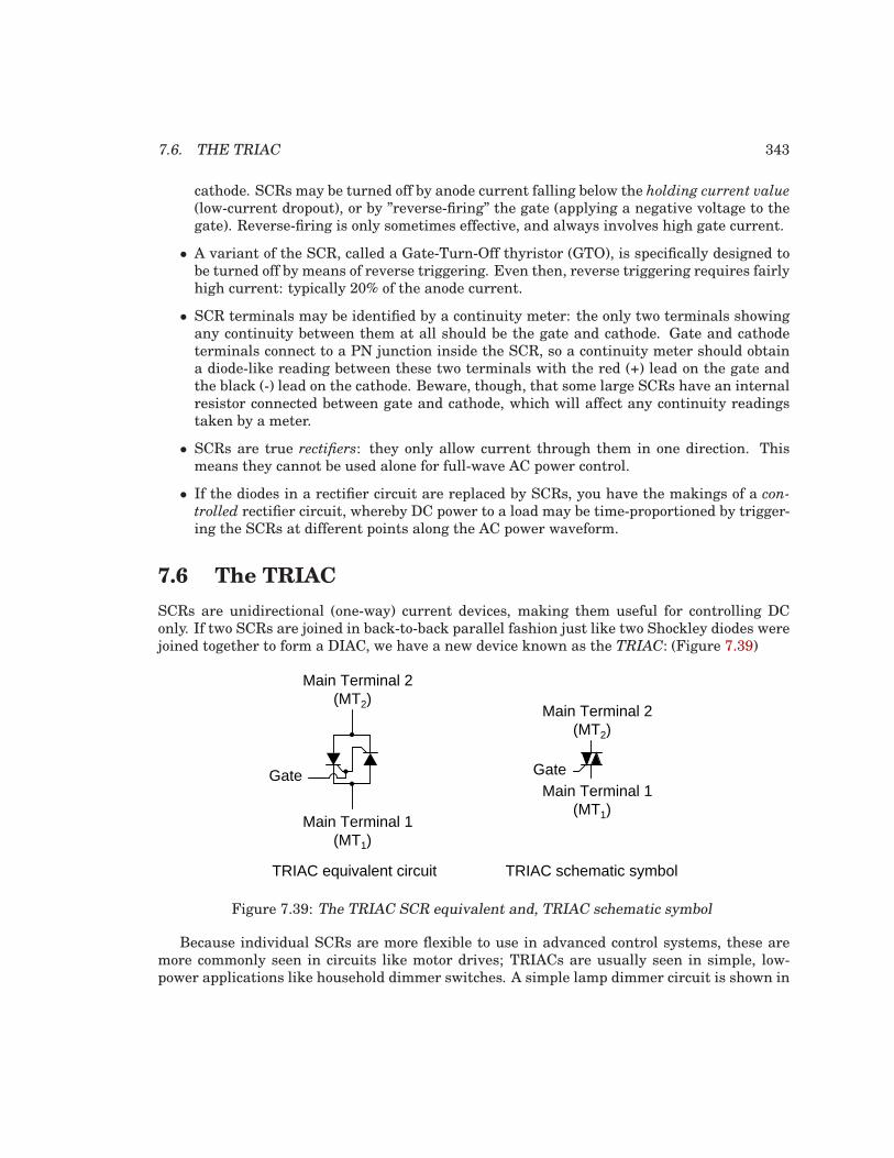
7.6. THE TRIAC 343
cathode. SCRs may be turned off by anode current falling below the holding current value
(low-current dropout), or by ”reverse-firing” the gate (applying a negative voltage to thegate). Reverse-firing is only sometimes effective, and always involves high gate current.
• A variant of the SCR, called a Gate-Turn-Off thyristor (GTO), is specifically designed tobe turned off by means of reverse triggering. Even then, reverse triggering requires fairlyhigh current: typically 20% of the anode current.
• SCR terminals may be identified by a continuity meter: the only two terminals showingany continuity between them at all should be the gate and cathode. Gate and cathodeterminals connect to a PN junction inside the SCR, so a continuity meter should obtaina diode-like reading between these two terminals with the red (+) lead on the gate andthe black (-) lead on the cathode. Beware, though, that some large SCRs have an internalresistor connected between gate and cathode, which will affect any continuity readingstaken by a meter.
• SCRs are true rectifiers: they only allow current through them in one direction. Thismeans they cannot be used alone for full-wave AC power control.
• If the diodes in a rectifier circuit are replaced by SCRs, you have the makings of a con-
trolled rectifier circuit, whereby DC power to a load may be time-proportioned by trigger-ing the SCRs at different points along the AC power waveform.
7.6 The TRIAC
SCRs are unidirectional (one-way) current devices, making them useful for controlling DConly. If two SCRs are joined in back-to-back parallel fashion just like two Shockley diodes werejoined together to form a DIAC, we have a new device known as the TRIAC: (Figure 7.39)
TRIAC equivalent circuit TRIAC schematic symbol
Gate
Main Terminal 1
Main Terminal 2(MT2)
(MT1)
Main Terminal 2(MT2)
Main Terminal 1(MT1)
Gate
Figure 7.39: The TRIAC SCR equivalent and, TRIAC schematic symbol
Because individual SCRs are more flexible to use in advanced control systems, these aremore commonly seen in circuits like motor drives; TRIACs are usually seen in simple, low-power applications like household dimmer switches. A simple lamp dimmer circuit is shown in
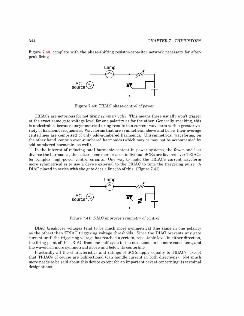
344 CHAPTER 7. THYRISTORS
Figure 7.40, complete with the phase-shifting resistor-capacitor network necessary for after-peak firing.
ACsource
Lamp
Figure 7.40: TRIAC phase-control of power
TRIACs are notorious for not firing symmetrically. This means these usually won’t triggerat the exact same gate voltage level for one polarity as for the other. Generally speaking, thisis undesirable, because unsymmetrical firing results in a current waveform with a greater va-riety of harmonic frequencies. Waveforms that are symmetrical above and below their averagecenterlines are comprised of only odd-numbered harmonics. Unsymmetrical waveforms, onthe other hand, contain even-numbered harmonics (which may or may not be accompanied byodd-numbered harmonics as well).
In the interest of reducing total harmonic content in power systems, the fewer and lessdiverse the harmonics, the better – one more reason individual SCRs are favored over TRIACsfor complex, high-power control circuits. One way to make the TRIAC’s current waveformmore symmetrical is to use a device external to the TRIAC to time the triggering pulse. ADIAC placed in series with the gate does a fair job of this: (Figure 7.41)
ACsource
Lamp
Figure 7.41: DIAC improves symmetry of control
DIAC breakover voltages tend to be much more symmetrical (the same in one polarityas the other) than TRIAC triggering voltage thresholds. Since the DIAC prevents any gatecurrent until the triggering voltage has reached a certain, repeatable level in either direction,the firing point of the TRIAC from one half-cycle to the next tends to be more consistent, andthe waveform more symmetrical above and below its centerline.
Practically all the characteristics and ratings of SCRs apply equally to TRIACs, exceptthat TRIACs of course are bidirectional (can handle current in both directions). Not muchmore needs to be said about this device except for an important caveat concerning its terminaldesignations.
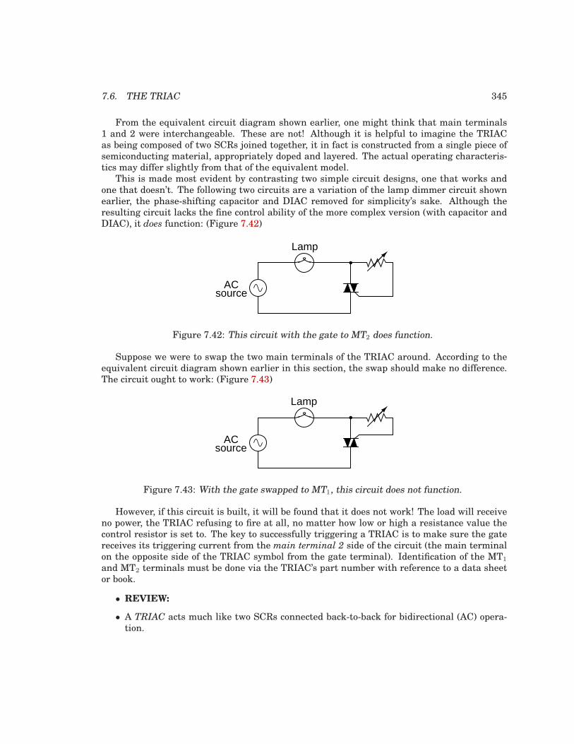
7.6. THE TRIAC 345
From the equivalent circuit diagram shown earlier, one might think that main terminals1 and 2 were interchangeable. These are not! Although it is helpful to imagine the TRIACas being composed of two SCRs joined together, it in fact is constructed from a single piece ofsemiconducting material, appropriately doped and layered. The actual operating characteris-tics may differ slightly from that of the equivalent model.
This is made most evident by contrasting two simple circuit designs, one that works andone that doesn’t. The following two circuits are a variation of the lamp dimmer circuit shownearlier, the phase-shifting capacitor and DIAC removed for simplicity’s sake. Although theresulting circuit lacks the fine control ability of the more complex version (with capacitor andDIAC), it does function: (Figure 7.42)
ACsource
Lamp
Figure 7.42: This circuit with the gate to MT2 does function.
Suppose we were to swap the two main terminals of the TRIAC around. According to theequivalent circuit diagram shown earlier in this section, the swap should make no difference.The circuit ought to work: (Figure 7.43)
ACsource
Lamp
Figure 7.43: With the gate swapped to MT1, this circuit does not function.
However, if this circuit is built, it will be found that it does not work! The load will receiveno power, the TRIAC refusing to fire at all, no matter how low or high a resistance value thecontrol resistor is set to. The key to successfully triggering a TRIAC is to make sure the gatereceives its triggering current from the main terminal 2 side of the circuit (the main terminalon the opposite side of the TRIAC symbol from the gate terminal). Identification of the MT1
and MT2 terminals must be done via the TRIAC’s part number with reference to a data sheetor book.
• REVIEW:
• A TRIAC acts much like two SCRs connected back-to-back for bidirectional (AC) opera-tion.
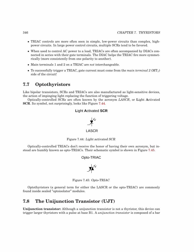
346 CHAPTER 7. THYRISTORS
• TRIAC controls are more often seen in simple, low-power circuits than complex, high-power circuits. In large power control circuits, multiple SCRs tend to be favored.
• When used to control AC power to a load, TRIACs are often accompanied by DIACs con-nected in series with their gate terminals. The DIAC helps the TRIAC fire more symmet-rically (more consistently from one polarity to another).
• Main terminals 1 and 2 on a TRIAC are not interchangeable.
• To successfully trigger a TRIAC, gate current must come from the main terminal 2 (MT2)side of the circuit!
7.7 Optothyristors
Like bipolar transistors, SCRs and TRIACs are also manufactured as light-sensitive devices,the action of impinging light replacing the function of triggering voltage.
Optically-controlled SCRs are often known by the acronym LASCR, or Light ActivatedSCR. Its symbol, not surprisingly, looks like Figure 7.44.
Light Activated SCR
LASCR
Figure 7.44: Light activated SCR
Optically-controlled TRIACs don’t receive the honor of having their own acronym, but in-stead are humbly known as opto-TRIACs. Their schematic symbol is shown in Figure 7.45.
Opto-TRIAC
Figure 7.45: Opto-TRIAC
Optothyristors (a general term for either the LASCR or the opto-TRIAC) are commonlyfound inside sealed ”optoisolator” modules.
7.8 The Unijunction Transistor (UJT)
Unijunction transistor: Although a unijunction transistor is not a thyristor, this device cantrigger larger thyristors with a pulse at base B1. A unijunction transistor is composed of a bar
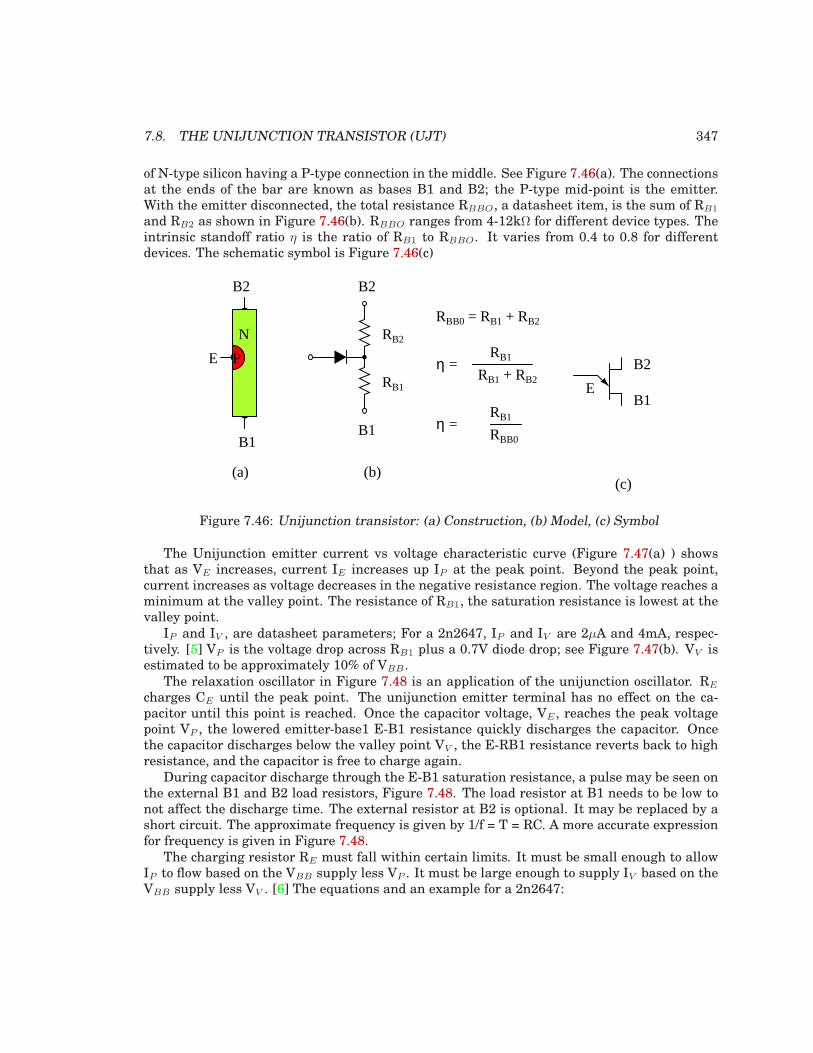
7.8. THE UNIJUNCTION TRANSISTOR (UJT) 347
of N-type silicon having a P-type connection in the middle. See Figure 7.46(a). The connectionsat the ends of the bar are known as bases B1 and B2; the P-type mid-point is the emitter.With the emitter disconnected, the total resistance RBBO, a datasheet item, is the sum of RB1
and RB2 as shown in Figure 7.46(b). RBBO ranges from 4-12kΩ for different device types. Theintrinsic standoff ratio η is the ratio of RB1 to RBBO. It varies from 0.4 to 0.8 for differentdevices. The schematic symbol is Figure 7.46(c)
B1
B2
E
P
B2
B1
E
(b)(a)
N
B2
B1
(c)
RB1
RB2
RBB0 = RB1 + RB2
η =RB1
RB1 + RB2
η =RB1
RBB0
Figure 7.46: Unijunction transistor: (a) Construction, (b) Model, (c) Symbol
The Unijunction emitter current vs voltage characteristic curve (Figure 7.47(a) ) showsthat as VE increases, current IE increases up IP at the peak point. Beyond the peak point,current increases as voltage decreases in the negative resistance region. The voltage reaches aminimum at the valley point. The resistance of RB1, the saturation resistance is lowest at thevalley point.
IP and IV , are datasheet parameters; For a 2n2647, IP and IV are 2µA and 4mA, respec-tively. [5] VP is the voltage drop across RB1 plus a 0.7V diode drop; see Figure 7.47(b). VV isestimated to be approximately 10% of VBB .
The relaxation oscillator in Figure 7.48 is an application of the unijunction oscillator. RE
charges CE until the peak point. The unijunction emitter terminal has no effect on the ca-pacitor until this point is reached. Once the capacitor voltage, VE , reaches the peak voltagepoint VP , the lowered emitter-base1 E-B1 resistance quickly discharges the capacitor. Oncethe capacitor discharges below the valley point VV , the E-RB1 resistance reverts back to highresistance, and the capacitor is free to charge again.
During capacitor discharge through the E-B1 saturation resistance, a pulse may be seen onthe external B1 and B2 load resistors, Figure 7.48. The load resistor at B1 needs to be low tonot affect the discharge time. The external resistor at B2 is optional. It may be replaced by ashort circuit. The approximate frequency is given by 1/f = T = RC. A more accurate expressionfor frequency is given in Figure 7.48.
The charging resistor RE must fall within certain limits. It must be small enough to allowIP to flow based on the VBB supply less VP . It must be large enough to supply IV based on theVBB supply less VV . [6] The equations and an example for a 2n2647:
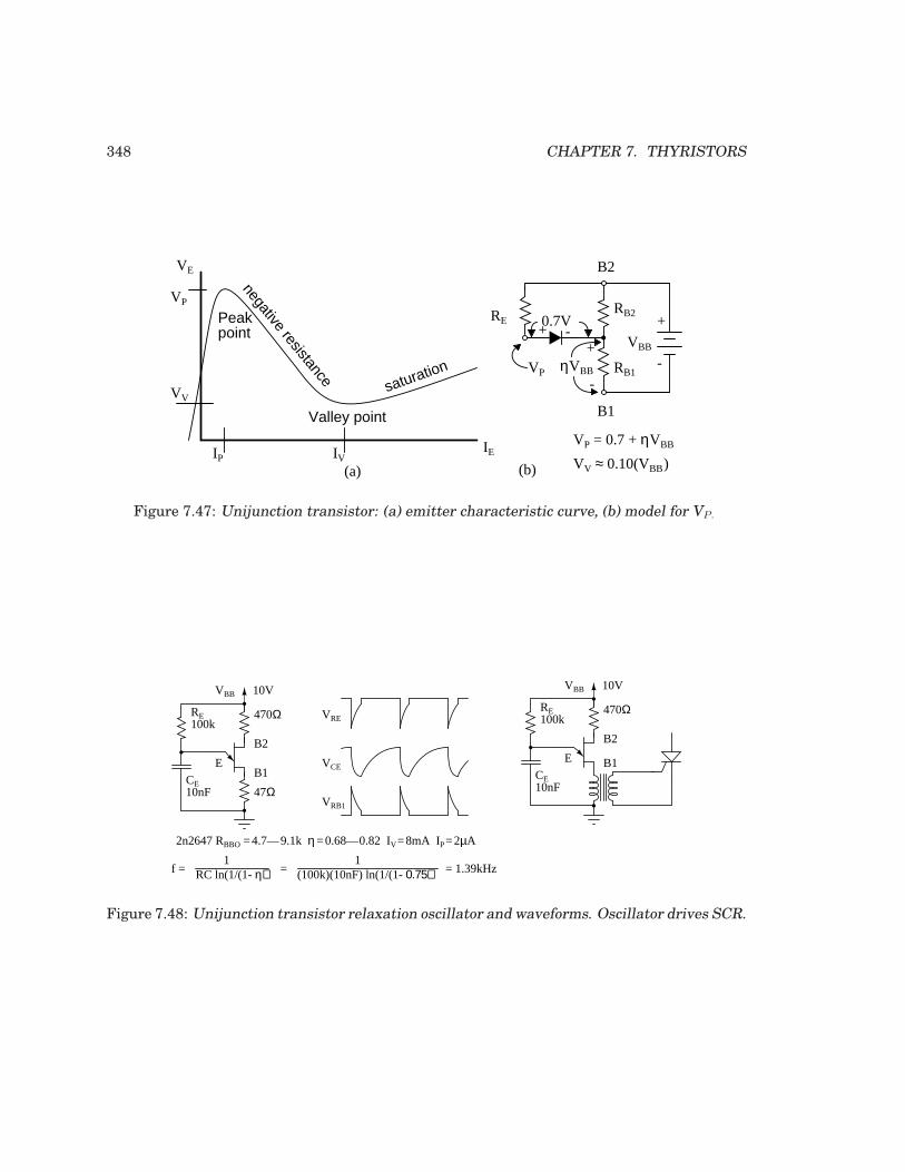
348 CHAPTER 7. THYRISTORS
IE
Valley point
Peakpoint
negative resistance
saturation
(a)
VP
IP IV
VV
B2
B1
RB1
RB20.7V +
-+
-
+ -
ηVBB
VBB
RE
VP = 0.7 + ηVBB
VV ≈ 0.10(VBB)
VP
(b)
VE
Figure 7.47: Unijunction transistor: (a) emitter characteristic curve, (b) model for VP.
f = 1
RC ln(1/(1- η))
2n2647 RBBO = 4.7—9.1k η = 0.68—0.82 IV=8mA IP= 2µA
RE100k
CE10nF
=1
(100k)(10nF) ln(1/(1- 0.75)) = 1.39kHz
B1
B2
E
VRE
VRB1
VCE
VBB 10V
470Ω
47Ω
RE100k
CE10nF
B1
B2
E
VBB 10V
470Ω
Figure 7.48: Unijunction transistor relaxation oscillator and waveforms. Oscillator drives SCR.
7.8. THE UNIJUNCTION TRANSISTOR (UJT) 349
2n2647 RBBO =4.7— 9.1k η =0.68—0.82 IV= 8mA IP=2µA
IP
VBB - VP
IV
VBB - VV < RE <2µA
10 - 8.2
8mA
10 - 1< RE <
VP = 0.7 + ηVBBVP = 0.7 + 0.75(10) = 8.2V
VV = 0.10(VBB) VV = 0.10(10) = 1V
< RE < 900k1.125k
Programmable Unijunction Transistor (PUT): Although the unijunction transistor islisted as obsolete (read expensive if obtainable), the programmable unijunction transistor isalive and well. It is inexpensive and in production. Though it serves a function similar to theunijunction transistor, the PUT is a three terminal thyristor. The PUT shares the four-layerstructure typical of thyristors shown in Figure 7.49. Note that the gate, an N-type layer nearthe anode, is known as an “anode gate”. Moreover, the gate lead on the schematic symbol isattached to the anode end of the symbol.
A
K
G
VA
IA
G
P
N
P
N
A
K
VP
VV
IP IV
Figure 7.49: Programmable unijunction transistor: Characteristic curve, internal construction,schematic symbol.
The characteristic curve for the programmable unijunction transistor in Figure 7.49 is sim-ilar to that of the unijunction transistor. This is a plot of anode current IA versus anodevoltage VA. The gate lead voltage sets, programs, the peak anode voltage VP . As anode cur-rent inceases, voltage increases up to the peak point. Thereafter, increasing current results indecreasing voltage, down to the valley point.
The PUT equivalent of the unijunction transistor is shown in Figure 7.50. External PUTresistors R1 and R2 replace unijunction transistor internal resistors RB1 and RB2, respectively.These resistors allow the calculation of the intrinsic standoff ratio η.
Figure 7.51 shows the PUT version of the unijunction relaxation oscillator Figure 7.48.Resistor R charges the capacitor until the peak point, Figure 7.49, then heavy conductionmoves the operating point down the negative resistance slope to the valley point. A currentspike flows through the cathode during capacitor discharge, developing a voltage spike acrossthe cathode resistors. After capacitor discharge, the operating point resets back to the slope up
350 CHAPTER 7. THYRISTORS
A
K
G
B1
B2
E
R1
R2
B1
B2
E
RBB0 = R1 + R2
η =R1
R1 + R2
Unijunction PUT equivalentRG =
R1 + R2R1⋅R2
VS = ηVBB
VS
VP = VT + VS
Figure 7.50: PUT equivalent of unijunction transistor
to the peak point.
R
C
VRK
VC
VBB 10V
47Ω
K
A G VG VP
0VR1
R2
VRK
Figure 7.51: PUT relaxation oscillator
Problem: What is the range of suitable values for R in Figure 7.51, a relaxation oscillator?The charging resistor must be small enough to supply enough current to raise the anode to VP
the peak point (Figure 7.49) while charging the capacitor. Once VP is reached, anode voltagedecreases as current increases (negative resistance), which moves the operating point to thevalley. It is the job of the capacitor to supply the valley current IV . Once it is discharged,the operating point resets back to the upward slope to the peak point. The resistor must belarge enough so that it will never supply the high valley current IP . If the charging resistorever could supply that much current, the resistor would supply the valley current after thecapacitor was discharged and the operating point would never reset back to the high resistancecondition to the left of the peak point.
We select the same VBB=10V used for the unijunction transistor example. We select valuesof R1 and R2 so that η is about 2/3. We calculate η and VS . The parallel equivalent of R1, R2 isRG, which is only used to make selections from Table 7.1. Along with VS=10, the closest value
7.8. THE UNIJUNCTION TRANSISTOR (UJT) 351
to our 6.3, we find VT=0.6V, in Table 7.1 and calculate VP .
η =R1
R1 + R2
RG = R1 + R2R1⋅R2
VS = ηVBB
VP = VT + VS
R1 = 27k R2 = 16k
η =27
27 + 16 = 0.6279
VBB = 10V
VS = 0.6279(10) = 6.279V
VP = 0.6 + 6.3 = 6.9V
RG = 27k + 16k27k⋅16k
= 10k
For RG=10k and VS=10V, VT = 0.6V
We also find IP and IV , the peak and valley currents, respectively in Table 7.1. We still needVV , the valley voltage. We used 10% of VBB= 1V, in the previous unijunction example. Con-sulting the datasheet, we find the forward voltage VF=0.8V at IF=50mA. The valley currentIV =70µA is much less than IF=50mA. Therefore, VV must be less than VF=0.8V. How muchless? To be safe we set VV =0V. This will raise the lower limit on the resistor range a little.
IP
VBB - VP
IV
VBB - VV < RE <4µA
10 - 6.9
70µA
10 - 0< RE <
VV = 0.10(VBB) not used VV = 0V
< RE < 755k143k
For RG=10k and VS=10V, IV = 70µA
For RG=10k and VS=10V, IP = 4.0µA
Choosing R > 143k guarantees that the operating point can reset from the valley point aftercapacitor discharge. R < 755k allows charging up to VP at the peak point.
Table 7.1: Selected 2n6027 PUT parameters, adapted from 2n6027 datasheet. [4]Parameter Conditions min typical max units
VT VVS=10V, RG=1Meg 0.2 0.7 1.6VS=10V, RG=10k 0.2 0.35 0.6
IP µAVS=10V, RG=1Meg - 1.25 2.0VS=10V, RG=10k - 4.0 5.0
IV µAVS=10V, RG=1Meg - 18 50VS=10V, RG=10k 70 150 -VS=10V, RG=200Ω 1500 - -
VF IF=50mA - 0.8 1.5 V
Figure 7.52 show the PUT relaxation oscillator with the final resistor values. A practical
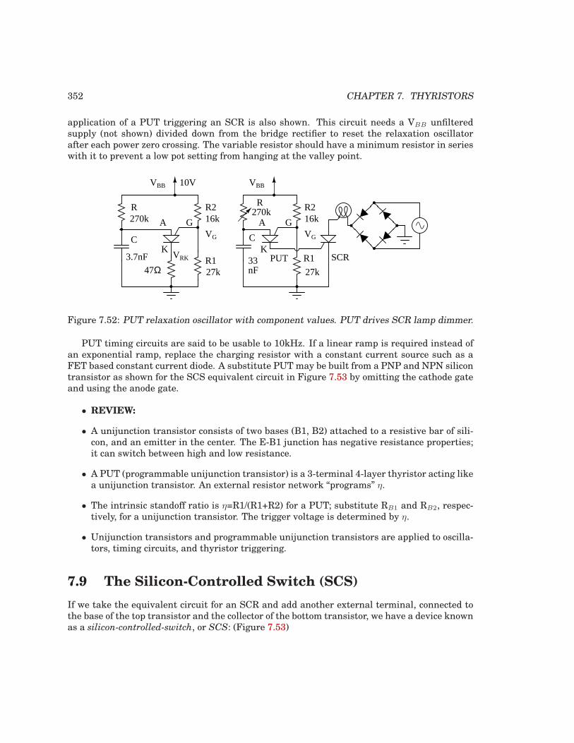
352 CHAPTER 7. THYRISTORS
application of a PUT triggering an SCR is also shown. This circuit needs a VBB unfilteredsupply (not shown) divided down from the bridge rectifier to reset the relaxation oscillatorafter each power zero crossing. The variable resistor should have a minimum resistor in serieswith it to prevent a low pot setting from hanging at the valley point.
R
C
VBB 10V
47Ω
K
A GVG
R1
R2
VRK
27k
16k270k
3.7nF
R
C
VBB
K
A GVG
R1
R2
27k
16k
SCRPUT33nF
270k
Figure 7.52: PUT relaxation oscillator with component values. PUT drives SCR lamp dimmer.
PUT timing circuits are said to be usable to 10kHz. If a linear ramp is required instead ofan exponential ramp, replace the charging resistor with a constant current source such as aFET based constant current diode. A substitute PUT may be built from a PNP and NPN silicontransistor as shown for the SCS equivalent circuit in Figure 7.53 by omitting the cathode gateand using the anode gate.
• REVIEW:
• A unijunction transistor consists of two bases (B1, B2) attached to a resistive bar of sili-con, and an emitter in the center. The E-B1 junction has negative resistance properties;it can switch between high and low resistance.
• A PUT (programmable unijunction transistor) is a 3-terminal 4-layer thyristor acting likea unijunction transistor. An external resistor network “programs” η.
• The intrinsic standoff ratio is η=R1/(R1+R2) for a PUT; substitute RB1 and RB2, respec-tively, for a unijunction transistor. The trigger voltage is determined by η.
• Unijunction transistors and programmable unijunction transistors are applied to oscilla-tors, timing circuits, and thyristor triggering.
7.9 The Silicon-Controlled Switch (SCS)
If we take the equivalent circuit for an SCR and add another external terminal, connected tothe base of the top transistor and the collector of the bottom transistor, we have a device knownas a silicon-controlled-switch, or SCS: (Figure 7.53)
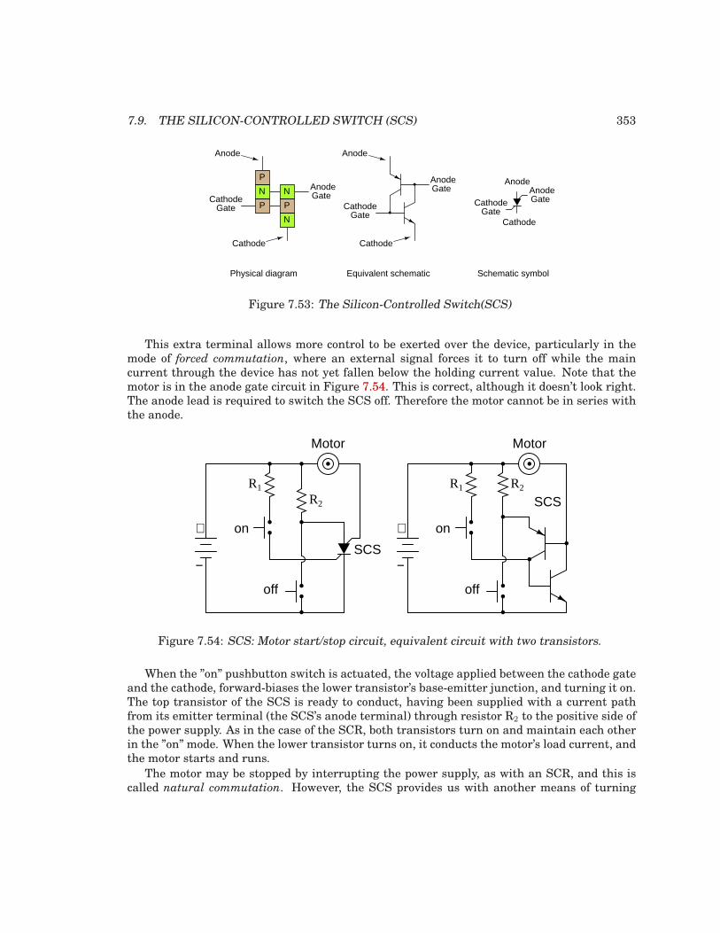
7.9. THE SILICON-CONTROLLED SWITCH (SCS) 353
Anode
Cathode Cathode
Anode
Physical diagram Equivalent schematic Schematic symbol
Gate
Cathode
Anode
Cathode GateAnode
CathodeGate
AnodeGate
CathodeGate
AnodeGate
P
P
N
N
N
P
Figure 7.53: The Silicon-Controlled Switch(SCS)
This extra terminal allows more control to be exerted over the device, particularly in themode of forced commutation, where an external signal forces it to turn off while the maincurrent through the device has not yet fallen below the holding current value. Note that themotor is in the anode gate circuit in Figure 7.54. This is correct, although it doesn’t look right.The anode lead is required to switch the SCS off. Therefore the motor cannot be in series withthe anode.
on
off
Motor
R1
R2
on
off
Motor
R1 R2
SCS
SCS
+
−
+
−
Figure 7.54: SCS: Motor start/stop circuit, equivalent circuit with two transistors.
When the ”on” pushbutton switch is actuated, the voltage applied between the cathode gateand the cathode, forward-biases the lower transistor’s base-emitter junction, and turning it on.The top transistor of the SCS is ready to conduct, having been supplied with a current pathfrom its emitter terminal (the SCS’s anode terminal) through resistor R2 to the positive side ofthe power supply. As in the case of the SCR, both transistors turn on and maintain each otherin the ”on” mode. When the lower transistor turns on, it conducts the motor’s load current, andthe motor starts and runs.
The motor may be stopped by interrupting the power supply, as with an SCR, and this iscalled natural commutation. However, the SCS provides us with another means of turning
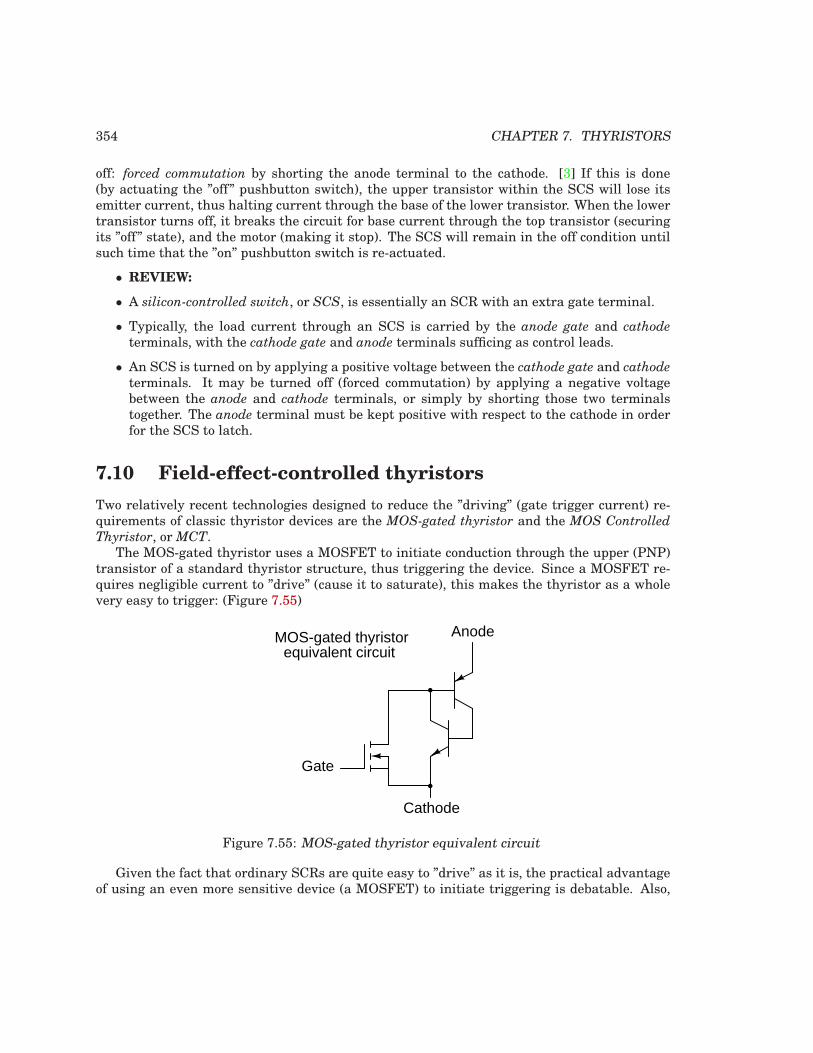
354 CHAPTER 7. THYRISTORS
off: forced commutation by shorting the anode terminal to the cathode. [3] If this is done(by actuating the ”off” pushbutton switch), the upper transistor within the SCS will lose itsemitter current, thus halting current through the base of the lower transistor. When the lowertransistor turns off, it breaks the circuit for base current through the top transistor (securingits ”off” state), and the motor (making it stop). The SCS will remain in the off condition untilsuch time that the ”on” pushbutton switch is re-actuated.
• REVIEW:
• A silicon-controlled switch, or SCS, is essentially an SCR with an extra gate terminal.
• Typically, the load current through an SCS is carried by the anode gate and cathode
terminals, with the cathode gate and anode terminals sufficing as control leads.
• An SCS is turned on by applying a positive voltage between the cathode gate and cathode
terminals. It may be turned off (forced commutation) by applying a negative voltagebetween the anode and cathode terminals, or simply by shorting those two terminalstogether. The anode terminal must be kept positive with respect to the cathode in orderfor the SCS to latch.
7.10 Field-effect-controlled thyristors
Two relatively recent technologies designed to reduce the ”driving” (gate trigger current) re-quirements of classic thyristor devices are the MOS-gated thyristor and the MOS Controlled
Thyristor, or MCT.The MOS-gated thyristor uses a MOSFET to initiate conduction through the upper (PNP)
transistor of a standard thyristor structure, thus triggering the device. Since a MOSFET re-quires negligible current to ”drive” (cause it to saturate), this makes the thyristor as a wholevery easy to trigger: (Figure 7.55)
Cathode
Anode
Gate
MOS-gated thyristorequivalent circuit
Figure 7.55: MOS-gated thyristor equivalent circuit
Given the fact that ordinary SCRs are quite easy to ”drive” as it is, the practical advantageof using an even more sensitive device (a MOSFET) to initiate triggering is debatable. Also,
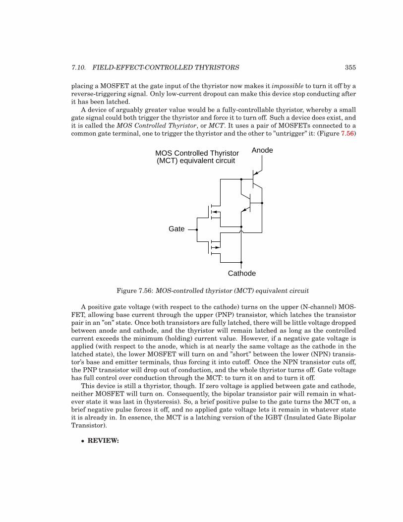
7.10. FIELD-EFFECT-CONTROLLED THYRISTORS 355
placing a MOSFET at the gate input of the thyristor now makes it impossible to turn it off by areverse-triggering signal. Only low-current dropout can make this device stop conducting afterit has been latched.
A device of arguably greater value would be a fully-controllable thyristor, whereby a smallgate signal could both trigger the thyristor and force it to turn off. Such a device does exist, andit is called the MOS Controlled Thyristor, or MCT. It uses a pair of MOSFETs connected to acommon gate terminal, one to trigger the thyristor and the other to ”untrigger” it: (Figure 7.56)
Cathode
Anode
Gate
MOS Controlled Thyristor(MCT) equivalent circuit
Figure 7.56: MOS-controlled thyristor (MCT) equivalent circuit
A positive gate voltage (with respect to the cathode) turns on the upper (N-channel) MOS-FET, allowing base current through the upper (PNP) transistor, which latches the transistorpair in an ”on” state. Once both transistors are fully latched, there will be little voltage droppedbetween anode and cathode, and the thyristor will remain latched as long as the controlledcurrent exceeds the minimum (holding) current value. However, if a negative gate voltage isapplied (with respect to the anode, which is at nearly the same voltage as the cathode in thelatched state), the lower MOSFET will turn on and ”short” between the lower (NPN) transis-tor’s base and emitter terminals, thus forcing it into cutoff. Once the NPN transistor cuts off,the PNP transistor will drop out of conduction, and the whole thyristor turns off. Gate voltagehas full control over conduction through the MCT: to turn it on and to turn it off.
This device is still a thyristor, though. If zero voltage is applied between gate and cathode,neither MOSFET will turn on. Consequently, the bipolar transistor pair will remain in what-ever state it was last in (hysteresis). So, a brief positive pulse to the gate turns the MCT on, abrief negative pulse forces it off, and no applied gate voltage lets it remain in whatever stateit is already in. In essence, the MCT is a latching version of the IGBT (Insulated Gate BipolarTransistor).
• REVIEW:
356 CHAPTER 7. THYRISTORS
• A MOS-gated thyristor uses an N-channel MOSFET to trigger a thyristor, resulting in anextremely low gate current requirement.
• A MOS Controlled Thyristor, or MCT, uses two MOSFETS to exert full control over thethyristor. A positive gate voltage triggers the device; a negative gate voltage forces itto turn off. Zero gate voltage allows the thyristor to remain in whatever state it waspreviously in (off, or latched on).
Bibliography
[1] “Phattytron PT-1 Vacuum Tube Synthesizer”, The Audio Playground Synthesizer Mu-seum at http://www.keyboardmuseum.com/ar/m/meta/pt1.html
[2] “At last, a pitch source with tube power”, METASONIX, PMB 109, 88111th Street, Lakeport CA 95453 USA at http://www.metasonix.com/index.php?option=com content&task=view&id=14&Itemid=31
[3] “Silicon Contolled Switches”, GE Transistor Manual, The General Electric Company,1964, Figure 16.19(M).
[4] “2N6027, 2N6028 Programmable Unijunction Transistor ”, datasheet athttp://www.onsemi.com/pub link/Collateral/2N6027-D.PDF
[5] “Unijunction Transistor ”, American Microsemiconductor, athttp://www.americanmicrosemi.com/tutorials/unijunct ion.htm
[6] Matthew H. Williams, “Unijunction Transistor ”, athttp://baec.tripod.com/DEC90/uni tran.htm Unijunction Transistor byhttp://baec.tripod.com/DEC90/uni tran.htm
Chapter 8
OPERATIONAL AMPLIFIERS
Contents
8.1 Introduction . . . . . . . . . . . . . . . . . . . . . . . . . . . . . . . . . . . . . . 357
8.2 Single-ended and differential amplifiers . . . . . . . . . . . . . . . . . . . . 358
8.3 The ”operational” amplifier . . . . . . . . . . . . . . . . . . . . . . . . . . . . 362
8.4 Negative feedback . . . . . . . . . . . . . . . . . . . . . . . . . . . . . . . . . . 368
8.5 Divided feedback . . . . . . . . . . . . . . . . . . . . . . . . . . . . . . . . . . . 371
8.6 An analogy for divided feedback . . . . . . . . . . . . . . . . . . . . . . . . . 374
8.7 Voltage-to-current signal conversion . . . . . . . . . . . . . . . . . . . . . . 380
8.8 Averager and summer circuits . . . . . . . . . . . . . . . . . . . . . . . . . . 382
8.9 Building a differential amplifier . . . . . . . . . . . . . . . . . . . . . . . . . 384
8.10 The instrumentation amplifier . . . . . . . . . . . . . . . . . . . . . . . . . . 386
8.11 Differentiator and integrator circuits . . . . . . . . . . . . . . . . . . . . . . 387
8.12 Positive feedback . . . . . . . . . . . . . . . . . . . . . . . . . . . . . . . . . . . 390
8.13 Practical considerations . . . . . . . . . . . . . . . . . . . . . . . . . . . . . . 394
8.13.1 Common-mode gain . . . . . . . . . . . . . . . . . . . . . . . . . . . . . . . 395
8.13.2 Offset voltage . . . . . . . . . . . . . . . . . . . . . . . . . . . . . . . . . . 398
8.13.3 Bias current . . . . . . . . . . . . . . . . . . . . . . . . . . . . . . . . . . . 400
8.13.4 Drift . . . . . . . . . . . . . . . . . . . . . . . . . . . . . . . . . . . . . . . 406
8.13.5 Frequency response . . . . . . . . . . . . . . . . . . . . . . . . . . . . . . . 406
8.13.6 Input to output phase shift . . . . . . . . . . . . . . . . . . . . . . . . . . . 407
8.14 Operational amplifier models . . . . . . . . . . . . . . . . . . . . . . . . . . . 410
8.15 Data . . . . . . . . . . . . . . . . . . . . . . . . . . . . . . . . . . . . . . . . . . . 415
8.1 Introduction
The operational amplifier is arguably the most useful single device in analog electronic cir-cuitry. With only a handful of external components, it can be made to perform a wide variety
357
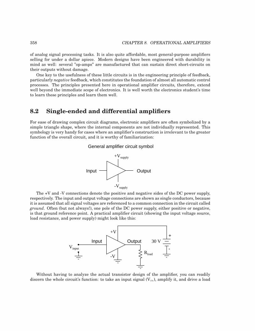
358 CHAPTER 8. OPERATIONAL AMPLIFIERS
of analog signal processing tasks. It is also quite affordable, most general-purpose amplifiersselling for under a dollar apiece. Modern designs have been engineered with durability inmind as well: several ”op-amps” are manufactured that can sustain direct short-circuits ontheir outputs without damage.
One key to the usefulness of these little circuits is in the engineering principle of feedback,particularly negative feedback, which constitutes the foundation of almost all automatic controlprocesses. The principles presented here in operational amplifier circuits, therefore, extendwell beyond the immediate scope of electronics. It is well worth the electronics student’s timeto learn these principles and learn them well.
8.2 Single-ended and differential amplifiers
For ease of drawing complex circuit diagrams, electronic amplifiers are often symbolized by asimple triangle shape, where the internal components are not individually represented. Thissymbology is very handy for cases where an amplifier’s construction is irrelevant to the greaterfunction of the overall circuit, and it is worthy of familiarization:
Input Output
+Vsupply
-Vsupply
General amplifier circuit symbol
The +V and -V connections denote the positive and negative sides of the DC power supply,respectively. The input and output voltage connections are shown as single conductors, becauseit is assumed that all signal voltages are referenced to a common connection in the circuit calledground. Often (but not always!), one pole of the DC power supply, either positive or negative,is that ground reference point. A practical amplifier circuit (showing the input voltage source,load resistance, and power supply) might look like this:
Rload
Vinput
Input Output
+V
-V
30 V+
-
Without having to analyze the actual transistor design of the amplifier, you can readilydiscern the whole circuit’s function: to take an input signal (Vin), amplify it, and drive a load
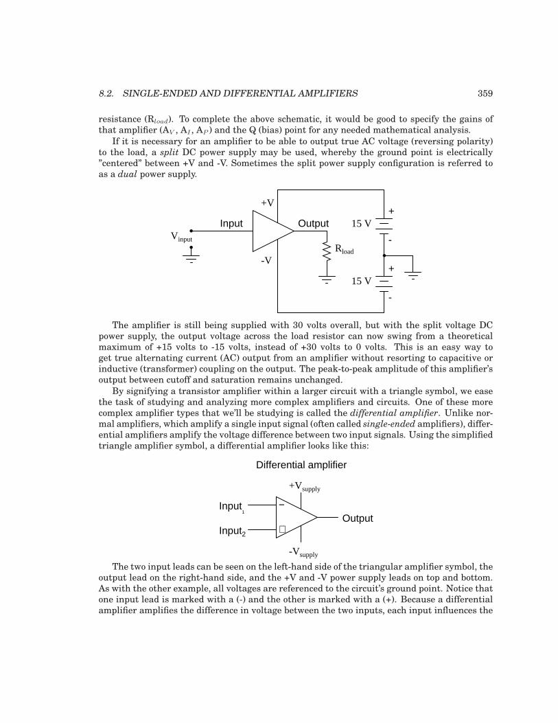
8.2. SINGLE-ENDED AND DIFFERENTIAL AMPLIFIERS 359
resistance (Rload). To complete the above schematic, it would be good to specify the gains ofthat amplifier (AV , AI , AP ) and the Q (bias) point for any needed mathematical analysis.
If it is necessary for an amplifier to be able to output true AC voltage (reversing polarity)to the load, a split DC power supply may be used, whereby the ground point is electrically”centered” between +V and -V. Sometimes the split power supply configuration is referred toas a dual power supply.
Rload
Vinput
Input Output
+V
-V
+
-
+
-
15 V
15 V
The amplifier is still being supplied with 30 volts overall, but with the split voltage DCpower supply, the output voltage across the load resistor can now swing from a theoreticalmaximum of +15 volts to -15 volts, instead of +30 volts to 0 volts. This is an easy way toget true alternating current (AC) output from an amplifier without resorting to capacitive orinductive (transformer) coupling on the output. The peak-to-peak amplitude of this amplifier’soutput between cutoff and saturation remains unchanged.
By signifying a transistor amplifier within a larger circuit with a triangle symbol, we easethe task of studying and analyzing more complex amplifiers and circuits. One of these morecomplex amplifier types that we’ll be studying is called the differential amplifier. Unlike nor-mal amplifiers, which amplify a single input signal (often called single-ended amplifiers), differ-ential amplifiers amplify the voltage difference between two input signals. Using the simplifiedtriangle amplifier symbol, a differential amplifier looks like this:
−
+
Input1
Input2
+Vsupply
-Vsupply
Output
Differential amplifier
The two input leads can be seen on the left-hand side of the triangular amplifier symbol, theoutput lead on the right-hand side, and the +V and -V power supply leads on top and bottom.As with the other example, all voltages are referenced to the circuit’s ground point. Notice thatone input lead is marked with a (-) and the other is marked with a (+). Because a differentialamplifier amplifies the difference in voltage between the two inputs, each input influences the
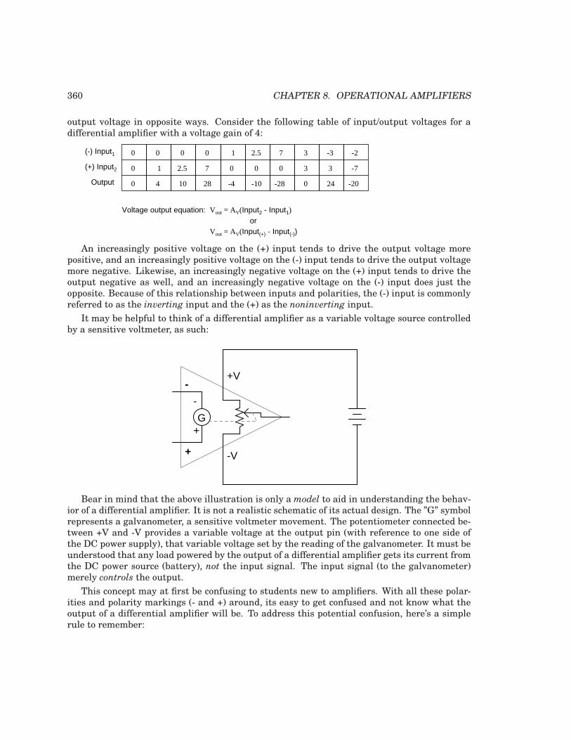
360 CHAPTER 8. OPERATIONAL AMPLIFIERS
output voltage in opposite ways. Consider the following table of input/output voltages for adifferential amplifier with a voltage gain of 4:
Output
(-) Input1
(+) Input2
0
0
0
0 0 0 1 2.5 7
0 0 01 2.5 7
4 10 28 -4 -10 -28
3
3
-3
3
0 24
-2
-7
-20
Voltage output equation: Vout = AV(Input2 - Input1)
orVout = AV(Input(+) - Input(-))
An increasingly positive voltage on the (+) input tends to drive the output voltage morepositive, and an increasingly positive voltage on the (-) input tends to drive the output voltagemore negative. Likewise, an increasingly negative voltage on the (+) input tends to drive theoutput negative as well, and an increasingly negative voltage on the (-) input does just theopposite. Because of this relationship between inputs and polarities, the (-) input is commonlyreferred to as the inverting input and the (+) as the noninverting input.
It may be helpful to think of a differential amplifier as a variable voltage source controlledby a sensitive voltmeter, as such:
G
-
+
+V
-V
-
+
Bear in mind that the above illustration is only a model to aid in understanding the behav-ior of a differential amplifier. It is not a realistic schematic of its actual design. The ”G” symbolrepresents a galvanometer, a sensitive voltmeter movement. The potentiometer connected be-tween +V and -V provides a variable voltage at the output pin (with reference to one side ofthe DC power supply), that variable voltage set by the reading of the galvanometer. It must beunderstood that any load powered by the output of a differential amplifier gets its current fromthe DC power source (battery), not the input signal. The input signal (to the galvanometer)merely controls the output.
This concept may at first be confusing to students new to amplifiers. With all these polar-ities and polarity markings (- and +) around, its easy to get confused and not know what theoutput of a differential amplifier will be. To address this potential confusion, here’s a simplerule to remember:
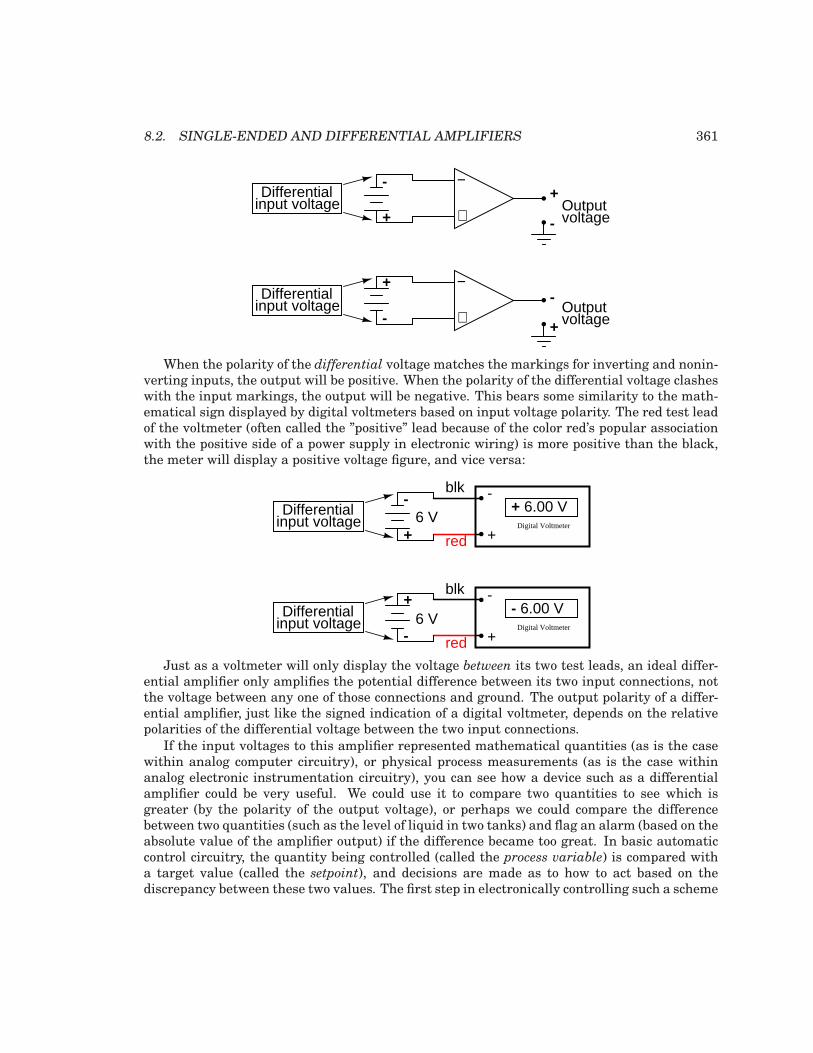
8.2. SINGLE-ENDED AND DIFFERENTIAL AMPLIFIERS 361
−
+Differential
input voltage
-
+
+
-Outputvoltage
Differentialinput voltage
-
+ −
++
-voltageOutput
When the polarity of the differential voltage matches the markings for inverting and nonin-verting inputs, the output will be positive. When the polarity of the differential voltage clasheswith the input markings, the output will be negative. This bears some similarity to the math-ematical sign displayed by digital voltmeters based on input voltage polarity. The red test leadof the voltmeter (often called the ”positive” lead because of the color red’s popular associationwith the positive side of a power supply in electronic wiring) is more positive than the black,the meter will display a positive voltage figure, and vice versa:
Differentialinput voltage
-
+
Differentialinput voltage
-
+
6 V
6 V
-
+
-
+red
blk
blk
red
Digital Voltmeter
Digital Voltmeter
+ 6.00 V
- 6.00 V
Just as a voltmeter will only display the voltage between its two test leads, an ideal differ-ential amplifier only amplifies the potential difference between its two input connections, notthe voltage between any one of those connections and ground. The output polarity of a differ-ential amplifier, just like the signed indication of a digital voltmeter, depends on the relativepolarities of the differential voltage between the two input connections.
If the input voltages to this amplifier represented mathematical quantities (as is the casewithin analog computer circuitry), or physical process measurements (as is the case withinanalog electronic instrumentation circuitry), you can see how a device such as a differentialamplifier could be very useful. We could use it to compare two quantities to see which isgreater (by the polarity of the output voltage), or perhaps we could compare the differencebetween two quantities (such as the level of liquid in two tanks) and flag an alarm (based on theabsolute value of the amplifier output) if the difference became too great. In basic automaticcontrol circuitry, the quantity being controlled (called the process variable) is compared witha target value (called the setpoint), and decisions are made as to how to act based on thediscrepancy between these two values. The first step in electronically controlling such a scheme
362 CHAPTER 8. OPERATIONAL AMPLIFIERS
is to amplify the difference between the process variable and the setpoint with a differentialamplifier. In simple controller designs, the output of this differential amplifier can be directlyutilized to drive the final control element (such as a valve) and keep the process reasonablyclose to setpoint.
• REVIEW:
• A ”shorthand” symbol for an electronic amplifier is a triangle, the wide end signifyingthe input side and the narrow end signifying the output. Power supply lines are oftenomitted in the drawing for simplicity.
• To facilitate true AC output from an amplifier, we can use what is called a split or dual
power supply, with two DC voltage sources connected in series with the middle pointgrounded, giving a positive voltage to ground (+V) and a negative voltage to ground (-V).Split power supplies like this are frequently used in differential amplifier circuits.
• Most amplifiers have one input and one output. Differential amplifiers have two inputsand one output, the output signal being proportional to the difference in signals betweenthe two inputs.
• The voltage output of a differential amplifier is determined by the following equation:Vout = AV (Vnoninv - Vinv)
8.3 The ”operational” amplifier
Long before the advent of digital electronic technology, computers were built to electronicallyperform calculations by employing voltages and currents to represent numerical quantities.This was especially useful for the simulation of physical processes. A variable voltage, for in-stance, might represent velocity or force in a physical system. Through the use of resistivevoltage dividers and voltage amplifiers, the mathematical operations of division and multipli-cation could be easily performed on these signals.
The reactive properties of capacitors and inductors lend themselves well to the simulationof variables related by calculus functions. Remember how the current through a capacitorwas a function of the voltage’s rate of change, and how that rate of change was designatedin calculus as the derivative? Well, if voltage across a capacitor were made to represent thevelocity of an object, the current through the capacitor would represent the force required toaccelerate or decelerate that object, the capacitor’s capacitance representing the object’s mass:
iC = C dvdt
F = m dvdt
Where, Where,
iC =
C =
dvdt
=
Instantaneous current through capacitorCapacitance in farads
Rate of change of voltage over time
F =
m =
dvdt
=
Force applied to object
Mass of object
Rate of change of velocity over time
8.3. THE ”OPERATIONAL” AMPLIFIER 363
This analog electronic computation of the calculus derivative function is technically knownas differentiation, and it is a natural function of a capacitor’s current in relation to the voltageapplied across it. Note that this circuit requires no ”programming” to perform this relativelyadvanced mathematical function as a digital computer would.
Electronic circuits are very easy and inexpensive to create compared to complex physicalsystems, so this kind of analog electronic simulation was widely used in the research anddevelopment of mechanical systems. For realistic simulation, though, amplifier circuits of highaccuracy and easy configurability were needed in these early computers.
It was found in the course of analog computer design that differential amplifiers with ex-tremely high voltage gains met these requirements of accuracy and configurability better thansingle-ended amplifiers with custom-designed gains. Using simple components connected tothe inputs and output of the high-gain differential amplifier, virtually any gain and any func-tion could be obtained from the circuit, overall, without adjusting or modifying the internalcircuitry of the amplifier itself. These high-gain differential amplifiers came to be known asoperational amplifiers, or op-amps, because of their application in analog computers’ mathe-matical operations.
Modern op-amps, like the popular model 741, are high-performance, inexpensive integratedcircuits. Their input impedances are quite high, the inputs drawing currents in the range ofhalf a microamp (maximum) for the 741, and far less for op-amps utilizing field-effect inputtransistors. Output impedance is typically quite low, about 75 Ω for the model 741, and manymodels have built-in output short circuit protection, meaning that their outputs can be directlyshorted to ground without causing harm to the internal circuitry. With direct coupling betweenop-amps’ internal transistor stages, they can amplify DC signals just as well as AC (up tocertain maximum voltage-risetime limits). It would cost far more in money and time to designa comparable discrete-transistor amplifier circuit to match that kind of performance, unlesshigh power capability was required. For these reasons, op-amps have all but obsoleted discrete-transistor signal amplifiers in many applications.
The following diagram shows the pin connections for single op-amps (741 included) whenhoused in an 8-pin DIP (Dual Inline Package) integrated circuit:
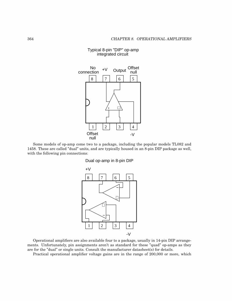
364 CHAPTER 8. OPERATIONAL AMPLIFIERS
Typical 8-pin "DIP" op-ampintegrated circuit
8 7 6
1 2 3 4
5
− +
+V
-V
OutputNo
connectionOffset
null
Offsetnull
Some models of op-amp come two to a package, including the popular models TL082 and1458. These are called ”dual” units, and are typically housed in an 8-pin DIP package as well,with the following pin connections:
8 7 6
1 2 3 4
5
Dual op-amp in 8-pin DIP
+V
-V
−
+
−
+
Operational amplifiers are also available four to a package, usually in 14-pin DIP arrange-ments. Unfortunately, pin assignments aren’t as standard for these ”quad” op-amps as theyare for the ”dual” or single units. Consult the manufacturer datasheet(s) for details.
Practical operational amplifier voltage gains are in the range of 200,000 or more, which
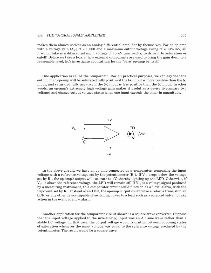
8.3. THE ”OPERATIONAL” AMPLIFIER 365
makes them almost useless as an analog differential amplifier by themselves. For an op-ampwith a voltage gain (AV ) of 200,000 and a maximum output voltage swing of +15V/-15V, allit would take is a differential input voltage of 75 µV (microvolts) to drive it to saturation orcutoff! Before we take a look at how external components are used to bring the gain down to areasonable level, let’s investigate applications for the ”bare” op-amp by itself.
One application is called the comparator. For all practical purposes, we can say that theoutput of an op-amp will be saturated fully positive if the (+) input is more positive than the (-)input, and saturated fully negative if the (+) input is less positive than the (-) input. In otherwords, an op-amp’s extremely high voltage gain makes it useful as a device to compare twovoltages and change output voltage states when one input exceeds the other in magnitude.
−
+
+V
-V
LEDVin
In the above circuit, we have an op-amp connected as a comparator, comparing the inputvoltage with a reference voltage set by the potentiometer (R1). If Vin drops below the voltageset by R1, the op-amp’s output will saturate to +V, thereby lighting up the LED. Otherwise, ifVin is above the reference voltage, the LED will remain off. If Vin is a voltage signal producedby a measuring instrument, this comparator circuit could function as a ”low” alarm, with thetrip-point set by R1. Instead of an LED, the op-amp output could drive a relay, a transistor, anSCR, or any other device capable of switching power to a load such as a solenoid valve, to takeaction in the event of a low alarm.
Another application for the comparator circuit shown is a square-wave converter. Supposethat the input voltage applied to the inverting (-) input was an AC sine wave rather than astable DC voltage. In that case, the output voltage would transition between opposing statesof saturation whenever the input voltage was equal to the reference voltage produced by thepotentiometer. The result would be a square wave:
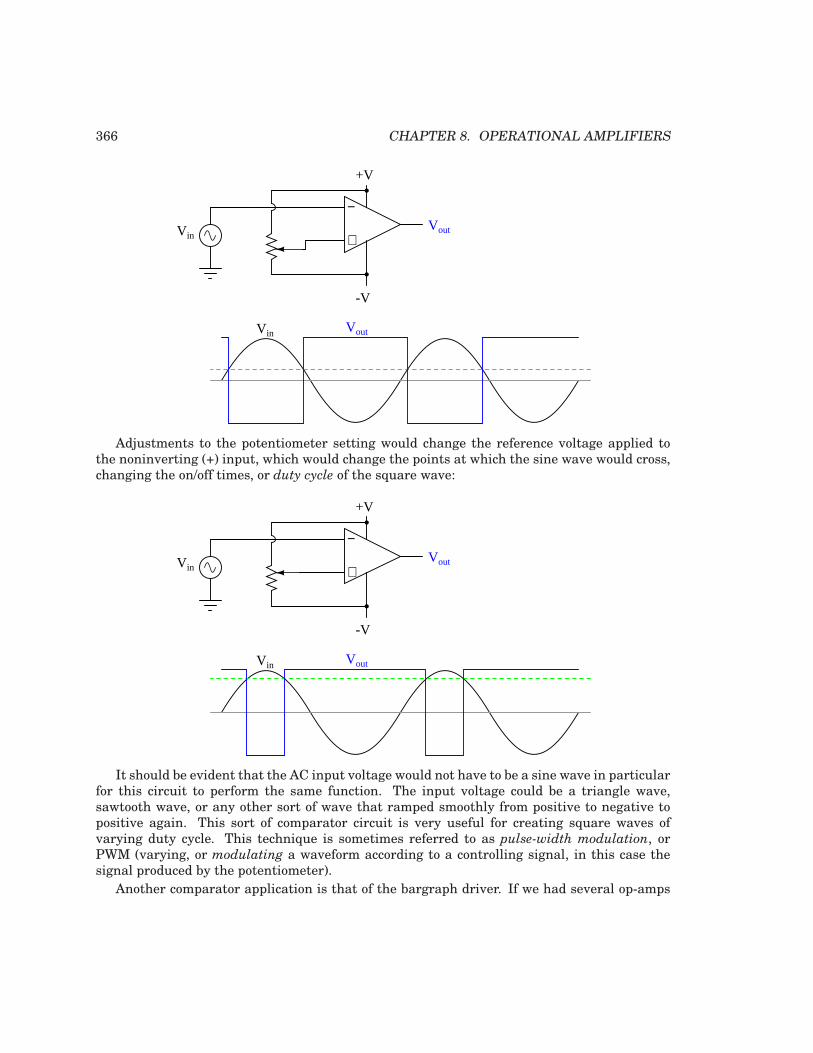
366 CHAPTER 8. OPERATIONAL AMPLIFIERS
−
+
+V
-V
VoutVin
Vin Vout
Adjustments to the potentiometer setting would change the reference voltage applied tothe noninverting (+) input, which would change the points at which the sine wave would cross,changing the on/off times, or duty cycle of the square wave:
−
+
+V
-V
VoutVin
Vin Vout
It should be evident that the AC input voltage would not have to be a sine wave in particularfor this circuit to perform the same function. The input voltage could be a triangle wave,sawtooth wave, or any other sort of wave that ramped smoothly from positive to negative topositive again. This sort of comparator circuit is very useful for creating square waves ofvarying duty cycle. This technique is sometimes referred to as pulse-width modulation, orPWM (varying, or modulating a waveform according to a controlling signal, in this case thesignal produced by the potentiometer).
Another comparator application is that of the bargraph driver. If we had several op-amps
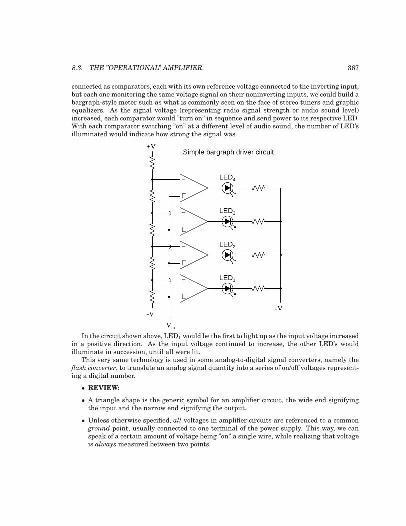
8.3. THE ”OPERATIONAL” AMPLIFIER 367
connected as comparators, each with its own reference voltage connected to the inverting input,but each one monitoring the same voltage signal on their noninverting inputs, we could build abargraph-style meter such as what is commonly seen on the face of stereo tuners and graphicequalizers. As the signal voltage (representing radio signal strength or audio sound level)increased, each comparator would ”turn on” in sequence and send power to its respective LED.With each comparator switching ”on” at a different level of audio sound, the number of LED’silluminated would indicate how strong the signal was.
−
+
−
+
−
+
−
+
+V
-V
Vin
-V
LED1
LED2
LED3
LED4
Simple bargraph driver circuit
In the circuit shown above, LED1 would be the first to light up as the input voltage increasedin a positive direction. As the input voltage continued to increase, the other LED’s wouldilluminate in succession, until all were lit.
This very same technology is used in some analog-to-digital signal converters, namely theflash converter, to translate an analog signal quantity into a series of on/off voltages represent-ing a digital number.
• REVIEW:
• A triangle shape is the generic symbol for an amplifier circuit, the wide end signifyingthe input and the narrow end signifying the output.
• Unless otherwise specified, all voltages in amplifier circuits are referenced to a commonground point, usually connected to one terminal of the power supply. This way, we canspeak of a certain amount of voltage being ”on” a single wire, while realizing that voltageis always measured between two points.
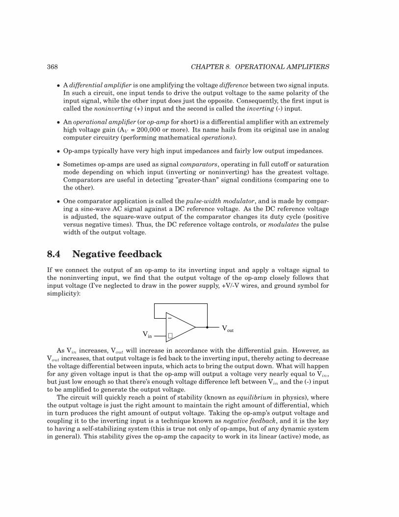
368 CHAPTER 8. OPERATIONAL AMPLIFIERS
• A differential amplifier is one amplifying the voltage difference between two signal inputs.In such a circuit, one input tends to drive the output voltage to the same polarity of theinput signal, while the other input does just the opposite. Consequently, the first input iscalled the noninverting (+) input and the second is called the inverting (-) input.
• An operational amplifier (or op-amp for short) is a differential amplifier with an extremelyhigh voltage gain (AV = 200,000 or more). Its name hails from its original use in analogcomputer circuitry (performing mathematical operations).
• Op-amps typically have very high input impedances and fairly low output impedances.
• Sometimes op-amps are used as signal comparators, operating in full cutoff or saturationmode depending on which input (inverting or noninverting) has the greatest voltage.Comparators are useful in detecting ”greater-than” signal conditions (comparing one tothe other).
• One comparator application is called the pulse-width modulator, and is made by compar-ing a sine-wave AC signal against a DC reference voltage. As the DC reference voltageis adjusted, the square-wave output of the comparator changes its duty cycle (positiveversus negative times). Thus, the DC reference voltage controls, or modulates the pulsewidth of the output voltage.
8.4 Negative feedback
If we connect the output of an op-amp to its inverting input and apply a voltage signal tothe noninverting input, we find that the output voltage of the op-amp closely follows thatinput voltage (I’ve neglected to draw in the power supply, +V/-V wires, and ground symbol forsimplicity):
−
+Vin
Vout
As Vin increases, Vout will increase in accordance with the differential gain. However, asVout increases, that output voltage is fed back to the inverting input, thereby acting to decreasethe voltage differential between inputs, which acts to bring the output down. What will happenfor any given voltage input is that the op-amp will output a voltage very nearly equal to Vin,but just low enough so that there’s enough voltage difference left between Vin and the (-) inputto be amplified to generate the output voltage.
The circuit will quickly reach a point of stability (known as equilibrium in physics), wherethe output voltage is just the right amount to maintain the right amount of differential, whichin turn produces the right amount of output voltage. Taking the op-amp’s output voltage andcoupling it to the inverting input is a technique known as negative feedback, and it is the keyto having a self-stabilizing system (this is true not only of op-amps, but of any dynamic systemin general). This stability gives the op-amp the capacity to work in its linear (active) mode, as
8.4. NEGATIVE FEEDBACK 369
opposed to merely being saturated fully ”on” or ”off” as it was when used as a comparator, withno feedback at all.
Because the op-amp’s gain is so high, the voltage on the inverting input can be maintainedalmost equal to Vin. Let’s say that our op-amp has a differential voltage gain of 200,000. If Vin
equals 6 volts, the output voltage will be 5.999970000149999 volts. This creates just enoughdifferential voltage (6 volts - 5.999970000149999 volts = 29.99985 µV) to cause 5.999970000149999volts to be manifested at the output terminal, and the system holds there in balance. As youcan see, 29.99985 µV is not a lot of differential, so for practical calculations, we can assumethat the differential voltage between the two input wires is held by negative feedback exactlyat 0 volts.
−
+
6 V
5.999970000149999 V
29.99985 µV
The effects of negative feedback
−
+
6 V
The effects of negative feedback
0 V
6 V
(rounded figures)
One great advantage to using an op-amp with negative feedback is that the actual voltagegain of the op-amp doesn’t matter, so long as its very large. If the op-amp’s differential gainwere 250,000 instead of 200,000, all it would mean is that the output voltage would hold justa little closer to Vin (less differential voltage needed between inputs to generate the requiredoutput). In the circuit just illustrated, the output voltage would still be (for all practical pur-poses) equal to the non-inverting input voltage. Op-amp gains, therefore, do not have to beprecisely set by the factory in order for the circuit designer to build an amplifier circuit with
370 CHAPTER 8. OPERATIONAL AMPLIFIERS
precise gain. Negative feedback makes the system self-correcting. The above circuit as a wholewill simply follow the input voltage with a stable gain of 1.
Going back to our differential amplifier model, we can think of the operational amplifieras being a variable voltage source controlled by an extremely sensitive null detector, the kindof meter movement or other sensitive measurement device used in bridge circuits to detect acondition of balance (zero volts). The ”potentiometer” inside the op-amp creating the variablevoltage will move to whatever position it must to ”balance” the inverting and noninvertinginput voltages so that the ”null detector” has zero voltage across it:
null
-
+
+V
-V
6 V
6 V
0 V
As the ”potentiometer” will move to provide an output voltage necessary to satisfy the ”nulldetector” at an ”indication” of zero volts, the output voltage becomes equal to the input voltage:in this case, 6 volts. If the input voltage changes at all, the ”potentiometer” inside the op-ampwill change position to hold the ”null detector” in balance (indicating zero volts), resulting inan output voltage approximately equal to the input voltage at all times.
This will hold true within the range of voltages that the op-amp can output. With a powersupply of +15V/-15V, and an ideal amplifier that can swing its output voltage just as far, itwill faithfully ”follow” the input voltage between the limits of +15 volts and -15 volts. For thisreason, the above circuit is known as a voltage follower. Like its one-transistor counterpart,the common-collector (”emitter-follower”) amplifier, it has a voltage gain of 1, a high inputimpedance, a low output impedance, and a high current gain. Voltage followers are also knownas voltage buffers, and are used to boost the current-sourcing ability of voltage signals too weak(too high of source impedance) to directly drive a load. The op-amp model shown in the lastillustration depicts how the output voltage is essentially isolated from the input voltage, sothat current on the output pin is not supplied by the input voltage source at all, but ratherfrom the power supply powering the op-amp.
It should be mentioned that many op-amps cannot swing their output voltages exactly to+V/-V power supply rail voltages. The model 741 is one of those that cannot: when saturated,its output voltage peaks within about one volt of the +V power supply voltage and within about2 volts of the -V power supply voltage. Therefore, with a split power supply of +15/-15 volts,a 741 op-amp’s output may go as high as +14 volts or as low as -13 volts (approximately), butno further. This is due to its bipolar transistor design. These two voltage limits are known
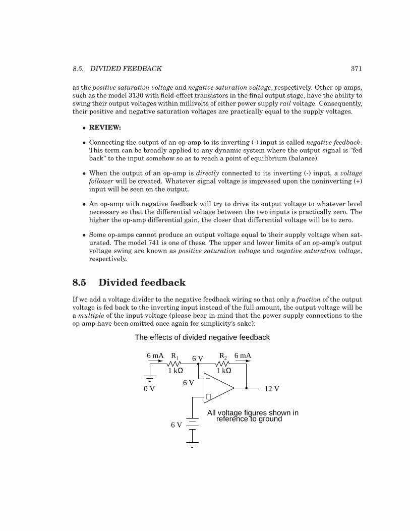
8.5. DIVIDED FEEDBACK 371
as the positive saturation voltage and negative saturation voltage, respectively. Other op-amps,such as the model 3130 with field-effect transistors in the final output stage, have the ability toswing their output voltages within millivolts of either power supply rail voltage. Consequently,their positive and negative saturation voltages are practically equal to the supply voltages.
• REVIEW:
• Connecting the output of an op-amp to its inverting (-) input is called negative feedback.This term can be broadly applied to any dynamic system where the output signal is ”fedback” to the input somehow so as to reach a point of equilibrium (balance).
• When the output of an op-amp is directly connected to its inverting (-) input, a voltage
follower will be created. Whatever signal voltage is impressed upon the noninverting (+)input will be seen on the output.
• An op-amp with negative feedback will try to drive its output voltage to whatever levelnecessary so that the differential voltage between the two inputs is practically zero. Thehigher the op-amp differential gain, the closer that differential voltage will be to zero.
• Some op-amps cannot produce an output voltage equal to their supply voltage when sat-urated. The model 741 is one of these. The upper and lower limits of an op-amp’s outputvoltage swing are known as positive saturation voltage and negative saturation voltage,respectively.
8.5 Divided feedback
If we add a voltage divider to the negative feedback wiring so that only a fraction of the outputvoltage is fed back to the inverting input instead of the full amount, the output voltage will bea multiple of the input voltage (please bear in mind that the power supply connections to theop-amp have been omitted once again for simplicity’s sake):
−
+
6 V
The effects of divided negative feedback
R1 R2
1 kΩ 1 kΩ
0 V
6 V
6 V12 V
All voltage figures shown inreference to ground
6 mA 6 mA
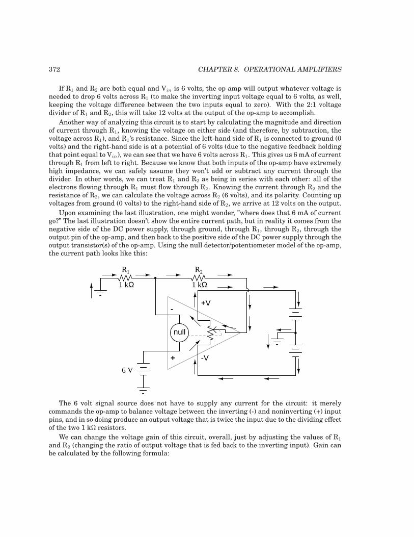
372 CHAPTER 8. OPERATIONAL AMPLIFIERS
If R1 and R2 are both equal and Vin is 6 volts, the op-amp will output whatever voltage isneeded to drop 6 volts across R1 (to make the inverting input voltage equal to 6 volts, as well,keeping the voltage difference between the two inputs equal to zero). With the 2:1 voltagedivider of R1 and R2, this will take 12 volts at the output of the op-amp to accomplish.
Another way of analyzing this circuit is to start by calculating the magnitude and directionof current through R1, knowing the voltage on either side (and therefore, by subtraction, thevoltage across R1), and R1’s resistance. Since the left-hand side of R1 is connected to ground (0volts) and the right-hand side is at a potential of 6 volts (due to the negative feedback holdingthat point equal to Vin), we can see that we have 6 volts across R1. This gives us 6 mA of currentthrough R1 from left to right. Because we know that both inputs of the op-amp have extremelyhigh impedance, we can safely assume they won’t add or subtract any current through thedivider. In other words, we can treat R1 and R2 as being in series with each other: all of theelectrons flowing through R1 must flow through R2. Knowing the current through R2 and theresistance of R2, we can calculate the voltage across R2 (6 volts), and its polarity. Counting upvoltages from ground (0 volts) to the right-hand side of R2, we arrive at 12 volts on the output.
Upon examining the last illustration, one might wonder, ”where does that 6 mA of currentgo?” The last illustration doesn’t show the entire current path, but in reality it comes from thenegative side of the DC power supply, through ground, through R1, through R2, through theoutput pin of the op-amp, and then back to the positive side of the DC power supply through theoutput transistor(s) of the op-amp. Using the null detector/potentiometer model of the op-amp,the current path looks like this:
null
-
+
+V
-V
6 V
R1 R2
1 kΩ 1 kΩ
The 6 volt signal source does not have to supply any current for the circuit: it merelycommands the op-amp to balance voltage between the inverting (-) and noninverting (+) inputpins, and in so doing produce an output voltage that is twice the input due to the dividing effectof the two 1 kΩ resistors.
We can change the voltage gain of this circuit, overall, just by adjusting the values of R1
and R2 (changing the ratio of output voltage that is fed back to the inverting input). Gain canbe calculated by the following formula:
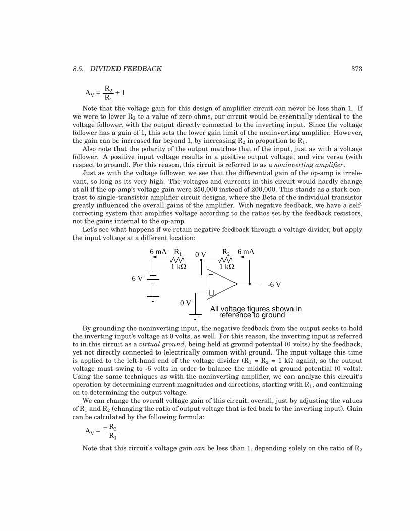
8.5. DIVIDED FEEDBACK 373
AV = R2
R1+ 1
Note that the voltage gain for this design of amplifier circuit can never be less than 1. Ifwe were to lower R2 to a value of zero ohms, our circuit would be essentially identical to thevoltage follower, with the output directly connected to the inverting input. Since the voltagefollower has a gain of 1, this sets the lower gain limit of the noninverting amplifier. However,the gain can be increased far beyond 1, by increasing R2 in proportion to R1.
Also note that the polarity of the output matches that of the input, just as with a voltagefollower. A positive input voltage results in a positive output voltage, and vice versa (withrespect to ground). For this reason, this circuit is referred to as a noninverting amplifier.
Just as with the voltage follower, we see that the differential gain of the op-amp is irrele-vant, so long as its very high. The voltages and currents in this circuit would hardly changeat all if the op-amp’s voltage gain were 250,000 instead of 200,000. This stands as a stark con-trast to single-transistor amplifier circuit designs, where the Beta of the individual transistorgreatly influenced the overall gains of the amplifier. With negative feedback, we have a self-correcting system that amplifies voltage according to the ratios set by the feedback resistors,not the gains internal to the op-amp.
Let’s see what happens if we retain negative feedback through a voltage divider, but applythe input voltage at a different location:
−
+
6 V
R1 R2
1 kΩ 1 kΩ
0 VAll voltage figures shown in
reference to ground
0 V
-6 V
6 mA 6 mA
By grounding the noninverting input, the negative feedback from the output seeks to holdthe inverting input’s voltage at 0 volts, as well. For this reason, the inverting input is referredto in this circuit as a virtual ground, being held at ground potential (0 volts) by the feedback,yet not directly connected to (electrically common with) ground. The input voltage this timeis applied to the left-hand end of the voltage divider (R1 = R2 = 1 kΩ again), so the outputvoltage must swing to -6 volts in order to balance the middle at ground potential (0 volts).Using the same techniques as with the noninverting amplifier, we can analyze this circuit’soperation by determining current magnitudes and directions, starting with R1, and continuingon to determining the output voltage.
We can change the overall voltage gain of this circuit, overall, just by adjusting the valuesof R1 and R2 (changing the ratio of output voltage that is fed back to the inverting input). Gaincan be calculated by the following formula:
AV = R2
R1
−
Note that this circuit’s voltage gain can be less than 1, depending solely on the ratio of R2
374 CHAPTER 8. OPERATIONAL AMPLIFIERS
to R1. Also note that the output voltage is always the opposite polarity of the input voltage.A positive input voltage results in a negative output voltage, and vice versa (with respect toground). For this reason, this circuit is referred to as an inverting amplifier. Sometimes, thegain formula contains a negative sign (before the R2/R1 fraction) to reflect this reversal ofpolarities.
These two amplifier circuits we’ve just investigated serve the purpose of multiplying ordividing the magnitude of the input voltage signal. This is exactly how the mathematicaloperations of multiplication and division are typically handled in analog computer circuitry.
• REVIEW:
• By connecting the inverting (-) input of an op-amp directly to the output, we get negativefeedback, which gives us a voltage follower circuit. By connecting that negative feedbackthrough a resistive voltage divider (feeding back a fraction of the output voltage to theinverting input), the output voltage becomes a multiple of the input voltage.
• A negative-feedback op-amp circuit with the input signal going to the noninverting (+)input is called a noninverting amplifier. The output voltage will be the same polarity asthe input. Voltage gain is given by the following equation: AV = (R2/R1) + 1
• A negative-feedback op-amp circuit with the input signal going to the ”bottom” of theresistive voltage divider, with the noninverting (+) input grounded, is called an inverting
amplifier. Its output voltage will be the opposite polarity of the input. Voltage gain isgiven by the following equation: AV = -R2/R1
8.6 An analogy for divided feedback
A helpful analogy for understanding divided feedback amplifier circuits is that of a mechanicallever, with relative motion of the lever’s ends representing change in input and output voltages,and the fulcrum (pivot point) representing the location of the ground point, real or virtual.
Take for example the following noninverting op-amp circuit. We know from the prior sectionthat the voltage gain of a noninverting amplifier configuration can never be less than unity (1).If we draw a lever diagram next to the amplifier schematic, with the distance between fulcrumand lever ends representative of resistor values, the motion of the lever will signify changes involtage at the input and output terminals of the amplifier:
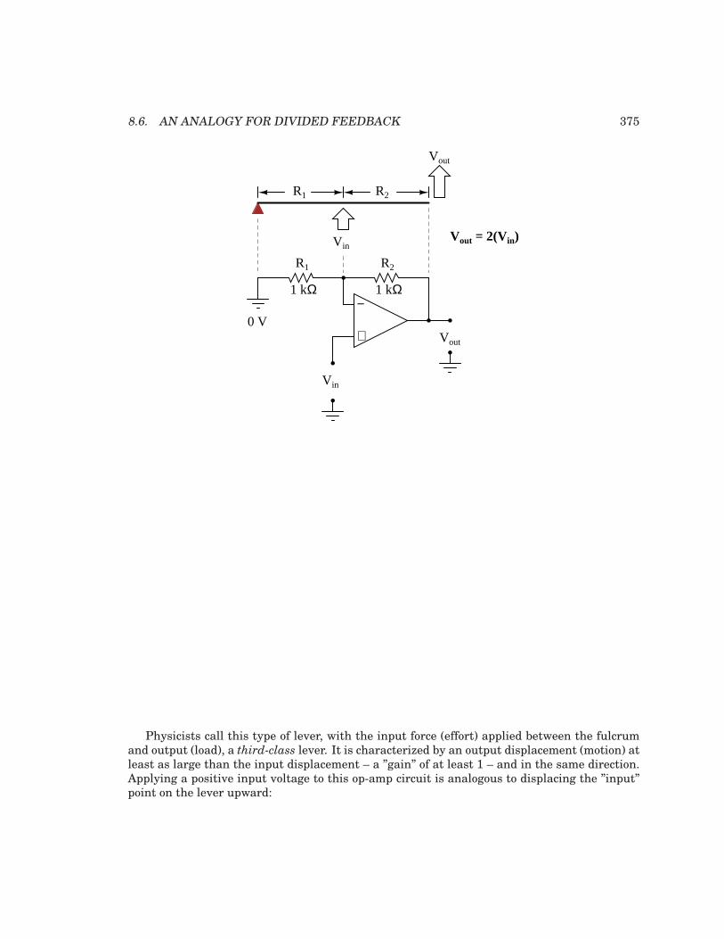
8.6. AN ANALOGY FOR DIVIDED FEEDBACK 375
−
+
R1 R2
1 kΩ 1 kΩ
0 V
Vin
Vin
Vout
R1 R2
Vout = 2(Vin)
Vout
Physicists call this type of lever, with the input force (effort) applied between the fulcrumand output (load), a third-class lever. It is characterized by an output displacement (motion) atleast as large than the input displacement – a ”gain” of at least 1 – and in the same direction.Applying a positive input voltage to this op-amp circuit is analogous to displacing the ”input”point on the lever upward:
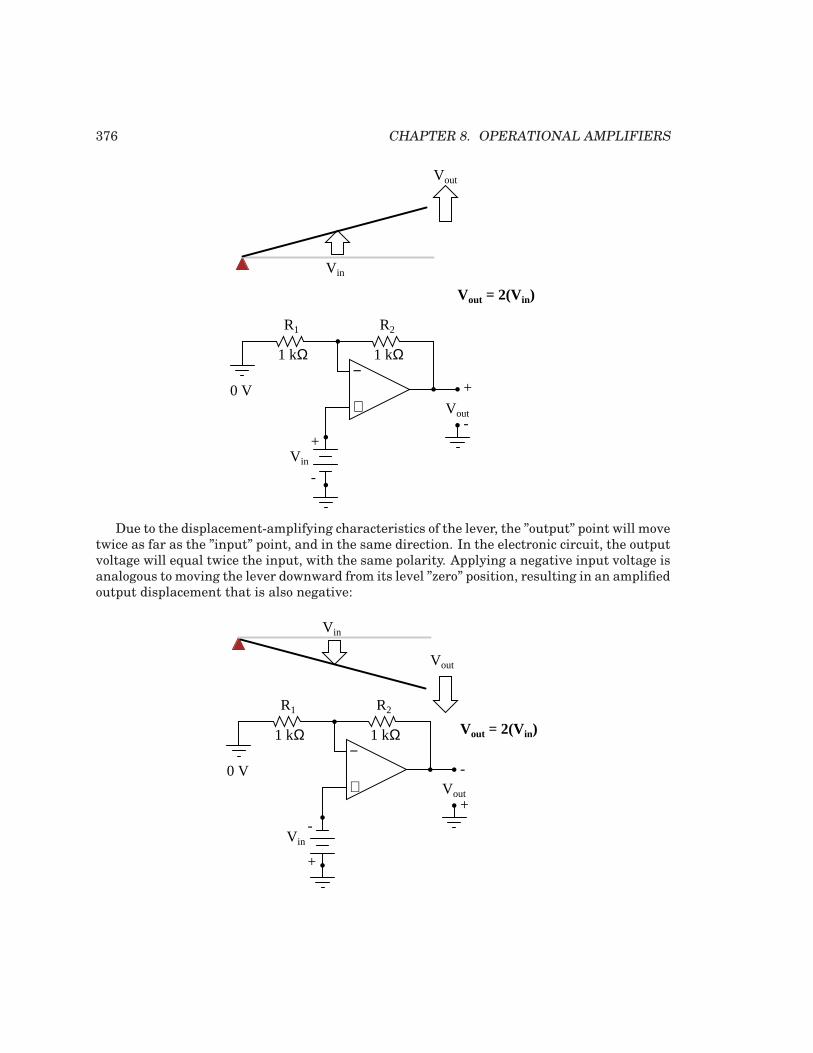
376 CHAPTER 8. OPERATIONAL AMPLIFIERS
−
+
R1 R2
1 kΩ 1 kΩ
0 V
Vin
Vin
Vout
Vout = 2(Vin)
Vout
+
-
+
-
Due to the displacement-amplifying characteristics of the lever, the ”output” point will movetwice as far as the ”input” point, and in the same direction. In the electronic circuit, the outputvoltage will equal twice the input, with the same polarity. Applying a negative input voltage isanalogous to moving the lever downward from its level ”zero” position, resulting in an amplifiedoutput displacement that is also negative:
−
+
R1 R2
1 kΩ 1 kΩ
0 V
Vin
Vin
Vout
Vout = 2(Vin)
Vout
+
-
+
-
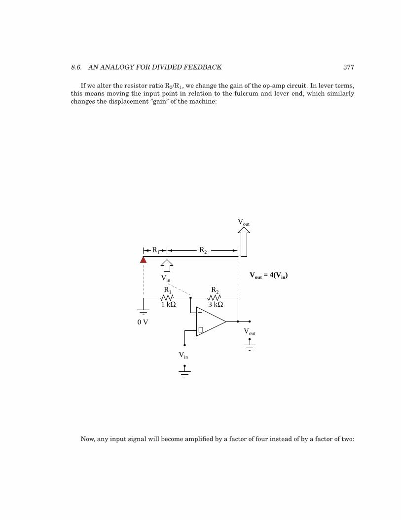
8.6. AN ANALOGY FOR DIVIDED FEEDBACK 377
If we alter the resistor ratio R2/R1, we change the gain of the op-amp circuit. In lever terms,this means moving the input point in relation to the fulcrum and lever end, which similarlychanges the displacement ”gain” of the machine:
−
+
R1 R2
1 kΩ
0 V
Vin
Vin
Vout
R1 R2
Vout
3 kΩ
Vout = 4(Vin)
Now, any input signal will become amplified by a factor of four instead of by a factor of two:
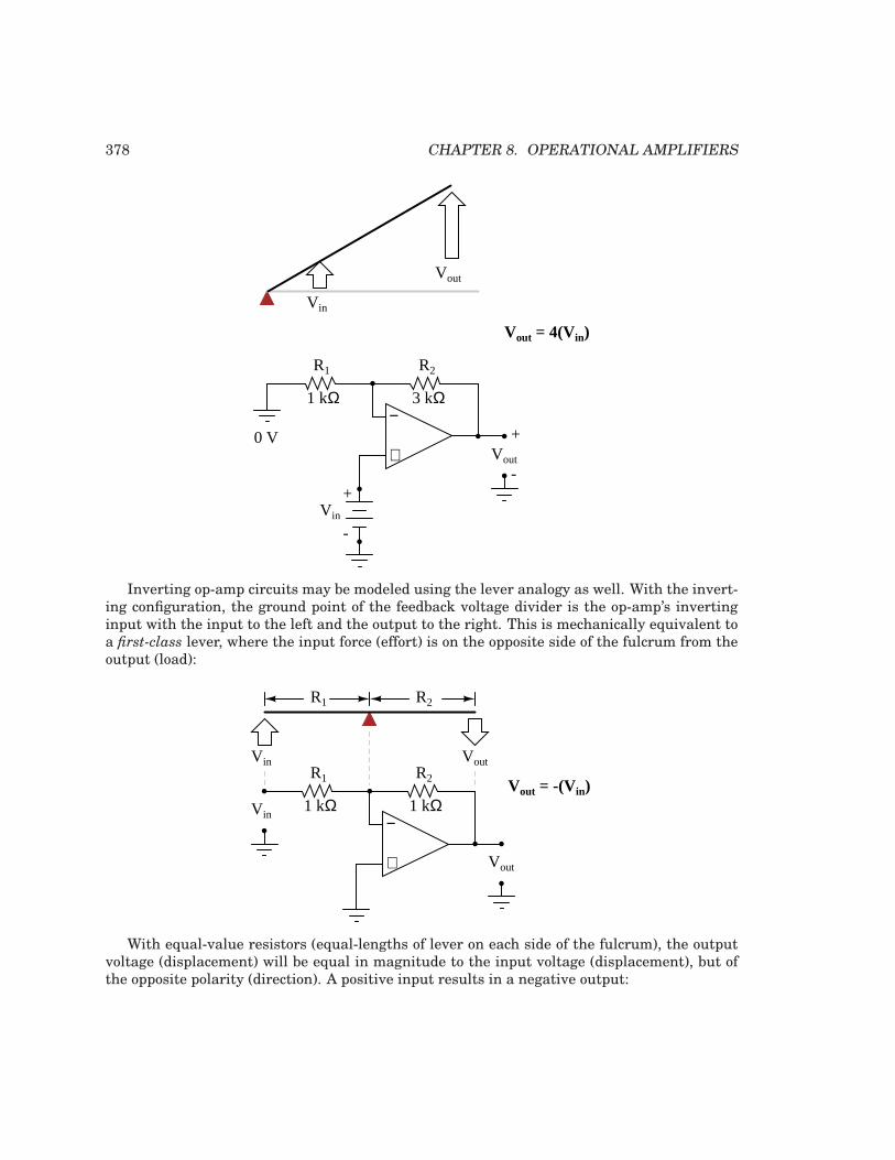
378 CHAPTER 8. OPERATIONAL AMPLIFIERS
−
+
R1 R2
1 kΩ
0 V
Vin
Vin
Vout
Vout
3 kΩ
Vout = 4(Vin)
+
-
+
-
Inverting op-amp circuits may be modeled using the lever analogy as well. With the invert-ing configuration, the ground point of the feedback voltage divider is the op-amp’s invertinginput with the input to the left and the output to the right. This is mechanically equivalent toa first-class lever, where the input force (effort) is on the opposite side of the fulcrum from theoutput (load):
−
+
R1 R2
1 kΩ 1 kΩVin
Vout
Vin Vout
Vout = -(Vin)
R1 R2
With equal-value resistors (equal-lengths of lever on each side of the fulcrum), the outputvoltage (displacement) will be equal in magnitude to the input voltage (displacement), but ofthe opposite polarity (direction). A positive input results in a negative output:
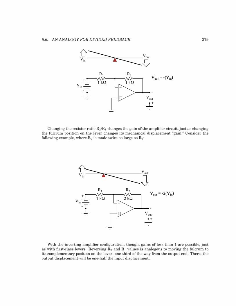
8.6. AN ANALOGY FOR DIVIDED FEEDBACK 379
−
+
R1 R2
1 kΩ 1 kΩVin
Vout
Vin
Vout
Vout = -(Vin)
+
--
+
Changing the resistor ratio R2/R1 changes the gain of the amplifier circuit, just as changingthe fulcrum position on the lever changes its mechanical displacement ”gain.” Consider thefollowing example, where R2 is made twice as large as R1:
−
+
R1 R2
1 kΩVin
Vout
Vin
Vout
+
--
+2 kΩ
Vout = -2(Vin)
With the inverting amplifier configuration, though, gains of less than 1 are possible, justas with first-class levers. Reversing R2 and R1 values is analogous to moving the fulcrum toits complementary position on the lever: one-third of the way from the output end. There, theoutput displacement will be one-half the input displacement:
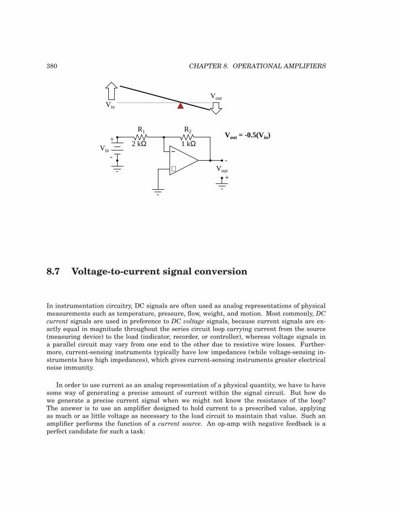
380 CHAPTER 8. OPERATIONAL AMPLIFIERS
−
+
R1 R2
1 kΩVin
Vout
Vin
Vout
+
--
+2 kΩ
Vout = -0.5(Vin)
8.7 Voltage-to-current signal conversion
In instrumentation circuitry, DC signals are often used as analog representations of physicalmeasurements such as temperature, pressure, flow, weight, and motion. Most commonly, DC
current signals are used in preference to DC voltage signals, because current signals are ex-actly equal in magnitude throughout the series circuit loop carrying current from the source(measuring device) to the load (indicator, recorder, or controller), whereas voltage signals ina parallel circuit may vary from one end to the other due to resistive wire losses. Further-more, current-sensing instruments typically have low impedances (while voltage-sensing in-struments have high impedances), which gives current-sensing instruments greater electricalnoise immunity.
In order to use current as an analog representation of a physical quantity, we have to havesome way of generating a precise amount of current within the signal circuit. But how dowe generate a precise current signal when we might not know the resistance of the loop?The answer is to use an amplifier designed to hold current to a prescribed value, applyingas much or as little voltage as necessary to the load circuit to maintain that value. Such anamplifier performs the function of a current source. An op-amp with negative feedback is aperfect candidate for such a task:
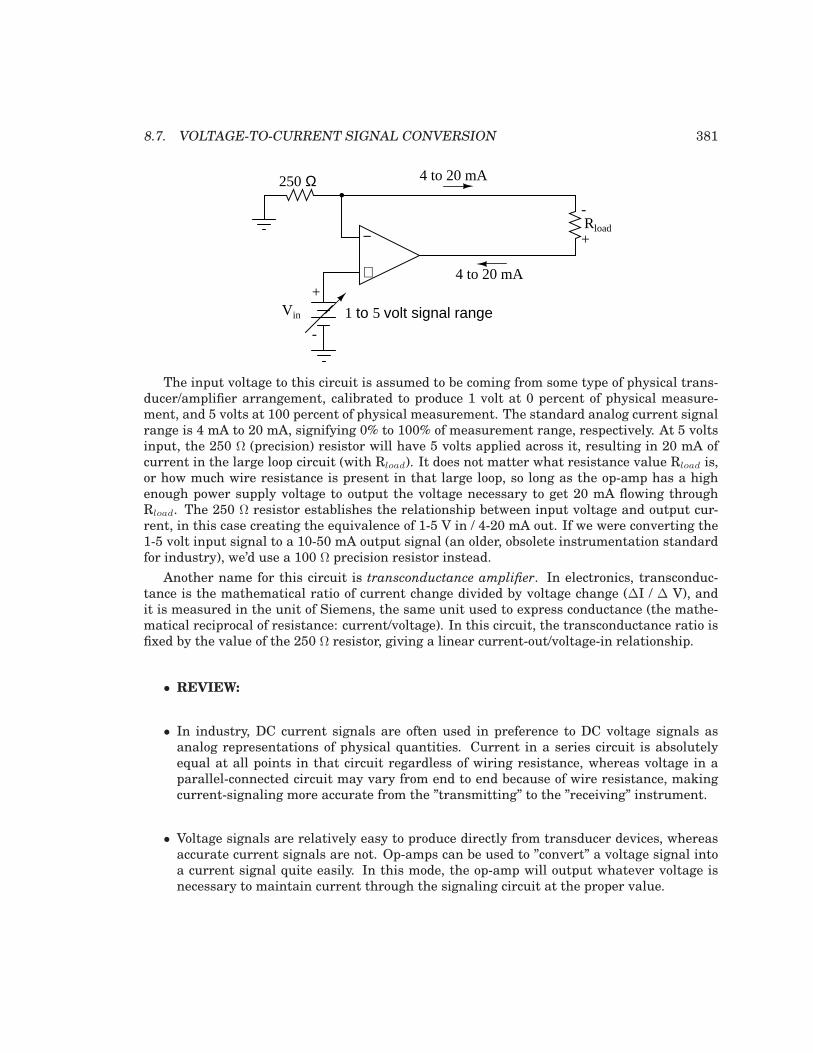
8.7. VOLTAGE-TO-CURRENT SIGNAL CONVERSION 381
−
+
Vin 1 to 5 volt signal range
Rload
250 Ω 4 to 20 mA
4 to 20 mA
+
-
+
-
The input voltage to this circuit is assumed to be coming from some type of physical trans-ducer/amplifier arrangement, calibrated to produce 1 volt at 0 percent of physical measure-ment, and 5 volts at 100 percent of physical measurement. The standard analog current signalrange is 4 mA to 20 mA, signifying 0% to 100% of measurement range, respectively. At 5 voltsinput, the 250 Ω (precision) resistor will have 5 volts applied across it, resulting in 20 mA ofcurrent in the large loop circuit (with Rload). It does not matter what resistance value Rload is,or how much wire resistance is present in that large loop, so long as the op-amp has a highenough power supply voltage to output the voltage necessary to get 20 mA flowing throughRload. The 250 Ω resistor establishes the relationship between input voltage and output cur-rent, in this case creating the equivalence of 1-5 V in / 4-20 mA out. If we were converting the1-5 volt input signal to a 10-50 mA output signal (an older, obsolete instrumentation standardfor industry), we’d use a 100 Ω precision resistor instead.
Another name for this circuit is transconductance amplifier. In electronics, transconduc-tance is the mathematical ratio of current change divided by voltage change (∆I / ∆ V), andit is measured in the unit of Siemens, the same unit used to express conductance (the mathe-matical reciprocal of resistance: current/voltage). In this circuit, the transconductance ratio isfixed by the value of the 250 Ω resistor, giving a linear current-out/voltage-in relationship.
• REVIEW:
• In industry, DC current signals are often used in preference to DC voltage signals asanalog representations of physical quantities. Current in a series circuit is absolutelyequal at all points in that circuit regardless of wiring resistance, whereas voltage in aparallel-connected circuit may vary from end to end because of wire resistance, makingcurrent-signaling more accurate from the ”transmitting” to the ”receiving” instrument.
• Voltage signals are relatively easy to produce directly from transducer devices, whereasaccurate current signals are not. Op-amps can be used to ”convert” a voltage signal intoa current signal quite easily. In this mode, the op-amp will output whatever voltage isnecessary to maintain current through the signaling circuit at the proper value.
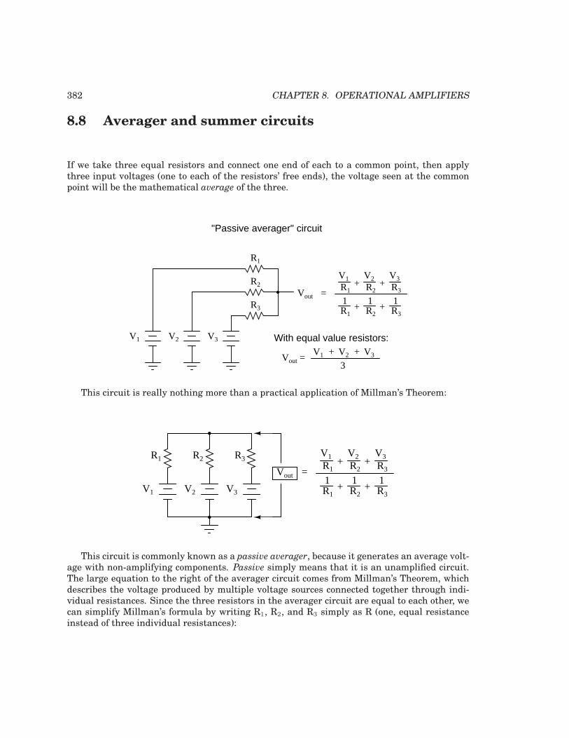
382 CHAPTER 8. OPERATIONAL AMPLIFIERS
8.8 Averager and summer circuits
If we take three equal resistors and connect one end of each to a common point, then applythree input voltages (one to each of the resistors’ free ends), the voltage seen at the commonpoint will be the mathematical average of the three.
R1
R2
R3
V1 V2 V3
Vout
V1 V2 V3
=+ +R1 R2 R3
R1+ R2
+ R3
1 1 1
"Passive averager" circuit
With equal value resistors:
Vout = V1 V2 V3+ +
3
This circuit is really nothing more than a practical application of Millman’s Theorem:
R1 R2 R3
V1 V2 V3
Vout
V1 V2 V3
=+ +R1 R2 R3
R1+ R2
+ R3
1 1 1
This circuit is commonly known as a passive averager, because it generates an average volt-age with non-amplifying components. Passive simply means that it is an unamplified circuit.The large equation to the right of the averager circuit comes from Millman’s Theorem, whichdescribes the voltage produced by multiple voltage sources connected together through indi-vidual resistances. Since the three resistors in the averager circuit are equal to each other, wecan simplify Millman’s formula by writing R1, R2, and R3 simply as R (one, equal resistanceinstead of three individual resistances):
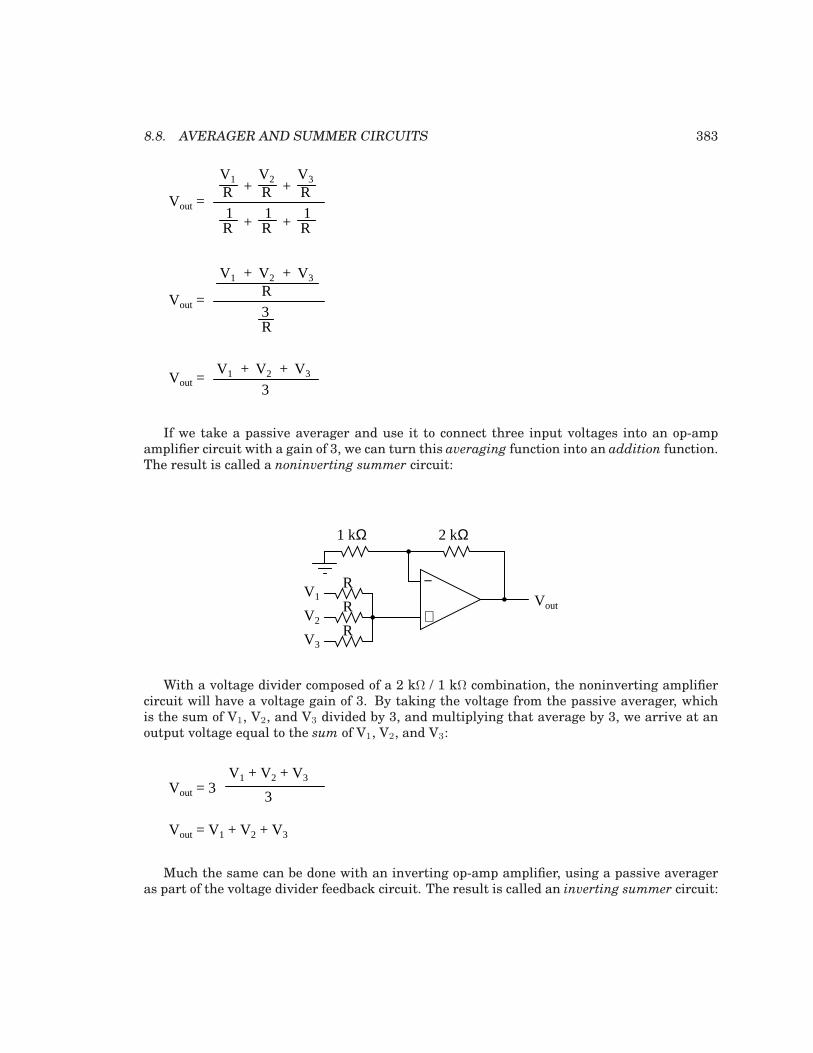
8.8. AVERAGER AND SUMMER CIRCUITS 383
V1 V2 V3+ +
+ +1 1 1
Vout = V1 V2 V3+ +
3
Vout = R R R
R R R
Vout =
V1 V2 V3+ +R
3R
If we take a passive averager and use it to connect three input voltages into an op-ampamplifier circuit with a gain of 3, we can turn this averaging function into an addition function.The result is called a noninverting summer circuit:
−
+
1 kΩ 2 kΩ
R
R
R
V1
V2
V3
Vout
With a voltage divider composed of a 2 kΩ / 1 kΩ combination, the noninverting amplifiercircuit will have a voltage gain of 3. By taking the voltage from the passive averager, whichis the sum of V1, V2, and V3 divided by 3, and multiplying that average by 3, we arrive at anoutput voltage equal to the sum of V1, V2, and V3:
Vout = 3V1 + V2 + V3
3
Vout = V1 + V2 + V3
Much the same can be done with an inverting op-amp amplifier, using a passive averageras part of the voltage divider feedback circuit. The result is called an inverting summer circuit:
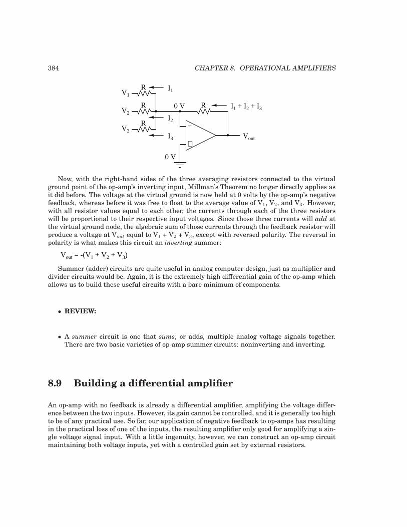
384 CHAPTER 8. OPERATIONAL AMPLIFIERS
−
+
R
R
R
V1
V2
V3Vout
R
I1
I3
I2
I1 + I2 + I30 V
0 V
Now, with the right-hand sides of the three averaging resistors connected to the virtualground point of the op-amp’s inverting input, Millman’s Theorem no longer directly applies asit did before. The voltage at the virtual ground is now held at 0 volts by the op-amp’s negativefeedback, whereas before it was free to float to the average value of V1, V2, and V3. However,with all resistor values equal to each other, the currents through each of the three resistorswill be proportional to their respective input voltages. Since those three currents will add atthe virtual ground node, the algebraic sum of those currents through the feedback resistor willproduce a voltage at Vout equal to V1 + V2 + V3, except with reversed polarity. The reversal inpolarity is what makes this circuit an inverting summer:
Vout = -(V1 + V2 + V3)
Summer (adder) circuits are quite useful in analog computer design, just as multiplier anddivider circuits would be. Again, it is the extremely high differential gain of the op-amp whichallows us to build these useful circuits with a bare minimum of components.
• REVIEW:
• A summer circuit is one that sums, or adds, multiple analog voltage signals together.There are two basic varieties of op-amp summer circuits: noninverting and inverting.
8.9 Building a differential amplifier
An op-amp with no feedback is already a differential amplifier, amplifying the voltage differ-ence between the two inputs. However, its gain cannot be controlled, and it is generally too highto be of any practical use. So far, our application of negative feedback to op-amps has resultingin the practical loss of one of the inputs, the resulting amplifier only good for amplifying a sin-gle voltage signal input. With a little ingenuity, however, we can construct an op-amp circuitmaintaining both voltage inputs, yet with a controlled gain set by external resistors.
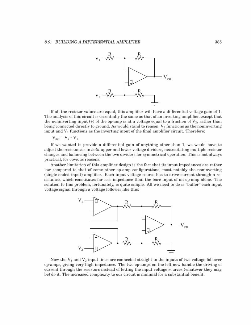
8.9. BUILDING A DIFFERENTIAL AMPLIFIER 385
−
+
V1
V2
Vout
R R
R R
If all the resistor values are equal, this amplifier will have a differential voltage gain of 1.The analysis of this circuit is essentially the same as that of an inverting amplifier, except thatthe noninverting input (+) of the op-amp is at a voltage equal to a fraction of V2, rather thanbeing connected directly to ground. As would stand to reason, V2 functions as the noninvertinginput and V1 functions as the inverting input of the final amplifier circuit. Therefore:
Vout = V2 - V1
If we wanted to provide a differential gain of anything other than 1, we would have toadjust the resistances in both upper and lower voltage dividers, necessitating multiple resistorchanges and balancing between the two dividers for symmetrical operation. This is not alwayspractical, for obvious reasons.
Another limitation of this amplifier design is the fact that its input impedances are ratherlow compared to that of some other op-amp configurations, most notably the noninverting(single-ended input) amplifier. Each input voltage source has to drive current through a re-sistance, which constitutes far less impedance than the bare input of an op-amp alone. Thesolution to this problem, fortunately, is quite simple. All we need to do is ”buffer” each inputvoltage signal through a voltage follower like this:
−
+
V1
V2
Vout
R R
R R
−
+
−
+
Now the V1 and V2 input lines are connected straight to the inputs of two voltage-followerop-amps, giving very high impedance. The two op-amps on the left now handle the driving ofcurrent through the resistors instead of letting the input voltage sources (whatever they maybe) do it. The increased complexity to our circuit is minimal for a substantial benefit.
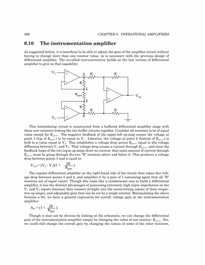
386 CHAPTER 8. OPERATIONAL AMPLIFIERS
8.10 The instrumentation amplifier
As suggested before, it is beneficial to be able to adjust the gain of the amplifier circuit withouthaving to change more than one resistor value, as is necessary with the previous design ofdifferential amplifier. The so-called instrumentation builds on the last version of differentialamplifier to give us that capability:
−
+
V1
V2
Vout
R R
R R
−
+
−
+
R
R
Rgain
3
1
2
4
This intimidating circuit is constructed from a buffered differential amplifier stage withthree new resistors linking the two buffer circuits together. Consider all resistors to be of equalvalue except for Rgain. The negative feedback of the upper-left op-amp causes the voltage atpoint 1 (top of Rgain) to be equal to V1. Likewise, the voltage at point 2 (bottom of Rgain) isheld to a value equal to V2. This establishes a voltage drop across Rgain equal to the voltagedifference between V1 and V2. That voltage drop causes a current through Rgain, and since thefeedback loops of the two input op-amps draw no current, that same amount of current throughRgain must be going through the two ”R” resistors above and below it. This produces a voltagedrop between points 3 and 4 equal to:
V3-4 = (V2 - V1)(1 + 2RRgain
)
The regular differential amplifier on the right-hand side of the circuit then takes this volt-age drop between points 3 and 4, and amplifies it by a gain of 1 (assuming again that all ”R”resistors are of equal value). Though this looks like a cumbersome way to build a differentialamplifier, it has the distinct advantages of possessing extremely high input impedances on theV1 and V2 inputs (because they connect straight into the noninverting inputs of their respec-tive op-amps), and adjustable gain that can be set by a single resistor. Manipulating the aboveformula a bit, we have a general expression for overall voltage gain in the instrumentationamplifier:
2RRgain
)AV = (1 +
Though it may not be obvious by looking at the schematic, we can change the differentialgain of the instrumentation amplifier simply by changing the value of one resistor: Rgain. Yes,we could still change the overall gain by changing the values of some of the other resistors,
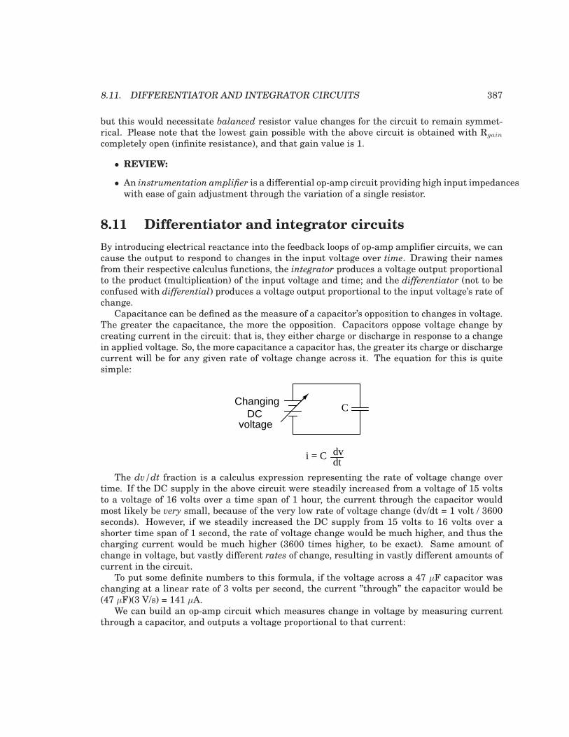
8.11. DIFFERENTIATOR AND INTEGRATOR CIRCUITS 387
but this would necessitate balanced resistor value changes for the circuit to remain symmet-rical. Please note that the lowest gain possible with the above circuit is obtained with Rgain
completely open (infinite resistance), and that gain value is 1.
• REVIEW:
• An instrumentation amplifier is a differential op-amp circuit providing high input impedanceswith ease of gain adjustment through the variation of a single resistor.
8.11 Differentiator and integrator circuits
By introducing electrical reactance into the feedback loops of op-amp amplifier circuits, we cancause the output to respond to changes in the input voltage over time. Drawing their namesfrom their respective calculus functions, the integrator produces a voltage output proportionalto the product (multiplication) of the input voltage and time; and the differentiator (not to beconfused with differential) produces a voltage output proportional to the input voltage’s rate ofchange.
Capacitance can be defined as the measure of a capacitor’s opposition to changes in voltage.The greater the capacitance, the more the opposition. Capacitors oppose voltage change bycreating current in the circuit: that is, they either charge or discharge in response to a changein applied voltage. So, the more capacitance a capacitor has, the greater its charge or dischargecurrent will be for any given rate of voltage change across it. The equation for this is quitesimple:
ChangingDC
voltage
C
i = C dvdt
The dv/dt fraction is a calculus expression representing the rate of voltage change overtime. If the DC supply in the above circuit were steadily increased from a voltage of 15 voltsto a voltage of 16 volts over a time span of 1 hour, the current through the capacitor wouldmost likely be very small, because of the very low rate of voltage change (dv/dt = 1 volt / 3600seconds). However, if we steadily increased the DC supply from 15 volts to 16 volts over ashorter time span of 1 second, the rate of voltage change would be much higher, and thus thecharging current would be much higher (3600 times higher, to be exact). Same amount ofchange in voltage, but vastly different rates of change, resulting in vastly different amounts ofcurrent in the circuit.
To put some definite numbers to this formula, if the voltage across a 47 µF capacitor waschanging at a linear rate of 3 volts per second, the current ”through” the capacitor would be(47 µF)(3 V/s) = 141 µA.
We can build an op-amp circuit which measures change in voltage by measuring currentthrough a capacitor, and outputs a voltage proportional to that current:
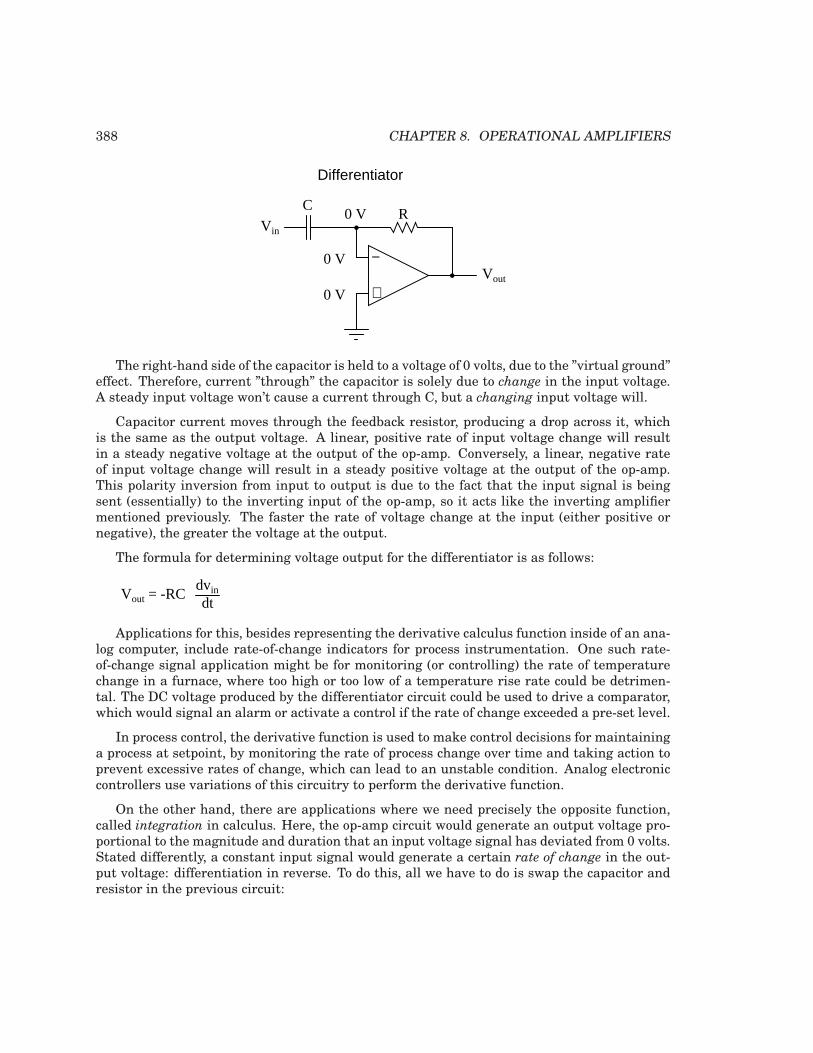
388 CHAPTER 8. OPERATIONAL AMPLIFIERS
−
+
Vin
Vout
CR
0 V
0 V
0 V
Differentiator
The right-hand side of the capacitor is held to a voltage of 0 volts, due to the ”virtual ground”effect. Therefore, current ”through” the capacitor is solely due to change in the input voltage.A steady input voltage won’t cause a current through C, but a changing input voltage will.
Capacitor current moves through the feedback resistor, producing a drop across it, whichis the same as the output voltage. A linear, positive rate of input voltage change will resultin a steady negative voltage at the output of the op-amp. Conversely, a linear, negative rateof input voltage change will result in a steady positive voltage at the output of the op-amp.This polarity inversion from input to output is due to the fact that the input signal is beingsent (essentially) to the inverting input of the op-amp, so it acts like the inverting amplifiermentioned previously. The faster the rate of voltage change at the input (either positive ornegative), the greater the voltage at the output.
The formula for determining voltage output for the differentiator is as follows:
Vout = -RCdvin
dt
Applications for this, besides representing the derivative calculus function inside of an ana-log computer, include rate-of-change indicators for process instrumentation. One such rate-of-change signal application might be for monitoring (or controlling) the rate of temperaturechange in a furnace, where too high or too low of a temperature rise rate could be detrimen-tal. The DC voltage produced by the differentiator circuit could be used to drive a comparator,which would signal an alarm or activate a control if the rate of change exceeded a pre-set level.
In process control, the derivative function is used to make control decisions for maintaininga process at setpoint, by monitoring the rate of process change over time and taking action toprevent excessive rates of change, which can lead to an unstable condition. Analog electroniccontrollers use variations of this circuitry to perform the derivative function.
On the other hand, there are applications where we need precisely the opposite function,called integration in calculus. Here, the op-amp circuit would generate an output voltage pro-portional to the magnitude and duration that an input voltage signal has deviated from 0 volts.Stated differently, a constant input signal would generate a certain rate of change in the out-put voltage: differentiation in reverse. To do this, all we have to do is swap the capacitor andresistor in the previous circuit:
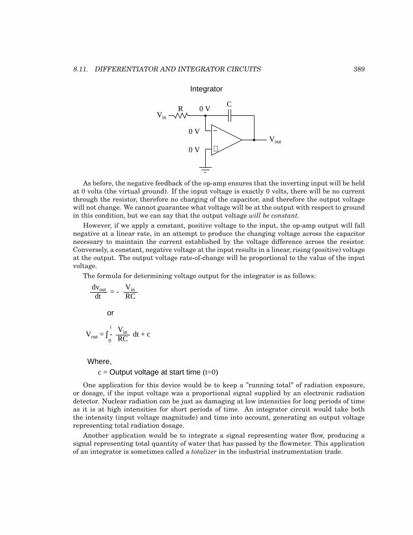
8.11. DIFFERENTIATOR AND INTEGRATOR CIRCUITS 389
−
+
Vin
Vout
CR
0 V
0 V
0 V
Integrator
As before, the negative feedback of the op-amp ensures that the inverting input will be heldat 0 volts (the virtual ground). If the input voltage is exactly 0 volts, there will be no currentthrough the resistor, therefore no charging of the capacitor, and therefore the output voltagewill not change. We cannot guarantee what voltage will be at the output with respect to groundin this condition, but we can say that the output voltage will be constant.
However, if we apply a constant, positive voltage to the input, the op-amp output will fallnegative at a linear rate, in an attempt to produce the changing voltage across the capacitornecessary to maintain the current established by the voltage difference across the resistor.Conversely, a constant, negative voltage at the input results in a linear, rising (positive) voltageat the output. The output voltage rate-of-change will be proportional to the value of the inputvoltage.
The formula for determining voltage output for the integrator is as follows:
dvout
dt= -
Vin
RC
or
Vin
RCdt + c
t
0
Where,c = Output voltage at start time (t=0)
Vout = ∫ -
One application for this device would be to keep a ”running total” of radiation exposure,or dosage, if the input voltage was a proportional signal supplied by an electronic radiationdetector. Nuclear radiation can be just as damaging at low intensities for long periods of timeas it is at high intensities for short periods of time. An integrator circuit would take boththe intensity (input voltage magnitude) and time into account, generating an output voltagerepresenting total radiation dosage.
Another application would be to integrate a signal representing water flow, producing asignal representing total quantity of water that has passed by the flowmeter. This applicationof an integrator is sometimes called a totalizer in the industrial instrumentation trade.
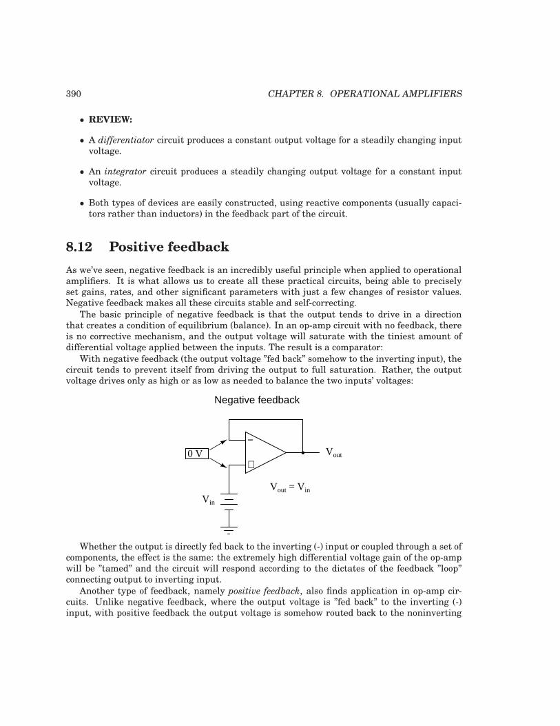
390 CHAPTER 8. OPERATIONAL AMPLIFIERS
• REVIEW:
• A differentiator circuit produces a constant output voltage for a steadily changing inputvoltage.
• An integrator circuit produces a steadily changing output voltage for a constant inputvoltage.
• Both types of devices are easily constructed, using reactive components (usually capaci-tors rather than inductors) in the feedback part of the circuit.
8.12 Positive feedback
As we’ve seen, negative feedback is an incredibly useful principle when applied to operationalamplifiers. It is what allows us to create all these practical circuits, being able to preciselyset gains, rates, and other significant parameters with just a few changes of resistor values.Negative feedback makes all these circuits stable and self-correcting.
The basic principle of negative feedback is that the output tends to drive in a directionthat creates a condition of equilibrium (balance). In an op-amp circuit with no feedback, thereis no corrective mechanism, and the output voltage will saturate with the tiniest amount ofdifferential voltage applied between the inputs. The result is a comparator:
With negative feedback (the output voltage ”fed back” somehow to the inverting input), thecircuit tends to prevent itself from driving the output to full saturation. Rather, the outputvoltage drives only as high or as low as needed to balance the two inputs’ voltages:
−
+0 V
Vin
Vout
Vout = Vin
Negative feedback
Whether the output is directly fed back to the inverting (-) input or coupled through a set ofcomponents, the effect is the same: the extremely high differential voltage gain of the op-ampwill be ”tamed” and the circuit will respond according to the dictates of the feedback ”loop”connecting output to inverting input.
Another type of feedback, namely positive feedback, also finds application in op-amp cir-cuits. Unlike negative feedback, where the output voltage is ”fed back” to the inverting (-)input, with positive feedback the output voltage is somehow routed back to the noninverting
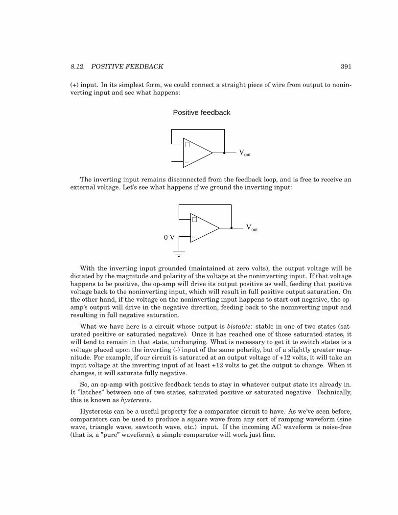
8.12. POSITIVE FEEDBACK 391
(+) input. In its simplest form, we could connect a straight piece of wire from output to nonin-verting input and see what happens:
−
+
Vout
Positive feedback
The inverting input remains disconnected from the feedback loop, and is free to receive anexternal voltage. Let’s see what happens if we ground the inverting input:
−
+
Vout
0 V
With the inverting input grounded (maintained at zero volts), the output voltage will bedictated by the magnitude and polarity of the voltage at the noninverting input. If that voltagehappens to be positive, the op-amp will drive its output positive as well, feeding that positivevoltage back to the noninverting input, which will result in full positive output saturation. Onthe other hand, if the voltage on the noninverting input happens to start out negative, the op-amp’s output will drive in the negative direction, feeding back to the noninverting input andresulting in full negative saturation.
What we have here is a circuit whose output is bistable: stable in one of two states (sat-urated positive or saturated negative). Once it has reached one of those saturated states, itwill tend to remain in that state, unchanging. What is necessary to get it to switch states is avoltage placed upon the inverting (-) input of the same polarity, but of a slightly greater mag-nitude. For example, if our circuit is saturated at an output voltage of +12 volts, it will take aninput voltage at the inverting input of at least +12 volts to get the output to change. When itchanges, it will saturate fully negative.
So, an op-amp with positive feedback tends to stay in whatever output state its already in.It ”latches” between one of two states, saturated positive or saturated negative. Technically,this is known as hysteresis.
Hysteresis can be a useful property for a comparator circuit to have. As we’ve seen before,comparators can be used to produce a square wave from any sort of ramping waveform (sinewave, triangle wave, sawtooth wave, etc.) input. If the incoming AC waveform is noise-free(that is, a ”pure” waveform), a simple comparator will work just fine.
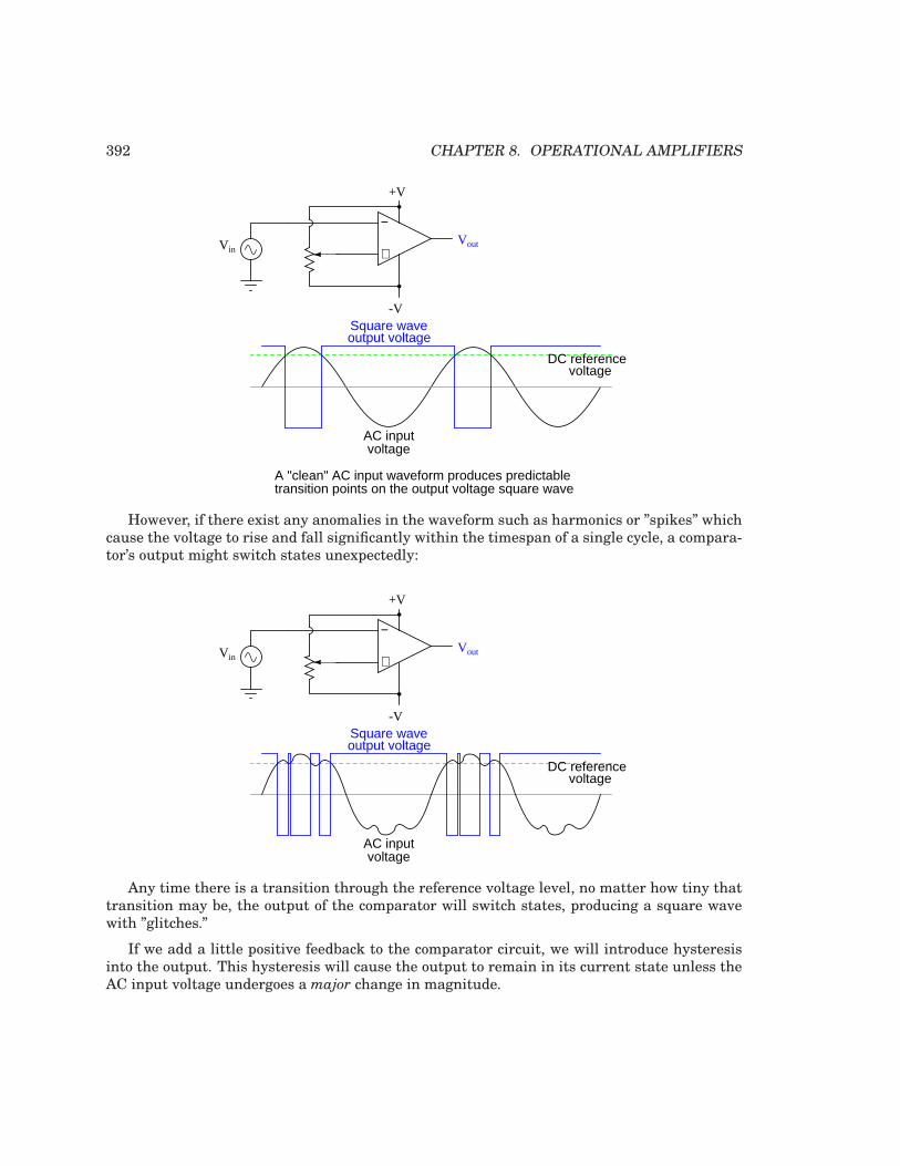
392 CHAPTER 8. OPERATIONAL AMPLIFIERS
−
+
+V
-V
VoutVin
AC inputvoltage
Square waveoutput voltage
DC referencevoltage
A "clean" AC input waveform produces predictabletransition points on the output voltage square wave
However, if there exist any anomalies in the waveform such as harmonics or ”spikes” whichcause the voltage to rise and fall significantly within the timespan of a single cycle, a compara-tor’s output might switch states unexpectedly:
−
+
+V
-V
VoutVin
AC inputvoltage
Square waveoutput voltage
DC referencevoltage
Any time there is a transition through the reference voltage level, no matter how tiny thattransition may be, the output of the comparator will switch states, producing a square wavewith ”glitches.”
If we add a little positive feedback to the comparator circuit, we will introduce hysteresisinto the output. This hysteresis will cause the output to remain in its current state unless theAC input voltage undergoes a major change in magnitude.
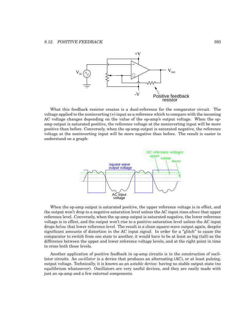
8.12. POSITIVE FEEDBACK 393
−
+
+V
-V
VoutVin
Positive feedbackresistor
What this feedback resistor creates is a dual-reference for the comparator circuit. Thevoltage applied to the noninverting (+) input as a reference which to compare with the incomingAC voltage changes depending on the value of the op-amp’s output voltage. When the op-amp output is saturated positive, the reference voltage at the noninverting input will be morepositive than before. Conversely, when the op-amp output is saturated negative, the referencevoltage at the noninverting input will be more negative than before. The result is easier tounderstand on a graph:
DC reference voltagesupper
centerlower
output voltagesquare wave
AC inputvoltage
When the op-amp output is saturated positive, the upper reference voltage is in effect, andthe output won’t drop to a negative saturation level unless the AC input rises above that upperreference level. Conversely, when the op-amp output is saturated negative, the lower referencevoltage is in effect, and the output won’t rise to a positive saturation level unless the AC inputdrops below that lower reference level. The result is a clean square-wave output again, despitesignificant amounts of distortion in the AC input signal. In order for a ”glitch” to cause thecomparator to switch from one state to another, it would have to be at least as big (tall) as thedifference between the upper and lower reference voltage levels, and at the right point in timeto cross both those levels.
Another application of positive feedback in op-amp circuits is in the construction of oscil-lator circuits. An oscillator is a device that produces an alternating (AC), or at least pulsing,output voltage. Technically, it is known as an astable device: having no stable output state (noequilibrium whatsoever). Oscillators are very useful devices, and they are easily made withjust an op-amp and a few external components.
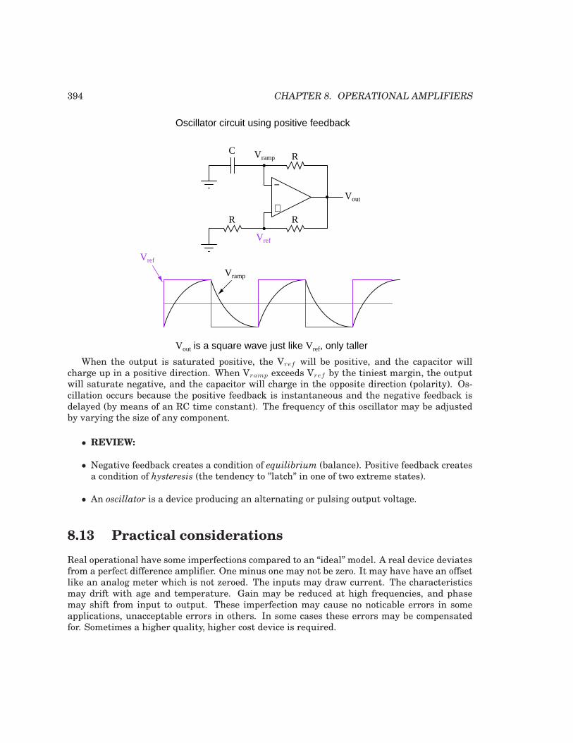
394 CHAPTER 8. OPERATIONAL AMPLIFIERS
−
+Vout
CR
RR
Vramp
Vref
Vref
Vramp
Vout is a square wave just like Vref, only taller
Oscillator circuit using positive feedback
When the output is saturated positive, the Vref will be positive, and the capacitor willcharge up in a positive direction. When Vramp exceeds Vref by the tiniest margin, the outputwill saturate negative, and the capacitor will charge in the opposite direction (polarity). Os-cillation occurs because the positive feedback is instantaneous and the negative feedback isdelayed (by means of an RC time constant). The frequency of this oscillator may be adjustedby varying the size of any component.
• REVIEW:
• Negative feedback creates a condition of equilibrium (balance). Positive feedback createsa condition of hysteresis (the tendency to ”latch” in one of two extreme states).
• An oscillator is a device producing an alternating or pulsing output voltage.
8.13 Practical considerations
Real operational have some imperfections compared to an “ideal” model. A real device deviatesfrom a perfect difference amplifier. One minus one may not be zero. It may have have an offsetlike an analog meter which is not zeroed. The inputs may draw current. The characteristicsmay drift with age and temperature. Gain may be reduced at high frequencies, and phasemay shift from input to output. These imperfection may cause no noticable errors in someapplications, unacceptable errors in others. In some cases these errors may be compensatedfor. Sometimes a higher quality, higher cost device is required.
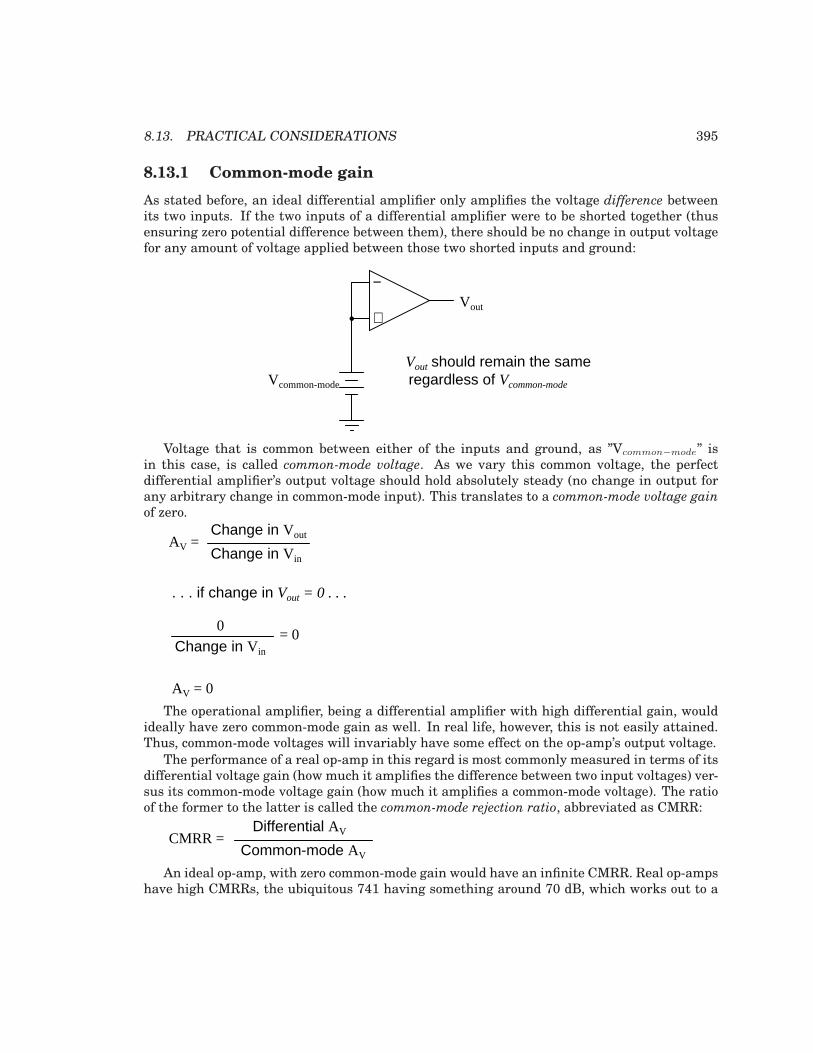
8.13. PRACTICAL CONSIDERATIONS 395
8.13.1 Common-mode gain
As stated before, an ideal differential amplifier only amplifies the voltage difference betweenits two inputs. If the two inputs of a differential amplifier were to be shorted together (thusensuring zero potential difference between them), there should be no change in output voltagefor any amount of voltage applied between those two shorted inputs and ground:
−
+Vout
Vcommon-mode
Vout should remain the sameregardless of Vcommon-mode
Voltage that is common between either of the inputs and ground, as ”Vcommon−mode” isin this case, is called common-mode voltage. As we vary this common voltage, the perfectdifferential amplifier’s output voltage should hold absolutely steady (no change in output forany arbitrary change in common-mode input). This translates to a common-mode voltage gain
of zero.
AV =Change in Vout
Change in Vin
Change in Vin
0= 0
. . . if change in Vout = 0 . . .
AV = 0
The operational amplifier, being a differential amplifier with high differential gain, wouldideally have zero common-mode gain as well. In real life, however, this is not easily attained.Thus, common-mode voltages will invariably have some effect on the op-amp’s output voltage.
The performance of a real op-amp in this regard is most commonly measured in terms of itsdifferential voltage gain (how much it amplifies the difference between two input voltages) ver-sus its common-mode voltage gain (how much it amplifies a common-mode voltage). The ratioof the former to the latter is called the common-mode rejection ratio, abbreviated as CMRR:
CMRR = Differential AV
Common-mode AV
An ideal op-amp, with zero common-mode gain would have an infinite CMRR. Real op-ampshave high CMRRs, the ubiquitous 741 having something around 70 dB, which works out to a
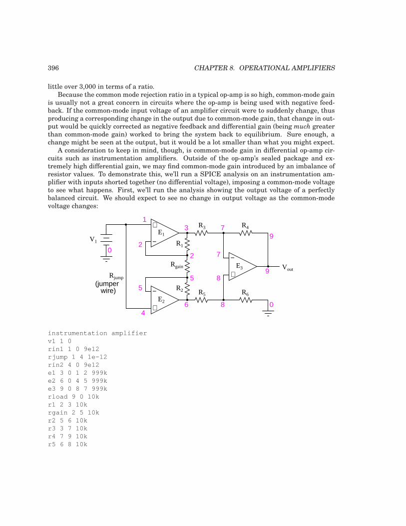
396 CHAPTER 8. OPERATIONAL AMPLIFIERS
little over 3,000 in terms of a ratio.Because the common mode rejection ratio in a typical op-amp is so high, common-mode gain
is usually not a great concern in circuits where the op-amp is being used with negative feed-back. If the common-mode input voltage of an amplifier circuit were to suddenly change, thusproducing a corresponding change in the output due to common-mode gain, that change in out-put would be quickly corrected as negative feedback and differential gain (being much greaterthan common-mode gain) worked to bring the system back to equilibrium. Sure enough, achange might be seen at the output, but it would be a lot smaller than what you might expect.
A consideration to keep in mind, though, is common-mode gain in differential op-amp cir-cuits such as instrumentation amplifiers. Outside of the op-amp’s sealed package and ex-tremely high differential gain, we may find common-mode gain introduced by an imbalance ofresistor values. To demonstrate this, we’ll run a SPICE analysis on an instrumentation am-plifier with inputs shorted together (no differential voltage), imposing a common-mode voltageto see what happens. First, we’ll run the analysis showing the output voltage of a perfectlybalanced circuit. We should expect to see no change in output voltage as the common-modevoltage changes:
−
+
V1
Vout
−
+
−
+
Rgain
3
2
R1
R2
2
1
5
6
5
4
7
8
8
7
9
9
0
E1
E2
E3
R3 R4
R5 R6
0
Rjump
(jumperwire)
instrumentation amplifierv1 1 0rin1 1 0 9e12rjump 1 4 1e-12rin2 4 0 9e12e1 3 0 1 2 999ke2 6 0 4 5 999ke3 9 0 8 7 999krload 9 0 10kr1 2 3 10krgain 2 5 10kr2 5 6 10kr3 3 7 10kr4 7 9 10kr5 6 8 10k
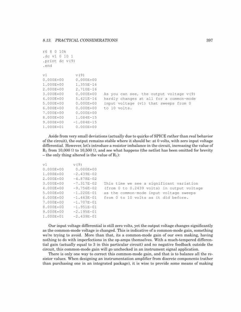
8.13. PRACTICAL CONSIDERATIONS 397
r6 8 0 10k.dc v1 0 10 1.print dc v(9).end
v1 v(9)0.000E+00 0.000E+001.000E+00 1.355E-162.000E+00 2.710E-163.000E+00 0.000E+00 As you can see, the output voltage v(9)4.000E+00 5.421E-16 hardly changes at all for a common-mode5.000E+00 0.000E+00 input voltage (v1) that sweeps from 06.000E+00 0.000E+00 to 10 volts.7.000E+00 0.000E+008.000E+00 1.084E-159.000E+00 -1.084E-151.000E+01 0.000E+00
Aside from very small deviations (actually due to quirks of SPICE rather than real behaviorof the circuit), the output remains stable where it should be: at 0 volts, with zero input voltagedifferential. However, let’s introduce a resistor imbalance in the circuit, increasing the value ofR5 from 10,000 Ω to 10,500 Ω, and see what happens (the netlist has been omitted for brevity– the only thing altered is the value of R5):
v1 v(9)0.000E+00 0.000E+001.000E+00 -2.439E-022.000E+00 -4.878E-023.000E+00 -7.317E-02 This time we see a significant variati on4.000E+00 -9.756E-02 (from 0 to 0.2439 volts) in output volt age5.000E+00 -1.220E-01 as the common-mode input voltage swee ps6.000E+00 -1.463E-01 from 0 to 10 volts as it did before.7.000E+00 -1.707E-018.000E+00 -1.951E-019.000E+00 -2.195E-011.000E+01 -2.439E-01
Our input voltage differential is still zero volts, yet the output voltage changes significantlyas the common-mode voltage is changed. This is indicative of a common-mode gain, somethingwe’re trying to avoid. More than that, its a common-mode gain of our own making, havingnothing to do with imperfections in the op-amps themselves. With a much-tempered differen-tial gain (actually equal to 3 in this particular circuit) and no negative feedback outside thecircuit, this common-mode gain will go unchecked in an instrument signal application.
There is only one way to correct this common-mode gain, and that is to balance all the re-sistor values. When designing an instrumentation amplifier from discrete components (ratherthan purchasing one in an integrated package), it is wise to provide some means of making
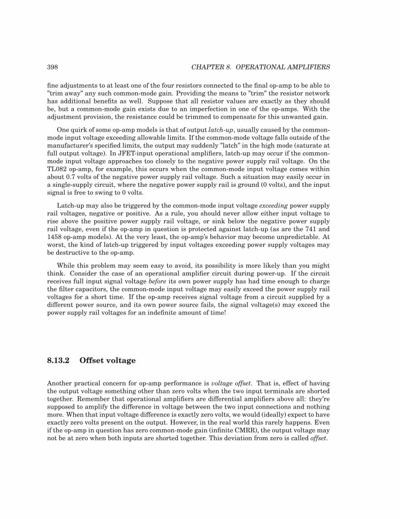
398 CHAPTER 8. OPERATIONAL AMPLIFIERS
fine adjustments to at least one of the four resistors connected to the final op-amp to be able to”trim away” any such common-mode gain. Providing the means to ”trim” the resistor networkhas additional benefits as well. Suppose that all resistor values are exactly as they shouldbe, but a common-mode gain exists due to an imperfection in one of the op-amps. With theadjustment provision, the resistance could be trimmed to compensate for this unwanted gain.
One quirk of some op-amp models is that of output latch-up, usually caused by the common-mode input voltage exceeding allowable limits. If the common-mode voltage falls outside of themanufacturer’s specified limits, the output may suddenly ”latch” in the high mode (saturate atfull output voltage). In JFET-input operational amplifiers, latch-up may occur if the common-mode input voltage approaches too closely to the negative power supply rail voltage. On theTL082 op-amp, for example, this occurs when the common-mode input voltage comes withinabout 0.7 volts of the negative power supply rail voltage. Such a situation may easily occur ina single-supply circuit, where the negative power supply rail is ground (0 volts), and the inputsignal is free to swing to 0 volts.
Latch-up may also be triggered by the common-mode input voltage exceeding power supplyrail voltages, negative or positive. As a rule, you should never allow either input voltage torise above the positive power supply rail voltage, or sink below the negative power supplyrail voltage, even if the op-amp in question is protected against latch-up (as are the 741 and1458 op-amp models). At the very least, the op-amp’s behavior may become unpredictable. Atworst, the kind of latch-up triggered by input voltages exceeding power supply voltages maybe destructive to the op-amp.
While this problem may seem easy to avoid, its possibility is more likely than you mightthink. Consider the case of an operational amplifier circuit during power-up. If the circuitreceives full input signal voltage before its own power supply has had time enough to chargethe filter capacitors, the common-mode input voltage may easily exceed the power supply railvoltages for a short time. If the op-amp receives signal voltage from a circuit supplied by adifferent power source, and its own power source fails, the signal voltage(s) may exceed thepower supply rail voltages for an indefinite amount of time!
8.13.2 Offset voltage
Another practical concern for op-amp performance is voltage offset. That is, effect of havingthe output voltage something other than zero volts when the two input terminals are shortedtogether. Remember that operational amplifiers are differential amplifiers above all: they’resupposed to amplify the difference in voltage between the two input connections and nothingmore. When that input voltage difference is exactly zero volts, we would (ideally) expect to haveexactly zero volts present on the output. However, in the real world this rarely happens. Evenif the op-amp in question has zero common-mode gain (infinite CMRR), the output voltage maynot be at zero when both inputs are shorted together. This deviation from zero is called offset.
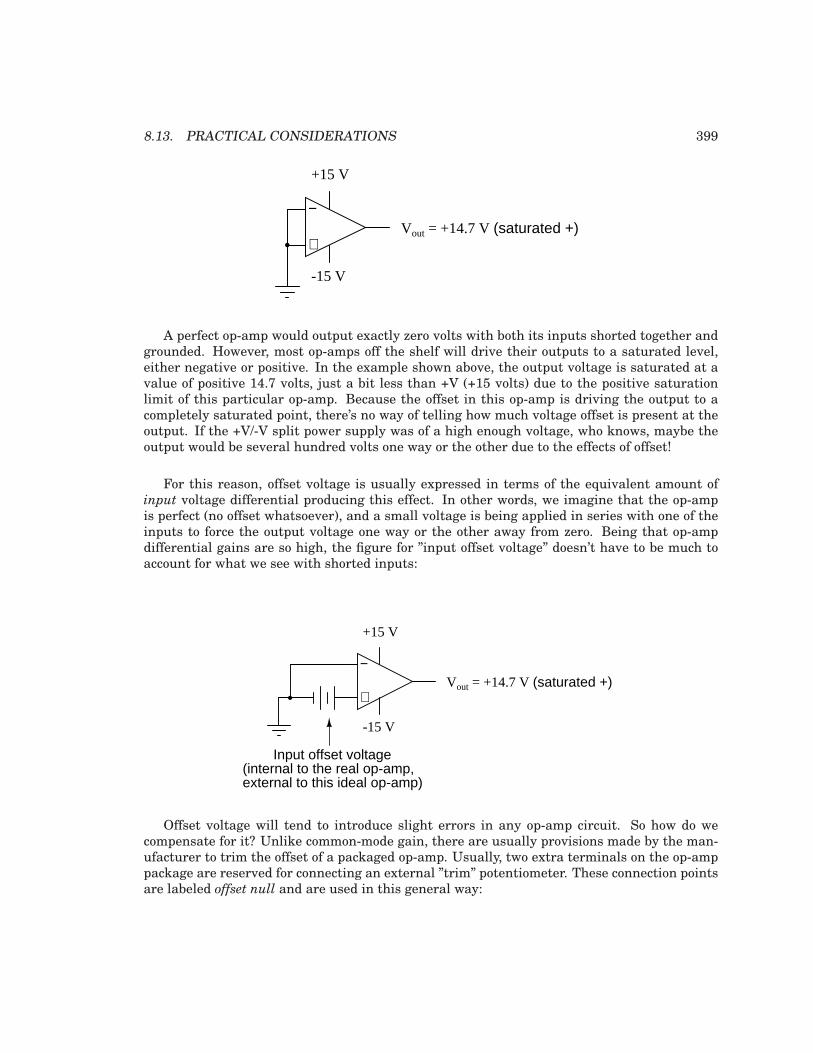
8.13. PRACTICAL CONSIDERATIONS 399
−
+
+15 V
-15 V
Vout = +14.7 V (saturated +)
A perfect op-amp would output exactly zero volts with both its inputs shorted together andgrounded. However, most op-amps off the shelf will drive their outputs to a saturated level,either negative or positive. In the example shown above, the output voltage is saturated at avalue of positive 14.7 volts, just a bit less than +V (+15 volts) due to the positive saturationlimit of this particular op-amp. Because the offset in this op-amp is driving the output to acompletely saturated point, there’s no way of telling how much voltage offset is present at theoutput. If the +V/-V split power supply was of a high enough voltage, who knows, maybe theoutput would be several hundred volts one way or the other due to the effects of offset!
For this reason, offset voltage is usually expressed in terms of the equivalent amount ofinput voltage differential producing this effect. In other words, we imagine that the op-ampis perfect (no offset whatsoever), and a small voltage is being applied in series with one of theinputs to force the output voltage one way or the other away from zero. Being that op-ampdifferential gains are so high, the figure for ”input offset voltage” doesn’t have to be much toaccount for what we see with shorted inputs:
−
+
+15 V
-15 V
Vout = +14.7 V (saturated +)
Input offset voltage(internal to the real op-amp,external to this ideal op-amp)
Offset voltage will tend to introduce slight errors in any op-amp circuit. So how do wecompensate for it? Unlike common-mode gain, there are usually provisions made by the man-ufacturer to trim the offset of a packaged op-amp. Usually, two extra terminals on the op-amppackage are reserved for connecting an external ”trim” potentiometer. These connection pointsare labeled offset null and are used in this general way:
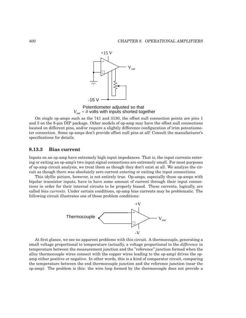
400 CHAPTER 8. OPERATIONAL AMPLIFIERS
−
+
Potentiometer adjusted so thatVout = 0 volts with inputs shorted together
Vout
+15 V
-15 V
On single op-amps such as the 741 and 3130, the offset null connection points are pins 1and 5 on the 8-pin DIP package. Other models of op-amp may have the offset null connectionslocated on different pins, and/or require a slightly difference configuration of trim potentiome-ter connection. Some op-amps don’t provide offset null pins at all! Consult the manufacturer’sspecifications for details.
8.13.3 Bias current
Inputs on an op-amp have extremely high input impedances. That is, the input currents enter-ing or exiting an op-amp’s two input signal connections are extremely small. For most purposesof op-amp circuit analysis, we treat them as though they don’t exist at all. We analyze the cir-cuit as though there was absolutely zero current entering or exiting the input connections.
This idyllic picture, however, is not entirely true. Op-amps, especially those op-amps withbipolar transistor inputs, have to have some amount of current through their input connec-tions in order for their internal circuits to be properly biased. These currents, logically, arecalled bias currents. Under certain conditions, op-amp bias currents may be problematic. Thefollowing circuit illustrates one of those problem conditions:
−
+Thermocouple Vout
+V
-V
At first glance, we see no apparent problems with this circuit. A thermocouple, generating asmall voltage proportional to temperature (actually, a voltage proportional to the difference intemperature between the measurement junction and the ”reference” junction formed when thealloy thermocouple wires connect with the copper wires leading to the op-amp) drives the op-amp either positive or negative. In other words, this is a kind of comparator circuit, comparingthe temperature between the end thermocouple junction and the reference junction (near theop-amp). The problem is this: the wire loop formed by the thermocouple does not provide a
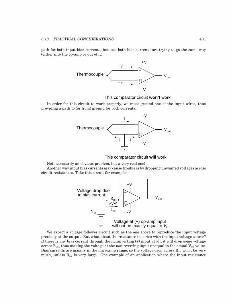
8.13. PRACTICAL CONSIDERATIONS 401
path for both input bias currents, because both bias currents are trying to go the same way(either into the op-amp or out of it).
−
+Thermocouple Vout
+V
-V
I ?
I ?
This comparator circuit won’t workIn order for this circuit to work properly, we must ground one of the input wires, thus
providing a path to (or from) ground for both currents:
−
+Thermocouple Vout
+V
-VI I
I
This comparator circuit will workNot necessarily an obvious problem, but a very real one!Another way input bias currents may cause trouble is by dropping unwanted voltages across
circuit resistances. Take this circuit for example:
−
+Vout
+V
-V
- +Rin
VinIbias
Voltage drop dueto bias current:
Voltage at (+) op-amp inputwill not be exactly equal to Vin
We expect a voltage follower circuit such as the one above to reproduce the input voltageprecisely at the output. But what about the resistance in series with the input voltage source?If there is any bias current through the noninverting (+) input at all, it will drop some voltageacross Rin, thus making the voltage at the noninverting input unequal to the actual Vin value.Bias currents are usually in the microamp range, so the voltage drop across Rin won’t be verymuch, unless Rin is very large. One example of an application where the input resistance
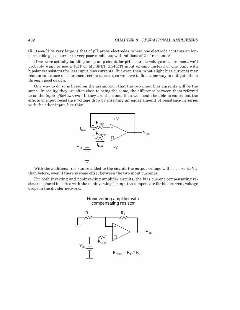
402 CHAPTER 8. OPERATIONAL AMPLIFIERS
(Rin) would be very large is that of pH probe electrodes, where one electrode contains an ion-permeable glass barrier (a very poor conductor, with millions of Ω of resistance).
If we were actually building an op-amp circuit for pH electrode voltage measurement, we’dprobably want to use a FET or MOSFET (IGFET) input op-amp instead of one built withbipolar transistors (for less input bias current). But even then, what slight bias currents mayremain can cause measurement errors to occur, so we have to find some way to mitigate themthrough good design.
One way to do so is based on the assumption that the two input bias currents will be thesame. In reality, they are often close to being the same, the difference between them referredto as the input offset current. If they are the same, then we should be able to cancel out theeffects of input resistance voltage drop by inserting an equal amount of resistance in serieswith the other input, like this:
−
+Vout
+V
-V
- +
VinIbias
Rin(-)
Rin(+)
Ibias
- +
With the additional resistance added to the circuit, the output voltage will be closer to Vin
than before, even if there is some offset between the two input currents.
For both inverting and noninverting amplifier circuits, the bias current compensating re-sistor is placed in series with the noninverting (+) input to compensate for bias current voltagedrops in the divider network:
−
+Vout
Vin
Rcomp
R1 R2
Noninverting amplifier withcompensating resistor
Rcomp = R1 // R2
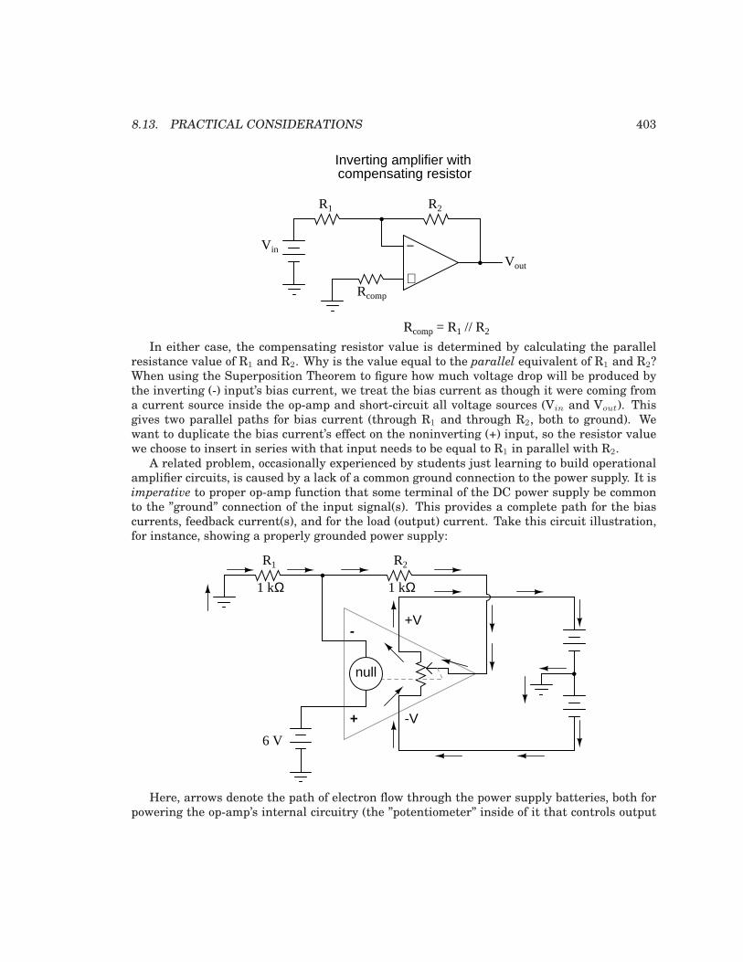
8.13. PRACTICAL CONSIDERATIONS 403
−
+Vout
Vin
Rcomp
R1 R2
compensating resistor
Rcomp = R1 // R2
Inverting amplifier with
In either case, the compensating resistor value is determined by calculating the parallelresistance value of R1 and R2. Why is the value equal to the parallel equivalent of R1 and R2?When using the Superposition Theorem to figure how much voltage drop will be produced bythe inverting (-) input’s bias current, we treat the bias current as though it were coming froma current source inside the op-amp and short-circuit all voltage sources (Vin and Vout). Thisgives two parallel paths for bias current (through R1 and through R2, both to ground). Wewant to duplicate the bias current’s effect on the noninverting (+) input, so the resistor valuewe choose to insert in series with that input needs to be equal to R1 in parallel with R2.
A related problem, occasionally experienced by students just learning to build operationalamplifier circuits, is caused by a lack of a common ground connection to the power supply. It isimperative to proper op-amp function that some terminal of the DC power supply be commonto the ”ground” connection of the input signal(s). This provides a complete path for the biascurrents, feedback current(s), and for the load (output) current. Take this circuit illustration,for instance, showing a properly grounded power supply:
null
-
+
+V
-V
6 V
R1 R2
1 kΩ 1 kΩ
Here, arrows denote the path of electron flow through the power supply batteries, both forpowering the op-amp’s internal circuitry (the ”potentiometer” inside of it that controls output
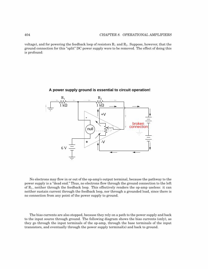
404 CHAPTER 8. OPERATIONAL AMPLIFIERS
voltage), and for powering the feedback loop of resistors R1 and R2. Suppose, however, that theground connection for this ”split” DC power supply were to be removed. The effect of doing thisis profound:
null
-
+
+V
-V
6 V
R1 R2
1 kΩ 1 kΩ
brokenconnection
A power supply ground is essential to circuit operation!
No electrons may flow in or out of the op-amp’s output terminal, because the pathway to thepower supply is a ”dead end.” Thus, no electrons flow through the ground connection to the leftof R1, neither through the feedback loop. This effectively renders the op-amp useless: it canneither sustain current through the feedback loop, nor through a grounded load, since there isno connection from any point of the power supply to ground.
The bias currents are also stopped, because they rely on a path to the power supply and backto the input source through ground. The following diagram shows the bias currents (only), asthey go through the input terminals of the op-amp, through the base terminals of the inputtransistors, and eventually through the power supply terminal(s) and back to ground.
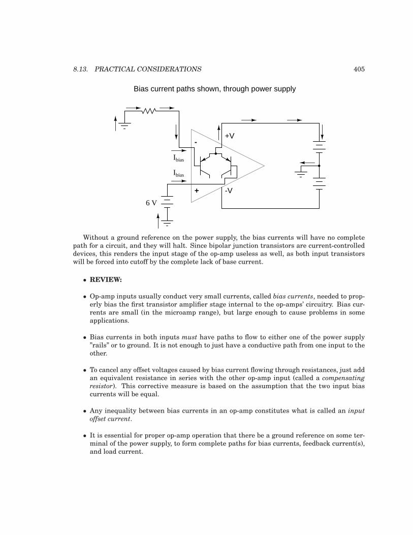
8.13. PRACTICAL CONSIDERATIONS 405
-
+
+V
6 V
Ibias
-V
Ibias
Bias current paths shown, through power supply
Without a ground reference on the power supply, the bias currents will have no completepath for a circuit, and they will halt. Since bipolar junction transistors are current-controlleddevices, this renders the input stage of the op-amp useless as well, as both input transistorswill be forced into cutoff by the complete lack of base current.
• REVIEW:
• Op-amp inputs usually conduct very small currents, called bias currents, needed to prop-erly bias the first transistor amplifier stage internal to the op-amps’ circuitry. Bias cur-rents are small (in the microamp range), but large enough to cause problems in someapplications.
• Bias currents in both inputs must have paths to flow to either one of the power supply”rails” or to ground. It is not enough to just have a conductive path from one input to theother.
• To cancel any offset voltages caused by bias current flowing through resistances, just addan equivalent resistance in series with the other op-amp input (called a compensating
resistor). This corrective measure is based on the assumption that the two input biascurrents will be equal.
• Any inequality between bias currents in an op-amp constitutes what is called an input
offset current.
• It is essential for proper op-amp operation that there be a ground reference on some ter-minal of the power supply, to form complete paths for bias currents, feedback current(s),and load current.
406 CHAPTER 8. OPERATIONAL AMPLIFIERS
8.13.4 Drift
Being semiconductor devices, op-amps are subject to slight changes in behavior with changesin operating temperature. Any changes in op-amp performance with temperature fall underthe category of op-amp drift. Drift parameters can be specified for bias currents, offset voltage,and the like. Consult the manufacturer’s data sheet for specifics on any particular op-amp.
To minimize op-amp drift, we can select an op-amp made to have minimum drift, and/or wecan do our best to keep the operating temperature as stable as possible. The latter action mayinvolve providing some form of temperature control for the inside of the equipment housingthe op-amp(s). This is not as strange as it may first seem. Laboratory-standard precisionvoltage reference generators, for example, are sometimes known to employ ”ovens” for keepingtheir sensitive components (such as zener diodes) at constant temperatures. If extremely highaccuracy is desired over the usual factors of cost and flexibility, this may be an option worthlooking at.
• REVIEW:
• Op-amps, being semiconductor devices, are susceptible to variations in temperature. Anyvariations in amplifier performance resulting from changes in temperature is known asdrift. Drift is best minimized with environmental temperature control.
8.13.5 Frequency response
With their incredibly high differential voltage gains, op-amps are prime candidates for a phe-nomenon known as feedback oscillation. You’ve probably heard the equivalent audio effectwhen the volume (gain) on a public-address or other microphone amplifier system is turnedtoo high: that high pitched squeal resulting from the sound waveform ”feeding back” throughthe microphone to be amplified again. An op-amp circuit can manifest this same effect, withthe feedback happening electrically rather than audibly.
A case example of this is seen in the 3130 op-amp, if it is connected as a voltage followerwith the bare minimum of wiring connections (the two inputs, output, and the power supplyconnections). The output of this op-amp will self-oscillate due to its high gain, no matterwhat the input voltage. To combat this, a small compensation capacitor must be connectedto two specially-provided terminals on the op-amp. The capacitor provides a high-impedancepath for negative feedback to occur within the op-amp’s circuitry, thus decreasing the AC gainand inhibiting unwanted oscillations. If the op-amp is being used to amplify high-frequencysignals, this compensation capacitor may not be needed, but it is absolutely essential for DC orlow-frequency AC signal operation.
Some op-amps, such as the model 741, have a compensation capacitor built in to minimizethe need for external components. This improved simplicity is not without a cost: due to thatcapacitor’s presence inside the op-amp, the negative feedback tends to get stronger as theoperating frequency increases (that capacitor’s reactance decreases with higher frequencies).As a result, the op-amp’s differential voltage gain decreases as frequency goes up: it becomesa less effective amplifier at higher frequencies.
Op-amp manufacturers will publish the frequency response curves for their products. Sincea sufficiently high differential gain is absolutely essential to good feedback operation in op-amp
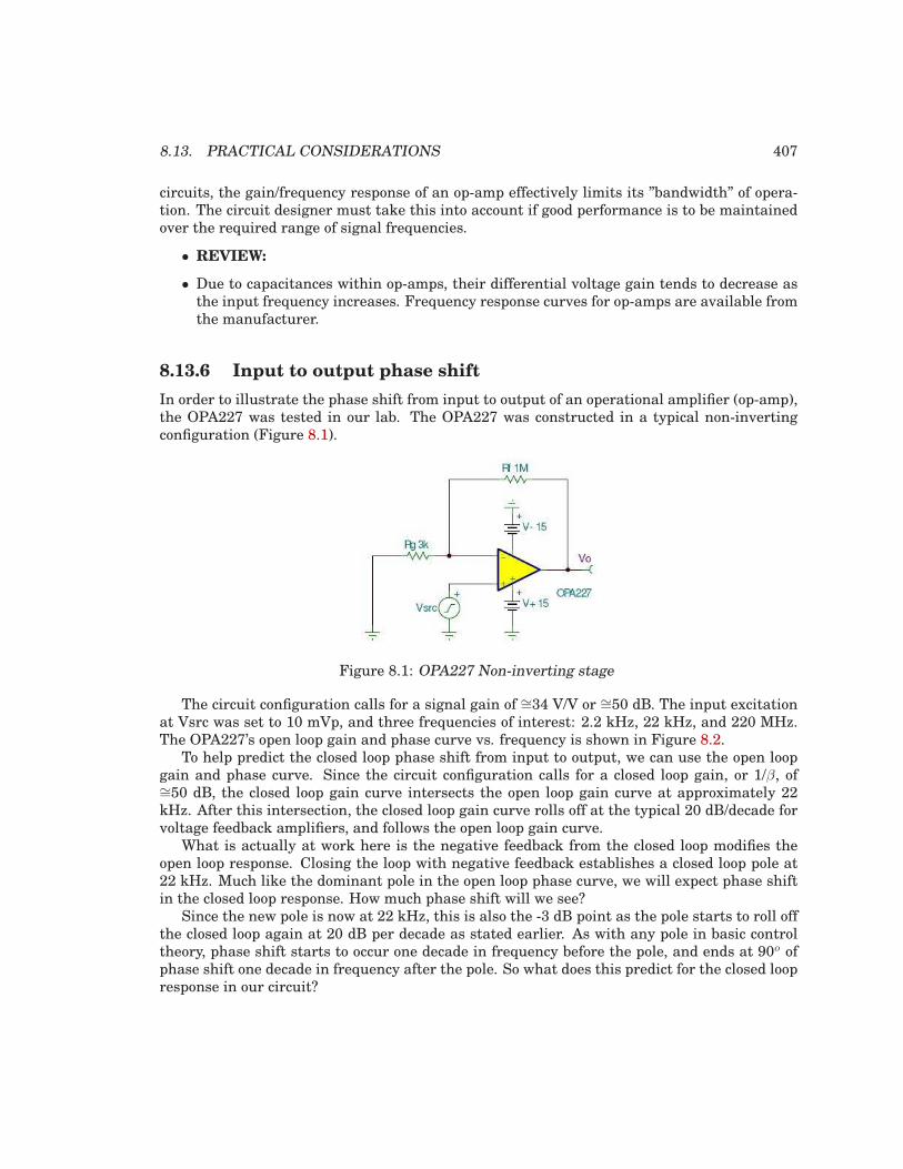
8.13. PRACTICAL CONSIDERATIONS 407
circuits, the gain/frequency response of an op-amp effectively limits its ”bandwidth” of opera-tion. The circuit designer must take this into account if good performance is to be maintainedover the required range of signal frequencies.
• REVIEW:
• Due to capacitances within op-amps, their differential voltage gain tends to decrease asthe input frequency increases. Frequency response curves for op-amps are available fromthe manufacturer.
8.13.6 Input to output phase shift
In order to illustrate the phase shift from input to output of an operational amplifier (op-amp),the OPA227 was tested in our lab. The OPA227 was constructed in a typical non-invertingconfiguration (Figure 8.1).
Figure 8.1: OPA227 Non-inverting stage
The circuit configuration calls for a signal gain of ∼=34 V/V or ∼=50 dB. The input excitationat Vsrc was set to 10 mVp, and three frequencies of interest: 2.2 kHz, 22 kHz, and 220 MHz.The OPA227’s open loop gain and phase curve vs. frequency is shown in Figure 8.2.
To help predict the closed loop phase shift from input to output, we can use the open loopgain and phase curve. Since the circuit configuration calls for a closed loop gain, or 1/β, of∼=50 dB, the closed loop gain curve intersects the open loop gain curve at approximately 22kHz. After this intersection, the closed loop gain curve rolls off at the typical 20 dB/decade forvoltage feedback amplifiers, and follows the open loop gain curve.
What is actually at work here is the negative feedback from the closed loop modifies theopen loop response. Closing the loop with negative feedback establishes a closed loop pole at22 kHz. Much like the dominant pole in the open loop phase curve, we will expect phase shiftin the closed loop response. How much phase shift will we see?
Since the new pole is now at 22 kHz, this is also the -3 dB point as the pole starts to roll offthe closed loop again at 20 dB per decade as stated earlier. As with any pole in basic controltheory, phase shift starts to occur one decade in frequency before the pole, and ends at 90o ofphase shift one decade in frequency after the pole. So what does this predict for the closed loopresponse in our circuit?
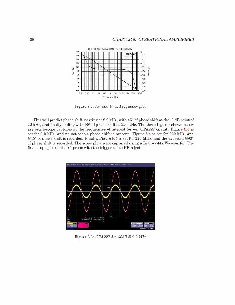
408 CHAPTER 8. OPERATIONAL AMPLIFIERS
Figure 8.2: AV and Φ vs. Frequency plot
This will predict phase shift starting at 2.2 kHz, with 45o of phase shift at the -3 dB point of22 kHz, and finally ending with 90o of phase shift at 220 kHz. The three Figures shown beloware oscilloscope captures at the frequencies of interest for our OPA227 circuit. Figure 8.3 isset for 2.2 kHz, and no noticeable phase shift is present. Figure 8.4 is set for 220 kHz, and∼=45o of phase shift is recorded. Finally, Figure 8.5 is set for 220 MHz, and the expected ∼=90o
of phase shift is recorded. The scope plots were captured using a LeCroy 44x Wavesurfer. Thefinal scope plot used a x1 probe with the trigger set to HF reject.
Figure 8.3: OPA227 Av=50dB @ 2.2 kHz
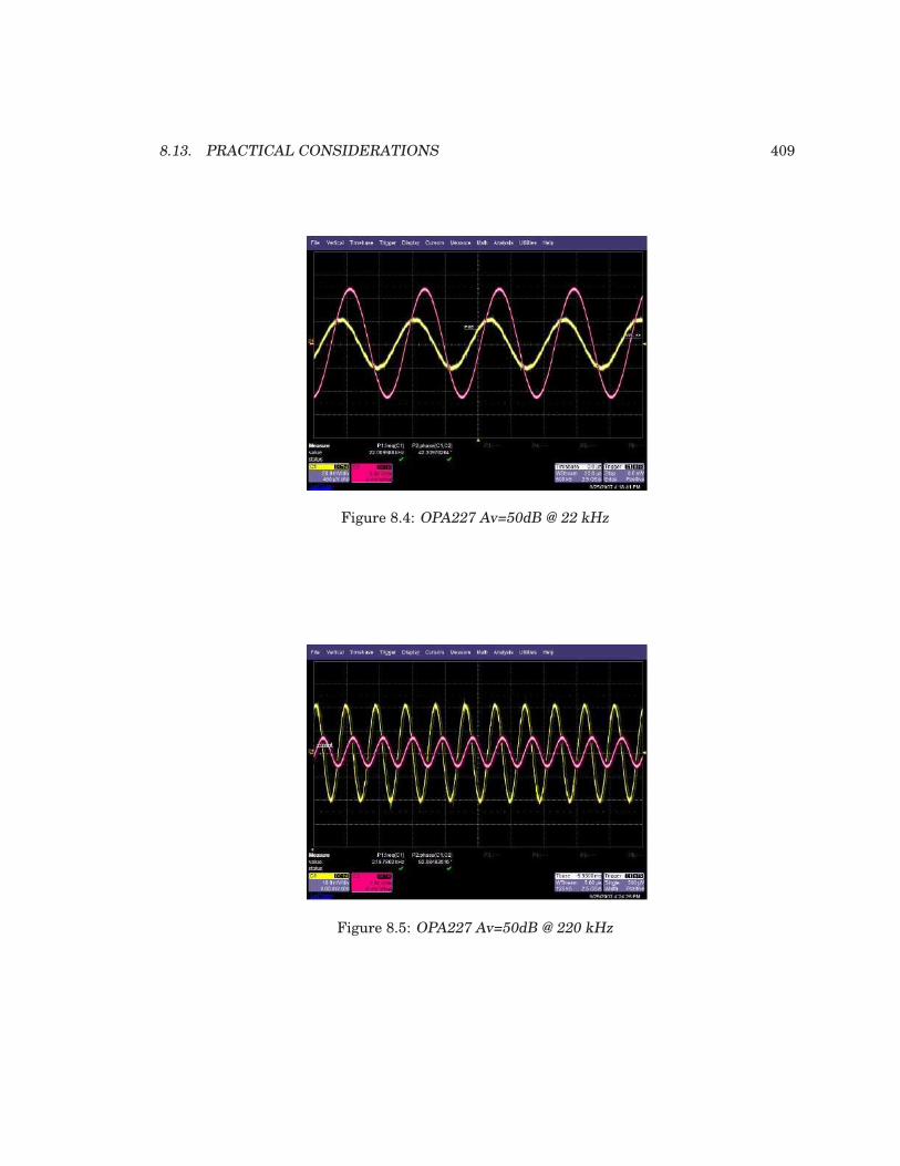
8.13. PRACTICAL CONSIDERATIONS 409
Figure 8.4: OPA227 Av=50dB @ 22 kHz
Figure 8.5: OPA227 Av=50dB @ 220 kHz
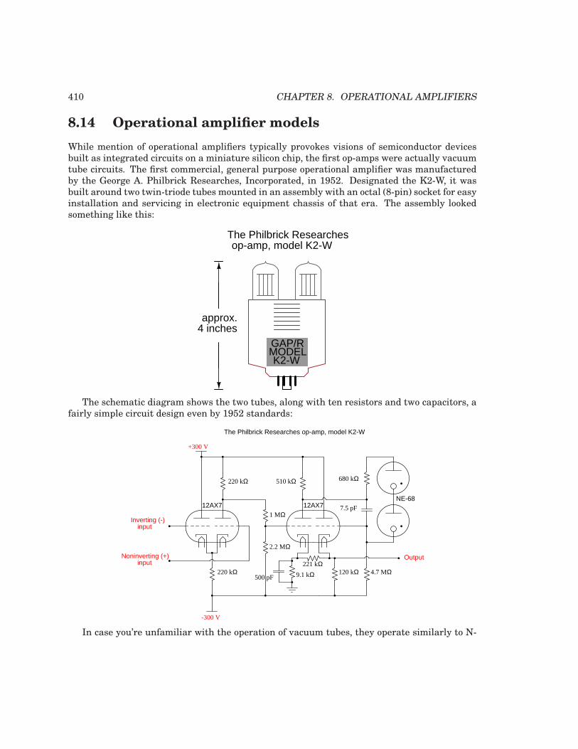
410 CHAPTER 8. OPERATIONAL AMPLIFIERS
8.14 Operational amplifier models
While mention of operational amplifiers typically provokes visions of semiconductor devicesbuilt as integrated circuits on a miniature silicon chip, the first op-amps were actually vacuumtube circuits. The first commercial, general purpose operational amplifier was manufacturedby the George A. Philbrick Researches, Incorporated, in 1952. Designated the K2-W, it wasbuilt around two twin-triode tubes mounted in an assembly with an octal (8-pin) socket for easyinstallation and servicing in electronic equipment chassis of that era. The assembly lookedsomething like this:
The Philbrick Researchesop-amp, model K2-W
GAP/RMODELK2-W
4 inchesapprox.
The schematic diagram shows the two tubes, along with ten resistors and two capacitors, afairly simple circuit design even by 1952 standards:
12AX7
+300 V
220 kΩ
220 kΩ
-300 V
Inverting (-)input
Noninverting (+)input
1 MΩ
2.2 MΩ
510 kΩ
120 kΩ 4.7 MΩ221 kΩ
9.1 kΩ
12AX7
680 kΩ
7.5 pF
500 pF
NE-68
Output
The Philbrick Researches op-amp, model K2-W
In case you’re unfamiliar with the operation of vacuum tubes, they operate similarly to N-
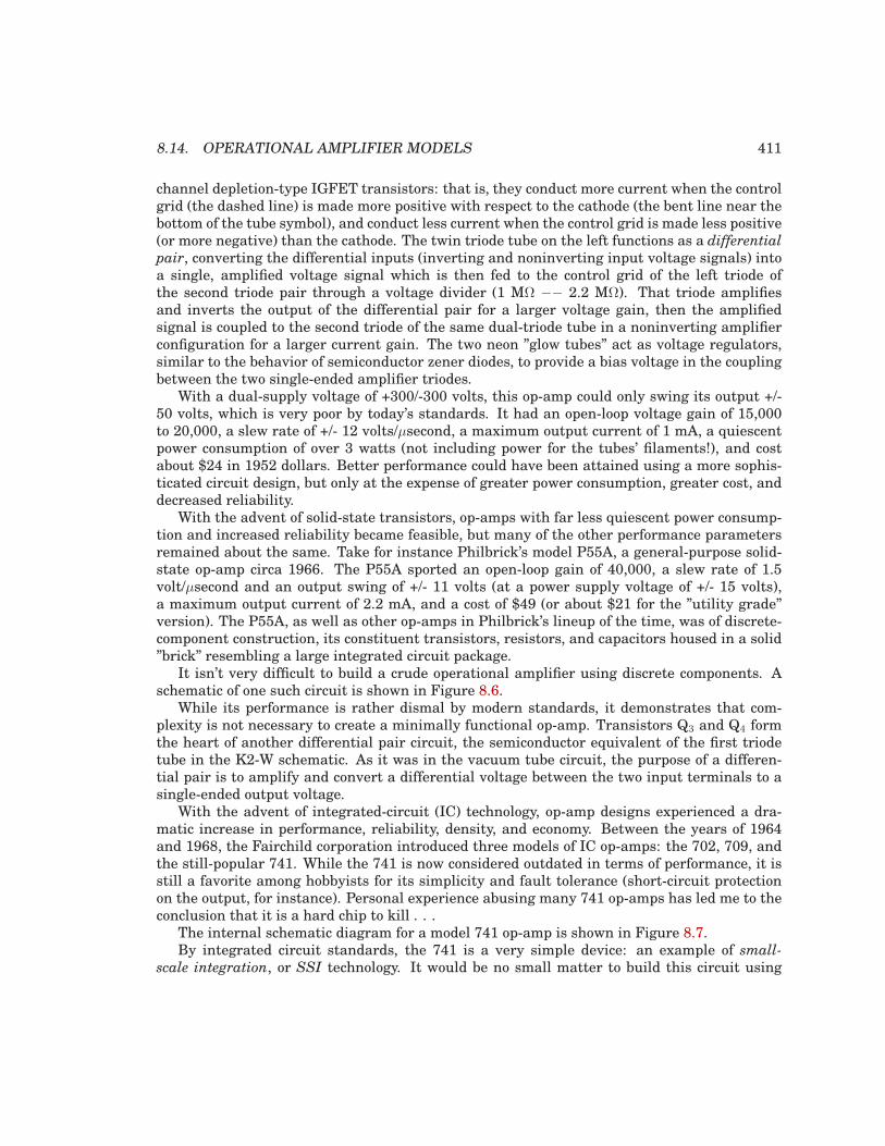
8.14. OPERATIONAL AMPLIFIER MODELS 411
channel depletion-type IGFET transistors: that is, they conduct more current when the controlgrid (the dashed line) is made more positive with respect to the cathode (the bent line near thebottom of the tube symbol), and conduct less current when the control grid is made less positive(or more negative) than the cathode. The twin triode tube on the left functions as a differential
pair, converting the differential inputs (inverting and noninverting input voltage signals) intoa single, amplified voltage signal which is then fed to the control grid of the left triode ofthe second triode pair through a voltage divider (1 MΩ −− 2.2 MΩ). That triode amplifiesand inverts the output of the differential pair for a larger voltage gain, then the amplifiedsignal is coupled to the second triode of the same dual-triode tube in a noninverting amplifierconfiguration for a larger current gain. The two neon ”glow tubes” act as voltage regulators,similar to the behavior of semiconductor zener diodes, to provide a bias voltage in the couplingbetween the two single-ended amplifier triodes.
With a dual-supply voltage of +300/-300 volts, this op-amp could only swing its output +/-50 volts, which is very poor by today’s standards. It had an open-loop voltage gain of 15,000to 20,000, a slew rate of +/- 12 volts/µsecond, a maximum output current of 1 mA, a quiescentpower consumption of over 3 watts (not including power for the tubes’ filaments!), and costabout $24 in 1952 dollars. Better performance could have been attained using a more sophis-ticated circuit design, but only at the expense of greater power consumption, greater cost, anddecreased reliability.
With the advent of solid-state transistors, op-amps with far less quiescent power consump-tion and increased reliability became feasible, but many of the other performance parametersremained about the same. Take for instance Philbrick’s model P55A, a general-purpose solid-state op-amp circa 1966. The P55A sported an open-loop gain of 40,000, a slew rate of 1.5volt/µsecond and an output swing of +/- 11 volts (at a power supply voltage of +/- 15 volts),a maximum output current of 2.2 mA, and a cost of $49 (or about $21 for the ”utility grade”version). The P55A, as well as other op-amps in Philbrick’s lineup of the time, was of discrete-component construction, its constituent transistors, resistors, and capacitors housed in a solid”brick” resembling a large integrated circuit package.
It isn’t very difficult to build a crude operational amplifier using discrete components. Aschematic of one such circuit is shown in Figure 8.6.
While its performance is rather dismal by modern standards, it demonstrates that com-plexity is not necessary to create a minimally functional op-amp. Transistors Q3 and Q4 formthe heart of another differential pair circuit, the semiconductor equivalent of the first triodetube in the K2-W schematic. As it was in the vacuum tube circuit, the purpose of a differen-tial pair is to amplify and convert a differential voltage between the two input terminals to asingle-ended output voltage.
With the advent of integrated-circuit (IC) technology, op-amp designs experienced a dra-matic increase in performance, reliability, density, and economy. Between the years of 1964and 1968, the Fairchild corporation introduced three models of IC op-amps: the 702, 709, andthe still-popular 741. While the 741 is now considered outdated in terms of performance, it isstill a favorite among hobbyists for its simplicity and fault tolerance (short-circuit protectionon the output, for instance). Personal experience abusing many 741 op-amps has led me to theconclusion that it is a hard chip to kill . . .
The internal schematic diagram for a model 741 op-amp is shown in Figure 8.7.By integrated circuit standards, the 741 is a very simple device: an example of small-
scale integration, or SSI technology. It would be no small matter to build this circuit using
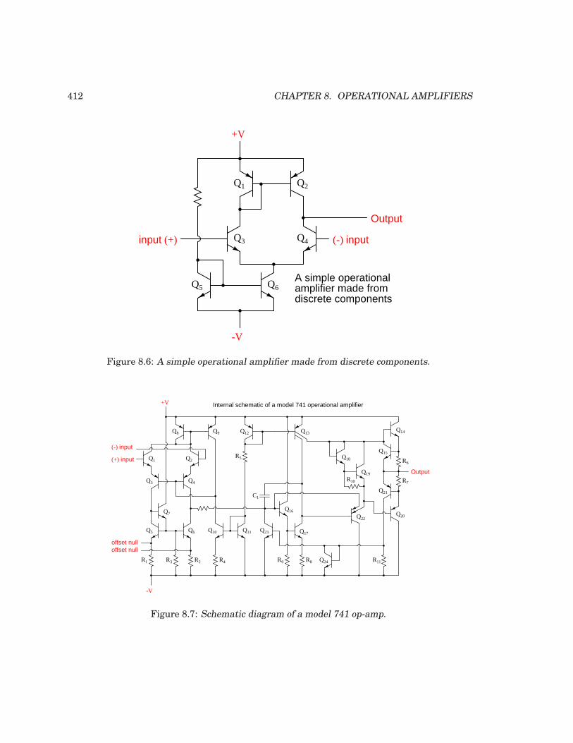
412 CHAPTER 8. OPERATIONAL AMPLIFIERS
Q1 Q2
Q3 Q4
Q5 Q6
-V
+V
(-) inputinput (+)
Output
A simple operationalamplifier made fromdiscrete components
Figure 8.6: A simple operational amplifier made from discrete components.
Q3 Q4
Q1 Q2
Q5 Q6
R1 R2R3 R4
Q7
Q10
Q8 Q9 Q12
Q11
R5(+) input
(-) input
Q13
offset nulloffset null
+V
-V
Q23
Q16
R9 R8
C1
Q17
Q24
Q22
Q19
Q18
R10
Q15
Q14
R6
OutputR7
Q21
Q20
R11
Internal schematic of a model 741 operational amplifier
Figure 8.7: Schematic diagram of a model 741 op-amp.
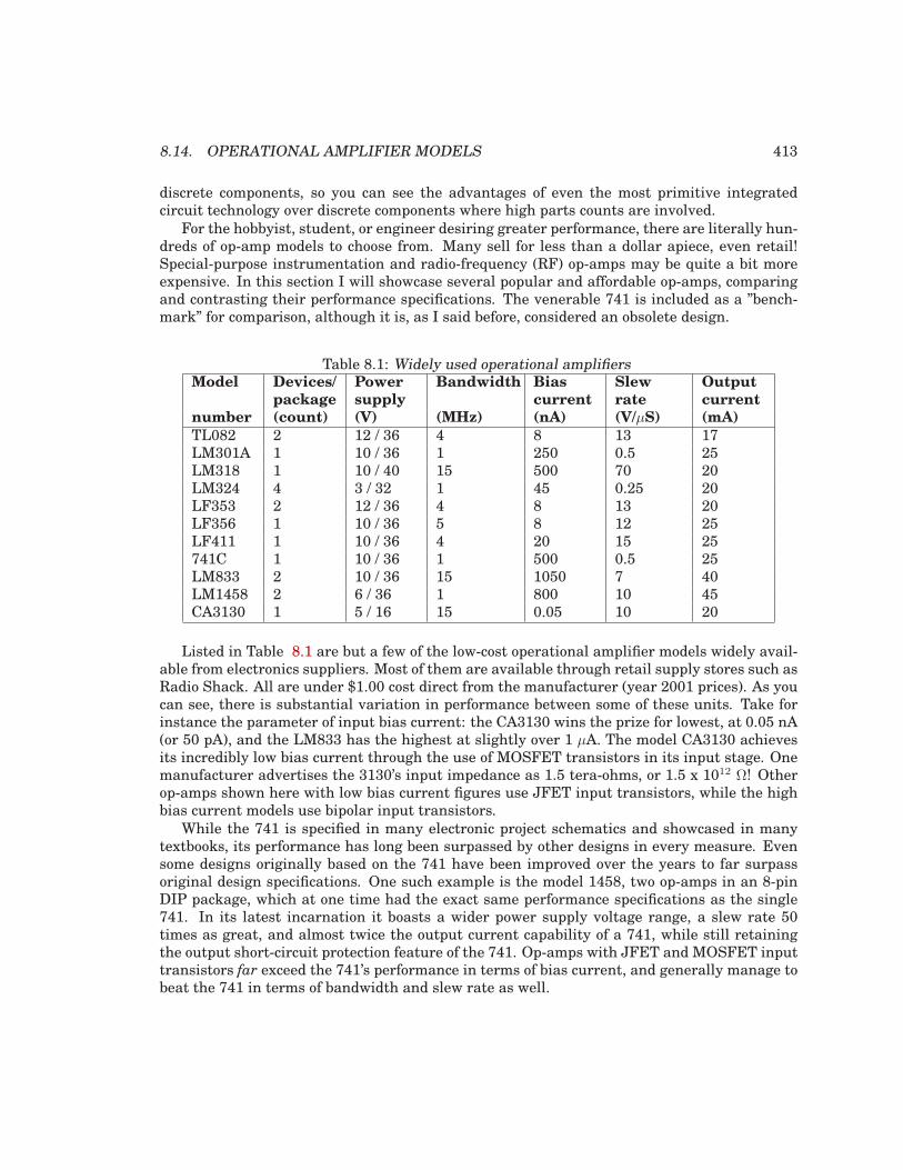
8.14. OPERATIONAL AMPLIFIER MODELS 413
discrete components, so you can see the advantages of even the most primitive integratedcircuit technology over discrete components where high parts counts are involved.
For the hobbyist, student, or engineer desiring greater performance, there are literally hun-dreds of op-amp models to choose from. Many sell for less than a dollar apiece, even retail!Special-purpose instrumentation and radio-frequency (RF) op-amps may be quite a bit moreexpensive. In this section I will showcase several popular and affordable op-amps, comparingand contrasting their performance specifications. The venerable 741 is included as a ”bench-mark” for comparison, although it is, as I said before, considered an obsolete design.
Table 8.1: Widely used operational amplifiersModel Devices/
package
Power
supply
Bandwidth Bias
current
Slew
rate
Output
current
number (count) (V) (MHz) (nA) (V/µS) (mA)
TL082 2 12 / 36 4 8 13 17LM301A 1 10 / 36 1 250 0.5 25LM318 1 10 / 40 15 500 70 20LM324 4 3 / 32 1 45 0.25 20LF353 2 12 / 36 4 8 13 20LF356 1 10 / 36 5 8 12 25LF411 1 10 / 36 4 20 15 25741C 1 10 / 36 1 500 0.5 25LM833 2 10 / 36 15 1050 7 40LM1458 2 6 / 36 1 800 10 45CA3130 1 5 / 16 15 0.05 10 20
Listed in Table 8.1 are but a few of the low-cost operational amplifier models widely avail-able from electronics suppliers. Most of them are available through retail supply stores such asRadio Shack. All are under $1.00 cost direct from the manufacturer (year 2001 prices). As youcan see, there is substantial variation in performance between some of these units. Take forinstance the parameter of input bias current: the CA3130 wins the prize for lowest, at 0.05 nA(or 50 pA), and the LM833 has the highest at slightly over 1 µA. The model CA3130 achievesits incredibly low bias current through the use of MOSFET transistors in its input stage. Onemanufacturer advertises the 3130’s input impedance as 1.5 tera-ohms, or 1.5 x 10¹² Ω! Otherop-amps shown here with low bias current figures use JFET input transistors, while the highbias current models use bipolar input transistors.
While the 741 is specified in many electronic project schematics and showcased in manytextbooks, its performance has long been surpassed by other designs in every measure. Evensome designs originally based on the 741 have been improved over the years to far surpassoriginal design specifications. One such example is the model 1458, two op-amps in an 8-pinDIP package, which at one time had the exact same performance specifications as the single741. In its latest incarnation it boasts a wider power supply voltage range, a slew rate 50times as great, and almost twice the output current capability of a 741, while still retainingthe output short-circuit protection feature of the 741. Op-amps with JFET and MOSFET inputtransistors far exceed the 741’s performance in terms of bias current, and generally manage tobeat the 741 in terms of bandwidth and slew rate as well.
414 CHAPTER 8. OPERATIONAL AMPLIFIERS
My own personal recommendations for op-amps are as such: when low bias current is apriority (such as in low-speed integrator circuits), choose the 3130. For general-purpose DCamplifier work, the 1458 offers good performance (and you get two op-amps in the space ofone package). For an upgrade in performance, choose the model 353, as it is a pin-compatiblereplacement for the 1458. The 353 is designed with JFET input circuitry for very low biascurrent, and has a bandwidth 4 times are great as the 1458, although its output current limitis lower (but still short-circuit protected). It may be more difficult to find on the shelf of yourlocal electronics supply house, but it is just as reasonably priced as the 1458.
If low power supply voltage is a requirement, I recommend the model 324, as it functionson as low as 3 volts DC. Its input bias current requirements are also low, and it provides fourop-amps in a single 14-pin chip. Its major weakness is speed, limited to 1 MHz bandwidth andan output slew rate of only 0.25 volts per µs. For high-frequency AC amplifier circuits, the 318is a very good ”general purpose” model.
Special-purpose op-amps are available for modest cost which provide better performancespecifications. Many of these are tailored for a specific type of performance advantage, such asmaximum bandwidth or minimum bias current. Take for instance the op-amps, both designedfor high bandwidth in Table 8.2.
Table 8.2: High bandwidth operational amplifiersModel Devices/
package
Power
supply
Bandwidth Bias
current
Slew
rate
Output
current
number (count) (V) (MHz) (nA) (V/µS) (mA)
CLC404 1 10 / 14 232 44,000 2600 70CLC425 1 5 / 14 1900 40,000 350 90
The CLC404 lists at $21.80 (almost as much as George Philbrick’s first commercial op-amp, albeit without correction for inflation), while the CLC425 is quite a bit less expensive at$3.23 per unit. In both cases high speed is achieved at the expense of high bias currents andrestrictive power supply voltage ranges. Some op-amps, designed for high power output arelisted in Table 8.3.
Table 8.3: High current operational amplifiersModel Devices/
package
Power
supply
Bandwidth Bias
current
Slew
rate
Output
current
number (count) (V) (MHz) (nA) (V/µS) (mA)
LM12CL 1 15 / 80 0.7 1000 9 13,000LM7171 1 5.5 / 36 200 12,000 4100 100
Yes, the LM12CL actually has an output current rating of 13 amps (13,000 milliamps)!It lists at $14.40, which is not a lot of money, considering the raw power of the device. TheLM7171, on the other hand, trades high current output ability for fast voltage output ability(a high slew rate). It lists at $1.19, about as low as some ”general purpose” op-amps.
Amplifier packages may also be purchased as complete application circuits as opposed tobare operational amplifiers. The Burr-Brown and Analog Devices corporations, for example,
8.15. DATA 415
both long known for their precision amplifier product lines, offer instrumentation amplifiersin pre-designed packages as well as other specialized amplifier devices. In designs where highprecision and repeatability after repair is important, it might be advantageous for the circuitdesigner to choose such a pre-engineered amplifier ”block” rather than build the circuit fromindividual op-amps. Of course, these units typically cost quite a bit more than individual op-amps.
8.15 Data
Parametrical data for all semiconductor op-amp models except the CA3130 comes from Na-tional Semiconductor’s online resources, available at this website: (http://www.national.com) .Data for the CA3130 comes from Harris Semiconductor’s CA3130/CA3130A datasheet (filenumber 817.4).
Contributors
Contributors to this chapter are listed in chronological order of their contributions, from mostrecent to first. See Appendix 2 (Contributor List) for dates and contact information.
Wayne Little (June 2007): Author, “Input to output phase shift” subsection, in “Practicalconsiderations” section.

416 CHAPTER 8. OPERATIONAL AMPLIFIERS
Chapter 9
PRACTICAL ANALOG
SEMICONDUCTOR CIRCUITS
Contents
9.1 ElectroStatic Discharge . . . . . . . . . . . . . . . . . . . . . . . . . . . . . . . 417
9.1.1 ESD Damage Prevention . . . . . . . . . . . . . . . . . . . . . . . . . . . . 418
9.1.2 Storage and Transportation of ESD sensitive component and boards . . . 421
9.1.3 Conclusion . . . . . . . . . . . . . . . . . . . . . . . . . . . . . . . . . . . . 422
9.2 Power supply circuits – INCOMPLETE . . . . . . . . . . . . . . . . . . . . . 422
9.2.1 Unregulated . . . . . . . . . . . . . . . . . . . . . . . . . . . . . . . . . . . 423
9.2.2 Linear regulated . . . . . . . . . . . . . . . . . . . . . . . . . . . . . . . . 423
9.2.3 Switching . . . . . . . . . . . . . . . . . . . . . . . . . . . . . . . . . . . . 423
9.2.4 Ripple regulated . . . . . . . . . . . . . . . . . . . . . . . . . . . . . . . . . 424
9.3 Amplifier circuits – PENDING . . . . . . . . . . . . . . . . . . . . . . . . . . . 424
9.4 Oscillator circuits – INCOMPLETE . . . . . . . . . . . . . . . . . . . . . . . . 424
9.4.1 Varactor multiplier . . . . . . . . . . . . . . . . . . . . . . . . . . . . . . . 424
9.5 Phase-locked loops – PENDING . . . . . . . . . . . . . . . . . . . . . . . . . . 426
9.6 Radio circuits – INCOMPLETE . . . . . . . . . . . . . . . . . . . . . . . . . . 426
9.7 Computational circuits . . . . . . . . . . . . . . . . . . . . . . . . . . . . . . . 435
9.8 Measurement circuits – INCOMPLETE . . . . . . . . . . . . . . . . . . . . . 457
9.9 Control circuits – PENDING . . . . . . . . . . . . . . . . . . . . . . . . . . . . 458
Bibliography . . . . . . . . . . . . . . . . . . . . . . . . . . . . . . . . . . . . . . . . . 458
*** INCOMPLETE ***
9.1 ElectroStatic Discharge
Volume I chapter 1.1 discusses static electricity, and how it is created. This has a lot moresignificance than might be first assumed, as control of static electricity plays a large part in
417
418 CHAPTER 9. PRACTICAL ANALOG SEMICONDUCTOR CIRCUITS
modern electronics and other professions. An ElectroStatic Discharge event is when a staticcharge is bled off in an uncontrolled fashion, and will be referred to as ESD hereafter.
ESD comes in many forms, it can be as small as 50 volts of electricity being equalized upto tens of thousands of volts. The actual power is extremely small, so small that no dangeris generally offered to someone who is in the discharge path of ESD. It usually takes severalthousand volts for a person to even notice ESD in the form of a spark and the familiar zapthat accompanies it. The problem with ESD is even a small discharge that can go completelyunnoticed can ruin semiconductors. A static charge of thousands of volts is common, howeverthe reason it is not a threat is there is no current of any substantial duration behind it. Theseextreme voltages do allow ionization of the air and allow other materials to break down, whichis the root of where the damage comes from.
ESD is not a new problem. Black powder manufacturing and other pyrotechnic industrieshave always been dangerous if an ESD event occurs in the wrong circumstance. During theera of tubes (AKA valves) ESD was a nonexistent issue for electronics, but with the advent ofsemiconductors, and the increase in miniaturization, it has become much more serious.
Damage to components can, and usually do, occur when the part is in the ESD path. Manyparts, such as power diodes, are very robust and can handle the discharge, but if a part hasa small or thin geometry as part of their physical structure then the voltage can break downthat part of the semiconductor. Currents during these events become quite high, but are in thenanosecond to microsecond time frame. Part of the component is left permanently damagedby this, which can cause two types of failure modes. Catastrophic is the easy one, leavingthe part completely nonfunctional. The other can be much more serious. Latent damage mayallow the problem component to work for hours, days or even months after the initial damagebefore catastrophic failure. Many times these parts are referred to as ”walking wounded”, sincethey are working but bad. Figure 9.1 is shown an example of latent (”walking wounded”) ESDdamage. If these components end up in a life support role, such as medical or military use,then the consequences can be grim. For most hobbyists it is an inconvenience, but it can be anexpensive one.
Even components that are considered fairly rugged can be damaged by ESD. Bipolar tran-sistors, the earliest of the solid state amplifiers, are not immune, though less susceptible. Someof the newer high speed components can be ruined with as little as 3 volts. There are compo-nents that might not be considered at risk, such as some specialized resistors and capacitorsmanufactured using MOS (Metal Oxide Semiconductor) technology, that can be damaged viaESD.
9.1.1 ESD Damage Prevention
Before ESD can be prevented it is important to understand what causes it. Generally materialsaround the workbench can be broken up into 3 categories. These are ESD Generative, ESDNeutral, and ESDDissipative (or ESD Conductive). ESDGenerative materials are active staticgenerators, such as most plastics, cat hair, and polyester clothing. ESD Neutral materials aregenerally insulative, but don’t tend to generate or hold static charges very well. Examples ofthis include wood, paper, and cotton. This is not to say they can not be static generators or anESD hazard, but the risk is somewhat minimized by other factors. Wood and wood products,for example, tend to hold moisture, which can make them slightly conductive. This is true ofa lot of organic materials. A highly polished table would not fall under this category, because
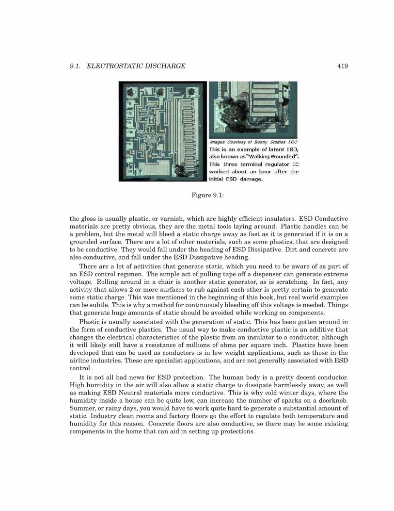
9.1. ELECTROSTATIC DISCHARGE 419
Figure 9.1:
the gloss is usually plastic, or varnish, which are highly efficient insulators. ESD Conductivematerials are pretty obvious, they are the metal tools laying around. Plastic handles can bea problem, but the metal will bleed a static charge away as fast as it is generated if it is on agrounded surface. There are a lot of other materials, such as some plastics, that are designedto be conductive. They would fall under the heading of ESD Dissipative. Dirt and concrete arealso conductive, and fall under the ESD Dissipative heading.
There are a lot of activities that generate static, which you need to be aware of as part ofan ESD control regimen. The simple act of pulling tape off a dispenser can generate extremevoltage. Rolling around in a chair is another static generator, as is scratching. In fact, anyactivity that allows 2 or more surfaces to rub against each other is pretty certain to generatesome static charge. This was mentioned in the beginning of this book, but real world examplescan be subtle. This is why a method for continuously bleeding off this voltage is needed. Thingsthat generate huge amounts of static should be avoided while working on components.
Plastic is usually associated with the generation of static. This has been gotten around inthe form of conductive plastics. The usual way to make conductive plastic is an additive thatchanges the electrical characteristics of the plastic from an insulator to a conductor, althoughit will likely still have a resistance of millions of ohms per square inch. Plastics have beendeveloped that can be used as conductors is in low weight applications, such as those in theairline industries. These are specialist applications, and are not generally associated with ESDcontrol.
It is not all bad news for ESD protection. The human body is a pretty decent conductor.High humidity in the air will also allow a static charge to dissipate harmlessly away, as wellas making ESD Neutral materials more conductive. This is why cold winter days, where thehumidity inside a house can be quite low, can increase the number of sparks on a doorknob.Summer, or rainy days, you would have to work quite hard to generate a substantial amount ofstatic. Industry clean rooms and factory floors go the effort to regulate both temperature andhumidity for this reason. Concrete floors are also conductive, so there may be some existingcomponents in the home that can aid in setting up protections.
420 CHAPTER 9. PRACTICAL ANALOG SEMICONDUCTOR CIRCUITS
To establish ESD protection there has to be a standard voltage level that everything isreferenced to. Such a level exists in the form of ground. There are very good safety reasonsthat ground is used around the house in outlets. In some ways this relates to static, but notdirectly. It does give us a place to dump our excess electrons, or acquire some if we are short,to neutralize any charges our bodies and tools might acquire. If everything on a workbench isconnected directly or indirectly to ground via a conductor then static will dissipate long beforean ESD event has a chance to occur.
A good grounding point can be made several different ways. In houses with modern wiringthat is up to code the ground pin on the AC plug in can be used, or the screw that holds theoutlets cover plate on. This is because house wiring actually has a wire or spike going intothe earth somewhere where the power is tapped from the main power lines. For people whosehouse wiring isn’t quite right a spike driven into the earth at least 3 feet or a simple electricalconnection to metal plumbing (worst option) can be used. The main thing is to establish anelectrical path to the earth outside the house.
Ten megohms is considered a conductor in the world of ESD control. Static electricity isvoltage with no real current, and if a charge is bled off seconds after being generated it isnullified. Generally a 1 to 10 megohm resistor is used to connect any ESD protection for thisreason. It has the benefit of slowing the discharge rate during an ESD event, which increasesthe likelihood of a component surviving undamaged. The faster the discharge, the higher thecurrent spike going though the component. Another reason such a resistance is considereddesirable is if the user is accidentally shorted to high voltage, such as household current, itwon’t be the ESD protections that kill them.
A large industry has grown up around controlling ESD in the electronics industry. Thestaple of any electronics construction is the workbench with a static conductive or dissipativesurface. This surface can be bought commercially, or home made in the form of a sheet of metalor foil. In the case of a metal surface it might be a good idea to lay thin paper on top, although itis not necessary if you are not doing any powered tests on the surface. The commercial versionis usually some form of conductive plastic whose resistance is high enough not to be a problem,which is a better solution. If you are making your own surface for the workbench be sure toadd the 10 megohm resistor to ground, otherwise you have no protection at all.
The other big item that needs ESD grounded is you. People are walking static generators.Your body being conductive it is relatively easy to ground it though, this is usually done witha wrist strap. Commercial versions already have the resistor built in, and have a wide strap tooffer a good contact surface with your skin. Disposable versions can be bought for a few dollars.A metal watchband is also a good ESD protection connection point. Just add a wire (with theresistor) to your grounding point. Most industries take the issue seriously enough to use realtime monitors that will sound an alarm if the operator is not properly grounded.
Another way of grounding yourself is a heel strap. A conductive plastic part is wrappedaround the heel of your shoe, with a conductive plastic strap going up and under your sock forgood contact with the skin. It only works on floors with conductive wax or concrete. The methodwill keep a person from generating large charges that can overwhelm other ESD protections,and is not considered adequate in and of itself. You can get the same effect by walking barefooton a concrete floor.
Yet another ESD protection is to wear ESD conductive smocks. Like the heel strap, this isa secondary protection, not meant to replace the wrist strap. They are meant to short circuitany charges that your clothes may generate.
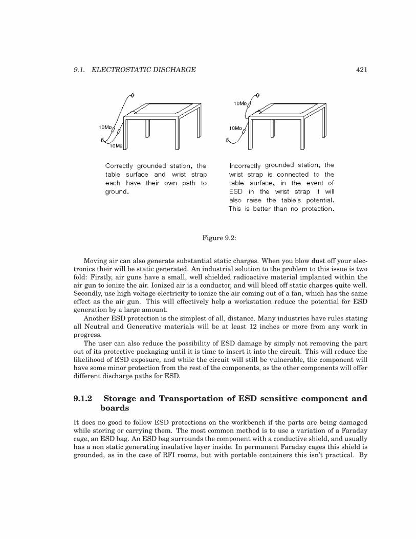
9.1. ELECTROSTATIC DISCHARGE 421
Figure 9.2:
Moving air can also generate substantial static charges. When you blow dust off your elec-tronics their will be static generated. An industrial solution to the problem to this issue is twofold: Firstly, air guns have a small, well shielded radioactive material implanted within theair gun to ionize the air. Ionized air is a conductor, and will bleed off static charges quite well.Secondly, use high voltage electricity to ionize the air coming out of a fan, which has the sameeffect as the air gun. This will effectively help a workstation reduce the potential for ESDgeneration by a large amount.
Another ESD protection is the simplest of all, distance. Many industries have rules statingall Neutral and Generative materials will be at least 12 inches or more from any work inprogress.
The user can also reduce the possibility of ESD damage by simply not removing the partout of its protective packaging until it is time to insert it into the circuit. This will reduce thelikelihood of ESD exposure, and while the circuit will still be vulnerable, the component willhave some minor protection from the rest of the components, as the other components will offerdifferent discharge paths for ESD.
9.1.2 Storage and Transportation of ESD sensitive component andboards
It does no good to follow ESD protections on the workbench if the parts are being damagedwhile storing or carrying them. The most common method is to use a variation of a Faradaycage, an ESD bag. An ESD bag surrounds the component with a conductive shield, and usuallyhas a non static generating insulative layer inside. In permanent Faraday cages this shield isgrounded, as in the case of RFI rooms, but with portable containers this isn’t practical. By
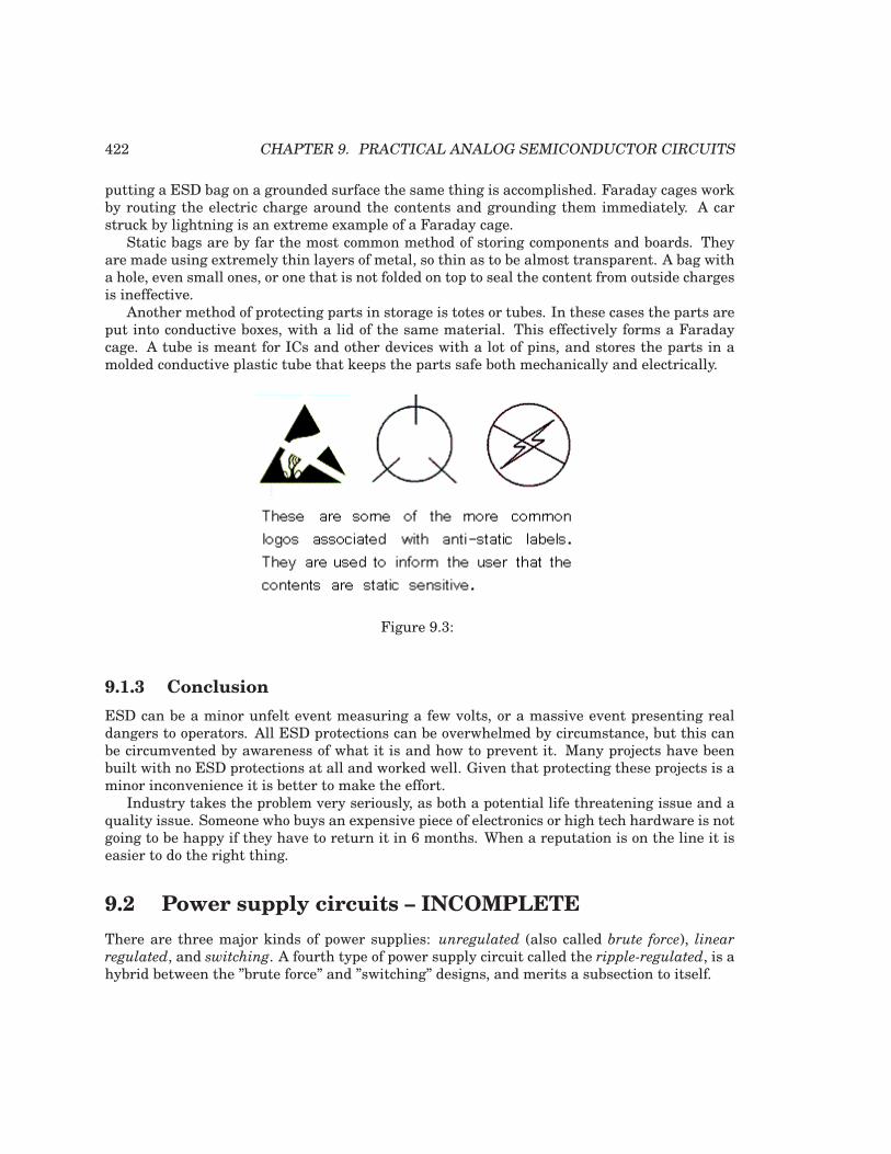
422 CHAPTER 9. PRACTICAL ANALOG SEMICONDUCTOR CIRCUITS
putting a ESD bag on a grounded surface the same thing is accomplished. Faraday cages workby routing the electric charge around the contents and grounding them immediately. A carstruck by lightning is an extreme example of a Faraday cage.
Static bags are by far the most common method of storing components and boards. Theyare made using extremely thin layers of metal, so thin as to be almost transparent. A bag witha hole, even small ones, or one that is not folded on top to seal the content from outside chargesis ineffective.
Another method of protecting parts in storage is totes or tubes. In these cases the parts areput into conductive boxes, with a lid of the same material. This effectively forms a Faradaycage. A tube is meant for ICs and other devices with a lot of pins, and stores the parts in amolded conductive plastic tube that keeps the parts safe both mechanically and electrically.
Figure 9.3:
9.1.3 Conclusion
ESD can be a minor unfelt event measuring a few volts, or a massive event presenting realdangers to operators. All ESD protections can be overwhelmed by circumstance, but this canbe circumvented by awareness of what it is and how to prevent it. Many projects have beenbuilt with no ESD protections at all and worked well. Given that protecting these projects is aminor inconvenience it is better to make the effort.
Industry takes the problem very seriously, as both a potential life threatening issue and aquality issue. Someone who buys an expensive piece of electronics or high tech hardware is notgoing to be happy if they have to return it in 6 months. When a reputation is on the line it iseasier to do the right thing.
9.2 Power supply circuits – INCOMPLETE
There are three major kinds of power supplies: unregulated (also called brute force), linearregulated, and switching. A fourth type of power supply circuit called the ripple-regulated, is ahybrid between the ”brute force” and ”switching” designs, and merits a subsection to itself.
9.2. POWER SUPPLY CIRCUITS – INCOMPLETE 423
9.2.1 Unregulated
An unregulated power supply is the most rudimentary type, consisting of a transformer, rec-tifier, and low-pass filter. These power supplies typically exhibit a lot of ripple voltage (i.e.rapidly-varying instability) and other AC ”noise” superimposed on the DC power. If the inputvoltage varies, the output voltage will vary by a proportional amount. The advantage of anunregulated supply is that its cheap, simple, and efficient.
9.2.2 Linear regulated
A linear regulated supply is simply a ”brute force” (unregulated) power supply followed by atransistor circuit operating in its ”active,” or ”linear” mode, hence the name linear regulator.(Obvious in retrospect, isn’t it?) A typical linear regulator is designed to output a fixed voltagefor a wide range of input voltages, and it simply drops any excess input voltage to allow amaximum output voltage to the load. This excess voltage drop results in significant powerdissipation in the form of heat. If the input voltage gets too low, the transistor circuit will loseregulation, meaning that it will fail to keep the voltage steady. It can only drop excess voltage,not make up for a deficiency in voltage from the brute force section of the circuit. Therefore, youhave to keep the input voltage at least 1 to 3 volts higher than the desired output, dependingon the regulator type. This means the power equivalent of at least 1 to 3 volts multiplied bythe full load current will be dissipated by the regulator circuit, generating a lot of heat. Thismakes linear regulated power supplies rather inefficient. Also, to get rid of all that heat theyhave to use large heat sinks which makes them large, heavy, and expensive.
9.2.3 Switching
A switching regulated power supply (”switcher”) is an effort to realize the advantages of bothbrute force and linear regulated designs (small, efficient, and cheap, but also ”clean,” stableoutput voltage). Switching power supplies work on the principle of rectifying the incoming ACpower line voltage into DC, re-converting it into high-frequency square-wave AC through tran-sistors operated as on/off switches, stepping that AC voltage up or down by using a lightweighttransformer, then rectifying the transformer’s AC output into DC and filtering for final out-put. Voltage regulation is achieved by altering the ”duty cycle” of the DC-to-AC inversion onthe transformer’s primary side. In addition to lighter weight because of a smaller transformercore, switchers have another tremendous advantage over the prior two designs: this type ofpower supply can be made so totally independent of the input voltage that it can work on anyelectric power system in the world; these are called ”universal” power supplies.
The downside of switchers is that they are more complex, and due to their operation theytend to generate a lot of high-frequency AC ”noise” on the power line. Most switchers also havesignificant ripple voltage on their outputs. With the cheaper types, this noise and ripple can beas bad as for an unregulated power supply; such low-end switchers aren’t worthless, becausethey still provide a stable average output voltage, and there’s the ”universal” input capability.
Expensive switchers are ripple-free and have noise nearly as low as for some a linear types;these switchers tend to be as expensive as linear supplies. The reason to use an expensiveswitcher instead of a good linear is if you need universal power system compatibility or high
424 CHAPTER 9. PRACTICAL ANALOG SEMICONDUCTOR CIRCUITS
efficiency. High efficiency, light weight, and small size are the reasons switching power suppliesare almost universally used for powering digital computer circuitry.
9.2.4 Ripple regulated
A ripple-regulated power supply is an alternative to the linear regulated design scheme: a”brute force” power supply (transformer, rectifier, filter) constitutes the ”front end” of the cir-cuit, but a transistor operated strictly in its on/off (saturation/cutoff) modes transfers DC powerto a large capacitor as needed to maintain the output voltage between a high and a low set-point. As in switchers, the transistor in a ripple regulator never passes current while in its”active,” or ”linear,” mode for any substantial length of time, meaning that very little energywill be wasted in the form of heat. However, the biggest drawback to this regulation scheme isthe necessary presence of some ripple voltage on the output, as the DC voltage varies betweenthe two voltage control setpoints. Also, this ripple voltage varies in frequency depending onload current, which makes final filtering of the DC power more difficult.
Ripple regulator circuits tend to be quite a bit simpler than switcher circuitry, and theyneed not handle the high power line voltages that switcher transistors must handle, makingthem safer to work on.
9.3 Amplifier circuits – PENDING
Note, Q3 and Q4 in Figure 9.4 are complementary, NPN and PNP respectively. This circuitworks well for moderate power audio amplifiers. For an explanation of this circuit see “Directcoupled complementary-pair,”
(page 257).
9.4 Oscillator circuits – INCOMPLETE
The phase shift oscillator of Figure 9.5 produces a sinewave output in the audio frequencyrange. Resistive feedback from the collector would be negative feedback due to 180o phasing(base to collector phase inversion). However, the three 60o RC phase shifters ( R1C1, R2C2,and R3C3) provide an additional 180o for a total of 360o. This in-phase feedback constitutespositive feedback. Oscillations result if transistor gain exceeds feedback network losses.
9.4.1 Varactor multiplier
A Varactor or variable capacitance diode with a nonlinear capacitance vs frequency character-istic distorts the applied sinewave f1 in Figure 9.6, generating harmonics, f3.
The fundamental filter passes f1, blocking the harmonics from returning to the generator.The choke passes DC, and blocks radio frequencies (RF) from entering the Vbias supply. Theharmonic filter passes the desired harmonic, say the 3rd, to the output, f3. The capacitor atthe bottom of the inductor is a large value, low reactance, to block DC but ground the inductor
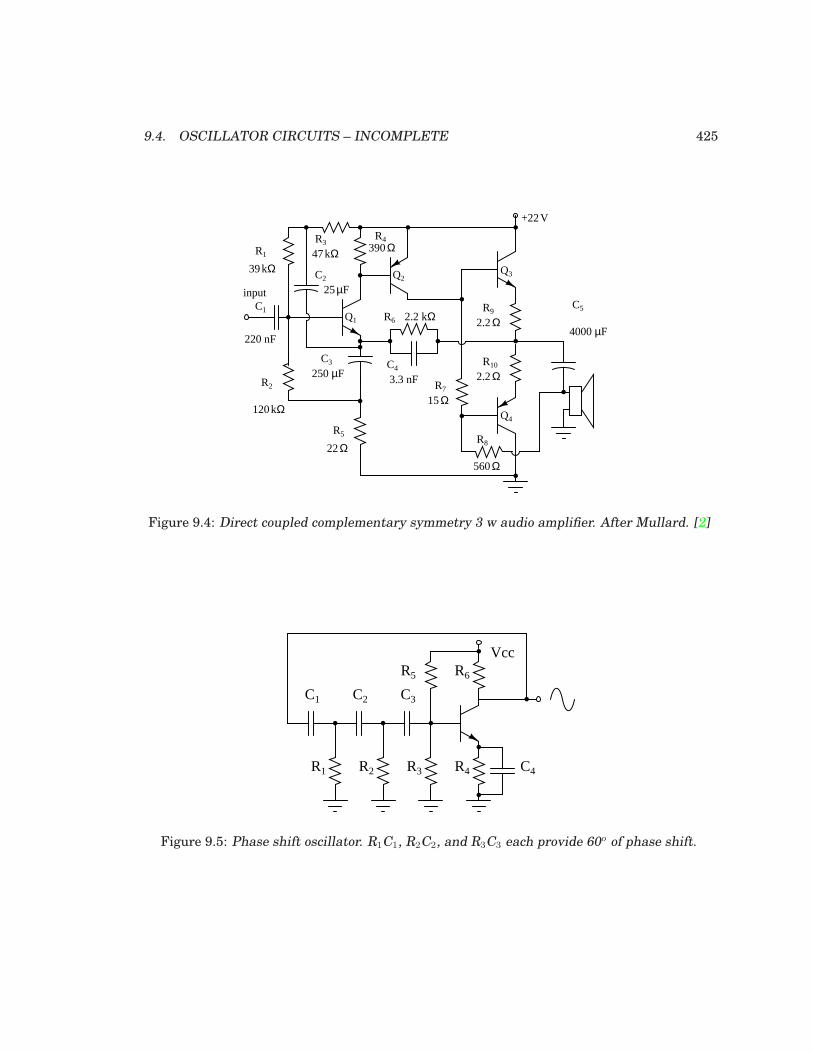
9.4. OSCILLATOR CIRCUITS – INCOMPLETE 425
+22V
input
Q1
Q2Q3
Q4
R6
R8
R3
R2
R5
R7
R4
R1
C5
4000 µF 2.2 kΩ
C4
3.3 nF
R9
R10
2.2Ω
2.2Ω
15Ω
39 kΩ 47kΩ 390Ω
C3
250 µF
C2
25µF
22Ω
560Ω
C1
220 nF
120 kΩ
Figure 9.4: Direct coupled complementary symmetry 3 w audio amplifier. After Mullard. [2]
Vcc
C1 C2 C3
R1 R2 R3 R4
R5 R6
C4
Figure 9.5: Phase shift oscillator. R1C1, R2C2, and R3C3 each provide 60o of phase shift.
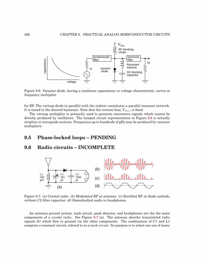
426 CHAPTER 9. PRACTICAL ANALOG SEMICONDUCTOR CIRCUITS
fundamentalfilter
harmonicfilter
Vbias
voltage
capa
cita
nce
RF blockingchoke
f1
f3
DC blockingcapacitor
varactor diode
Resonantinductor
Figure 9.6: Varactor diode, having a nonlinear capacitance vs voltage characteristic, serves infrequency multiplier.
for RF. The varicap diode in parallel with the indctor constitutes a parallel resonant network.It is tuned to the desired harmonic. Note that the reverse bias, Vbias, is fixed.
The varicap multiplier is primarily used to generate microwave signals which cannot bedirectly produced by oscillators. The lumped circuit representation in Figure 9.6 is actuallystripline or waveguide sections. Frequenies up to hundreds of gHzmay be produced by varactormultipliers.
9.5 Phase-locked loops – PENDING
9.6 Radio circuits – INCOMPLETE
C1365pF
C21000pf
L1240µΗ
(a) (d)
(c)
(b)
Figure 9.7: (a) Crystal radio. (b) Modulated RF at antenna. (c) Rectified RF at diode cathode,without C2 filter capacitor. (d) Demodualted audio to headphones.
An antenna ground system, tank circuit, peak detector, and headphones are the the maincomponents of a crystal radio. See Figure 9.7 (a). The antenna absorbs transimtted radiosignals (b) which flow to ground via the other components. The combination of C1 and L1comprise a resonant circuit, refered to as a tank circuit. Its purpose is to select one out of many
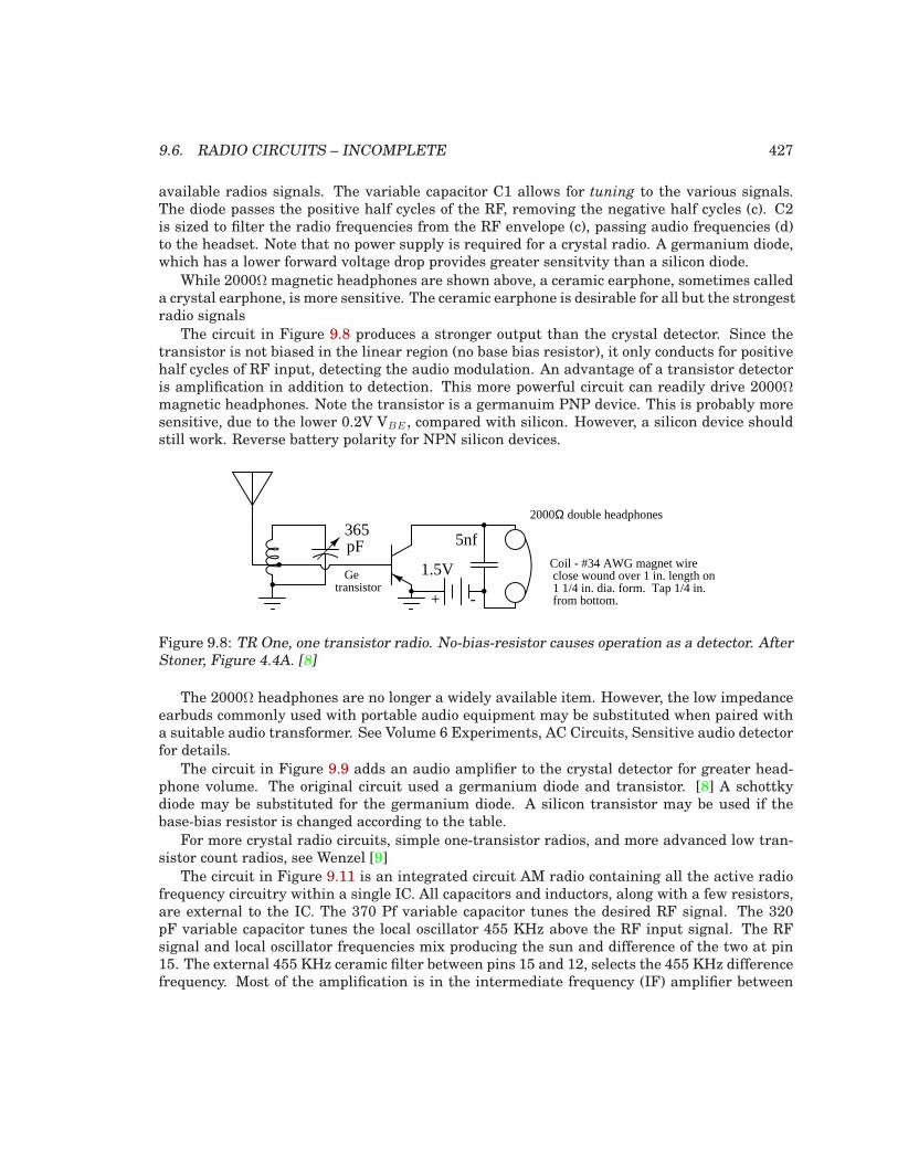
9.6. RADIO CIRCUITS – INCOMPLETE 427
available radios signals. The variable capacitor C1 allows for tuning to the various signals.The diode passes the positive half cycles of the RF, removing the negative half cycles (c). C2is sized to filter the radio frequencies from the RF envelope (c), passing audio frequencies (d)to the headset. Note that no power supply is required for a crystal radio. A germanium diode,which has a lower forward voltage drop provides greater sensitvity than a silicon diode.
While 2000Ω magnetic headphones are shown above, a ceramic earphone, sometimes calleda crystal earphone, is more sensitive. The ceramic earphone is desirable for all but the strongestradio signals
The circuit in Figure 9.8 produces a stronger output than the crystal detector. Since thetransistor is not biased in the linear region (no base bias resistor), it only conducts for positivehalf cycles of RF input, detecting the audio modulation. An advantage of a transistor detectoris amplification in addition to detection. This more powerful circuit can readily drive 2000Ωmagnetic headphones. Note the transistor is a germanuim PNP device. This is probably moresensitive, due to the lower 0.2V VBE , compared with silicon. However, a silicon device shouldstill work. Reverse battery polarity for NPN silicon devices.
5nf
1.5V Coil - #34 AWG magnet wire close wound over 1 in. length on 1 1/4 in. dia. form. Tap 1/4 in. from bottom.
365pF
Getransistor
2000Ω double headphones
-+
Figure 9.8: TR One, one transistor radio. No-bias-resistor causes operation as a detector. AfterStoner, Figure 4.4A. [8]
The 2000Ω headphones are no longer a widely available item. However, the low impedanceearbuds commonly used with portable audio equipment may be substituted when paired witha suitable audio transformer. See Volume 6 Experiments, AC Circuits, Sensitive audio detectorfor details.
The circuit in Figure 9.9 adds an audio amplifier to the crystal detector for greater head-phone volume. The original circuit used a germanium diode and transistor. [8] A schottkydiode may be substituted for the germanium diode. A silicon transistor may be used if thebase-bias resistor is changed according to the table.
For more crystal radio circuits, simple one-transistor radios, and more advanced low tran-sistor count radios, see Wenzel [9]
The circuit in Figure 9.11 is an integrated circuit AM radio containing all the active radiofrequency circuitry within a single IC. All capacitors and inductors, along with a few resistors,are external to the IC. The 370 Pf variable capacitor tunes the desired RF signal. The 320pF variable capacitor tunes the local oscillator 455 KHz above the RF input signal. The RFsignal and local oscillator frequencies mix producing the sun and difference of the two at pin15. The external 455 KHz ceramic filter between pins 15 and 12, selects the 455 KHz differencefrequency. Most of the amplification is in the intermediate frequency (IF) amplifier between
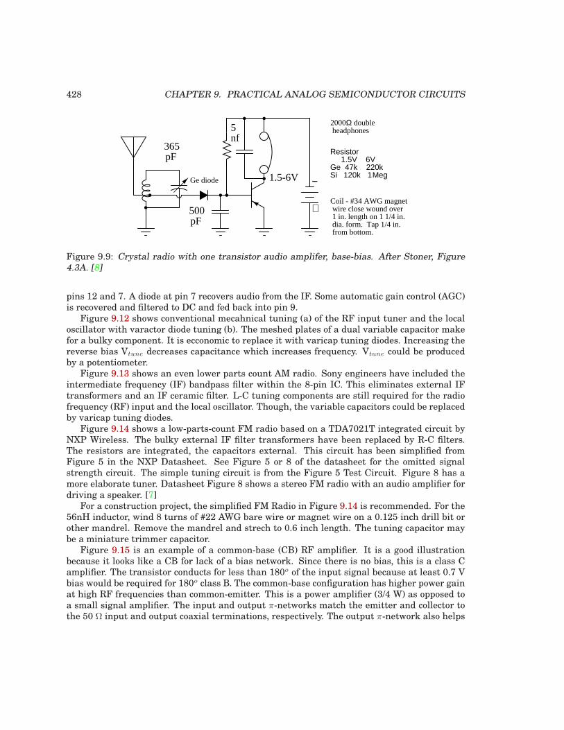
428 CHAPTER 9. PRACTICAL ANALOG SEMICONDUCTOR CIRCUITS
5nf
1.5-6V
Coil - #34 AWG magnet wire close wound over 1 in. length on 1 1/4 in. dia. form. Tap 1/4 in. from bottom.
365pF
Ge diode
2000Ω double headphones
500pF
−
+
Resistor 1.5V 6VGe 47k 220kSi 120k 1Meg
Figure 9.9: Crystal radio with one transistor audio amplifer, base-bias. After Stoner, Figure4.3A. [8]
pins 12 and 7. A diode at pin 7 recovers audio from the IF. Some automatic gain control (AGC)is recovered and filtered to DC and fed back into pin 9.
Figure 9.12 shows conventional mecahnical tuning (a) of the RF input tuner and the localoscillator with varactor diode tuning (b). The meshed plates of a dual variable capacitor makefor a bulky component. It is ecconomic to replace it with varicap tuning diodes. Increasing thereverse bias Vtune decreases capacitance which increases frequency. Vtune could be producedby a potentiometer.
Figure 9.13 shows an even lower parts count AM radio. Sony engineers have included theintermediate frequency (IF) bandpass filter within the 8-pin IC. This eliminates external IFtransformers and an IF ceramic filter. L-C tuning components are still required for the radiofrequency (RF) input and the local oscillator. Though, the variable capacitors could be replacedby varicap tuning diodes.
Figure 9.14 shows a low-parts-count FM radio based on a TDA7021T integrated circuit byNXP Wireless. The bulky external IF filter transformers have been replaced by R-C filters.The resistors are integrated, the capacitors external. This circuit has been simplified fromFigure 5 in the NXP Datasheet. See Figure 5 or 8 of the datasheet for the omitted signalstrength circuit. The simple tuning circuit is from the Figure 5 Test Circuit. Figure 8 has amore elaborate tuner. Datasheet Figure 8 shows a stereo FM radio with an audio amplifier fordriving a speaker. [7]
For a construction project, the simplified FM Radio in Figure 9.14 is recommended. For the56nH inductor, wind 8 turns of #22 AWG bare wire or magnet wire on a 0.125 inch drill bit orother mandrel. Remove the mandrel and strech to 0.6 inch length. The tuning capacitor maybe a miniature trimmer capacitor.
Figure 9.15 is an example of a common-base (CB) RF amplifier. It is a good illustrationbecause it looks like a CB for lack of a bias network. Since there is no bias, this is a class Camplifier. The transistor conducts for less than 180o of the input signal because at least 0.7 Vbias would be required for 180o class B. The common-base configuration has higher power gainat high RF frequencies than common-emitter. This is a power amplifier (3/4 W) as opposed toa small signal amplifier. The input and output π-networks match the emitter and collector tothe 50 Ω input and output coaxial terminations, respectively. The output π-network also helps
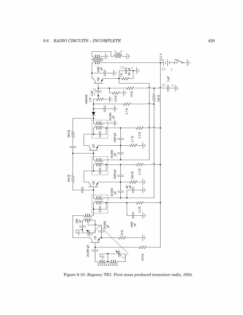
9.6. RADIO CIRCUITS – INCOMPLETE 429
10 K
2.2
K47
0 K20
,000
pF
Q1
268
pF
10,0
00 p
F 1000
pF
Q2
40 µF
1000
pF
560
Ω
50,0
00
pF
2.2
K
Q3
1000
pF
2.7
K
50,0
00
pF
2.2
K
560
Ω56
0 Ω
2.7
K
− +
2 µF
20,0
00
pF
1 K
100
K
Q4
40 µ
F
1 K
+ −
3.9
K 33 K
5 µF
+ −
+ −
22.5
V
1000
pF
volu
me
Figure 9.10: Regency TR1: First mass produced transistor radio, 1954.
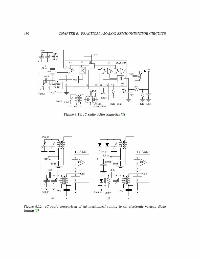
430 CHAPTER 9. PRACTICAL ANALOG SEMICONDUCTOR CIRCUITS
Vcc
Vcc
Vcc
AF
16 14
654
2
1
8 15 12
7
10311 13
9Osc.
RF IF
8.2K 25µF
47pF
47pF
5µF
3.3nF
39K
12K
100nF
100nF
100nF
330pF
320pF
370pF
1.5nF
TCA440
10nF
RF in
455 kHz Ceramic filter
Figure 9.11: IC radio, After Signetics [3]
Vcc
654
2
1
8
330pF
320pF
370pF
10nF
RF in
Vcc
654
2
1
8
330pF
270K
10nF
RF in
330nF
+Vtune
BB
113
BB113
Osc
RF RF
Osc
(a) (b)
TCA440 TCA440
Figure 9.12: IC radio comparison of (a) mechanical tuning to (b) electronic varicap diodetuning.[3]
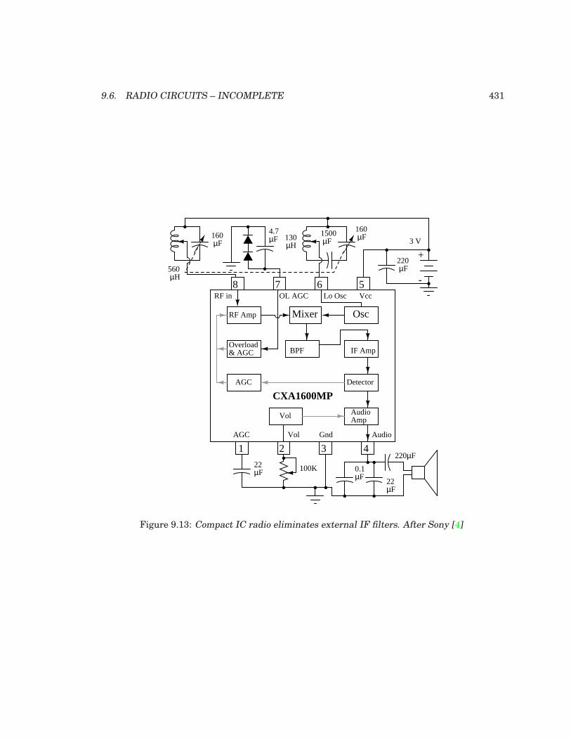
9.6. RADIO CIRCUITS – INCOMPLETE 431
1 2 3 4
5678VccLo OscRF in
RF Amp OscMixer
BPF IF Amp
Detector
AudioAmp
Overload& AGC
AGC
Vol
AGC Vol Gnd
OL AGC
Audio
22µF 100K
22µF
0.1µF
220µF
560 µH
160 µF130
µH
1500 µF
160 µF
4.7µF
220 µF
3 V
+
-
CXA1600MP
Figure 9.13: Compact IC radio eliminates external IF filters. After Sony [4]
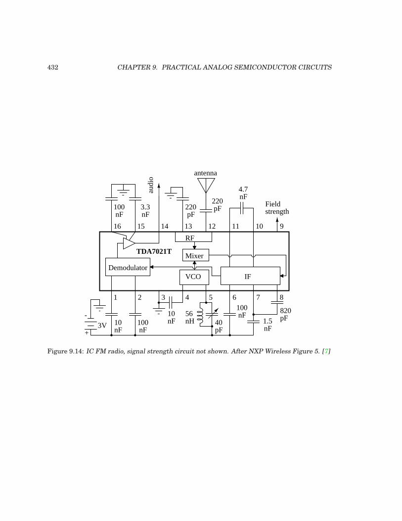
432 CHAPTER 9. PRACTICAL ANALOG SEMICONDUCTOR CIRCUITS
1 2 3 4 5 6 7 8
910111213141516
10nF
10nF100
nF
56nH
100 nF
1.5nF
820pF
40pF
220 pF
3.3nF
100 nF
220 pF
4.7nF
audi
o
antenna
+
-
TDA7021T
3V
IFVCO
RF
Mixer
Demodulator
Fieldstrength
Figure 9.14: IC FM radio, signal strength circuit not shown. After NXP Wireless Figure 5. [7]
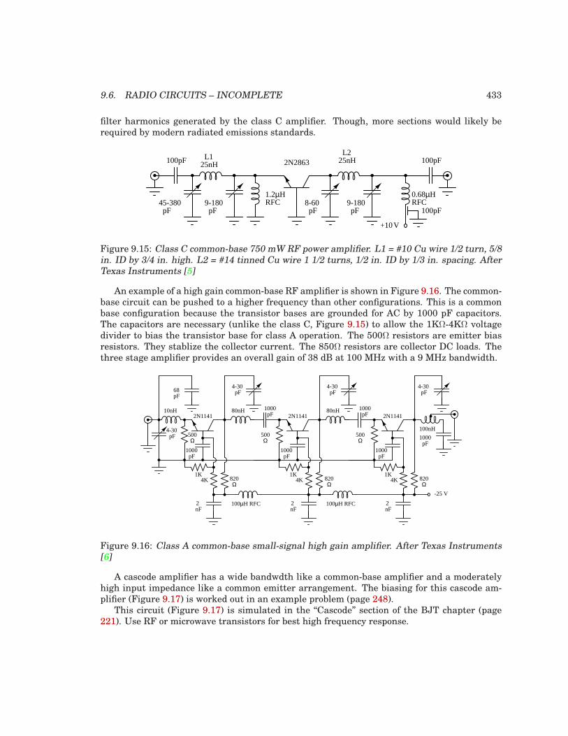
9.6. RADIO CIRCUITS – INCOMPLETE 433
filter harmonics generated by the class C amplifier. Though, more sections would likely berequired by modern radiated emissions standards.
+10V
100pF
100pF
0.68µHRFC
100pF
45-380 pF
9-180 pF
8-60 pF
9-180 pF
L125nH
L225nH
1.2µHRFC
2N2863
Figure 9.15: Class C common-base 750 mW RF power amplifier. L1 = #10 Cu wire 1/2 turn, 5/8in. ID by 3/4 in. high. L2 = #14 tinned Cu wire 1 1/2 turns, 1/2 in. ID by 1/3 in. spacing. AfterTexas Instruments [5]
An example of a high gain common-base RF amplifier is shown in Figure 9.16. The common-base circuit can be pushed to a higher frequency than other configurations. This is a commonbase configuration because the transistor bases are grounded for AC by 1000 pF capacitors.The capacitors are necessary (unlike the class C, Figure 9.15) to allow the 1KΩ-4KΩ voltagedivider to bias the transistor base for class A operation. The 500Ω resistors are emitter biasresistors. They stablize the collector current. The 850Ω resistors are collector DC loads. Thethree stage amplifier provides an overall gain of 38 dB at 100 MHz with a 9 MHz bandwidth.
1000 pF
4-30 pF
10nH2N1141
1K
500 Ω
80nH
68pF
1000 pF
4-30 pF
4K
2nF
100µH RFC
820 Ω
1000 pF
2N1141
1K
500 Ω
1000 pF
4K
2nF
100µH RFC
820 Ω
80nH
4-30 pF
1000 pF
2N1141
1K
500 Ω
4K
2nF
100nH
4-30 pF
820 Ω
-25 V
1000 pF
Figure 9.16: Class A common-base small-signal high gain amplifier. After Texas Instruments[6]
A cascode amplifier has a wide bandwdth like a common-base amplifier and a moderatelyhigh input impedance like a common emitter arrangement. The biasing for this cascode am-plifier (Figure 9.17) is worked out in an example problem (page 248).
This circuit (Figure 9.17) is simulated in the “Cascode” section of the BJT chapter (page221). Use RF or microwave transistors for best high frequency response.
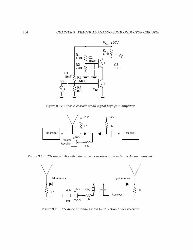
434 CHAPTER 9. PRACTICAL ANALOG SEMICONDUCTOR CIRCUITS
RL4.7k
Vi
Vo
VCC
Q1
Q2
VB2
R1150k
R2220k
R31Meg
R487k
20V
C110nF
C210nF
C310nF
Figure 9.17: Class A cascode small-signal high gain amplifier.
Transmitter Receiver
1 K 1 K
1 K
10 V 10 V
10 V
ReceiveTransmit
Figure 9.18: PIN diode T/R switch disconnects receiver from antenna during transmit.
Receiver1 K 1 K
1 K
5 V
left
right
-5 V
left antenna right antenna
RFC
Figure 9.19: PIN diode antenna switch for direction finder receiver.
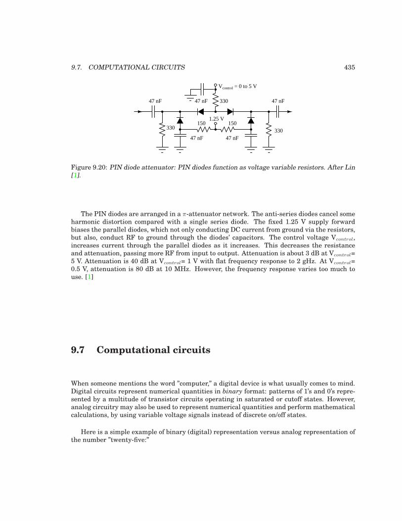
9.7. COMPUTATIONAL CIRCUITS 435
1.25 V
Vcontrol = 0 to 5 V
330330
330
150 150
47 nF 47 nF
47 nF47 nF 47 nF
Figure 9.20: PIN diode attenuator: PIN diodes function as voltage variable resistors. After Lin[1].
The PIN diodes are arranged in a π-attenuator network. The anti-series diodes cancel someharmonic distortion compared with a single series diode. The fixed 1.25 V supply forwardbiases the parallel diodes, which not only conducting DC current from ground via the resistors,but also, conduct RF to ground through the diodes’ capacitors. The control voltage Vcontrol,increases current through the parallel diodes as it increases. This decreases the resistanceand attenuation, passing more RF from input to output. Attenuation is about 3 dB at Vcontrol=5 V. Attenuation is 40 dB at Vcontrol= 1 V with flat frequency response to 2 gHz. At Vcontrol=0.5 V, attenuation is 80 dB at 10 MHz. However, the frequency response varies too much touse. [1]
9.7 Computational circuits
When someone mentions the word ”computer,” a digital device is what usually comes to mind.Digital circuits represent numerical quantities in binary format: patterns of 1’s and 0’s repre-sented by a multitude of transistor circuits operating in saturated or cutoff states. However,analog circuitry may also be used to represent numerical quantities and perform mathematicalcalculations, by using variable voltage signals instead of discrete on/off states.
Here is a simple example of binary (digital) representation versus analog representation ofthe number ”twenty-five:”
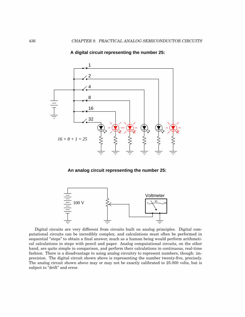
436 CHAPTER 9. PRACTICAL ANALOG SEMICONDUCTOR CIRCUITS
1
2
4
8
16
32
16 + 8 + 1 = 25
A digital circuit representing the number 25:
100 V 050
100
Voltmeter
An analog circuit representing the number 25:
Digital circuits are very different from circuits built on analog principles. Digital com-putational circuits can be incredibly complex, and calculations must often be performed insequential ”steps” to obtain a final answer, much as a human being would perform arithmeti-cal calculations in steps with pencil and paper. Analog computational circuits, on the otherhand, are quite simple in comparison, and perform their calculations in continuous, real-timefashion. There is a disadvantage to using analog circuitry to represent numbers, though: im-precision. The digital circuit shown above is representing the number twenty-five, precisely.The analog circuit shown above may or may not be exactly calibrated to 25.000 volts, but issubject to ”drift” and error.
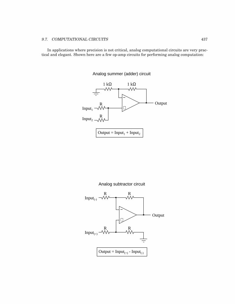
9.7. COMPUTATIONAL CIRCUITS 437
In applications where precision is not critical, analog computational circuits are very prac-tical and elegant. Shown here are a few op-amp circuits for performing analog computation:
−
+
1 kΩ
R
R
Input1
Input2
Output
Analog summer (adder) circuit
Output = Input1 + Input2
1 kΩ
−
+
R R
R RInput(+)
Input(-)
Output
Analog subtractor circuit
Output = Input(+) - Input(-)
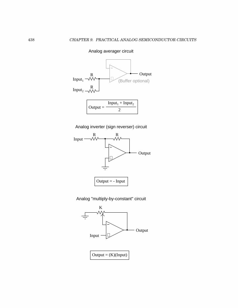
438 CHAPTER 9. PRACTICAL ANALOG SEMICONDUCTOR CIRCUITS
R
R
Input1
Input2
Output
Analog averager circuit
Output = Input1 + Input2
2
−
+ (Buffer optional)
Output−
+
Analog inverter (sign reverser) circuit
RRInput
Output = - Input
Output−
+ Input
K
Output = (K)(Input)
Analog "multiply-by-constant" circuit
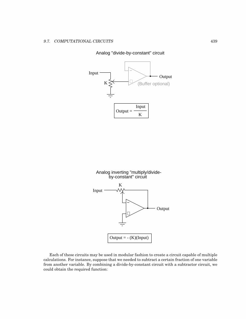
9.7. COMPUTATIONAL CIRCUITS 439
Output
Output =
−
+ (Buffer optional)
Input
K
Input
K
Analog "divide-by-constant" circuit
Output−
+
Input
Output = - (K)(Input)
K
Analog inverting "multiply/divide-by-constant" circuit
Each of these circuits may be used in modular fashion to create a circuit capable of multiplecalculations. For instance, suppose that we needed to subtract a certain fraction of one variablefrom another variable. By combining a divide-by-constant circuit with a subtractor circuit, wecould obtain the required function:
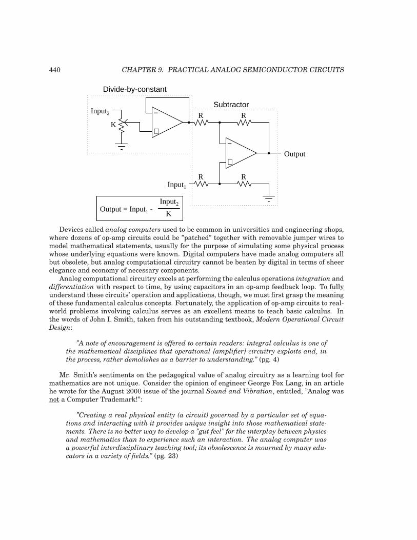
440 CHAPTER 9. PRACTICAL ANALOG SEMICONDUCTOR CIRCUITS
−
+
R R
R R
Output
Divide-by-constant
K
−
+
Subtractor
Output = Input1 - Input2
K
Input1
Input2
Devices called analog computers used to be common in universities and engineering shops,where dozens of op-amp circuits could be ”patched” together with removable jumper wires tomodel mathematical statements, usually for the purpose of simulating some physical processwhose underlying equations were known. Digital computers have made analog computers allbut obsolete, but analog computational circuitry cannot be beaten by digital in terms of sheerelegance and economy of necessary components.
Analog computational circuitry excels at performing the calculus operations integration anddifferentiation with respect to time, by using capacitors in an op-amp feedback loop. To fullyunderstand these circuits’ operation and applications, though, we must first grasp the meaningof these fundamental calculus concepts. Fortunately, the application of op-amp circuits to real-world problems involving calculus serves as an excellent means to teach basic calculus. Inthe words of John I. Smith, taken from his outstanding textbook, Modern Operational Circuit
Design:
”A note of encouragement is offered to certain readers: integral calculus is one of
the mathematical disciplines that operational [amplifier] circuitry exploits and, in
the process, rather demolishes as a barrier to understanding.” (pg. 4)
Mr. Smith’s sentiments on the pedagogical value of analog circuitry as a learning tool formathematics are not unique. Consider the opinion of engineer George Fox Lang, in an articlehe wrote for the August 2000 issue of the journal Sound and Vibration, entitled, ”Analog wasnot a Computer Trademark!”:
”Creating a real physical entity (a circuit) governed by a particular set of equa-
tions and interacting with it provides unique insight into those mathematical state-
ments. There is no better way to develop a ”gut feel” for the interplay between physics
and mathematics than to experience such an interaction. The analog computer was
a powerful interdisciplinary teaching tool; its obsolescence is mourned by many edu-
cators in a variety of fields.” (pg. 23)
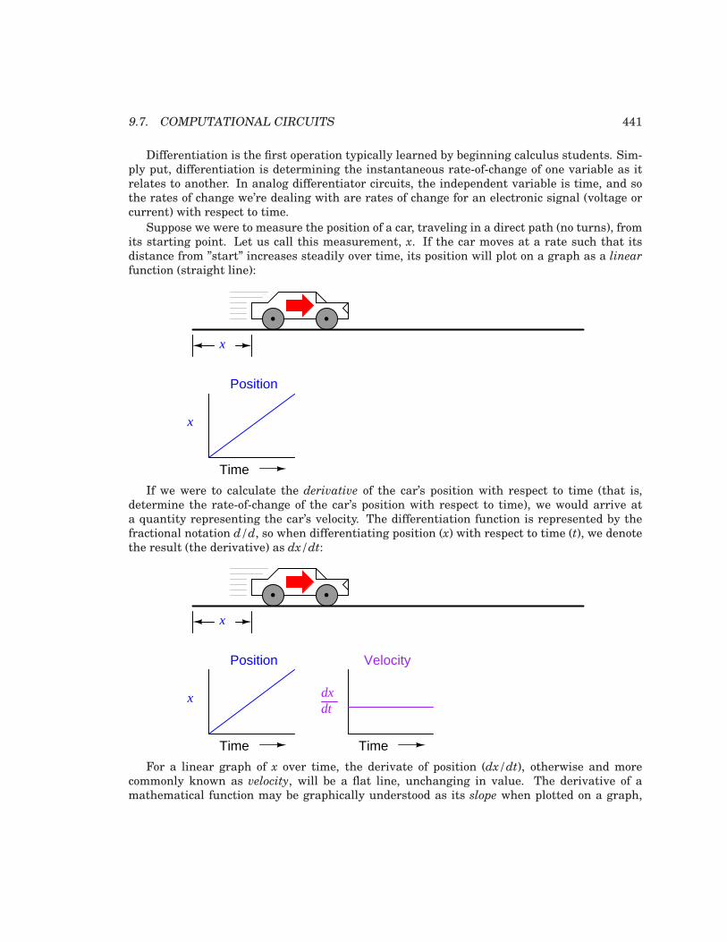
9.7. COMPUTATIONAL CIRCUITS 441
Differentiation is the first operation typically learned by beginning calculus students. Sim-ply put, differentiation is determining the instantaneous rate-of-change of one variable as itrelates to another. In analog differentiator circuits, the independent variable is time, and sothe rates of change we’re dealing with are rates of change for an electronic signal (voltage orcurrent) with respect to time.
Suppose we were to measure the position of a car, traveling in a direct path (no turns), fromits starting point. Let us call this measurement, x. If the car moves at a rate such that itsdistance from ”start” increases steadily over time, its position will plot on a graph as a linear
function (straight line):
x
x
Time
Position
If we were to calculate the derivative of the car’s position with respect to time (that is,determine the rate-of-change of the car’s position with respect to time), we would arrive ata quantity representing the car’s velocity. The differentiation function is represented by thefractional notation d/d, so when differentiating position (x) with respect to time (t), we denotethe result (the derivative) as dx/dt:
x
x
Time
Position
Time
dxdt
Velocity
For a linear graph of x over time, the derivate of position (dx/dt), otherwise and morecommonly known as velocity, will be a flat line, unchanging in value. The derivative of amathematical function may be graphically understood as its slope when plotted on a graph,
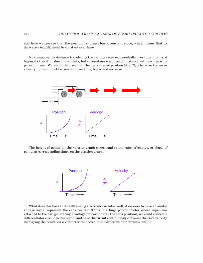
442 CHAPTER 9. PRACTICAL ANALOG SEMICONDUCTOR CIRCUITS
and here we can see that the position (x) graph has a constant slope, which means that itsderivative (dx/dt) must be constant over time.
Now, suppose the distance traveled by the car increased exponentially over time: that is, itbegan its travel in slow movements, but covered more additional distance with each passingperiod in time. We would then see that the derivative of position (dx/dt), otherwise known asvelocity (v), would not be constant over time, but would increase:
x
x
Time
Position
Time
dxdt
Velocity
The height of points on the velocity graph correspond to the rates-of-change, or slope, ofpoints at corresponding times on the position graph:
x
Time
Position
Time
dxdt
Velocity
What does this have to do with analog electronic circuits? Well, if we were to have an analogvoltage signal represent the car’s position (think of a huge potentiometer whose wiper wasattached to the car, generating a voltage proportional to the car’s position), we could connect adifferentiator circuit to this signal and have the circuit continuously calculate the car’s velocity,displaying the result via a voltmeter connected to the differentiator circuit’s output:
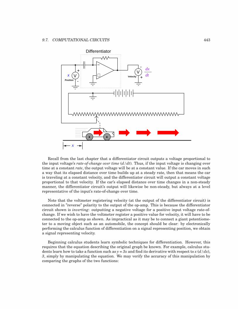
9.7. COMPUTATIONAL CIRCUITS 443
x
x
−
++
V-
+V
- dx
dt
Differentiator
Position
Velocity
Recall from the last chapter that a differentiator circuit outputs a voltage proportional tothe input voltage’s rate-of-change over time (d/dt). Thus, if the input voltage is changing overtime at a constant rate, the output voltage will be at a constant value. If the car moves in sucha way that its elapsed distance over time builds up at a steady rate, then that means the caris traveling at a constant velocity, and the differentiator circuit will output a constant voltageproportional to that velocity. If the car’s elapsed distance over time changes in a non-steadymanner, the differentiator circuit’s output will likewise be non-steady, but always at a levelrepresentative of the input’s rate-of-change over time.
Note that the voltmeter registering velocity (at the output of the differentiator circuit) isconnected in ”reverse” polarity to the output of the op-amp. This is because the differentiatorcircuit shown is inverting: outputting a negative voltage for a positive input voltage rate-of-change. If we wish to have the voltmeter register a positive value for velocity, it will have to beconnected to the op-amp as shown. As impractical as it may be to connect a giant potentiome-ter to a moving object such as an automobile, the concept should be clear: by electronicallyperforming the calculus function of differentiation on a signal representing position, we obtaina signal representing velocity.
Beginning calculus students learn symbolic techniques for differentiation. However, thisrequires that the equation describing the original graph be known. For example, calculus stu-dents learn how to take a function such as y = 3x and find its derivative with respect to x (d/dx),3, simply by manipulating the equation. We may verify the accuracy of this manipulation bycomparing the graphs of the two functions:
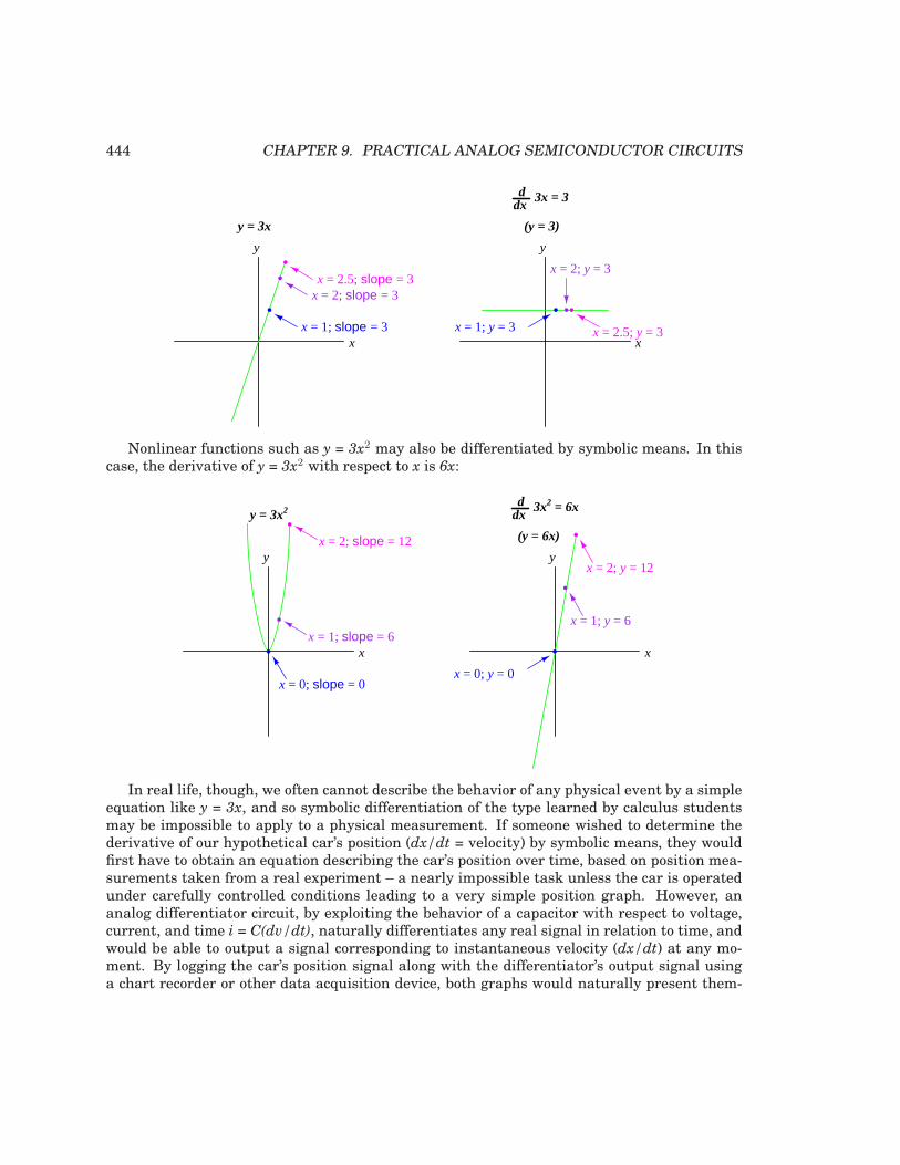
444 CHAPTER 9. PRACTICAL ANALOG SEMICONDUCTOR CIRCUITS
y
x
y
xx = 1; slope = 3
x = 2; slope = 3x = 2.5; slope = 3
y = 3x
x = 1; y = 3
x = 2; y = 3
x = 2.5; y = 3
dx3x = 3
(y = 3)
d
Nonlinear functions such as y = 3x2 may also be differentiated by symbolic means. In thiscase, the derivative of y = 3x2 with respect to x is 6x:
y
x
y
x
dxy = 3x2
x = 0; slope = 0
x = 1; slope = 6
3x2 = 6x
(y = 6x)x = 2; slope = 12
x = 0; y = 0
x = 1; y = 6
x = 2; y = 12
d
In real life, though, we often cannot describe the behavior of any physical event by a simpleequation like y = 3x, and so symbolic differentiation of the type learned by calculus studentsmay be impossible to apply to a physical measurement. If someone wished to determine thederivative of our hypothetical car’s position (dx/dt = velocity) by symbolic means, they wouldfirst have to obtain an equation describing the car’s position over time, based on position mea-surements taken from a real experiment – a nearly impossible task unless the car is operatedunder carefully controlled conditions leading to a very simple position graph. However, ananalog differentiator circuit, by exploiting the behavior of a capacitor with respect to voltage,current, and time i = C(dv/dt), naturally differentiates any real signal in relation to time, andwould be able to output a signal corresponding to instantaneous velocity (dx/dt) at any mo-ment. By logging the car’s position signal along with the differentiator’s output signal usinga chart recorder or other data acquisition device, both graphs would naturally present them-
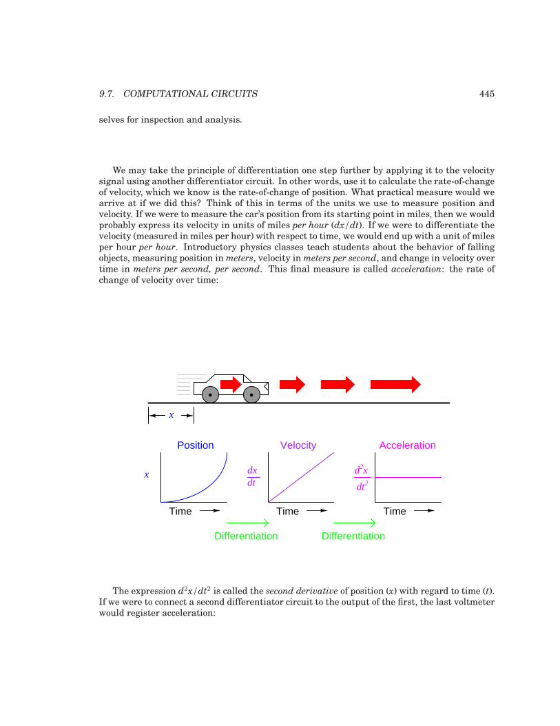
9.7. COMPUTATIONAL CIRCUITS 445
selves for inspection and analysis.
We may take the principle of differentiation one step further by applying it to the velocitysignal using another differentiator circuit. In other words, use it to calculate the rate-of-changeof velocity, which we know is the rate-of-change of position. What practical measure would wearrive at if we did this? Think of this in terms of the units we use to measure position andvelocity. If we were to measure the car’s position from its starting point in miles, then we wouldprobably express its velocity in units of miles per hour (dx/dt). If we were to differentiate thevelocity (measured in miles per hour) with respect to time, we would end up with a unit of milesper hour per hour. Introductory physics classes teach students about the behavior of fallingobjects, measuring position inmeters, velocity inmeters per second, and change in velocity overtime in meters per second, per second. This final measure is called acceleration: the rate ofchange of velocity over time:
x
x
Time
Position
Time
dxdt
Velocity
Time
Acceleration
d2x
dt2
Differentiation Differentiation
The expression d2x/dt2 is called the second derivative of position (x) with regard to time (t).If we were to connect a second differentiator circuit to the output of the first, the last voltmeterwould register acceleration:
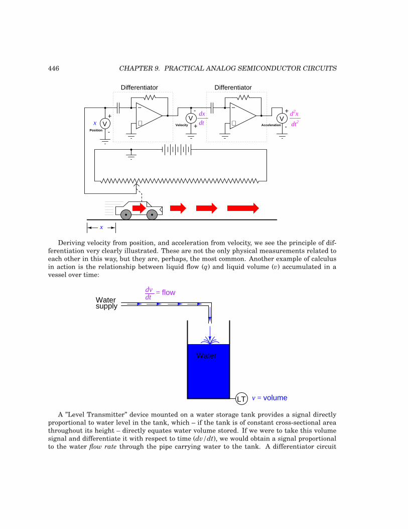
446 CHAPTER 9. PRACTICAL ANALOG SEMICONDUCTOR CIRCUITS
x
x
−
++
V-
+V
- dx
dt
Differentiator
Position
Velocity
−
+
Differentiator
+V
-Acceleration
d2x
dt2
Deriving velocity from position, and acceleration from velocity, we see the principle of dif-ferentiation very clearly illustrated. These are not the only physical measurements related toeach other in this way, but they are, perhaps, the most common. Another example of calculusin action is the relationship between liquid flow (q) and liquid volume (v) accumulated in avessel over time:
LT
Water
v = volume
dvdt
= flowWatersupply
A ”Level Transmitter” device mounted on a water storage tank provides a signal directlyproportional to water level in the tank, which – if the tank is of constant cross-sectional areathroughout its height – directly equates water volume stored. If we were to take this volumesignal and differentiate it with respect to time (dv/dt), we would obtain a signal proportionalto the water flow rate through the pipe carrying water to the tank. A differentiator circuit
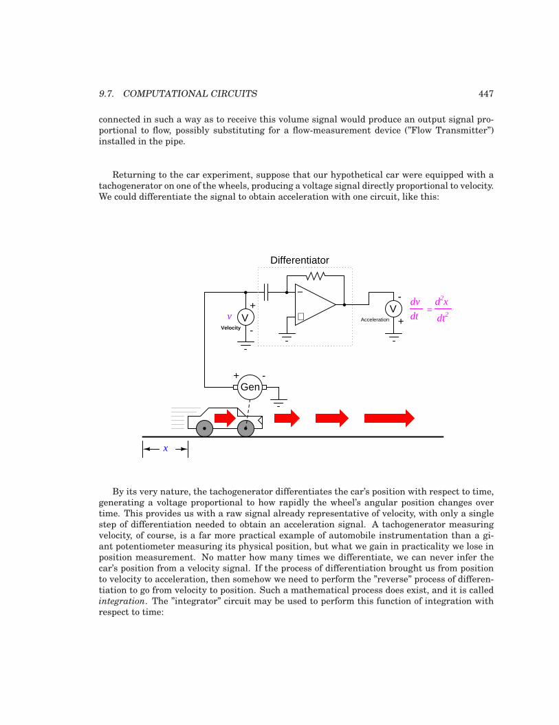
9.7. COMPUTATIONAL CIRCUITS 447
connected in such a way as to receive this volume signal would produce an output signal pro-portional to flow, possibly substituting for a flow-measurement device (”Flow Transmitter”)installed in the pipe.
Returning to the car experiment, suppose that our hypothetical car were equipped with atachogenerator on one of the wheels, producing a voltage signal directly proportional to velocity.We could differentiate the signal to obtain acceleration with one circuit, like this:
x
−
++
V-
+V
-
Differentiator
Velocity
v
d2x
dt2Acceleration
dv
dt=
Gen+ -
By its very nature, the tachogenerator differentiates the car’s position with respect to time,generating a voltage proportional to how rapidly the wheel’s angular position changes overtime. This provides us with a raw signal already representative of velocity, with only a singlestep of differentiation needed to obtain an acceleration signal. A tachogenerator measuringvelocity, of course, is a far more practical example of automobile instrumentation than a gi-ant potentiometer measuring its physical position, but what we gain in practicality we lose inposition measurement. No matter how many times we differentiate, we can never infer thecar’s position from a velocity signal. If the process of differentiation brought us from positionto velocity to acceleration, then somehow we need to perform the ”reverse” process of differen-tiation to go from velocity to position. Such a mathematical process does exist, and it is calledintegration. The ”integrator” circuit may be used to perform this function of integration withrespect to time:
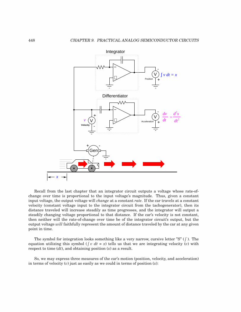
448 CHAPTER 9. PRACTICAL ANALOG SEMICONDUCTOR CIRCUITS
x
−
++
V-
+V
-
Differentiator
Velocity
v
d2x
dt2Acceleration
dv
dt=
Gen+ -
−
+
Integrator
+V
-
Position
∫ v dt = x
Recall from the last chapter that an integrator circuit outputs a voltage whose rate-of-change over time is proportional to the input voltage’s magnitude. Thus, given a constantinput voltage, the output voltage will change at a constant rate. If the car travels at a constantvelocity (constant voltage input to the integrator circuit from the tachogenerator), then itsdistance traveled will increase steadily as time progresses, and the integrator will output asteadily changing voltage proportional to that distance. If the car’s velocity is not constant,then neither will the rate-of-change over time be of the integrator circuit’s output, but theoutput voltage will faithfully represent the amount of distance traveled by the car at any givenpoint in time.
The symbol for integration looks something like a very narrow, cursive letter ”S” (∫). The
equation utilizing this symbol (∫v dt = x) tells us that we are integrating velocity (v) with
respect to time (dt), and obtaining position (x) as a result.
So, we may express three measures of the car’s motion (position, velocity, and acceleration)in terms of velocity (v) just as easily as we could in terms of position (x):
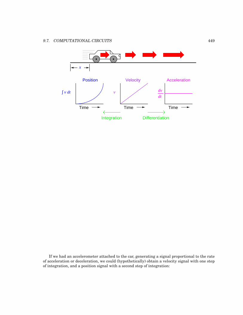
9.7. COMPUTATIONAL CIRCUITS 449
x
Time
Position
Time
Velocity
Time
Acceleration
DifferentiationIntegration
v dv
dt∫ v dt
If we had an accelerometer attached to the car, generating a signal proportional to the rateof acceleration or deceleration, we could (hypothetically) obtain a velocity signal with one stepof integration, and a position signal with a second step of integration:
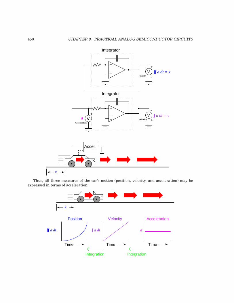
450 CHAPTER 9. PRACTICAL ANALOG SEMICONDUCTOR CIRCUITS
x
−
++
V-
+V
-
Velocity
Acceleration
−
+
Integrator
+V
-Position
Accel.
a
Integrator
∫ a dt = v
∫∫ a dt = x
Thus, all three measures of the car’s motion (position, velocity, and acceleration) may beexpressed in terms of acceleration:
x
Time
Position
Time
Velocity
Time
Acceleration
Integration Integration
a∫∫ a dt ∫ a dt
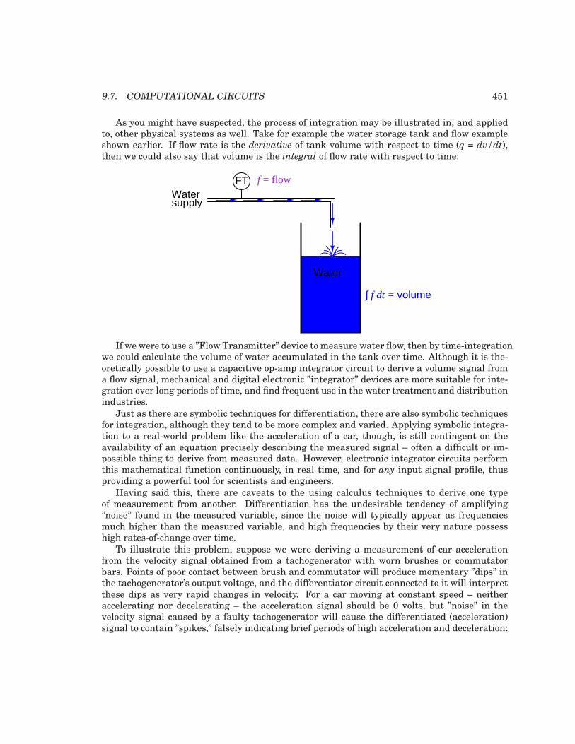
9.7. COMPUTATIONAL CIRCUITS 451
As you might have suspected, the process of integration may be illustrated in, and appliedto, other physical systems as well. Take for example the water storage tank and flow exampleshown earlier. If flow rate is the derivative of tank volume with respect to time (q = dv/dt),then we could also say that volume is the integral of flow rate with respect to time:
Water
Watersupply
FT f = flow
∫ f dt = volume
If we were to use a ”Flow Transmitter” device to measure water flow, then by time-integrationwe could calculate the volume of water accumulated in the tank over time. Although it is the-oretically possible to use a capacitive op-amp integrator circuit to derive a volume signal froma flow signal, mechanical and digital electronic ”integrator” devices are more suitable for inte-gration over long periods of time, and find frequent use in the water treatment and distributionindustries.
Just as there are symbolic techniques for differentiation, there are also symbolic techniquesfor integration, although they tend to be more complex and varied. Applying symbolic integra-tion to a real-world problem like the acceleration of a car, though, is still contingent on theavailability of an equation precisely describing the measured signal – often a difficult or im-possible thing to derive from measured data. However, electronic integrator circuits performthis mathematical function continuously, in real time, and for any input signal profile, thusproviding a powerful tool for scientists and engineers.
Having said this, there are caveats to the using calculus techniques to derive one typeof measurement from another. Differentiation has the undesirable tendency of amplifying”noise” found in the measured variable, since the noise will typically appear as frequenciesmuch higher than the measured variable, and high frequencies by their very nature possesshigh rates-of-change over time.
To illustrate this problem, suppose we were deriving a measurement of car accelerationfrom the velocity signal obtained from a tachogenerator with worn brushes or commutatorbars. Points of poor contact between brush and commutator will produce momentary ”dips” inthe tachogenerator’s output voltage, and the differentiator circuit connected to it will interpretthese dips as very rapid changes in velocity. For a car moving at constant speed – neitheraccelerating nor decelerating – the acceleration signal should be 0 volts, but ”noise” in thevelocity signal caused by a faulty tachogenerator will cause the differentiated (acceleration)signal to contain ”spikes,” falsely indicating brief periods of high acceleration and deceleration:
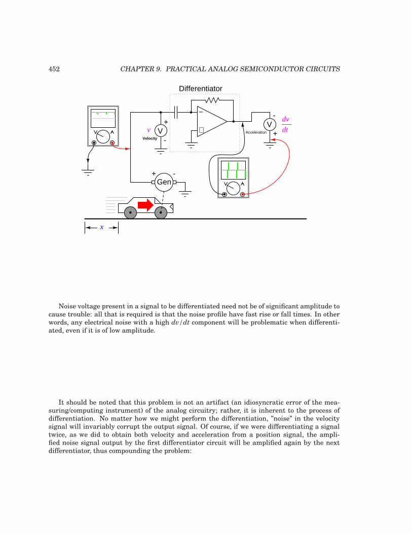
452 CHAPTER 9. PRACTICAL ANALOG SEMICONDUCTOR CIRCUITS
x
−
++
V-
+V
-
Differentiator
Velocity
v Acceleration
dv
dt
Gen+ -
Noise voltage present in a signal to be differentiated need not be of significant amplitude tocause trouble: all that is required is that the noise profile have fast rise or fall times. In otherwords, any electrical noise with a high dv/dt component will be problematic when differenti-ated, even if it is of low amplitude.
It should be noted that this problem is not an artifact (an idiosyncratic error of the mea-suring/computing instrument) of the analog circuitry; rather, it is inherent to the process ofdifferentiation. No matter how we might perform the differentiation, ”noise” in the velocitysignal will invariably corrupt the output signal. Of course, if we were differentiating a signaltwice, as we did to obtain both velocity and acceleration from a position signal, the ampli-fied noise signal output by the first differentiator circuit will be amplified again by the nextdifferentiator, thus compounding the problem:
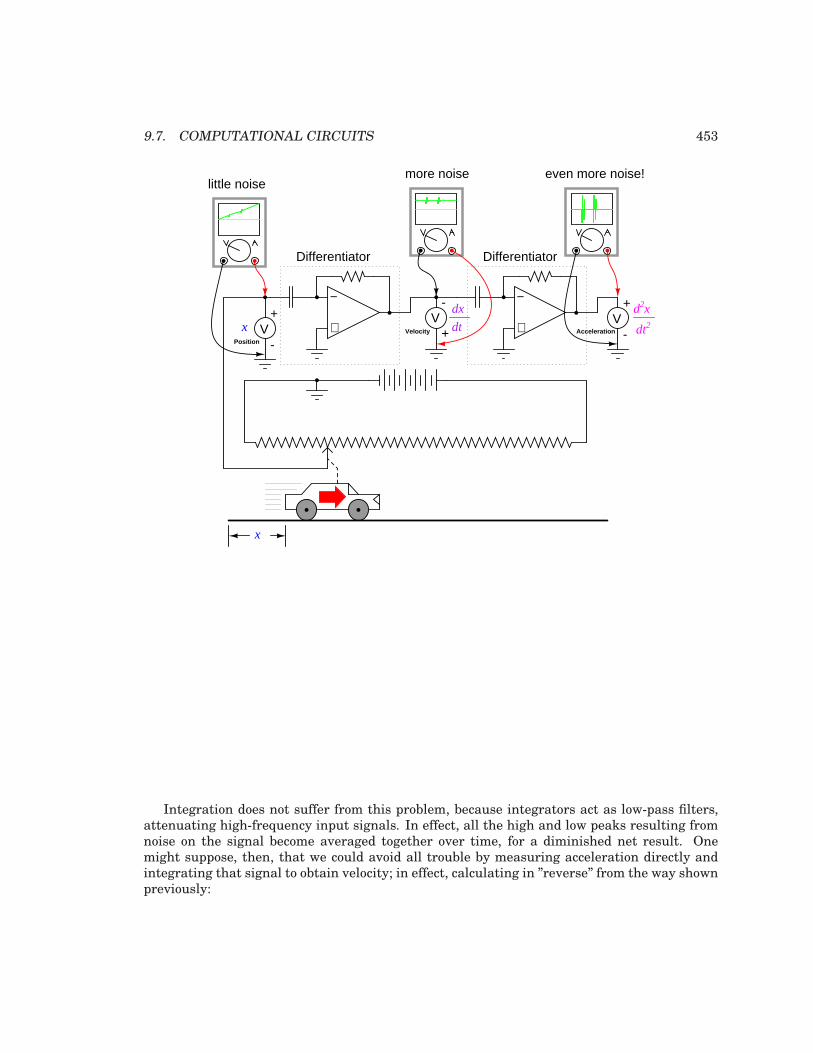
9.7. COMPUTATIONAL CIRCUITS 453
x
x
−
++
V-
+V
- dx
dt
Differentiator
Position
Velocity
−
+
Differentiator
+V
-Acceleration
d2x
dt2
little noisemore noise even more noise!
Integration does not suffer from this problem, because integrators act as low-pass filters,attenuating high-frequency input signals. In effect, all the high and low peaks resulting fromnoise on the signal become averaged together over time, for a diminished net result. Onemight suppose, then, that we could avoid all trouble by measuring acceleration directly andintegrating that signal to obtain velocity; in effect, calculating in ”reverse” from the way shownpreviously:
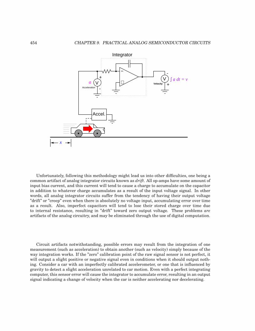
454 CHAPTER 9. PRACTICAL ANALOG SEMICONDUCTOR CIRCUITS
x
−
++
V-
+V
-
Velocity
Acceleration
Accel.
a
Integrator
∫ a dt = v
Unfortunately, following this methodology might lead us into other difficulties, one being acommon artifact of analog integrator circuits known as drift. All op-amps have some amount ofinput bias current, and this current will tend to cause a charge to accumulate on the capacitorin addition to whatever charge accumulates as a result of the input voltage signal. In otherwords, all analog integrator circuits suffer from the tendency of having their output voltage”drift” or ”creep” even when there is absolutely no voltage input, accumulating error over timeas a result. Also, imperfect capacitors will tend to lose their stored charge over time dueto internal resistance, resulting in ”drift” toward zero output voltage. These problems are
artifacts of the analog circuitry, and may be eliminated through the use of digital computation.
Circuit artifacts notwithstanding, possible errors may result from the integration of onemeasurement (such as acceleration) to obtain another (such as velocity) simply because of theway integration works. If the ”zero” calibration point of the raw signal sensor is not perfect, itwill output a slight positive or negative signal even in conditions when it should output noth-ing. Consider a car with an imperfectly calibrated accelerometer, or one that is influenced bygravity to detect a slight acceleration unrelated to car motion. Even with a perfect integratingcomputer, this sensor error will cause the integrator to accumulate error, resulting in an outputsignal indicating a change of velocity when the car is neither accelerating nor decelerating.
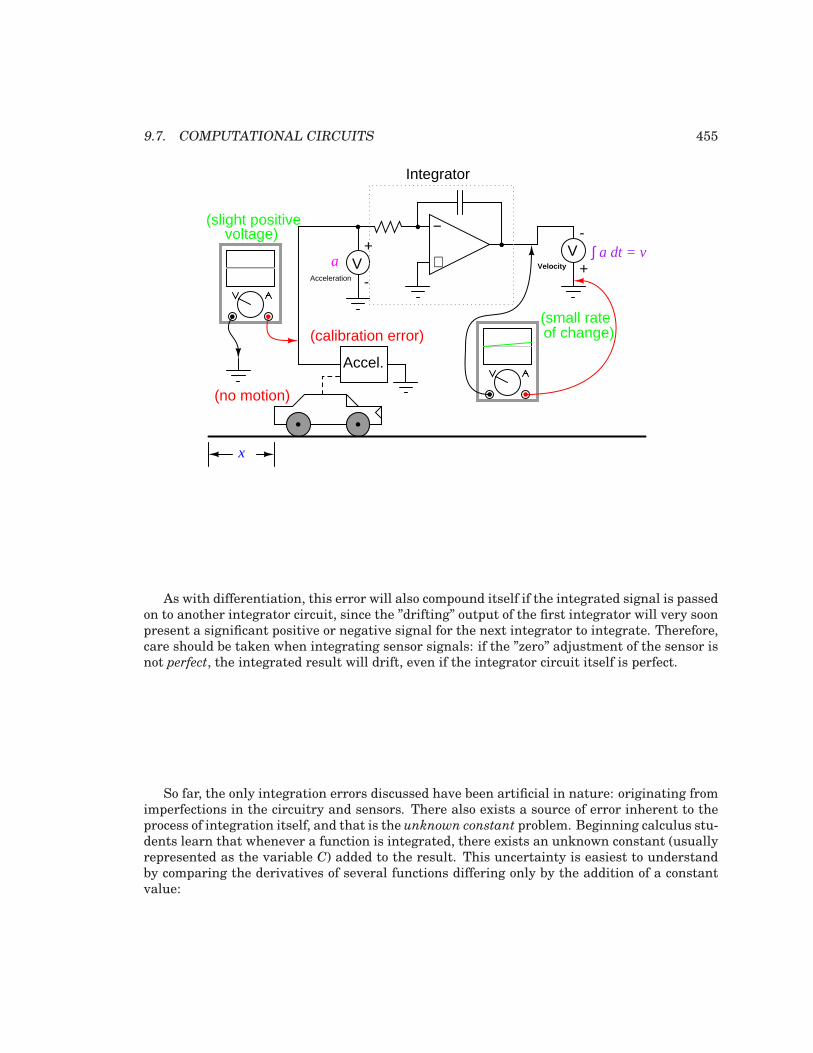
9.7. COMPUTATIONAL CIRCUITS 455
x
−
++
V-
+V
-
Velocity
Acceleration
Accel.
a
Integrator
∫ a dt = v
(no motion)
(slight positivevoltage)
(small rateof change)(calibration error)
As with differentiation, this error will also compound itself if the integrated signal is passedon to another integrator circuit, since the ”drifting” output of the first integrator will very soonpresent a significant positive or negative signal for the next integrator to integrate. Therefore,care should be taken when integrating sensor signals: if the ”zero” adjustment of the sensor isnot perfect, the integrated result will drift, even if the integrator circuit itself is perfect.
So far, the only integration errors discussed have been artificial in nature: originating fromimperfections in the circuitry and sensors. There also exists a source of error inherent to theprocess of integration itself, and that is the unknown constant problem. Beginning calculus stu-dents learn that whenever a function is integrated, there exists an unknown constant (usuallyrepresented as the variable C) added to the result. This uncertainty is easiest to understandby comparing the derivatives of several functions differing only by the addition of a constantvalue:
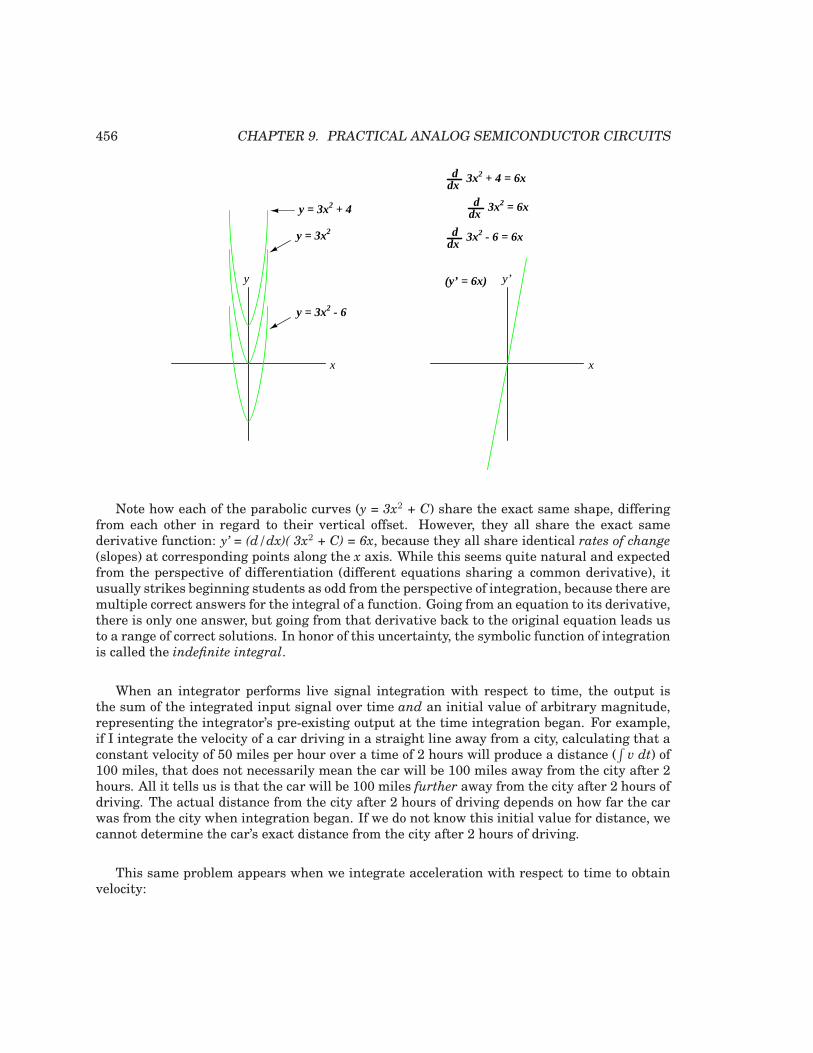
456 CHAPTER 9. PRACTICAL ANALOG SEMICONDUCTOR CIRCUITS
y
x x
dx
y = 3x2
3x2 = 6xd
(y’ = 6x) y’
y = 3x2 - 6
y = 3x2 + 4
3x2 + 4 = 6x
3x2 - 6 = 6x
dxd
dxd
Note how each of the parabolic curves (y = 3x2 + C) share the exact same shape, differingfrom each other in regard to their vertical offset. However, they all share the exact samederivative function: y’ = (d/dx)( 3x2 + C) = 6x, because they all share identical rates of change(slopes) at corresponding points along the x axis. While this seems quite natural and expectedfrom the perspective of differentiation (different equations sharing a common derivative), itusually strikes beginning students as odd from the perspective of integration, because there aremultiple correct answers for the integral of a function. Going from an equation to its derivative,there is only one answer, but going from that derivative back to the original equation leads usto a range of correct solutions. In honor of this uncertainty, the symbolic function of integrationis called the indefinite integral.
When an integrator performs live signal integration with respect to time, the output isthe sum of the integrated input signal over time and an initial value of arbitrary magnitude,representing the integrator’s pre-existing output at the time integration began. For example,if I integrate the velocity of a car driving in a straight line away from a city, calculating that aconstant velocity of 50 miles per hour over a time of 2 hours will produce a distance (
∫v dt) of
100 miles, that does not necessarily mean the car will be 100 miles away from the city after 2hours. All it tells us is that the car will be 100 miles further away from the city after 2 hours ofdriving. The actual distance from the city after 2 hours of driving depends on how far the carwas from the city when integration began. If we do not know this initial value for distance, wecannot determine the car’s exact distance from the city after 2 hours of driving.
This same problem appears when we integrate acceleration with respect to time to obtainvelocity:
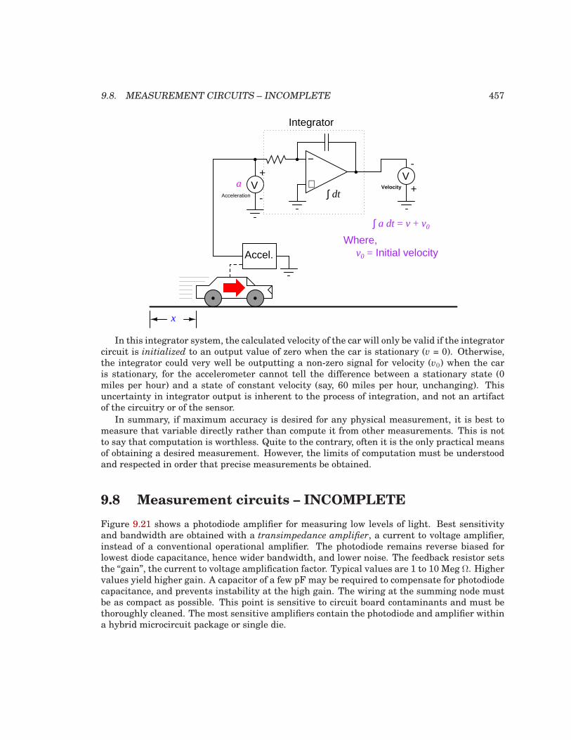
9.8. MEASUREMENT CIRCUITS – INCOMPLETE 457
x
−
++
V-
+V
-
Velocity
Acceleration
Accel.
a
Integrator
∫ dt
∫ a dt = v + v0
Where,v0 = Initial velocity
In this integrator system, the calculated velocity of the car will only be valid if the integratorcircuit is initialized to an output value of zero when the car is stationary (v = 0). Otherwise,the integrator could very well be outputting a non-zero signal for velocity (v0) when the caris stationary, for the accelerometer cannot tell the difference between a stationary state (0miles per hour) and a state of constant velocity (say, 60 miles per hour, unchanging). Thisuncertainty in integrator output is inherent to the process of integration, and not an artifactof the circuitry or of the sensor.
In summary, if maximum accuracy is desired for any physical measurement, it is best tomeasure that variable directly rather than compute it from other measurements. This is notto say that computation is worthless. Quite to the contrary, often it is the only practical meansof obtaining a desired measurement. However, the limits of computation must be understoodand respected in order that precise measurements be obtained.
9.8 Measurement circuits – INCOMPLETE
Figure 9.21 shows a photodiode amplifier for measuring low levels of light. Best sensitivityand bandwidth are obtained with a transimpedance amplifier, a current to voltage amplifier,instead of a conventional operational amplifier. The photodiode remains reverse biased forlowest diode capacitance, hence wider bandwidth, and lower noise. The feedback resistor setsthe “gain”, the current to voltage amplification factor. Typical values are 1 to 10 Meg Ω. Highervalues yield higher gain. A capacitor of a few pF may be required to compensate for photodiodecapacitance, and prevents instability at the high gain. The wiring at the summing node mustbe as compact as possible. This point is sensitive to circuit board contaminants and must bethoroughly cleaned. The most sensitive amplifiers contain the photodiode and amplifier withina hybrid microcircuit package or single die.
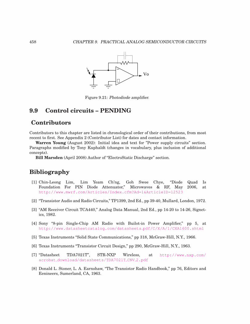
458 CHAPTER 9. PRACTICAL ANALOG SEMICONDUCTOR CIRCUITS
−
+Vo
Figure 9.21: Photodiode amplifier.
9.9 Control circuits – PENDING
Contributors
Contributors to this chapter are listed in chronological order of their contributions, from mostrecent to first. See Appendix 2 (Contributor List) for dates and contact information.
Warren Young (August 2002): Initial idea and text for ”Power supply circuits” section.Paragraphs modified by Tony Kuphaldt (changes in vocabulary, plus inclusion of additionalconcepts).
Bill Marsden (April 2008) Author of “ElectroStatic Discharge” section.
Bibliography
[1] Chin-Leong Lim, Lim Yeam Ch’ng, Goh Swee Chye, “Diode Quad IsFoundation For PIN Diode Attenuator,” Microwaves & RF, May 2006, athttp://www.mwrf.com/Articles/Index.cfm?Ad=1&Article ID=12523
[2] “Transistor Audio and Radio Circuits,” TP1399, 2nd Ed., pp 39-40, Mullard, London, 1972.
[3] “AM Receiver Circuit TCA440,” Analog Data Manual, 2nd Ed., pp 14-20 to 14-26, Signet-ics, 1982.
[4] Sony “8-pin Single-Chip AM Radio with Builot-in Power Amplifier,” pp 5, athttp://www.datasheetcatalog.com/datasheets pdf/C/X/A/1/CXA1600.shtml
[5] Texas Instruments “Solid State Communications,” pp 318, McGraw-Hill, N.Y., 1966.
[6] Texas Instruments “Transistor Circuit Design,” pp 290, McGraw-Hill, N.Y., 1963.
[7] “Datasheet TDA7021T”, STR-NXP Wireless, at http://www.nxp.com/acrobat download/datasheets/TDA7021T CNV2.pdf
[8] Donald L. Stoner, L. A. Earnshaw, “The Transistor Radio Handbook,” pp 76, Editors andEenineers, Sumerland, CA, 1963.

BIBLIOGRAPHY 459
[9] ,Charles Wenzel, “Crystal Radio Circuits,” at http://www.techlib.com/electronics/crystal.html .

460 CHAPTER 9. PRACTICAL ANALOG SEMICONDUCTOR CIRCUITS

Chapter 10
ACTIVE FILTERS
Contents
*** PENDING ***
461

462 CHAPTER 10. ACTIVE FILTERS
Chapter 11
DC MOTOR DRIVES
Contents
11.1 Pulse Width Modulation . . . . . . . . . . . . . . . . . . . . . . . . . . . . . . 463
*** INCOMPLETE ***
11.1 Pulse Width Modulation
Pulse Width Modulation (PWM) uses digital signals to control power applications, as well asbeing fairly easy to convert back to analog with a minimum of hardware.
Analog systems, such as linear power supplies, tend to generate a lot of heat since they arebasically variable resistors carrying a lot of current. Digital systems don’t generally generateas much heat. Almost all the heat generated by a switching device is during the transition(which is done quickly), while the device is neither on nor off, but in between. This is becausepower follows the following formula:
P = E I, or Watts = Voltage X Current
If either voltage or current is near zero then power will be near zero. PWM takes fulladvantage of this fact.
PWM can have many of the characteristics of an analog control system, in that the digitalsignal can be free wheeling. PWM does not have to capture data, although there are exceptionsto this with higher end controllers.
One of the parameters of any square wave is duty cycle. Most square waves are 50%, thisis the norm when discussing them, but they don’t have to be symmetrical. The ON time canbe varied completely between signal being off to being fully on, 0% to 100%, and all rangesbetween.
Shown below are examples of a 10%, 50%, and 90% duty cycle. While the frequency is thesame for each, this is not a requirement.
463
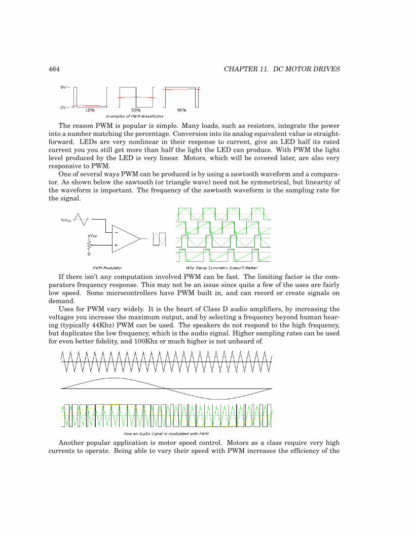
464 CHAPTER 11. DC MOTOR DRIVES
The reason PWM is popular is simple. Many loads, such as resistors, integrate the powerinto a number matching the percentage. Conversion into its analog equivalent value is straight-forward. LEDs are very nonlinear in their response to current, give an LED half its ratedcurrent you you still get more than half the light the LED can produce. With PWM the lightlevel produced by the LED is very linear. Motors, which will be covered later, are also veryresponsive to PWM.
One of several ways PWM can be produced is by using a sawtooth waveform and a compara-tor. As shown below the sawtooth (or triangle wave) need not be symmetrical, but linearity ofthe waveform is important. The frequency of the sawtooth waveform is the sampling rate forthe signal.
If there isn’t any computation involved PWM can be fast. The limiting factor is the com-parators frequency response. This may not be an issue since quite a few of the uses are fairlylow speed. Some microcontrollers have PWM built in, and can record or create signals ondemand.
Uses for PWM vary widely. It is the heart of Class D audio amplifiers, by increasing thevoltages you increase the maximum output, and by selecting a frequency beyond human hear-ing (typically 44Khz) PWM can be used. The speakers do not respond to the high frequency,but duplicates the low frequency, which is the audio signal. Higher sampling rates can be usedfor even better fidelity, and 100Khz or much higher is not unheard of.
Another popular application is motor speed control. Motors as a class require very highcurrents to operate. Being able to vary their speed with PWM increases the efficiency of the
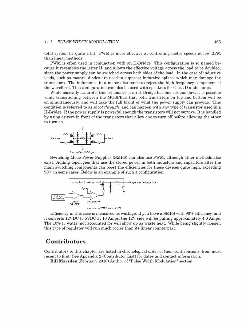
11.1. PULSE WIDTH MODULATION 465
total system by quite a bit. PWM is more effective at controlling motor speeds at low RPMthan linear methods.
PWM is often used in conjunction with an H-Bridge. This configuration is so named be-cause it resembles the letter H, and allows the effective voltage across the load to be doubled,since the power supply can be switched across both sides of the load. In the case of inductiveloads, such as motors, diodes are used to suppress inductive spikes, which may damage thetransistors. The inductance in a motor also tends to reject the high frequency component ofthe waveform. This configuration can also be used with speakers for Class D audio amps.
While basically accurate, this schematic of an H-Bridge has one serious flaw, it is possiblewhile transitioning between the MOSFETs that both transistors on top and bottom will beon simultaneously, and will take the full brunt of what the power supply can provide. Thiscondition is referred to as shoot through, and can happen with any type of transistor used in aH-Bridge. If the power supply is powerful enough the transistors will not survive. It is handledby using drivers in front of the transistors that allow one to turn off before allowing the otherto turn on.
Switching Mode Power Supplies (SMPS) can also use PWM, although other methods alsoexist. Adding topologies that use the stored power in both inductors and capacitors after themain switching components can boost the efficiencies for these devices quite high, exceeding90% in some cases. Below is an example of such a configuration.
Efficiency in this case is measured as wattage. If you have a SMPS with 90% efficiency, andit converts 12VDC to 5VDC at 10 Amps, the 12V side will be pulling approximately 4.6 Amps.The 10% (5 watts) not accounted for will show up as waste heat. While being slightly noisier,this type of regulator will run much cooler than its linear counterpart.
Contributors
Contributors to this chapter are listed in chronological order of their contributions, from mostrecent to first. See Appendix 2 (Contributor List) for dates and contact information.
Bill Marsden (February 2010) Author of “Pulse Width Modulation” section.

466 CHAPTER 11. DC MOTOR DRIVES
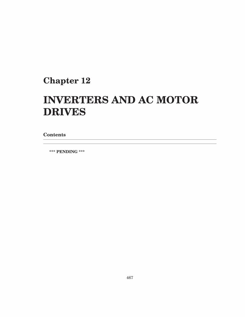
Chapter 12
INVERTERS AND AC MOTOR
DRIVES
Contents
*** PENDING ***
467

468 CHAPTER 12. INVERTERS AND AC MOTOR DRIVES
Chapter 13
ELECTRON TUBES
Contents
13.1 Introduction . . . . . . . . . . . . . . . . . . . . . . . . . . . . . . . . . . . . . . 469
13.2 Early tube history . . . . . . . . . . . . . . . . . . . . . . . . . . . . . . . . . . 470
13.3 The triode . . . . . . . . . . . . . . . . . . . . . . . . . . . . . . . . . . . . . . . 473
13.4 The tetrode . . . . . . . . . . . . . . . . . . . . . . . . . . . . . . . . . . . . . . . 475
13.5 Beam power tubes . . . . . . . . . . . . . . . . . . . . . . . . . . . . . . . . . . 476
13.6 The pentode . . . . . . . . . . . . . . . . . . . . . . . . . . . . . . . . . . . . . . 478
13.7 Combination tubes . . . . . . . . . . . . . . . . . . . . . . . . . . . . . . . . . . 478
13.8 Tube parameters . . . . . . . . . . . . . . . . . . . . . . . . . . . . . . . . . . . 481
13.9 Ionization (gas-filled) tubes . . . . . . . . . . . . . . . . . . . . . . . . . . . . 483
13.10Display tubes . . . . . . . . . . . . . . . . . . . . . . . . . . . . . . . . . . . . . 487
13.11Microwave tubes . . . . . . . . . . . . . . . . . . . . . . . . . . . . . . . . . . . 490
13.12Tubes versus Semiconductors . . . . . . . . . . . . . . . . . . . . . . . . . . . 493
13.1 Introduction
An often neglected area of study in modern electronics is that of tubes, more precisely known asvacuum tubes or electron tubes. Almost completely overshadowed by semiconductor, or ”solid-state” components in most modern applications, tube technology once dominated electroniccircuit design.
In fact, the historical transition from ”electric” to ”electronic” circuits really began withtubes, for it was with tubes that we entered into a whole new realm of circuit function: a way ofcontrolling the flow of electrons (current) in a circuit by means of another electric signal (in thecase of most tubes, the controlling signal is a small voltage). The semiconductor counterpartto the tube, of course, is the transistor. Transistors perform much the same function as tubes:controlling the flow of electrons in a circuit by means of another flow of electrons in the case ofthe bipolar transistor, and controlling the flow of electrons by means of a voltage in the case of
469
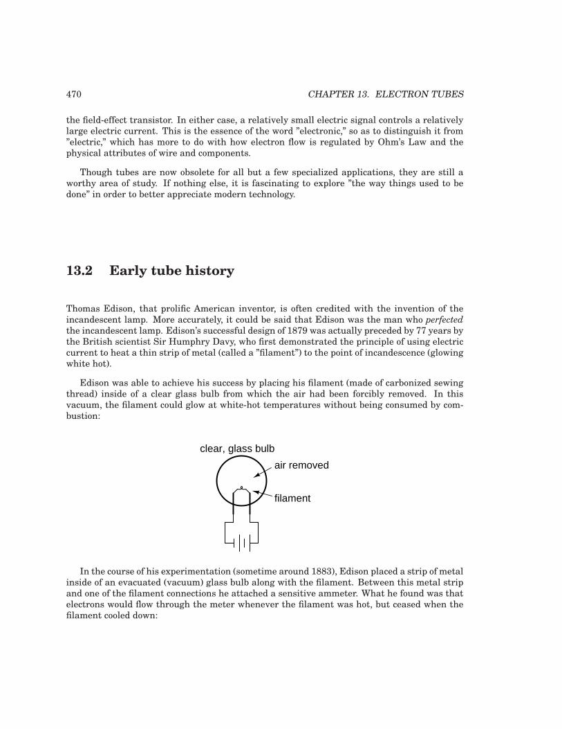
470 CHAPTER 13. ELECTRON TUBES
the field-effect transistor. In either case, a relatively small electric signal controls a relativelylarge electric current. This is the essence of the word ”electronic,” so as to distinguish it from”electric,” which has more to do with how electron flow is regulated by Ohm’s Law and thephysical attributes of wire and components.
Though tubes are now obsolete for all but a few specialized applications, they are still aworthy area of study. If nothing else, it is fascinating to explore ”the way things used to bedone” in order to better appreciate modern technology.
13.2 Early tube history
Thomas Edison, that prolific American inventor, is often credited with the invention of theincandescent lamp. More accurately, it could be said that Edison was the man who perfected
the incandescent lamp. Edison’s successful design of 1879 was actually preceded by 77 years bythe British scientist Sir Humphry Davy, who first demonstrated the principle of using electriccurrent to heat a thin strip of metal (called a ”filament”) to the point of incandescence (glowingwhite hot).
Edison was able to achieve his success by placing his filament (made of carbonized sewingthread) inside of a clear glass bulb from which the air had been forcibly removed. In thisvacuum, the filament could glow at white-hot temperatures without being consumed by com-bustion:
clear, glass bulb
air removed
filament
In the course of his experimentation (sometime around 1883), Edison placed a strip of metalinside of an evacuated (vacuum) glass bulb along with the filament. Between this metal stripand one of the filament connections he attached a sensitive ammeter. What he found was thatelectrons would flow through the meter whenever the filament was hot, but ceased when thefilament cooled down:
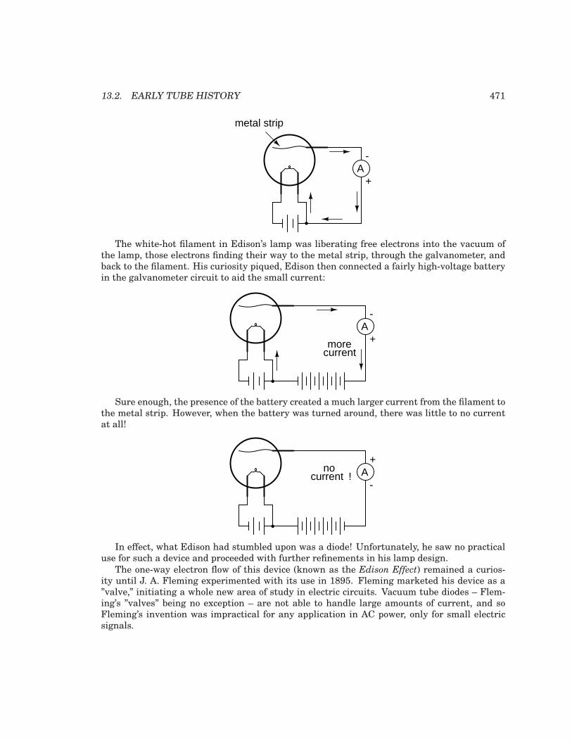
13.2. EARLY TUBE HISTORY 471
+A
-
metal strip
The white-hot filament in Edison’s lamp was liberating free electrons into the vacuum ofthe lamp, those electrons finding their way to the metal strip, through the galvanometer, andback to the filament. His curiosity piqued, Edison then connected a fairly high-voltage batteryin the galvanometer circuit to aid the small current:
+A
-
morecurrent
Sure enough, the presence of the battery created a much larger current from the filament tothe metal strip. However, when the battery was turned around, there was little to no currentat all!
+A
-current
no!
In effect, what Edison had stumbled upon was a diode! Unfortunately, he saw no practicaluse for such a device and proceeded with further refinements in his lamp design.
The one-way electron flow of this device (known as the Edison Effect) remained a curios-ity until J. A. Fleming experimented with its use in 1895. Fleming marketed his device as a”valve,” initiating a whole new area of study in electric circuits. Vacuum tube diodes – Flem-ing’s ”valves” being no exception – are not able to handle large amounts of current, and soFleming’s invention was impractical for any application in AC power, only for small electricsignals.
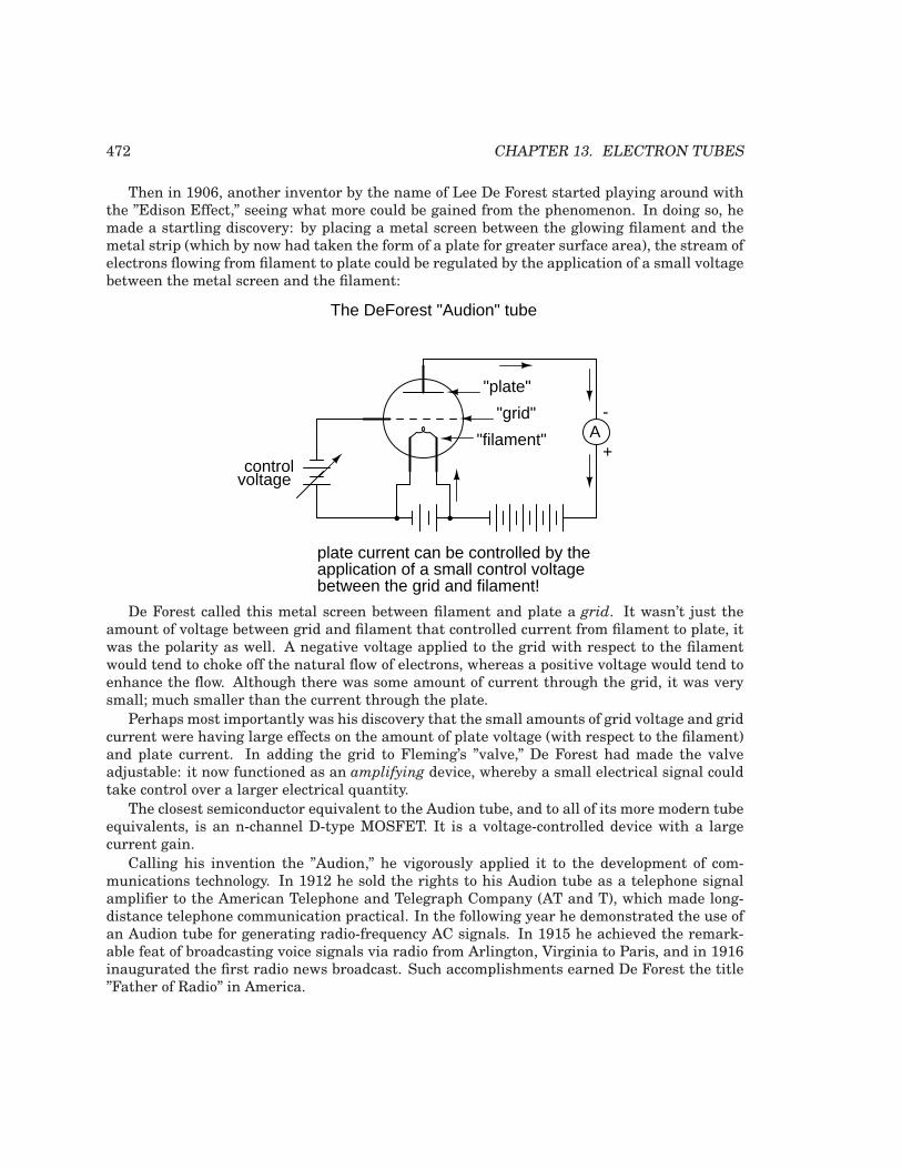
472 CHAPTER 13. ELECTRON TUBES
Then in 1906, another inventor by the name of Lee De Forest started playing around withthe ”Edison Effect,” seeing what more could be gained from the phenomenon. In doing so, hemade a startling discovery: by placing a metal screen between the glowing filament and themetal strip (which by now had taken the form of a plate for greater surface area), the stream ofelectrons flowing from filament to plate could be regulated by the application of a small voltagebetween the metal screen and the filament:
+A
-
controlvoltage
"plate"
"grid"
"filament"
plate current can be controlled by theapplication of a small control voltagebetween the grid and filament!
The DeForest "Audion" tube
De Forest called this metal screen between filament and plate a grid. It wasn’t just theamount of voltage between grid and filament that controlled current from filament to plate, itwas the polarity as well. A negative voltage applied to the grid with respect to the filamentwould tend to choke off the natural flow of electrons, whereas a positive voltage would tend toenhance the flow. Although there was some amount of current through the grid, it was verysmall; much smaller than the current through the plate.
Perhaps most importantly was his discovery that the small amounts of grid voltage and gridcurrent were having large effects on the amount of plate voltage (with respect to the filament)and plate current. In adding the grid to Fleming’s ”valve,” De Forest had made the valveadjustable: it now functioned as an amplifying device, whereby a small electrical signal couldtake control over a larger electrical quantity.
The closest semiconductor equivalent to the Audion tube, and to all of its more modern tubeequivalents, is an n-channel D-type MOSFET. It is a voltage-controlled device with a largecurrent gain.
Calling his invention the ”Audion,” he vigorously applied it to the development of com-munications technology. In 1912 he sold the rights to his Audion tube as a telephone signalamplifier to the American Telephone and Telegraph Company (AT and T), which made long-distance telephone communication practical. In the following year he demonstrated the use ofan Audion tube for generating radio-frequency AC signals. In 1915 he achieved the remark-able feat of broadcasting voice signals via radio from Arlington, Virginia to Paris, and in 1916inaugurated the first radio news broadcast. Such accomplishments earned De Forest the title”Father of Radio” in America.
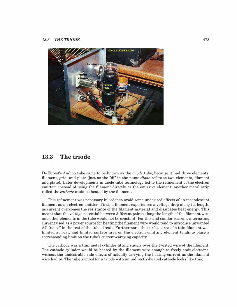
13.3. THE TRIODE 473
13.3 The triode
De Forest’s Audion tube came to be known as the triode tube, because it had three elements:filament, grid, and plate (just as the ”di” in the name diode refers to two elements, filamentand plate). Later developments in diode tube technology led to the refinement of the electronemitter: instead of using the filament directly as the emissive element, another metal stripcalled the cathode could be heated by the filament.
This refinement was necessary in order to avoid some undesired effects of an incandescentfilament as an electron emitter. First, a filament experiences a voltage drop along its length,as current overcomes the resistance of the filament material and dissipates heat energy. Thismeant that the voltage potential between different points along the length of the filament wireand other elements in the tube would not be constant. For this and similar reasons, alternatingcurrent used as a power source for heating the filament wire would tend to introduce unwantedAC ”noise” in the rest of the tube circuit. Furthermore, the surface area of a thin filament waslimited at best, and limited surface area on the electron emitting element tends to place acorresponding limit on the tube’s current-carrying capacity.
The cathode was a thin metal cylinder fitting snugly over the twisted wire of the filament.The cathode cylinder would be heated by the filament wire enough to freely emit electrons,without the undesirable side effects of actually carrying the heating current as the filamentwire had to. The tube symbol for a triode with an indirectly-heated cathode looks like this:
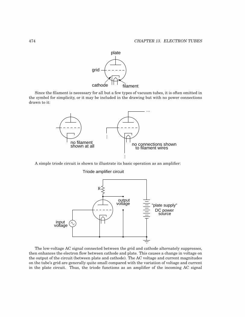
474 CHAPTER 13. ELECTRON TUBES
plate
grid
cathode filament
Since the filament is necessary for all but a few types of vacuum tubes, it is often omitted inthe symbol for simplicity, or it may be included in the drawing but with no power connectionsdrawn to it:
...
...
...
to filament wiresno connections shownno filament
shown at all
A simple triode circuit is shown to illustrate its basic operation as an amplifier:
R
voltageoutput
inputvoltage
DC powersource
"plate supply"
Triode amplifier circuit
The low-voltage AC signal connected between the grid and cathode alternately suppresses,then enhances the electron flow between cathode and plate. This causes a change in voltage onthe output of the circuit (between plate and cathode). The AC voltage and current magnitudeson the tube’s grid are generally quite small compared with the variation of voltage and currentin the plate circuit. Thus, the triode functions as an amplifier of the incoming AC signal
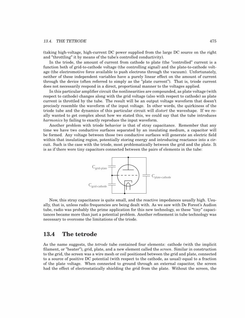
13.4. THE TETRODE 475
(taking high-voltage, high-current DC power supplied from the large DC source on the rightand ”throttling” it by means of the tube’s controlled conductivity).
In the triode, the amount of current from cathode to plate (the ”controlled” current is afunction both of grid-to-cathode voltage (the controlling signal) and the plate-to-cathode volt-age (the electromotive force available to push electrons through the vacuum). Unfortunately,neither of these independent variables have a purely linear effect on the amount of currentthrough the device (often referred to simply as the ”plate current”). That is, triode currentdoes not necessarily respond in a direct, proportional manner to the voltages applied.
In this particular amplifier circuit the nonlinearities are compounded, as plate voltage (withrespect to cathode) changes along with the grid voltage (also with respect to cathode) as platecurrent is throttled by the tube. The result will be an output voltage waveform that doesn’tprecisely resemble the waveform of the input voltage. In other words, the quirkiness of thetriode tube and the dynamics of this particular circuit will distort the waveshape. If we re-ally wanted to get complex about how we stated this, we could say that the tube introducesharmonics by failing to exactly reproduce the input waveform.
Another problem with triode behavior is that of stray capacitance. Remember that anytime we have two conductive surfaces separated by an insulating medium, a capacitor willbe formed. Any voltage between those two conductive surfaces will generate an electric fieldwithin that insulating region, potentially storing energy and introducing reactance into a cir-cuit. Such is the case with the triode, most problematically between the grid and the plate. Itis as if there were tiny capacitors connected between the pairs of elements in the tube:
Cgrid-plate
Cgrid-cathode
Cplate-cathode
Now, this stray capacitance is quite small, and the reactive impedances usually high. Usu-ally, that is, unless radio frequencies are being dealt with. As we saw with De Forest’s Audiontube, radio was probably the prime application for this new technology, so these ”tiny” capaci-tances became more than just a potential problem. Another refinement in tube technology wasnecessary to overcome the limitations of the triode.
13.4 The tetrode
As the name suggests, the tetrode tube contained four elements: cathode (with the implicitfilament, or ”heater”), grid, plate, and a new element called the screen. Similar in constructionto the grid, the screen was a wire mesh or coil positioned between the grid and plate, connectedto a source of positive DC potential (with respect to the cathode, as usual) equal to a fractionof the plate voltage. When connected to ground through an external capacitor, the screenhad the effect of electrostatically shielding the grid from the plate. Without the screen, the
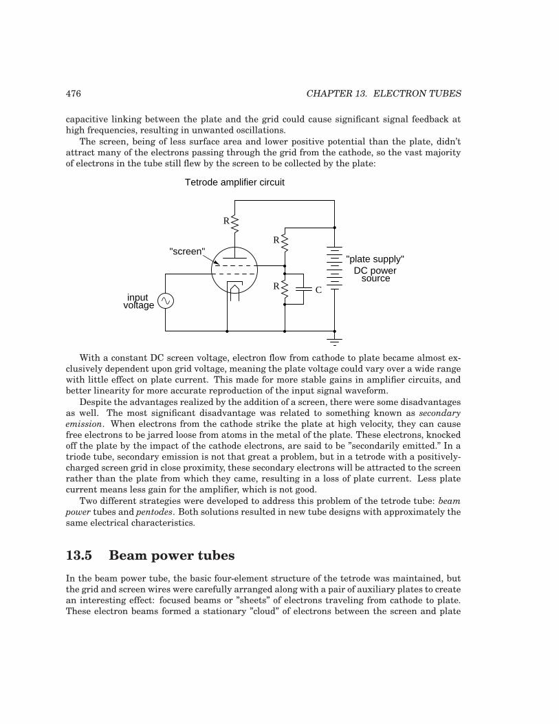
476 CHAPTER 13. ELECTRON TUBES
capacitive linking between the plate and the grid could cause significant signal feedback athigh frequencies, resulting in unwanted oscillations.
The screen, being of less surface area and lower positive potential than the plate, didn’tattract many of the electrons passing through the grid from the cathode, so the vast majorityof electrons in the tube still flew by the screen to be collected by the plate:
R
inputvoltage
DC powersource
"plate supply""screen"
R
R C
Tetrode amplifier circuit
With a constant DC screen voltage, electron flow from cathode to plate became almost ex-clusively dependent upon grid voltage, meaning the plate voltage could vary over a wide rangewith little effect on plate current. This made for more stable gains in amplifier circuits, andbetter linearity for more accurate reproduction of the input signal waveform.
Despite the advantages realized by the addition of a screen, there were some disadvantagesas well. The most significant disadvantage was related to something known as secondary
emission. When electrons from the cathode strike the plate at high velocity, they can causefree electrons to be jarred loose from atoms in the metal of the plate. These electrons, knockedoff the plate by the impact of the cathode electrons, are said to be ”secondarily emitted.” In atriode tube, secondary emission is not that great a problem, but in a tetrode with a positively-charged screen grid in close proximity, these secondary electrons will be attracted to the screenrather than the plate from which they came, resulting in a loss of plate current. Less platecurrent means less gain for the amplifier, which is not good.
Two different strategies were developed to address this problem of the tetrode tube: beampower tubes and pentodes. Both solutions resulted in new tube designs with approximately thesame electrical characteristics.
13.5 Beam power tubes
In the beam power tube, the basic four-element structure of the tetrode was maintained, butthe grid and screen wires were carefully arranged along with a pair of auxiliary plates to createan interesting effect: focused beams or ”sheets” of electrons traveling from cathode to plate.These electron beams formed a stationary ”cloud” of electrons between the screen and plate
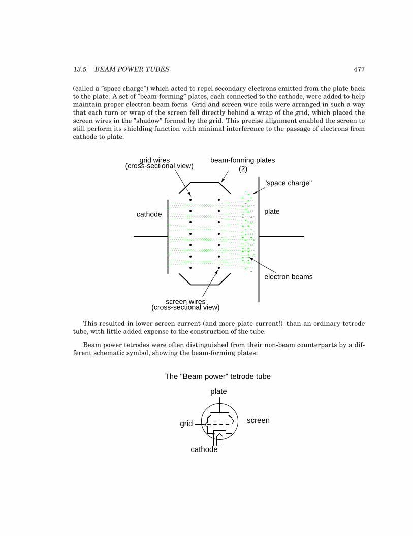
13.5. BEAM POWER TUBES 477
(called a ”space charge”) which acted to repel secondary electrons emitted from the plate backto the plate. A set of ”beam-forming” plates, each connected to the cathode, were added to helpmaintain proper electron beam focus. Grid and screen wire coils were arranged in such a waythat each turn or wrap of the screen fell directly behind a wrap of the grid, which placed thescreen wires in the ”shadow” formed by the grid. This precise alignment enabled the screen tostill perform its shielding function with minimal interference to the passage of electrons fromcathode to plate.
platecathode
grid wires(cross-sectional view)
(cross-sectional view)screen wires
beam-forming plates(2)
electron beams
-
-- --------- -
-------------- ---- -
- -
--
---
----
-
"space charge"
This resulted in lower screen current (and more plate current!) than an ordinary tetrodetube, with little added expense to the construction of the tube.
Beam power tetrodes were often distinguished from their non-beam counterparts by a dif-ferent schematic symbol, showing the beam-forming plates:
cathode
plate
screengrid
The "Beam power" tetrode tube
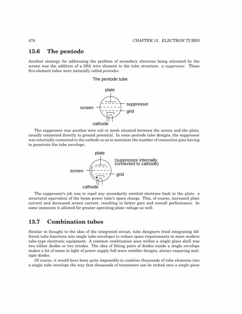
478 CHAPTER 13. ELECTRON TUBES
13.6 The pentode
Another strategy for addressing the problem of secondary electrons being attracted by thescreen was the addition of a fifth wire element to the tube structure: a suppressor. Thesefive-element tubes were naturally called pentodes.
cathode
grid
plate
screensuppressor
The pentode tube
The suppressor was another wire coil or mesh situated between the screen and the plate,usually connected directly to ground potential. In some pentode tube designs, the suppressorwas internally connected to the cathode so as to minimize the number of connection pins havingto penetrate the tube envelope:
cathode
grid
plate
screen
(suppressor internallyconnected to cathode)
The suppressor’s job was to repel any secondarily emitted electrons back to the plate: astructural equivalent of the beam power tube’s space charge. This, of course, increased platecurrent and decreased screen current, resulting in better gain and overall performance. Insome instances it allowed for greater operating plate voltage as well.
13.7 Combination tubes
Similar in thought to the idea of the integrated circuit, tube designers tried integrating dif-ferent tube functions into single tube envelopes to reduce space requirements in more moderntube-type electronic equipment. A common combination seen within a single glass shell wastwo either diodes or two triodes. The idea of fitting pairs of diodes inside a single envelopemakes a lot of sense in light of power supply full-wave rectifier designs, always requiring mul-tiple diodes.
Of course, it would have been quite impossible to combine thousands of tube elements intoa single tube envelope the way that thousands of transistors can be etched onto a single piece
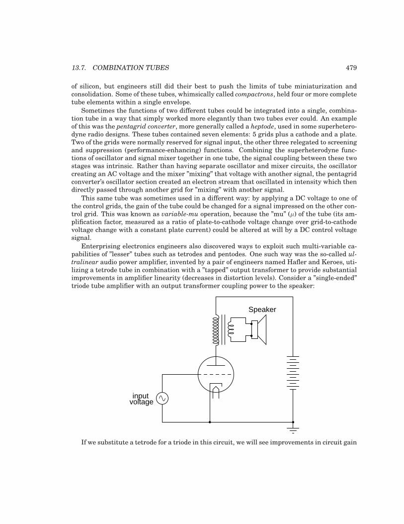
13.7. COMBINATION TUBES 479
of silicon, but engineers still did their best to push the limits of tube miniaturization andconsolidation. Some of these tubes, whimsically called compactrons, held four or more completetube elements within a single envelope.
Sometimes the functions of two different tubes could be integrated into a single, combina-tion tube in a way that simply worked more elegantly than two tubes ever could. An exampleof this was the pentagrid converter, more generally called a heptode, used in some superhetero-dyne radio designs. These tubes contained seven elements: 5 grids plus a cathode and a plate.Two of the grids were normally reserved for signal input, the other three relegated to screeningand suppression (performance-enhancing) functions. Combining the superheterodyne func-tions of oscillator and signal mixer together in one tube, the signal coupling between these twostages was intrinsic. Rather than having separate oscillator and mixer circuits, the oscillatorcreating an AC voltage and the mixer ”mixing” that voltage with another signal, the pentagridconverter’s oscillator section created an electron stream that oscillated in intensity which thendirectly passed through another grid for ”mixing” with another signal.
This same tube was sometimes used in a different way: by applying a DC voltage to one ofthe control grids, the gain of the tube could be changed for a signal impressed on the other con-trol grid. This was known as variable-mu operation, because the ”mu” (µ) of the tube (its am-plification factor, measured as a ratio of plate-to-cathode voltage change over grid-to-cathodevoltage change with a constant plate current) could be altered at will by a DC control voltagesignal.
Enterprising electronics engineers also discovered ways to exploit such multi-variable ca-pabilities of ”lesser” tubes such as tetrodes and pentodes. One such way was the so-called ul-
tralinear audio power amplifier, invented by a pair of engineers named Hafler and Keroes, uti-lizing a tetrode tube in combination with a ”tapped” output transformer to provide substantialimprovements in amplifier linearity (decreases in distortion levels). Consider a ”single-ended”triode tube amplifier with an output transformer coupling power to the speaker:
inputvoltage
Speaker
If we substitute a tetrode for a triode in this circuit, we will see improvements in circuit gain
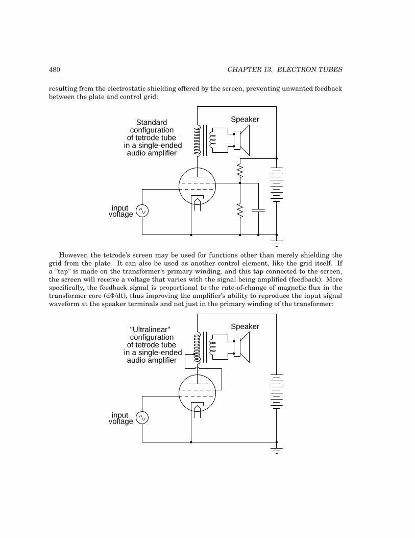
480 CHAPTER 13. ELECTRON TUBES
resulting from the electrostatic shielding offered by the screen, preventing unwanted feedbackbetween the plate and control grid:
inputvoltage
SpeakerStandard configuration
of tetrode tubein a single-endedaudio amplifier
However, the tetrode’s screen may be used for functions other than merely shielding thegrid from the plate. It can also be used as another control element, like the grid itself. Ifa ”tap” is made on the transformer’s primary winding, and this tap connected to the screen,the screen will receive a voltage that varies with the signal being amplified (feedback). Morespecifically, the feedback signal is proportional to the rate-of-change of magnetic flux in thetransformer core (dΦ/dt), thus improving the amplifier’s ability to reproduce the input signalwaveform at the speaker terminals and not just in the primary winding of the transformer:
inputvoltage
Speakerconfiguration
of tetrode tubein a single-endedaudio amplifier
"Ultralinear"
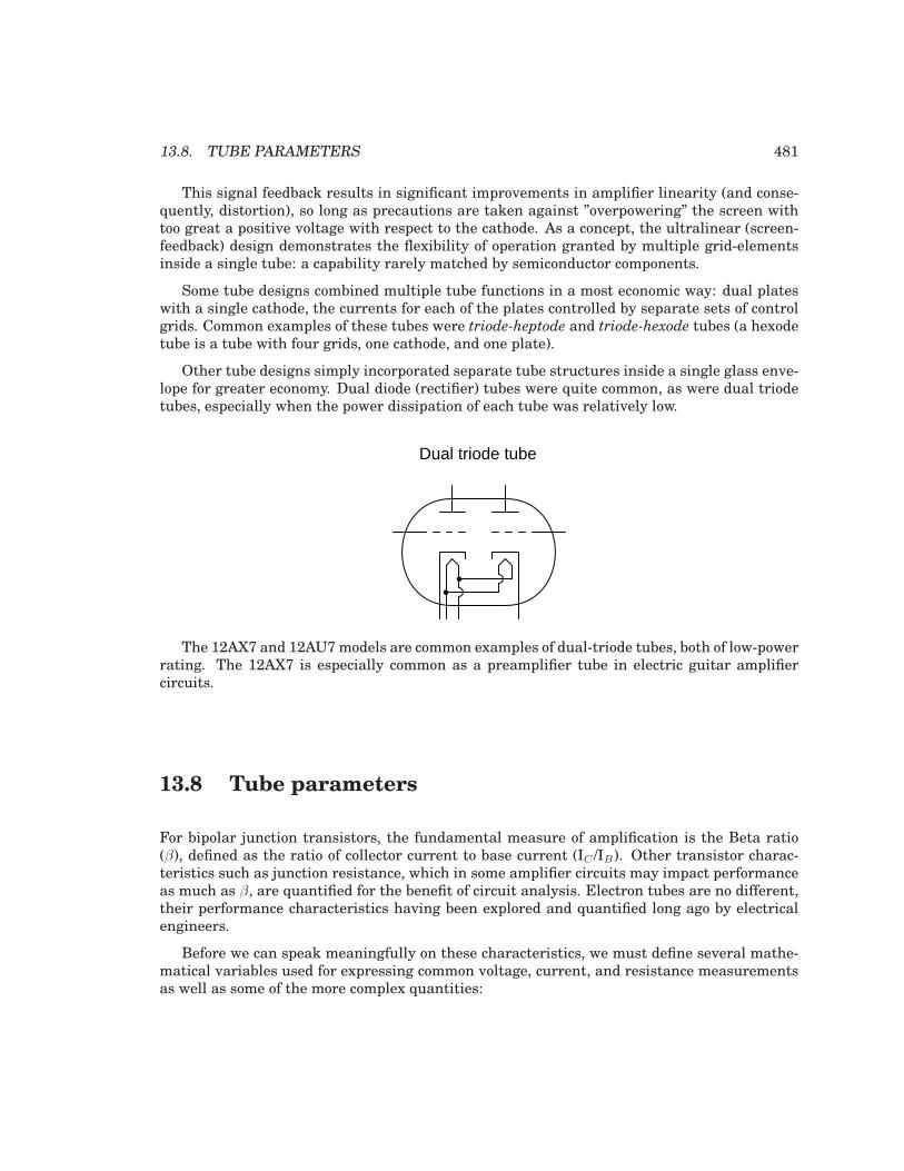
13.8. TUBE PARAMETERS 481
This signal feedback results in significant improvements in amplifier linearity (and conse-quently, distortion), so long as precautions are taken against ”overpowering” the screen withtoo great a positive voltage with respect to the cathode. As a concept, the ultralinear (screen-feedback) design demonstrates the flexibility of operation granted by multiple grid-elementsinside a single tube: a capability rarely matched by semiconductor components.
Some tube designs combined multiple tube functions in a most economic way: dual plateswith a single cathode, the currents for each of the plates controlled by separate sets of controlgrids. Common examples of these tubes were triode-heptode and triode-hexode tubes (a hexodetube is a tube with four grids, one cathode, and one plate).
Other tube designs simply incorporated separate tube structures inside a single glass enve-lope for greater economy. Dual diode (rectifier) tubes were quite common, as were dual triodetubes, especially when the power dissipation of each tube was relatively low.
Dual triode tube
The 12AX7 and 12AU7models are common examples of dual-triode tubes, both of low-powerrating. The 12AX7 is especially common as a preamplifier tube in electric guitar amplifiercircuits.
13.8 Tube parameters
For bipolar junction transistors, the fundamental measure of amplification is the Beta ratio(β), defined as the ratio of collector current to base current (IC /IB). Other transistor charac-teristics such as junction resistance, which in some amplifier circuits may impact performanceas much as β, are quantified for the benefit of circuit analysis. Electron tubes are no different,their performance characteristics having been explored and quantified long ago by electricalengineers.
Before we can speak meaningfully on these characteristics, we must define several mathe-matical variables used for expressing common voltage, current, and resistance measurementsas well as some of the more complex quantities:
482 CHAPTER 13. ELECTRON TUBES
µ = amplification factor, pronounced "mu"
gm = mutual conductance, in siemens(unitless)
Eg = grid-to-cathode voltage
Ip = plate current
Ep = plate-to-cathode voltage
Ik = cathode current
Es = input signal voltage
rp = dynamic plate resistance, in ohms
∆ = delta, the Greek symbol for change
The two most basic measures of an amplifying tube’s characteristics are its amplificationfactor (µ) and its mutual conductance (gm), also known as transconductance. Transconduc-tance is defined here just the same as it is for field-effect transistors, another category ofvoltage-controlled devices. Here are the two equations defining each of these performancecharacteristics:
µ =∆Ep
∆Eg
with constant Ip (plate current)
gm = ∆Ip
∆Eg
with constant Ep (plate voltage)
Another important, though more abstract, measure of tube performance is its plate resis-
tance. This is the measurement of plate voltage change over plate current change for a constantvalue of grid voltage. In other words, this is an expression of how much the tube acts like aresistor for any given amount of grid voltage, analogous to the operation of a JFET in its ohmicmode:
∆Eprp = ∆Ip
with constant Eg (grid voltage)
The astute reader will notice that plate resistance may be determined by dividing the am-plification factor by the transconductance:
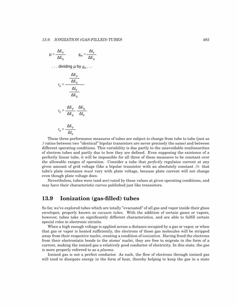
13.9. IONIZATION (GAS-FILLED) TUBES 483
∆Eprp = ∆Ip
µ = ∆Ep
∆Eg
gm = ∆Eg
∆Ip
. . . dividing µ by gm . . .
∆Ep
∆Eg
∆Ip
∆Eg
rp =
rp =∆Ep
∆Eg
∆Eg
∆Ip
These three performance measures of tubes are subject to change from tube to tube (just asβ ratios between two ”identical” bipolar transistors are never precisely the same) and betweendifferent operating conditions. This variability is due partly to the unavoidable nonlinearitiesof electron tubes and partly due to how they are defined. Even supposing the existence of aperfectly linear tube, it will be impossible for all three of these measures to be constant overthe allowable ranges of operation. Consider a tube that perfectly regulates current at anygiven amount of grid voltage (like a bipolar transistor with an absolutely constant β): thattube’s plate resistance must vary with plate voltage, because plate current will not changeeven though plate voltage does.
Nevertheless, tubes were (and are) rated by these values at given operating conditions, andmay have their characteristic curves published just like transistors.
13.9 Ionization (gas-filled) tubes
So far, we’ve explored tubes which are totally ”evacuated” of all gas and vapor inside their glassenvelopes, properly known as vacuum tubes. With the addition of certain gases or vapors,however, tubes take on significantly different characteristics, and are able to fulfill certainspecial roles in electronic circuits.
When a high enough voltage is applied across a distance occupied by a gas or vapor, or whenthat gas or vapor is heated sufficiently, the electrons of those gas molecules will be strippedaway from their respective nuclei, creating a condition of ionization. Having freed the electronsfrom their electrostatic bonds to the atoms’ nuclei, they are free to migrate in the form of acurrent, making the ionized gas a relatively good conductor of electricity. In this state, the gasis more properly referred to as a plasma.
Ionized gas is not a perfect conductor. As such, the flow of electrons through ionized gaswill tend to dissipate energy in the form of heat, thereby helping to keep the gas in a state
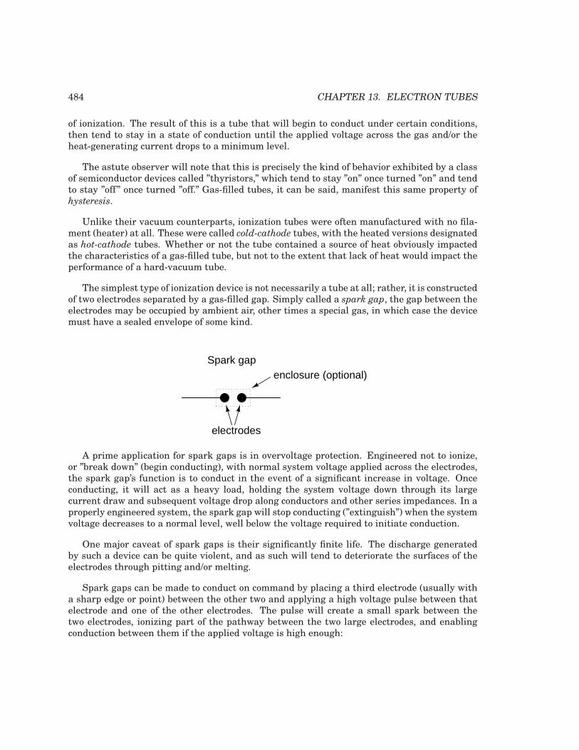
484 CHAPTER 13. ELECTRON TUBES
of ionization. The result of this is a tube that will begin to conduct under certain conditions,then tend to stay in a state of conduction until the applied voltage across the gas and/or theheat-generating current drops to a minimum level.
The astute observer will note that this is precisely the kind of behavior exhibited by a classof semiconductor devices called ”thyristors,” which tend to stay ”on” once turned ”on” and tendto stay ”off” once turned ”off.” Gas-filled tubes, it can be said, manifest this same property ofhysteresis.
Unlike their vacuum counterparts, ionization tubes were often manufactured with no fila-ment (heater) at all. These were called cold-cathode tubes, with the heated versions designatedas hot-cathode tubes. Whether or not the tube contained a source of heat obviously impactedthe characteristics of a gas-filled tube, but not to the extent that lack of heat would impact theperformance of a hard-vacuum tube.
The simplest type of ionization device is not necessarily a tube at all; rather, it is constructedof two electrodes separated by a gas-filled gap. Simply called a spark gap, the gap between theelectrodes may be occupied by ambient air, other times a special gas, in which case the devicemust have a sealed envelope of some kind.
electrodes
enclosure (optional)Spark gap
A prime application for spark gaps is in overvoltage protection. Engineered not to ionize,or ”break down” (begin conducting), with normal system voltage applied across the electrodes,the spark gap’s function is to conduct in the event of a significant increase in voltage. Onceconducting, it will act as a heavy load, holding the system voltage down through its largecurrent draw and subsequent voltage drop along conductors and other series impedances. In aproperly engineered system, the spark gap will stop conducting (”extinguish”) when the systemvoltage decreases to a normal level, well below the voltage required to initiate conduction.
One major caveat of spark gaps is their significantly finite life. The discharge generatedby such a device can be quite violent, and as such will tend to deteriorate the surfaces of theelectrodes through pitting and/or melting.
Spark gaps can be made to conduct on command by placing a third electrode (usually witha sharp edge or point) between the other two and applying a high voltage pulse between thatelectrode and one of the other electrodes. The pulse will create a small spark between thetwo electrodes, ionizing part of the pathway between the two large electrodes, and enablingconduction between them if the applied voltage is high enough:
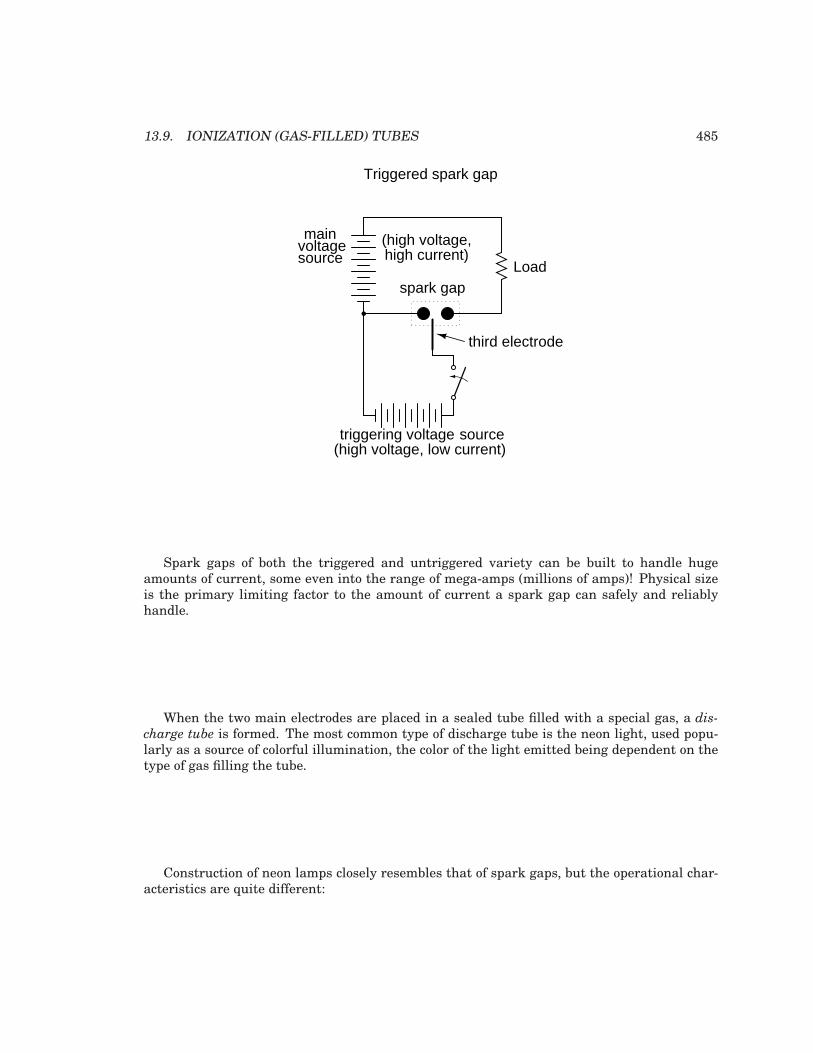
13.9. IONIZATION (GAS-FILLED) TUBES 485
third electrode
Load
triggering voltage
mainvoltagesource
source(high voltage, low current)
(high voltage,high current)
spark gap
Triggered spark gap
Spark gaps of both the triggered and untriggered variety can be built to handle hugeamounts of current, some even into the range of mega-amps (millions of amps)! Physical sizeis the primary limiting factor to the amount of current a spark gap can safely and reliablyhandle.
When the two main electrodes are placed in a sealed tube filled with a special gas, a dis-
charge tube is formed. The most common type of discharge tube is the neon light, used popu-larly as a source of colorful illumination, the color of the light emitted being dependent on thetype of gas filling the tube.
Construction of neon lamps closely resembles that of spark gaps, but the operational char-acteristics are quite different:
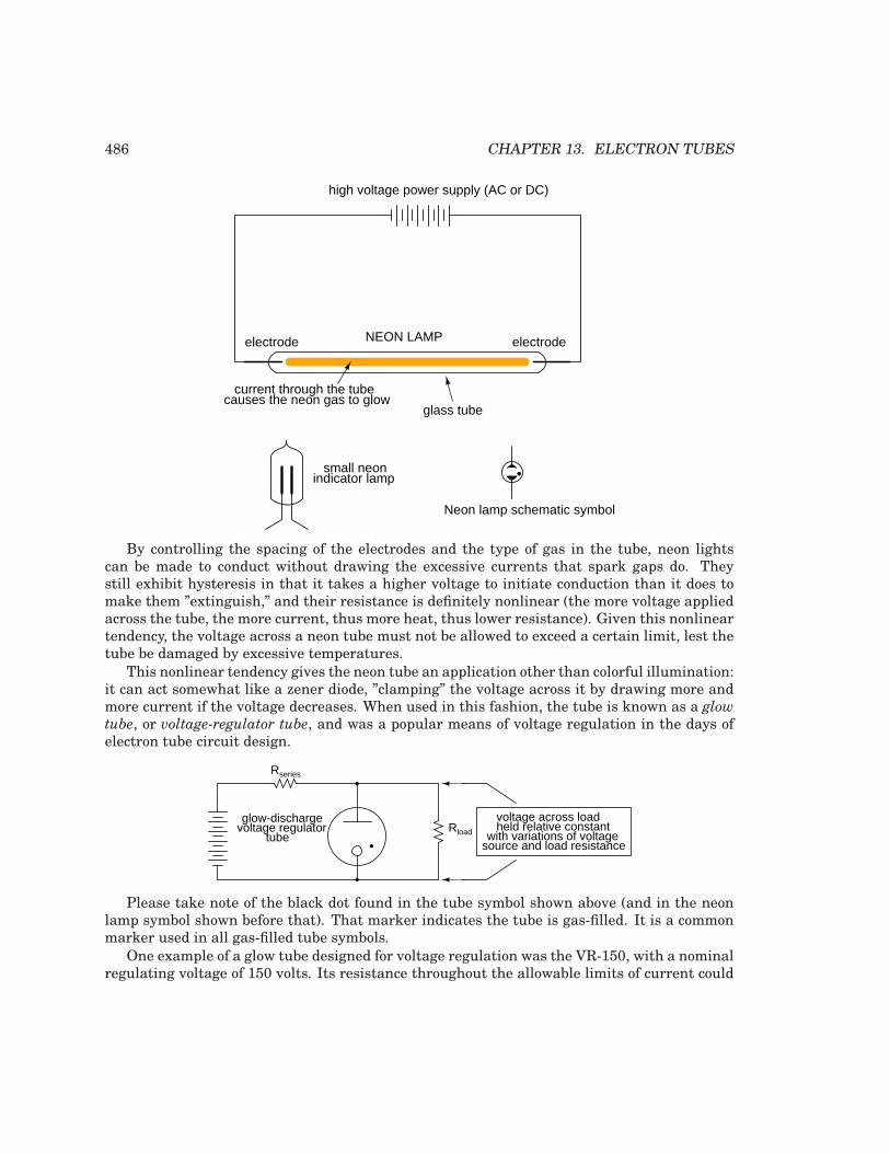
486 CHAPTER 13. ELECTRON TUBES
electrode electrode
glass tube
current through the tubecauses the neon gas to glow
NEON LAMP
high voltage power supply (AC or DC)
small neonindicator lamp
Neon lamp schematic symbol
By controlling the spacing of the electrodes and the type of gas in the tube, neon lightscan be made to conduct without drawing the excessive currents that spark gaps do. Theystill exhibit hysteresis in that it takes a higher voltage to initiate conduction than it does tomake them ”extinguish,” and their resistance is definitely nonlinear (the more voltage appliedacross the tube, the more current, thus more heat, thus lower resistance). Given this nonlineartendency, the voltage across a neon tube must not be allowed to exceed a certain limit, lest thetube be damaged by excessive temperatures.
This nonlinear tendency gives the neon tube an application other than colorful illumination:it can act somewhat like a zener diode, ”clamping” the voltage across it by drawing more andmore current if the voltage decreases. When used in this fashion, the tube is known as a glow
tube, or voltage-regulator tube, and was a popular means of voltage regulation in the days ofelectron tube circuit design.
Rload
Rseries
glow-dischargevoltage regulator
tube
voltage across loadheld relative constant
with variations of voltagesource and load resistance
Please take note of the black dot found in the tube symbol shown above (and in the neonlamp symbol shown before that). That marker indicates the tube is gas-filled. It is a commonmarker used in all gas-filled tube symbols.
One example of a glow tube designed for voltage regulation was the VR-150, with a nominalregulating voltage of 150 volts. Its resistance throughout the allowable limits of current could
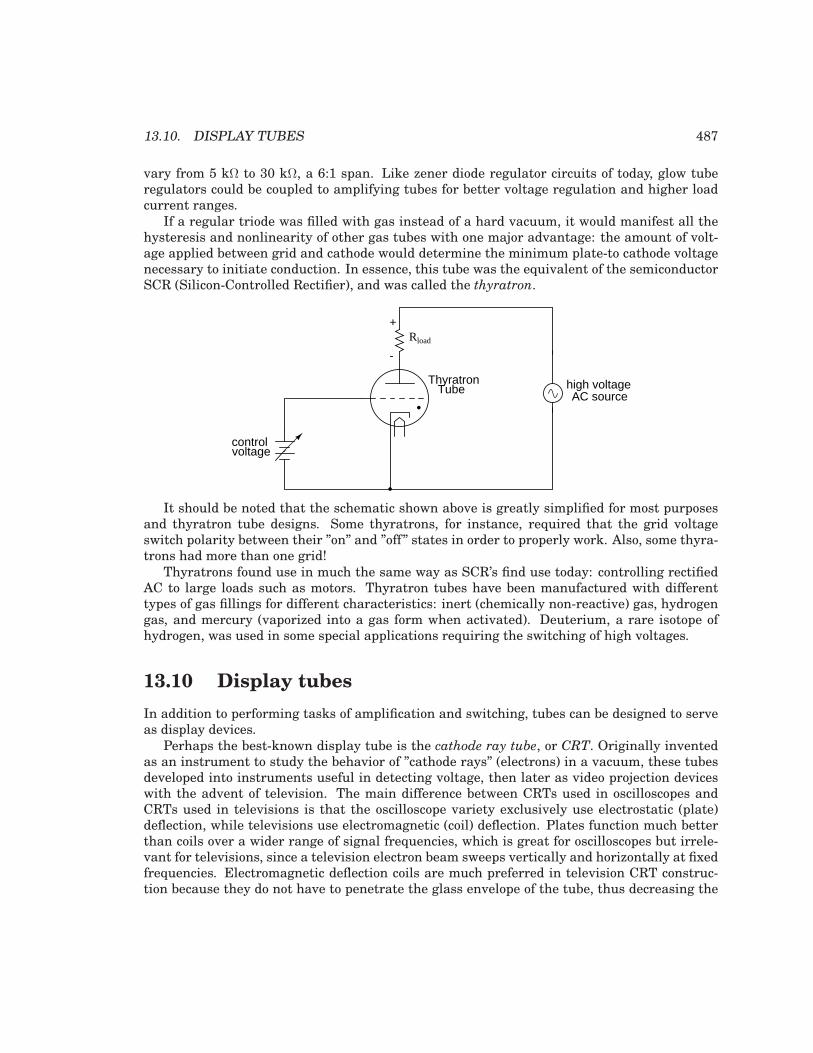
13.10. DISPLAY TUBES 487
vary from 5 kΩ to 30 kΩ, a 6:1 span. Like zener diode regulator circuits of today, glow tuberegulators could be coupled to amplifying tubes for better voltage regulation and higher loadcurrent ranges.
If a regular triode was filled with gas instead of a hard vacuum, it would manifest all thehysteresis and nonlinearity of other gas tubes with one major advantage: the amount of volt-age applied between grid and cathode would determine the minimum plate-to cathode voltagenecessary to initiate conduction. In essence, this tube was the equivalent of the semiconductorSCR (Silicon-Controlled Rectifier), and was called the thyratron.
Rload
controlvoltage
ThyratronTube high voltage
AC source
+
-
It should be noted that the schematic shown above is greatly simplified for most purposesand thyratron tube designs. Some thyratrons, for instance, required that the grid voltageswitch polarity between their ”on” and ”off” states in order to properly work. Also, some thyra-trons had more than one grid!
Thyratrons found use in much the same way as SCR’s find use today: controlling rectifiedAC to large loads such as motors. Thyratron tubes have been manufactured with differenttypes of gas fillings for different characteristics: inert (chemically non-reactive) gas, hydrogengas, and mercury (vaporized into a gas form when activated). Deuterium, a rare isotope ofhydrogen, was used in some special applications requiring the switching of high voltages.
13.10 Display tubes
In addition to performing tasks of amplification and switching, tubes can be designed to serveas display devices.
Perhaps the best-known display tube is the cathode ray tube, or CRT. Originally inventedas an instrument to study the behavior of ”cathode rays” (electrons) in a vacuum, these tubesdeveloped into instruments useful in detecting voltage, then later as video projection deviceswith the advent of television. The main difference between CRTs used in oscilloscopes andCRTs used in televisions is that the oscilloscope variety exclusively use electrostatic (plate)deflection, while televisions use electromagnetic (coil) deflection. Plates function much betterthan coils over a wider range of signal frequencies, which is great for oscilloscopes but irrele-vant for televisions, since a television electron beam sweeps vertically and horizontally at fixedfrequencies. Electromagnetic deflection coils are much preferred in television CRT construc-tion because they do not have to penetrate the glass envelope of the tube, thus decreasing the
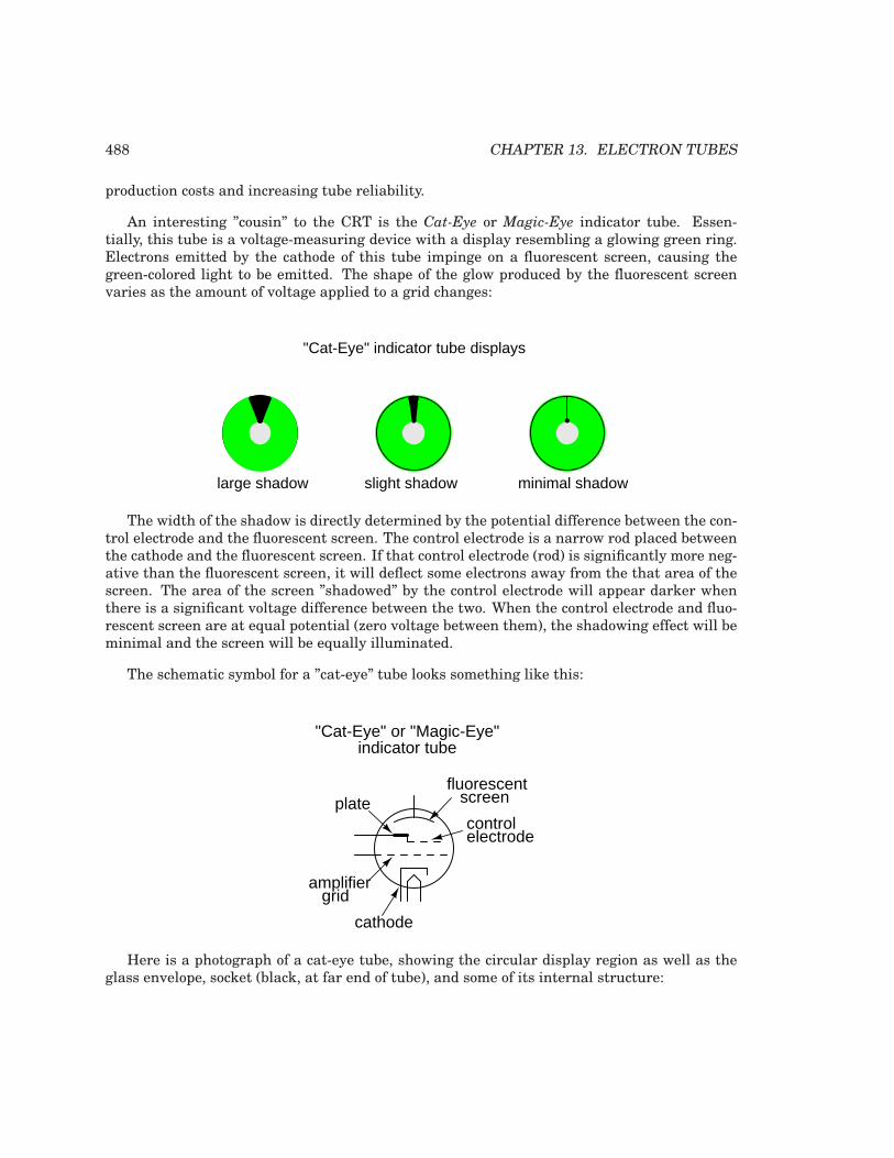
488 CHAPTER 13. ELECTRON TUBES
production costs and increasing tube reliability.
An interesting ”cousin” to the CRT is the Cat-Eye or Magic-Eye indicator tube. Essen-tially, this tube is a voltage-measuring device with a display resembling a glowing green ring.Electrons emitted by the cathode of this tube impinge on a fluorescent screen, causing thegreen-colored light to be emitted. The shape of the glow produced by the fluorescent screenvaries as the amount of voltage applied to a grid changes:
minimal shadowslight shadowlarge shadow
"Cat-Eye" indicator tube displays
The width of the shadow is directly determined by the potential difference between the con-trol electrode and the fluorescent screen. The control electrode is a narrow rod placed betweenthe cathode and the fluorescent screen. If that control electrode (rod) is significantly more neg-ative than the fluorescent screen, it will deflect some electrons away from the that area of thescreen. The area of the screen ”shadowed” by the control electrode will appear darker whenthere is a significant voltage difference between the two. When the control electrode and fluo-rescent screen are at equal potential (zero voltage between them), the shadowing effect will beminimal and the screen will be equally illuminated.
The schematic symbol for a ”cat-eye” tube looks something like this:
screenplatecontrol
amplifiergrid
cathode
electrode
fluorescent
"Cat-Eye" or "Magic-Eye"indicator tube
Here is a photograph of a cat-eye tube, showing the circular display region as well as theglass envelope, socket (black, at far end of tube), and some of its internal structure:
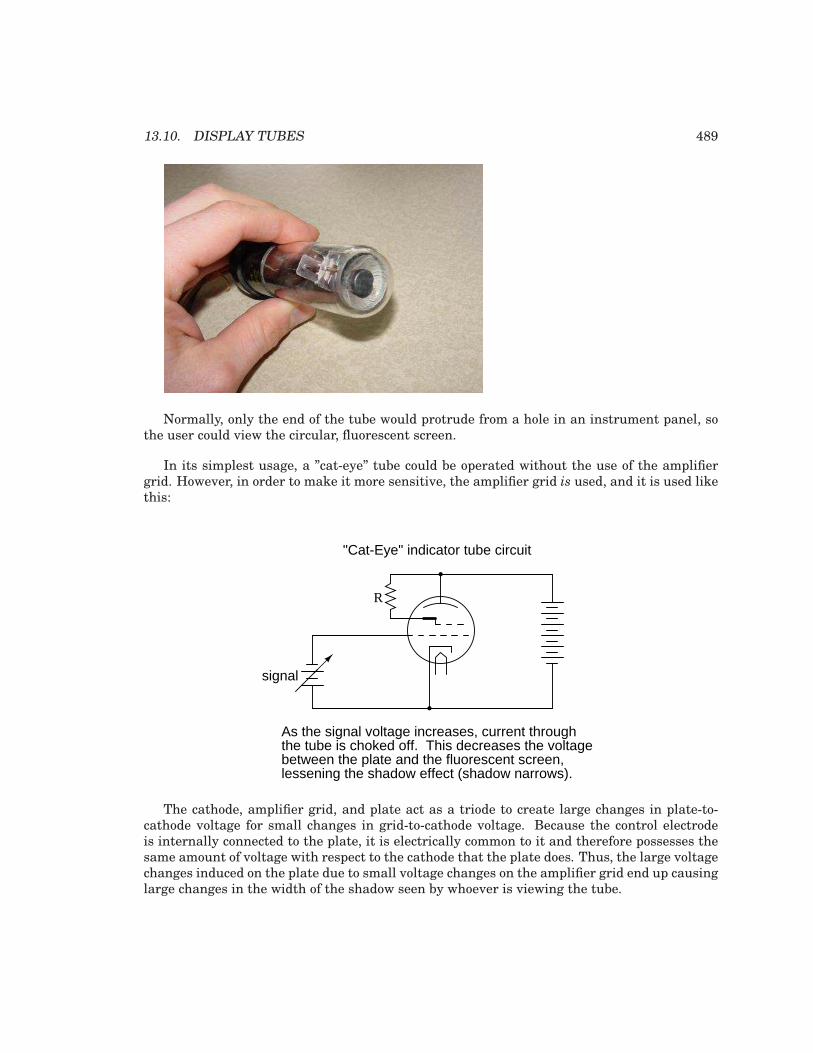
13.10. DISPLAY TUBES 489
Normally, only the end of the tube would protrude from a hole in an instrument panel, sothe user could view the circular, fluorescent screen.
In its simplest usage, a ”cat-eye” tube could be operated without the use of the amplifiergrid. However, in order to make it more sensitive, the amplifier grid is used, and it is used likethis:
R
signal
As the signal voltage increases, current through
"Cat-Eye" indicator tube circuit
the tube is choked off. This decreases the voltage
lessening the shadow effect (shadow narrows). between the plate and the fluorescent screen,
The cathode, amplifier grid, and plate act as a triode to create large changes in plate-to-cathode voltage for small changes in grid-to-cathode voltage. Because the control electrodeis internally connected to the plate, it is electrically common to it and therefore possesses thesame amount of voltage with respect to the cathode that the plate does. Thus, the large voltagechanges induced on the plate due to small voltage changes on the amplifier grid end up causinglarge changes in the width of the shadow seen by whoever is viewing the tube.
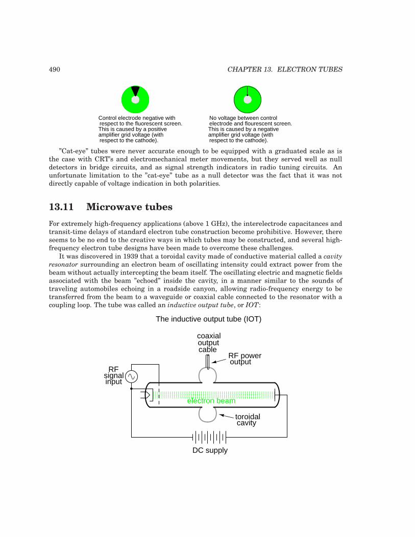
490 CHAPTER 13. ELECTRON TUBES
Control electrode negative with
This is caused by a positive amplifier grid voltage (with respect to the cathode).
This is caused by a negativeamplifier grid voltage (with respect to the cathode).
respect to the fluorescent screen.No voltage between controlelectrode and flourescent screen.
”Cat-eye” tubes were never accurate enough to be equipped with a graduated scale as isthe case with CRT’s and electromechanical meter movements, but they served well as nulldetectors in bridge circuits, and as signal strength indicators in radio tuning circuits. Anunfortunate limitation to the ”cat-eye” tube as a null detector was the fact that it was notdirectly capable of voltage indication in both polarities.
13.11 Microwave tubes
For extremely high-frequency applications (above 1 GHz), the interelectrode capacitances andtransit-time delays of standard electron tube construction become prohibitive. However, thereseems to be no end to the creative ways in which tubes may be constructed, and several high-frequency electron tube designs have been made to overcome these challenges.
It was discovered in 1939 that a toroidal cavity made of conductive material called a cavity
resonator surrounding an electron beam of oscillating intensity could extract power from thebeam without actually intercepting the beam itself. The oscillating electric and magnetic fieldsassociated with the beam ”echoed” inside the cavity, in a manner similar to the sounds oftraveling automobiles echoing in a roadside canyon, allowing radio-frequency energy to betransferred from the beam to a waveguide or coaxial cable connected to the resonator with acoupling loop. The tube was called an inductive output tube, or IOT:
DC supply
RFsignalinput
toroidal cavity
coaxialoutputcable
electron beam
RF power output
The inductive output tube (IOT)
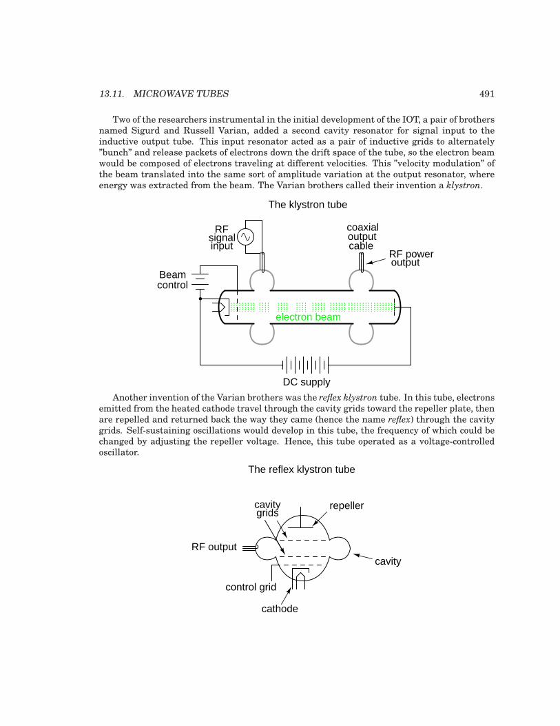
13.11. MICROWAVE TUBES 491
Two of the researchers instrumental in the initial development of the IOT, a pair of brothersnamed Sigurd and Russell Varian, added a second cavity resonator for signal input to theinductive output tube. This input resonator acted as a pair of inductive grids to alternately”bunch” and release packets of electrons down the drift space of the tube, so the electron beamwould be composed of electrons traveling at different velocities. This ”velocity modulation” ofthe beam translated into the same sort of amplitude variation at the output resonator, whereenergy was extracted from the beam. The Varian brothers called their invention a klystron.
DC supply
RFsignalinput
coaxialoutputcable
electron beam
RF power output
The klystron tube
Beamcontrol
Another invention of the Varian brothers was the reflex klystron tube. In this tube, electronsemitted from the heated cathode travel through the cavity grids toward the repeller plate, thenare repelled and returned back the way they came (hence the name reflex) through the cavitygrids. Self-sustaining oscillations would develop in this tube, the frequency of which could bechanged by adjusting the repeller voltage. Hence, this tube operated as a voltage-controlledoscillator.
repeller
RF outputcavity
cathode
cavitygrids
control grid
The reflex klystron tube
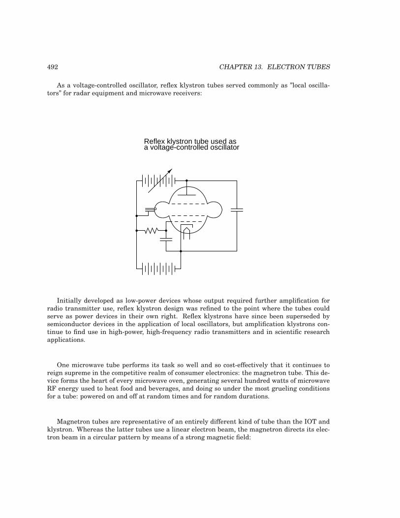
492 CHAPTER 13. ELECTRON TUBES
As a voltage-controlled oscillator, reflex klystron tubes served commonly as ”local oscilla-tors” for radar equipment and microwave receivers:
Reflex klystron tube used asa voltage-controlled oscillator
Initially developed as low-power devices whose output required further amplification forradio transmitter use, reflex klystron design was refined to the point where the tubes couldserve as power devices in their own right. Reflex klystrons have since been superseded bysemiconductor devices in the application of local oscillators, but amplification klystrons con-tinue to find use in high-power, high-frequency radio transmitters and in scientific researchapplications.
One microwave tube performs its task so well and so cost-effectively that it continues toreign supreme in the competitive realm of consumer electronics: the magnetron tube. This de-vice forms the heart of every microwave oven, generating several hundred watts of microwaveRF energy used to heat food and beverages, and doing so under the most grueling conditionsfor a tube: powered on and off at random times and for random durations.
Magnetron tubes are representative of an entirely different kind of tube than the IOT andklystron. Whereas the latter tubes use a linear electron beam, the magnetron directs its elec-tron beam in a circular pattern by means of a strong magnetic field:
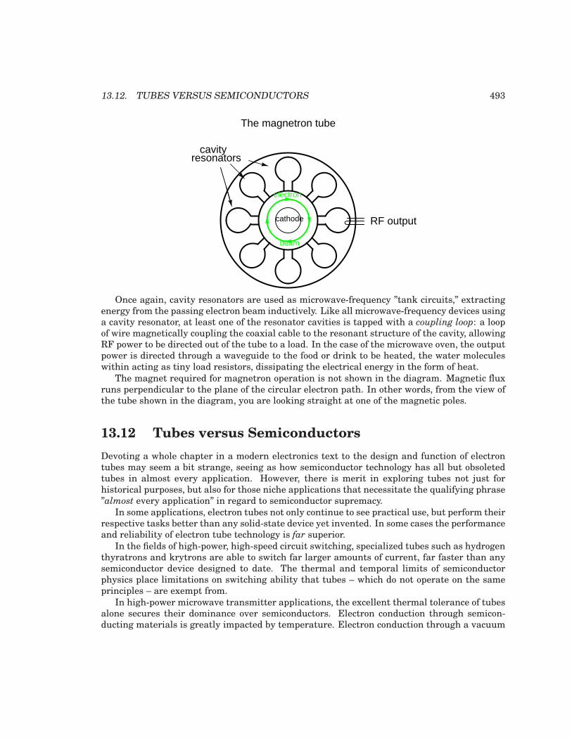
13.12. TUBES VERSUS SEMICONDUCTORS 493
cathode
electron
beam
cavityresonators
RF output
The magnetron tube
Once again, cavity resonators are used as microwave-frequency ”tank circuits,” extractingenergy from the passing electron beam inductively. Like all microwave-frequency devices usinga cavity resonator, at least one of the resonator cavities is tapped with a coupling loop: a loopof wire magnetically coupling the coaxial cable to the resonant structure of the cavity, allowingRF power to be directed out of the tube to a load. In the case of the microwave oven, the outputpower is directed through a waveguide to the food or drink to be heated, the water moleculeswithin acting as tiny load resistors, dissipating the electrical energy in the form of heat.
The magnet required for magnetron operation is not shown in the diagram. Magnetic fluxruns perpendicular to the plane of the circular electron path. In other words, from the view ofthe tube shown in the diagram, you are looking straight at one of the magnetic poles.
13.12 Tubes versus Semiconductors
Devoting a whole chapter in a modern electronics text to the design and function of electrontubes may seem a bit strange, seeing as how semiconductor technology has all but obsoletedtubes in almost every application. However, there is merit in exploring tubes not just forhistorical purposes, but also for those niche applications that necessitate the qualifying phrase”almost every application” in regard to semiconductor supremacy.
In some applications, electron tubes not only continue to see practical use, but perform theirrespective tasks better than any solid-state device yet invented. In some cases the performanceand reliability of electron tube technology is far superior.
In the fields of high-power, high-speed circuit switching, specialized tubes such as hydrogenthyratrons and krytrons are able to switch far larger amounts of current, far faster than anysemiconductor device designed to date. The thermal and temporal limits of semiconductorphysics place limitations on switching ability that tubes – which do not operate on the sameprinciples – are exempt from.
In high-power microwave transmitter applications, the excellent thermal tolerance of tubesalone secures their dominance over semiconductors. Electron conduction through semicon-ducting materials is greatly impacted by temperature. Electron conduction through a vacuum
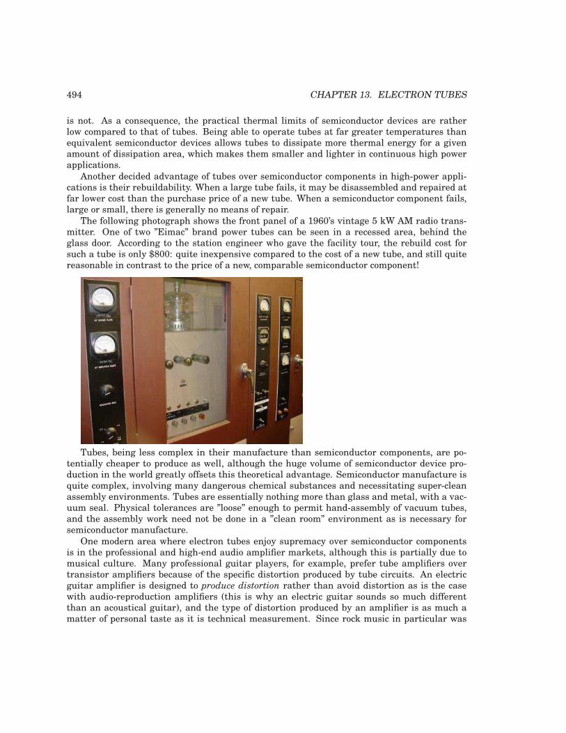
494 CHAPTER 13. ELECTRON TUBES
is not. As a consequence, the practical thermal limits of semiconductor devices are ratherlow compared to that of tubes. Being able to operate tubes at far greater temperatures thanequivalent semiconductor devices allows tubes to dissipate more thermal energy for a givenamount of dissipation area, which makes them smaller and lighter in continuous high powerapplications.
Another decided advantage of tubes over semiconductor components in high-power appli-cations is their rebuildability. When a large tube fails, it may be disassembled and repaired atfar lower cost than the purchase price of a new tube. When a semiconductor component fails,large or small, there is generally no means of repair.
The following photograph shows the front panel of a 1960’s vintage 5 kW AM radio trans-mitter. One of two ”Eimac” brand power tubes can be seen in a recessed area, behind theglass door. According to the station engineer who gave the facility tour, the rebuild cost forsuch a tube is only $800: quite inexpensive compared to the cost of a new tube, and still quitereasonable in contrast to the price of a new, comparable semiconductor component!
Tubes, being less complex in their manufacture than semiconductor components, are po-tentially cheaper to produce as well, although the huge volume of semiconductor device pro-duction in the world greatly offsets this theoretical advantage. Semiconductor manufacture isquite complex, involving many dangerous chemical substances and necessitating super-cleanassembly environments. Tubes are essentially nothing more than glass and metal, with a vac-uum seal. Physical tolerances are ”loose” enough to permit hand-assembly of vacuum tubes,and the assembly work need not be done in a ”clean room” environment as is necessary forsemiconductor manufacture.
One modern area where electron tubes enjoy supremacy over semiconductor componentsis in the professional and high-end audio amplifier markets, although this is partially due tomusical culture. Many professional guitar players, for example, prefer tube amplifiers overtransistor amplifiers because of the specific distortion produced by tube circuits. An electricguitar amplifier is designed to produce distortion rather than avoid distortion as is the casewith audio-reproduction amplifiers (this is why an electric guitar sounds so much differentthan an acoustical guitar), and the type of distortion produced by an amplifier is as much amatter of personal taste as it is technical measurement. Since rock music in particular was
13.12. TUBES VERSUS SEMICONDUCTORS 495
born with guitarists playing tube-amplifier equipment, there is a significant level of ”tubeappeal” inherent to the genre itself, and this appeal shows itself in the continuing demand for”tubed” guitar amplifiers among rock guitarists.
As an illustration of the attitude among some guitarists, consider the following quote takenfrom the technical glossary page of a tube-amplifier website which will remain nameless:
Solid State: A component that has been specifically designed to make a guitar
amplifier sound bad. Compared to tubes, these devices can have a very long lifespan,
which guarantees that your amplifier will retain its thin, lifeless, and buzzy sound
for a long time to come.
In the area of audio reproduction amplifiers (music studio amplifiers and home entertain-ment amplifiers), it is best for an amplifier to reproduce the musical signal with as little distor-tion as possible. Paradoxically, in contrast to the guitar amplifier market where distortion is adesign goal, high-end audio is another area where tube amplifiers enjoy continuing consumerdemand. Though one might suppose the objective, technical requirement of low distortionwould eliminate any subjective bias on the part of audiophiles, one would be very wrong. Themarket for high-end ”tubed” amplifier equipment is quite volatile, changing rapidly with trendsand fads, driven by highly subjective claims of ”magical” sound from audio system reviewersand salespeople. As in the electric guitar world, there is no small measure of cult-like devotionto tube amplifiers among some quarters of the audiophile world. As an example of this irra-tionality, consider the design of many ultra-high-end amplifiers, with chassis built to displaythe working tubes openly, even though this physical exposure of the tubes obviously enhancesthe undesirable effect ofmicrophonics (changes in tube performance as a result of sound wavesvibrating the tube structure).
Having said this, though, there is a wealth of technical literature contrasting tubes againstsemiconductors for audio power amplifier use, especially in the area of distortion analysis.More than a few competent electrical engineers prefer tube amplifier designs over transistors,and are able to produce experimental evidence in support of their choice. The primary diffi-culty in quantifying audio system performance is the uncertain response of human hearing.All amplifiers distort their input signal to some degree, especially when overloaded, so thequestion is which type of amplifier design distorts the least. However, since human hearing isvery nonlinear, people do not interpret all types of acoustic distortion equally, and so some am-plifiers will sound ”better” than others even if a quantitative distortion analysis with electronicinstruments indicates similar distortion levels. To determine what type of audio amplifier willdistort a musical signal ”the least,” we must regard the human ear and brain as part of thewhole acoustical system. Since no complete model yet exists for human auditory response,objective assessment is difficult at best. However, some research indicates that the character-istic distortion of tube amplifier circuits (especially when overloaded) is less objectionable thandistortion produced by transistors.
Tubes also possess the distinct advantage of low ”drift” over a wide range of operatingconditions. Unlike semiconductor components, whose barrier voltages, β ratios, bulk resis-tances, and junction capacitances may change substantially with changes in device temper-ature and/or other operating conditions, the fundamental characteristics of a vacuum tuberemain nearly constant over a wide range in operating conditions, because those character-istics are determined primarily by the physical dimensions of the tube’s structural elements
496 CHAPTER 13. ELECTRON TUBES
(cathode, grid(s), and plate) rather than the interactions of subatomic particles in a crystallinelattice.
This is one of the major reasons solid-state amplifier designers typically engineer their cir-cuits to maximize power-efficiency even when it compromises distortion performance, becausea power-inefficient amplifier dissipates a lot of energy in the form of waste heat, and transistorcharacteristics tend to change substantially with temperature. Temperature-induced ”drift”makes it difficult to stabilize ”Q” points and other important performance-related measures inan amplifier circuit. Unfortunately, power efficiency and low distortion seem to be mutuallyexclusive design goals.
For example, class A audio amplifier circuits typically exhibit very low distortion levels, butare very wasteful of power, meaning that it would be difficult to engineer a solid-state class Aamplifier of any substantial power rating due to the consequent drift of transistor characteris-tics. Thus, most solid-state audio amplifier designers choose class B circuit configurations forgreater efficiency, even though class B designs are notorious for producing a type of distortionknown as crossover distortion. However, with tubes it is easy to design a stable class A audioamplifier circuit because tubes are not as adversely affected by the changes in temperatureexperienced in a such a power-inefficient circuit configuration.
Tube performance parameters, though, tend to ”drift” more than semiconductor deviceswhen measured over long periods of time (years). One major mechanism of tube ”aging” ap-pears to be vacuum leaks: when air enters the inside of a vacuum tube, its electrical character-istics become irreversibly altered. This same phenomenon is a major cause of tube mortality,or why tubes typically do not last as long as their respective solid-state counterparts. Whentube vacuum is maintained at a high level, though, excellent performance and life is possible.An example of this is a klystron tube (used to produce the high-frequency radio waves used ina radar system) that lasted for 240,000 hours of operation (cited by Robert S. Symons of LittonElectron Devices Division in his informative paper, ”Tubes: Still vital after all these years,”printed in the April 1998 issue of IEEE Spectrum magazine).
If nothing else, the tension between audiophiles over tubes versus semiconductors hasspurred a remarkable degree of experimentation and technical innovation, serving as an ex-cellent resource for those wishing to educate themselves on amplifier theory. Taking a widerview, the versatility of electron tube technology (different physical configurations, multiplecontrol grids) hints at the potential for circuit designs of far greater variety than is possibleusing semiconductors. For this and other reasons, electron tubes will never be ”obsolete,” butwill continue to serve in niche roles, and to foster innovation for those electronics engineers,inventors, and hobbyists who are unwilling to let their minds by stifled by convention.
Appendix A-1
ABOUT THIS BOOK
A-1.1 Purpose
They say that necessity is the mother of invention. At least in the case of this book, that adageis true. As an industrial electronics instructor, I was forced to use a sub-standard textbookduring my first year of teaching. My students were daily frustrated with the many typograph-ical errors and obscure explanations in this book, having spent much time at home strugglingto comprehend the material within. Worse yet were the many incorrect answers in the back ofthe book to selected problems. Adding insult to injury was the $100+ price.
Contacting the publisher proved to be an exercise in futility. Even though the particulartext I was using had been in print and in popular use for a couple of years, they claimed mycomplaint was the first they’d ever heard. My request to review the draft for the next editionof their book was met with disinterest on their part, and I resolved to find an alternative text.
Finding a suitable alternative was more difficult than I had imagined. Sure, there wereplenty of texts in print, but the really good books seemed a bit too heavy on the math and theless intimidating books omitted a lot of information I felt was important. Some of the bestbooks were out of print, and those that were still being printed were quite expensive.
It was out of frustration that I compiled Lessons in Electric Circuits from notes and ideas Ihad been collecting for years. My primary goal was to put readable, high-quality informationinto the hands of my students, but a secondary goal was to make the book as affordable aspossible. Over the years, I had experienced the benefit of receiving free instruction and encour-agement in my pursuit of learning electronics from many people, including several teachersof mine in elementary and high school. Their selfless assistance played a key role in my ownstudies, paving the way for a rewarding career and fascinating hobby. If only I could extendthe gift of their help by giving to other people what they gave to me . . .
So, I decided to make the book freely available. More than that, I decided to make it ”open,”following the same development model used in the making of free software (most notably thevarious UNIX utilities released by the Free Software Foundation, and the Linux operating
497
498 APPENDIX A-1. ABOUT THIS BOOK
system, whose fame is growing even as I write). The goal was to copyright the text – so as toprotect my authorship – but expressly allow anyone to distribute and/or modify the text to suittheir own needs with a minimum of legal encumbrance. This willful and formal revoking ofstandard distribution limitations under copyright is whimsically termed copyleft. Anyone can”copyleft” their creative work simply by appending a notice to that effect on their work, butseveral Licenses already exist, covering the fine legal points in great detail.
The first such License I applied to my work was the GPL – General Public License – of theFree Software Foundation (GNU). The GPL, however, is intended to copyleft works of computersoftware, and although its introductory language is broad enough to cover works of text, itswording is not as clear as it could be for that application. When other, less specific copyleftLicenses began appearing within the free software community, I chose one of them (the DesignScience License, or DSL) as the official notice for my project.
In ”copylefting” this text, I guaranteed that no instructor would be limited by a text insuffi-cient for their needs, as I had been with error-ridden textbooks from major publishers. I’m surethis book in its initial form will not satisfy everyone, but anyone has the freedom to change it,leveraging my efforts to suit variant and individual requirements. For the beginning studentof electronics, learn what you can from this book, editing it as you feel necessary if you comeacross a useful piece of information. Then, if you pass it on to someone else, you will be givingthem something better than what you received. For the instructor or electronics professional,feel free to use this as a reference manual, adding or editing to your heart’s content. Theonly ”catch” is this: if you plan to distribute your modified version of this text, you must givecredit where credit is due (to me, the original author, and anyone else whose modifications arecontained in your version), and you must ensure that whoever you give the text to is aware oftheir freedom to similarly share and edit the text. The next chapter covers this process in moredetail.
It must be mentioned that although I strive to maintain technical accuracy in all of thisbook’s content, the subject matter is broad and harbors many potential dangers. Electricitymaims and kills without provocation, and deserves the utmost respect. I strongly encourageexperimentation on the part of the reader, but only with circuits powered by small batterieswhere there is no risk of electric shock, fire, explosion, etc. High-power electric circuits shouldbe left to the care of trained professionals! The Design Science License clearly states thatneither I nor any contributors to this book bear any liability for what is done with its contents.
A-1.2 The use of SPICE
One of the best ways to learn how things work is to follow the inductive approach: to observespecific instances of things working and derive general conclusions from those observations.In science education, labwork is the traditionally accepted venue for this type of learning, al-though in many cases labs are designed by educators to reinforce principles previously learnedthrough lecture or textbook reading, rather than to allow the student to learn on their ownthrough a truly exploratory process.
Having taught myself most of the electronics that I know, I appreciate the sense of frustra-tion students may have in teaching themselves from books. Although electronic componentsare typically inexpensive, not everyone has the means or opportunity to set up a laboratoryin their own homes, and when things go wrong there’s no one to ask for help. Most textbooks
A-1.3. ACKNOWLEDGEMENTS 499
seem to approach the task of education from a deductive perspective: tell the student howthings are supposed to work, then apply those principles to specific instances that the studentmay or may not be able to explore by themselves. The inductive approach, as useful as it is, ishard to find in the pages of a book.
However, textbooks don’t have to be this way. I discovered this when I started to learn acomputer program called SPICE. It is a text-based piece of software intended to model circuitsand provide analyses of voltage, current, frequency, etc. Although nothing is quite as good asbuilding real circuits to gain knowledge in electronics, computer simulation is an excellent al-ternative. In learning how to use this powerful tool, I made a discovery: SPICE could be usedwithin a textbook to present circuit simulations to allow students to ”observe” the phenomenafor themselves. This way, the readers could learn the concepts inductively (by interpretingSPICE’s output) as well as deductively (by interpreting my explanations). Furthermore, inseeing SPICE used over and over again, they should be able to understand how to use it them-selves, providing a perfectly safe means of experimentation on their own computers with circuitsimulations of their own design.
Another advantage to including computer analyses in a textbook is the empirical verifi-cation it adds to the concepts presented. Without demonstrations, the reader is left to takethe author’s statements on faith, trusting that what has been written is indeed accurate. Theproblem with faith, of course, is that it is only as good as the authority in which it is placed andthe accuracy of interpretation through which it is understood. Authors, like all human beings,are liable to err and/or communicate poorly. With demonstrations, however, the reader canimmediately see for themselves that what the author describes is indeed true. Demonstrationsalso serve to clarify the meaning of the text with concrete examples.
SPICE is introduced early in volume I (DC) of this book series, and hopefully in a gentleenough way that it doesn’t create confusion. For those wishing to learn more, a chapter inthe Reference volume (volume V) contains an overview of SPICE with many example circuits.There may be more flashy (graphic) circuit simulation programs in existence, but SPICE isfree, a virtue complementing the charitable philosophy of this book very nicely.
A-1.3 Acknowledgements
First, I wish to thank my wife, whose patience during those many and long evenings (andweekends!) of typing has been extraordinary.
I also wish to thank those whose open-source software development efforts have made thisendeavor all the more affordable and pleasurable. The following is a list of various free com-puter software used to make this book, and the respective programmers:
• GNU/Linux Operating System – Linus Torvalds, Richard Stallman, and a host of otherstoo numerous to mention.
• Vim text editor – Bram Moolenaar and others.
• Xcircuit drafting program – Tim Edwards.
• SPICE circuit simulation program – too many contributors to mention.
• TEX text processing system – Donald Knuth and others.
500 APPENDIX A-1. ABOUT THIS BOOK
• Texinfo document formatting system – Free Software Foundation.
• LATEX document formatting system – Leslie Lamport and others.
• Gimp image manipulation program – too many contributors to mention.
Appreciation is also extended to Robert L. Boylestad, whose first edition of IntroductoryCircuit Analysis taught me more about electric circuits than any other book. Other importanttexts in my electronics studies include the 1939 edition of The ”Radio” Handbook, BernardGrob’s second edition of Introduction to Electronics I, and Forrest Mims’ original Engineer’sNotebook.
Thanks to the staff of the Bellingham Antique Radio Museum, who were generous enoughto let me terrorize their establishment with my camera and flash unit.
I wish to specifically thank Jeffrey Elkner and all those at Yorktown High School for beingwilling to host my book as part of their Open Book Project, and to make the first effort in con-tributing to its form and content. Thanks also to David Sweet (website: (http://www.andamooka.org) )and Ben Crowell (website: (http://www.lightandmatter.com) ) for providing encourage-ment, constructive criticism, and a wider audience for the online version of this book.
Thanks to Michael Stutz for drafting his Design Science License, and to Richard Stallmanfor pioneering the concept of copyleft.
Last but certainly not least, many thanks to my parents and those teachers of mine whosaw in me a desire to learn about electricity, and who kindled that flame into a passion fordiscovery and intellectual adventure. I honor you by helping others as you have helped me.
Tony Kuphaldt, July 2001
”A candle loses nothing of its light when lighting another”
Kahlil Gibran

Appendix A-2
CONTRIBUTOR LIST
A-2.1 How to contribute to this book
As a copylefted work, this book is open to revision and expansion by any interested parties.The only ”catch” is that credit must be given where credit is due. This is a copyrighted work:it is not in the public domain!
If you wish to cite portions of this book in a work of your own, you must follow the sameguidelines as for any other copyrighted work. Here is a sample from the Design Science Li-cense:
The Work is copyright the Author. All rights to the Work are re servedby the Author, except as specifically described below. This Licensedescribes the terms and conditions under which the Author pe rmits youto copy, distribute and modify copies of the Work.
In addition, you may refer to the Work, talk about it, and (asdictated by "fair use") quote from it, just as you would anycopyrighted material under copyright law.
Your right to operate, perform, read or otherwise interpret and/orexecute the Work is unrestricted; however, you do so at your o wn risk,because the Work comes WITHOUT ANY WARRANTY -- see Section 7 ( "NOWARRANTY") below.
If you wish to modify this book in any way, you must document the nature of those modifi-cations in the ”Credits” section along with your name, and ideally, information concerning howyou may be contacted. Again, the Design Science License:
Permission is granted to modify or sample from a copy of the Wo rk,
501
502 APPENDIX A-2. CONTRIBUTOR LIST
producing a derivative work, and to distribute the derivati ve workunder the terms described in the section for distribution ab ove,provided that the following terms are met:
(a) The new, derivative work is published under the terms of t hisLicense.
(b) The derivative work is given a new name, so that its name ortitle can not be confused with the Work, or with a version ofthe Work, in any way.
(c) Appropriate authorship credit is given: for the differe ncesbetween the Work and the new derivative work, authorship isattributed to you, while the material sampled or used fromthe Work remains attributed to the original Author; appropr iatenotice must be included with the new work indicating the natu reand the dates of any modifications of the Work made by you.
Given the complexities and security issues surrounding the maintenance of files comprisingthis book, it is recommended that you submit any revisions or expansions to the original author(Tony R. Kuphaldt). You are, of course, welcome to modify this book directly by editing yourown personal copy, but we would all stand to benefit from your contributions if your ideas wereincorporated into the online “master copy” where all the world can see it.
A-2.2 Credits
All entries arranged in alphabetical order of surname. Major contributions are listed by indi-vidual name with some detail on the nature of the contribution(s), date, contact info, etc. Minorcontributions (typo corrections, etc.) are listed by name only for reasons of brevity. Please un-derstand that when I classify a contribution as “minor,” it is in no way inferior to the effortor value of a “major” contribution, just smaller in the sense of less text changed. Any and allcontributions are gratefully accepted. I am indebted to all those who have given freely of theirown knowledge, time, and resources to make this a better book!
A-2.2.1 Tony R. Kuphaldt
• Date(s) of contribution(s): 1996 to present
• Nature of contribution: Original author.
• Contact at: [email protected]
A-2.2. CREDITS 503
A-2.2.2 Dennis Crunkilton
• Date(s) of contribution(s): July 2004 to present
• Nature of contribution: Mini table of contents, all chapters except appendicies; html,latex, ps, pdf; See Devel/tutorial.html; 01/2006.
• Nature of contribution: Completed Ch4 Bipolar junction transistors, CH7 Thyristors;Ch9 Practical anlog ckts, a few additions; Ch8 Opamps, minor; 04/2009
• Contact at: dcrunkilton(at)att(dot)net
A-2.2.3 Bill Marsden
• Date(s) of contribution(s): May 2003 - present
• Nature of contribution: Update to LED subsection, Diodes Ch 3 , Nov 2003.
• Nature of contribution: Original author: “ElectroStatic Discharge” Section, Chapter9, May 2008.
• Nature of contribution: Chapter 3, LED’s update, photodiode update, Feburary 2009.
• Nature of contribution: Chapter 11, Section author: ”Pulse Width Modulation”, Febu-rary 2010.
• Contact at: bill marsden2(at)hotmail(dot)com
A-2.2.4 John Anhalt
• Date(s) of contribution(s): June 2011
• Nature of contribution: Updated Si SP3 electron hybridization, Ch 2
• Contact at: [email protected]
A-2.2.5 Your name here
• Date(s) of contribution(s): Month and year of contribution
• Nature of contribution: Insert text here, describing how you contributed to the book.
• Contact at: my [email protected]

504 APPENDIX A-2. CONTRIBUTOR LIST
A-2.2.6 Typo corrections and other “minor” contributions
• line-allaboutcircuits.com (June 2005) Typographical error correction in Volumes 1,2,3,5,various chapters ,(:s/visa-versa/vice versa/).
• Colin Creitz (May 2007) Chapters: several, s/it’s/its.
• Dennis Crunkilton (October 2005) Typographical capitlization correction to sectionti-tles, chapter 9.
• Jeff DeFreitas (March 2006)Improve appearance: replace “/” and ”/” Chapters: A1, A2.
• Paul Stokes, Program Chair, Computer and Electronics Engineering Technology, ITTTechnical Institute, Houston, Tx (October 2004) Change (10012 = -810 + 710 = -110) to(10012 = -810 + 110 = -110), CH2, Binary Arithmetic
• Paul Stokes, Program Chair Computer and Electronics Engineering Technology, ITTTechnical Institute, Houston, Tx (October 2004) Near ”Fold up the corners” change Out=B’C’to Out=B’D’, 14118.eps same change, Karnaugh Mapping
• The students of Bellingham Technical College’s Instrumentation program, .
• Roger Hollingsworth (May 2003) Suggested a way to make the PLC motor controlsystem fail-safe.
• Jan-Willem Rensman (May 2002) Suggested the inclusion of Schmitt triggers and gatehysteresis to the ”Logic Gates” chapter.
• Don Stalkowski (June 2002) Technical help with PostScript-to-PDF file format conver-sion.
• Joseph Teichman (June 2002) Suggestion and technical help regarding use of PNGimages instead of JPEG.
• [email protected] (November 2007) “Boolean algebra”, images 14019.pes14021.eps output of gates incorrect s/0/A s/1/A .
• Dan Simon (February 2008) “Numeration Systems”, After BINARY TO OCTAL CON-VERSION, position of decimal point —.
• Timothy Kingman (March 2008) Changed default roman font to newcent.
• Imranullah Syed (March 2008) Suggested centering of uncaptioned schematics.
• [email protected] (March 2008) Ch 15, Inaccuracy involving CD-ROMproduction.
• [email protected] (March 2008) Ch 15, s/disk/disc/ in CDROM .
• [email protected] (April 2008) Ch 12, s/laralel-out/parallel-out/ .
• Ken Braswell (May 2008) Ch 3, s/drips/drops/.
A-2.2. CREDITS 505
• [email protected] (Oct 2008) Ch 2, s/are in close/are close/.
• [email protected] (Oct 2008) Ch 8, s/that 1 mA of/that 6 mA/.
• [email protected] (Dec 2008) Ch 2, s/shells are hold/shells hold/.
• [email protected] (Dec 2008) Ch 7, image 03320.png, swapped anode andanode gate. left diagram.
• Unregistered [email protected] (Feb 2009) Ch 2 s/than FET’s/than JFET’s.
• Unregistered [email protected] (March 2009) Ch 8, 13061.png, changeformula for inverting gain to include ”-” .
• [email protected] (March 2009) Ch 3, 03443.png, s/p-p/peak.
• Bill [email protected] (April 2009) Ch 3, s/I would/It would/
• Peter [email protected] (April 2009) Ch 1, closing parenthesis, above replacedwith reference to figure.
• [email protected] (April 2009) Ch 9, image 53009.jpg s/courtisy/courtesy.
• Bill [email protected] (April 2009) Ch 8, images 2001.png, 2002.pngappearance.
• D Crunkilton (April 2009) Ch 4, images 23006.png, 23007.png updated.
• Unregistered [email protected] (June 2009) Ch 7, s/SCR schematic sym-bol/TRIAC schematic symbol .
• Peter O’Dette (June 2009) Ch 1, s/is 1 watts/is 1 Watt , s/10 watt/10 Watts , s/ watt/ Watt.
• Unregistered [email protected] (June 2009) Ch 3, s/being/begin , near”voltage at which they” . s/is/in near ”The diodes must be”.
• [email protected] (June 2009) Ch 4, s/r1 1 2 1/r1 1 2 1k in common-emitter amplifier SPICE list.
• Unregistered [email protected] (July 2009) Ch 3, s/Note polarity changeon coil changed/Note polarity change on coil.
• Unregistered [email protected] (August 2009) Ch 4, Swap PNP & NPN at(b) & (c), caption of 03075.png .
• Unregistered [email protected] (August 2009) equation typos 03077.png03479.png .
• Peter O’[email protected] (August 2009) Ch 2, Numerous changes, and03409.png .

506 APPENDIX A-2. CONTRIBUTOR LIST
• Bill [email protected] (November 2009) Ch 4, Beta formula, ”Transistoratings and Packages”.
• Unregistered [email protected] (November 2009) Ch 3, Image 03288.epschanged polarized capacitor to non-polarized.
• Unregistered [email protected] (November 2009) Ch 4 s/hasre/share/ s/common=emitter/common-emitter/ .
• [email protected] (November 2009) Ch 3, s/once every half-cycle/one half ofevery full cycle/ , s/much/half/ .
• Unregistered [email protected] (November 2009) Ch 4 s/To maintaining/Tomaintain .
• Unregistered [email protected] (November 2009) Ch 3 s/[model]/[modelname]/.
• [email protected] (November 2009) Ch 2 numerous typos, omis-sions .
• [email protected] (November 2009) Ch 2 minor chages to text andimage 03392.eps .
• [email protected] (December 2009) Ch 4 equations 4 and 7 of image03488.eps .
• [email protected] (January 2010) Ch 7 s/will will/will/ .
• [email protected] (February 2010) Ch 1, Clarification of text between im-ages 03378.png and 03379.png .
• [email protected] (March 2010) Ch 4, image 03375.png, flipped pnpand battery .
• Bill [email protected] (March 2010) Ch 9, Changes to ESD section.
• [email protected] (April 2010) Ch 4, image 03078.png, added resis-tors.
• [email protected] (April 2010) Ch 4, typo in SPICE listing near im-age 20004.png.
• [email protected] (July 2010) Ch 2, typo s/campared/compared/.
• Bill [email protected] (July 2010) Ch 11, change [I] to italic tags in dc-drive.sml .
• Unregistered guest @allaboutcircuits.com (August 2010) Ch 2, s/The bopolar tran-sistor/The bipolar junction transistor/ .
• Unregistered guest @allaboutcircuits.com (August 2010) Ch 4,

A-2.2. CREDITS 507
• D Crunkilton (Sept 2010) Ch 2 s/minuscule/minuscule; Ch 3 ,4 ,5, 7, s/useable/usable.
• [email protected] (Oct 2010) Ch 3, AC line powered LED material re-moved.
• [email protected] (Feb 2011) Ch 3, s/5 Vptp/10 Vptp/
• [email protected] (Feb 2011) Ch 1, s/ ource/source/
• [email protected] (Feb 2011) Ch 2, 4, A3 s/the the/the/
• [email protected] (Feb 2011) Ch 2, s/insulator insulator/insulator/
• [email protected] (Feb 2011) Ch 3, s/a approximately/at approximately/ ,s/frequency my/frequency may/ , s/application a/appliation is as/ , s/been produce/beenproduced/; Ch4 s/approximage/approximate/ s/resistor is a short/capacitor is a short/ ;s/Iis it/Is it/ s/The the/The/ s/the these/these/, s/distortion distortion/distortion/
• D. Crunkilton (June 2011) hi.latex, header file; updated link to openbookproject.net .
• [email protected] (May 2012) Ch 2 s/occurr/occur s/repells/repels/ , s/isincreases/increases , at (c) changed to full reference, .
• [email protected] (May 2012) Ch 4, various
• Bill [email protected] (May 2012) Ch 4, Clarification of text near: Bipo-lar transistors are contructed. . ..
• [email protected] (January 2013) Ch 4,image 03495.eps corrected. AddedOhm symbol to 0.26, above 2600 Ohm.
• [email protected] (January 2013) Ch 4, caption image 03495.png s/resistanceVth/resistance Rth.
• [email protected] (January 2013) Ch 4, caption image 03495.pngs/resistance Vth/resistance Rth.
• Eugene Smirnoff (January 2013) Ch 2, near ”A SQUID’” s/is an/is a/ s/Superconduction/Superconducting.
• [email protected] (February 2014) Ch 3, s/inversely proportional/iverted/in Common Emitter section .
• [email protected] (February 2014) Ch 1,symbol for neper s/n/Np/. Ch2, s/Dimitri/Dmitri/, s/always”risky”/always ”risky”/
• triffid [email protected] (February 2014) Ch 3, s/common-base/common-emitter , caption and image 03502.eps in Cascode section .
• [email protected] (February 2014) Ch 4, s/RB/RE in table near image 03488.pngand in image 03488.png

508 APPENDIX A-2. CONTRIBUTOR LIST
• [email protected] (February 2014) Ch 4, change b to Beta in image 03488.png;above 13074.png s/base resistor/emitter resistor. After internal resistance: s/RE/REE.s+(Beta)REE/IE+(Beta)REE+.
• [email protected] (February 2014) Ch 4, change 22 instance of REE to ree intext; same for images: 03489.eps 03494.eps 03495.eps 03497.eps 13062.eps
• [email protected] (February 2014) Ch 4, insert bigspcace tag above By-pass Capacitor for R.
• [email protected] (February 2014) Ch 4, s/Small emitter base currentcontrols large collector emitter current flowing against emitter arrow/Small Base-Emittercurrent controls large Collector-Emitter current flowing against emitter arrow/. im-age:13048.eps changed Euler’s constant to Euler’s Number.
• [email protected] (February 2014) Ch 3, insert missing image 03300.pnginto diode.sml.
• RomanKaluzniacki (October 2014) Ch 2, s/principle/principal with respect to ”principalquantum number”.
• va-sawyer (August 2015) Ch 4, s/0.26mV/26m/ s/Re’/rEE/.
Appendix A-3
DESIGN SCIENCE LICENSE
Copyright c© 1999-2000 Michael Stutz [email protected] copying of this document is permitted, in any medium.
A-3.1 0. Preamble
Copyright law gives certain exclusive rights to the author of a work, including the rightsto copy, modify and distribute the work (the ”reproductive,” ”adaptative,” and ”distribution”rights).
The idea of ”copyleft” is to willfully revoke the exclusivity of those rights under certainterms and conditions, so that anyone can copy and distribute the work or properly attributedderivative works, while all copies remain under the same terms and conditions as the original.
The intent of this license is to be a general ”copyleft” that can be applied to any kind of workthat has protection under copyright. This license states those certain conditions under whicha work published under its terms may be copied, distributed, and modified.
Whereas ”design science” is a strategy for the development of artifacts as a way to reformthe environment (not people) and subsequently improve the universal standard of living, thisDesign Science License was written and deployed as a strategy for promoting the progress ofscience and art through reform of the environment.
A-3.2 1. Definitions
”License” shall mean this Design Science License. The License applies to any work whichcontains a notice placed by the work’s copyright holder stating that it is published under theterms of this Design Science License.
”Work” shall mean such an aforementioned work. The License also applies to the output ofthe Work, only if said output constitutes a ”derivative work” of the licensed Work as defined bycopyright law.
509
510 APPENDIX A-3. DESIGN SCIENCE LICENSE
”Object Form” shall mean an executable or performable form of the Work, being an embod-iment of the Work in some tangible medium.
”Source Data” shall mean the origin of the Object Form, being the entire, machine-readable,preferred form of the Work for copying and for human modification (usually the language,encoding or format in which composed or recorded by the Author); plus any accompanyingfiles, scripts or other data necessary for installation, configuration or compilation of the Work.
(Examples of ”Source Data” include, but are not limited to, the following: if the Work isan image file composed and edited in ’PNG’ format, then the original PNG source file is theSource Data; if the Work is an MPEG 1.0 layer 3 digital audio recording made from a ’WAV’format audio file recording of an analog source, then the original WAV file is the Source Data;if the Work was composed as an unformatted plaintext file, then that file is the Source Data; ifthe Work was composed in LaTeX, the LaTeX file(s) and any image files and/or custom macrosnecessary for compilation constitute the Source Data.)
”Author” shall mean the copyright holder(s) of the Work.
The individual licensees are referred to as ”you.”
A-3.3 2. Rights and copyright
The Work is copyright the Author. All rights to the Work are reserved by the Author, except asspecifically described below. This License describes the terms and conditions under which theAuthor permits you to copy, distribute and modify copies of the Work.
In addition, you may refer to the Work, talk about it, and (as dictated by ”fair use”) quotefrom it, just as you would any copyrighted material under copyright law.
Your right to operate, perform, read or otherwise interpret and/or execute the Work is un-restricted; however, you do so at your own risk, because the Work comes WITHOUT ANYWARRANTY – see Section 7 (”NO WARRANTY”) below.
A-3.4 3. Copying and distribution
Permission is granted to distribute, publish or otherwise present verbatim copies of the entireSource Data of the Work, in any medium, provided that full copyright notice and disclaimer ofwarranty, where applicable, is conspicuously published on all copies, and a copy of this Licenseis distributed along with the Work.
Permission is granted to distribute, publish or otherwise present copies of the Object Formof the Work, in any medium, under the terms for distribution of Source Data above and alsoprovided that one of the following additional conditions are met:
(a) The Source Data is included in the same distribution, distributed under the terms ofthis License; or
(b) A written offer is included with the distribution, valid for at least three years or foras long as the distribution is in print (whichever is longer), with a publicly-accessible address(such as a URL on the Internet) where, for a charge not greater than transportation and mediacosts, anyone may receive a copy of the Source Data of the Work distributed according to thesection above; or
A-3.5. 4. MODIFICATION 511
(c) A third party’s written offer for obtaining the Source Data at no cost, as described inparagraph (b) above, is included with the distribution. This option is valid only if you are anon-commercial party, and only if you received the Object Form of the Work along with suchan offer.
You may copy and distribute the Work either gratis or for a fee, and if desired, you mayoffer warranty protection for the Work.
The aggregation of the Work with other works which are not based on the Work – such asbut not limited to inclusion in a publication, broadcast, compilation, or other media – does notbring the other works in the scope of the License; nor does such aggregation void the terms ofthe License for the Work.
A-3.5 4. Modification
Permission is granted to modify or sample from a copy of the Work, producing a derivativework, and to distribute the derivative work under the terms described in the section for distri-bution above, provided that the following terms are met:
(a) The new, derivative work is published under the terms of this License.
(b) The derivative work is given a new name, so that its name or title can not be confusedwith the Work, or with a version of the Work, in any way.
(c) Appropriate authorship credit is given: for the differences between the Work and thenew derivative work, authorship is attributed to you, while the material sampled or used fromthe Work remains attributed to the original Author; appropriate notice must be included withthe new work indicating the nature and the dates of any modifications of the Work made byyou.
A-3.6 5. No restrictions
You may not impose any further restrictions on the Work or any of its derivative works beyondthose restrictions described in this License.
A-3.7 6. Acceptance
Copying, distributing or modifying the Work (including but not limited to sampling from theWork in a new work) indicates acceptance of these terms. If you do not follow the terms of thisLicense, any rights granted to you by the License are null and void. The copying, distribution ormodification of the Work outside of the terms described in this License is expressly prohibitedby law.
If for any reason, conditions are imposed on you that forbid you to fulfill the conditions ofthis License, you may not copy, distribute or modify the Work at all.
If any part of this License is found to be in conflict with the law, that part shall be inter-preted in its broadest meaning consistent with the law, and no other parts of the License shallbe affected.
512 APPENDIX A-3. DESIGN SCIENCE LICENSE
A-3.8 7. No warranty
THE WORK IS PROVIDED ”AS IS,” AND COMES WITH ABSOLUTELY NO WARRANTY,EXPRESS OR IMPLIED, TO THE EXTENT PERMITTED BY APPLICABLE LAW, INCLUD-ING BUT NOT LIMITED TO THE IMPLIED WARRANTIES OF MERCHANTABILITY ORFITNESS FOR A PARTICULAR PURPOSE.
A-3.9 8. Disclaimer of liability
IN NO EVENT SHALL THE AUTHOR OR CONTRIBUTORS BE LIABLE FOR ANY DI-RECT, INDIRECT, INCIDENTAL, SPECIAL, EXEMPLARY, OR CONSEQUENTIAL DAM-AGES (INCLUDING, BUT NOT LIMITED TO, PROCUREMENT OF SUBSTITUTE GOODSOR SERVICES; LOSS OF USE, DATA, OR PROFITS; OR BUSINESS INTERRUPTION)HOWEVER CAUSED AND ON ANY THEORY OF LIABILITY, WHETHER IN CONTRACT,STRICT LIABILITY, OR TORT (INCLUDINGNEGLIGENCEOROTHERWISE) ARISING INANY WAY OUT OF THE USE OF THIS WORK, EVEN IF ADVISED OF THE POSSIBILITYOF SUCH DAMAGE.
END OF TERMS AND CONDITIONS
[$Id: dsl.txt,v 1.25 2000/03/14 13:14:14 m Exp m $]

Index
α ratio, 212, 266β ratio, 188, 26610-50 milliamp signal, 3814-20 milliamp signal, 3814-layer diode, 324741 operational amplifier, 363
A-weighted dB scale, 14A/D converter, 367AC-DC power supply schematic, 335Active device, 3Active mode, transistor, 185Alpha ratio, 212, 266Amplification, definition, 3Amplifier, differential, 359Amplifier, inverting, 373Amplifier, noninverting, 373Amplifier, single-ended, 359Analog-to-digital converter, 367Angular Momentum quantum number, 33Anti-static foam, 289Antilogarithm, 10Artifact, measurement, 452Astable, 393Attenuator, 16Attenuator, bridged T, 21Attenuator, coaxial, 23Attenuator, L, 21Attenuator, PI, 20Attenuator, rf, 23Attenuator, T, 19Avalanche photodiode, 153Averager, 382
Band, electron, 47Bandwidth, amplifier, 258Bardeen, John, 60, 65
Beam power tube, 476Bel, 8Beta ratio, 188, 266Beta ratio, bipolar transistor, 481Beta variations, 189Bias current, op-amp, 400Bias, BJT, base, 237Bias, BJT, calculations, 237Bias, BJT, collector-feedback, 238Bias, BJT, emitter, 239Bias, BJT, voltage divider, 245Bias, diode, 98Bias, transistor, 197, 224Bilateral, 296Bipolar-mode MOSFET, 316Bistable, 391Brattain, Walter, 60, 65Breakdown, diode, 102Breakdown, transistor, 329Breakover, thyristor, 329Bridge rectifier circuit, 111Bridge rectifier circuit, polyphase, 111Bypass capacitor, 263
Calculus, 362, 388, 440Capacitance, diode, 108Capacitor, bypass, 263Capacitor, coupling, 233Capacitor, op-amp compensation, 406Cascode amplifier, 220Cat-Eye tube, 488Cathode, 473Cathode Ray Tube, 487Center-tap rectifier circuit, 109Characteristic curves, transistor, 188, 295Check valve, 98Clamper circuit, 121
513
514 INDEX
Class A amplifier operation, 225Class AB amplifier operation, 226Class B amplifier operation, 225Class C amplifier operation, 227Class D amplifier operation, 227Class, amplifier operation, 225Clipper circuit, 117clipper, zener diode, 142CMRR, 395Cockcroft-Walton, voltage multiplier, 128Coherent light, 151Cold-cathode tube, 484COMFET, 316Common-base amplifier, 212Common-collector amplifier, 204Common-emitter amplifier, 191Common-mode rejection ratio, 395Common-mode voltage, 395Commutating diode, 130, 131Commutation, 131Commutation time, diode, 108Commutation, forced, 352, 353Commutation, natural, 335, 353Comparator, 365Compensation capacitor, op-amp, 406Conduction band, 48Conductivity-Modulated Field-Effect Transis-
tor, 316Constant-current diode, 162Controlled rectifier, 340Conventional flow, 98Cooper pair, 80Coupling capacitor, 233Coupling loop, resonator, 490, 493Critical rate of voltage rise, 330, 332Crossover distortion, 496Crowbar, 335CRT, 487Crystal radio, 426Current mirror, 266Current source, 186, 380Current sourcing vs. sinking, 269Current, diode leakage, 108Current-limiting diode, 162Current-regulating diode, 162Curve, characteristic, 188, 295
Cutoff voltage, 287Cutoff, transistor, 179, 185Czochralski process, silicon , 75
Darlington pair, 211Datasheet, component, 107dB, 8dB, absolute power measurements, 15, 16dB, sound measurements, 14dBA, 14dBk, 16dBm, 15dBW, 16DC restorer circuit, 121Decibel, 8Decibels, attenuator, 17Decineper, 13Degenerative feedback, 258Derivative, calculus, 441DIAC, 331Differential amplifier, 359Differential pair, 410, 411Differentiation, 362Differentiation, calculus, 388, 440Diode, 98Diode check, meter function, 104, 182Diode equation, the, 101Diode junction capacitance, 108Diode leakage current, 108Diode PIV rating, 102Diode tube, 473Diode, 4-layer, 73Diode, constant-current, 162Diode, Esaki, 144Diode, four-layer, 324Diode, hot carrier, 143, 158Diode, IMPATT, 160Diode, laser, 150Diode, light-activated, 152Diode, light-emitting, 146diode, MIIM, 85diode, MIM, 163Diode, pin, 159Diode, PNPN, 324Diode, schottky, 143Diode, Shockley, 324

INDEX 515
Diode, snap, 159Diode, SPICE, 163Diode, tunnel, 144Diode, varactor, 158Diode, varicap, 158Diode, zener, 136DIP, 363Discharge tube, 485Distortion, amplifier, 258Distortion, crossover, 496dn, 13Double-layer tunneling transistor, 84Drift, op-amp, 406Dropout, thyristor, 329Dual Inline Package, 363Dual power supply, 359Duty cycle, square wave, 366Duty cycle, squarewave, 227
Edison effect, 471Effect, Edison, 471Electrode, cathode, 473Electrode, grid, 472Electrode, screen, 475Electrode, suppressor, 478Electron, 28Electron flow, 98Emitter follower, 207Emitter-follower amplifier, 204Equation, diode, 101Equilibrium, 368Esaki diode, 144Exclusion principle, 36
Failure mode, zener diode, 136Faraday’s Law, 130, 131Feedback, amplifier, 258Feedback, negative, 368Feedback, positive, 390FET, field effect transistor, 65Field effect transistor , 65Firing, thyristor, 329Flash converter, 367Floating, 179, 332Flow, electron vs. conventional, 98Foam, anti-static, 289
Forced commutation, 352, 353Forward bias, 98Forward voltage, diode, 100Four-layer diode, 324Frequency response, op-amp, 406Full-wave rectifier circuit, 109, 111
Gain, 6Gain, AC versus DC, 7Gate turn off switch, 73Gate-Controlled Switch, 332Gate-Turn-Off thyristor, 332GCS, 332Glow tube, 486Grid, 472Ground, 358Ground, virtual, 373GTO, 332GTO, gate turn off switch, 73
Half-wave rectifier circuit, 108Harmonic, 344Harmonic, even vs. odd, 344Harmonics and waveform symmetry, 344Heptode, 479hfe, 189High temperature superconductors:, 82Holding current, SCR, 334hot carrier diode, 143Hot-cathode tube, 484Hybrid parameters, 189Hysteresis, 391, 484
IC, 269IGBT, 316, 355IGFET, insulated gate field effect transistor,
70IGT, 316, 355IMPATT diode, 160Inductive output tube, 490Inert elements, 38Input, inverting, 360Input, noninverting, 360Insulated gate field effect transistor, 70Insulated-Gate Bipolar Transistor, 316, 355Insulated-Gate Transistor, 316, 355

516 INDEX
Integrated circuit, 269Integration, calculus, 388, 440Inverting amplifier, 194, 373Inverting summer, 383Ionization, 320, 483
JFET, junction field effect transistor, 65Josephson junctions, 80Josephson transistor, 81Joule’s Law, 11, 136Junction capacitance, diode, 108
Kickback, inductive, 130Kirchhoff ’s Current Law, 177Kirchhoff ’s Voltage Law, 207Klystron, 490
Laser diode, 150Laser light, 151Latch-up, 398Latching, thyristor, 329Leakage current, diode, 102, 108LED, 146Light-emitting diode, 146Lilienfeld, Julius, 65Load line, 228Logarithm, 10
Magic-Eye tube, 488Magnetic quantum number, 33Magnetic tunnel junction, 88Mechanics, quantum, 32MESFET, metal semiconductor field effect tran-
sistor, 68Metal oxide field effect transistor, 70Mho, 298Microphonics, electron tube, 495MIIM, diode, 85Miller effect, 279MIM diode, 163Monochromatic light, 151MOS Controlled Thyristor, 354MOS-gated thyristor, 354MOSFET, metal oxide field effect transistor,
70MTJ, magnetic tunnel junction, 88
Mu, tube amplification factor, 479Multiplier circuit, diode, 123Multiplier, frequency, varactor, 424
Natural commutation, 335, 353Negative feedback, 258, 368Negative resistance, 144Neper, 13Neutron, 28Noble elements, 38Noninverting amplifier, 373Noninverting summer, 383Number, quantum, 33
Offset null, op-amp, 399Offset voltage, op-amp, 398Ohmic region, JFET, 297Op-amp, 264, 363Operational amplifier, 264, 363Orbital, electron, 35Oscillator, 258Oscillator, op-amp, 393oscillator, phase shift, 424Oscillator, relaxation, 321Oscillator, voltage-controlled, 491Over-unity machine, 5
Passive averager, 382Passive device, 3Pauli, exclusion principle, 36PCB, 106Peak detector, 115Pentagrid tube, 479Pentode tube, 308Perpetual motion machine, 3Phase shift, op-amp, 407Photodiode, 152Photodiode amplifier, 457Photodiode, APD, 153Photodiode, PIN, 153PI-network , 17PIN diode, 159PIN, photodiode, 153Pinch-off voltage, 287PIV rating, diode, 102Plasma, 320, 483

INDEX 517
PNPN diode, 324Polyphase bridge rectifier circuit, 111Positive feedback, 258, 320, 390Power supply schematic, AC-DC, 335Principal quantum number, 33Printed circuit board, 106Process variable, 361Programmable unijunction transistor, 349Proton, 28Pulse-width modulation, 366Push-pull amplifier, 225PWM, 366
Quantum dot, 86Quantum dot transistor, 86Quantum mechanics, 32Quantum number, 33Quantum physics, 28quantum tunneling, 83Quiescent, 228
Radio, crystal, 426Rail voltage, 370Rectifier, 98Rectifier circuit, 108Rectifier circuit, full-wave, 109, 111Rectifier circuit, half-wave, 108Rectifier, controlled, 340Reference junction, thermocouple, 400Reflex klystron, 491Regenerative feedback, 258, 320Regulator, voltage, 209Relaxation oscillator, 321Resistance, negative, 144Resonant tunneling diode, 84Restorer circuit, 121Reverse bias, 98Reverse recovery time, diode, 108Reverse voltage rating, diode, 102Rheostat, 190, 298Richter scale, 9Ripple voltage, 113Runaway, thermal, 261
s,p,d,f subshell notation, 34Saturable reactor, 3
Saturation voltage, 370Saturation, transistor, 179, 185Schottky diode, 143SCR, 331, 487SCR bridge rectifier, 340SCR, silicon controlled rectifier, 73Screen, 475SCS, 352Secondary emission, 476Semiconductor, defined, 48Sensitive gate, SCR, 334Setpoint, 361Shell, electron, 33Shockley diode, 324Shockley, William, 60, 65, 73Siemens, 298, 381Signal, 10-50 milliamp, 381Signal, 4-20 milliamp, 381Silicon controlled rectifier, 73Silicon-controlled rectifier, 331, 487Silicon-controlled switch, 352Single-ended amplifier, 359Sink, current, 269Slicer circuit, 117Slide rule, 10Small-scale integration, 411Snap diode, 159Snubber, 131Solar cell, 154Solid-state, 2Sound intensity measurement, 14Spark gap, 484SPICE, diode, 163Spin quantum number, 33Spintronics, 88Split power supply, 359SQUID:, 81SSI, 411Step recovery diode, 159Subshell notation, 34Subshell, electron, 34Superconduction quantum interference device,
81Superconductivity, 79Superposition theorem, 233Suppressor, 478

518 INDEX
Switching time, diode, 108
T-network , 17Tetrode tube, 308, 475Theorem, Superposition, 233Thermal runaway, BJT, 261Thermal voltage, diode, 101Thermocouple, 400Three-phase bridge rectifier circuit, 111Thyratron, 487Thyratron tube, 322Thyristor, 73, 484Time, diode switching, 108Totalizer, 389Transconductance, 298, 381Transconductance amplifier, 381Transistor, field effect, 65Transistor, insulated gate field effect, 70Transistor, Josephson, 81Transistor, metal oxide field effect, 70Transistor, programmable unijunction, 349Transistor, single electron, 86Transistor, unijunction, 346Triode tube, 308, 322, 473Tube, discharge, 485Tunnel diode, 144Tunnel junction, magnetic, 88tunneling, quantum, 83
Unijunction transistor, 346Unipolar, conduction, 65Unit, bel, 8Unit, decineper, 13Unit, mho, 298Unit, neper, 13Unit, siemens, 298, 381
Valence band, 48Valence shell, 34Valve, “check”, 98Varactor diode, 158Varicap diode, 158VCO, 323Virtual ground, 373VMOS transistor, 316Voltage buffer, 370
Voltage doubler circuit, 123Voltage follower, 207, 370Voltage multiplier circuit, 123Voltage multiplier, Cockcroft-Walton, 128Voltage regulator, 209Voltage regulator tube, 486Voltage rise, critical rate of, 330, 332Voltage, bias, 197, 224Voltage, common-mode, 395Voltage, forward, 100Voltage, op-amp output saturation, 370Voltage, ripple, 113Voltage-controlled oscillator, 323, 491Volume units, 15VU scale, 15
Waveform symmetry and harmonics, 344
Zener diode, 136Zener diode failure mode, 136Zener diode, clipper, 142

INDEX 519
.


![[BLT] 창업시 지식재산권 관련 이슈 2016.10.24](https://static.fdocuments.net/doc/165x107/58707fa71a28ab57368b60e9/blt-20161024.jpg)