Vlsi unit iv
118
UNIT 4 By: Ajay Kumar Gautam Asst. Prof. Dev Bhoomi Institute of Technology & Engineering, Dehradun
-
Upload
ajay-kumar-gautam -
Category
Engineering
-
view
555 -
download
4
Transcript of Vlsi unit iv

UNIT 4By: Ajay Kumar GautamAsst. Prof.Dev Bhoomi Institute of Technology & Engineering, Dehradun

Syllabus• METALLIZATION: Applications and choices, physical vapor
deposition, patterning, problem areas.
• VLSI PROCESS INTEGRATION: PMOS, NMOS and CMOS IC technology, MOS memory IC technology, bipolar IC fabrication.
Sep
tem
ber
6, 2
01
3B
y: A
jay
Ku
mar
Gau
tam
, D
BIT
E, D
ehra
du
n
1

Lecture PlanUNIT-IV METALLIZATION, VLSI PROCESS INTEGRATION
1 Applications and Choices 1/377 – 385
2 Physical Vapor Deposition 1/386 - 396
3 Patterning, Problem Areas 1/396 – 413
4 PMOS & NMOS IC Technology 1/472 – 483
5 CMOS IC Technology 1/483 – 493
6 MOS Memory IC Technology 1/493 – 499
7 Bipolar IC Fabrication 1/499 – 507
Sep
tem
ber
6, 2
01
3B
y: A
jay
Ku
mar
Gau
tam
, D
BIT
E, D
ehra
du
n
2

METALLIZATION
MODULE 1
Sep
tem
ber
6, 2
01
3B
y: A
jay
Ku
mar
Gau
tam
, D
BIT
E, D
ehra
du
n
3

Introduction• It is the process by which components of the ICs are
interconnected by metal usually aluminum.
• Metal contact is the connection of integrated circuit to the outside world.
• Metallization is the very important step in VLSI technology.
Sep
tem
ber
6, 2
01
3B
y: A
jay
Ku
mar
Gau
tam
, D
BIT
E, D
ehra
du
n
4
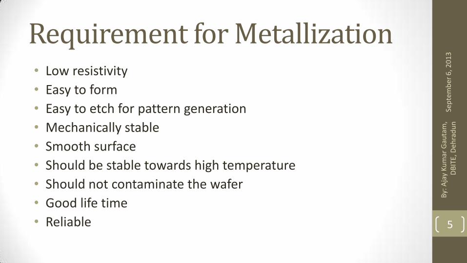
Requirement for Metallization• Low resistivity
• Easy to form
• Easy to etch for pattern generation
• Mechanically stable
• Smooth surface
• Should be stable towards high temperature
• Should not contaminate the wafer
• Good life time
• Reliable
Sep
tem
ber
6, 2
01
3B
y: A
jay
Ku
mar
Gau
tam
, D
BIT
E, D
ehra
du
n
5

Why Aluminium?• The use of aluminium offers the following advantages.
1. It has relatively good conductivity.
2. It is easy to deposit the thin film of aluminium by vacuum evaporation.
3. It has good adherence to the silicon dioxide surface.
4. It has good mechanical bond with silicon.
Sep
tem
ber
6, 2
01
3B
y: A
jay
Ku
mar
Gau
tam
, D
BIT
E, D
ehra
du
n
6
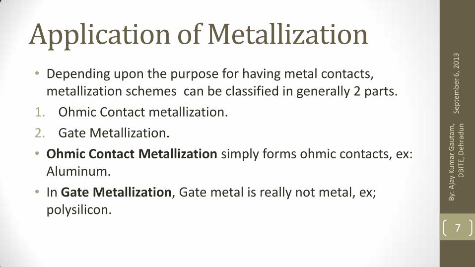
Application of Metallization• Depending upon the purpose for having metal contacts,
metallization schemes can be classified in generally 2 parts.
1. Ohmic Contact metallization.
2. Gate Metallization.
• Ohmic Contact Metallization simply forms ohmic contacts, ex: Aluminum.
• In Gate Metallization, Gate metal is really not metal, ex; polysilicon.
Sep
tem
ber
6, 2
01
3B
y: A
jay
Ku
mar
Gau
tam
, D
BIT
E, D
ehra
du
n
7

Ohmic Contact Metallization•
Sep
tem
ber
6, 2
01
3B
y: A
jay
Ku
mar
Gau
tam
, D
BIT
E, D
ehra
du
n
8

Steps for Metal Deposition• Initially, we have metal in solid form.
• We have form this metal into gas or vapor.
• After getting metal in gaseous form, transport it to the target where we want to deposit the metal.
• Finally, the metal which is in gaseous form, it must be condensed back as a film on the target.
• So, there are 3 steps for deposition of metal.
1. Convert solid metal in gas/vapor.
2. Transport it to the target.
3. Condensation of vapor/gas and growth of the film.
Sep
tem
ber
6, 2
01
3B
y: A
jay
Ku
mar
Gau
tam
, D
BIT
E, D
ehra
du
n
9
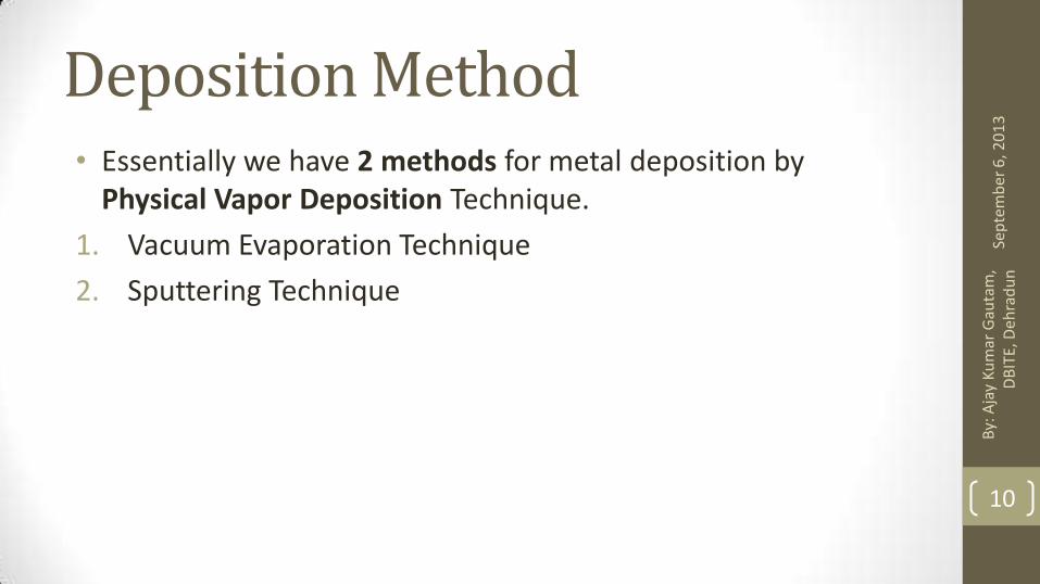
Deposition Method• Essentially we have 2 methods for metal deposition by
Physical Vapor Deposition Technique.
1. Vacuum Evaporation Technique
2. Sputtering Technique
Sep
tem
ber
6, 2
01
3B
y: A
jay
Ku
mar
Gau
tam
, D
BIT
E, D
ehra
du
n
10

1. Vacuum Evaporation Technique
• Initially we have a substrate which is kept at a lower temperature.
• The metal source is placed at a heater.
• Then we heat the metal source, the metal forms the vapor.
• As the substrate is at lower temperature it condenses (Vapor) on the substrate.
• E – Beam Technique is used if the metal has very high melting point.
Sep
tem
ber
6, 2
01
3B
y: A
jay
Ku
mar
Gau
tam
, D
BIT
E, D
ehra
du
n
11

Sep
tem
ber
6, 2
01
3B
y: A
jay
Ku
mar
Gau
tam
, D
BIT
E, D
ehra
du
n
12Fig: Vacuum Evaporation Chamber for metal deposition [S. M. Sze Page 389]

Cond…• Vacuum Evaporation Chamber for metal deposition has shown on
previous slide.• Chamber has gas/air inlet.• We have a combination of pumps.• Roughing pump is used to create the rough vacuum.• High vacuum pump along with cryotrap and force pump is used to
create high vacuum.• Source (metal) is placed inside the chamber.• When we open the inlet valve and roughing valve, the roughing
pump creates the rough vacuum.• After the rough vacuum has been achieved, open the high vacuum
valve.
Sep
tem
ber
6, 2
01
3B
y: A
jay
Ku
mar
Gau
tam
, D
BIT
E, D
ehra
du
n
13

Cond…• Now the substrate is heated slightly.
• And finally metal is evaporated so that metal deposition can take place.
• So, there are basically 4 steps in Vacuum Evaporation technique.
1. Create the rough vacuum
2. Create the high vacuum
3. Heat the substrate
4. Evaporation of metal
Sep
tem
ber
6, 2
01
3B
y: A
jay
Ku
mar
Gau
tam
, D
BIT
E, D
ehra
du
n
14

2. Sputtering Technique• In this technique, we have a big target material.
• Metal source is usually a big disc.
• The target material is bombarded by energetic ions.
• So, Physical Etching takes place.
• So, from the target material some material is pulled out by the force.
• After that the material is condensed on the substrate to form the film of the metal.
• Advantages of this technique is that it has capability of cleaning the substrate prior to metal deposition.
• Disadvantage is that, this process damages the surface of the substrate if the ions have high energy.
Sep
tem
ber
6, 2
01
3B
y: A
jay
Ku
mar
Gau
tam
, D
BIT
E, D
ehra
du
n
15
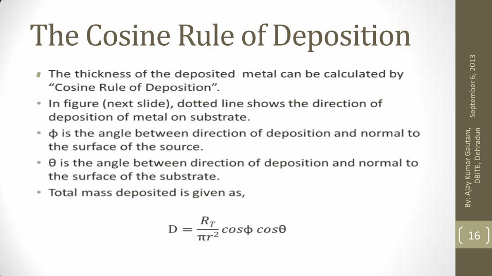
The Cosine Rule of Deposition•
Sep
tem
ber
6, 2
01
3B
y: A
jay
Ku
mar
Gau
tam
, D
BIT
E, D
ehra
du
n
16

Sep
tem
ber
6, 2
01
3B
y: A
jay
Ku
mar
Gau
tam
, D
BIT
E, D
ehra
du
n
17Fig: The Cosine Rule of Deposition
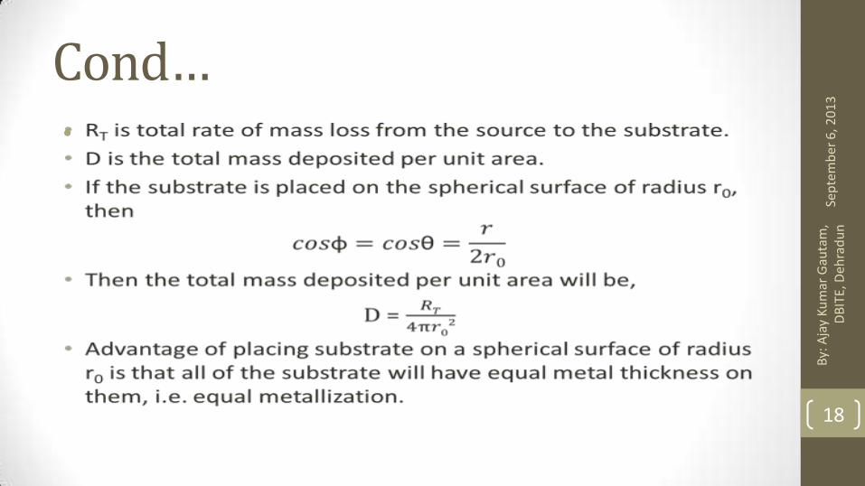
Cond…•
Sep
tem
ber
6, 2
01
3B
y: A
jay
Ku
mar
Gau
tam
, D
BIT
E, D
ehra
du
n
18
Metallization Patterning• When the metallization has been done, the metal film must be
patterned in order to produce required interconnection.
• So we have the following steps for patterning of metal.
1. Lithography
2. Etching
• Now describe these steps in detail.
• These steps are discussed already. So study and describe your self.
Sep
tem
ber
6, 2
01
3B
y: A
jay
Ku
mar
Gau
tam
, D
BIT
E, D
ehra
du
n
19

Problem associated with Metallization
• There are basically 2 problems associated with metallization.
1. Junction spiking
2. Electro-migration
• Now discuss these problems in detail.
Sep
tem
ber
6, 2
01
3B
y: A
jay
Ku
mar
Gau
tam
, D
BIT
E, D
ehra
du
n
20

1. Junction Spiking• Let we have a p-n junction.
• We put metal on p region.
Sep
tem
ber
6, 2
01
3B
y: A
jay
Ku
mar
Gau
tam
, D
BIT
E, D
ehra
du
n
21

Cond…• At 450 0C, Aluminium dissolves 0.5% of Silicon by weight.
• If the contact window is smaller and the junction is shallow, then there is possibility of junction spiking. Se
pte
mb
er 6
, 20
13
By:
Aja
y K
um
ar G
auta
m,
DB
ITE,
Deh
rad
un
22
How to reduce the problem of junction spiking• Now the question is “How to reduce the problem of junction spiking”.
• Initially during metal deposition, don’t deposit the pure aluminium.
• Aluminium must have little bit of silicon mixed.
• So the deposited metal has already some amount of silicon.
• When at 450 0C, when it starts to dissolve 0.5% of Silicon, the silicon is supplied from the Aluminium itself.
• It doesn’t need to take silicon from substrate.
• So, one possibility is that the metal must contain some amount of silicon.
Sep
tem
ber
6, 2
01
3B
y: A
jay
Ku
mar
Gau
tam
, D
BIT
E, D
ehra
du
n
23
Cond…• Usually we have, Al with Si > 1 weight %.
• But there is a small problem.
• As the aluminium is not only used to form contact for p – type silicon, but also used for heavily doped n – type silicon.
• Let we have heavily doped n+ region on which we have to put Al with Si to form the ohmic contact.
• The Aluminium is already having Si, i.e., p – type Silicon in it.
• So, in this case we may again have p – n junction.
• So, for this problem instead of using aluminium with silicon, we first use a novel metal silicide.
• So, first deposit platinum or palladium silicide.
Sep
tem
ber
6, 2
01
3B
y: A
jay
Ku
mar
Gau
tam
, D
BIT
E, D
ehra
du
n
24

Cond…• Now, if we put Aluminium on this silicide, aluminium still keep
eating silicon from this silicide itself.
• So refractory metal barrier is placed on the top of silicide (Tungsten (WSi2)/Titanium(TaSi2)).
• After that deposit aluminium on the metal barrier.
• This is called multilevel contact metallization.
• There are 3 levels
1. Novel metal silicide
2. Refractory metal
3. Metal (Aluminium).
Sep
tem
ber
6, 2
01
3B
y: A
jay
Ku
mar
Gau
tam
, D
BIT
E, D
ehra
du
n
25
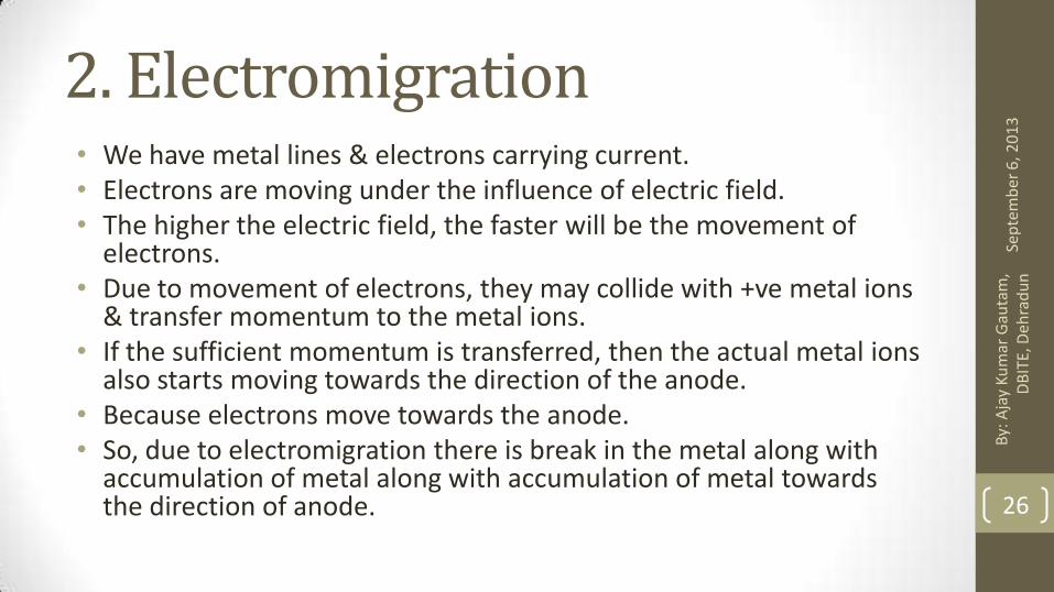
2. Electromigration• We have metal lines & electrons carrying current.• Electrons are moving under the influence of electric field.• The higher the electric field, the faster will be the movement of
electrons.• Due to movement of electrons, they may collide with +ve metal ions
& transfer momentum to the metal ions.• If the sufficient momentum is transferred, then the actual metal ions
also starts moving towards the direction of the anode.• Because electrons move towards the anode.• So, due to electromigration there is break in the metal along with
accumulation of metal along with accumulation of metal towards the direction of anode.
Sep
tem
ber
6, 2
01
3B
y: A
jay
Ku
mar
Gau
tam
, D
BIT
E, D
ehra
du
n
26
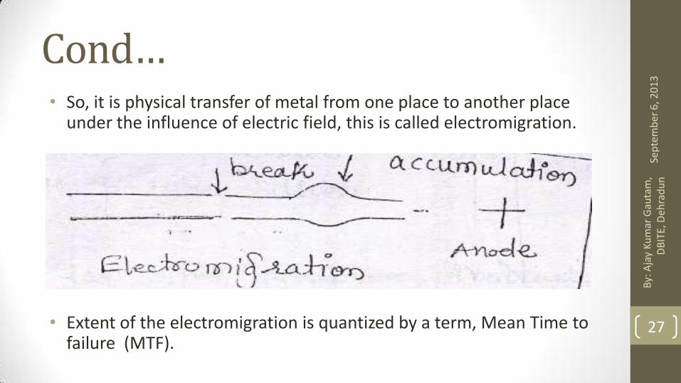
Cond…• So, it is physical transfer of metal from one place to another place
under the influence of electric field, this is called electromigration.
• Extent of the electromigration is quantized by a term, Mean Time to failure (MTF).
Sep
tem
ber
6, 2
01
3B
y: A
jay
Ku
mar
Gau
tam
, D
BIT
E, D
ehra
du
n
27
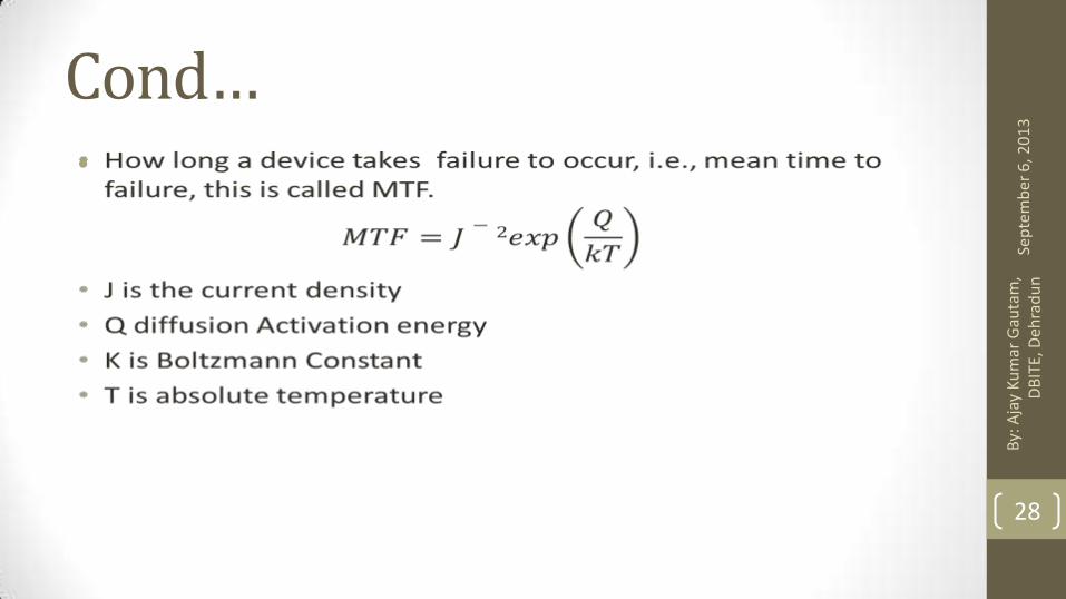
Cond…•
Sep
tem
ber
6, 2
01
3B
y: A
jay
Ku
mar
Gau
tam
, D
BIT
E, D
ehra
du
n
28
How to reduce problem of Electromigration• The metal layer to be deposited is usually polycrystalline.
• Aluminium layer is so polycrystalline layer.
• As, the metal line become narrower, as the line width is decreased. Mean time to failure (MTF) increases.
• It is because of the fact, that when line width decreases, aluminium tends to form a single crystal layer.
• Electromigration can be reduced by using aluminium with copper.
• If its is do so, then Q will be increased & ultimately MTF increases.
Sep
tem
ber
6, 2
01
3B
y: A
jay
Ku
mar
Gau
tam
, D
BIT
E, D
ehra
du
n
29

VLSI PROCESS INTEGRATION
Module 2
Sep
tem
ber
6, 2
01
3B
y: A
jay
Ku
mar
Gau
tam
, D
BIT
E, D
ehra
du
n
30

NMOS IC Technology• The basic n channel circuit consists of NMOS transistors.
• MOS transistors consists of a source, a drain a and a gate region.
• Each transistor is isolated form its neighbor transistors and other devices by a thick field oxide.
• Usually phosphorus doped SiO2, called P – glass is used as insulating layer.
• Under this SiO2 layer, a thin layer of dopant is used, called Chan-stop region.
• The Chan-stop region serves to improve isolation between transistors.
Sep
tem
ber
6, 2
01
3B
y: A
jay
Ku
mar
Gau
tam
, D
BIT
E, D
ehra
du
n
31

Cond…• When +ve charge is applied at the gate, then –ve charge starts
to move from the source to drain.
• Following points will be discussed.
Fabrication process sequence for NMOS
Special Considerations for NMOS ICs
Sep
tem
ber
6, 2
01
3B
y: A
jay
Ku
mar
Gau
tam
, D
BIT
E, D
ehra
du
n
32
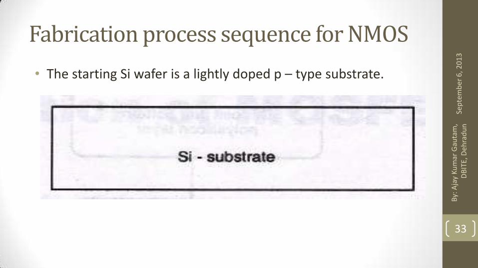
Fabrication process sequence for NMOS
• The starting Si wafer is a lightly doped p – type substrate.
Sep
tem
ber
6, 2
01
3B
y: A
jay
Ku
mar
Gau
tam
, D
BIT
E, D
ehra
du
n
33
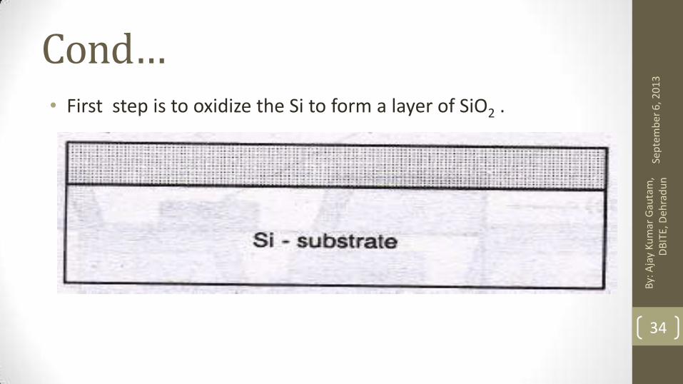
Cond…• First step is to oxidize the Si to form a layer of SiO2 .
Sep
tem
ber
6, 2
01
3B
y: A
jay
Ku
mar
Gau
tam
, D
BIT
E, D
ehra
du
n
34

Cond…• Coat the Si with photoresist.
Sep
tem
ber
6, 2
01
3B
y: A
jay
Ku
mar
Gau
tam
, D
BIT
E, D
ehra
du
n
35

Cond…• Since we have to transfer patterns in order to form source and
drain region, so the next step is lithography.
Sep
tem
ber
6, 2
01
3B
y: A
jay
Ku
mar
Gau
tam
, D
BIT
E, D
ehra
du
n
36

Cond…• Now, the SiO2 regions which are not covered by hardened
photoresist can be etched away either by chemical etching or dry etching. Se
pte
mb
er 6
, 20
13
By:
Aja
y K
um
ar G
auta
m,
DB
ITE,
Deh
rad
un
37

Cond…• The remaining photoresist can be removes by using another
solvent.
Sep
tem
ber
6, 2
01
3B
y: A
jay
Ku
mar
Gau
tam
, D
BIT
E, D
ehra
du
n
38
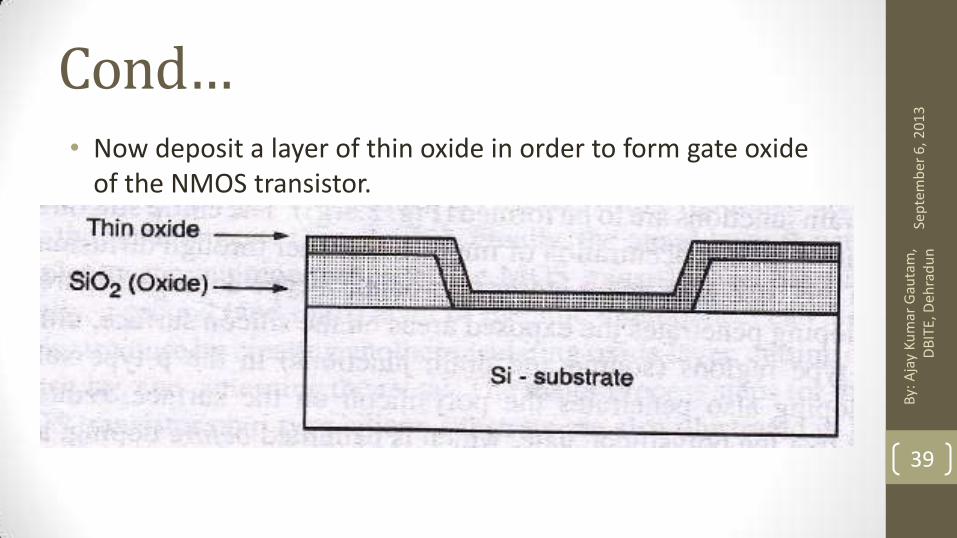
Cond…• Now deposit a layer of thin oxide in order to form gate oxide
of the NMOS transistor.
Sep
tem
ber
6, 2
01
3B
y: A
jay
Ku
mar
Gau
tam
, D
BIT
E, D
ehra
du
n
39
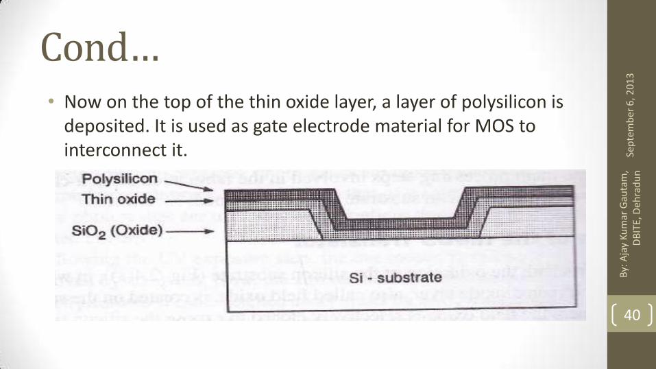
Cond…• Now on the top of the thin oxide layer, a layer of polysilicon is
deposited. It is used as gate electrode material for MOS to interconnect it. Se
pte
mb
er 6
, 20
13
By:
Aja
y K
um
ar G
auta
m,
DB
ITE,
Deh
rad
un
40

Cond…• After deposition of the polysilicon layer, it is patterned and
etched to form the interconnects and the MOS transistor gate.
Sep
tem
ber
6, 2
01
3B
y: A
jay
Ku
mar
Gau
tam
, D
BIT
E, D
ehra
du
n
41

Cond…• The thin oxide not covered by polysilicon is also etched away
so that source and drain junctions may be formed.
Sep
tem
ber
6, 2
01
3B
y: A
jay
Ku
mar
Gau
tam
, D
BIT
E, D
ehra
du
n
42

Cond…• The entire silicon surface is then doped with a high
concentration of impurities either by diffusion or ion implantation. Se
pte
mb
er 6
, 20
13
By:
Aja
y K
um
ar G
auta
m,
DB
ITE,
Deh
rad
un
43
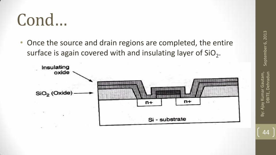
Cond…• Once the source and drain regions are completed, the entire
surface is again covered with and insulating layer of SiO2.
Sep
tem
ber
6, 2
01
3B
y: A
jay
Ku
mar
Gau
tam
, D
BIT
E, D
ehra
du
n
44

Cond…• The insulating oxide is then patterned in order to provide
contact window for drain and source junctions.
Sep
tem
ber
6, 2
01
3B
y: A
jay
Ku
mar
Gau
tam
, D
BIT
E, D
ehra
du
n
45
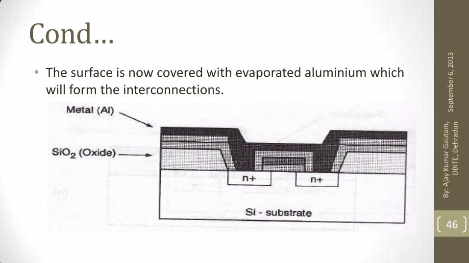
Cond…• The surface is now covered with evaporated aluminium which
will form the interconnections.
Sep
tem
ber
6, 2
01
3B
y: A
jay
Ku
mar
Gau
tam
, D
BIT
E, D
ehra
du
n
46

Cond…• Finally the metal layer is patterned and etched, completing
the interconnections of the MOS transistor on the surface.
Sep
tem
ber
6, 2
01
3B
y: A
jay
Ku
mar
Gau
tam
, D
BIT
E, D
ehra
du
n
47
Cond…• MOS transistors must be electrically isolated from each other
during fabrication.
• Isolation is required to prevent unwanted conduction path between devices.
Sep
tem
ber
6, 2
01
3B
y: A
jay
Ku
mar
Gau
tam
, D
BIT
E, D
ehra
du
n
48

Special Considerations for NMOS ICs
• Following special considerations for NMOS ICs.
A. Starting Material
B. Isolation
C. Channel doping
D. Gate material
E. Source/Drain formation
Sep
tem
ber
6, 2
01
3B
y: A
jay
Ku
mar
Gau
tam
, D
BIT
E, D
ehra
du
n
49

A. Starting Material• Starting material for the fabrication of NMOS is silicon wafer
with <100> orientation.
• <100> orientation is preferred over <111> orientation because it has 10 times lesser interface trap density at the Si – SiO2
interface.
• These trap charges usually create variations in VT.
• For NMOS IC Technology, the Si wafer is lightly doped p – type.
Sep
tem
ber
6, 2
01
3B
y: A
jay
Ku
mar
Gau
tam
, D
BIT
E, D
ehra
du
n
50

B. Isolation• Two transistors are isolated by limiting the conduction of the
parasitic transistor.
• NMOS transistor consists of a polysilicon gate with gate oxide and a Chan-stop region i.e., channel.
• For isolation, the field oxide should be as thick as possible and the Chan-stop as heavily doped as possible.
Sep
tem
ber
6, 2
01
3B
y: A
jay
Ku
mar
Gau
tam
, D
BIT
E, D
ehra
du
n
51Fig: MOSFET Isolation[S M Sze 476]

C. Channel Doping• The channel doping level of the silicon in the channel region of the
NMOS determines the threshold voltage of the device along with the gate oxide thickness.
• So for desired threshold voltage (VT) the channel doping must be chosen by accurate gate material and gate oxide.
• The channel doping must not be too high or too low.• If the channel doping is too high, it can cause a reduction of carrier
mobility at the surface.• If the channel doping is too low, then drain electric field will punch
through the source.• The channel doping depends upon drain junction depth and channel
depth.
Sep
tem
ber
6, 2
01
3B
y: A
jay
Ku
mar
Gau
tam
, D
BIT
E, D
ehra
du
n
52

Sep
tem
ber
6, 2
01
3B
y: A
jay
Ku
mar
Gau
tam
, D
BIT
E, D
ehra
du
n
53Fig: Punch Through situation [S M Sze 478]

Cond…• For large drain bias voltage, the depletion region surrounding
the drain can extend toward the source.
• Also the two depletion region can merge.
• This is called “punch through”.
• The gate voltage loses its control upon the drain current.
• So, in order to reduce the Punch Through Situation, implant boron sufficiently deep into the channel region so that substrate doping can be raised.
• The implantation of boron raise the VT.
• The implantation of Arsenic or Phosphorus reduce the VT.
Sep
tem
ber
6, 2
01
3B
y: A
jay
Ku
mar
Gau
tam
, D
BIT
E, D
ehra
du
n
54

D. Gate Material• For the gate interconnections usually heavily doped n type
polysilicon is used.
• To reduce the resistance of the gate material, refractory metal silicide are used on the top of polysilicon gate.
• Silicide is formed by depositing the metal layer on exposed silicon.
• This approach is called “Polycide”.
Sep
tem
ber
6, 2
01
3B
y: A
jay
Ku
mar
Gau
tam
, D
BIT
E, D
ehra
du
n
55
E. Source/Drain formation• The resistance of the n+ source/drain region of the NMOS transistor
should be low.
• For VLSI applications, the junctions should be shallow because of the small dimensions.
• Arsenic is used as the dopant for the source/drain because it has high solubility and low diffusion rate.
• The resistance of the source/drain regions can be reduced by using a refractory metal silicide.
• This process is called “Salicide”.
• So, use of silicide is that it reduces the resistance of source/drain regions.
Sep
tem
ber
6, 2
01
3B
y: A
jay
Ku
mar
Gau
tam
, D
BIT
E, D
ehra
du
n
56
Sep
tem
ber
6, 2
01
3B
y: A
jay
Ku
mar
Gau
tam
, D
BIT
E, D
ehra
du
n
57
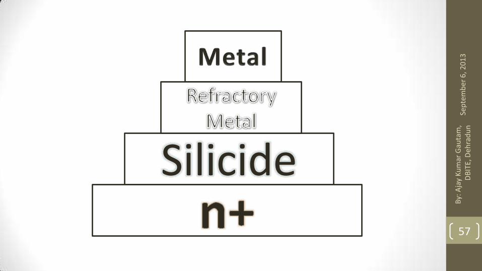
Silicide

Cond…• In the smaller devices when device dimensions are reduced
but the VSS (Supply Voltage) is maintained constant (5 V), then the electric field in the silicon substrate increases.
• This effect is called “Hot Electron Problem”.
• Due to hot electron problem, threshold voltage increases & large amount of electrons may inject into oxide.
• The “Hot Electron Problem” can be reduced by minimizing the electric field at the drain region.
• There are 2 techniques to reduce this problem.
Sep
tem
ber
6, 2
01
3B
y: A
jay
Ku
mar
Gau
tam
, D
BIT
E, D
ehra
du
n
58

Cond…• First technique is to implant the lightly doped n- regions into
source/drain regions.
• Second technique is to implant phosphorus and arsenic into the drain/source regions as shown in figure.
• The electric field in the drain region is reduced for both of these cases.
Sep
tem
ber
6, 2
01
3B
y: A
jay
Ku
mar
Gau
tam
, D
BIT
E, D
ehra
du
n
59

Fig:
Sep
tem
ber
6, 2
01
3B
y: A
jay
Ku
mar
Gau
tam
, D
BIT
E, D
ehra
du
n
60
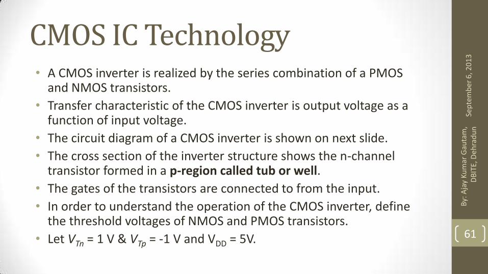
CMOS IC Technology• A CMOS inverter is realized by the series combination of a PMOS
and NMOS transistors.
• Transfer characteristic of the CMOS inverter is output voltage as a function of input voltage.
• The circuit diagram of a CMOS inverter is shown on next slide.
• The cross section of the inverter structure shows the n-channel transistor formed in a p-region called tub or well.
• The gates of the transistors are connected to from the input.
• In order to understand the operation of the CMOS inverter, define the threshold voltages of NMOS and PMOS transistors.
• Let VTn = 1 V & VTp = -1 V and VDD = 5V.
Sep
tem
ber
6, 2
01
3B
y: A
jay
Ku
mar
Gau
tam
, D
BIT
E, D
ehra
du
n
61

Symbol, Diagram and VTC
Sep
tem
ber
6, 2
01
3
62
By:
Aja
y K
um
ar G
auta
m,
DB
ITE,
Deh
rad
un
CMOS Inverter
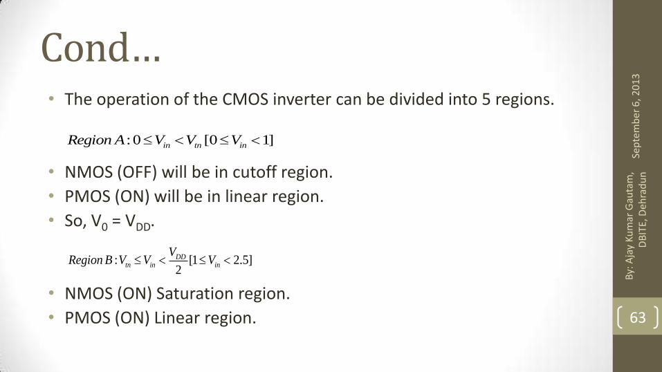
Cond…• The operation of the CMOS inverter can be divided into 5 regions.
• NMOS (OFF) will be in cutoff region.
• PMOS (ON) will be in linear region.
• So, V0 = VDD.
• NMOS (ON) Saturation region.
• PMOS (ON) Linear region.
Sep
tem
ber
6, 2
01
3B
y: A
jay
Ku
mar
Gau
tam
, D
BIT
E, D
ehra
du
n
63
:0 [0 1]in tn inRegion A V V V
: [1 2.5]2
DDtn in in
VRegion B V V V

Cond…
• NMOS (ON) Saturation region.
• PMOS (ON) Saturation region.
• PMOS (ON) saturation region.
• NMOS (ON) Linear region.
Sep
tem
ber
6, 2
01
3B
y: A
jay
Ku
mar
Gau
tam
, D
BIT
E, D
ehra
du
n
64
: [ 2.5]2
DDin in
VRegionC V V
: [2.5 3.5]2 2
DD DDin tp in
V VRegion D V V V

Cond…
• PMOS (OFF) cutoff region.
• NMOS (ON) linear region.
Sep
tem
ber
6, 2
01
3B
y: A
jay
Ku
mar
Gau
tam
, D
BIT
E, D
ehra
du
n
65
: [3.5 5]2
DDtp in DD in
VRegion E V V V V

N Well (Well) CMOS IC
S. M. Sze
Sep
tem
ber
6, 2
01
3
66
By:
Aja
y K
um
ar G
auta
m,
DB
ITE,
Deh
rad
un

P Tub (Well) CMOS IC
S. M. Sze
Sep
tem
ber
6, 2
01
3
67
By:
Aja
y K
um
ar G
auta
m,
DB
ITE,
Deh
rad
un

Twin Tub CMOS IC
S. M. Sze
Sep
tem
ber
6, 2
01
3
68
By:
Aja
y K
um
ar G
auta
m,
DB
ITE,
Deh
rad
un

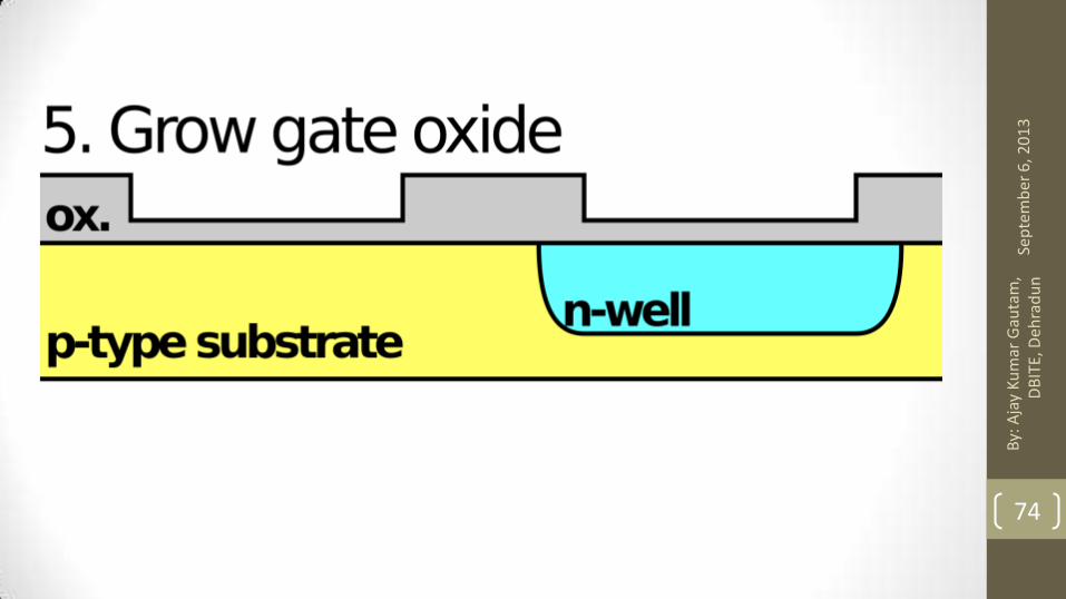
Fabrication Process Sequence for N Well CMOS
Sep
tem
ber
6, 2
01
3B
y: A
jay
Ku
mar
Gau
tam
, D
BIT
E, D
ehra
du
n
69
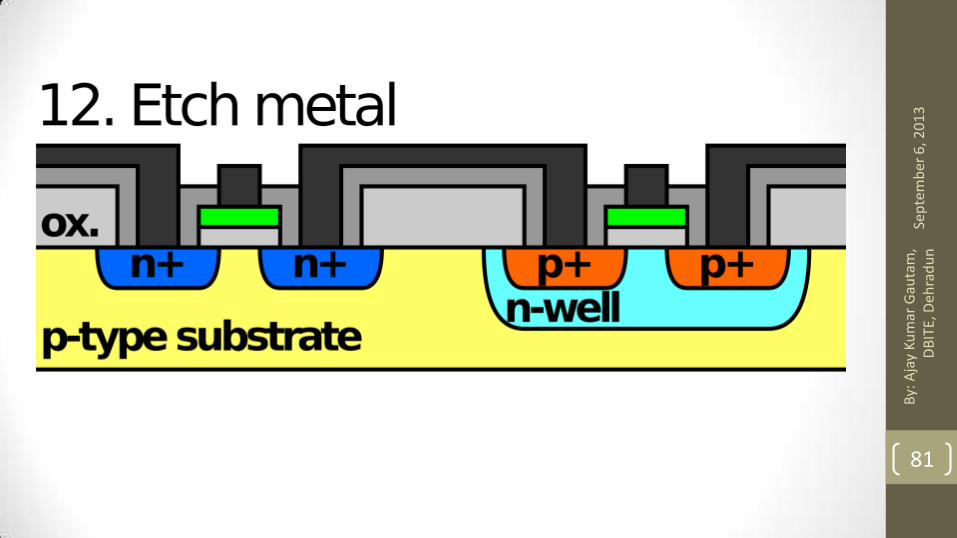
Oxidation
Etch for PMOS
Diffuse N Well
Etch for NMOS
Grow Gate Oxide
Deposit Polysilicon
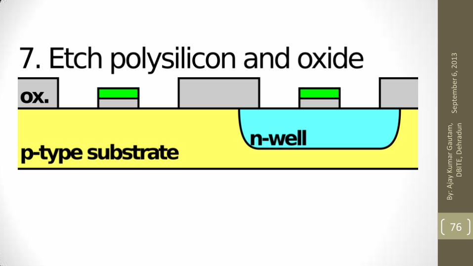
Etch Polysilicon
& Oxide
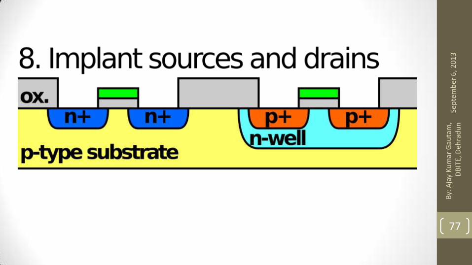
Implant Sources &
Drains
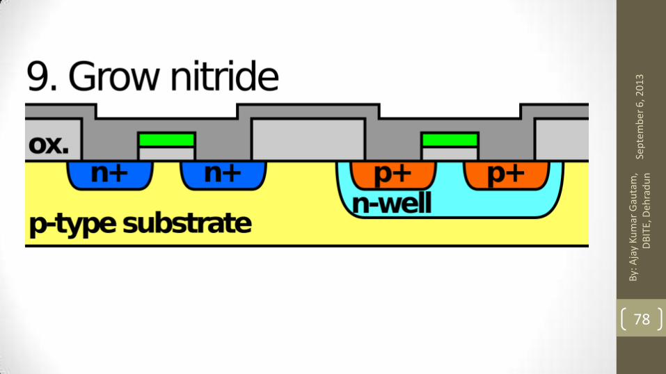
Grow Nitride
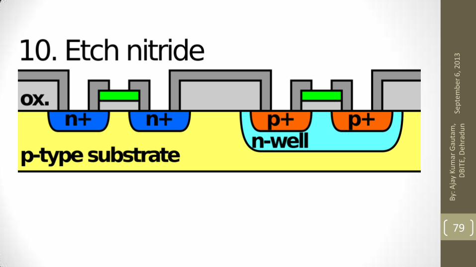
Etch Nitride
Deposit Metal
Etch Metal

Sep
tem
ber
6, 2
01
3B
y: A
jay
Ku
mar
Gau
tam
, D
BIT
E, D
ehra
du
n
70

Sep
tem
ber
6, 2
01
3B
y: A
jay
Ku
mar
Gau
tam
, D
BIT
E, D
ehra
du
n
71

Sep
tem
ber
6, 2
01
3B
y: A
jay
Ku
mar
Gau
tam
, D
BIT
E, D
ehra
du
n
72

Sep
tem
ber
6, 2
01
3B
y: A
jay
Ku
mar
Gau
tam
, D
BIT
E, D
ehra
du
n
73
Sep
tem
ber
6, 2
01
3B
y: A
jay
Ku
mar
Gau
tam
, D
BIT
E, D
ehra
du
n
74

Sep
tem
ber
6, 2
01
3B
y: A
jay
Ku
mar
Gau
tam
, D
BIT
E, D
ehra
du
n
75
Sep
tem
ber
6, 2
01
3B
y: A
jay
Ku
mar
Gau
tam
, D
BIT
E, D
ehra
du
n
76
Sep
tem
ber
6, 2
01
3B
y: A
jay
Ku
mar
Gau
tam
, D
BIT
E, D
ehra
du
n
77
Sep
tem
ber
6, 2
01
3B
y: A
jay
Ku
mar
Gau
tam
, D
BIT
E, D
ehra
du
n
78
Sep
tem
ber
6, 2
01
3B
y: A
jay
Ku
mar
Gau
tam
, D
BIT
E, D
ehra
du
n
79

Sep
tem
ber
6, 2
01
3B
y: A
jay
Ku
mar
Gau
tam
, D
BIT
E, D
ehra
du
n
80
Sep
tem
ber
6, 2
01
3B
y: A
jay
Ku
mar
Gau
tam
, D
BIT
E, D
ehra
du
n
81

Special Considerations for CMOS ICs
A. Isolation
B. Gate Material and Threshold Adjustment
Sep
tem
ber
6, 2
01
3B
y: A
jay
Ku
mar
Gau
tam
, D
BIT
E, D
ehra
du
n
82

A. Isolation
• Isolation between two adjacent transistors in CMOS circuits is necessary.
• A parasitic n – channel transistor exists between the n+ source and adjacent n tub.
• Similar case exists for p tub.
• These parasitic transistors causes variations in the original transistors.
• So it is necessary to isolate the n channel and p channel transistors in order to avoid the undesirable parasitic currents between the transistors..
Sep
tem
ber
6, 2
01
3B
y: A
jay
Ku
mar
Gau
tam
, D
BIT
E, D
ehra
du
n
83

Fig: Isolation of n and p channel transistors
S m sze page 488
Sep
tem
ber
6, 2
01
3B
y: A
jay
Ku
mar
Gau
tam
, D
BIT
E, D
ehra
du
n
84

B. Gate Material and Threshold Adjustment
• Gate material and channel doping level are responsible for threshold voltage for the transistors.
• The threshold voltage should be as low as possible.
• Usually n type polysilicon with silicide layer is used to decrease the sheet resistance as discussed in NMOS technology.
• The threshold voltage for a MOS device is given by the equation:
Sep
tem
ber
6, 2
01
3B
y: A
jay
Ku
mar
Gau
tam
, D
BIT
E, D
ehra
du
n
852
f BT ms B
ox ox
Q QV
C C

Cond…
Sep
tem
ber
6, 2
01
3B
y: A
jay
Ku
mar
Gau
tam
, D
BIT
E, D
ehra
du
n
86
in
tan
ms
f
B
B
ox
metal silicon work functiondifferenceof the gatematerial
Q Charge the gateoxide
substrate fermi potential
Q Depletion regionChargeinthe substrate
C capaci ceof the gateoxide

Cond…• Cox is inversely proportional to the gate oxide thickness.
• QB is proportional to the square root of the channel doping.
• These 2 parameters can be used to adjust the threshold voltages of the transistor.
• The threshold voltage VTn is easily adjusted from 0 to +1 V with a substrate doping range of 1015 to 1017 cm-3.
• The threshold voltage VTp cannot be adjusted for ! VTp! Less than 0.7 V by reducing the p channel substrate doping.
Sep
tem
ber
6, 2
01
3B
y: A
jay
Ku
mar
Gau
tam
, D
BIT
E, D
ehra
du
n
87

Cond…• The p channel threshold voltage VTp can be adjusted by
implant a shallow boron layer into the channel region.
• The boron shifts the threshold voltages towards more positive values.
Sep
tem
ber
6, 2
01
3B
y: A
jay
Ku
mar
Gau
tam
, D
BIT
E, D
ehra
du
n
88
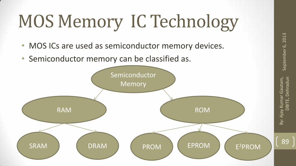
MOS Memory IC Technology• MOS ICs are used as semiconductor memory devices.
• Semiconductor memory can be classified as.
Sep
tem
ber
6, 2
01
3B
y: A
jay
Ku
mar
Gau
tam
, D
BIT
E, D
ehra
du
n
89
Semiconductor Memory
RAM ROM
SRAM DRAM E2PROMEPROMPROM

Cond…• Semiconductor memory is generally classified according to the
data storage and data access.
• RAM permits modification of data bits (writing) stored in the memory array, as well as retrieval (reading) on demand.
• So, RAM is also called as R/W memory.
• THE DRAM consists of a capacitor to store binary information.
• So, because of the capacitor, cell data must be read and rewritten periodically (refresh operation) even when the memory array are not accessed.
Sep
tem
ber
6, 2
01
3B
y: A
jay
Ku
mar
Gau
tam
, D
BIT
E, D
ehra
du
n
90
Cond…• On the other hand, SRAM cell doesn’t consists of capacitor, so
cell data is kept as long as power is turned on & refresh operation not required.
• Due to advantage of low cost and high packing density DRAM is widely used for the main memory in personal computer.
• SRAM cell is mainly used for the cache memory in microprocessor & hand held devices due to high speed and low power consumption.
Sep
tem
ber
6, 2
01
3B
y: A
jay
Ku
mar
Gau
tam
, D
BIT
E, D
ehra
du
n
91
Cond…• ROM are permanently data storage memory devices, there is
no way of modifying the data.
• PROM are ROM that can be programmed externally after manufacturing.
• If the data stored can also be erased by some means then the circuit is an erasable PROM or EPROM.
• When high electrical voltage is used to erase data, it is called E2PROM.
Sep
tem
ber
6, 2
01
3B
y: A
jay
Ku
mar
Gau
tam
, D
BIT
E, D
ehra
du
n
92

A. Dynamic Memory• MOS with capacitor is used to store single bit of information.
• Simplest DRAM cell has a single transistor and a capacitor.
• Due to simplicity, DRAM has maximized density of the circuit.
• It needs periodic refreshment.
• The simplest example of DRAM cell is shown in figure.
• It consists of a single NMOS transistor and a storage capacitor.
• The GATE of the NMOS transistor is connected to a ROW Select or Word Line.
Sep
tem
ber
6, 2
01
3B
y: A
jay
Ku
mar
Gau
tam
, D
BIT
E, D
ehra
du
n
93

Simplest DRAM Cell
S M Sze
Sep
tem
ber
6, 2
01
3
94
By:
Aja
y K
um
ar G
auta
m,
DB
ITE,
Deh
rad
un
Cond…• The source of the NMOS is connected to the Bit Line.
• Since NMOS works as a switch, so when both source & Gate are at high, the transistor is on and the charge flow to the capacitor.
• If initially the capacitor had no charge (stored 0) then charge flows into the capacitor.
• If initially the capacitor had charge (stored 1) then very little charge flows into the capacitor.
Sep
tem
ber
6, 2
01
3B
y: A
jay
Ku
mar
Gau
tam
, D
BIT
E, D
ehra
du
n
95
Cond…• To read the individual bit, the “sensing circuit” measures the
amount of charge that flows into the capacitor and determines whether it is “0” or “1”.
• The capacitor is then refreshed by either fully charging it or completely discharging it, depending on which state it was in initially.
• So, if the capacitor is fully charged, then sensing circuit measures it “1”.
• If the capacitor doesn’t have charge then “0” will be measured.
Sep
tem
ber
6, 2
01
3B
y: A
jay
Ku
mar
Gau
tam
, D
BIT
E, D
ehra
du
n
96
Cond…• So, for new storage capacitor need refreshment, i.e., it should
be discharged, if it is fully charged.
• The capacitance of the capacitor needs to be as high as possible to give as high signal as possible to the sensing circuitry.
• The bit line capacitance and resistance should be small to improve the performance of the cell.
Sep
tem
ber
6, 2
01
3B
y: A
jay
Ku
mar
Gau
tam
, D
BIT
E, D
ehra
du
n
97

Cond…• The charge stored on a the capacitor is given by:
Sep
tem
ber
6, 2
01
3B
y: A
jay
Ku
mar
Gau
tam
, D
BIT
E, D
ehra
du
n
98
s s s
AQ V AE
d
0
0 2
12
3.9
8.854 10 /
s s s
r
r
s
s
AQ V AE
d
dielectric permitivity
for SiO
x F m
E electric field across thedielectric
d dielectric thickness
V voltageacross thecapacitor

Cond…• For higher packing density cell size should be small and area of
the capacitor should be small.
• So, to increase the charge stored Qs by either by increasing the Es or ε.
• The electric field Es can be increased by decreasing thickness of dielectric (SiO2).
• However, if the oxide thickness is too low, the electric field will be too high and the capacitor may short.
• The electric field may also be increased by increasing net +ve charge directly under the oxide.
Sep
tem
ber
6, 2
01
3B
y: A
jay
Ku
mar
Gau
tam
, D
BIT
E, D
ehra
du
n
99
Cond…• So, to increase this charge, implant both boron and shallow
arsenic under the capacitor.
• This increases the charge storage capacity. It is called a High –Capacity (Hi - C) RAM Cell.
Sep
tem
ber
6, 2
01
3B
y: A
jay
Ku
mar
Gau
tam
, D
BIT
E, D
ehra
du
n
100
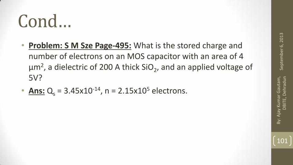
Cond…• Problem: S M Sze Page-495: What is the stored charge and
number of electrons on an MOS capacitor with an area of 4 µm2, a dielectric of 200 A thick SiO2, and an applied voltage of 5V?
• Ans: Qs = 3.45x10⁻¹⁴, n = 2.15x10⁵ electrons.
Sep
tem
ber
6, 2
01
3B
y: A
jay
Ku
mar
Gau
tam
, D
BIT
E, D
ehra
du
n
101
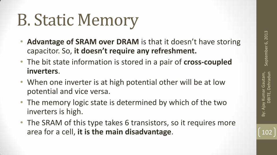
B. Static Memory• Advantage of SRAM over DRAM is that it doesn’t have storing
capacitor. So, it doesn’t require any refreshment.
• The bit state information is stored in a pair of cross-coupled inverters.
• When one inverter is at high potential other will be at low potential and vice versa.
• The memory logic state is determined by which of the two inverters is high.
• The SRAM of this type takes 6 transistors, so it requires more area for a cell, it is the main disadvantage.
Sep
tem
ber
6, 2
01
3B
y: A
jay
Ku
mar
Gau
tam
, D
BIT
E, D
ehra
du
n
102

Cond…• The NMOS SRAM cell is shown in figure.
• Transistors T1 to T4 are cross coupled inverter pair.
• T5 & T6 are the access transistors that transmit the signal into and out of the cell, when both the word line and bit line are simultaneously activated.
• Transistors T1 & T2 works as load for enhancement mode transistors T3 & T4.
• To minimize the cell area, polysilicon is directly connected to the silicon diffused region.
Sep
tem
ber
6, 2
01
3B
y: A
jay
Ku
mar
Gau
tam
, D
BIT
E, D
ehra
du
n
103

Cond…• The transistors are depletion type and as they are used here
only as load so they can be replaced as high value resistor.
• To reduce the cell area, resistors are made up of polysilicon.
• SRAM CELL can also be fabricated using 2 coupled CMOS inverters.
• It requires more area but the power consumption is low.
• In order to improve the packing density, the transistors are stacked on the top of other transistors.
Sep
tem
ber
6, 2
01
3B
y: A
jay
Ku
mar
Gau
tam
, D
BIT
E, D
ehra
du
n
104

Figure: SRAM Cell
cross-coupled CMOS inverters coupled CMOS inverters
Sep
tem
ber
6, 2
01
3B
y: A
jay
Ku
mar
Gau
tam
, D
BIT
E, D
ehra
du
n
105

Fig: Stacked Structure showing common gate
S M Sze
Sep
tem
ber
6, 2
01
3
106
By:
Aja
y K
um
ar G
auta
m,
DB
ITE,
Deh
rad
un
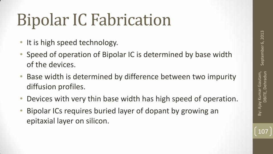
Bipolar IC Fabrication• It is high speed technology.
• Speed of operation of Bipolar IC is determined by base width of the devices.
• Base width is determined by difference between two impurity diffusion profiles.
• Devices with very thin base width has high speed of operation.
• Bipolar ICs requires buried layer of dopant by growing an epitaxial layer on silicon.
Sep
tem
ber
6, 2
01
3B
y: A
jay
Ku
mar
Gau
tam
, D
BIT
E, D
ehra
du
n
107

Fabrication Process Sequence for Bipolar IC
Sep
tem
ber
6, 2
01
3B
y: A
jay
Ku
mar
Gau
tam
, D
BIT
E, D
ehra
du
n
108

Special Considerations for Bipolar ICs
A. Buried layer and epitaxial layer
B. Base formation
C. Emitter formation Sep
tem
ber
6, 2
01
3B
y: A
jay
Ku
mar
Gau
tam
, D
BIT
E, D
ehra
du
n
109
A. Buried layer and epitaxial layer
Sep
tem
ber
6, 2
01
3B
y: A
jay
Ku
mar
Gau
tam
, D
BIT
E, D
ehra
du
n
110

B. Base formation
Sep
tem
ber
6, 2
01
3B
y: A
jay
Ku
mar
Gau
tam
, D
BIT
E, D
ehra
du
n
111
C. Emitter formation
Sep
tem
ber
6, 2
01
3B
y: A
jay
Ku
mar
Gau
tam
, D
BIT
E, D
ehra
du
n
112
Review Questions1. How the thickness of deposited film is measured?
2. Why Metallization is required? What advantages and applications it provide the ICs?
3. What do you mean by sputtering? How it is used in etching and metallization? Describe various advantages and problems with sputtering?
4. Explain the metallization and also describe the problems associated with this process. Explain sputtering method of metallization.
Sep
tem
ber
6, 2
01
3B
y: A
jay
Ku
mar
Gau
tam
, D
BIT
E, D
ehra
du
n
113
Review Questions5. What are the limitations of pure aluminum metallization for
sub-micron level devices?
6. Describe DRAM and SRAM semiconductor memories.
7. With neat diagram explain fabrication process sequence for NMOS IC technology.
8. Why <100> orientation is preferred over <111> orientation for starting material in NMOS/CMOS IC fabrication.
9. What is the “hot electron problem” in NMOS IC? How it can be minimized?
Sep
tem
ber
6, 2
01
3B
y: A
jay
Ku
mar
Gau
tam
, D
BIT
E, D
ehra
du
n
114

Review Questions10. Explain CMOS inverter Voltage transfer characteristic with a
neat diagram. Explain fabrication process for n-tub CMOS IC.
12. Give the various fabrication steps of CMOS transistor using n well technique with diagram and brief explanation.
13. What are the stored charge and the number of electrons on an MOS capacitor with an area of 4 , a dielectric of 200 thick SiO2, and an applied voltage of 5V?
14. Describe various effects if the channel doping is either too low or too high in NMOS IC technology.
Sep
tem
ber
6, 2
01
3B
y: A
jay
Ku
mar
Gau
tam
, D
BIT
E, D
ehra
du
n
115

Review Questions15. Discuss various CMOS structures and describe p tub, n tub
and twin tub structures.
Sep
tem
ber
6, 2
01
3B
y: A
jay
Ku
mar
Gau
tam
, D
BIT
E, D
ehra
du
n
116
References1. S.M. SZE/ VLSI Technology / M Hill. 2009/2nd Edition
2. S. K. Gandhi/VLSI Fabrication Principles/Wiley/2nd edition
3. S.A. Campbell / The Science and Engineering of Microelectronic Fabrication / Oxford 2008/2nd edition
4. Sedra & Smith/ Microelectronic Circuits 2004/Oxford/5th edition
5. James D. Plummer/ Silicon VLSI Technology: Fundamentals, Practice, and Modeling/Pearson/2nded
6. Mr. Rajesh Agarwal/VLSI Technology and Design/Technical Publications/1st Ed./
7. Joseph J. Carr/Linear Integrated Circuits/Newness Press/1st Ed
Sep
tem
ber
6, 2
01
3B
y: A
jay
Ku
mar
Gau
tam
, D
BIT
E, D
ehra
du
n
117