VLSI DESIGN(Unit-2)
73
Basic Circuit Concepts: Capacitance, resistance estimations- Sheet Resistance R s, MOSDivice Capacitances, routing Capacitance, Analytic Inverter Delays, Driving large Capacitive Loads, Fan-in and fan-out. VLSI Circuit Design Processes: VLSI Design Flow, MOS Layers, Stick Diagrams, Design Rules and Layout, 2μm CMOS Design rules for wires, Contacts and Transistors Layout Diagrams for NMOS and CMOS Inverters and Gates, Scaling of MOS circuits, Limitations of Scaling UNIT-II VLSI DESIGN(Unit-2) RCEW, Pasupula (V), Nandikotkur Road, Near Venkayapalli, KURNOOL
Transcript of VLSI DESIGN(Unit-2)

Basic Circuit Concepts: Capacitance, resistance estimations- Sheet
Resistance Rs, MOSDivice Capacitances, routing Capacitance, Analytic
Inverter Delays, Driving large Capacitive Loads, Fan-in and fan-out.
VLSI Circuit Design Processes: VLSI Design Flow, MOS Layers, Stick Diagrams, Design Rules and Layout, 2µm CMOS Design rules for wires, Contacts and Transistors Layout Diagrams for NMOS and CMOS Inverters and Gates, Scaling of MOS circuits, Limitations of Scaling
UNIT-II
VLSI DESIGN(Unit-2)
RCEW, Pasupula (V), Nandikotkur Road, Near Venkayapalli,
KURNOOL

SHEET RESISTANCE Rs
Consider a uniform slab of conducting material of resistivity ρ, of width W,
thickness t, and
length between faces L. The arrangement is shown in Figure
FIGURE Sheet resistance model .
Q)Define Sheet resistance of the MOS device.

With reference to Figure , consider the resistance RAB between
two opposite faces.

For the MOS processes considered here, typical values of sheet resistance are
given in Table

SHEET RESISTANCE CONCEPT.APPLIED·TO-MOS TRANSISTORSAND INVERTERS
FIGURE Resistance calculation for transistor channels

FIGURE Inverter resistance calculation.

AREA CAPACITANCES OF LAYERS
For any layer, knowing the dielectric (silicon dioxide) thickness, we can calculate area
capacitance as follows:

TABLE Typical area capacitance values for MOS circuits
Capacitance

STANDARD UNIT OF CAPACITANCE □ CG
The unit is denoted □Cg and is defined the gate-to-channel capacitance of a
MOS transistor having W = L = feature size, that is, a 'standard' or 'feature size' square as
in Figure

SOME AREA CAPACITANCE CALCULATIONS
Consider the area defined in Figure First, we must calculate the area relative to that
of a standard gate.
FIGURE Simple area for capacitance calculation

Calculations of area capacitance values associated with structures occupying
more than
one layer, as in Figure are equally straightforward
FIGURE Capacitance calculation (multilayer


THE DELAY UNIT
We have developed the concept of sheet resistance Rs and standard gate capacitance unit
□ Cg If we consider the case of one standard (feature size square) gate area capacitance
being charged through one feature size square of n channel resistance (that is, through Rs for
an nMOS pass transistor channel), as in Figure we have:
FIGURE Model for derivation of.


INVERTER DELAYS
Consider the basic 4: 1 ratio nMOS inverter. In order to achieve the 4:1 Zp.u. to Zp.d.
ratio, Rp.u. will be 4 Rp.d. and if Rp.d. is contributed by the minimum size transistor
then, clearly, the resistance value associated with Rp.u. is
Rp.u. = 4RS = 40 kQ Meanwhile, the Rp.d. value is 1Rs = 10 kQ so that the delay
associated with the inverter will depend on whether it is being turned on or off.

FIGURE nMOS Inverter pair delay.

However, a single 4: 1 inverter exhibits undesirable asymmetric delays since the
delay in turning on is, for example,τ, while the corresponding delay in turning
off is 4τ. Quite obviously, the asymmetry is worse when considering an. inverter
with an 8:1 ratio
.
FIGURE Minimum size CMOS Inverter pair delay

A More Formal Estimation of CMOS Inverter Delay
A CMOS inverter, in general, either charges or discharges a capacitive load CL and rise-time τr
or fall-time τf 'can be estimated from the following simple analysis
FIGURE Rise-time model


Fall-time estimation
Similar reasoning can be applied to the discharge of CL through the n-transistor. The circuit
model in this case is given as Figure
FIGURE Fall-time model
Making similar assumptions we may write for fall-time:

Summary of CMOS rise and fall factors

DKMNG LARGE CAPACITIVE LOADS
The problem of driving comparatively large capacitive loads arises when signals must be
propagated from the chip to off chip destinations . . Generally, typical off chip capacitances
may be several orders higher than on chip □Cg values. For example, if the off chip load is
denoted CL then
Clearly capacitances of this order must be driven through low resistances, otherwise
excessively long delays will occur.
Cascaded Inverters as Drivers
FIGURE Driving large capacitive loads

Inverters intended to drive large capacitive loads must therefore present low pull-up and
pull-down resistance
Obviously, for MOS circuits, low resistance values for Zp.d. and Zp.u. imply low L: W
ratios; in other words, channels must be made very wide to reduce resistance value and, in
consequence, an inverter to meet this need occupies a large area. Moreover, because of the
large L: W ratio and since length L cannot be reduced below the minimum feature size, the
gate region area L x W becomes significant and a comparatively large capacitance is presented
at the input, which in tum slows down the rates of change of voltage which can take place
at the input.
The remedy is to use N cascaded inverters, each one of which is larger than the preceding
stage by a width factor f as shown in Figure

Clearly, as the width factor increases, so the capacitive load presented at the inverter
input increases, and the area occupied increases also. Equally clearly, the rate at which the
width increases (that is, the value of.f) will influence the number N of stages which must
be
cascaded to drive a particular value of CL. Thus, an optimum solution must be sought as
follows (


Pair delay or total dealy (td) )=2.5Nfτ
Where N=2
216 4Nf
4f
(td) )=2.5Nfτ
td=2.5X2X4Xτ=20τ
1616
g
g
C
C

MOS design is aimed at turning a specification into masks for processing silicon to meet the
specification. We have seen that MOS circuits are formed on four basic layers-n-diffusion,
p-diffusiqn, polysilicon, and metal, which are isolated from one another by thick or thin
(thinox) silicon dioxide insulating layers
MOS LAYERS
The thin oxide (thinox) mask region includes
.n-diffusion, p-diffusion, and transistor channels
Polysilicon and thinox regions interact so
that a transistor is formed where they cross one another. In some processes, there may
be a
second metal layer and also, in some processes, a second polysilicon layer. Layers may
deliberatelY joined together where contacts are formed.

STICK DIAGRAMS
Stick diagrams may be used to convey layer information through the use of a color codefor
example, in the case of nMOS design, green for n-diffusion, red for polysilicon, blue for
metal, yellow for implant, and black for contact areas.

FIGURE :Encodings for a simple metal nMOS process


Encodings for a double metal CMOS p-well process


nMOS Design Style
In order to start with a relatively simple process, we will consider single metal, single
polysilicon nMOS technology
A rational approach to stick diagram layout is readily adopted for such nMOS circuits
and the approach recommended here is both easy to use and to tum into a mask layout. The
layout of nMOS involves:
• n-diffusion [n-diff.] and other thinoxide regions [thinox] (green);
• polysilicon I [poly.]-since there is only one polysilicon layer here (red);
• metal I [metal]-since we use only one metal layer here (blue);
• implant (yellow);
• contacts (black or brown [buried]).
A transistor is formed wherever poly. crosses n-diff. (red over green) and all diffusion
wires (interconnections) are n-type (green).

When starting a layout, the first step normally taken is to draw the metal (blue) Vdd
and GND rails in parallel allowing enough space between them for the other circuit elements
which will be required.
Next, thinox (green) paths may be drawn between the rails for
inverters and inverter-based logic as shown in Figure , not forgetting to make contacts
as appropriate.
Inverters and inverter-based logic comprise a pull-up structure, usually a
depletion mode transistor, connected from the output point to Vdd and a pull-down structure
of enhancement mode transistors suitably interconnected between the output point and GND.
This step in the process is illustrated in Figure , remembering that poly. (red) crosses
thinox (green) wherever transistors are required.
Do not forget the implants (yellow) for depletion mode transistors and do not forget to write in the length
to width (L: W) ratio for each transistor
Ratios are important, particularly in nMOS and nMOS-Iike circuits.

FIGURE: Examples of nMOS stick layout design style

FIGURE Stick diagrams and corresponding mask layout examples.


2 input NAND GATE USING NMOS
2 input NOR GATE USING NMOS

CMOS Design Style
All features and layers defined in Figure with the exception of implant (yellow) and
the buried contact (brown), are used in CMOS design. Yellow in CMOS design is now used
to identify p-transistors and wires, as depletion mode devices are not utilized. As a result,
no confusion results from the allocation of the same color to two different features.
The two
types of transistor used, 'n' and 'p', are separated in the stick layout by the demarcation line
(representing the p-well boundary) above which all p-type devices are placed (transistors and
wires (yellow)). The n-devices (green) are consequently placed below the demarcation line
and are thus located in the p-well.
FIGURE n-type and p-type transistors In CMOS design.

Diffusion paths must not cross the demarcation line and n-diffusion and p-diffusion
wires must not join. The 'n' and 'p' features are normally joined by metal where a connection
is needed.
However, we
must not forget to place crosses on V DD and Vss rails to represent the substrate and p-well
. connection respectively. The design begins with the drawing of the Vdd and
V ss rails in parallel and in metal and the creation of an (imaginary) demarcation line in
between, as in Figure
The n-transistors are then placed below this line and thus close to Vss,while p transistors are placed
above the line and below Vdd
It must be remembered that only metal and polysilicon can cross the demarcation line but with
that restriction, wires can run in diffusion also

FIGURE Example of CMOS stick layout design style.

2 INPUT –CMOS NAND GATE

2 INPUT –CMOS NOR GATE

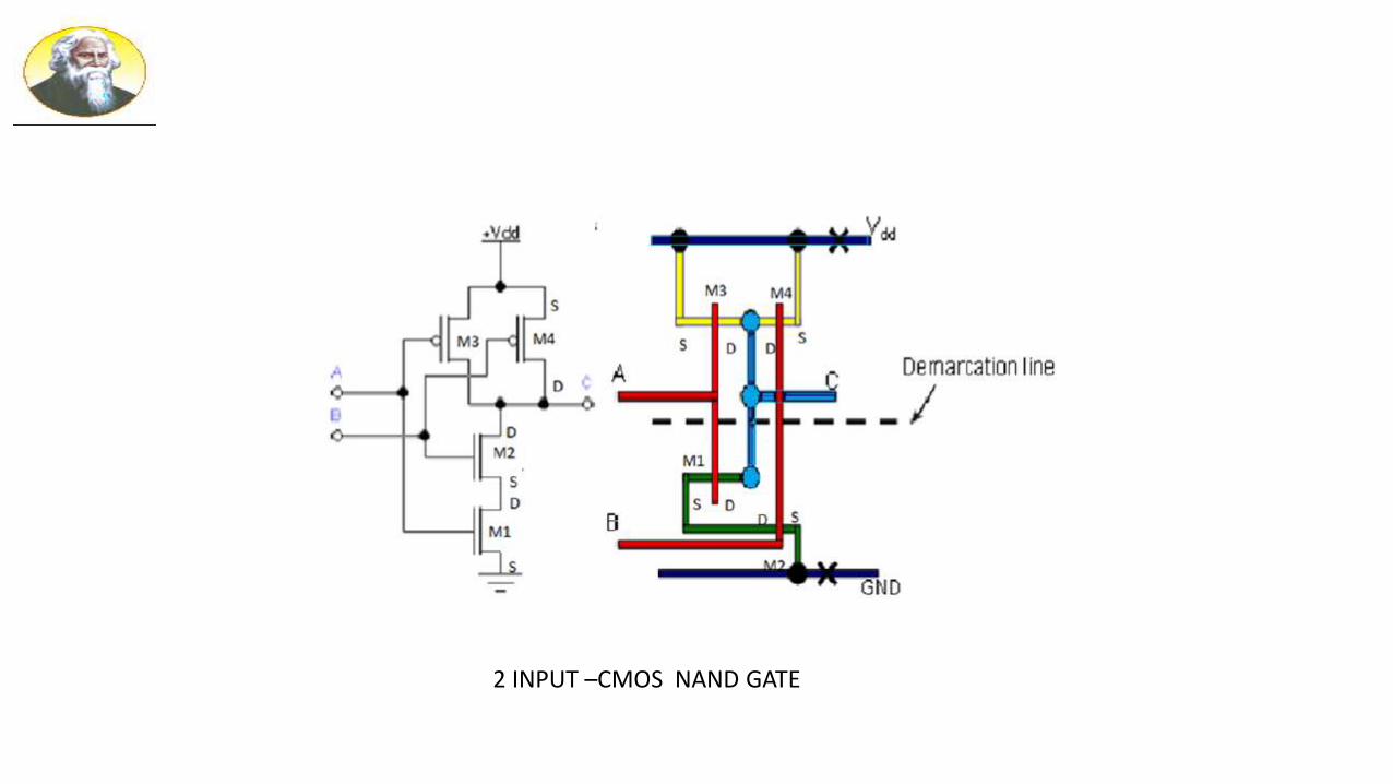
DESIGN RULES AND LAYOUT
Lambda-based Design Rules
Design rules for wires (nMOS and CMOS)

FIGURE Transistor design rules (nMOS, pMOS and CMOS).

FIGURE Contacts (nMOS and CMOS).

2 µm DOUBLE METAL, DOUBLE POLY. CMOS/BICMOS RULES
FIGURE Design rules for wires (interconnects) (Orbit 2 µm CMOS).

FIGURE Two 1/P n.MOS nor gate


VLSI DESIGN FLOW
A design flow is a sequence of operations that transform the ICdesigners’ intention (usually represented in RTL format) into layoutGDSII data. A well-tuned design flow can help designers go throughthe chip-creation process relatively smoothly and with a decentchance of error-free implementation. And, a skilful IC implementationengineer can use the design flow creatively to shorten the designcycle, resulting in a higher likelihood that the product will catch themarket window


Scaling of MOS Circuits
Microelectronic technology may be characterized in terms of several indicators, or
figures of merit. Commonly, the following are used:
• Minimum feature size
• Number of gates on one chip
• Power dissipation
• Maximum operational · frequency
• Die size
• Production cost.
Many of these figures of merit can be improved by shrinking the dimensions of transistors,
interconnections and the separation between features, and by adjusting the doping levels
and
supply voltages

Advantages of Scaling :The reduction in lateral dimensions of the MOSFET and interconnects size is known as 'scaling' of the geometric dimensions of the MOSFET.The advantages of Scaling are as follows,(1) Improved current driving capability improves the device characteristics.(2) Due to small geometries the capacitance reduces.(3) Improved interconnect technology reduces the RC delay.(4) The multiple threshold devices due to scaling adjusts the active and stand by power trade-offs.(5) The integration density improves due to single chip devices.(6) Enhanced performance in terms of speed and power consumption.(7) Cost of a chip decreases by twice.

SCALING MODELS AND SCALIJ.'IIG FACTORS
FIGURE Scaled nMOS transistor (pMOS similar).

SCALING MODELS AND SCALIJ.'IIG FACTORS
The most commonly used models are the constant electric field. scaling model and the
constant
voltage scaling model. They both present a simplified view, taking only first degree effects
into consideration, but are easily understood and well suited to educational needs. Recently,
a combined voltage and dimension scaling model has been presented
In order to accommodate the three models, two scaling factors-1/α and 1/β---ar:e used.
1/ β is chosen as the scaling factor for supply voltage VDD and gate oxide thickness D, and
1/α is used for all other linear. dimensions, both vertical and horizontal to the chip surface.
For the constant field model and the constant voltage model, β = α and β = 1 respectively
are applied
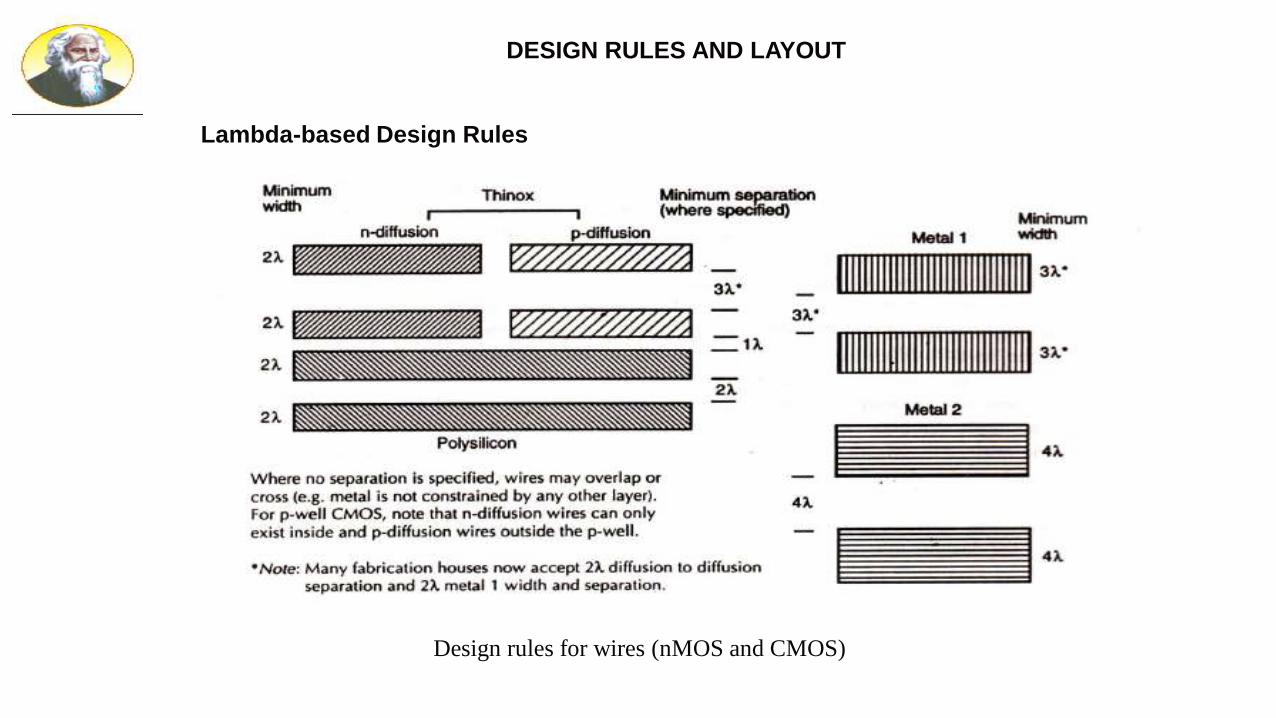
SCALING FACTORS FOR DEVICE PARAMETERS
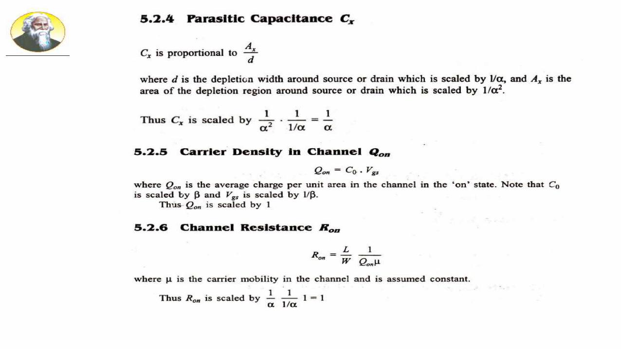


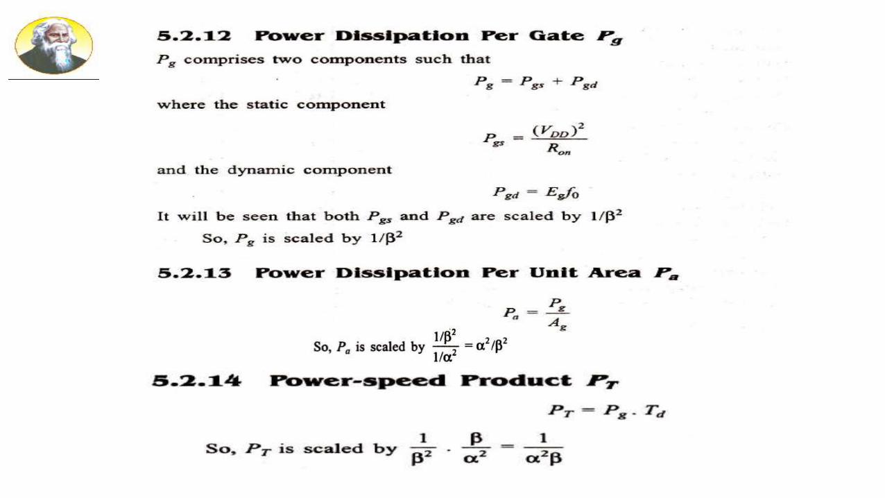

Summary of Scaling Effects