DATASHEET - VLSI · VLSI Solution y DATASHEET VS1001K 2. CHARACTERISTICS & SPECIFICATIONS 2.8...
40
DATASHEET VS1001 K VS1001k - MPEG AUDIO CODEC Features • MPEG audio layer 3 decoder (ISO11172-3) • Supports MPEG 1 & 2, and 2.5 extensions, all their sample rates and bit rates, in mono and stereo • Supports PCM input • Supports VBR (variable bitrate) • Can be used as a slave co-processor • Operates with single clock 12..13 MHz or 24..26 MHz • Low-power operation • On-chip high-quality stereo DAC with no phase error between channels • Internal Op-Amp in BGA-49 and LQFP-48 packages • Stereo earphone driver capable of driving a 30Ω load. • Separate 2.5 .. 3.6V operating voltages for analog and digital • 4 KiB On-chip RAM for user code • Serial control and data interfaces • New functions may be added with software VS_DSP x-RAM x-ROM y-ROM y-RAM program ROM program RAM serial data interface serial control interface stereo DAC audio output DCLK SDATA BSYNC SO SI SCLK XCS DREQ L R VS1001 stereo ear- phone driver X Bus Y Bus I Bus SCI Bus SDI Bus Description VS1001k is a single-chip solution for an MPEG layer 3 audio decoder. The chip contains a high- performance low-power DSP processor (VS DSP), working memory, 4 KiB program RAM and 0.5 KiB data RAM for user applications, serial con- trol and input data interfaces, and a high-quality oversampling variable-sample-rate stereo DAC, fol- lowed by an earphone amplifier and a ground buffer. VS1001k receives its input bitstream through a serial input bus, which it listens to as a system slave. The input stream is decoded and passed through a analog/digital hybrid volume control to an 18-bit oversampling multi-bit sigma-delta DAC. The decoding is controlled via a serial control bus. In addition to the basic decoding, it is possible to add application specific features, like DSP effects, to the user RAM memory. Version 4.14, 2004-02-10 1
Transcript of DATASHEET - VLSI · VLSI Solution y DATASHEET VS1001K 2. CHARACTERISTICS & SPECIFICATIONS 2.8...
VLSISolution y DATASHEET
VS1001K
VS1001k - MPEG AUDIO CODEC
Features
• MPEG audio layer 3 decoder (ISO11172-3)• Supports MPEG 1 & 2, and 2.5 extensions,
all their sample rates and bit rates, in monoand stereo
• Supports PCM input• Supports VBR (variable bitrate)• Can be used as a slave co-processor• Operates with single clock 12..13 MHz or
24..26 MHz• Low-power operation• On-chip high-quality stereo DAC with no
phase error between channels• Internal Op-Amp in BGA-49 and LQFP-48
packages• Stereo earphone driver capable of driving a
30Ω load.• Separate 2.5 .. 3.6V operating voltages for
analog and digital• 4 KiB On-chip RAM for user code• Serial control and data interfaces• New functions may be added with software
VS_DSP x−RAM
x−ROM
y−ROM
y−RAM
programROM
programRAM
serialdatainterface
serialcontrolinterface
stereoDAC
audio
output
DCLKSDATABSYNC
SOSISCLKXCS
DREQ
L
R
VS1001stereo ear−phone driver
X Bus
Y BusI Bus
SCIBus
SDIBus
Description
VS1001k is a single-chip solution for an MPEGlayer 3 audio decoder. The chip contains a high-performance low-power DSP processor (VSDSP),working memory, 4 KiB program RAM and 0.5KiB data RAM for user applications, serial con-trol and input data interfaces, and a high-qualityoversampling variable-sample-rate stereo DAC, fol-lowed by an earphone amplifier and a ground buffer.
VS1001k receives its input bitstream through aserial input bus, which it listens to as a systemslave. The input stream is decoded and passedthrough a analog/digital hybrid volume control toan 18-bit oversampling multi-bit sigma-delta DAC.The decoding is controlled via a serial control bus.In addition to the basic decoding, it is possible toadd application specific features, like DSP effects,to the user RAM memory.
Version 4.14, 2004-02-10 1
VLSISolution y DATASHEET
VS1001K
CONTENTS
Contents
1 License 7
2 Characteristics & Specifications 7
2.1 Analog Characteristics . . . . . . . . . . . . . . . . . . . . . . . . . . . . . . . . . . . 7
2.2 Power Consumption . . . . . . . . . . . . . . . . . . . . . . . . . . . . . . . . . . . . . 8
2.3 DAC Interpolation Filter Characteristics . . . . . . . . . . . . . . . . . . . . . . . . . . 8
2.4 DAC Interpolation Filter Characteristics . . . . . . . . . . . . . . . . . . . . . . . . . . 8
2.5 Absolute Maximum Ratings . . . . . . . . . . . . . . . . . . . . . . . . . . . . . . . . 8
2.6 Recommended Operating Conditions . . . . . . . . . . . . . . . . . . . . . . . . . . . . 9
2.7 Digital Characteristics . . . . . . . . . . . . . . . . . . . . . . . . . . . . . . . . . . . 9
2.8 Switching Characteristics - Clocks . . . . . . . . . . . . . . . . . . . . . . . . . . . . . 10
2.9 Switching Characteristics - DREQ Signal . . . . . . . . . . . . . . . . . . . . . . . . . 10
2.10 Switching Characteristics - SPI Interface Output . . . . . . . . . . . . . . . . . . . . . . 10
2.11 Switching Characteristics - Boot Initialization . . . . . . . . . . . . . . . . . . . . . . . 10
3 Packages and Pin Descriptions 11
3.1 SOIC-28 . . . . . . . . . . . . . . . . . . . . . . . . . . . . . . . . . . . . . . . . . . . 11
3.2 BGA-49 . . . . . . . . . . . . . . . . . . . . . . . . . . . . . . . . . . . . . . . . . . . 12
3.3 LQFP-48 . . . . . . . . . . . . . . . . . . . . . . . . . . . . . . . . . . . . . . . . . . 13
4 Example Connection Diagrams 14
4.1 Connection Diagram, SOIC-28 . . . . . . . . . . . . . . . . . . . . . . . . . . . . . . . 14
4.2 Connection Diagram, BGA-49 . . . . . . . . . . . . . . . . . . . . . . . . . . . . . . . 15
4.3 Connection Diagram, LQFP-48 . . . . . . . . . . . . . . . . . . . . . . . . . . . . . . . 16
Version 4.14, 2004-02-10 2
VLSISolution y DATASHEET
VS1001K
CONTENTS
5 SPI Buses 17
5.1 General . . . . . . . . . . . . . . . . . . . . . . . . . . . . . . . . . . . . . . . . . . . 17
5.2 SPI Bus Pin Descriptions . . . . . . . . . . . . . . . . . . . . . . . . . . . . . . . . . . 17
5.3 Serial Protocol for Serial Data Interface (SDI) . . . . . . . . . . . . . . . . . . . . . . . 17
5.4 Serial Protocol for Serial Command Interface (SCI) . . . . . . . . . . . . . . . . . . . . 18
5.4.1 General . . . . . . . . . . . . . . . . . . . . . . . . . . . . . . . . . . . . . . . 18
5.4.2 SCI Read . . . . . . . . . . . . . . . . . . . . . . . . . . . . . . . . . . . . . . 18
5.4.3 SCI Write . . . . . . . . . . . . . . . . . . . . . . . . . . . . . . . . . . . . . . 19
5.5 SPI Timing Diagram . . . . . . . . . . . . . . . . . . . . . . . . . . . . . . . . . . . . 20
6 Functional Description 21
6.1 Main Features . . . . . . . . . . . . . . . . . . . . . . . . . . . . . . . . . . . . . . . . 21
6.2 Data Flow of VS1001k . . . . . . . . . . . . . . . . . . . . . . . . . . . . . . . . . . . 21
6.3 Serial Data Interface (SDI) . . . . . . . . . . . . . . . . . . . . . . . . . . . . . . . . . 22
6.4 Serial Control Interface (SCI) . . . . . . . . . . . . . . . . . . . . . . . . . . . . . . . . 22
6.5 SCI Registers . . . . . . . . . . . . . . . . . . . . . . . . . . . . . . . . . . . . . . . . 22
6.5.1 MODE (RW) . . . . . . . . . . . . . . . . . . . . . . . . . . . . . . . . . . . . 23
6.5.2 STATUS (RW) . . . . . . . . . . . . . . . . . . . . . . . . . . . . . . . . . . . 25
6.5.3 INT FCNTLH (-) . . . . . . . . . . . . . . . . . . . . . . . . . . . . . . . . . . 25
6.5.4 CLOCKF (RW) . . . . . . . . . . . . . . . . . . . . . . . . . . . . . . . . . . . 25
6.5.5 DECODETIME (R) . . . . . . . . . . . . . . . . . . . . . . . . . . . . . . . . 25
6.5.6 AUDATA (R) . . . . . . . . . . . . . . . . . . . . . . . . . . . . . . . . . . . . 26
6.5.7 WRAM (W) . . . . . . . . . . . . . . . . . . . . . . . . . . . . . . . . . . . . 26
6.5.8 WRAMADDR (W) . . . . . . . . . . . . . . . . . . . . . . . . . . . . . . . . . 26
6.5.9 HDAT0 and HDAT1 (R) . . . . . . . . . . . . . . . . . . . . . . . . . . . . . . 27
Version 4.14, 2004-02-10 3
VLSISolution y DATASHEET
VS1001K
CONTENTS
6.5.10 AIADDR (RW) . . . . . . . . . . . . . . . . . . . . . . . . . . . . . . . . . . . 28
6.5.11 VOL (RW) . . . . . . . . . . . . . . . . . . . . . . . . . . . . . . . . . . . . . 28
6.5.12 RESERVED (RW) . . . . . . . . . . . . . . . . . . . . . . . . . . . . . . . . . 28
6.5.13 AICTRL[x] (RW) . . . . . . . . . . . . . . . . . . . . . . . . . . . . . . . . . . 28
6.6 Stereo Audio DAC . . . . . . . . . . . . . . . . . . . . . . . . . . . . . . . . . . . . . 28
7 Operation 29
7.1 Clocking . . . . . . . . . . . . . . . . . . . . . . . . . . . . . . . . . . . . . . . . . . . 29
7.2 Powerdown . . . . . . . . . . . . . . . . . . . . . . . . . . . . . . . . . . . . . . . . . 29
7.3 Hardware Reset . . . . . . . . . . . . . . . . . . . . . . . . . . . . . . . . . . . . . . . 29
7.4 Software Reset . . . . . . . . . . . . . . . . . . . . . . . . . . . . . . . . . . . . . . . 29
7.5 Play/Decode . . . . . . . . . . . . . . . . . . . . . . . . . . . . . . . . . . . . . . . . . 30
7.6 Sanity Checks . . . . . . . . . . . . . . . . . . . . . . . . . . . . . . . . . . . . . . . . 30
7.7 PCM Mode . . . . . . . . . . . . . . . . . . . . . . . . . . . . . . . . . . . . . . . . . 30
7.8 Testing . . . . . . . . . . . . . . . . . . . . . . . . . . . . . . . . . . . . . . . . . . . . 30
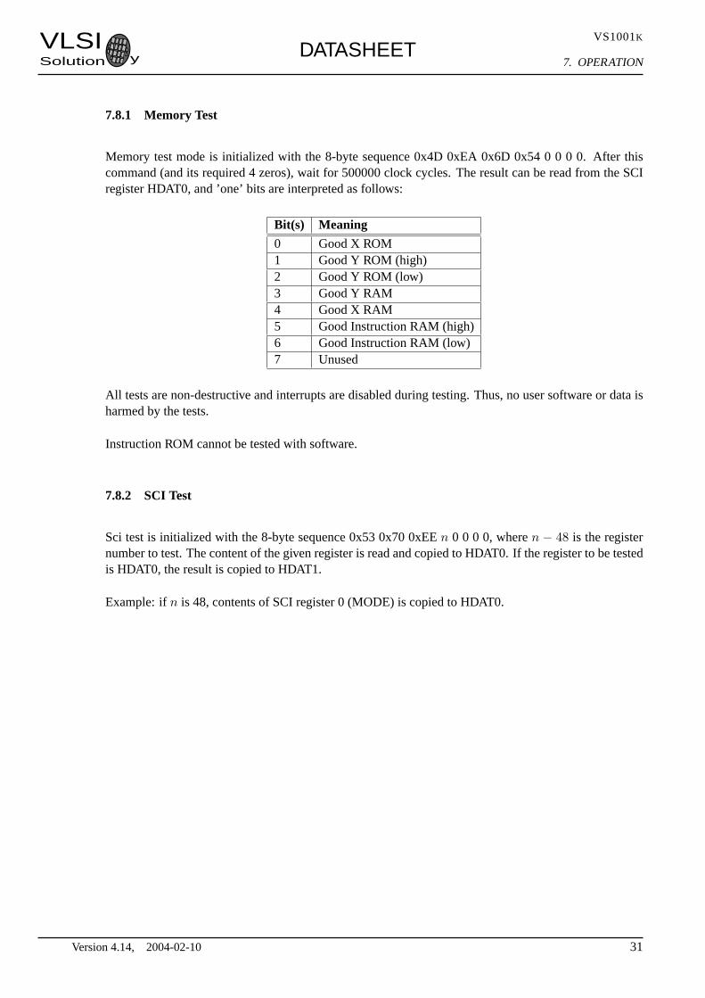
7.8.1 Memory Test . . . . . . . . . . . . . . . . . . . . . . . . . . . . . . . . . . . . 31
7.8.2 SCI Test . . . . . . . . . . . . . . . . . . . . . . . . . . . . . . . . . . . . . . . 31
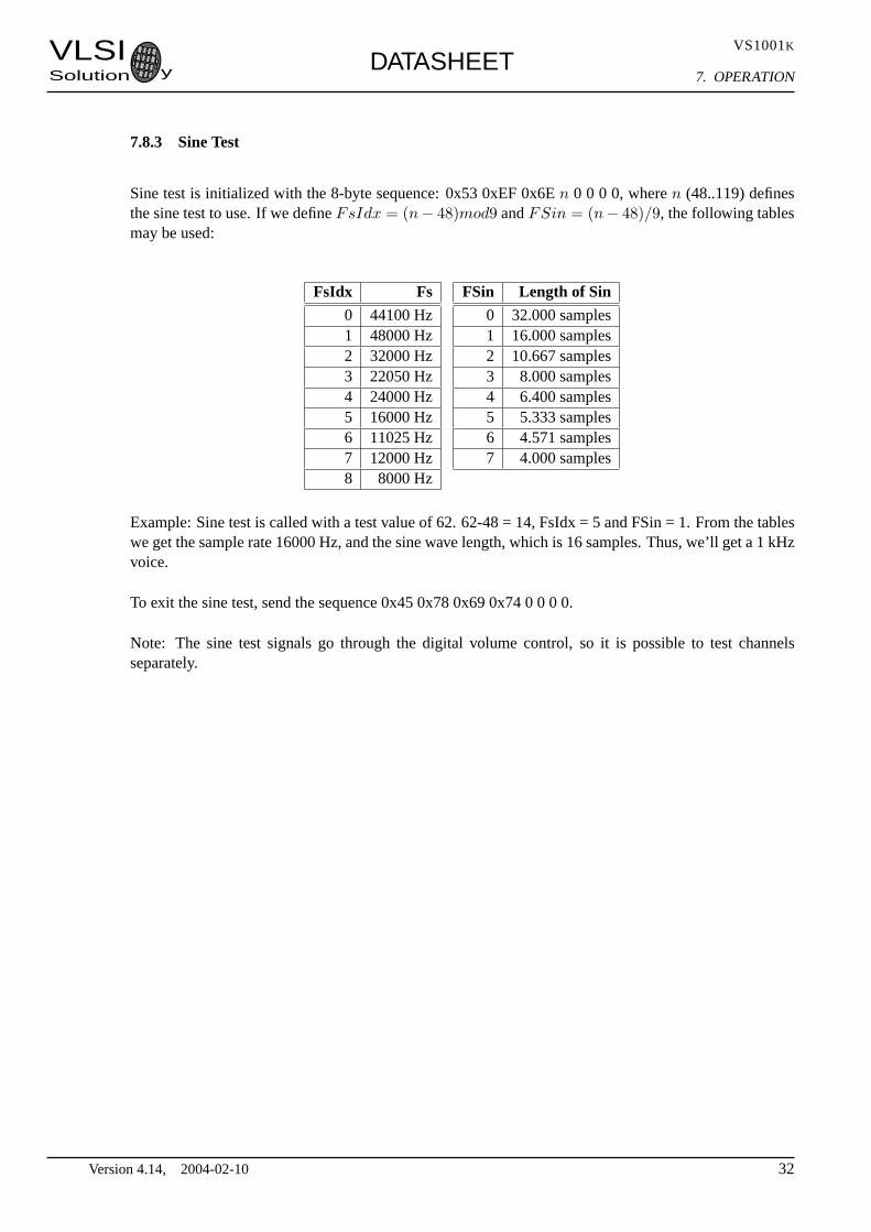
7.8.3 Sine Test . . . . . . . . . . . . . . . . . . . . . . . . . . . . . . . . . . . . . . 32
8 Writing Software 33
8.1 When to Write Software . . . . . . . . . . . . . . . . . . . . . . . . . . . . . . . . . . 33
8.2 The Processor Core . . . . . . . . . . . . . . . . . . . . . . . . . . . . . . . . . . . . . 33
8.3 User’s Memory Map . . . . . . . . . . . . . . . . . . . . . . . . . . . . . . . . . . . . 33
8.4 Hardware Registers . . . . . . . . . . . . . . . . . . . . . . . . . . . . . . . . . . . . . 33
8.4.1 SCI Registers, 0x4000 . . . . . . . . . . . . . . . . . . . . . . . . . . . . . . . 33
8.4.2 Serial Registers, 0x4100 . . . . . . . . . . . . . . . . . . . . . . . . . . . . . . 33
Version 4.14, 2004-02-10 4
VLSISolution y DATASHEET
VS1001K
CONTENTS
8.4.3 DAC Registers, 0x4200 . . . . . . . . . . . . . . . . . . . . . . . . . . . . . . . 34
8.4.4 Interrupt Registers, 0x4300 . . . . . . . . . . . . . . . . . . . . . . . . . . . . . 34
8.5 System Vector Tags . . . . . . . . . . . . . . . . . . . . . . . . . . . . . . . . . . . . . 35
8.5.1 AudioInt, 0x4000..0x4001 . . . . . . . . . . . . . . . . . . . . . . . . . . . . . 35
8.5.2 SpiInt, 0x4002..0x4003 . . . . . . . . . . . . . . . . . . . . . . . . . . . . . . . 35
8.5.3 DataInt, 0x4004..0x4005 . . . . . . . . . . . . . . . . . . . . . . . . . . . . . . 35
8.5.4 UserCodec, 0x4008..0x4009 . . . . . . . . . . . . . . . . . . . . . . . . . . . . 35
8.6 System Vector Functions . . . . . . . . . . . . . . . . . . . . . . . . . . . . . . . . . . 36
8.6.1 WriteIRam(), 0x4010 . . . . . . . . . . . . . . . . . . . . . . . . . . . . . . . . 36
8.6.2 ReadIRam(), 0x4011 . . . . . . . . . . . . . . . . . . . . . . . . . . . . . . . . 36
8.6.3 DataWords(), 0x4012 . . . . . . . . . . . . . . . . . . . . . . . . . . . . . . . . 37
8.6.4 GetDataByte(), 0x4013 . . . . . . . . . . . . . . . . . . . . . . . . . . . . . . . 37
8.6.5 GetDataWords(), 0x4014 . . . . . . . . . . . . . . . . . . . . . . . . . . . . . . 37
9 VS1001 Version Changes 38
9.1 Changes Between VS1001h and Production Version VS1001k, 2001-08 . . . . . . . . . 38
9.2 Changes Between VS1001g and VS1001h, 2001-05 . . . . . . . . . . . . . . . . . . . . 38
9.3 Changes Between VS1001d to VS1001g, 2001-03 . . . . . . . . . . . . . . . . . . . . . 38
10 Document Version Changes 39
10.1 Changes Between Version 4.13 and 4.14 for VS1001k, 2004-02 . . . . . . . . . . . . . 39
10.2 Changes Between Version 4.12 and 4.13 for VS1001k, 2003-11 . . . . . . . . . . . . . 39
10.3 Changes Between Version 4.11 and 4.12 for VS1001k, 2003-10 . . . . . . . . . . . . . 39
10.4 Changes Between Version 4.10 and 4.11 for VS1001k, 2003-09 . . . . . . . . . . . . . 39
10.5 Changes Between Version 4.08 and 4.10 for VS1001k, 2003-07 . . . . . . . . . . . . . 39
10.6 Changes Between Version 4.07 and 4.08 for VS1001k, 2003-03 . . . . . . . . . . . . . 39
Version 4.14, 2004-02-10 5
VLSISolution y DATASHEET
VS1001K
LIST OF FIGURES
11 Contact Information 40
List of Figures
1 Pin Configuration, SOIC-28. . . . . . . . . . . . . . . . . . . . . . . . . . . . . . . . . 11
2 Pin Configuration, BGA-49. . . . . . . . . . . . . . . . . . . . . . . . . . . . . . . . . 12
3 Pin Configuration, LQFP-48. . . . . . . . . . . . . . . . . . . . . . . . . . . . . . . . . 13
4 Typical Connection Diagram Using SOIC-28. . . . . . . . . . . . . . . . . . . . . . . . 14
5 Typical Connection Diagram Using BGA-49. . . . . . . . . . . . . . . . . . . . . . . . 15
6 Typical Connection Diagram Using LQFP-48. . . . . . . . . . . . . . . . . . . . . . . . 16
7 BSYNC Signal. . . . . . . . . . . . . . . . . . . . . . . . . . . . . . . . . . . . . . . . 17
8 SCI Word Read . . . . . . . . . . . . . . . . . . . . . . . . . . . . . . . . . . . . . . . 19
9 SCI Word Write . . . . . . . . . . . . . . . . . . . . . . . . . . . . . . . . . . . . . . . 19
10 SPI Timing Diagram. . . . . . . . . . . . . . . . . . . . . . . . . . . . . . . . . . . . . 20
11 Data Flow of VS1001k. . . . . . . . . . . . . . . . . . . . . . . . . . . . . . . . . . . . 21
12 Built-In Bass/Treble Enhancer Frequency Response at 44.1 kHz. . . . . . . . . . . . . . 24
13 User’s Memory Map. . . . . . . . . . . . . . . . . . . . . . . . . . . . . . . . . . . . . 34
Version 4.14, 2004-02-10 6
VLSISolution y DATASHEET
VS1001K
1. LICENSE
1 License
MPEG Layer-3 audio decoding technology licensed from Fraunhofer IIS and Thomson.
2 Characteristics & Specifications
Unless otherwise noted: AVDD=2.9..3.6V, DVDD=2.3..3.6V, TA=-30..+85C, XTALI=24.576MHz, Full-Scale Output Sinewave at 1.526 kHz, measurement bandwidth 20..20000 Hz, analog output load 30Ω (noground buffer) or 100Ω (with ground buffer), bitstream 128 kbits/s, local components as shown in Figures4 and 5.
Note, that some analog values are in practice better than in these tables if chips are used within a limitedtemperature range and not too close to lower voltage limits.
2.1 Analog Characteristics
Parameter Symbol Min Typ Max Unit
DAC Resolution 16 bitsTotal Harmonic Distortion THD 0.1 0.2 %Dynamic Range (DAC unmuted, A-weighted) IDR 90 dBS/N Ratio (full scale signal) SNR 70 87 dBInterchannel Isolation 50 75 dBInterchannel Gain Mismatch -0.5 0.5 dBFrequency Response -0.1 0.1 dBFrequency Response, AVDD = 2.8V -0.3 0.3 dBFull Scale Output Voltage (Peak-to-peak) 1.4 1.81 2.0 VppDeviation from Linear Phase 5
Out of Band Energy -60 dBOut of Band Energy with Analog Filter -90 dBAnalog Output Load Resistance, no ground bufferAOLR1 16 302 ΩAnalog Output Load Resistance, ground buffer AOLR2 16 1002 ΩAnalog Output Load Capacitance 1000 pF
1 3.6 volts can be achieved with +-to-+ wiring for mono difference sound.2 AOLR1/2 may be much lower, but belowTypicaldistortion performance may be compromised.
Version 4.14, 2004-02-10 7
VLSISolution y DATASHEET
VS1001K
2. CHARACTERISTICS & SPECIFICATIONS
2.2 Power Consumption
Parameter Symbol Min Typ Max Unit
Power Supply Rejection 40 dBPower Supply Consumption AVDD, Reset 0.6 5.0 µAPower Supply Consumption AVDD, no load 3.0 4.5 6.0 mAPower Supply Consumption AVDD, output loaded at 30Ω 4.0 5.5 40.0 mAPower Supply Consumption AVDD, o. @ 30Ω + GND-buf. 6.0 7.5 40.0 mAPower Supply Consumption DVDD, Reset 3.7 100.0 µAPower Supply Consumption DVDD 15.0 mA
2.3 DAC Interpolation Filter Characteristics
Parameter Symbol Min Typ Max Unit
Passband (to -3dB corner) 0 0.459Fs HzPassband (Ripple Spec) 0 0.420Fs HzPassband Ripple ±0.056 dBTransition Band 0.420Fs 0.580Fs HzStop Band 0.580Fs HzStop Band Rejection 90 dBGroup Delay 15/Fs s
Fs is conversion frequency
2.4 DAC Interpolation Filter Characteristics
Parameter Symbol Min Typ Max Unit
-3 dB bandwidth 300 kHzPassband Response at 20 kHz -0.05 dB
2.5 Absolute Maximum Ratings
Parameter Symbol Min Max Unit
Analog Positive Supply AVDD -0.3 3.6 VDigital Positive Supply DVDD -0.3 3.6 VCurrent at Any Digital Output ±50 mAVoltage at Any Digital Input DGND-1.0 DVDD+1.0 VOperating Temperature -30 +85 CFunctional Operating Temperature -40 +95 CStorage Temperature -65 +150 C
Version 4.14, 2004-02-10 8
VLSISolution y DATASHEET
VS1001K
2. CHARACTERISTICS & SPECIFICATIONS
2.6 Recommended Operating Conditions
Parameter Symbol Min Typ Max Unit
Analog and Digital Ground AGND DGND 0.0 VPositive Analog AVDD 2.51 3.0 3.6 VAmbient Operating Temperature -30 +85 C
1 If AVDD is below 2.8 V, distortion performance may be compromised.
The following values are to be used when the clock doubler is active:
Parameter Symbol Min Typ Max Unit
Positive Digital DVDD 2.3 2.7 3.6 VInput Clock Frequency XTALI 12.288 13 MHzInternal Clock Frequency1 CLKI 24.576 26 MHz
1 The maximum sample rate that may be decoded with correct speed is CLKI/512.
The following values are to be used when the clock doubler is inactive:
Parameter Symbol Min Typ Max Unit
Positive Digital DVDD 2.3 2.7 3.6 VInput Clock Frequency XTALI 24.576 26 MHzInternal Clock Frequency1 CLKI 24.576 26 MHz
1 The maximum sample rate that may be decoded with correct speed is CLKI/512.
Note: With higher than typical voltages, VS1001k may operate with CLKI upto 30..32 MHz. However,the chips are not qualified for this kind of usage. If necessary, VLSI Solution Oy can qualify chips forhigher clock rates for quantity orders.
2.7 Digital Characteristics
Parameter Symbol Min Typ Max Unit
High-Level Input Voltage 0.7DVDD VLow-Level Input Voltage 0.3DVDD VHigh-Level Output Voltage at IO = -2.0 mA 0.7DVDD VLow-Level Output Voltage at IO = 2.0 mA 0.3DVDD VInput Leakage Current 1.0 µA
Version 4.14, 2004-02-10 9

VLSISolution y DATASHEET
VS1001K
2. CHARACTERISTICS & SPECIFICATIONS
2.8 Switching Characteristics - Clocks
Parameter Symbol Min Typ Max Unit
Master Clock Frequency1 XTALI 12.288 MHzMaster Clock Frequency2 XTALI 24.576 MHzMaster Clock Duty Cycle 40 50 60 %Clock Output XTALO XTALI MHz
1 Clock doubler active.2 Clock doubler inactive.
2.9 Switching Characteristics - DREQ Signal
Parameter Symbol Min Typ Max Unit
Data Request Signal DREQ 200 ns
2.10 Switching Characteristics - SPI Interface Output
Parameter Symbol Min Typ Max Unit
SPI Input Clock Frequency 0.25×CLKI MHzRise time for SO 100 ns
2.11 Switching Characteristics - Boot Initialization
Parameter Symbol Min Max Unit
RESET active time 2 XTALIRESET inactive to software ready 50000 XTALI
Version 4.14, 2004-02-10 10
VLSISolution y DATASHEET
VS1001K
3. PACKAGES AND PIN DESCRIPTIONS
3 Packages and Pin Descriptions
3.1 SOIC-28
SOIC − 28
1413121110987654321XRESET
DVDD
DGND
AVDD
AGND
XCS
SCLK
SI
SO
SDATA
DCLK
BSYNC
DREQ
XTALI
XTALO
LEFT
RIGHT
TEST1
TEST0
TEST2
AGND
AVDD
DVDD
DGND
DVDD
DGND
1516171819202122232728
RCAP
AGND
26 2425
VS1001
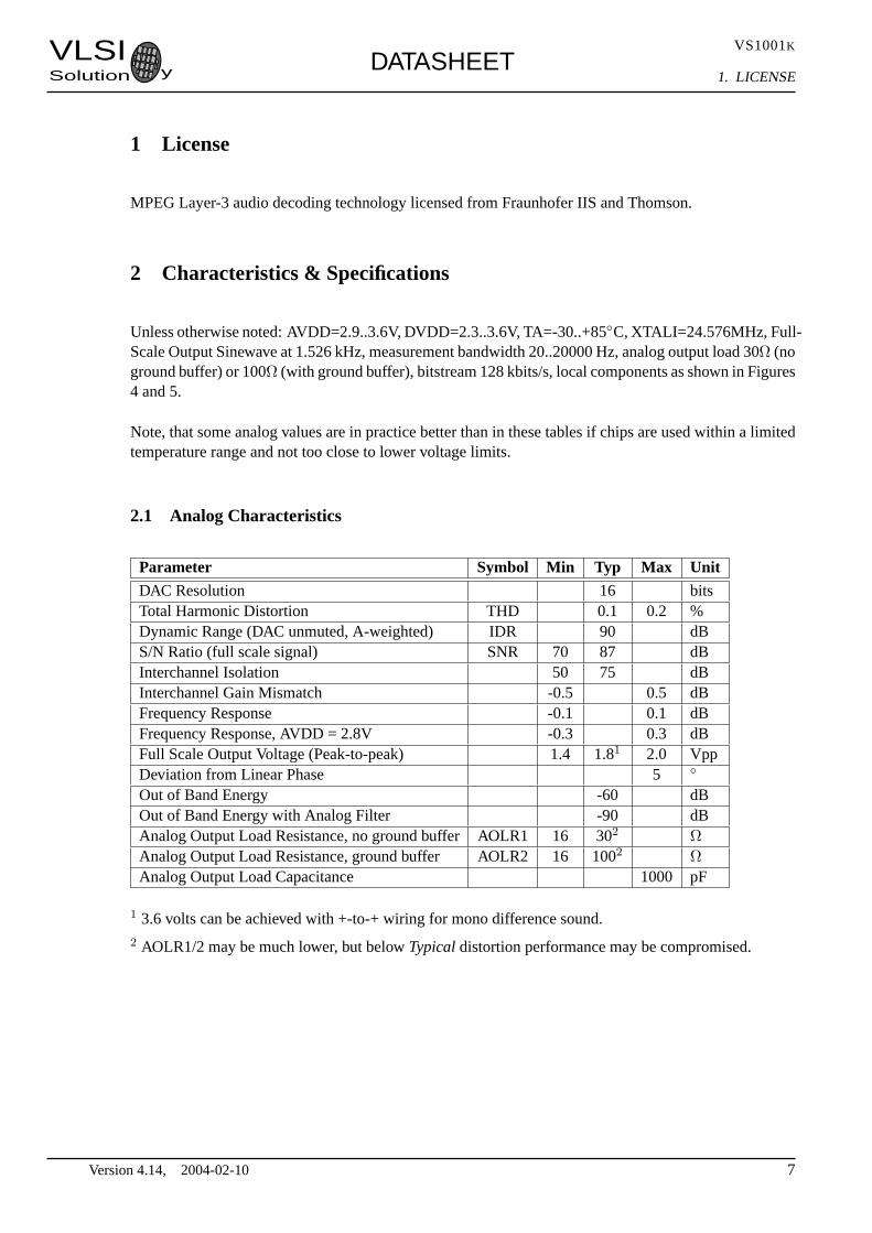
Figure 1: Pin Configuration, SOIC-28.
Pin Name Pin Pin Type Function
DREQ 1 DO data request, input busDCLK 2 DIO serial input data bus clockSDATA 3 DI serial data inputBSYNC 4 DI byte synchronization signalDVDD1 5 PWR digital power supplyDGND1 6 PWR digital groundXTALO 7 CLK crystal outputXTALI 8 CLK crystal inputDVDD2 9 PWR digital power supplyDGND2 10 PWR digital groundXCS 11 DI chip select input (active low)SCLK 12 DI clock for serial busSI 13 DI serial inputSO 14 DO3 serial outputTEST0 15 DI reserved for test, connect to DVDDTEST1 16 DO reserved for test,do not connect!TEST2 17 DO reserved for test,do not connect!AGND1 18 PWR analog groundAVDD1 19 PWR analog power supplyRIGHT 20 AO right channel outputAGND2 21 PWR analog groundRCAP 22 AIO filtering capacitance for referenceAVDD2 23 PWR analog power supplyLEFT 24 AO left channel outputAGND3 25 PWR analog groundXRESET 26 DI active low asynchronous resetDGND3 27 PWR digital groundDVDD3 28 PWR digital power supply
Pin types:Type DescriptionDI Digital input, CMOS Input PadDO Digital output, CMOS Input PadDIO Digital input/outputDO3 Digital output, CMOS Tri-stated Output Pad
Type DescriptionAI Analog inputAO Analog outputAIO Analog input/outputPWR Power supply pin
SOIC-28 package dimensions can be found athttp://www.vlsi.fi/vs1001/soic28.pdf.
Version 4.14, 2004-02-10 11

VLSISolution y DATASHEET
VS1001K
3. PACKAGES AND PIN DESCRIPTIONS
3.2 BGA-49
A
B
C
D
E
F
G
1 2 3 4 5 6 7
TOP VIEW
0.80
TY
P
4.80
7.00
1.10
RE
F
0.80 TYP1.10 REF
4.80
7.00
A1 BALL PAD CORNER
Figure 2: Pin Configuration, BGA-49.
Pin Name Ball Pin Type Function
BSYNC E3 DI byte synchronization signalDVDD1 F3 PWR digital power supplyDGND1 F4 PWR digital groundXTAL0 G3 CLK crystal outputXTALI E4 CLK crystal inputDVDD2 F5 PWR digital power supplyDGND2 F6 PWR digital groundXCS G6 DI chip select input (active low)SCLK D6 DI clock for serial busSI E7 DI serial inputSO D5 DO3 serial outputTEST0 C6 DI reserved for test, connect to DVDDTEST1 C7 DO reserved for test,do not connect!TEST2 B6 DO reserved for test,do not connect!AGND1 C5 PWR analog groundAVDD1 B5 PWR analog power supplyRIGHT A6 AO right channel outputAGND34 B4 PWR analog groundGBGND A5 PWR analog ground for ground bufferGBUF C4 AO ground bufferGBVDD A4 PWR analog power supply for ground bufferRCAP B3 AIO filtering capacitance for referenceAVDD45 A3 PWR analog power supplyLEFT B2 AO left channel outputAGND56 A2 PWR analog groundXRESET B1 DI active low asynchronous resetDGND3 D2 PWR digital groundDVDD3 D3 PWR digital power supplyDREQ E2 DO data request, input busDCLK E1 DIO serial input data bus clockSDATA F2 DI serial data input
Not connected are: A1, A7, B7, C1, C2, C3, D1, D4, D7, E5, E6, F1, F7, G1, G2, G4, G5 and G7. For“Pin Types”, see Chapter 3.1. BGA-49 package dimensions are athttp://www.vlsi.fi/vs1001/bga49.pdf.
Version 4.14, 2004-02-10 12

VLSISolution y DATASHEET
VS1001K
3. PACKAGES AND PIN DESCRIPTIONS
3.3 LQFP-48
148
Figure 3: Pin Configuration, LQFP-48.
Pin Name Pin Pin Type Function
nc 1,2 -XRESET 3 DI active low asynchronous resetDGND0 4 PWR digital groundnc 5 -DVDD0 6 PWR digital power supplync 7 -DREQ 8 DO data request, input busDCLK 9 DI serial input data bus clockSDATA 10 DI serial data inputnc 11,12 -BSYNC 13 DI byte synchronization signalDVDD1 14 PWR digital power supplync 15 -DGND1 16 PWR digital groundXTALO 17 AO crystal outputXTALI 18 AI crystal inputDVDD2 19 PWR digital power supplyDGND2 20 PWR digital groundDGND3 21 PWR digital groundDGND4 22 PWR digital groundXCS 23 DI chip select input (active low)nc 24. . . 27 -SCLK 28 DI clock for serial busSI 29 DI serial inputSO 30 DO3 serial outputnc 31 -TEST0 32 DI reserved for test, connect to DVDDTEST1 33 DO reserved for test,do not connect!TEST2 34 DO reserved for test,do not connect!nc 35,36 -AGND0 37 PWR analog ground, low-noise referenceAVDD0 38 PWR analog power supplyRIGHT 39 AO right channel outputAGND1 40 PWR analog groundGBGND 41 PWR analog groundGBUF 42 AO ground bufferGBVDD 43 PWR analog power supplyRCAP 44 AIO filtering capacitance for referenceAVDD1 45 PWR analog power supplyLEFT 46 AO left channel outputAGND2 47 PWR analog groundnc 48 -
For “Pin Types”, see Chapter 3.1. LQFP-48 package dimensions are athttp://www.vlsi.fi/vs1001/lqfp48.pdf.
Version 4.14, 2004-02-10 13
VLSISolution y DATASHEET
VS1001K
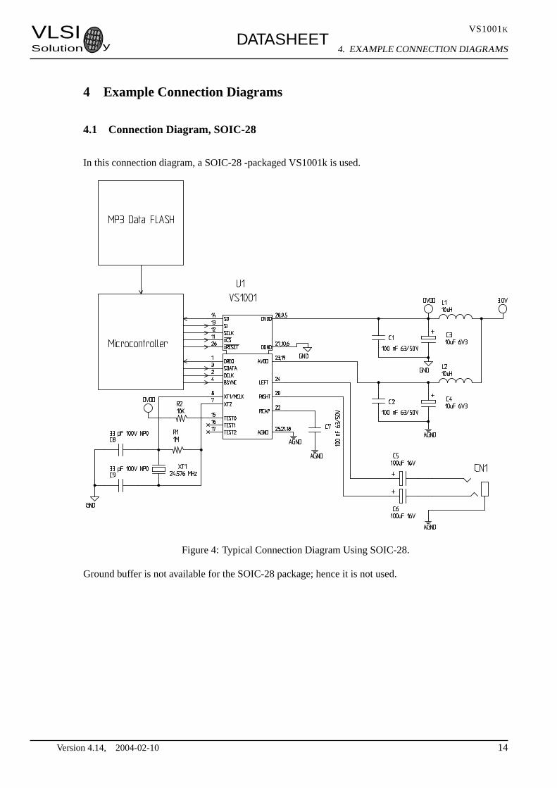
4. EXAMPLE CONNECTION DIAGRAMS
4 Example Connection Diagrams
4.1 Connection Diagram, SOIC-28
In this connection diagram, a SOIC-28 -packaged VS1001k is used.
Figure 4: Typical Connection Diagram Using SOIC-28.
Ground buffer is not available for the SOIC-28 package; hence it is not used.
Version 4.14, 2004-02-10 14

VLSISolution y DATASHEET
VS1001K
4. EXAMPLE CONNECTION DIAGRAMS
4.2 Connection Diagram, BGA-49
In this connection diagram, a BGA-49 packaged VS1001k is used. In this picture, ground buffer is active.
Figure 5: Typical Connection Diagram Using BGA-49.
Ground buffer GBUF can be used for common voltage (1.37 V) for earphones. This will eliminate theneed for large isolation capacitors on line outputs, and thus the audio output pins from VS1001k may beconnected directly to the earphone connector.
If GBUF is not used, GBGND and GBVDD should not be connected. In addition, LEFT and RIGHTmust be provided with 100µF capacitors.
Version 4.14, 2004-02-10 15

VLSISolution y DATASHEET
VS1001K
4. EXAMPLE CONNECTION DIAGRAMS
4.3 Connection Diagram, LQFP-48
In this connection diagram, a LQFP-48 packaged VS1001k is used. In this picture, ground buffer isactive.
Figure 6: Typical Connection Diagram Using LQFP-48.
Ground buffer GBUF can be used for common voltage (1.37 V) for earphones. This will eliminate theneed for large isolation capacitors on line outputs, and thus the audio output pins from VS1001k may beconnected directly to the earphone connector.
If GBUF is not used, GBGND and GBVDD should not be connected. In addition, LEFT and RIGHTmust be provided with 100µF capacitors.
Version 4.14, 2004-02-10 16
VLSISolution y DATASHEET
VS1001K
5. SPI BUSES
5 SPI Buses
5.1 General
The SPI Bus - that was originally used in some Motorola devices - has been used for both VS1001k’sSerial Data Interface SDI (Chapters 5.3 and 6.3) and Serial Control Interface SCI (Chapters 5.4 and 6.4).
5.2 SPI Bus Pin Descriptions
SDI Pin SCI Pin Description
- XCS Active low chip select input. A high level forces the serial interface intostandby mode, ending the current operation. A high level also forces serialoutput (SO) to high impedance state. There is no chip select for SDI, whichis always active.
DCLK SCK Serial clock input. The serial clock is also used internally as the masterclock for the register interface.SCK can be gated or continuous. In either case, the first rising clock edgeafter XCS has gone low marks the first bit to be written (clock 0 in thefollowing figures).
SDATA SI Serial input. SI is sampled on the rising SCK edge, if XCS is low.- SO Serial output. In reads, data is shifted out on the falling SCK edge.
In writes SO is at a high impedance state.
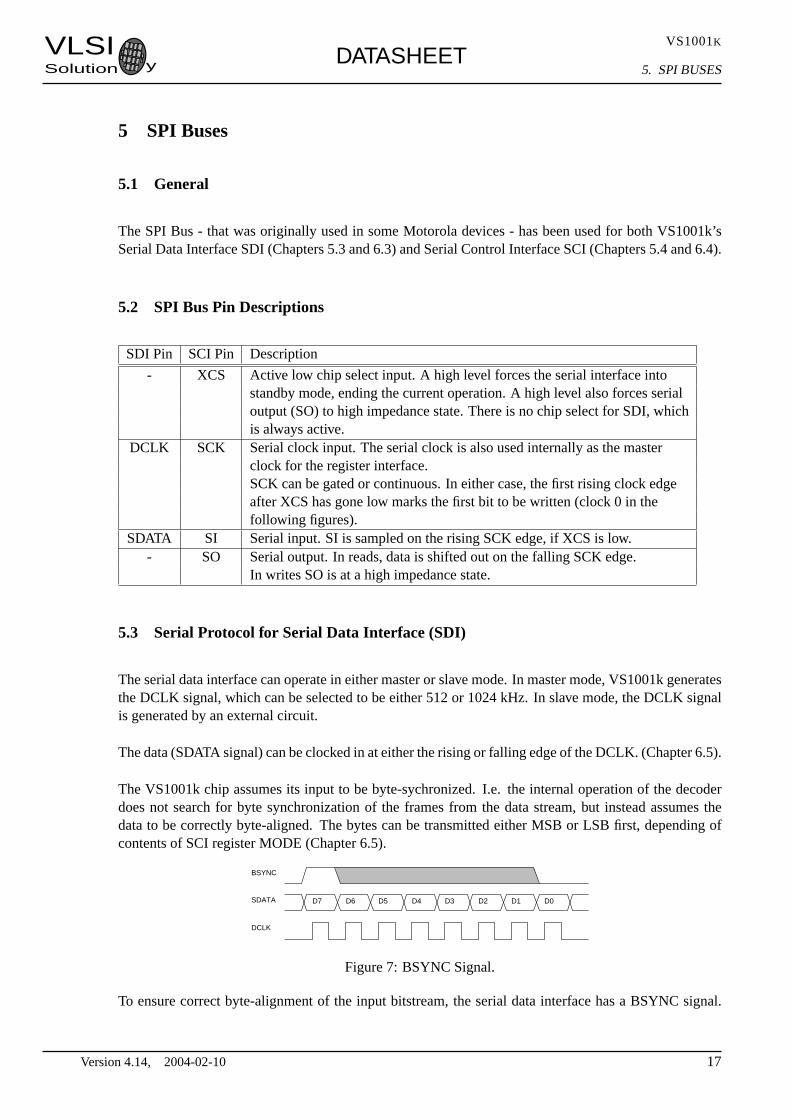
5.3 Serial Protocol for Serial Data Interface (SDI)
The serial data interface can operate in either master or slave mode. In master mode, VS1001k generatesthe DCLK signal, which can be selected to be either 512 or 1024 kHz. In slave mode, the DCLK signalis generated by an external circuit.
The data (SDATA signal) can be clocked in at either the rising or falling edge of the DCLK. (Chapter 6.5).
The VS1001k chip assumes its input to be byte-sychronized. I.e. the internal operation of the decoderdoes not search for byte synchronization of the frames from the data stream, but instead assumes thedata to be correctly byte-aligned. The bytes can be transmitted either MSB or LSB first, depending ofcontents of SCI register MODE (Chapter 6.5).
BSYNC
SDATA
DCLK
D7 D6 D5 D4 D3 D2 D1 D0
Figure 7: BSYNC Signal.
To ensure correct byte-alignment of the input bitstream, the serial data interface has a BSYNC signal.
Version 4.14, 2004-02-10 17
VLSISolution y DATASHEET
VS1001K
5. SPI BUSES
The first DCLK sampling edge (rising or falling, depending on selected polarity), during which theBSYNC is high, marks the first bit of a byte (LSB, if LSB-first order is used, MSB, if MSB-first orderis used). If BSYNC is not used, it must be tied to VCC externally and the master of the input serialinterface must always sustain the correct byte-alignment. Using BSYNC is strongly recommended. Formore details, look at the Application Notes for VS10XX.
The DREQ signal of the data interface is used in slave mode to signal if VS1001k’s FIFO is capable ofreceiving more input data. If DREQ is high, VS1001k can take at least 32 bytes of data. When there isless than 32 bytes of free space, DREQ is turned low, and the sender should stop transferring new data.Because of the 32-byte safety area, the sender may send upto 32 bytes of data at a time without checkingthe status of DREQ, making controlling VS1001k easier for low-speed microcontrollers.
Note: DREQ may turn low or high at any time, even during a byte transmission. Thus, DREQ shouldonly be used to decide whether to send more bytes. It should not abort a transmission that has alreadystarted.
5.4 Serial Protocol for Serial Command Interface (SCI)
5.4.1 General
The serial bus protocol for the Serial Command Interface SCI (Chapter 6.4) consists of an instructionbyte, address byte and one 16-bit data word. Each read or write operation can read or write a singleregister. Data bits are read at the rising edge, so the user should not update data at the rising edge.
The operation is specified by an 8-bit instruction opcode. The supported instructions are read and write.See table below.
InstructionName Opcode Operation
READ 0000 0011 Read dataWRITE 0000 0010 Write data
Note: After using the Serial Command Interface, it is not allowed to send SCI or SDI data for 5 mi-croseconds.
5.4.2 SCI Read
VS1001k registers are read by the following sequence. First, XCS line is pulled low to select the device.Then the READ opcode (0x3) is transmitted via the SI line followed by an 8-bit word address. After theaddress has been read in, any further data on SI is ignored. The 16-bit data corresponding to the receivedaddress will be shifted out onto the SO line.
XCS should be driven high after the data has been shifted out. In that case, the word address will beincremented and data corresponding to the next address will be shifted out. After the last word has beenshifted out, XCS should be driven high to end the READ sequence.
Version 4.14, 2004-02-10 18
VLSISolution y DATASHEET
VS1001K
5. SPI BUSES
Word read is shown in Figure 8.
0 0 0 0 0 0 1 1 7 6 5 4 3 2 1 0
15 14
XCS
SCK
SI
instruction (READ) address
don’t care
data out
SOhigh impedance
0 1 2 3 4 5 6 7 8 9 10 11 12 13 14 15 16 17 30 31
1 0 X
Figure 8: SCI Word Read
5.4.3 SCI Write
VS1001k registers are written by the following sequence. First, XCS line is pulled low to select thedevice. Then the WRITE opcode (0x2) is transmitted via the SI line followed by an 8-bit word address.
After the word has been shifted in, XCS should be pulled high to end the WRITE sequence. XCS low tohigh transition must occur after SCLK high to low transition corresponding to LSB of the last word.
Single word write is shown in Figure 9.
0 0 0 0 0 0 1 7 6 5 4 3 2 1 0 01215 14
XCS
SCK
SI
address data in
0
instruction (WRITE)
0 1 2 3 4 5 6 7 8 9 10 11 12 13 14 15 16 17 29 30 31
don’t care
Figure 9: SCI Word Write
Version 4.14, 2004-02-10 19
VLSISolution y DATASHEET
VS1001K
5. SPI BUSES
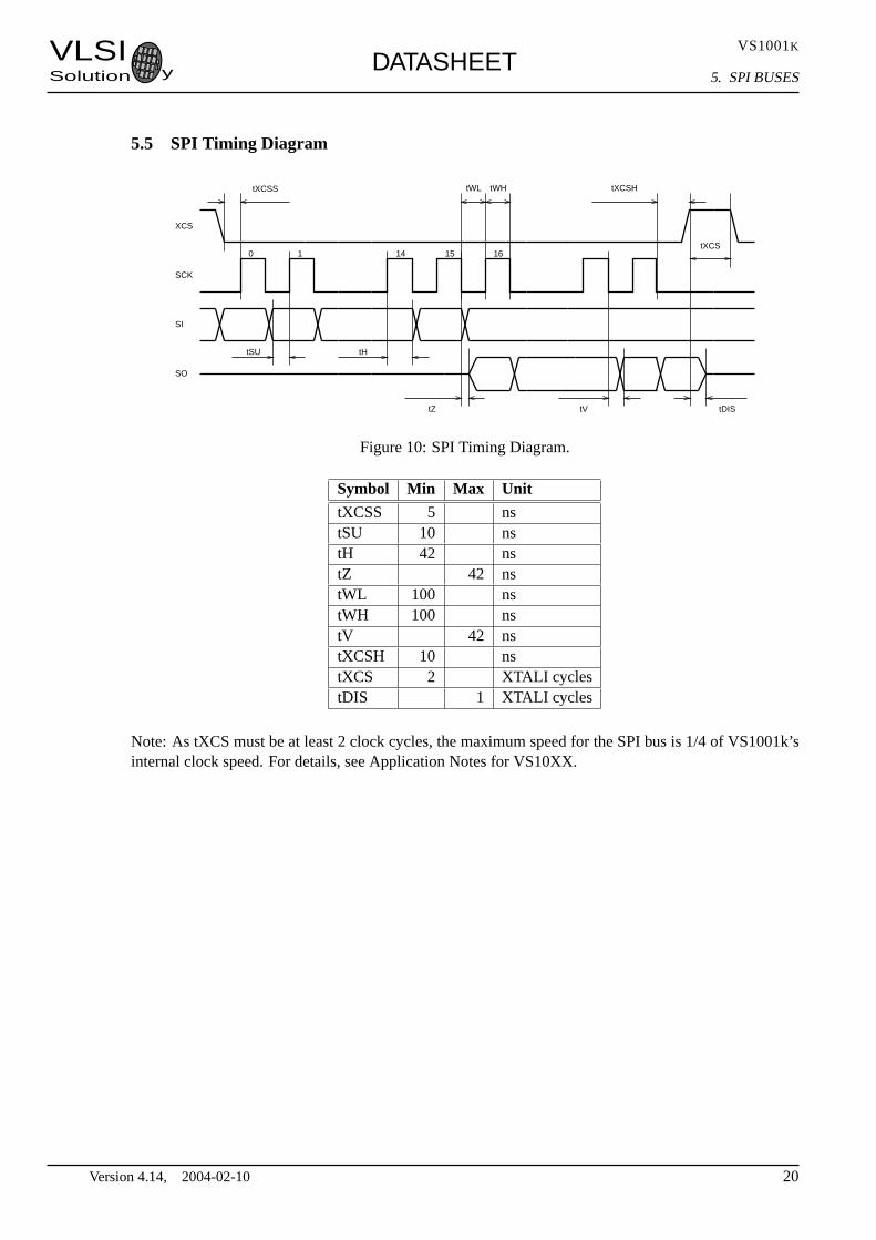
5.5 SPI Timing Diagram
XCS
SCK
SI
SO
0 1 1514 16
tXCSS tXCSHtWL tWH
tHtSU
tVtZ tDIS
tXCS
Figure 10: SPI Timing Diagram.
Symbol Min Max Unit
tXCSS 5 nstSU 10 nstH 42 nstZ 42 nstWL 100 nstWH 100 nstV 42 nstXCSH 10 nstXCS 2 XTALI cyclestDIS 1 XTALI cycles
Note: As tXCS must be at least 2 clock cycles, the maximum speed for the SPI bus is 1/4 of VS1001k’sinternal clock speed. For details, see Application Notes for VS10XX.
Version 4.14, 2004-02-10 20
VLSISolution y DATASHEET
VS1001K
6. FUNCTIONAL DESCRIPTION
6 Functional Description
6.1 Main Features
VS1001k is based on a proprietary digital signal processor, VSDSP. It contains all the code and datamemory needed for MPEG audio decoding, together with serial interfaces, a multirate stereo audio DACand analog output amplifiers and filters.
VS1001k can play all MPEG 1 and 2 layer 3 files, as well as so-called MPEG 2.5 layer 3 extensionfiles with all sample rates and bitrates. In addition, variable bitrate (VBR) is also supported. WithVBR, and depending on the song, near-cd quality can be achieved with approximately 100 kbits/s forstereo music sampled at 44100 Hz, whereas old encoders required 128 kbits/s for the same task. Asboth commercial and free (http://www.mp3dev.org/) high-quality VBR encoders are nowadays widelyavailable, MP3 format is getting better as it is maturing.
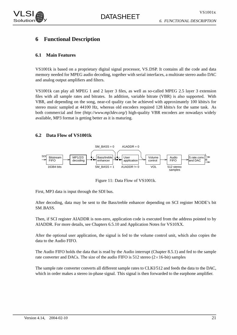
6.2 Data Flow of VS1001k
BitstreamFIFO
MP1/2/3decoding
Bass/trebleenhancer
Volumecontrol
AudioFIFO
S.rate.conv.and DAC
Userapplication R
SM_BASS = 0
SM_BASS = 1
A1ADDR = 0
A1ADDR != 016384 bits 512 stereo samples
SDI L
VOL
Figure 11: Data Flow of VS1001k.
First, MP3 data is input through the SDI bus.
After decoding, data may be sent to the Bass/treble enhancer depending on SCI register MODE’s bitSM BASS.
Then, if SCI register AIADDR is non-zero, application code is executed from the address pointed to byAIADDR. For more details, see Chapters 6.5.10 and Application Notes for VS10XX.
After the optional user application, the signal is fed to the volume control unit, which also copies thedata to the Audio FIFO.
The Audio FIFO holds the data that is read by the Audio interrupt (Chapter 8.5.1) and fed to the samplerate converter and DACs. The size of the audio FIFO is 512 stereo (2×16-bit) samples
The sample rate converter converts all different sample rates to CLKI/512 and feeds the data to the DAC,which in order makes a stereo in-phase signal. This signal is then forwarded to the earphone amplifier.
Version 4.14, 2004-02-10 21
VLSISolution y DATASHEET
VS1001K
6. FUNCTIONAL DESCRIPTION
6.3 Serial Data Interface (SDI)
The serial data interface is meant for transferring compressed MPEG audio data.
Also several different tests may be activated through SDI as described in Chapter 7.
6.4 Serial Control Interface (SCI)
The serial control interface is compatible with the SPI bus specification. Data transfers are always 16-bits. The VS1001k is controlled by writing and reading the registers of the interface.
The main controls of the control interface are:
• control of the operation mode• uploading user programs• access to header data• status information• access to decoded digital data• feeding input data
6.5 SCI Registers
Name Type addr FunctionMODE RW 0 mode controlSTATUS RW 1 status of VS1001kINT FCTLH - 2 internal register, never useCLOCKF RW 3 clock freq + doublerDECODETIME R 4 decode time in secondsAUDATA R 5 misc. audio dataWRAM W 6 RAM write programWRAMADDR W 7 base address for
RAM writeHDAT0 R 8 read header dataHDAT1 R 9 read header dataAIADDR RW 10 start address of
applicationVOL RW 11 volume controlRESERVED - 12 reserved for VS1002 use, don’t touchAICTRL[x] RW 13+x 2 application control
registers
x = [0 .. 1]
All registers are filled with zeros at hardware reset.
Version 4.14, 2004-02-10 22
VLSISolution y DATASHEET
VS1001K
6. FUNCTIONAL DESCRIPTION
6.5.1 MODE (RW)
MODE is used to control the operation of VS1001k.
Bit Name Function Value Description
0 SM DIFF differential 0 normal in-phase audio1 left channel inverted
1 SM FFWD fast forward 0 normal playback1 fast forward on
2 SM RESET soft reset 0 no reset1 reset
3 SM UNUSED1 set to 0 0 Set to 04 SM PDOWN powerdown 0 power on
1 powerdown5 SM UNUSED2 set to 0 0 Set to 06 SM UNUSED3 set to 0 0 Set to 07 SM BASS bass/treble enhancer 0 off
1 on8 SM DACT DCLK active 0 rising
edge 1 falling9 SM BITORD Byte order on serial input bus 0 MSB first
1 MSB last10 SM IBMODE input bus mode 0 slave
1 master11 SM IBCLK input bus clk when VS1001k is master 0 512 kHz
1 1024 kHz
When SMDIFF is set, the player inverts the left output. For a stereo input, this creates a virtual surround,and for a mono input this effectively creates a differential left/right signal.
By setting SMFFWD the player starts to accept SCI data at a high speed, and just decodes the audioheaders silently without playing any data. This can be used to fast-forward data with safe landing.Register DECODETIME is updated during a fast-forward just as normal.
By setting SMRESET to 1, the player is reset.
SM UNUSED1 should always be set to 0.
Bit SM PDOWN overrides any other: it turns VS1001k into powerdown mode, where the only opera-tional part is the control bus. (not implemented)
SM UNUSED2 and SMUNUSED3 should always be set to 0.
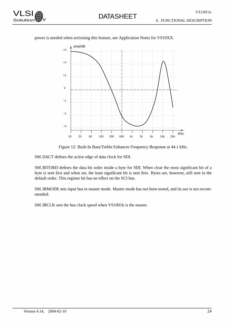
Bit SM BASS turns on the built-in Bass and Treble enhancer. The frequency response of the enhancerwhen the sample rate is 44.1 kHz is shown in Figure 12. For other sample frequencies the responsefrequence axis must be adjusted accordingly. Example: If the sample rate is 48 kHz, the 1 kHz frequencyin the figure is actually 1 kHz× 48 kHz / 44.1 kHz = 1.09 kHz. For details of how much extra processing
Version 4.14, 2004-02-10 23
VLSISolution y DATASHEET
VS1001K
6. FUNCTIONAL DESCRIPTION
power is needed when activating this feature, see Application Notes for VS10XX.
10 20 50 100 200 500 1k 2k 5k 10k 20k
+3
+2
+1
0
−1
−2
−3
ampl/dB
f/Hz
Figure 12: Built-In Bass/Treble Enhancer Frequency Response at 44.1 kHz.
SM DACT defines the active edge of data clock for SDI.
SM BITORD defines the data bit order inside a byte for SDI. When clear the most significant bit of abyte is sent first and when set, the least significant bit is sent first. Bytes are, however, still sent in thedefault order. This register bit has no effect on the SCI bus.
SM IBMODE sets input bus to master mode. Master mode has not been tested, and its use is not recom-mended.
SM IBCLK sets the bus clock speed when VS1001k is the master.
Version 4.14, 2004-02-10 24

VLSISolution y DATASHEET
VS1001K
6. FUNCTIONAL DESCRIPTION
6.5.2 STATUS (RW)
STATUS contains information on the current status of the VS1001k. Bits 1 and 0 are used to controlanalog output volume: 0 = -0 dB, 1 = -6 dB, 3 = -12 dB. Bit 2 is analog powerdown bit. When set to 1,analog is put to powerdown.
Note: writing to register VOL will automatically set the analog output volume, and muting if necessary.Thus, the user needn’t worry about this register.
6.5.3 INT FCNTLH (-)
INT FCTLH is not a user-accessible register.
6.5.4 CLOCKF (RW)
CLOCKF is used to tell if the input clock XTALI is running at something else than 24.576 MHz. XTALIis set in 2 kHz steps. Thus, the formula for calculating the correct value for this register isXTALI/2000(XTALI is in Hz). Values may be between 0..32767, although hardware limits the highest allowed speed.Also, with lower-than 24.576 MHz speeds all sample rates and bit-stream widths are no longer available.
Setting the MSB of CLOCKF to 1 activates internal clock-doubling. A clock of upto 15 MHz may bedoubled depending on the voltage provided to the chip.
Note: CLOCKF must be set before beginning decoding MP3 data; otherwise the sample rate will not beset correctly.
Example 1: For a 26 MHz clock the value would be26000000/2000 = 13000.
Example 2: For a 13 MHz external clock and using internal clock-doubling for a 26 MHz internalfrequency, the value would be0x8000 + (13000000/2000) = 39268.
Example 3: For a 24.576 MHz clock the value would be either24576000/2000 = 12288, or just thedefault value0. For this clock frequency, CLOCKF doesn’t need to be set at all.
6.5.5 DECODETIME (R)
When decoding correct data, current decoded time is shown in this register in full seconds.
Version 4.14, 2004-02-10 25
VLSISolution y DATASHEET
VS1001K
6. FUNCTIONAL DESCRIPTION
6.5.6 AUDATA (R)
When decoding correct data, the current bitrate in kbits/s can be found in bits 8..0 of AUDATA. For avariable bitrate bitstream, the current bitstream width is displayed. Bits 12..9 contains an index to thesample rate. The indices are shown in the table below. Bits 14..13 are not in use and always set to 0. Bit15 is 0 for mono data and 1 for stereo.
Bits 12..9 Sample Rate/Hz
0b0000 Unknown0b0001 441000b0010 480000b0011 320000b0100 220500b0101 240000b0110 160000b0111 110250b1000 120000b1001 8000
6.5.7 WRAM (W)
WRAM is used to upload application programs to program RAM. The start address must be initializedby writing to the WRAMADDR register prior to the first call of WRAM. value will be used. As 16 bits ofdata can be transferred with one WRAM write, and the program word is 32 bits, two consecutive writesare needed for each program word. The byte order is big-endian (i.e. MSBs first). After each full-wordwrite, the internal pointer is autoincremented.
6.5.8 WRAMADDR (W)
WRAMADDR is used to set the program address for following WRAM writes. User program space isbetween addresses 0x4000 .. 0x43ff (with addresses 0x4000 .. 0x401f being reserved by the system),but for writes through the WRAM mechanism, they are visible at addresses 0x4000 higher. Thus, if theprogrammer wish to write his application to address 0x4167, he should write 0x4167 + 0x4000 = 0x8167to WRAMADDR.
Version 4.14, 2004-02-10 26
VLSISolution y DATASHEET
VS1001K
6. FUNCTIONAL DESCRIPTION
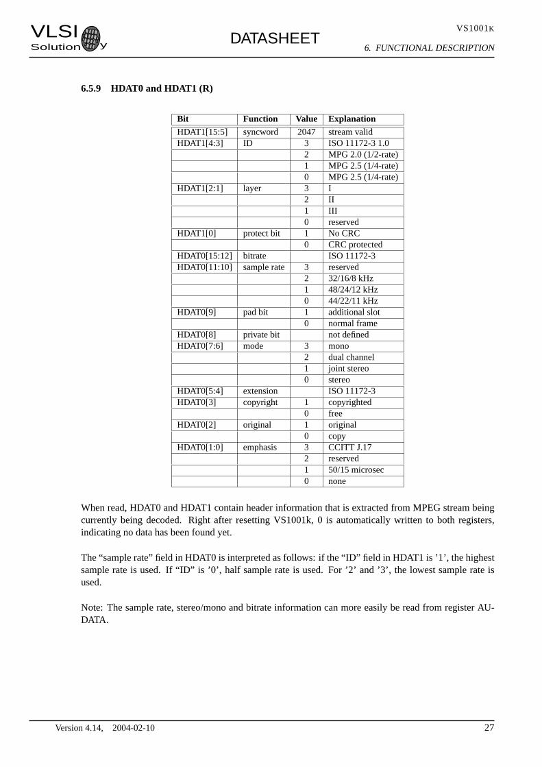
6.5.9 HDAT0 and HDAT1 (R)
Bit Function Value ExplanationHDAT1[15:5] syncword 2047 stream validHDAT1[4:3] ID 3 ISO 11172-3 1.0
2 MPG 2.0 (1/2-rate)1 MPG 2.5 (1/4-rate)0 MPG 2.5 (1/4-rate)
HDAT1[2:1] layer 3 I2 II1 III0 reserved
HDAT1[0] protect bit 1 No CRC0 CRC protected
HDAT0[15:12] bitrate ISO 11172-3HDAT0[11:10] sample rate 3 reserved
2 32/16/8 kHz1 48/24/12 kHz0 44/22/11 kHz
HDAT0[9] pad bit 1 additional slot0 normal frame
HDAT0[8] private bit not definedHDAT0[7:6] mode 3 mono
2 dual channel1 joint stereo0 stereo
HDAT0[5:4] extension ISO 11172-3HDAT0[3] copyright 1 copyrighted
0 freeHDAT0[2] original 1 original
0 copyHDAT0[1:0] emphasis 3 CCITT J.17
2 reserved1 50/15 microsec0 none
When read, HDAT0 and HDAT1 contain header information that is extracted from MPEG stream beingcurrently being decoded. Right after resetting VS1001k, 0 is automatically written to both registers,indicating no data has been found yet.
The “sample rate” field in HDAT0 is interpreted as follows: if the “ID” field in HDAT1 is ’1’, the highestsample rate is used. If “ID” is ’0’, half sample rate is used. For ’2’ and ’3’, the lowest sample rate isused.
Note: The sample rate, stereo/mono and bitrate information can more easily be read from register AU-DATA.
Version 4.14, 2004-02-10 27

VLSISolution y DATASHEET
VS1001K
6. FUNCTIONAL DESCRIPTION
6.5.10 AIADDR (RW)
AIADDR indicates the start address of the application code written earlier through WRAMADDR andWRAM registers. If no application code is used, this register should not be initialized, or it should beinitialized to zero. For more details, see Application Notes for VS10XX.
6.5.11 VOL (RW)
VOL is a volume control for the player hardware. For each channel, a value in the range of 0 .. 255may be defined to set its attenuation from the maximum volume level (in 0.5 dB steps). The left channelvalue is then multiplied by 256 and the values are added. Thus, maximum volume is 0 and total silence if65535. Example: for a volume of -2.0 dB for the left channel and -3.5 dB for the right channel: (4*256)+ 7 = 1031. Note, that at startup volume is set to full volume. Resetting the software does not reset thevolume setting.
Note: Setting the volume to total silence (255 for both left and right channels), will turn analog poweroff. This will save power, but also cause a slight snap in the earphones. If you want to turn the volumeoff but don’t want this snap, turn the volume only to 254 for both channels (0xFEFE).
6.5.12 RESERVED (RW)
This register has been reserved for future use.
6.5.13 AICTRL[x] (RW)
AICTRL[x] -registers ( x=[0 .. 1] ) can be used to access the user’s application program.
6.6 Stereo Audio DAC
The decoded digital data is transformed into analog format by an 18-bit oversampling multi-bit sigma-delta DA-converter. The oversampled output is low-pass filtered by an on-chip analog filter. The outputrate of the DA-converter is always 1/4 of the clock rate, or 128 times the highest usable sample rate. Forinstance for a 24.576 MHz clock, the DA-converter operates at 128x48 kHz, which is 6.144 MHz. If theinput sample rate is other than 48 kHz, it is internally converted to 48 kHz by the DAC. This removes theneed for complex PLL-based clocking schemes and still allows the use of several sample rates with onefixed master clock frequency.
The outputs can be separately muted by the user. If the output of the decoder is invalid or input data isnot received fast enough, analog outputs are automatically muted. The analog outputs have buffers thatare capable of driving 30Ω loads with a maximum of 50nF capacitance.
Version 4.14, 2004-02-10 28
VLSISolution y DATASHEET
VS1001K
7. OPERATION
7 Operation
7.1 Clocking
The VS1001k chip operates typically on a single 24.576 MHz fundamental frequency master clock. Thisclock can be generated by external circuitry (connected to pin XTALI) or by the internal clock chrystalinterface (pins XTALI and XTALO). This clock is sufficient to support a high quality audio output foralmost all the standard sample rates and bit-rates (see Application Notes for VS10XX).
Note: Oscillators above 24.576 MHz are usually so-called3rd harmonic clocks, which have a fundamen-tal frequency of 1/3 of the nominal clock frequency. With such an oscillator, VS1001 would be running atthe base frequency, if working at all. Thus, for instance, if you run VS1001 with a 32 MHz3rd harmonicclock, you usually end up running the chip at 32 MHz / 3 = 10.67 MHz.
7.2 Powerdown
In powerdown mode the chip only monitors the control bus. The analog output drivers are turned off andthe processor remains in hold-state.
7.3 Hardware Reset
When the XRESET -signal is driven low, VS1001k is reset and all the control registers and internalstates are set to the initial values. XRESET-signal is asynchronous to any external clock. The reset modedoubles as a full-powerdown mode, where both digital and analog parts of VS1001k are in minimumpower consumption stage, and where clocks are stopped. Also XTALO and XTALI are grounded.
After a hardware reset (or at power-up), set the basic software registers such as VOL for volume (andCLOCKF if the input clock is anything else than 24.576 MHz) before starting decoding.
7.4 Software Reset
Between any two MP3 files, the decoder software has to be reset. This is done by activating bit 2 in SCI’sMODE register (Chapter 6.5.1). Then wait for at least 2µs, then look at DREQ. DREQ will stay downfor at least 6000 clock cycles, which means an approximate 250µs delay if VS1001k is run at 24.576MHz. When DREQ goes up, write at least one zero to SDI. After this, you may continue playback asusual.
If you want to make sure VS1001k doesn’t cut the ending of low-bitrate data streams, it is recommendedto feed 2048 zeros to the SDI bus before activating the reset bit (DREQ must be respected just as withnormal SDI data). This will make sure all frames have been decoded before resetting the chip.
Version 4.14, 2004-02-10 29
VLSISolution y DATASHEET
VS1001K
7. OPERATION
7.5 Play/Decode
This is the normal operation mode of VS1001k. The SDI data is decoded. Decoded samples are convertedto analog domain by the internal DAC, If there are errors in the decoding process, the error flags of SCI’sHDAT0 and HDAT1 are set accordingly. In case there are serious errors in the input data, decoding isstill continued, but the analog outputs are muted.
When there is no valid input for decoding, VS1001k goes into idle mode (lower power consumption thanduring decoding) and actively monitors the serial data input for valid data. The data input does not needto be clocked (DCLK) when no data is sent.
The software needs to be reset between MPEG audio stream files. See for the Chapter “Testing” to seehow it is done.
7.6 Sanity Checks
Although VS1001k checks extensively for bad MP3 streams, it may happen that it encounters a bitstreamthat makes the firmware’s recovery code fail. This may particularly happen during fast forward and fastbackwards operations, where the data where the microcontroller lands the MP3 decoder may not be avalid header.
The microcontroller should keep a look at the data speeds VS1001k requires. If data input either stopscompletely (DREQ always inactive) for a whole second, or if VS1001k requires more than 60 KiB datain any single second, it is the responsibility of the microcontroller to either reset the software. If thatdoesn’t help, a hardware reset should be issued.
7.7 PCM Mode
VS1001k can be used as a Digital-to-Analog converter (DAC) by feeding PCM data. A convenient wayto use VS1001k as a DAC is to loadSDI PCM Extension for VS1001ksoftware from VLSI Solution’shome page athttp://www.vlsi.fi/vs1001/software/.
The SDI PCM Extension makes it possible for the user to use SDI to feed 8-bit or 16-bit PCM samplesin mono or stereo at any sample rate upto 48 kHz (with nominal 24.576 MHz operating frequency).
7.8 Testing
There are several test modes in VS1001k, which allow the user to perform memory tests, SCI bus tests,and several different sine wave tests ranging from 250 Hz to 1500 Hz.
All tests are started in a similar way: VS1001 is hardware reset, and then a test command is sent to theSDI bus. Each test is started by sending a 4-byte special command sequence, followed by 4 zeros. Thesequences are described below.
Version 4.14, 2004-02-10 30
VLSISolution y DATASHEET
VS1001K
7. OPERATION
7.8.1 Memory Test
Memory test mode is initialized with the 8-byte sequence 0x4D 0xEA 0x6D 0x54 0 0 0 0. After thiscommand (and its required 4 zeros), wait for 500000 clock cycles. The result can be read from the SCIregister HDAT0, and ’one’ bits are interpreted as follows:
Bit(s) Meaning
0 Good X ROM1 Good Y ROM (high)2 Good Y ROM (low)3 Good Y RAM4 Good X RAM5 Good Instruction RAM (high)6 Good Instruction RAM (low)7 Unused
All tests are non-destructive and interrupts are disabled during testing. Thus, no user software or data isharmed by the tests.
Instruction ROM cannot be tested with software.
7.8.2 SCI Test
Sci test is initialized with the 8-byte sequence 0x53 0x70 0xEEn 0 0 0 0, wheren − 48 is the registernumber to test. The content of the given register is read and copied to HDAT0. If the register to be testedis HDAT0, the result is copied to HDAT1.
Example: ifn is 48, contents of SCI register 0 (MODE) is copied to HDAT0.
Version 4.14, 2004-02-10 31
VLSISolution y DATASHEET
VS1001K
7. OPERATION
7.8.3 Sine Test
Sine test is initialized with the 8-byte sequence: 0x53 0xEF 0x6En 0 0 0 0, wheren (48..119) definesthe sine test to use. If we defineFsIdx = (n− 48)mod9 andFSin = (n− 48)/9, the following tablesmay be used:
FsIdx Fs
0 44100 Hz1 48000 Hz2 32000 Hz3 22050 Hz4 24000 Hz5 16000 Hz6 11025 Hz7 12000 Hz8 8000 Hz
FSin Length of Sin
0 32.000 samples1 16.000 samples2 10.667 samples3 8.000 samples4 6.400 samples5 5.333 samples6 4.571 samples7 4.000 samples
Example: Sine test is called with a test value of 62. 62-48 = 14, FsIdx = 5 and FSin = 1. From the tableswe get the sample rate 16000 Hz, and the sine wave length, which is 16 samples. Thus, we’ll get a 1 kHzvoice.
To exit the sine test, send the sequence 0x45 0x78 0x69 0x74 0 0 0 0.
Note: The sine test signals go through the digital volume control, so it is possible to test channelsseparately.
Version 4.14, 2004-02-10 32
VLSISolution y DATASHEET
VS1001K
8. WRITING SOFTWARE
8 Writing Software
8.1 When to Write Software
User software is required when a user wishes to add some own functionality like DSP effects or tonecontrols to VS1001k. Some tone controls are available from VLSI Solution, but if a user wishes to gofurther than that or use VS1001k in some unexpected way, this is how to do it.
However, most of the users of VS1001k don’t need to worry about writing their own code, or this chapter.
8.2 The Processor Core
VS DSP is a 16/32-bit DSP processor core that can very well also be used as an all-purpose processor.The VLSI Solution’s free VSKIT Software Package contains all the tools and documentation needed towrite, simulate and debug Assembly Language or Extended ANSI C programs for the VSDSP processorcore.
The VSKIT Software Package is available on request from VLSI Solution.
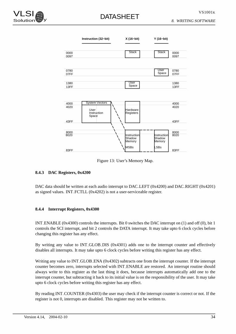
8.3 User’s Memory Map
User’s Memory Map is shown in Figure 13.
8.4 Hardware Registers
All hardware registers are located in X memory.
8.4.1 SCI Registers, 0x4000
All SCI registers described in Chapter 6.5 can be found here between 0x4000..0x40FF.
8.4.2 Serial Registers, 0x4100
SERDATA (0x4100) contains the last data value read from the data bus. The LSB of SERDREQ(0x4101) defines the status of the DREQ signal.
Version 4.14, 2004-02-10 33
VLSISolution y DATASHEET
VS1001K
8. WRITING SOFTWARE
00000097
00000097
Stack Stack
Instruction (32−bit) Y (16−bit)X (16−bit)
40004020
43FF
8000
83FF
40004020
43FF
8000
83FF
UserSpace
System Vectors
80208020 InstructionShadowMemory
MSBs
InstructionShadowMemory
LSBs
HardwareRegisters
UserInstructionSpace
078007FF
138013FF
078007FF
138013FF
UserSpace
Figure 13: User’s Memory Map.
8.4.3 DAC Registers, 0x4200
DAC data should be written at each audio interrupt to DACLEFT (0x4200) and DACRIGHT (0x4201)as signed values. INTFCTLL (0x4202) is not a user-serviceable register.
8.4.4 Interrupt Registers, 0x4300
INT ENABLE (0x4300) controls the interrupts. Bit 0 switches the DAC interrupt on (1) and off (0), bit 1controls the SCI interrupt, and bit 2 controls the DATA interrupt. It may take upto 6 clock cycles beforechanging this register has any effect.
By writing any value to INTGLOB DIS (0x4301) adds one to the interrupt counter and effectivelydisables all interrupts. It may take upto 6 clock cycles before writing this register has any effect.
Writing any value to INTGLOB ENA (0x4302) subtracts one from the interrupt counter. If the interruptcounter becomes zero, interrupts selected with INTENABLE are restored. An interrupt routine shouldalways write to this register as the last thing it does, because interrupts automatically add one to theinterrupt counter, but subtracting it back to its initial value is on the responsibility of the user. It may takeupto 6 clock cycles before writing this register has any effect.
By reading INTCOUNTER (0x4303) the user may check if the interrupt counter is correct or not. If theregister is not 0, interrupts are disabled. This register may not be written to.
Version 4.14, 2004-02-10 34
VLSISolution y DATASHEET
VS1001K
8. WRITING SOFTWARE
8.5 System Vector Tags
The System Vector Tags are tags that may be replaced by the user to take control over several decoderfunctions.
8.5.1 AudioInt, 0x4000..0x4001
Normally contains the following VSDSP assembly code:
j dac_intstx mr1,(i6)+1 ; sty i7,(i6)
The user may, at will, replace the first instruction with either aj or jmpi command to gain control overthe audio interrupt. It is not recommended to change the instruction at 0x4001.
8.5.2 SpiInt, 0x4002..0x4003
Normally contains the following VSDSP assembly code:
j spi_intstx mr1,(i6)+1 ; sty i7,(i6)
The user may, at will, replace the first address with either a j or jmpi command to gain control over theSCI interrupt. It is not recommended to change the instruction at 0x4003.
8.5.3 DataInt, 0x4004..0x4005
Normally contains the following VSDSP assembly code:
j data_intstx mr1,(i6)+1 ; sty i7,(i6)
The user may, at will, replace the first address with either a j or jmpi command to gain control over theMP3 data interrupt. It is not recommended to change the instruction at 0x4005.
8.5.4 UserCodec, 0x4008..0x4009
Normally contains the following VSDSP assembly code:
jrnop
Version 4.14, 2004-02-10 35

VLSISolution y DATASHEET
VS1001K
8. WRITING SOFTWARE
If the user wants to take control away from the standard decoder, the first instruction should be replacedwith an appropriate jump command to user’s own code.
Unless the user is feeding MP3 data at the same time, the system activates the user program in less than1 ms. After this, the user should steal interrupt vectors from the system, and then insert user programs.
8.6 System Vector Functions
The System Vector Functions are pointers to some functions that the user may call to help implementinghis own applications.
8.6.1 WriteIRam(), 0x4010
VS DSP C prototype:
void WriteIRam(register i0 u int16 *addr, register a1 u int16 msW, register a0 u int16 lsW);
This is the only supported way to write to the User Instruction RAM. This is because Instruction RAMcannot be written when program control is in RAM. Thus, the actual implementation of this function isin ROM, and here is simply a tag to that routine.
Note: Instruction RAM is shadowed 0x4000 addresses higher in the X and Y RAMs. Thus, if you wantto write to instruction address 0x4020,addr must be 0x4020 + 0x4000 = 0x8020.
8.6.2 ReadIRam(), 0x4011
VS DSP C prototype:
u int32 ReadIRam(registeri0 u int16 *addr);
This is the only supported way to read from the User Instruction RAM. This is because Instruction RAMcannot be read when program control is in RAM. Thus, the actual implementation of this function is inROM, and here is simply a tag to that routine.
A1 contains the MSBs and a0 the LSBs of the result.
Note: Instruction RAM is shadowed 0x4000 addresses higher in the X and Y RAMs. Thus, if you wantto read from instruction address 0x4020,addr must be 0x4020 + 0x4000 = 0x8020.
Version 4.14, 2004-02-10 36
VLSISolution y DATASHEET
VS1001K
8. WRITING SOFTWARE
8.6.3 DataWords(), 0x4012
VS DSP C prototype:
u int16 DataWords(void);
If the user has taken over the normal operation of the system by switching the pointer in UserCodecto point to his own code, he may read data from the Data Interface through this and the following twofunctions. This function returns the number of data words (each containing two bytes of data) that can beread. If there is not enough data available, data acquisition functions GetDataByte() and GetDataWords()may NOT be called!
8.6.4 GetDataByte(), 0x4013
VS DSP C prototype:
u int16 GetDataByte(void);
Reads and returns one data byte from the Data Interface.
Before calling this function, always check first that there are at least 1 word waiting with function Data-Words().
8.6.5 GetDataWords(), 0x4014
VS DSP C prototype:
void GetDataWords(registeri0 y u int16 *d, register a0 u int16 n);
Readn data byte pairs and copy them in big-endian format (first byte to MSBs) tod.
Before calling this function, always check first that there are at least 1+n words waiting with functionDataWords().
Version 4.14, 2004-02-10 37
VLSISolution y DATASHEET
VS1001K
9. VS1001 VERSION CHANGES
9 VS1001 Version Changes
This chapter describes changes between different generations of VS1001.
Note: VS1001k is the final, production version of VS1001.
9.1 Changes Between VS1001h and Production Version VS1001k, 2001-08
• When the chip is reset with pin XRESET, XTALO and XTALI are driven to ground.
• Running with normal clock earlier required slightly different clock generation than for clock-doubled (see Chapters 4.1 and 4.2). This is no longer the case.
• Lots of new SCI register MODE bits: SMDIFF, SM FFWD, SM BASS. For details, see Chap-ter 6.5.1.
• Default is now to only decode MP3.
• 20..60 mV DAC offset corrected.
• A firmware bug made it impossible to decode 320 kbits/s MP3 data. This has been corrected.
• A hardware bug made it practically impossible to load code to RAM. This has been corrected.
9.2 Changes Between VS1001g and VS1001h, 2001-05
• Analog voltage requirements have been lowered. Now full gain can be achieved with a 2.7 Vanalog input voltage, whereas 3.4 V was needed before.
9.3 Changes Between VS1001d to VS1001g, 2001-03
• Clock is now adjustable, in VS1001d only 24.576 MHz could be used.
• Clock doubler added.
• VS1001d played 48 kHz instead of 12 or 24 kHz, this is corrected.
Version 4.14, 2004-02-10 38

VLSISolution y DATASHEET
VS1001K
10. DOCUMENT VERSION CHANGES
10 Document Version Changes
This chapter describes the most important changes to this document.
10.1 Changes Between Version 4.13 and 4.14 for VS1001k, 2004-02
• New pin names for pins 41 (GBGND) and 43 (GBVDD) in LQFP-48 Pin Description, Chap-ter 6.5.1.
• Renamed SMBYTEORD to SMBITORD, see Chapter 3.3.
10.2 Changes Between Version 4.12 and 4.13 for VS1001k, 2003-11
• Changed pin 42 (VCM) to GBUF in Chapter 3.3.
• Added example connection diagram for LQFP-48, Chapter 4.3.
10.3 Changes Between Version 4.11 and 4.12 for VS1001k, 2003-10
• In Chapter 3.3, TEST1 and TEST2 were told to be connected to pin 32 in LQFP-48 packaging,now corrected to pins 33 and 34, respectively.
10.4 Changes Between Version 4.10 and 4.11 for VS1001k, 2003-09
• Minor modifications to front page.
• Moved all Application Notes to a separate document, VS10XX Application Notes.
10.5 Changes Between Version 4.08 and 4.10 for VS1001k, 2003-07
• Added LQFP-48 packaging, Chapter 3.3.
• Removed package figure for BGA-49 and provided an URL instead.
10.6 Changes Between Version 4.07 and 4.08 for VS1001k, 2003-03
• Removed MP1 and MP2 functionality due to firmware problems.
• Removed Chapter Errata.
Version 4.14, 2004-02-10 39
VLSISolution y DATASHEET
VS1001K
11. CONTACT INFORMATION
11 Contact Information
VLSI Solution OyHermiankatu 6-8 CFIN-33720 Tampere
FINLAND
Fax: +358-3-316 5220Phone: +358-3-316 5230
Email: [email protected]: http://www.vlsi.fi/
Note: If you have questions, first seehttp://www.vlsi.fi/vs1001/faq/.
Version 4.14, 2004-02-10 40