Cyclone V Device DatasheetCyclone V Device Datasheet This datasheet describes the electrical...
48
June 2012 Altera Corporation CV-51002-2.0 Datasheet © 2012 Altera Corporation. All rights reserved. ALTERA, ARRIA, CYCLONE, HARDCOPY, MAX, MEGACORE, NIOS, QUARTUS and STRATIX words and logos are trademarks of Altera Corporation and registered in the U.S. Patent and Trademark Office and in other countries. All other words and logos identified as trademarks or service marks are the property of their respective holders as described at www.altera.com/common/legal.html. Altera warrants performance of its semiconductor products to current specifications in accordance with Altera's standard warranty, but reserves the right to make changes to any products and services at any time without notice. Altera assumes no responsibility or liability arising out of the application or use of any information, product, or service described herein except as expressly agreed to in writing by Altera. Altera customers are advised to obtain the latest version of device specifications before relying on any published information and before placing orders for products or services. 101 Innovation Drive San Jose, CA 95134 www.altera.com Feedback Subscribe ISO 9001:2008 Registered Cyclone V Device Datasheet This datasheet describes the electrical characteristics, switching characteristics, configuration specifications, and I/O timing for Cyclone ® V devices. Cyclone V devices are offered in commercial and industrial grades. Commercial devices are offered in –C6 (fastest), –C7, and –C8 speed grades. Industrial devices are offered in the –I7 speed grade. Automotive devices are offered in the –A7 speed grade. f For more information about the densities and packages of devices in the Cyclone V family, refer to the Cyclone V Device Overview . Electrical Characteristics The following sections describe the electrical characteristics of Cyclone V devices. Operating Conditions Cyclone V devices are rated according to a set of defined parameters. To maintain the highest possible performance and reliability of the Cyclone V devices, you must consider the operating requirements described in this datasheet. June 2012 CV-51002-2.0
Transcript of Cyclone V Device DatasheetCyclone V Device Datasheet This datasheet describes the electrical...

June 2012 Altera Corporation
CV-51002-2.0
© 2012 Altera Corporation. AlQUARTUS and STRATIX worOffice and in other countries. respective holders as describedproducts to current specificatioproducts and services at any tiof any information, product, oadvised to obtain the latest verfor products or services.
101 Innovation DriveSan Jose, CA 95134www.altera.com
June 2012CV-51002-2.0
Cyclone V Device Datasheet
Datasheet
This datasheet describes the electrical characteristics, switching characteristics, configuration specifications, and I/O timing for Cyclone® V devices.
Cyclone V devices are offered in commercial and industrial grades. Commercial devices are offered in –C6 (fastest), –C7, and –C8 speed grades. Industrial devices are offered in the –I7 speed grade. Automotive devices are offered in the –A7 speed grade.
f For more information about the densities and packages of devices in the Cyclone V family, refer to the Cyclone V Device Overview.
Electrical CharacteristicsThe following sections describe the electrical characteristics of Cyclone V devices.
Operating ConditionsCyclone V devices are rated according to a set of defined parameters. To maintain the highest possible performance and reliability of the Cyclone V devices, you must consider the operating requirements described in this datasheet.
l rights reserved. ALTERA, ARRIA, CYCLONE, HARDCOPY, MAX, MEGACORE, NIOS, ds and logos are trademarks of Altera Corporation and registered in the U.S. Patent and Trademark All other words and logos identified as trademarks or service marks are the property of their
at www.altera.com/common/legal.html. Altera warrants performance of its semiconductor ns in accordance with Altera's standard warranty, but reserves the right to make changes to any
me without notice. Altera assumes no responsibility or liability arising out of the application or use r service described herein except as expressly agreed to in writing by Altera. Altera customers are sion of device specifications before relying on any published information and before placing orders
Feedback Subscribe
ISO 9001:2008 Registered

Page 2 Electrical Characteristics
Absolute Maximum RatingsAbsolute maximum ratings define the maximum operating conditions for Cyclone V devices. The values are based on experiments conducted with the devices and theoretical modeling of breakdown and damage mechanisms.
The functional operation of the device is not implied for these conditions.
c Conditions other than those listed in Table 1 may cause permanent damage to the device. Additionally, device operation at the absolute maximum ratings for extended periods of time may have adverse effects on the device.
Table 1 lists the Cyclone V absolute maximum ratings.
Table 1. Absolute Maximum Ratings for Cyclone V Devices—Preliminary
Symbol Description Minimum Maximum Unit
VCC Core voltage and periphery circuitry power supply –0.5 1.35 V
VCCPGM Configuration pins power supply –0.5 3.75 V
VCC_AUX Auxiliary supply –0.5 3.75 V
VCCBAT Battery back-up power supply for design security volatile key register –0.5 3.75 V
VCCPD I/O pre-driver power supply –0.5 3.75 V
VCCIO I/O power supply –0.5 3.9 V
VCCA_FPLL PLL analog power supply –0.5 3.75 V
VCCH_GXB Transceiver high voltage power –0.5 3.75 V
VCCE_GXB Transceiver power –0.5 1.21 V
VCCL_GXB Clock network power –0.5 1.21 V
VI DC input voltage –0.5 4 V
VCC_HPS Core voltage power supply –0.5 1.35 V
VCCPD_HPS I/O pre-driver power supply –0.5 3.75 V
VCCIO_HPS I/O power supply –0.5 3.9 V
VCCRSTCLK_HPS Configuration pins power supply –0.5 3.75 V
VCCPLL_HPS PLL analog power supply –0.5 3.75 V
IOUT DC output current per pin –25 40 mA
TJ Operating junction temperature –55 125 °C
TSTG Storage temperature (No bias) –65 150 °C
Cyclone V Device Datasheet June 2012 Altera Corporation

Electrical Characteristics Page 3
Maximum Allowed Overshoot and Undershoot Voltage
During transitions, input signals may overshoot to the voltage listed in Table 2 and undershoot to -2.0 V for input currents less than 100 mA and periods shorter than 20 ns.
The maximum allowed overshoot duration is specified as a percentage of high time over the lifetime of the device. A DC signal is equivalent to 100% duty cycle.
For example, a signal that overshoots to 3.95 V can only be at 3.95 V for ~5% over the lifetime of the device; for a device lifetime of 10 years, this amounts to half a year.
Table 2 lists the maximum allowed input overshoot voltage and the duration of the overshoot voltage as a percentage of device lifetime.
Table 2. Maximum Allowed Overshoot During Transitions for Cyclone V Devices—Preliminary
Symbol Description Condition (V) Overshoot Duration as % of High Time Unit
Vi (AC) AC input voltage
3.7 100 %
3.75 59.79 %
3.8 33.08 %
3.85 18.45 %
3.9 10.36 %
3.95 5.87 %
4 3.34 %
4.05 1.92 %
4.1 1.11 %
June 2012 Altera Corporation Cyclone V Device Datasheet

Page 4 Electrical Characteristics
u Unit
V
V
V
V
V
V
V
V
V
V
V
V
V
V
V
V
V
V
V
V
V
°C
°C
°C
s —
—
R) circuitry
Recommended Operating ConditionsRecommended operating conditions are the functional operation limits for the AC and DC parameters for Cyclone V devices.
Table 3 lists the steady-state voltage values expected from Cyclone V devices. Power supply ramps must all be strictly monotonic, without plateaus.
Table 3. Recommended Operating Conditions for Cyclone V Devices—Preliminary
Symbol Description Condition Minimum Typical Maximm
VCC
Core voltage, periphery circuitry power supply, transceiver physical coding sublayer (PCS) power supply, and transceiver PCI Express® (PCIe®) hard IP digital power supply
— 1.07 1.1 1.13
VCC_AUX Auxiliary supply — 2.375 2.5 2.625
VCCPD(1)
I/O pre-driver (3.3 V) power supply — 3.135 3.3 3.465
I/O pre-driver (3.0 V) power supply — 2.85 3.0 3.15
I/O pre-driver (2.5 V) power supply — 2.375 2.5 2.625
VCCIO
I/O buffers (3.3 V) power supply — 3.135 3.3 3.465
I/O buffers (3.0 V) power supply — 2.85 3.0 3.15
I/O buffers (2.5 V) power supply — 2.375 2.5 2.625
I/O buffers (1.8 V) power supply — 1.71 1.8 1.89
I/O buffers (1.5 V) power supply — 1.425 1.5 1.575
I/O buffers (1.35 V) power supply — 1.283 1.35 1.418
I/O buffers (1.25 V) power supply — 1.19 1.25 1.31
I/O buffers (1.2 V) power supply — 1.14 1.2 1.26
VCCPGM
Configuration pins (3.3 V) power supply — 3.135 3.3 3.465
Configuration pins (3.0 V) power supply — 2.85 3.0 3.15
Configuration pins (2.5 V) power supply — 2.375 2.5 2.625
Configuration pins (1.8 V) power supply — 1.71 1.8 1.89
VCCA_FPLL(2) PLL analog voltage regulator power supply — 2.375 2.5 2.625
VCCBAT (3) Battery back-up power supply (For design security volatile key register) — 1.2 — 3.0
VI DC input voltage — –0.5 — 3.6
VO Output voltage — 0 — VCCIO
TJ Operating junction temperature
Commercial 0 — 85
Industrial –40 — 100
Automotive –40 — 125
tRAMP Power supply ramp timeStandard POR 200 µs — 100 m
Fast POR 200 µs — 4 ms
Notes to Table 3:
(1) VCCPD must be 2.5 V when VCCIO is 2.5, 1.8, 1.5, 1.35, 1.25 or 1.2 V. VCCPD must be 3.0 V when VCCIO is 3.0 V.(2) PLL digital voltage is regulated from VCCA_FPLL.(3) If you do not use the design security feature in Cyclone V devices, connect VCCBAT to a 1.5-V, 2.5-V, or 3.0-V power supply. The power-on reset (PO
monitors VCCBAT. Cyclone V devices do not exit POR if VCCBAT stays low.
Cyclone V Device Datasheet June 2012 Altera Corporation
Electrical Characteristics Page 5
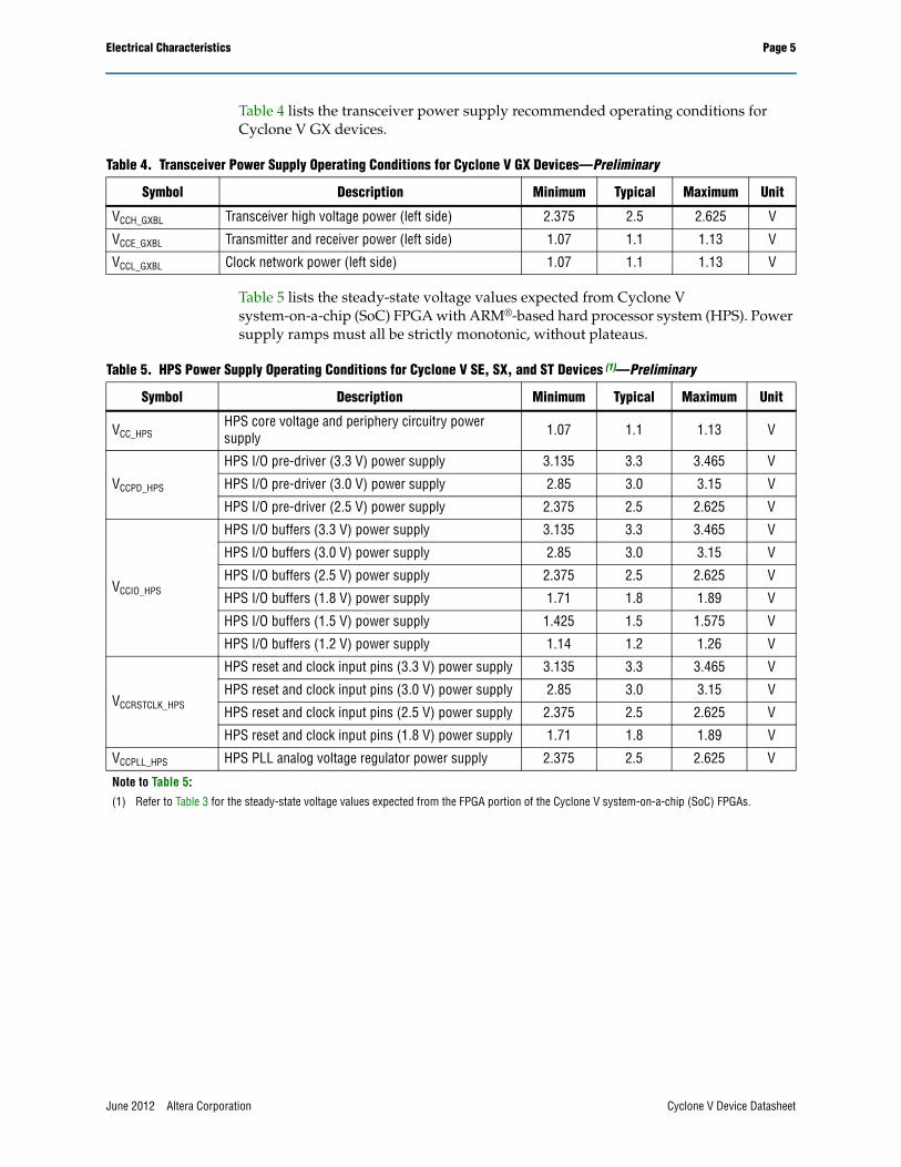
Table 4 lists the transceiver power supply recommended operating conditions for Cyclone V GX devices.
Table 5 lists the steady-state voltage values expected from Cyclone V system-on-a-chip (SoC) FPGA with ARM®-based hard processor system (HPS). Power supply ramps must all be strictly monotonic, without plateaus.
Table 4. Transceiver Power Supply Operating Conditions for Cyclone V GX Devices—Preliminary
Symbol Description Minimum Typical Maximum Unit
VCCH_GXBL Transceiver high voltage power (left side) 2.375 2.5 2.625 V
VCCE_GXBL Transmitter and receiver power (left side) 1.07 1.1 1.13 V
VCCL_GXBL Clock network power (left side) 1.07 1.1 1.13 V
Table 5. HPS Power Supply Operating Conditions for Cyclone V SE, SX, and ST Devices (1)—Preliminary
Symbol Description Minimum Typical Maximum Unit
VCC_HPSHPS core voltage and periphery circuitry power supply 1.07 1.1 1.13 V
VCCPD_HPS
HPS I/O pre-driver (3.3 V) power supply 3.135 3.3 3.465 V
HPS I/O pre-driver (3.0 V) power supply 2.85 3.0 3.15 V
HPS I/O pre-driver (2.5 V) power supply 2.375 2.5 2.625 V
VCCIO_HPS
HPS I/O buffers (3.3 V) power supply 3.135 3.3 3.465 V
HPS I/O buffers (3.0 V) power supply 2.85 3.0 3.15 V
HPS I/O buffers (2.5 V) power supply 2.375 2.5 2.625 V
HPS I/O buffers (1.8 V) power supply 1.71 1.8 1.89 V
HPS I/O buffers (1.5 V) power supply 1.425 1.5 1.575 V
HPS I/O buffers (1.2 V) power supply 1.14 1.2 1.26 V
VCCRSTCLK_HPS
HPS reset and clock input pins (3.3 V) power supply 3.135 3.3 3.465 V
HPS reset and clock input pins (3.0 V) power supply 2.85 3.0 3.15 V
HPS reset and clock input pins (2.5 V) power supply 2.375 2.5 2.625 V
HPS reset and clock input pins (1.8 V) power supply 1.71 1.8 1.89 V
VCCPLL_HPS HPS PLL analog voltage regulator power supply 2.375 2.5 2.625 V
Note to Table 5:
(1) Refer to Table 3 for the steady-state voltage values expected from the FPGA portion of the Cyclone V system-on-a-chip (SoC) FPGAs.
June 2012 Altera Corporation Cyclone V Device Datasheet

Page 6 Electrical Characteristics
DC CharacteristicsThis section lists the following specifications:
■ Supply Current and Power Consumption
■ I/O Pin Leakage Current
■ Bus Hold Specifications
■ OCT Specifications
■ Pin Capacitance
■ Hot Socketing
Supply Current and Power Consumption
Standby current is the current drawn from the respective power rails used for power budgeting.
Altera offers two ways to estimate power for your design—the Excel-based Early Power Estimator (EPE) and the Quartus® II PowerPlay Power Analyzer feature.
Use the Excel-based Early Power Estimator (EPE) before you start your design to estimate the supply current for your design. The EPE provides a magnitude estimate of the device power because these currents vary greatly with the resources you use.
The Quartus II PowerPlay Power Analyzer provides better quality estimates based on the specifics of the design after you complete place-and-route. The PowerPlay Power Analyzer can apply a combination of user-entered, simulation-derived, and estimated signal activities that, when combined with detailed circuit models, yields very accurate power estimates.
f For more information about power estimation tools, refer to the PowerPlay Early Power Estimator User Guide and the PowerPlay Power Analysis chapter in the Quartus II Handbook.
I/O Pin Leakage Current
Table 6 lists the Cyclone V I/O pin leakage current specifications.
Table 6. I/O Pin Leakage Current for Cyclone V Devices—Preliminary
Symbol Description Conditions Min Typ Max Unit
II Input pin VI = 0 V to VCCIOMAX –30 — 30 µA
IOZ Tri-stated I/O pin VO = 0 V to VCCIOMAX –30 — 30 µA
Cyclone V Device Datasheet June 2012 Altera Corporation

Electrical Characteristics Page 7
Bus Hold Specifications
Table 7 lists the Cyclone V device bus hold specifications.
Table 7. Bus Hold Parameters for Cyclone V Devices (1)—Preliminary
Parameter Symbol Conditions
VCCIO (V)
Unit1.2 1.5 1.8 2.5 3.0 3.3
Min Max Min Max Min Max Min Max Min Max Min Max
Bus-hold, low, sustaining current
ISUSLVIN > VIL
(max.)8 — 12 — 30 — 50 — 70 — 70 — µA
Bus-hold, high, sustaining current
ISUSHVIN < VIH
(min.)–8 — –12 — –30 — –50 — –70 — –70 — µA
Bus-hold, low, overdrive current
IODL0V < VIN <
VCCIO— 125 — 175 — 200 — 300 — 500 — 500 µA
Bus-hold, high, overdrive current
IODH0V < VIN <
VCCIO— –125 — –175 — –200 — –300 — –500 — –500 µA
Bus-hold trip point VTRIP — 0.3 0.9 0.375 1.125 0.68 1.07 0.7 1.7 0.8 2 0.8 2 V
Note to Table 7:
(1) The bus-hold trip points are based on calculated input voltages from the JEDEC standard.
June 2012 Altera Corporation Cyclone V Device Datasheet
Page 8 Electrical Characteristics
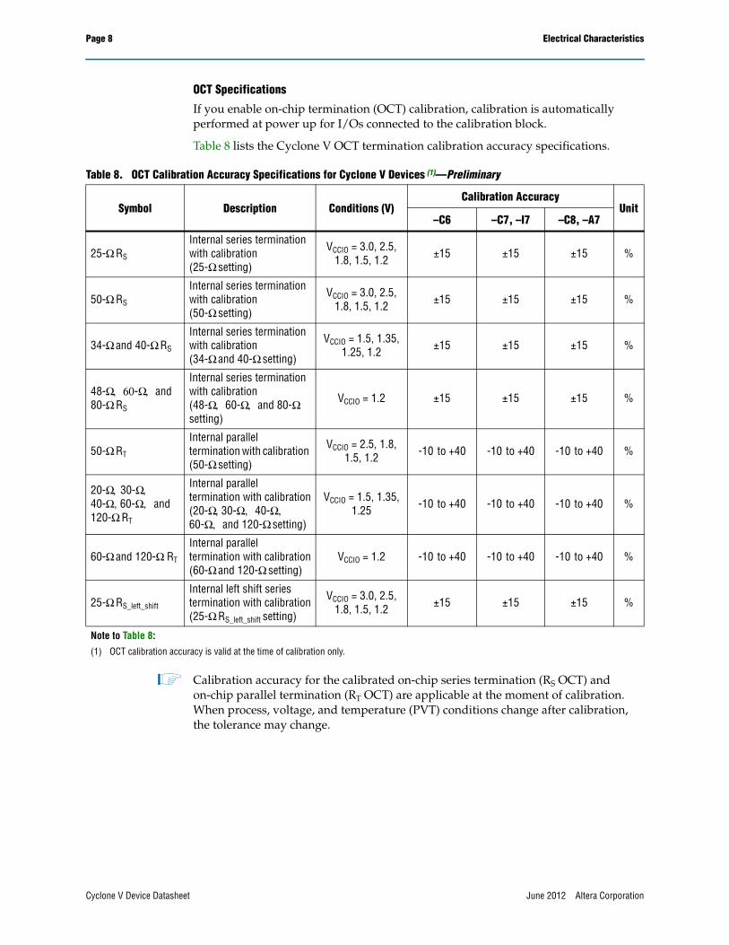
OCT Specifications
If you enable on-chip termination (OCT) calibration, calibration is automatically performed at power up for I/Os connected to the calibration block.
Table 8 lists the Cyclone V OCT termination calibration accuracy specifications.
1 Calibration accuracy for the calibrated on-chip series termination (RS OCT) and on-chip parallel termination (RT OCT) are applicable at the moment of calibration. When process, voltage, and temperature (PVT) conditions change after calibration, the tolerance may change.
Table 8. OCT Calibration Accuracy Specifications for Cyclone V Devices (1)—Preliminary
Symbol Description Conditions (V)Calibration Accuracy
Unit–C6 –C7, –I7 –C8, –A7
25-Ω RS Internal series termination with calibration(25-Ω setting)
VCCIO = 3.0, 2.5, 1.8, 1.5, 1.2 ±15 ±15 ±15 %
50-Ω RS Internal series termination with calibration (50-Ω setting)
VCCIO = 3.0, 2.5, 1.8, 1.5, 1.2 ±15 ±15 ±15 %
34-Ω and 40-Ω RS
Internal series termination with calibration(34-Ω and 40-Ω setting)
VCCIO = 1.5, 1.35, 1.25, 1.2 ±15 ±15 ±15 %
48-Ω, 60-Ω, and 80-Ω RS
Internal series termination with calibration(48-Ω, 60-Ω, and 80-Ω setting)
VCCIO = 1.2 ±15 ±15 ±15 %
50-Ω RT Internal parallel termination with calibration (50-Ω setting)
VCCIO = 2.5, 1.8, 1.5, 1.2 -10 to +40 -10 to +40 -10 to +40 %
20-Ω, 30-Ω,40-Ω, 60-Ω, and120-Ω RT
Internal parallel termination with calibration(20-Ω, 30-Ω, 40-Ω, 60-Ω, and 120-Ω setting)
VCCIO = 1.5, 1.35, 1.25 -10 to +40 -10 to +40 -10 to +40 %
60-Ω and 120-Ω RT
Internal parallel termination with calibration(60-Ω and 120-Ω setting)
VCCIO = 1.2 -10 to +40 -10 to +40 -10 to +40 %
25-Ω RS_left_shift
Internal left shift series termination with calibration(25-Ω RS_left_shift setting)
VCCIO = 3.0, 2.5, 1.8, 1.5, 1.2 ±15 ±15 ±15 %
Note to Table 8:
(1) OCT calibration accuracy is valid at the time of calibration only.
Cyclone V Device Datasheet June 2012 Altera Corporation

Electrical Characteristics Page 9
Table 9 lists the Cyclone V OCT without calibration resistance tolerance to PVT changes.
Use Table 10 to determine the OCT variation after power-up calibration and Equation 1 to determine the OCT variation without recalibration.
Table 9. OCT Without Calibration Resistance Tolerance Specifications for Cyclone V Devices—Preliminary
Symbol Description Conditions (V)Resistance Tolerance
Unit–C6 –C7, –I7 –C8, –A7
25-Ω RS Internal series termination without calibration(25-Ω setting)
VCCIO = 3.0 and 2.5 ±30 ±40 ±40 %
25-Ω RS Internal series termination without calibration(25-Ω setting)
VCCIO = 1.8 and 1.5 ±30 ±40 ±40 %
25-Ω RS
Internal series termination without calibration(25-Ω setting)
VCCIO = 1.2 ±35 ±50 ±50 %
50-Ω RS Internal series termination without calibration (50-Ω setting)
VCCIO = 3.0 and 2.5 ±30 ±40 ±40 %
50-Ω RS Internal series termination without calibration(50-Ω setting)
VCCIO = 1.8 and 1.5 ±30 ±40 ±40 %
50-Ω RS
Internal series termination without calibration(50-Ω setting)
VCCIO = 1.2 ±35 ±50 ±50 %
100-Ω RD
Internal differential termination (100-Ω setting)
VCCIO = 2.5 ±25 TBD TBD %
Equation 1. OCT Variation Without Recalibration (1), (2), (3), (4), (5), (6)—Preliminary
Notes to Equation 1:
(1) The ROCT value calculated from Equation 1 shows the range of OCT resistance with the variation of temperature and VCCIO.
(2) RSCAL is the OCT resistance value at power-up.(3) ΔT is the variation of temperature with respect to the temperature at power up.(4) ΔV is the variation of voltage with respect to VCCIO at power up.(5) dR/dT is the percentage change of RSCAL with temperature.(6) dR/dV is the percentage change of RSCAL with voltage.
ROCT RSCAL 1 dRdT------- ΔT×⟨ ⟩ dR
dV------- ΔV×⟨ ⟩±+⎝ ⎠
⎛ ⎞=
June 2012 Altera Corporation Cyclone V Device Datasheet

Page 10 Electrical Characteristics
Table 10 lists the OCT variation after the power-up calibration.
Pin Capacitance
Table 11 lists the Cyclone V device family pin capacitance.
Hot Socketing
Table 12 lists the hot socketing specifications for Cyclone V devices.
Table 10. OCT Variation after Power-Up Calibration for Cyclone V Devices (1)—Preliminary
Symbol Description VCCIO (V) Typical Unit
dR/dV OCT variation with voltage without recalibration
3.0 0.0297
%/mV
2.5 0.0344
1.8 0.0499
1.5 0.0744
1.2 0.1241
dR/dT OCT variation with temperature without recalibration
3.0 0.189
%/°C
2.5 0.208
1.8 0.266
1.5 0.273
1.2 0.317
Note to Table 10:
(1) Valid for a VCCIO range of ±5% and a temperature range of 0° to 85°C.
Table 11. Pin Capacitance for Cyclone V Devices
Symbol Description Value Unit
CIOTB Input capacitance on top and bottom I/O pins 5.5 pF
CIOLR Input capacitance on left and right I/O pins 5.5 pF
COUTFB Input capacitance on dual-purpose clock output and feedback pins 5.5 pF
Table 12. Hot Socketing Specifications for Cyclone V Devices—Preliminary
Symbol Description Maximum
IIOPIN (DC) DC current per I/O pin 300 μA
IIOPIN (AC) AC current per I/O pin 8 mA (1)
IXCVR-TX (DC) DC current per transceiver transmitter (TX) pin 100 mA
IXCVR-RX (DC) DC current per transceiver receiver (RX) pin 50 mA
Note to Table 12:
(1) The I/O ramp rate is 10 ns or more. For ramp rates faster than 10 ns, |IIOPIN| = C dv/dt, in which C is the I/O pin capacitance and dv/dt is the slew rate.
Cyclone V Device Datasheet June 2012 Altera Corporation

Electrical Characteristics Page 11
Internal Weak Pull-Up ResistorTable 13 lists the weak pull-up resistor values for Cyclone V devices.
I/O Standard SpecificationsTable 14 through Table 19 list the input voltage (VIH and VIL), output voltage (VOH and VOL), and current drive characteristics (IOH and IOL) for various I/O standards supported by Cyclone V devices.
For an explanation of terms used in Table 14 through Table 19, refer to “Glossary” on page 1–44.
Table 13. Internal Weak Pull-Up Resistor Values for Cyclone V Devices (1), (2)—Preliminary
Symbol Description Conditions (V) (3) Typ (4) Unit
RPU
Value of the I/O pin pull-up resistor before and during configuration, as well as user mode if you have enabled the programmable pull-up resistor option.
VCCIO = 3.3 ±5% 25 kΩ
VCCIO = 3.0 ±5% 25 kΩ
VCCIO = 2.5 ±5% 25 kΩ
VCCIO = 1.8 ±5% 25 kΩ
VCCIO = 1.5 ±5% 25 kΩ
VCCIO = 1.35 ±5% 25 kΩ
VCCIO = 1.25 ±5% 25 kΩ
VCCIO = 1.2 ±5% 25 kΩ
Notes to Table 13:
(1) All I/O pins have an option to enable weak pull-up except the configuration, test, and JTAG pins.(2) The internal weak pull-down feature is only available for the JTAG TCK pin. The typical value for this internal weak pull-down resistor is
approximately 25 kΩ.(3) Pin pull-up resistance values may be lower if an external source drives the pin higher than VCCIO.(4) These specifications are valid with ±10% tolerances to cover changes over PVT.
Table 14. Single-Ended I/O Standards for Cyclone V Devices—Preliminary
I/O Standard
VCCIO (V) VIL (V) VIH (V) VOL (V) VOH (V) IOL (mA)
IOH (mA)Min Typ Max Min Max Min Max Max Min
3.3-V LVTTL 3.135 3.3 3.465 –0.3 0.8 1.7 3.6 0.45 2.4 4 –4
3.3-V LVCMOS 3.135 3.3 3.465 –0.3 0.8 1.7 3.6 0.2 VCCIO – 0.2 2 –2
3.0-V LVTTL 2.85 3 3.15 –0.3 0.8 1.7 3.6 0.4 2.4 2 –2
3.0-V LVCMOS 2.85 3 3.15 –0.3 0.8 1.7 3.6 0.2 VCCIO – 0.2 0.1 –0.1
3.0-V PCI 2.85 3 3.15 — 0.3 x VCCIO 0.5 x VCCIO VCCIO + 0.3 0.1 x VCCIO 0.9 x VCCIO 1.5 –0.5
3.0-V PCI-X 2.85 3 3.15 — 0.35 x VCCIO 0.5 x VCCIO VCCIO + 0.3 0.1 x VCCIO 0.9 x VCCIO 1.5 –0.5
2.5 V 2.375 2.5 2.625 –0.3 0.7 1.7 3.6 0.4 2 1 –1
1.8 V 1.71 1.8 1.89 –0.3 0.35 x VCCIO 0.65 x VCCIO VCCIO + 0.3 0.45 VCCIO – 0.45 2 –2
1.5 V 1.425 1.5 1.575 –0.3 0.35 x VCCIO 0.65 x VCCIO VCCIO + 0.3 0.25 x VCCIO 0.75 x VCCIO 2 –2
1.2 V 1.14 1.2 1.26 –0.3 0.35 x VCCIO 0.65 x VCCIO VCCIO + 0.3 0.25 x VCCIO 0.75 x VCCIO 2 –2
June 2012 Altera Corporation Cyclone V Device Datasheet

Page 12 Electrical Characteristics
Ioh (mA)
–8.1
–16.2
–6.7
–13.4
–8
–16
TBD (1)
TBD (1)
–8
–16
–8
Table 15. Single-Ended SSTL and HSTL I/O Reference Voltage Specifications for Cyclone V Devices—Preliminary
I/O Standard
VCCIO(V) VREF(V) VTT(V)
Min Typ Max Min Typ Max Min Typ Max
SSTL-2Class I, II 2.375 2.5 2.625 0.49 x VCCIO 0.5 x VCCIO 0.51 x VCCIO VREF – 0.04 VREF VREF + 0.04
SSTL-18 Class I, II 1.71 1.8 1.89 0.833 0.9 0.969 VREF – 0.04 VREF VREF + 0.04
SSTL-15 Class I, II 1.425 1.5 1.575 0.49 x VCCIO 0.5 x VCCIO 0.51 x VCCIO 0.49 x VCCIO 0.5 x VCCIO 0.51 x VCCIO
SSTL-135 Class I, II 1.283 1.35 1.418 0.49 x VCCIO 0.5 x VCCIO 0.51 x VCCIO 0.49 x VCCIO 0.5 x VCCIO 0.51 x VCCIO
SSTL-125 Class I, II 1.19 1.25 1.26 0.49 x VCCIO 0.5 x VCCIO 0.51 x VCCIO 0.49 x VCCIO 0.5 x VCCIO 0.51 x VCCIO
HSTL-18 Class I, II 1.71 1.8 1.89 0.85 0.9 0.95 — VCCIO/2 —
HSTL-15 Class I, II 1.425 1.5 1.575 0.68 0.75 0.9 — VCCIO/2 —
HSTL-12 Class I, II 1.14 1.2 1.26 0.47 x VCCIO 0.5 x VCCIO 0.53 x VCCIO — VCCIO/2 —
HSUL-12 1.14 1.2 1.3 0.49 x VCCIO 0.5 x VCCIO 0.51 x VCCIO — — —
Table 16. Single-Ended SSTL and HSTL I/O Standards Signal Specifications for Cyclone V Devices—Preliminary (Part 1 of 2)
I/O Standard
VIL(DC) (V) VIH(DC) (V) VIL(AC) (V) VIH(AC) (V) VOL (V) VOH (V) Iol (mA)Min Max Min Max Max Min Max Min
SSTL-2 Class I –0.3 VREF – 0.15 VREF + 0.15 VCCIO + 0.3 VREF – 0.31 VREF + 0.31 VTT – 0.608 VTT + 0.608 8.1
SSTL-2Class II –0.3 VREF – 0.15 VREF + 0.15 VCCIO + 0.3 VREF – 0.31 VREF + 0.31 VTT – 0.81 VTT + 0.81 16.2
SSTL-18 Class I –0.3 VREF –
0.125 VREF + 0.125 VCCIO + 0.3 VREF – 0.25 VREF + 0.25 VTT – 0.603 VTT + 0.603 6.7
SSTL-18 Class II –0.3 VREF –
0.125 VREF + 0.125 VCCIO + 0.3 VREF – 0.25 VREF + 0.25 0.28 VCCIO – 0.28 13.4
SSTL-15 Class I — VREF – 0.1 VREF + 0.1 — VREF –
0.175 VREF + 0.175 0.2 x VCCIO 0.8 x VCCIO 8
SSTL-15 Class II — VREF – 0.1 VREF + 0.1 — VREF –
0.175 VREF + 0.175 0.2 x VCCIO 0.8 x VCCIO 16
SSTL-135 — VREF – 0.09 VREF + 0.09 — VREF – 0.16 VREF + 0.16 TBD (1) TBD (1) TBD (1)
SSTL-125 — VREF – 0.85 VREF + 0.85 — VREF – 0.15 VREF + 0.15 TBD (1) TBD (1) TBD (1)
HSTL-18 Class I — VREF – 0.1 VREF + 0.1 — VREF – 0.2 VREF + 0.2 0.4 VCCIO – 0.4 8
HSTL-18 Class II — VREF – 0.1 VREF + 0.1 — VREF – 0.2 VREF + 0.2 0.4 VCCIO – 0.4 16
HSTL-15 Class I — VREF – 0.1 VREF + 0.1 — VREF – 0.2 VREF + 0.2 0.4 VCCIO – 0.4 8
Cyclone V Device Datasheet June 2012 Altera Corporation

Electrical Characteristics Page 13
–16
–8
–16
TBD (1)
Ioh (mA)
HSTL-15 Class II — VREF – 0.1 VREF + 0.1 — VREF – 0.2 VREF + 0.2 0.4 VCCIO – 0.4 16
HSTL-12 Class I
–0.15 VREF – 0.08 VREF + 0.08 VCCIO + 0.15 VREF – 0.15 VREF + 0.15 0.25 x VCCIO 0.75 x VCCIO 8
HSTL-12 Class II
–0.15 VREF – 0.08 VREF + 0.08 VCCIO + 0.15 VREF – 0.15 VREF + 0.15 0.25 x VCCIO 0.75 x VCCIO 16
HSUL-12 — VREF – 0.13 VREF + 0.13 — VREF – 0.22 VREF + 0.22 0.1 x VCCIO 0.9 x VCCIOTBD
(1)
Note to Table 16:
(1) Pending silicon characterization.
Table 16. Single-Ended SSTL and HSTL I/O Standards Signal Specifications for Cyclone V Devices—Preliminary (Part 2 of 2)
I/O Standard
VIL(DC) (V) VIH(DC) (V) VIL(AC) (V) VIH(AC) (V) VOL (V) VOH (V) Iol (mA)Min Max Min Max Max Min Max Min
Table 17. Differential SSTL I/O Standards for Cyclone V Devices—Preliminary
I/O Standard
VCCIO (V) VSWING(DC) (V) VX(AC) (V) VSWING(AC) (V) VOX(AC) (V)
Min Typ Max Min Max Min Typ Max Min Max Min Typ Max
SSTL-2 Class I, II 2.375 2.5 2.625 0.3 VCCIO +
0.6VCCIO/2 – 0.2 — VCCIO/2
+ 0.2 0.62 VCCIO + 0.6
VCCIO/2 – 0.15 — VCCIO/2
+ 0.15
SSTL-18 Class I, II 1.71 1.8 1.89 0.25 VCCIO +
0.6
VCCIO/2 –
0.175— VCCIO/2
+ 0.175 0.5 VCCIO + 0.6
VCCIO/2 –
0.125—
VCCIO/2 +
0.125
SSTL-15 Class I, II 1.425 1.5 1.575 0.2 –0.2 -0.15 — 0.15 –0.35 0.35 — VCCIO/2 —
SSTL-135 1.283 1.35 1.45 0.2 –0.2 VREF – 0.135 VCCIO/2 VREF +
0.135TBD
(1)TBD
(1)VREF
– 0.15 — VREF + 0.15
SSTL-125 1.19 1.25 1.31 TBD (1) — TBD
(1) VCCIO/2 TBD(1)
TBD (1) — TBD
(1)TBD
(1)TBD
(1)
Note to Table 17:
(1) Pending silicon characterization.
June 2012 Altera Corporation Cyclone V Device Datasheet

Page 14 Electrical Characteristics
(3)
Max
For
1.375
1.4
1.4
—
—
o 1.85 V
.45 V to
Table 18. Differential HSTL I/O Standards for Cyclone V Devices—Preliminary
I/O Standard
VCCIO (V) VDIF(DC) (V) VX(AC) (V) VCM(DC) (V) VDIF(AC) (V)
Min Typ Max Min Max Min Typ Max Min Typ Max Min Max
HSTL-18 Class I, II 1.71 1.8 1.89 0.2 — 0.78 — 1.12 0.78 — 1.12 0.4 —
HSTL-15 Class I, II 1.425 1.5 1.575 0.2 — 0.68 — 0.9 0.68 — 0.9 0.4 —
HSTL-12 Class I, II 1.14 1.2 1.26 0.16 VCCIO
+ 0.3 — 0.5 xVCCIO
— 0.4 x VCCIO
0.5 xVCCIO
0.6 xVCCIO
0.3 VCCIO + 0.48
HSUL-12 1.14 1.2 1.3 0.26 0.26 0.5 x VCCIO – 0.12
0.5 xVCCIO
0.5 xVCCIO +0.12
0.4 x VCCIO
0.5 xVCCIO
0.6 xVCCIO
0.44 0.44
Table 19. Differential I/O Standard Specifications for Cyclone V Devices—Preliminary
I/O StandardVCCIO (V) VID (mV) (1) VICM(DC) (V) VOD (V) (3) VOCM (V)
Min Typ Max Min Condition Max Min Condition Max Min Typ Max Min Typ
PCML (2) Transmitter, receiver, and input reference clock pins of high-speed transceivers use the PCML I/O standard.transmitter, receiver, and reference clock I/O pin specifications, refer to Table 20 on page 1–15.
2.5 V LVDS (4) 2.375 2.5 2.625 100 VCM = 1.25 V —
0.05 <700 Mbps 1.80 0.247 — 0.6 1.125 1.25
1.05 >700 Mbps 1.55
RSDS (HIO) (5) 2.375 2.5 2.625 100 VCM = 1.25 V — 0.25 — 1.45 0.1 0.2 0.6 0.5 1.2
Mini-LVDS (HIO) (6) 2.375 2.5 2.625 200 — 600 0.300 — 1.425 0.25 — 0.6 1 1.2
LVPECL (7) 2.375 2.5 2.625 300 — —0.60 <700 Mbps 1.80
— — — — —1.00 >700 Mbps 1.60
SLVS 2.375 2.5 2.625 100 VCM = 1.25 V — 0.05 — 1.8 — — — — —
Notes to Table 19:
(1) The minimum VID value is applicable over the entire common mode range, VCM.(2) The transceiver I/O standard specifications are described in “Transceiver Performance Specifications” on page 1–15. (3) RL range: 90 ≤ RL ≤ 110 Ω(4) For optimized LVDS receiver performance, the receiver voltage input range must be within 1.0 V to 1.6 V for data rate above 700 Mbps and 0.00 V t
for data rate below 700 Mbps.(5) For optimized RSDS receiver performance, the receiver voltage input range must be within 0.25 V to 1.45 V.(6) For optimized mini-LVDS receiver performance, the receiver voltage input range must be within 0.300 V to 1.425 V.(7) For optimized LVPECL receiver performance, the receiver voltage input range must be within 0.85 V to 1.75 V for data rate above 700 Mbps and 0
1.95 V for data rate below 700 Mbps.
Cyclone V Device Datasheet June 2012 Altera Corporation

Switching Characteristics Page 15
Unit
MHz
%
mV
kHz
—
Ω
V
mV
Ω
MHz
MHz
Switching CharacteristicsThis section provides performance characteristics of Cyclone V core and periphery blocks for commercial grade devices.
Transceiver Performance SpecificationsThis section describes transceiver performance specifications.
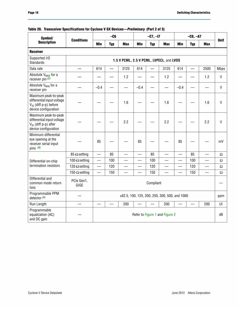
Table 20 lists the Cyclone V GX transceiver specifications.
Table 20. Transceiver Specifications for Cyclone V GX Devices—Preliminary (Part 1 of 3)
Symbol/Description Conditions
–C6 –C7, –I7 –C8, –A7
Min Typ Max Min Typ Max Min Typ Max
Reference Clock
Supported I/O Standards 1.2 V PCML, 1.5 V PCML, 2.5 V PCML, Differential LVPECL (1), HCSL, and LVDS
Input frequency from REFCLK input pins — 27 — 550 27 — 550 27 — 550
Duty cycle — 45 — 55 45 — 55 45 — 55
Peak-to-peak differential input voltage — 200 — 2000 200 — 2000 200 — 2000
Spread-spectrum modulating clock frequency
PCIe 30 — 33 30 — 33 30 — 33
Spread-spectrum downspread PCIe —
0 to
–0.5%— —
0 to
–0.5%— —
0 to
–0.5%—
On-chip termination resistors — — 100 — — 100 — — 100 —
VICM (AC coupled) — 1.1 1.1 1.1
VICM (DC coupled)
HCSL I/O standard for the PCIe reference
clock
250 — 550 250 — 550 250 — 550
RREF — — 2000 ±1% — — 2000
±1% — — 2000 ±1% —
Transceiver Clocks
fixedclk clock frequency
PCIeReceiver Detect — 125 — — 125 — — 125 —
Avalon® Memory- Mapped (Avalon-MM) PHY management clock frequency
< 150
June 2012 Altera Corporation Cyclone V Device Datasheet
Page 16 Switching Characteristics
Mbps
V
V
V
V
mV
Ω
Ω
Ω
Ω
—
ppm
UI
dB
Unit
Receiver
Supported I/O Standards 1.5 V PCML, 2.5 V PCML, LVPECL, and LVDS
Data rate — 614 — 3125 614 — 3125 614 — 2500
Absolute VMAX for a receiver pin (2) — — — 1.2 — — 1.2 — — 1.2
Absolute VMIN for a receiver pin — –0.4 — — –0.4 — — –0.4 — —
Maximum peak-to-peak differential input voltage VID (diff p-p) before device configuration
— — — 1.6 — — 1.6 — — 1.6
Maximum peak-to-peak differential input voltage VID (diff p-p) after device configuration
— — — 2.2 — — 2.2 — — 2.2
Minimum differential eye opening at the receiver serial input pins (3)
— 85 — — 85 — — 85 — —
Differential on-chip termination resistors
85−Ω setting — 85 — — 85 — — 85 —
100−Ω setting — 100 — — 100 — — 100 —
120−Ω setting — 120 — — 120 — — 120 —
150-Ω setting — 150 — — 150 — — 150 —
Differential and common mode return loss
PCIe Gen1, GIGE Compliant
Programmable PPM detector (4) — ±62.5, 100, 125, 200, 250, 300, 500, and 1000
Run Length — — — 200 — — 200 — — 200
Programmable equalization (AC)and DC gain
— Refer to Figure 1 and Figure 2
Table 20. Transceiver Specifications for Cyclone V GX Devices—Preliminary (Part 2 of 3)
Symbol/Description Conditions
–C6 –C7, –I7 –C8, –A7
Min Typ Max Min Typ Max Min Typ Max
Cyclone V Device Datasheet June 2012 Altera Corporation

Switching Characteristics Page 17
Mbps
mV
Ω
Ω
Ω
Ω
ps
ps
Mbps
MHz
MHz
the
Unit
Transmitter
Supported I/O Standards 1.5 V PCML
Data rate — 614 — 3125 614 — 3125 614 — 2500
VOCM — — 650 — — 650 — — 650 —
Differential on-chip termination resistors
85−Ω setting — 85 — — 85 — — 85 —
100−Ω setting — 100 — — 100 — — 100 —
120−Ω setting — 120 — — 120 — — 120 —
150-Ω setting — 150 — — 150 — — 150 —
Rise time (5) — 30 — 160 30 — 160 30 — 160
Fall time (5) — 30 — 160 30 — 160 30 — 160
CMU PLL
Supported data range — 614 — 3125 614 — 3125 614 — 2500
Transceiver-FPGA Fabric Interface
Interface speed (single-width mode) — 25 — 187.5 25 — 163.84 25 — 156.25
Interface speed (double-width mode) — 25 — 163.84 25 — 163.84 25 — 156.25
Notes to Table 20:
(1) Differential LVPECL signal levels must comply to the minimum and maximum peak-to-peak differential input voltage specified in this table.(2) The device cannot tolerate prolonged operation at this absolute maximum.(3) The differential eye opening specification at the receiver input pins assumes that you have disabled the Receiver Equalization feature. If you enable
Receiver Equalization feature, the receiver circuitry can tolerate a lower minimum eye opening, depending on the equalization level. (4) The rate matcher supports only up to ±300 parts per million (ppm).(5) The Quartus II software automatically selects the appropriate slew rate depending on the configured data rate or functional mode.
Table 20. Transceiver Specifications for Cyclone V GX Devices—Preliminary (Part 3 of 3)
Symbol/Description Conditions
–C6 –C7, –I7 –C8, –A7
Min Typ Max Min Typ Max Min Typ Max
June 2012 Altera Corporation Cyclone V Device Datasheet

Page 18 Switching Characteristics
Table 21 lists the Cyclone V GX transceiver block jitter specifications.
Table 21. Transceiver Block Jitter Specifications for Cyclone V GX Devices—Preliminary
Symbol/Description Conditions
–C6 –C7, –I7 –C8, –A7Unit
Min Typ Max Min Typ Max Min Typ Max
PCIe Transmit Jitter Generation (1)
Total jitter at 2.5 Gbps (Gen1) Compliance pattern — — 0.25 — — 0.25 — — 0.25 UI
PCIe Receiver Jitter Tolerance (1)
Total jitter at 2.5 Gbps (Gen1) Compliance pattern > 0.6 > 0.6 > 0.6 UI
GIGE Transmit Jitter Generation (2)
Deterministic jitter (peak-to-peak) Pattern = CRPAT — — 0.14 — — 0.14 — — 0.14 UI
Total jitter (peak-to-peak) Pattern = CRPAT — — 0.279 — — 0.279 — — 0.279 UI
GIGE Receiver Jitter Tolerance (2)
Deterministic jitter tolerance (peak-to-peak)
Pattern = CJPAT > 0.4 > 0.4 > 0.4 UI
Combined deterministic and random jitter tolerance (peak-to-peak)
Pattern = CJPAT > 0.66 > 0.66 > 0.66 UI
Notes to Table 21:
(1) The jitter numbers for PIPE are compliant to the PCIe Base Specification 2.0.(2) The jitter numbers for GIGE are compliant to the IEEE802.3-2002 Specification.
Cyclone V Device Datasheet June 2012 Altera Corporation

Switching Characteristics Page 19
Figure 1 shows the continuous time-linear equalizer (CTLE) response for Cyclone V devices with data rates > 3.25 Gbps.
Figure 1. CTLE Response for Cyclone V Devices with Data Rates > 3.25 Gbps
June 2012 Altera Corporation Cyclone V Device Datasheet

Page 20 Switching Characteristics
Figure 2 shows the CTLE response for Cyclone V devices with data rates ≤3.25 Gbps.
Figure 2. CTLE Response for Cyclone V Devices with Data Rates ≤3.25 Gbps
Cyclone V Device Datasheet June 2012 Altera Corporation

Switching Characteristics Page 21
Table 22 lists the TX VOD settings for Cyclone V transceiver channels.
Table 22. Typical TX VOD Setting for Cyclone V Transceiver Channels = 100 Ω—Preliminary
Symbol VOD Setting (1) VOD Value (mV) VOD Setting (1) VOD Value (mV)
VOD differential peak to peak typical
0 0 32 640
1 20 33 660
2 40 34 680
3 60 35 700
4 80 36 720
5 100 37 740
6 120 38 760
7 140 39 780
8 160 40 800
9 180 41 820
10 200 42 840
11 220 43 860
12 240 44 880
13 260 45 900
14 280 46 920
15 300 47 940
16 320 48 960
17 340 49 980
18 360 50 1000
19 380 51 1020
20 400 52 1040
21 420 53 1060
22 440 54 1080
23 460 55 1100
24 480 56 1120
25 500 57 1140
26 520 58 1160
27 540 59 1180
28 560 60 1200
29 580 61 1220
30 600 62 1240
31 620 63 1260
Note to Table 22:
(1) Convert these values to their binary equivalent form if you are using the dynamic reconfiguration mode for PMA analog controls.
June 2012 Altera Corporation Cyclone V Device Datasheet

Page 22 Switching Characteristics
Table 23 lists the simulation data on the transmitter pre-emphasis levels in dB for the first post tap under the following conditions:
■ Low-frequency data pattern—five 1s and five 0s
■ Data rate—2.5 Gbps
The levels listed are a representation of possible pre-emphasis levels under the specified conditions only and the pre-emphasis levels may change with data pattern and data rate.
1 To predict the pre-emphasis level for your specific data rate and pattern, run simulations using the Cyclone V HSSI HSPICE models.
Table 23. Transmitter Pre-Emphasis Levels for Cyclone V Devices (1), (2), (3), (4)—Preliminary (Part 1 of 2)
Quartus II 1st Post Tap Pre-Emphasis Setting
Quartus II VOD Setting
Unit10 (200 mV)
20 (400 mV)
30 (600 mV)
35 (700 mV)
40 (800 mV)
45 (900 mV)
50 (1000 mV)
0 0 0 0 0 0 0 0 dB
1 1.97 0.88 0.43 0.32 0.24 0.19 0.13 dB
2 3.58 1.67 0.95 0.76 0.61 0.5 0.41 dB
3 5.35 2.48 1.49 1.2 1 0.83 0.69 dB
4 7.27 3.31 2 1.63 1.36 1.14 0.96 dB
5 — 4.19 2.55 2.1 1.76 1.49 1.26 dB
6 — 5.08 3.11 2.56 2.17 1.83 1.56 dB
7 — 5.99 3.71 3.06 2.58 2.18 1.87 dB
8 — 6.92 4.22 3.47 2.93 2.48 2.11 dB
9 — 7.92 4.86 4 3.38 2.87 2.46 dB
10 — 9.04 5.46 4.51 3.79 3.23 2.77 dB
11 — 10.2 6.09 5.01 4.23 3.61 — dB
12 — 11.56 6.74 5.51 4.68 3.97 — dB
13 — 12.9 7.44 6.1 5.12 4.36 — dB
14 — 14.44 8.12 6.64 5.57 4.76 — dB
15 — — 8.87 7.21 6.06 5.14 — dB
16 — — 9.56 7.73 6.49 — — dB
17 — — 10.43 8.39 7.02 — — dB
18 — — 11.23 9.03 7.52 — — dB
19 — — 12.18 9.7 8.02 — — dB
20 — — 13.17 10.34 8.59 — — dB
21 — — 14.2 11.1 — — — dB
22 — — 15.38 11.87 — — — dB
23 — — — 12.67 — — — dB
24 — — — 13.48 — — — dB
Cyclone V Device Datasheet June 2012 Altera Corporation

Switching Characteristics Page 23
25 — — — 14.37 — — — dB
26 — — — — — — — dB
27 — — — — — — — dB
28 — — — — — — — dB
29 — — — — — — — dB
30 — — — — — — — dB
31 — — — — — — — dB
Notes to Table 23:
(1) The 1st post tap pre-emphasis settings must satisfy |B| + |C| ≤ 60|B| = VOD setting with termination value, RTERM = 100 Ω|C| = 1st post tap pre-emphasis setting
(2) |B| – |C| > 5 for data rates < 5 Gbps and |B| – |C| > 8.25 for data rates > 5 Gbps.(3) (VMAX/VMIN – 1)% < 600%, where VMAX = |B| + |C| and VMIN = |B| – |C|.(4) For example, when VOD = 800 mV, the corresponding VOD value setting is 40.
To check the validity of the 1st post tap pre-emphasis setting = 2|B| + |C| ≤ 60 → 40 + 2 = 42|B| –|C| > 5 → 40 – 2 = 38(VMAX/VMIN – 1)% < 600% → (42/38 – 1)% = 10.52%Therefore, the 1st post tap pre-emphasis setting = 2 is a valid condition.
Table 23. Transmitter Pre-Emphasis Levels for Cyclone V Devices (1), (2), (3), (4)—Preliminary (Part 2 of 2)
Quartus II 1st Post Tap Pre-Emphasis Setting
Quartus II VOD Setting
Unit10 (200 mV)
20 (400 mV)
30 (600 mV)
35 (700 mV)
40 (800 mV)
45 (900 mV)
50 (1000 mV)
June 2012 Altera Corporation Cyclone V Device Datasheet

Page 24 Switching Characteristics
Core Performance SpecificationsThis section describes the clock tree, phase-locked loop (PLL), digital signal processing (DSP), and memory block specifications.
Clock Tree SpecificationsTable 24 lists the clock tree specifications for Cyclone V devices.
PLL SpecificationsTable 25 lists the Cyclone V PLL specifications when operating in the commercial (0° to 85°C), industrial (–40° to 100°C), and automotive (–40° to 125°C) junction temperature ranges.
Table 24. Clock Tree Performance for Cyclone V Devices—Preliminary
PerformanceUnit
Symbol –C6 –C7, –I7 –C8, –A7
Global clock and Regional clock 550 550 460 MHz
Peripheral clock 155 155 155 MHz
Table 25. PLL Specifications for Cyclone V Devices (1)—Preliminary (Part 1 of 3)
Symbol Parameter Min Typ Max Unit
fIN Input clock frequency
–C6 speed grade 5 — 670 (2) MHz
–C7, –I7 speed grades 5 — 622 (2) MHz
–C8, –A7 speed grades 5 — 500 (2) MHz
fINPFD Integer input clock frequency to the PFD 5 — 325 MHz
fFINPFD Fractional input clock frequency to the PFD 50 — TBD (1) MHz
fVCO(3) PLL VCO operating range
–C6 speed grade 600 — 1600 MHz
–C7, –I7 speed grades 600 — 1400 MHz
–C8, –A7 speed grades 600 — 1300 MHz
tEINDUTY Input clock or external feedback clock input duty cycle 40 — 60 %
fOUTOutput frequency for internal global or regional clock
–C6 speed grade — — 550 (4) MHz
–C7, –I7 speed grades — — 550 (4) MHz
–C8, –A7 speed grades — — 460 (4) MHz
fOUT_EXTOutput frequency for external clock output
–C6 speed grade — — 667 (4) MHz
–C7, –I7 speed grades — — 667 (4) MHz
–C8, –A7 speed grades — — 533 (4) MHz
tOUTDUTY Duty cycle for external clock output (when set to 50%) 45 50 55 %
tFCOMP External feedback clock compensation time — — 10 ns
tCONFIGPHASE Time required to reconfigure phase shift — — TBD (1) —
tDYCONFIGCLK Dynamic configuration clock — — 100 MHz
tLOCKTime required to lock from end-of-device configuration or deassertion of areset — — 1 ms
tDLOCKTime required to lock dynamically (after switchover or reconfiguring any non-post-scale counters/delays) — — 1 ms
Cyclone V Device Datasheet June 2012 Altera Corporation

Switching Characteristics Page 25
fCLBW
PLL closed-loop low bandwidth — 0.3 — MHz
PLL closed-loop medium bandwidth — 1.5 — MHz
PLL closed-loop high bandwidth (9) — 4 — MHz
tPLL_PSERR Accuracy of PLL phase shift — — ±50 ps
tARESET Minimum pulse width on the areset signal 10 — — ns
tINCCJ (5), (6)Input clock cycle-to-cycle jitter (FREF ≥ 100 MHz) — — 0.15 UI (p-p)
Input clock cycle-to-cycle jitter (FREF < 100 MHz) — — ±750 ps (p-p)
tOUTPJ_DC (7)Period jitter for dedicated clock output (FOUT ≥ 100 MHz) — — TBD (1) ps (p-p)
Period jitter for dedicated clock output (FOUT < 100 MHz) — — TBD (1) mUI (p-p)
tOUTCCJ_DC (7)
Cycle-to-cycle jitter for dedicated clock output (FOUT ≥ 100 MHz) — — TBD (1) ps (p-p)
Cycle-to-cycle jitter for dedicated clock output(FOUT < 100 MHz) — — TBD (1) mUI (p-p)
tOUTPJ_IO (7), (10)
Period jitter for clock output on regular I/O (FOUT ≥ 100 MHz) — — TBD (1) ps (p-p)
Period jitter for clock output on regular I/O (FOUT < 100 MHz) — — TBD (1) mUI (p-p)
tOUTCCJ_IO (7), (10)
Cycle-to-cycle jitter for clock output on regular I/O (FOUT ≥ 100 MHz) — — TBD (1) ps (p-p)
Cycle-to-cycle jitter for clock output on regular I/O (FOUT < 100 MHz) — — TBD (1) mUI (p-p)
tOUTPJ_DC_F Period jitter for dedicated clock output in fractional mode — — TBD (1) —
tOUTCCJ_DC_FCycle-to-cycle jitter for dedicated clock output in fractional mode — — TBD (1) —
tOUTPJ_IO_F Period jitter for clock output on regular I/O in fractional mode — — TBD (1) —
tOUTCCJ_IO_FCycle-to-cycle jitter for clock output on regular I/O in fractional mode — — TBD (1) —
tCASC_OUTPJ_DC (7), (8)
Period jitter for dedicated clock output in cascaded PLLs (FOUT ≥ 100 MHz) — — TBD (1) ps (p-p)
Period jitter for dedicated clock output in cascaded PLLs (FOUT < 100 MHz) — — TBD (1) mUI (p-p)
Table 25. PLL Specifications for Cyclone V Devices (1)—Preliminary (Part 2 of 3)
Symbol Parameter Min Typ Max Unit
June 2012 Altera Corporation Cyclone V Device Datasheet

Page 26 Switching Characteristics
DSP Block Specifications Table 26 lists the Cyclone V DSP block performance specifications.
tDRIFTFrequency drift after PFDENA is disabled for a duration of 100 µs — — ±10 %
dKBIT Bit number of Delta Sigma Modulator (DSM) — 24 — Bits
kVALUE Numerator of Fraction TBD (1) 8388608 TBD (1) —
fRES Resolution of VCO frequency (fINPFD =100 MHz) — 5.96 — Hz
Notes to Table 25:
(1) Pending silicon characterization. (2) This specification is limited in the Quartus II software by the I/O maximum frequency. The maximum I/O frequency is different for each I/O standard. (3) The VCO frequency reported by the Quartus II software takes into consideration the VCO post-scale counter K value. Therefore, if the counter K has
a value of 2, the frequency reported can be lower than the fVCO specification.(4) This specification is limited by the lower of the two: I/O fMAX or FOUT of the PLL.(5) A high input jitter directly affects the PLL output jitter. To have low PLL output clock jitter, you must provide a clean clock source < 120 ps.(6) FREF is fIN/N when N = 1.(7) Peak-to-peak jitter with a probability level of 10–12 (14 sigma, 99.99999999974404% confidence level). The output jitter specification applies to
the intrinsic jitter of the PLL, when an input jitter of 30 ps is applied. The external memory interface clock output jitter specifications use a different measurement method and are available in Table 31 on page 1–30.
(8) The cascaded PLL specification is only applicable with the following condition:a. Upstream PLL: 0.59 MHz ≤ Upstream PLL BW < 1 MHz b. Downstream PLL: Downstream PLL BW > 2 MHz
(9) High bandwidth PLL settings are not supported in external feedback mode.(10) External memory interface clock output jitter specifications use a different measurement method, which is available in Table 31 on page 1–30.
Table 25. PLL Specifications for Cyclone V Devices (1)—Preliminary (Part 3 of 3)
Symbol Parameter Min Typ Max Unit
Table 26. DSP Block Performance Specifications for Cyclone V Devices—Preliminary
ModePerformance
Unit–C6 –C7, –I7 –C8, –A7
Modes using One DSP Block
Independent 9 x 9 Multiplication 340 300 260 MHz
Independent 18 x 19 Multiplication 287 250 200 MHz
Independent 18 x 18 Multiplication 287 250 200 MHz
Independent 27 x 27 Multiplication 250 200 160 MHz
Independent 18 x 25 Multiplication 310 250 200 MHz
Independent 20 x 24 Multiplication 310 250 200 MHz
Two 18 x 19 Multiplier Adder Mode 310 250 200 MHz
18 x 18 Multiplier Added Summed with 36-bit Input 310 250 200 MHz
Modes using Two DSP Blocks
Complex 18 x 19 multiplication 310 250 200 MHz
Cyclone V Device Datasheet June 2012 Altera Corporation

Switching Characteristics Page 27
Memory Block SpecificationsTable 27 lists the Cyclone V memory block specifications.
Periphery PerformanceThis section describes periphery performance and the high-speed I/O and external memory interface.
1 Actual achievable frequency depends on design- and system-specific factors. You must perform HSPICE/IBIS simulations based on your specific design and system setup to determine the maximum achievable frequency in your system.
Table 27. Memory Block Performance Specifications for Cyclone V Devices (1), (2) —Preliminary
Memory ModeResources Used Performance
UnitALUTs Memory –C6 –C7, –I7 –C8, –A7
MLAB
Single port, all supported widths 0 1 450 380 330 MHz
Simple dual-port, all supported widths 0 1 450 380 330 MHz
Simple dual-port with read and write at the same address 0 1 350 300 250 MHz
ROM, all supported width 0 1 450 380 330 MHz
M10K Block
Single-port, all supported widths 0 1 315 275 240 MHz
Simple dual-port, all supported widths 0 1 315 275 240 MHz
Simple dual-port with the read-during-write option set to Old Data, all supported widths
0 1 275 240 180 MHz
True dual port, all supported widths 0 1 315 275 240 MHz
ROM, all supported widths 0 1 315 275 240 MHz
Min Pulse Width (clock high time) — — 1,450 1,550 1,650 ps
Min Pulse Width (clock low time) — — 1,000 1,200 1,350 ps
Notes to Table 27:
(1) To achieve the maximum memory block performance, use a memory block clock that comes through global clock routing from an on-chip PLL set to 50% output duty cycle. Use the Quartus II software to report timing for this and other memory block clocking schemes.
(2) When you use the error detection cyclical redundancy check (CRC) feature, there is no degradation in fMAX.
June 2012 Altera Corporation Cyclone V Device Datasheet
Page 28 Switching Characteristics
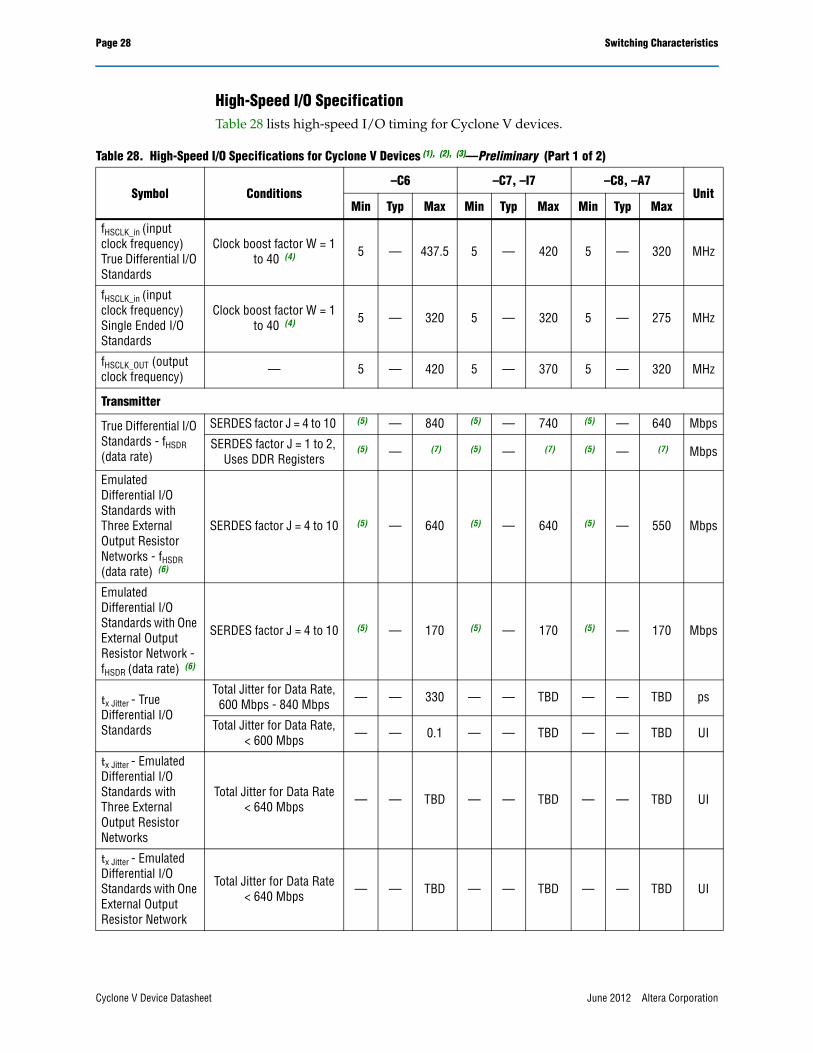
High-Speed I/O SpecificationTable 28 lists high-speed I/O timing for Cyclone V devices.
Table 28. High-Speed I/O Specifications for Cyclone V Devices (1), (2), (3)—Preliminary (Part 1 of 2)
Symbol Conditions–C6 –C7, –I7 –C8, –A7
UnitMin Typ Max Min Typ Max Min Typ Max
fHSCLK_in (input clock frequency) True Differential I/O Standards
Clock boost factor W = 1 to 40 (4) 5 — 437.5 5 — 420 5 — 320 MHz
fHSCLK_in (input clock frequency) Single Ended I/O Standards
Clock boost factor W = 1 to 40 (4) 5 — 320 5 — 320 5 — 275 MHz
fHSCLK_OUT (output clock frequency) — 5 — 420 5 — 370 5 — 320 MHz
Transmitter
True Differential I/O Standards - fHSDR (data rate)
SERDES factor J = 4 to 10 (5) — 840 (5) — 740 (5) — 640 Mbps
SERDES factor J = 1 to 2, Uses DDR Registers
(5) — (7) (5) — (7) (5) — (7) Mbps
Emulated Differential I/O Standards with Three External Output Resistor Networks - fHSDR (data rate) (6)
SERDES factor J = 4 to 10 (5) — 640 (5) — 640 (5) — 550 Mbps
Emulated Differential I/O Standards with One External Output Resistor Network - fHSDR (data rate) (6)
SERDES factor J = 4 to 10 (5) — 170 (5) — 170 (5) — 170 Mbps
tx Jitter - True Differential I/O Standards
Total Jitter for Data Rate, 600 Mbps - 840 Mbps — — 330 — — TBD — — TBD ps
Total Jitter for Data Rate, < 600 Mbps — — 0.1 — — TBD — — TBD UI
tx Jitter - Emulated Differential I/O Standards with Three External Output Resistor Networks
Total Jitter for Data Rate < 640 Mbps — — TBD — — TBD — — TBD UI
tx Jitter - Emulated Differential I/O Standards with One External Output Resistor Network
Total Jitter for Data Rate < 640 Mbps — — TBD — — TBD — — TBD UI
Cyclone V Device Datasheet June 2012 Altera Corporation

Switching Characteristics Page 29
tDUTY
TX output clock duty cycle for both True and
Emulated Differential I/O Standards
45 50 55 45 50 55 45 50 55 %
tRISE & tFALL
True Differential I/O Standards — — 200 — — 200 — — 200 ps
Emulated Differential I/O Standards with Three
External Output Resistor Networks
— — 250 — — 250 — — 300 ps
Emulated Differential I/O Standards with One
External Output Resistor Network
— — 300 — — 300 — — 300 ps
TCCS
True Differential I/O Standards — — 200 — — 250 — — 250 ps
Emulated Differential I/O Standards with Three
External Output Resistor Networks
— — 300 — — 300 — — 300 ps
Emulated Differential I/O Standards with One
External Output Resistor Network
— — 300 — — 300 — — 300 ps
Receiver
fHSDR (data rate)SERDES factor J = 4 to 10 (5) — 875 (6) (5) — 840 (6) (5) — 640 (6) Mbps
SERDES factor J = 1 to 2, Uses DDR Registers
(5) — (7) (5) — (7) (5) — (7) Mbps
Sampling Window — — — 350 — — 350 — — 350 ps
Notes to Table 28:
(1) When J = 1 or 2, bypass the serializer/deserializer (SERDES) block.(2) For LVDS applications, you must use the PLLs in integer PLL mode.(3) This is achieved by using the LVDS clock network.(4) Clock Boost Factor (W) is the ratio between the input data rate and the input clock rate.(5) The minimum specification depends on the clock source (for example, the PLL and clock pin) and the clock routing resource (global, regional,
or local) that you use. The I/O differential buffer and input register do not have a minimum toggle rate.(6) You must calculate the leftover timing margin in the receiver by performing link timing closure analysis. You must consider the board skew
margin, transmitter channel-to-channel skew, and receiver sampling margin to determine the leftover timing margin.(7) The maximum ideal frequency is the SERDES factor (J) x PLL max output frequency (fout), provided you can close the design timing and the
signal integrity simulation is clean.You can estimate the achievable maximum data rate by performing link timing closure analysis. You must consider the board skew margin, transmitter delay margin, and receiver sampling margin to determine the maximum data rate supported.
Table 28. High-Speed I/O Specifications for Cyclone V Devices (1), (2), (3)—Preliminary (Part 2 of 2)
Symbol Conditions–C6 –C7, –I7 –C8, –A7
UnitMin Typ Max Min Typ Max Min Typ Max
June 2012 Altera Corporation Cyclone V Device Datasheet

Page 30 Switching Characteristics
DLL Range, DQS Logic Block and Memory Output Clock Jitter Specifications Table 29 lists the DLL operating frequency range specifications for Cyclone V devices.
Table 30 lists the DQS phase shift error for Cyclone V devices.
Table 31 lists the memory output clock jitter specifications for Cyclone V devices.
Table 29. DLL Operating Frequency Range Specifications for Cyclone V Devices
Parameter –C6 –C7, –I7 –C8 Unit
DLL operating frequency range 167 – 400 167 – 400 167 – 400 MHz
Table 30. DQS Phase Shift Error Specification for DLL-Delayed Clock (tDQS_PSERR) for Cyclone V Devices (1), (2) —Preliminary
Number of DQS Delay Buffers –C6 –C7, –I7 –C8 Unit
2 40 80 80 ps
Notes to Table 30:
(1) The numbers are preliminary pending silicon characterization. (2) This error specification is the absolute maximum and minimum error.
Table 31. Memory Output Clock Jitter Specification for Cyclone V Devices (1), (2), (3) —Preliminary
Parameter Clock Network Symbol
–C6 –C7, –I7 –C8Unit
Min Max Min Max Min Max
Clock period jitter PHYCLK tJIT(per) –90 90 –90 90 –90 90 ps
Cycle-to-cycle period jitter PHYCLK tJIT(cc) 180 180 180 ps
Notes to Table 31:
(1) The memory output clock jitter measurements are for 200 consecutive clock cycles, as specified in the JEDEC DDR2/DDR3 SDRAM standard.(2) Altera recommends using the UniPHY intellectual property (IP) with PHYCLK connections that has better jitter performance.(3) The memory output clock jitter is applicable when an input jitter of 30 ps (p-p) is applied with bit error rate (BER) -12, equivalent to 14 sigma.
Cyclone V Device Datasheet June 2012 Altera Corporation

Switching Characteristics Page 31
OCT Calibration Block SpecificationsTable 32 lists the OCT calibration block specifications for Cyclone V devices.
Figure 3 shows the timing diagram for the oe and dyn_term_ctrl signals.
Duty Cycle Distortion (DCD) SpecificationsTable 33 lists the worst-case DCD for Cyclone V devices.
Table 32. OCT Calibration Block Specifications for Cyclone V Devices—Preliminary
Symbol Description Min Typ Max Unit
OCTUSRCLK Clock required by OCT calibration blocks — — 20 MHz
TOCTCALNumber of OCTUSRCLK clock cycles required forRS OCT /RT OCT calibration — 1000 — Cycles
TOCTSHIFTNumber of OCTUSRCLK clock cycles required for OCT code to shift out — 32 — Cycles
TRS_RT
Time required between the dyn_term_ctrl and oe signal transitions in a bidirectional I/O buffer to dynamically switch between RS OCT and RT OCT
— 2.5 — ns
Figure 3. Timing Diagram for the oe and dyn_term_ctrl Signals
[
Table 33. Worst-Case DCD on I/O Pins for Cyclone V Devices—Preliminary
Symbol–C6 –C7, –I7 –C8, –A7
UnitMin Max Min Max Min Max
Output Duty Cycle 45 55 45 55 45 55 %
TX RXRX
oe
dyn_term_ctrl
TRS_RTTRS_RT
Tristate Tristate
June 2012 Altera Corporation Cyclone V Device Datasheet
Page 32 Configuration Specification
Configuration SpecificationThis section provides configuration specifications and timing for Cyclone V devices.
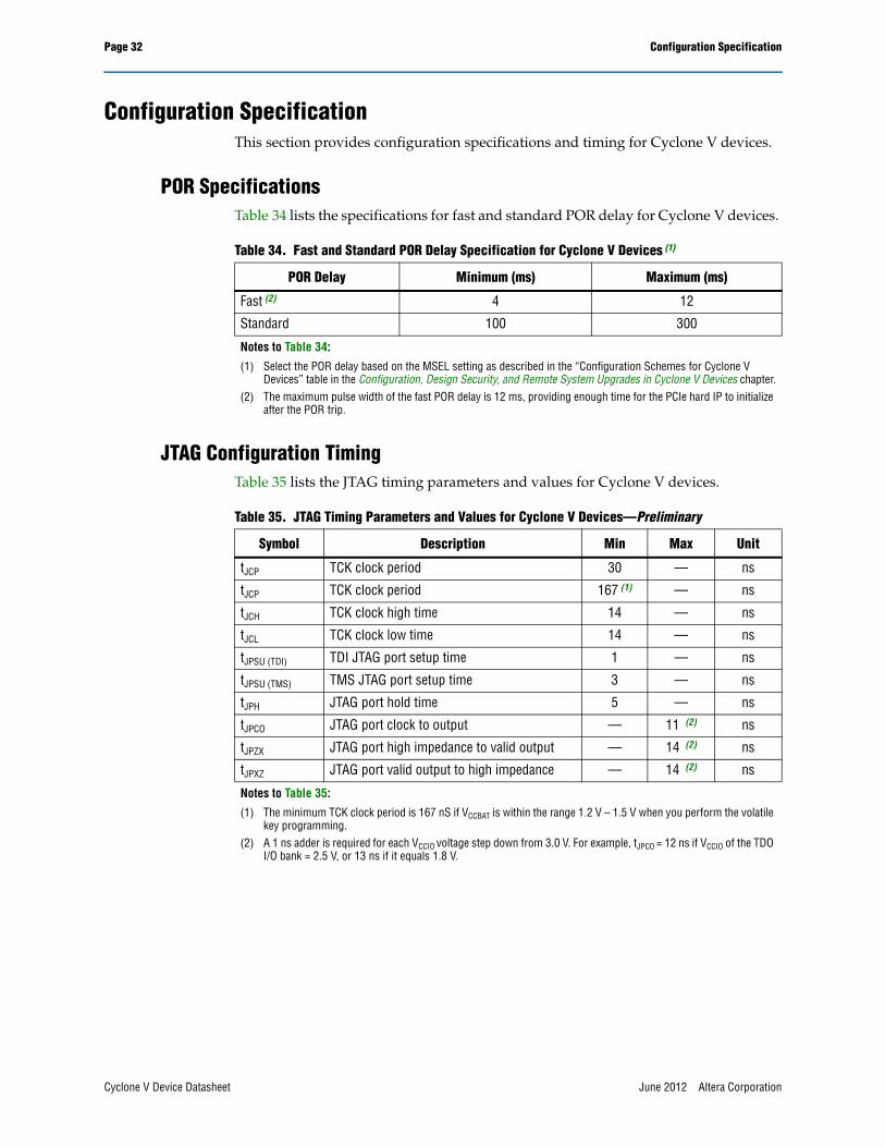
POR SpecificationsTable 34 lists the specifications for fast and standard POR delay for Cyclone V devices.
JTAG Configuration TimingTable 35 lists the JTAG timing parameters and values for Cyclone V devices.
Table 34. Fast and Standard POR Delay Specification for Cyclone V Devices (1)
POR Delay Minimum (ms) Maximum (ms)
Fast (2) 4 12
Standard 100 300
Notes to Table 34:
(1) Select the POR delay based on the MSEL setting as described in the “Configuration Schemes for Cyclone V Devices” table in the Configuration, Design Security, and Remote System Upgrades in Cyclone V Devices chapter.
(2) The maximum pulse width of the fast POR delay is 12 ms, providing enough time for the PCIe hard IP to initialize after the POR trip.
Table 35. JTAG Timing Parameters and Values for Cyclone V Devices—Preliminary
Symbol Description Min Max Unit
tJCP TCK clock period 30 — ns
tJCP TCK clock period 167 (1) — ns
tJCH TCK clock high time 14 — ns
tJCL TCK clock low time 14 — ns
tJPSU (TDI) TDI JTAG port setup time 1 — ns
tJPSU (TMS) TMS JTAG port setup time 3 — ns
tJPH JTAG port hold time 5 — ns
tJPCO JTAG port clock to output — 11 (2) ns
tJPZX JTAG port high impedance to valid output — 14 (2) ns
tJPXZ JTAG port valid output to high impedance — 14 (2) ns
Notes to Table 35:
(1) The minimum TCK clock period is 167 nS if VCCBAT is within the range 1.2 V – 1.5 V when you perform the volatile key programming.
(2) A 1 ns adder is required for each VCCIO voltage step down from 3.0 V. For example, tJPCO = 12 ns if VCCIO of the TDO I/O bank = 2.5 V, or 13 ns if it equals 1.8 V.
Cyclone V Device Datasheet June 2012 Altera Corporation

Configuration Specification Page 33
FPP Configuration TimingThis section describes the fast passive parallel (FPP) configuration timing parameters for Cyclone V devices.
DCLK-to-DATA[] Ratio (r) for FPP ConfigurationFPP configuration requires a different DCLK-to-DATA[] ratio when you turn on encryption or the compression feature.
Table 36 lists the DCLK-to-DATA[] ratio for each combination.
1 If the DCLK-to-DATA[] ratio is greater than 1, at the end of configuration, you can only stop the DCLK (DCLK-to-DATA[] ratio – 1) clock cycles after the last data is latched into the Cyclone V device.
Table 36. DCLK-to-DATA[] Ratio for Cyclone V Devices (1)—Preliminary
Configuration Scheme Encryption Compression DCLK-to-DATA[] ratio (r)
FPP (8-bit wide)
Off Off 1
On Off 1
Off On 2
On On 2
FPP (16-bit wide)
Off Off 1
On Off 2
Off On 4
On On 4
Note to Table 36:
(1) Depending on the DCLK-to-DATA[] ratio, the host must send a DCLK frequency that is r times the DATA[] rate in byte per second (Bps) or word per second (Wps). For example, in FPP x16 where the r is 2, the DCLK frequency must be 2 times the DATA[] rate in Wps. Cyclone V devices use additional clock cycles to decrypt and decompress the configuration data.
June 2012 Altera Corporation Cyclone V Device Datasheet

Page 34 Configuration Specification
FPP Configuration Timing when DCLK to DATA[] = 1Figure 4 shows the timing waveform for an FPP configuration when using a MAX® II device as an external host. This waveform shows timing when the DCLK-to-DATA[] ratio is 1.
1 When you enable decompression or the design security feature, the DCLK-to-DATA[] ratio varies for FPP x8 and FPP x16. For the respective DCLK-to-DATA[] ratio, refer to Table 36 on page 1–33.
Figure 4. DCLK-to-DATA[] FPP Configuration Timing Waveform for Cyclone V Devices When the Ratio is 1 (1)
Notes to Figure 4:
(1) The beginning of this waveform shows the device in user mode. In user mode, nCONFIG, nSTATUS, and CONF_DONE are at logic-high levels. When nCONFIG is pulled low, a reconfiguration cycle begins.
(2) After power up, the Cyclone V device holds nSTATUS low for the time of the POR delay.(3) After power up, before and during configuration, CONF_DONE is low.(4) Do not leave DCLK floating after configuration. You can drive it high or low, whichever is more convenient.(5) For FPP x16, use DATA[15..0]. For FPP x8, use DATA[7..0]. DATA[15..0] are available as a user I/O pin after configuration. The state of this
pin depends on the dual-purpose pin settings.(6) To ensure a successful configuration, send the entire configuration data to the Cyclone V device. CONF_DONE is released high when the Cyclone V
device receives all the configuration data successfully. After CONF_DONE goes high, send two additional falling edges on DCLK to begin initialization and enter user mode.
(7) After the option bit to enable the INIT_DONE pin is configured into the device, INIT_DONE goes low.
nCONFIG
nSTATUS (2)
CONF_DONE (3)
DCLK
DATA[15..0]
User I/O
INIT_DONE
Word 0 Word 1 Word 2 Word 3
tCD2UM
tCF2ST1
tCF2CD
tCFG
tCH tCL
tDH
tDSU
tCF2CK
tSTATUS
tCLKtCF2ST0
tST2CK
High-Z User Mode
(5)
(7)
(4)
User ModeWord n-2 Word n-1 Word n
(6)
Cyclone V Device Datasheet June 2012 Altera Corporation

Configuration Specification Page 35
Table 37 lists the timing parameters for Cyclone V devices for an FPP configuration when the DCLK-to-DATA[] ratio is 1.
Table 37. DCLK-to-DATA[] FPP Timing Parameters for Cyclone V Devices When the Ratio is 1 (1)—Preliminary
Symbol Parameter Minimum Maximum Unit
tCF2CD nCONFIG low to CONF_DONE low — 600 ns
tCF2ST0 nCONFIG low to nSTATUS low — 600 ns
tCFG nCONFIG low pulse width 2 — µs
tSTATUS nSTATUS low pulse width 268 1506 (2) µs
tCF2ST1 nCONFIG high to nSTATUS high — 1506 (3) µs
tCF2CK nCONFIG high to first rising edge on DCLK 1506 — µs
tST2CK nSTATUS high to first rising edge of DCLK 2 — µs
tDSUDATA[] setup time before rising edge on DCLK
5.5 — ns
tDH DATA[] hold time after rising edge on DCLK 0 — ns
tCH DCLK high time 0.45 x 1/fMAX — s
tCL DCLK low time 0.45 x 1/fMAX — s
tCLK DCLK period 1/fMAX — s
fMAX DCLK frequency (FPP x8 and x16) — 125 MHz
tCD2UM CONF_DONE high to user mode (4) 175 437 µs
tCD2CU CONF_DONE high to CLKUSR enabled 4 × maximum DCLK period — —
tCD2UMC CONF_DONE high to user mode with CLKUSR option on
tCD2CU + (Tinit x CLKUSR
period)— —
TinitNumber of clock cycles required for device initialization 17,408 — Cycles
Notes to Table 37:
(1) Use these timing parameters when the DCLK-to-DATA[] ratio is 1. To find the DCLK-to-DATA[] ratio for your system, refer to Table 36 on page 1–33.
(2) You can obtain this value if you do not delay configuration by extending the nCONFIG or nSTATUS low pulse width.(3) You can obtain this value if you do not delay configuration by externally holding nSTATUS low.(4) The minimum and maximum numbers apply only if you chose the internal oscillator as the clock source for initializing the device.
June 2012 Altera Corporation Cyclone V Device Datasheet

Page 36 Configuration Specification
FPP Configuration Timing when DCLK to DATA[] > 1Figure 5 shows the timing waveform for an FPP configuration when using a MAX II device or microprocessor as an external host. This waveform shows timing when the DCLK-to-DATA[]ratio is more than 1.
Figure 5. FPP Configuration Timing Waveform for Cyclone V Devices When the DCLK-to-DATA[] Ratio is > 1 (1), (2)
Notes to Figure 5:
(1) To find the DCLK-to-DATA[] ratio for your system, refer to Table 36 on page 1–33.(2) The beginning of this waveform shows the device in user mode. In user mode, nCONFIG, nSTATUS, and CONF_DONE are at logic high levels.
When nCONFIG is pulled low, a reconfiguration cycle begins.(3) After power up, the Cyclone V device holds nSTATUS low for the time as specified by the POR delay.(4) After power up, before and during configuration, CONF_DONE is low.(5) Do not leave DCLK floating after configuration. You can drive it high or low, whichever is more convenient.(6) “r” denotes the DCLK-to-DATA[] ratio. For the DCLK-to-DATA[] ratio based on the decompression and the design security feature enable
settings, refer to Table 36 on page 1–33.(7) If needed, pause DCLK by holding it low. When DCLK restarts, the external host must provide data on the DATA[15..0] pins prior to sending
the first DCLK rising edge.(8) To ensure a successful configuration, send the entire configuration data to the Cyclone V device. CONF_DONE is released high after the Cyclone V
device receives all the configuration data successfully. After CONF_DONE goes high, send two additional falling edges on DCLK to begin initialization and enter user mode.
(9) After the option bit to enable the INIT_DONE pin is configured into the device, INIT_DONE goes low.
nCONFIG
nSTATUS (3)
CONF_DONE (4)
DCLK (6)
DATA[15..0] (8)
User I/O
INIT_DONE
tCD2UM
tCF2ST1
tCF2CD
tCFG
tCF2CK
ttCF2ST0
tST2CK
High-Z User Mode
1 2 r 1 2 r 1 2
Word 0 Word 1 Word 3
1
tDSUtDH
STATUS
tDH
tCH
tCL
tCLK
Word (n-1)
(7)
(8)
(9)
(5)
User Mode
r
Word n
Cyclone V Device Datasheet June 2012 Altera Corporation

Configuration Specification Page 37
Table 38 lists the timing parameters for Cyclone V devices when the DCLK-to-DATA[]ratio is more than 1.
Table 38. DCLK-to-DATA[] FPP Timing Parameters for Cyclone V Devices when the Ratio is > 1 (1)—Preliminary
Symbol Parameter Minimum Maximum Unit
tCF2CD nCONFIG low to CONF_DONE low — 600 ns
tCF2ST0 nCONFIG low to nSTATUS low — 600 ns
tCFG nCONFIG low pulse width 2 — µs
tSTATUS nSTATUS low pulse width 268 1506 (2) µs
tCF2ST1 nCONFIG high to nSTATUS high — 1506 (3) µs
tCF2CK nCONFIG high to first rising edge on DCLK 1506 — µs
tST2CK nSTATUS high to first rising edge of DCLK 2 — µs
tDSUDATA[] setup time before rising edge on DCLK
5.5 — ns
tDH DATA[] hold time after rising edge on DCLK N – 1/fDCLK(4) — s
tCH DCLK high time 0.45 x 1/fMAX — s
tCL DCLK low time 0.45 x 1/fMAX — s
tCLK DCLK period 1/fMAX — s
fMAX DCLK frequency (FPP x8 and x16) — 125 MHz
tR Input rise time — 40 ns
tF Input fall time — 40 ns
tCD2UM CONF_DONE high to user mode (5) 175 437 µs
tCD2CU CONF_DONE high to CLKUSR enabled 4 × maximum DCLK period — —
tCD2UMC CONF_DONE high to user mode with CLKUSR option on
tCD2CU + (Tinit x CLKUSR
period)— —
TinitNumber of clock cycles required for device initialization 17,408 — Cycles
Notes to Table 38:
(1) Use these timing parameters when you use decompression and the design security features.(2) This value can be obtained if you do not delay configuration by extending the nCONFIG or nSTATUS low pulse width.(3) This value can be obtained if you do not delay configuration by externally holding nSTATUS low.(4) N is the DCLK-to-DATA[] ratio and fDCLK is the DCLK frequency of the system. (5) The minimum and maximum numbers apply only if you chose the internal oscillator as the clock source for initializing the device.
June 2012 Altera Corporation Cyclone V Device Datasheet

Page 38 Configuration Specification
AS Configuration TimingFigure 6 shows the timing waveform for the active serial (AS) x1 mode and AS x4 mode configuration timing.
Table 39 lists the timing parameters for AS x1 and AS x4 configurations in Cyclone V devices.
Figure 6. AS Configuration Timing for Cyclone V Devices
Notes to Figure 6:
(1) The AS scheme supports standard and fast POR delay (tPOR). For tPOR delay information, refer to “POR Delay Specification” in the Configuration, Design Security, and Remote System Upgrades in Cyclone V Devices chapter.
(2) If you are using AS x4 mode, this signal represents the AS_DATA[3..0] and EPCQ sends in 4-bits of data for each DCLK cycle.(3) The initialization clock can be from the internal oscillator or the CLKUSR pin.(4) After the option bit to enable the INIT_DONE pin is configured into the device, INIT_DONE goes low.
Read Address
bit N - 1bit N bit 1 bit 0
tCD2UM
nSTATUS
nCONFIG
CONF_DONE
nCSO
DCLK
AS_DATA0/ASDO
AS_DATA1 (2)
INIT_DONE (4)
User I/O User Mode
tPOR
tDH
tSU
tCO
(1)
(3)
Table 39. AS Timing Parameters for AS x1 and x4 Configurations in Cyclone V Devices (1), (2)—Preliminary
Symbol Parameter Minimum Maximum Unit
tCO DCLK falling edge to the AS_DATA0/ASDO output — 4 µs
tSU Data setup time before the falling edge on DCLK 1.5 — ns
tH Data hold time after the falling edge on DCLK 0 — ns
tCD2UM CONF_DONE high to user mode 175 437 µs
tCD2CU CONF_DONE high to CLKUSR enabled 4 x maximum DCLK period — —
tCD2UMC CONF_DONE high to user mode with CLKUSR option on
tCD2CU + (Tinit x CLKUSR
period)— —
TinitNumber of clock cycles required for device initialization 17,408 — Cycles
Notes to Table 39:
(1) The minimum and maximum numbers apply only if you choose the internal oscillator as the clock source for initializing the device.(2) The tCF2CD, tCF2ST0, tCFG, tSTATUS, and tCF2ST1 timing parameters are identical to the timing parameters for passive serial (PS) mode listed in
Table 41 on page 1–40.
Cyclone V Device Datasheet June 2012 Altera Corporation

Configuration Specification Page 39
Table 40 lists the internal clock frequency specification for the AS configuration scheme.
PS Configuration TimingFigure 7 shows the timing waveform for a PS configuration when using a MAX II device or microprocessor as an external host.
Table 40. DCLK Frequency Specification in the AS Configuration Scheme for Cyclone V Devices (1), (2)—Preliminary
Minimum Typical Maximum Unit
5.3 7.9 12.5 MHz
10.6 15.7 25.0 MHz
21.3 31.4 50.0 MHz
42.6 62.9 100.0 MHz
Notes to Table 40:
(1) This applies to the DCLK frequency specification when using the internal oscillator as the configuration clock source.
(2) The AS multi-device configuration scheme does not support DCLK frequency of 100 MHz.
Figure 7. PS Configuration Timing Waveform for Cyclone V Devices (1)
Notes to Figure 7:
(1) The beginning of this waveform shows the device in user mode. In user mode, nCONFIG, nSTATUS, and CONF_DONE are at logic high levels. When nCONFIG is pulled low, a reconfiguration cycle begins.
(2) After power up, the Cyclone V device holds nSTATUS low for the time of the POR delay.(3) After power up, before and during configuration, CONF_DONE is low.(4) Do not leave DCLK floating after configuration. You can drive it high or low, whichever is more convenient.(5) DATA0 is available as a user I/O pin after configuration. The state of this pin depends on the dual-purpose pin settings in the Device and Pins
Option.(6) To ensure a successful configuration, send the entire configuration data to the Cyclone V device. CONF_DONE is released high after the Cyclone V
device receives all the configuration data successfully. After CONF_DONE goes high, send two additional falling edges on DCLK to begin initialization and enter user mode.
(7) After the option bit to enable the INIT_DONE pin is configured into the device, INIT_DONE goes low.
nCONFIG
nSTATUS (2)
CONF_DONE (3)
DCLK
DATA0
User I/O
INIT_DONE (7)
Bit 0 Bit 1 Bit 2 Bit 3 Bit n
tCD2UM
tCF2ST1
tCF2CD
tCFG
tCH tCL
tDH
tDSU
tCF2CK
tSTATUS
tCLKtCF2ST0
tST2CK
High-Z User Mode
(5)
(4)
(6)
June 2012 Altera Corporation Cyclone V Device Datasheet

Page 40 Configuration Specification
Table 41 lists the PS timing parameter for Cyclone V devices.
Table 41. PS Timing Parameters for Cyclone V Devices—Preliminary
Symbol Parameter Minimum Maximum Unit
tCF2CD nCONFIG low to CONF_DONE low — 600 ns
tCF2ST0 nCONFIG low to nSTATUS low — 600 ns
tCFG nCONFIG low pulse width 2 — µs
tSTATUS nSTATUS low pulse width 268 1506 (1) µs
tCF2ST1 nCONFIG high to nSTATUS high — 1506 (2) µs
tCF2CK nCONFIG high to first rising edge on DCLK 1506 — µs
tST2CK nSTATUS high to first rising edge of DCLK 2 — µs
tDSU DATA[] setup time before rising edge on DCLK 5.5 — ns
tDH DATA[] hold time after rising edge on DCLK 0 — ns
tCH DCLK high time 0.45 x 1/fMAX — s
tCL DCLK low time 0.45 x 1/fMAX — s
tCLK DCLK period 1/fMAX — s
fMAX DCLK frequency — 125 MHz
tCD2UM CONF_DONE high to user mode (3) 175 437 µs
tCD2CU CONF_DONE high to CLKUSR enabled 4 x maximum DCLK period — —
tCD2UMC CONF_DONE high to user mode with CLKUSR option on tCD2CU + (Tinit x CLKUSR period) — —
Tinit Number of clock cycles required for device initialization 17,408 — Cycles
Notes to Table 41:
(1) You can obtain this value if you do not delay configuration by extending the nCONFIG or nSTATUS low pulse width.(2) You can obtain this value if you do not delay configuration by externally holding nSTATUS low.(3) The minimum and maximum numbers apply only if you chose the internal oscillator as the clock source for initializing the device.
Cyclone V Device Datasheet June 2012 Altera Corporation

Configuration Specification Page 41
InitializationTable 42 lists the initialization clock source option, the applicable configuration schemes, and the maximum frequency for Cyclone V devices.
Configuration FilesUse Table 43 to estimate the file size before design compilation. Different configuration file formats, such as a hexadecimal file (.hex) or tabular text file (.ttf) format, have different file sizes.
For the different types of configuration file and file sizes, refer to the Quartus II software. However, for a specific version of the Quartus II software, any design targeted for the same device has the same uncompressed configuration file size.
Table 43 lists the uncompressed raw binary file (.rbf) sizes for Cyclone V devices.
Table 42. Initialization Clock Source Option and the Maximum Frequency for Cyclone V Devices
Initialization Clock Source Configuration SchemesMaximum Frequency
(MHz)
Minimum Number of Clock Cycles
Internal Oscillator AS, PS, and FPP 12.5Tinit
CLKUSR AS, PS, and FPP (1) 125
Note to Table 42:
(1) To enable CLKUSR as the initialization clock source, turn on the Enable user-supplied start-up clock (CLKUSR) option in the Quartus II software from the General panel of the Device and Pin Options dialog box.
Table 43. Uncompressed .rbf Sizes for Cyclone V Devices —Preliminary
Variant Member Code Configuration .rbf Size (bits) IOCSR .rbf Size (bits)
Cyclone V E (1)
A2 16,000,000 114,971
A4 38,000,000 190,686
A5 38,000,000 297,791
A7 56,167,328 399,315
A9 114,000,000 788,500
Cyclone V GX
C3 16,000,000 413,032
C4 38,000,000 1,026,160
C5 38,000,000 1,026,160
C7 56,167,328 1,986,848
C9 114,000,000 3,970,538
Cyclone V GT
D5 38,000,000 297,791
D7 56,167,328 399,315
D9 114,000,000 788,500
Note to Table 43:
(1) No PCIe hard IP, configuration via protocol (CvP) is not supported in this family.
June 2012 Altera Corporation Cyclone V Device Datasheet

Page 42 Configuration Specification
Remote System Upgrades Circuitry Timing SpecificationTable 44 lists the timing parameter specifications for the remote system upgrade circuitry.
User Watchdog Internal Oscillator Frequency SpecificationTable 45 lists the frequency specifications for the user watchdog internal oscillator.
Table 44. Remote System Upgrade Circuitry Timing Specification for Cyclone V Devices—Preliminary
Parameter Minimum Maximum Unit
tMAX_RU_CLK(1) — 40 MHz
tRU_nCONFIG(2) 250 — ns
tRU_nRSTIMER(3) 250 — ns
Notes to Table 44:
(1) This clock is user-supplied to the remote system upgrade circuitry. If you are using the ALTREMOTE_UPDATE megafunction, the clock user-supplied to the ALTREMOTE_UPDATE megafunction must meet this specification.
(2) This is equivalent to strobing the reconfiguration input of the ALTREMOTE_UPDATE megafunction high for the minimum timing specification. For more information, refer to the “Remote System Upgrade State Machine” section in the Configuration, Design Security, and Remote System Upgrades in Cyclone V Devices chapter.
(3) This is equivalent to strobing the reset timer input of the ALTREMOTE_UPDATE megafunction high for the minimum timing specification. For more information, refer to the “User Watchdog Timer” section in the Configuration, Design Security, and Remote System Upgrades in Cyclone V Devices chapter.
Table 45. User Watchdog Internal Oscillator Frequency Specifications for Cyclone V Devices—Preliminary
Minimum Typical Maximum Unit
5.3 7.9 12.5 MHz
Cyclone V Device Datasheet June 2012 Altera Corporation

I/O Timing Page 43
I/O TimingAltera offers two ways to determine I/O timing—the Excel-based I/O Timing and the Quartus II Timing Analyzer.
Excel-based I/O timing provides pin timing performance for each device density and speed grade. The data is typically used prior to designing the FPGA to get an estimate of the timing budget as part of the link timing analysis.
The Quartus II Timing Analyzer provides a more accurate and precise I/O timing data based on the specifics of the design after you complete place-and-route.
1 The Excel-based I/O Timing spreadsheet will be available in the future release of the Quartus II software.
Programmable IOE DelayTable 46 lists the Cyclone V IOE programmable delay settings.
Programmable Output Buffer DelayTable 47 lists the delay chain settings that control the rising and falling edge delays of the output buffer. The default delay is 0 ps.
Table 46. IOE Programmable Delay for Cyclone V Devices (1)
Parameter Available Settings
Minimum Offset
Fast Model Slow ModelUnit
Industrial Commercial –C6 –C7, –I7 –C8, –A7
D1 31 0 TBD TBD TBD TBD TBD ns
D3 7 0 TBD TBD TBD TBD TBD ns
D4 31 0 TBD TBD TBD TBD TBD ns
D5 31 0 TBD TBD TBD TBD TBD ns
Note to Table 46:
(1) Pending data extraction from the Quartus II software.
Table 47. Programmable Output Buffer Delay for Cyclone V Devices (1), (2)—Preliminary
Symbol Parameter Typical Unit
DOUTBUFRising and/or falling edge delay
0 (default) ps
50 ps
100 ps
150 ps
Notes to Table 47:
(1) Pending data extraction from the Quartus II software.(2) You can set the programmable output buffer delay in the Quartus II software by setting the Output Buffer Delay
Control assignment to either positive, negative, or both edges, with the specific values stated here (in ps) for the Output Buffer Delay assignment.
June 2012 Altera Corporation Cyclone V Device Datasheet
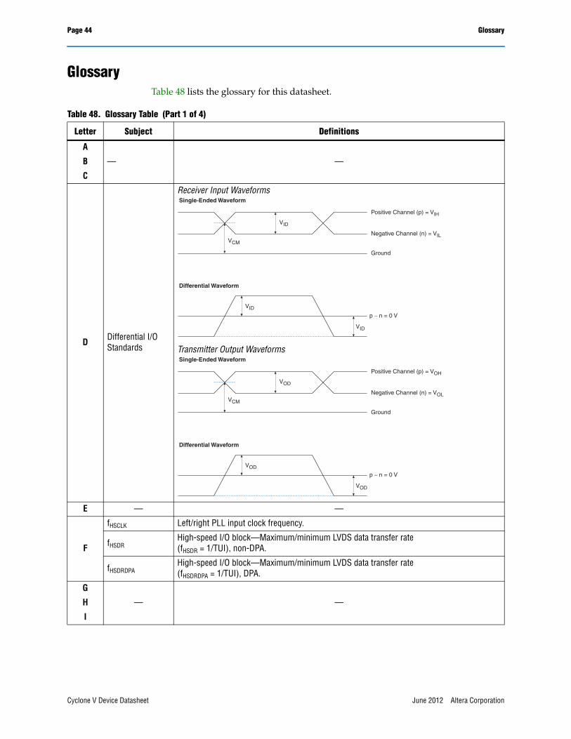
Page 44 Glossary
GlossaryTable 48 lists the glossary for this datasheet.
Table 48. Glossary Table (Part 1 of 4)
Letter Subject Definitions
A
B
C
— —
D Differential I/O Standards
Receiver Input Waveforms
Transmitter Output Waveforms
E — —
F
fHSCLK Left/right PLL input clock frequency.
fHSDRHigh-speed I/O block—Maximum/minimum LVDS data transfer rate (fHSDR = 1/TUI), non-DPA.
fHSDRDPAHigh-speed I/O block—Maximum/minimum LVDS data transfer rate (fHSDRDPA = 1/TUI), DPA.
G
H
I
— —
Single-Ended Waveform
Differential Waveform
Positive Channel (p) = VIH
Negative Channel (n) = VIL
Ground
VID
VID
VID
p − n = 0 V
VCM
Single-Ended Waveform
Differential Waveform
Positive Channel (p) = VOH
Negative Channel (n) = VOL
Ground
VOD
VOD
VOD
p − n = 0 V
VCM
Cyclone V Device Datasheet June 2012 Altera Corporation

Glossary Page 45
J
J High-speed I/O block—Deserialization factor (width of parallel data bus).
JTAG Timing Specifications
JTAG Timing Specifications:
K
L
M
N
O
— —
P
PLL Specifications
Diagram of PLL Specifications (1)
Note:
(1) Core Clock can only be fed by dedicated clock input pins or PLL outputs.
Preliminary
Some tables show the designation as “Preliminary”. Preliminary characteristics are created using simulation results, process data, and other known parameters.
Final numbers are based on actual silicon characterization and testing. The numbers reflect the actual performance of the device under worst-case silicon process, voltage, and junction temperature conditions. There are no preliminary designations on finalized tables.
Q — —
R RL Receiver differential input discrete resistor (external to the Cyclone V device).
Table 48. Glossary Table (Part 2 of 4)
Letter Subject Definitions
TDO
TCK
tJPZX tJPCO
tJPH
t JPXZ
tJCP
tJPSU t JCL tJCH
TDI
TMS
Core Clock
External FeedbackReconfigurable in User Mode
Key
CLK
NPFD
Switchover
Delta Sigma Modulator
VCOCP LF
CLKOUT Pins
GCLK
RCLK
fINPFDfINfVCO fOUT
fOUT_EXT
Counters C0..C17
4
June 2012 Altera Corporation Cyclone V Device Datasheet

Page 46 Glossary
S
Sampling window (SW)
Timing Diagram—the period of time during which the data must be valid in order to capture it correctly. The setup and hold times determine the ideal strobe position within the sampling window, as shown:
Single-ended voltage referenced I/O standard
The JEDEC standard for the SSTL and HSTL I/O defines both the AC and DC input signal values. The AC values indicate the voltage levels at which the receiver must meet its timing specifications. The DC values indicate the voltage levels at which the final logic state of the receiver is unambiguously defined. After the receiver input has crossed the AC value, the receiver changes to the new logic state.
The new logic state is then maintained as long as the input stays beyond the AC threshold. This approach is intended to provide predictable receiver timing in the presence of input waveform ringing, as shown:
Single-Ended Voltage Referenced I/O Standard
T
tC High-speed receiver/transmitter input and output clock period.
TCCS (channel-to-channel-skew)
The timing difference between the fastest and slowest output edges, including the tCO variation and clock skew, across channels driven by the same PLL. The clock is included in the TCCS measurement (refer to the Timing Diagram figure under SW in this table).
tDUTY
High-speed I/O block—Duty cycle on high-speed transmitter output clock.
Timing Unit Interval (TUI)
The timing budget allowed for skew, propagation delays, and the data sampling window.(TUI = 1/(Receiver Input Clock Frequency Multiplication Factor) = tC/w)
tFALL Signal high-to-low transition time (80-20%)
tINCCJ Cycle-to-cycle jitter tolerance on the PLL clock input
tOUTPJ_IO Period jitter on the general purpose I/O driven by a PLL
tOUTPJ_DC Period jitter on the dedicated clock output driven by a PLL
tRISE Signal low-to-high transition time (20–80%)
U — —
Table 48. Glossary Table (Part 3 of 4)
Letter Subject Definitions
Bit Time
0.5 x TCCS RSKM Sampling Window (SW)
RSKM 0.5 x TCCS
VIH(AC)
VIH(DC)
VREFVIL(DC)
VIL(AC)
VOH
VOL
VCCIO
VSS
Cyclone V Device Datasheet June 2012 Altera Corporation

Glossary Page 47
V
VCM(DC) DC common mode input voltage.
VICM Input common mode voltage—The common mode of the differential signal at the receiver.
VIDInput differential voltage swing—The difference in voltage between the positive and complementary conductors of a differential transmission at the receiver.
VDIF(AC) AC differential input voltage—Minimum AC input differential voltage required for switching.
VDIF(DC) DC differential input voltage— Minimum DC input differential voltage required for switching.
VIHVoltage input high—The minimum positive voltage applied to the input which is accepted by the device as a logic high.
VIH(AC) High-level AC input voltage
VIH(DC) High-level DC input voltage
VILVoltage input low—The maximum positive voltage applied to the input which is accepted by the device as a logic low.
VIL(AC) Low-level AC input voltage
VIL(DC) Low-level DC input voltage
VOCMOutput common mode voltage—The common mode of the differential signal at the transmitter.
VODOutput differential voltage swing—The difference in voltage between the positive and complementary conductors of a differential transmission at the transmitter.
VSWING Differential input voltage
VX Input differential cross point voltage
VOX Output differential cross point voltage
W W High-speed I/O block—Clock Boost Factor
X
Y
Z
— —
Table 48. Glossary Table (Part 4 of 4)
Letter Subject Definitions
June 2012 Altera Corporation Cyclone V Device Datasheet
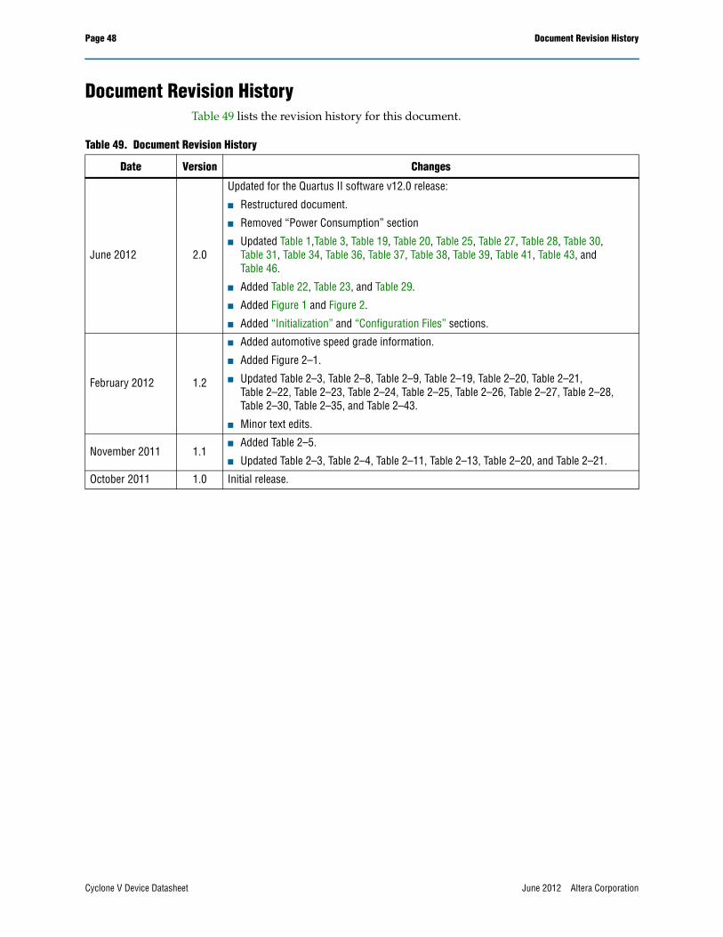
Page 48 Document Revision History
Document Revision HistoryTable 49 lists the revision history for this document.
Table 49. Document Revision History
Date Version Changes
June 2012 2.0
Updated for the Quartus II software v12.0 release:
■ Restructured document.
■ Removed “Power Consumption” section
■ Updated Table 1,Table 3, Table 19, Table 20, Table 25, Table 27, Table 28, Table 30, Table 31, Table 34, Table 36, Table 37, Table 38, Table 39, Table 41, Table 43, and Table 46.
■ Added Table 22, Table 23, and Table 29.
■ Added Figure 1 and Figure 2.
■ Added “Initialization” and “Configuration Files” sections.
February 2012 1.2
■ Added automotive speed grade information.
■ Added Figure 2–1.
■ Updated Table 2–3, Table 2–8, Table 2–9, Table 2–19, Table 2–20, Table 2–21, Table 2–22, Table 2–23, Table 2–24, Table 2–25, Table 2–26, Table 2–27, Table 2–28, Table 2–30, Table 2–35, and Table 2–43.
■ Minor text edits.
November 2011 1.1■ Added Table 2–5.
■ Updated Table 2–3, Table 2–4, Table 2–11, Table 2–13, Table 2–20, and Table 2–21.
October 2011 1.0 Initial release.
Cyclone V Device Datasheet June 2012 Altera Corporation