Vlsi Notes
91
Design of High Speed CMOS Logic Networks (Chapter 8 of John.P.Uyemura and Chapter5 of EC74) In VLSI technology, switching speed of logic circuits is an important parameter and is closely related to the timing specifications. Modern CMOS technology is capable of fabricating MOSFETS with channel lengths smaller than 65 nm. Here, the aspect ratio (W/L) is the important critical parameter in high speed CMOS logic networks. Gate delays:Gate delay is defined as the time taken by the Logic gate to respond to the signal given at its input. As shown in fig.1, the NAND gate takes a fixed duration to give the output after the input is given. This time is the gate delay. The parameters associated with the gate delay are transistor resistance, Capacitance and the load capacitance, C L . Fig.2 illustrates the variation of the gate delay for different values of C L . 0 U1A 7400 1 2 3 Fig.1 Circuit to illustrate the definition of Fig.2 Graph of delay time v/s load of gate delay capacitance FET unit Resistance is given by ( ) T DD u V V L W k R − ⎟ ⎠ ⎞ ⎜ ⎝ ⎛ = ' 1 Where is unit transistor Resistance, W and L are the width and Length of the transistor, K’ is Ru ox n C μ u S Sm u D Dm Gu Gm u m mC C mC C mC C m R R = = = = , , , VLSI circuits - Prof.M.J.Shanthi Prasad, HOD of E & C, BIT, Bangalore B Vout 0 0 A CL 1n Vdd 3.3Vdc
Transcript of Vlsi Notes

Design of High Speed CMOS Logic Networks (Chapter 8 of John.P.Uyemura and Chapter5 of EC74)
In VLSI technology, switching speed of logic circuits is an important parameter
and is closely related to the timing specifications. Modern CMOS technology is capable of fabricating MOSFETS with channel lengths smaller than 65 nm. Here, the aspect ratio (W/L) is the important critical parameter in high speed CMOS logic networks. Gate delays:Gate delay is defined as the time taken by the Logic gate to respond to the signal given at its input. As shown in fig.1, the NAND gate takes a fixed duration to give the output after the input is given. This time is the gate delay. The parameters associated with the gate delay are transistor resistance, Capacitance and the load capacitance, CL. Fig.2 illustrates the variation of the gate delay for different values of CL.
0
U1A
7400
1
23
Fig.1 Circuit to illustrate the definition of Fig.2 Graph of delay time v/s load of gate delay capacitance
FET unit Resistance is given by
( )TDD
u
VVLWk
R−⎟
⎠⎞
⎜⎝⎛
='
1
Where is unit transistor Resistance, W and L are the width and Length of the
transistor, K’ is
Ru
oxnCμ uSSmuDDmGuGmu
m mCCmCCmCCmR
R ==== ,,,
VLSI circuits - Prof.M.J.Shanthi Prasad, HOD of E & C, BIT, Bangalore
B Vout
0
0ACL
1n
Vdd3.3Vdc

- 2 -
uWW =min Fig.3 Minimum-Size FET Fig.4 3X Scaled- FET
Fig.3 shows the layout of FET and Fig.4 shows the scaled FET, 3 times the original size. The parasitic capacitances for unit size FET are given by
uSBGSSu
uDBGDDu
uOXGu
CCCCCC
WLCC
)()(
)(
+=+=
=
where CGu, CDu and Csu are the Gate, Drain and Source Capacitances. The width of unit size FET is the minimum size given by Wmin = Wu. Fig.4 shows the scaled FET with m = 3. The aspect ratio becomes 3 times the unit FET and the aspect ratio also become e times unit FET. In general, the size of scaled FETs are integer multiples of the minimum
uLW
LW
⎟⎠⎞
⎜⎝⎛=⎟
⎠⎞
⎜⎝⎛ 3
3
( ) uWW 33 =
The FET parasitic resistance and capacitance becomes uSSuuDDuGuGuuu mCCmCCmCCmRR ==== ,,,
VLSI circuits - Prof.M.J.Shanthi Prasad, HOD of E & C, BIT, Bangalore
2

- 3 -
It can be seen from the above expressions that, the capacitances are increased 3 times and the resistance is decreased by 3 times. But, an important observation is that, the RC product remains same RmCm=RuCu. The Resistance and capacitance of 3X FET of fig.4 is given by
uSSxuDDxGuGxu CCCCCCRRx 3,3,3,3 ====
HLf
LHr
tttt
==
uSS
uDD
GuG
u
CCCCCC
RR
3333
3
3
3
3
=
==
=
The rise time and fall time of 3X FET are given by
3
3
3
3
Lun
fof
Lpu
ror
Ctt
Ctt
α
α
+=
+=
If we connect the minimum size FET for both PMOS and NMOS as shown in Fig.5, results in an inverter. The layout of the inverter is shown in Fig.6.
M2
V13.3Vdc
0
M1
0
in out
Fig.5 Schematic diagram of Inverter Fig.6 Layout of Inverter VLSI circuits - Prof.M.J.Shanthi Prasad, HOD of E & C, BIT, Bangalore
3

- 4 -
Steps that has to be followed in drawing the layout of an inverter: To make NMOS FET, n+ layer has to be placed on p-type substrate. A poly layer
in between the n+ layer completes the NMOSFET. This is shown in the bottom of fig.6. The drain, gate and source are indicated by Dn, Gn and Sn.
To make PMOS FET, p+ layer has to be placed on p-type substrate. A poly layer in between the p+ layer completes the PMOSFET. This is shown in the top of fig.6. The drain, gate and source are indicated by Dp, Gp and Sp.
The metal1 layer has to be placed to get contact with the active layer and the p+ layer. The n-well has to be placed surrounding the p+ layer. The Cell layers used during the layout of VLSI circuits are shown in fig.7. The Text book by VLSI Design by Plucknell gives the details of cell layers and layouts for various logic circuits. Students can practice these by drawing the layouts in sketch pens. It is advisable to learn them by drawing the layouts by using any of the EDA tool.
Fig.7 Cell layers in VLSI Circuits Lambda Based Rules
While drawing the layouts of VLSI circuits, Design rules has to be followed. Some of them has been narrated in fig.8 and it states that, 1) The width of n+/p+ diffusion should be of minimum width 2l and the gap between two diffusions should also be 2λ.
Fig.8 Diagrams to illustrate the Lambda Based Rules
4

- 5 -
VLSI circuits - Prof.M.J.Shanthi Prasad, HOD of E & C, BIT, Bangalore 2) The gap between diffusion and the poly has to be of minimum width λ. 3) The width of metal1 should be of minimum width 3λ and the gap between two metal1’s should be 4λ and similar other rules has to be followed while drawing the layouts in VLSI circuits. Cell Concepts: The basic building block s in physical design are called cells. A cell may be as simple as an FET, or as complex as an arithmetic logic unit (ALU). The basic cells of inverter, NAND2, and a cell consisting of inverter, NAND2 and one more inverter at the output are shown in fig.9. Also the complex cell showing only the inputs and output have been narrated. This is the usefulness of the cell concept. This becomes useful in writing VHDL code in behavioral mode. Fig.9 Diagrams to illustrate the Concept of cells
in
B
Gnd
New Complex Cell
7406
1 2
U5A
7428
2
31
U4A
7400
1
23
U2A
7400
1
23
A
U3A
7406
1 2
XNAND2
in2Gnd
out
XNOT
Vdd
B
Vdd
C
Vdd
Gnd
Vdd
out
in1
Primitive Cells
out
U6A
7428
2
31
Gnd
C
Vdd
outA
NAND2 Gate Scaling
0V
0V
M3
IRF150
M2
IRF9140
0
M1
IRF9140
0
0
10.00V
0V
VA
TD = 0US
TF = 0.1USPW = 1UsPER = 2Us
V1 = 0v
TR = 0.1us
V2 = 10v
M4
IRF150
5.000V
0V
0VB
TD = 0US
TF = 0.1USPW = 0.5UsPER = 1Us
V1 = 0v
TR = 0.1us
V2 = 10v
R1
47K
0
V110V
10.00V
0V
Fig.10 Fig.11 Fig.12 Schematic Diagram Layout using unit size FET Layout using 3X Scaled FET
Switching Equations Compared to the switching equations of the inverter, NAND2 gate switching equations gets modified.
VLSI circuits - Prof.M.J.Shanthi Prasad, HOD of E & C, BIT, Bangalore
5

- 6 -
This is because, tr0 and tf0 are proportional to the product of Ru and CFET. In the inverter, two FETs contribute to the capacitance. But, in NAND2 gate, there are 3 FETs that touch the output node, so a factor of 3/2 has to be introduced. The Resistances scale in a different manner. The pFET resistance Rp is the same as that for an inverter, while the nFET Resistance Rn between the output node and the ground is doubled because of the series connection. The switching equations for unit NAND2 gate are
2323
Lunfof
Lpuror
Ctt
Ctt
α
α
+=
+⎟⎠⎞
⎜⎝⎛=
If we scale the FETs with m = 3, then α factors are reduced by 1/m because of the decrease in Resistance. The decrease in resistance counteracts the in crease in CFET, so that the zero-load terms are unchanged. Thus, the switching equations for m-scaled NAND2 gate and for an N-input NAND2 gate using m-scaled FETs becomes
3
23
323
Lun
fof
Lpu
ror
Ctt
Ctt
⎟⎠
⎞⎜⎝
⎛+=
⎟⎟⎠
⎞⎜⎜⎝
⎛+⎟
⎠⎞
⎜⎝⎛=
α
α
3
)1(
21
Lun
fof
Lpu
ror
CN
tNt
Cm
tNt
⎟⎠
⎞⎜⎝
⎛++=
⎟⎟⎠
⎞⎜⎜⎝
⎛+⎟
⎠⎞
⎜⎝⎛ +
=
α
α
Analysis of NOR2 gate can be analyzed in a similar manner. The switching equations for m-scaled NAND2 gate and for an N-input NAND2 gate using m-scaled FET’s becomes
23
23
Lunfof
Lpuror
Ctt
Ctt
α
α
+⎟⎠⎞
⎜⎝⎛=
+=
2
1
)1(
Lun
fof
Lpu
ror
Cm
tNt
Cm
NtNt
⎟⎠
⎞⎜⎝
⎛+⎟⎠⎞
⎜⎝⎛ +
=
⎟⎟⎠
⎞⎜⎜⎝
⎛++=
α
α
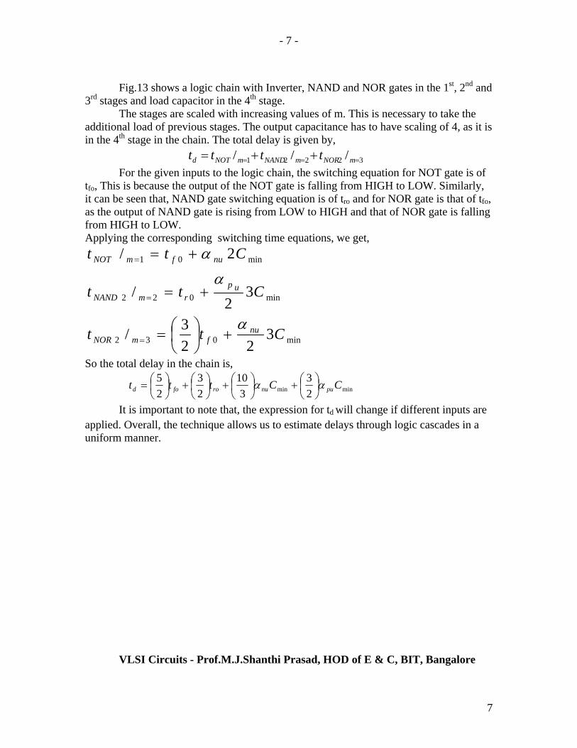
The above switching equations clearly demonstrate the dependence on the number of inputs (N) and the FET Scaling factor (m). Delay time: The above technique of gate design provides a structured approach for estimating delays. Fig.13 shows a logic chain with M-stages, the total delay, td is given
by the summation of individual delays. Mathematically, ∑=
=M
iid tt
1
Fig.13 Example for
Delay time
C= 4 Cminin
10 2
311
23
1 2
C1C2
C30
VLSI Circuits - Prof.M.J.Shanthi Prasad, HOD of E & C, BIT, Bangalore
6
- 7 -
Fig.13 shows a logic chain with Inverter, NAND and NOR gates in the 1st, 2nd and
3rd stages and load capacitor in the 4th stage. The stages are scaled with increasing values of m. This is necessary to take the
additional load of previous stages. The output capacitance has to have scaling of 4, as it is in the 4th stage in the chain. The total delay is given by,
32221 /// === ++= mNORmNANDmNOTd tttt For the given inputs to the logic chain, the switching equation for NOT gate is of
tfo, This is because the output of the NOT gate is falling from HIGH to LOW. Similarly, it can be seen that, NAND gate switching equation is of tro and for NOR gate is that of tfo, as the output of NAND gate is rising from LOW to HIGH and that of NOR gate is falling from HIGH to LOW. Applying the corresponding switching time equations, we get,
min032
min022
min01
322
3/
32
/
2/
Ctt
Ctt
Ctt
nufmNOR
uprmNAND
nufmNOT
α
α
α
+⎟⎠⎞
⎜⎝⎛=
+=
+=
=
=
=
So the total delay in the chain is,
minmin 23
310
23
25 CCttt punurofod αα ⎟
⎠⎞
⎜⎝⎛+⎟
⎠⎞
⎜⎝⎛+⎟
⎠⎞
⎜⎝⎛+⎟
⎠⎞
⎜⎝⎛=
It is important to note that, the expression for td will change if different inputs are applied. Overall, the technique allows us to estimate delays through logic cascades in a uniform manner.
VLSI Circuits - Prof.M.J.Shanthi Prasad, HOD of E & C, BIT, Bangalore
7

- 8 -
Solutions to problems in Design of High speed CMOS Logic circuits 7th chapter of John P.Uyemura: 7.1 Given Data:
VDD = 3.3V VTP = -0.8V VTn = 0.6V Kn’ = 100 μA/V2 Kp’ == 42 μA/V2 To find VM From Eqn.6.109
2' /100010100 VAx
LWk
nnn μβ ==⎟
⎠⎞
⎜⎝⎛=
2' /5881442 VAx
LWk
ppp μβ ==⎟
⎠⎞
⎜⎝⎛=
From Equation 7.14
V
xVVV
V
p
n
p
nTnTPDD
M 358.1
58810001
58810007.08.03.3
1
//
=⎟⎟⎟⎟
⎠
⎞
⎜⎜⎜⎜
⎝
⎛
+
+−=
⎟⎟⎟⎟⎟
⎠
⎞
⎜⎜⎜⎜⎜
⎝
⎛
+
+−
=
ββ
ββ
VM = 1.358 V 7.2 Given Data: VDD = 3 V VTP = -0.82 V VTn = 0.6 V VM = 1.3 V
To find p
n
ββ
From Equation 7.14
V
xxVVV
V
p
n
p
n
p
n
p
nTnTPDD
M 3.11
6.082.03
1
//
=
⎟⎟⎟⎟⎟
⎠
⎞
⎜⎜⎜⎜⎜
⎝
⎛
+
+−
=
⎟⎟⎟⎟⎟
⎠
⎞
⎜⎜⎜⎜⎜
⎝
⎛
+
+−
=
ββ
ββ
ββ
ββ
p
n
ββ
= 1.580
VLSI Circuits - Prof.M.J.Shanthi Prasad, HOD of E & C, BIT, Bangalore
8

- 9 -
7.3 VDD = 5 V VTP = -0.7 V VTn = 0.6 V
2/1.2 VAn μβ = 2/8.1 VAp μβ =
a) To find VM
From Equation 7.14
V
xVVV
V
p
n
p
nTnTPDD
M 378.2
8.11.21
8.11.26.07.05
1
//
=⎟⎟⎟⎟
⎠
⎞
⎜⎜⎜⎜
⎝
⎛
+
+−=
⎟⎟⎟⎟⎟
⎠
⎞
⎜⎜⎜⎜⎜
⎝
⎛
+
+−
=
ββ
ββ
VM = 2.378 V b) To find Rn and Rp From Equation 7.28
( ) ( ) Ω=⎟⎟⎠
⎞⎜⎜⎝
⎛−
=⎟⎟⎠
⎞⎜⎜⎝
⎛−
= 1086.051.2
11
TnDDnn VV
Rβ
( ) ( ) Ω=⎟⎟⎠
⎞⎜⎜⎝
⎛−
=⎟⎟⎠
⎞⎜⎜⎝
⎛
−= 129
/7.0/58.11
//1
TpDDpp VV
Rβ
c) To find tr and tf When CL = 0 From Equation 7.52 pft τ2.2= From Equation 7.32 fFCCCCR FETLoutoutpp 74740, =+=+==τ
psxxxtr 03.2110741292.2 15 == − From Equation 7.48 nft τ2.2= From Equation 7.32 fFCCCCR FETLoutoutnn 74740, =+=+==τ
psxxxt f 582.1710741082.2 15 == − d) To find tr and tf When CL = 115fF From Equation 7.52 prt τ2.2= From Equation 7.32 fFCCCCR FETLoutoutpp 18974115, =+=+==τ
psxxxtr 638.53101891292.2 15 == − VLSI Circuits - Prof.M.J.Shanthi Prasad, HOD of E & C, BIT, Bangalore
9

- 10 -
From Equation 7.48 nft τ2.2= From Equation 7.32 fFCCCCR FETLoutoutnn 18974115, =+=+==τ
psxxxt f 9.44101891082.2 15 == − e) To plot tr v/s CL and tf v/s CL Sl.no. CL in fF tr in ps tf in ps
1 0 21.03 17.582 2 30 29.515 24.71 3 60 38.029 31.838 4 90 46.543 38.966 5 115 53.638 44.9
Rise time V/S <>Load Capacitance
0204060
1 2 3 4 5
Load Capacitance
Ris
e tim
e
fall time V/S Load Capacitance
0204060
1 2 3 4 5
Load Capacitance
Fall
time
7.4 Given Data: VDD = 5 V VTP = -0.7V VTn = 0.6V Kn’ = 150 μA/V2 Kp’ == 60 μA/V2 To find VM, From Eqn.6.109
2' /600
14150 VAx
LWk
nnnn μβ =⎟
⎠⎞
⎜⎝⎛=⎟
⎠⎞
⎜⎝⎛=
2' /480
1842 VAx
LWk
pppp μβ =⎟
⎠⎞
⎜⎝⎛=⎟
⎠⎞
⎜⎝⎛=
VLSI Circuits - Prof.M.J.Shanthi Prasad, HOD of E & C, BIT, Bangalore
10

- 11 -
From Equation 7.14
V
xVVV
V
p
n
p
nTnTPDD
M 244.2
4806001
4806006.07.05
1
//
=⎟⎟⎟⎟
⎠
⎞
⎜⎜⎜⎜
⎝
⎛
+
+−=
⎟⎟⎟⎟⎟
⎠
⎞
⎜⎜⎜⎜⎜
⎝
⎛
+
+−
=
ββ
ββ
VM = 2.244 V 7.5 Given Data VDD = 5V VTP = -0. VTn = 0.6V Kn’ = 150 μA/V2 Kp’ == 60 μA/V2 From Eqn.6.109
2' /750
8.04150 VAx
LWk
nnn μβ =⎟
⎠⎞
⎜⎝⎛=⎟
⎠⎞
⎜⎝⎛=
2' /600
8.0460 VA
LWk
ppp μβ =⎟
⎠⎞
⎜⎝⎛=⎟
⎠⎞
⎜⎝⎛=
a) To find Cin
From Equation 6.115 ( ) ( ) F28.178.087.2 fxWLCC poxGP === ( ) ( ) F64.88.047.2 fxWLCC noxGn ===
From Equation 7.30 Cin = CGn + CGP = 25.72 fF b) To find Rn and Rp From Equation 7.28
( ) ( ) Ω=⎟⎟⎠
⎞⎜⎜⎝
⎛−
=⎟⎟⎠
⎞⎜⎜⎝
⎛−
= − 3036.0510750
116 xxVV
RTnDDn
n β
( ) ( ) Ω=⎟⎟⎠
⎞⎜⎜⎝
⎛−
=⎟⎟⎠
⎞⎜⎜⎝
⎛
−= 387
/7.0/56001
//1
TpDDpp VV
Rβ
c) To find tr and tf From Equation 7.52 pft τ2.2= From Equation 7.32 FETLoutoutpp CCCCR +== ,τ VLSI Circuits - Prof.M.J.Shanthi Prasad, HOD of E & C, BIT, Bangalore
11

- 12 -
From Equation 7.33, CFET = CDp + CDn From Equation 7.29, CDp = Cp + CGp/2 From Equation 6.92, Cp = Cjp Abot+ Cjspw Psw, Psw = 2(W+X) Cp = Cjp Abot + Cjspw Psw = 1.05 x 8 x 2.1 + 0.32 x 2(8 + 2.1) = 24.1 fF CDp = Cp + CGp/2 = 24.1 + 17.28/2 = 32.74 fF Similarly, Cn = Cjn Abot + Cjsnw Psw = 0.86 x 8 x 2.1 + 0.24 x 2(4 + 2.1) = 10.15 fF CDn = Cn + CGn/2 = 10.15 + 8.64/2 = 14.47 fF ∴CFET = CDp + CDn = 32.74 + 14.47 = 47.21 fF tr = 2.2 x Rp (CL + CFET) = 2.2 x 387 (80 + 47.21) = 84.724 ps tf = 2.2 x Rn (CL + CFET) = 2.2 x 303 (80 + 47.21) = 108.212 ps 7.7 Given Data: VDD = 5 V VTP = -0.7 V VTn = 0.6 V βn = 2βp
From Equation 7.95, Mid-point voltage of NAND2 gate is
V
x
xx
xN
xN
xVVV
V
p
p
p
p
p
n
p
nTnTPDD
M 523.22
211
2216.07.05
11
1//
=
⎟⎟⎟⎟⎟⎟
⎠
⎞
⎜⎜⎜⎜⎜⎜
⎝
⎛
+
+−
=
⎟⎟⎟⎟⎟
⎠
⎞
⎜⎜⎜⎜⎜
⎝
⎛
+
+−
=
ββ
ββ
ββ
ββ
VM = 2.523 V 7.8 Given Data: VDD = 3.3 V VTP = -0.8 V VTn = 0.65 V βp = 2.2βn
From Equation 7.98, Mid-point voltage of NOR2 gate is
Vx
xx
Nx
xNxVVV
V
n
n
n
n
p
n
p
nTnTPDD
M 438.1
2.221
2.2265.08.03.3
1
//
=
⎟⎟⎟⎟⎟
⎠
⎞
⎜⎜⎜⎜⎜
⎝
⎛
+
+−=
⎟⎟⎟⎟⎟
⎠
⎞
⎜⎜⎜⎜⎜
⎝
⎛
+
+−
=
ββ
ββ
ββ
ββ
VM = 1.438 V VLSI Circuits - Prof.M.J.Shanthi Prasad, HOD of E & C, BIT, Bangalore
12

- 13 -
7.9 Given Data: VDD = 5 V (W/L)n = 4 Kn’ = 120 μA/V2 VTn = 0.55 V VM = 2.4 V VTp = -0.9 V To find βp
2' /480
14120 VAx
LWk
nnnn μβ =⎟
⎠⎞
⎜⎝⎛=⎟
⎠⎞
⎜⎝⎛=
From Equation 7.95, Mid-point voltage of NAND3 gate is
Vx
xx
xN
xN
xVVV
V
p
p
p
n
p
nTnTPDD
M 4.2480
311
4803155.09.05
11
1//
=
⎟⎟⎟⎟⎟
⎠
⎞
⎜⎜⎜⎜⎜
⎝
⎛
+
+−
=
⎟⎟⎟⎟⎟
⎠
⎞
⎜⎜⎜⎜⎜
⎝
⎛
+
+−
=
β
β
ββ
ββ
Solving, βp = 60 μA/V2 7.10 Given Data: Cout = 130 fF C1 = 36 fF C2 = 36 fF βn = 2 mA/V2 VDD = 3.3 V VTn = 0.7 V From Equation 7.28
( ) ( ) Ω=⎟⎟⎠
⎞⎜⎜⎝
⎛−
=⎟⎟⎠
⎞⎜⎜⎝
⎛−
= − 1927.03.3102
113 xxVV
RTnDDn
n β
a) Applying the Elmore formula as illustrated in page 268 of Uyemura, we get the discharge circuit and the discharge time constant for fig.P7.1,
( ) ( ) ( nnnnnnoutn RCRRCRRRC 12 )+++++=τ( ) ( ) ( ) psxx nnn 216.95192361922361923130 =++=τ Vout
C1
0
0
0
Cout
0
Vout
C2Rn
Rn
Rn
VLSI Circuits - Prof.M.J.Shanthi Prasad, HOD of E & C, BIT, B’lore
13

- 14 -
b) ( ) psxxRRRC nnnoutn 88.741923130 ==++=τ ( ) ( )
( ) %16.27%100a
ba =error %n
nn =− x
τττ
0
Vout
Rn
0
Rn
VoutCout
Rn
7.11 The logical circuit for the Boolean expression, edcbaf ... += is given by
M2 b
0
a
M1
0
e
M1
V13.3Vdc
c
0
M2 M2
M1
M1
e
0
0
0
M2
M1
d
d
b 0
a
M2
f
VLSI Circuits - Prof.M.J.Shanthi Prasad, HOD of E & C, BIT, Bangalore
14

- 15 -
7.12 The logical circuit for the Boolean expression, ( ) XWZYXf ++= is given by
Y
M2
0
M1
Z
0
M1
V13.3Vdc
X
0
M2
MbreakP
W
M2
MbreakP
M1 M1
Y
0
0
M2
M1
Z
W
0
M2
X X
0
X
f
VLSI Circuits - Prof.M.J.Shanthi Prasad, HOD of E & C, BIT, Bangalore
15
- 16 -
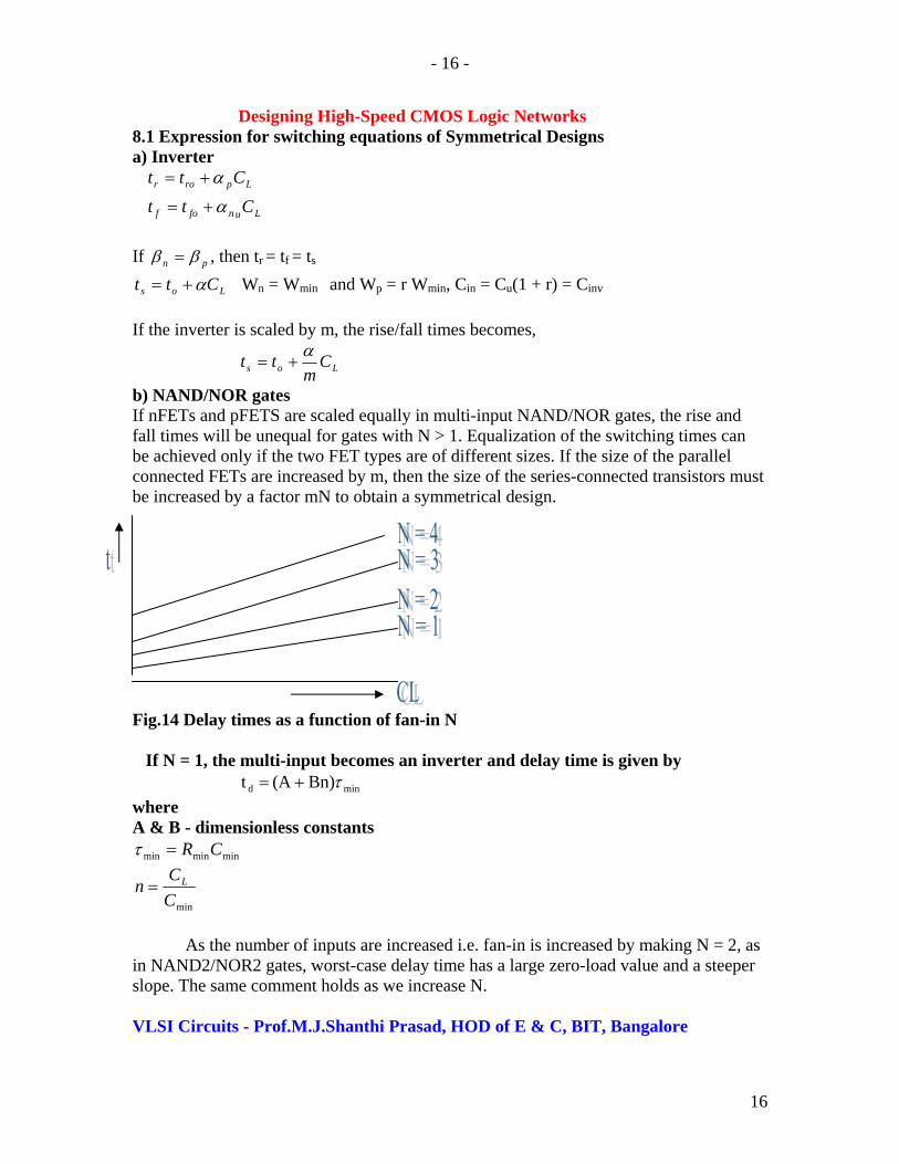
Designing High-Speed CMOS Logic Networks 8.1 Expression for switching equations of Symmetrical Designs a) Inverter
Lunfof
Lpror
Ctt
Ctt
α
α
+=
+=
If pn ββ = , then tr = tf = ts
Los Ctt α+= Wn = Wmin and Wp = r Wmin, Cin = Cu(1 + r) = Cinv
If the inverter is scaled by m, the rise/fall times becomes,
Los Cm
tt α+=
b) NAND/NOR gates If nFETs and pFETS are scaled equally in multi-input NAND/NOR gates, the rise and fall times will be unequal for gates with N > 1. Equalization of the switching times can be achieved only if the two FET types are of different sizes. If the size of the parallel connected FETs are increased by m, then the size of the series-connected transistors must be increased by a factor mN to obtain a symmetrical design. Fig.14 Delay times as a function of fan-in N If N = 1, the multi-input becomes an inverter and delay time is given by Bn) (A t mind τ+= where A & B - dimensionless constants
minminmin CR=τ
minCCn L=
As the number of inputs are increased i.e. fan-in is increased by making N = 2, as
in NAND2/NOR2 gates, worst-case delay time has a large zero-load value and a steeper slope. The same comment holds as we increase N.
VLSI Circuits - Prof.M.J.Shanthi Prasad, HOD of E & C, BIT, Bangalore
16

- 17 -
An empirical fit may be obtained by including a factor x1 in the formula as follows.
( ) Bn) (A t min1
1 N,d τ+= −Nx For Example, if the increase from N = 1 to N = 2 is 17% per
input, this means that, x1 = 1.17 and ( ) Bn) (A 17.1t min
1 N,d τ+= −N
If the FETs are scaled by a factor m = 1, 2, . . .. , then the delay time expression modifies to
( ) n)mB (A t min
11 N,d
m τ+= −Nx
For a complex N-input logic gate, the charging and discharging times will increase further by 5 to 20% and we can account that by including one more empirical fitting parameter x2 >1, to obtain
( ) n)mB (A t min
112 N,d
m τ+= −Nxx
Applying these formulae to the logic chain of Fig.15, the 3 switching equations becomes
0 Fig.15 An example of a Logic chain
min1 )2(! tBAt mNOT +==
min13/2
min12/2
42
32
tBAxt
tBAxt
mNOR
mNAND
⎟⎠⎞
⎜⎝⎛ +=
⎟⎠⎞
⎜⎝⎛ +=
=
=
Rearranging, we get
( ) BxAxttd
⎥⎦
⎤⎢⎣
⎡+⎟
⎠⎞
⎜⎝⎛++= 2
271 11
min
VLSI Circuits - Prof.M.J.Shanthi Prasad, HOD of E & C, BIT, Bangalore
C= 4 Cminin
12
311
23
1 2
C2C3
C1 0
32221 !!! === ++= mNORmNANDmNOTd tttt
17

- 18 -
if x1=1.17, BAttd 1.617.2min
+=
is the delay compared to a single inverter. It may be noted from equation 8.32 that,
the delay of a single inverter is BAttd +=min
In general, the design of high speed logic CMOS logic networks is done by using different algorithms and different types of logic cascade. This provides a basis for deciding on the design that will be the fastest. Driving Large Capacitive loads As the analysis of inverter circuits is the basis for high-speed design and as the analysis can be extended to other logic gates, an inverter circuit has been considered here.
VCC
LoadVout
0
Vin
M1
MbreakP
CLM2
MbreakN
Fig.16 CMOS Inverter Circuit Fig.16 shows the inverter circuit. βn = βp =β (Assumed symmetric circuit)
∴np L
WrLW
⎟⎠⎞
⎜⎝⎛=⎟
⎠⎞
⎜⎝⎛
where r is the ratios of mobility given by
1''>⎟
⎟⎠
⎞⎜⎜⎝
⎛=⎟
⎟⎠
⎞⎜⎜⎝
⎛=
p
n
p
n
kk
rμμ
( )TDDpn VV
RRR−
===β
1
This design yields a voltage transfer characteristic (VTC) with a midpoint voltage of VM=VDD/2 and equal rise and fall times. For a 0-to-1 transition at the output, the output voltage across CL is of the form,
[ ]τ/1)( tDDout eVtV −−=
VLSI Circuits - Prof.M.J.Shanthi Prasad, HOD of E & C, BIT, Bangalore
18

- 19 -
while a 1-to-0 change is described by
τ/)( tDDout eVtV −=
where τ is the time constant given by
( )LFETout CCRRC +==τ The rise/fall time equation becomes ts = tr = tf =to+αCL
where to is the delay time with zero-load. to is invariant to changes in the circuit and α ∝ R. R is dependent on β, the transient response requirements can b e met by adjusting β. β can be adjusted during the device design and before sending to fab. Unit load: The load is said to be of unit value, if the gate’s load capacitance is the same as the gate’s own input capacitance. This situation exists, if the inverter of fig.16 is driving the symmetrical inverter as shown in fig.17. Cin = CGn + CGp = Cox(AGn+AGp) = CoxL(Wn + Wp) = (1 +r)(CoxLWn) = (1 + r) CGn Where AGn and AGp are the gate areas of the respective devices.
VCC
M2
MbreakN
Vout
VCC
Vin
M1
MbreakP
M1
MbreakP
M2
MbreakN
Cin
Fig.17 Circuit to illustrate the concept of Unit Load As CL Cin ts . To keep ts small, α can be decreased. But as α W R . But increasing the value of β compensates for the larger load and demonstrates the speed-versus-area trade-off. If the aspect ratio is increased by scaling, β increases. i.e. β’ = S β, R’ = R/S and α’ = α/S, C’in = SCin and W’n = SWn Then the switching time equation becomes,
ts = tr = tf =to+(α/S)CL VLSI Circuits - Prof.M.J.Shanthi Prasad, HOD of E & C, BIT, Bangalore
19

- 20 -
If CL = SCin as in Fig.18, then the switching time is the same as for a unit load. Thus the compensation factor (1/S) allows us to drive larger CL.
VCC
Driving Stage
M2
MbreakN
CL large
Cin,d
VCC
VinBeeta large
M1
MbreakP
Beeta large
M1
MbreakP
Beeta large
M2
MbreakN
CL,d=Cin
Fig.18 Inverter Driving a Large Input Capacitance gate Delay minimization in inverter cascade:
1 2 1 2
1 2
1 2
0
CL
1 2Ci
β1 β2 β3 βN-1 βN
Fig.19 A chain of inverters to illustrate the steps to minimize the delay Fig.19 shows the large capacitance CL driven by a large inverter gate (N), which is driven by a smaller gate (N-1) and so on. The first stage (β1) is a standard size inverter of unit size. The stages are monotonically increasing such β1 is the smallest and βN is the largest. The sizes of FETs are increased stage by stage by scaling with a factor of S, such that VLSI Circuits - Prof.M.J.Shanthi Prasad, HOD of E & C, BIT, Bangalore
20

- 21 -
β1 < β2 < β3 <……< βN-1 < βN , β2 = S β1, β3 = S β2 and son. The general expression is βj+1 = S βj, which relates the j-th and (j+1)-st stages and this also can be written as follows: β2 = S β1,
β3 = S β2 = S2β1, β4 = S β3 = S2β2 = S3β1 and in general, βj = S(j-1)β1,
As Cin ∝ β, Cj = S(j-1)C1
Further, As R ∝ (1/βj), j-th stage Resistance, Rj = R1/ S(j-1) As , the total delay is given by ∑= id tttd = td1 + td2 + td3 + ….. + td(N-1) + tdN td = 2.2 dτ , the time constants of each inverter is given by 1+= jjj CRτ for j = 1to N td = 2.2 (R1C2 + R2C3 + R3C4 +……. + RN-1CN + RNCL ) Applying equations 8.65 and 8.66, we get,
R1C2 = R1SC1, .,.........CSSR CR ,CS
SR CR 1
321
43121
32 ⎟⎠⎞
⎜⎝⎛=⎟
⎠⎞
⎜⎝⎛=
td = 2.2(R1SC1 + CSS
R1
21
⎟⎟⎠
⎞⎜⎜⎝
⎛+ 1
321 CS
SR ⎟
⎠⎞
⎜⎝⎛ + ……….+ 1
1-N2-N
1 CSSR ⎟
⎠⎞
⎜⎝⎛ + 1
N1-N
1 CSSR ⎟
⎠⎞
⎜⎝⎛
td = 2.2(R1SC1 + R1SC1 + R1SC1 + …….+ R1SC1 + R1SC1) =2.2 N S R1C1 = 2.2 NS rτ
So to minimize the delay, the unit resistance and capacitance has to be kept minimum and also by properly selecting the scaling factor, S. To derive the condition for minimum delay
From Equation 8.72, CL = SNC1
⎟⎟⎠
⎞⎜⎜⎝
⎛=
1
LN
CCln )ln(S
⎟⎟⎟⎟⎟
⎠
⎞
⎜⎜⎜⎜⎜
⎝
⎛⎟⎟⎠
⎞⎜⎜⎝
⎛
=ln(S)
CC
ln 1
L
N
( )⎥⎦⎤
⎢⎣
⎡⎟⎟⎠
⎞⎜⎜⎝
⎛=
SS
CC
t Ld ln
ln2.21
. This is only a function of S.
VLSI Circuits - Prof.M.J.Shanthi Prasad, HOD of E & C, BIT, Bangalore
21

- 22 -
To minimize the delay time, we apply the derivative condition
( )⎥⎦⎤
⎢⎣
⎡∂∂
=∂∂
SS
SStd
ln= 0
Differentiating,
( ) ( )[ ]2lnln1
SSS
S−
or ln(S) = 1 or S = e That is the euler e = 2.71… is the scaling factor for a minimum delay.
( ) ⎟⎟⎠
⎞⎜⎜⎝
⎛=
⎟⎟⎠
⎞⎜⎜⎝
⎛
=1
1 lnln
ln
CC
SCC
N L
L
The total delay through the chain is rL
d CC
e ττ ⎟⎟⎠
⎞⎜⎜⎝
⎛=
1
ln
22

- 23 -
Designing High-Speed CMOS Logic Networks 8.2 Expression for Delay time constant of an inverter by considering parasitic capacitances
(Beeta)j+1
0
(Beeta)j+1
Cj+11n
0Rj
0
Rj
CF,j1n
(j+1)-st Stagej-th Stage
0
Cj
Fig.20 Driver Chain with internal FET capacitance As FETs have to drive both CF,j and Cj+1, the delay time constant now becomes ( )1Cj and C jF, += Rjjτ As FET capacitance is proportional to the width of the FET, so that the scaling relation is ( )
1,1
, Fj
jF CSC −=where CF,j is the capacitance of the first stage The delay time constant for the entire chain is
( ) ( ) ( )LNF,3jF,22F,11 C C.......C CC C ++++++= Nd RRRτ Using equations 8.65, 8.69 and 8.88, the above eqn. Becomes
( )111,1 CSRNCNR Fd +=τ Using eqn.8.75 for N
( ) ( ) ⎟⎟⎠
⎞⎜⎜⎝
⎛⎥⎦
⎤⎢⎣
⎡+⎥
⎦
⎤⎢⎣
⎡=
1
lnlnln C
CS
SS
Lr
xd τ
ττ where 1,1 Fx CR=τ
To get the condition for minimum delay, the above eqn. is differentiated with respect to
S, ( )[ ]r
xSSττ
=−1ln which is a transcendental equation and its solution is dependent on
the ratio r
x
ττ
VLSI Circuits - Prof.M.J.Shanthi Prasad, HOD of E & C, BIT, Bangalore
23

- 24 -
8.3 Logical Effort: Logical Effort characterizes gates and it provides techniques for minimizing the delay by interacting with logic cascades. Its symbol is g, defined by the ratio of the input capacitance to that of the reference gate.
r
CoutCin = Cref
0
1
VDD
1
Fig.21 Circuit of 1x inverter used to define logical effort
ref
in
CC
g =
where Cref is the same as the input capacitance of the 1x inverter. Electrical Effort: The symbol of Electrical effort is h and is defined by the ratio of the output capacitance to that of the input gate. It indicates the electrical drive strength that is required to drive its own input capacitance Cin.
in
out
CC
h =
Delay time: The absolute delay time is given by ( )outrefprefabs CCkRd += , sec With scaling, the resistance decreases by a factor of S and capacitance increases as follows:
S
R R ref= and refpp SCC ,=
VLSI Circuits - Prof.M.J.Shanthi Prasad, HOD of E & C, BIT, Bangalore
24

- 25 -
0
Cp,ref1n
Rref
Cout
VDD
0
Rref
Parasitic internal
Fig.22 Circuit used to define the delay time of 1x inverter with parasitic capacitance The delay for the scaled inverter is then,
( )outrefpref
abs CSCS
Rkd += ,
Simplifying, refref
outrefrefprefabs C
CC
SR
kCkRd ⎟⎟⎠
⎞⎜⎜⎝
⎛+= ,
Defining the reference time constant, refpref CkR ,=τ ( )phdabs += τ
where h is the electrical effort and refref
refprefpar
CRCR
p ,==ττ
is the delay term associated with
the parasitic Capacitance. Normalized delay is given by phd
d abs +==τ
Path Delay. Fig.23 shows 2-stage inverter chain. As with the normal inverters, the total path delay D is just the sum of the individual delays expressed by
( ) ( 221121 phphddD )+++=+= , where 1
21 C
Ch = and 2
32 C
Ch = are the
individual electrical effort values.
C2C2
1n0
C1 C31 2 1 2
Fig.23 shows 2-stage inverter chain
VLSI Circuits - Prof.M.J.Shanthi Prasad, HOD of E & C, BIT, Bangalore
25

- 26 -
The path electrical effort is defined as the ratio of first
last
CC
H = and this can be expressed as
the product H = h1h2 Condition for minimum delay with parasitic capacitance It is derived by differentiating D with respect to h1 and equating it to zero.
( ) ⎟⎟⎠
⎞⎜⎜⎝
⎛+++= 2
111 p
hHphD
( ) ⎥⎦
⎤⎢⎣
⎡⎟⎟⎠
⎞⎜⎜⎝
⎛+++
∂∂
=∂∂
21
1111
phHph
hhD
The parasitic terms p1 and p2 are constants to the differentiation,
01 211
=−=∂∂
hH
hD
using H = h1h2, Thus the condition for minimum delay is h1 = h2
Logical effort for NAND2 and NOR2 gates Fig.24 shows a 1x NAND2 gate. The pFET transistors sizes are still r, since the worst case path from the output to the power supply is the same as an inverter. The nFETs, however, must be twice as large as the inverter values since they are in series. Their relative values are denoted as beiong 2. For either input,
r
Cin
r
Cout
0
2
VDD
2Cin
r
Cout
0 0
1
VDD
2r
2r
1
Fig.24 1x NAND2 gate Fig.25 1x NOR2 gate Fig.22 shows a 1x NOR2 gate. The parallel-connected nFETs have a relative size of 1 while the pFETs are cjhoosen to have sizes of 2r to make Rp the same as Rref. The input capacitance is then , so that the logical effort for the NAND2 gate is )2( rCC Gnin +=
( )
rr
Cref ++
=+
=12r2C
g GnNAND2
The input capacitance is then )21( rCC Gnin += , so that the logical effort for the NOR2 gate is
VLSI Circuits - Prof.M.J.Shanthi Prasad, HOD of E & C, BIT, Bangalore
26

- 27 -
( )
rr
Cref ++
=+
=1
2!2r!Cg Gn
NOR2
Logical effort for n-input NAND and NOR gate The input capacitance is then , so that the logical effort for the NAND2 gate is )( rnCC Gnin +=
( )
rrn
Cref ++
=+
=1
r2Cg Gn
NAND2
The input capacitance is then
)1( nrCC Gnin += , so that the logical effort for the NOR2 gate is
( )
rnr
Cn
ref ++
=+
=1!r!C
g GnNOR2
Delay through a general gate iiii phgd +=for i = 1 to N, The total path delay is the sum
( )∑ ∑
= =
+==N
i
N
iiiii phgdD
1 1
The path logical effort is just the product of the individual factors
N
N
ii ggggG ..21
1∏=
==
The path electrical effort is just the product of the individual factors
N
N
ii hhhhH ..21
1∏=
==
Combining logical effort and electrical effort gives the path effort ( )( )( ) ( )NN hghghghgGHF ....332211==
A minimum delay through the cascade is achieved if for every i fgh^
=
This is consistent with our conclusions for the simple 2-stage inverter chain. The
optimum path effort is thus so that the fastest design is where each stage has ^NfF =
NFfgh1^
== This is the main equation of logical effort. The comparison of an N-stage logic chain allows us to find the value of F. Each staged can be sized to accommodate the optimum electrical effort value
i
i gfh^
= , The optimized path delay is then PNFD N +=1
where . It is
the sum of the parasitic delays.
∑=
=N
iiPP
1
VLSI Circuits - Prof.M.J.Shanthi Prasad, HOD of E & C, BIT, Bangalore
27

- 28 -
In general, Pref for an inverter is the smallest, with multiple-input gates exhibiting larger parasitic delay times. One simple estimate is to write refnPP = . It is the parasitic delay for an n-input gate. 8.3.3 Optimizing the number of stages: To decrease the total delay time in the logic chain, inverters are often introduced in between the stages. This is because of the fact that, logical effort of an inverter is ginv = 1 and as the product of g’s in the logical chain remains unaffected, as G= g1g2…gN remains same. Numerical value of the path effort, F = GH also does not change.
Delay time minimization is ( )NN GHFf11^
==
Total path Delay is PNFD N +=1
As D decreases with increasing N, the inclusion of inverters is a useful technique. 8.3.4 Logical area: Logical area of a CMOS logic gate is defined by xLWLA ii = Where L is the channel length and W is determined by sizing. The logical area of 1x inverter (NOT) is rLANOT += 1 The logical area of scaled inverter (NOT) is )1( rSLANOT += The logical area of NAND2 gate is )2(2 rSLANAND += The logical area of NOR2 gate is )21(2 rSLANOR +=
For a network with logical M gates , the logical area is ∑=
=M
iiLALA
1
It is important to note that, the above areas does not include the areas occupied by drain, source, well, interconnect wiring etc. 8.3.5 Branching:
When the logic gate drives two or more gates, the data path splits. The capacitance contributed by the off path should also be considered in to account. Fig.21
In 1
23 Out1 2
1
23
2
31
2
31
1 2
(Node)2
(Node)1
Fig.26 Illustration of the effect of branching on the total delay VLSI Circuits - Prof.M.J.Shanthi Prasad, HOD of E & C, BIT, Bangalore
28

- 29 -
The effect of branching is taken in to consideration by introducing the branching effort at
b at every branching point. It is given by, path
T
CCb = where Cpath is the capacitance in the
main logic path and CT = Cpath + Coff. Coff is the cpapcitance that are off the main path. b > 1 and accounts for the additional loading. The path branching effort is, ∏=
iibB
where bi are the individual branching efforts. The branching effort at node1 of Fig.26is
( ) ( )( )
( )( )r
rr
rrC
CCb
NAND
NORNAND
++
=+
+++=
+=
213
2212
2
221
The branching effort at node2 of Fig.26is ( ) ( )
( )( )( )r
rr
rrC
CCb
NOT
NORNOT
++
=+
+++=
+=
1132
121112
2
The path branching effort for the selected path indicated by arrows is then, ( )( )( )( )
( )( )r
rrrrrB
++
=++++
=2
32312
3213
Once the branching effort has been calculated, the path effort gets modified to F=GHB and the remaining calculations proceeds in the same manner as without branching. 8.4 BiCMOS Drivers:
BiCMOS is a modified CMOS technology that includes bipolar junction transistors as circuit elements. In digital design, BiCMOS stages are used to drive high-capacitance lines more efficiently than MOSFET only circuits. BiCMOS Circuits employ CMOS logic circuits that are connected a bipolar output driver stage, as shown in fig.22. The CMOS network provides logic operations and bipolar transistors are used to drive the output. Only one BJT is active at a time. BJT Q1 provides the high output voltage while Q1 discharges the output capacitance and gives the low output value.
0
driving
00
VDD
CMOS
Q2
inpu
ts
and
Q1
circuits
Cout
logic
Fig.27 General form of a BiCMOS circuit VLSI Circuits - Prof.M.J.Shanthi Prasad, HOD of E & C, BIT, Bangalore
29

- 30 -
The inverting circuit shown in Fig.28 illustrates the operational details. The inversion is done by FETs Mp and Mn. The other two FETs M1 and M2 are used to provide paths to remove charge from the base terminals of Q1and Q2 respectively. This speeds up the switching of the circuit, enhancing its use as an output driver.
Mp
Vin
0
0
M1
M2
0
Vout
Q20
Mn
VDD
Q1
Cout
Fig.28 operational details of the BiCMOS driver circuit A BICMOS NAND2 circuit: The CMOS circuitry can be modified as shown in fig.23. The logic is performed by the parallel pFETs driving Q1, and the series nFETs between the collector and the base of Q2. The other FETs are used as pull-down devices to turn off the output transistors. Other logic functions cazn be designed using this as a basis. In general, the upper output transistor uses a standard-design CMOS circuit as a driver. The nFET section is replicated and placed in between the collector and base of the lower output transistor; adding a pull-down nFET to the base completes the design.
B
A
0
0
0
Vout
Q2
0
VDDQ1
Cout
Fig.29 A BICMOS NAND2 circuit: As additional devices are present, parasitic capacitance is larger in a BiCMOS circuit than CMOS. BiCMOS is only effective for larger values of CL. A typical plot of time delay V/S CL of fig.30 shows that, due to the higher parasitic device capacitance, the CMOS and BiCMOS behaviors cross at a value CL=Cx. For CL < Cx, a standard CMOS VLSI Circuits - Prof.M.J.Shanthi Prasad, HOD of E & C, BIT, Bangalore
30
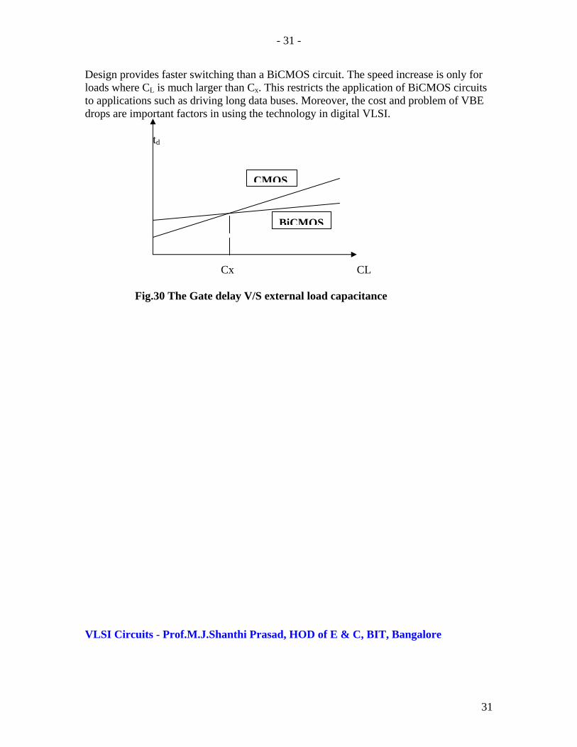
- 31 -
Design provides faster switching than a BiCMOS circuit. The speed increase is only for loads where CL is much larger than Cx. This restricts the application of BiCMOS circuits to applications such as driving long data buses. Moreover, the cost and problem of VBE drops are important factors in using the technology in digital VLSI. td
BiCMOS
CMOS
Cx CL
Fig.30 The Gate delay V/S external load capacitance VLSI Circuits - Prof.M.J.Shanthi Prasad, HOD of E & C, BIT, Bangalore
31

- 32 -
Solutions to problems in Design of High speed CMOS Logic circuits 8th chapter of John P.Uyemura:
8.1 Given Data: CL = 100 fF tro =123.75 ps CL = 115 fF tro =138.60 ps βn = βp, VTn = VTp
a) For a symmetric inverter,
( ) ( ) Ω=⎟⎟⎠
⎞⎜⎜⎝
⎛−
=⎟⎟⎠
⎞⎜⎜⎝
⎛−
= 1086.051.2
11
TnDDnn VV
Rβ
( ) ( ) Ω=⎟⎟⎠
⎞⎜⎜⎝
⎛−
=⎟⎟⎠
⎞⎜⎜⎝
⎛
−= 129
/7.0/58.11
//1
TpDDpp VV
Rβ
The formula for rise time tr = tro + αp CL for Cl = 100 fF, 123.75 = tro + αp x 100 (1) for Cl = 115 fF, 138.6 = tro + αp x 115 (2)
subtracting (2) from (1)
14.85 = 15αp ∴αp = 990
From Eqn. 7.71, As αp = 2.2 Rp
Rn = Rp = 990/2.2 = 450 Ω
Multiplying Eqn (1) by 100 and eqn (2) by 115 and by solving we get,
tro = 24.75 ps
From Eqn. 7.70, As tr0 = 2.2 Rp CFET , ∴CFET = 24.75/2.2 x 450 = 25 fF b) The general Expression for rise/fall time is ts = tr = tf = to + α CL
Substituting the calculated values, ts = tr = 24.75 ps + 990 x CL
c) As the width of transistors are increased by scaling the size by 3.2 times, the switching time equations for the new inverter becomes
ts = tr = tf = to + (α/S) CL
with α = 990, ts = tr = tf = to + 309.375 CL
with CL = 50 fF, ts = tr = tf = to + (α/S) CL = 24.75 + 309.375 x 50 = 40.218 ps with CL = 140 fF, ts = tr = tf = to + (α/S) CL = 24.75 + 309.375 x 140 = 68.062 ps [NOTE: to does not change, as the product Rp x CFET remains same].
32

- 33 -
VLSI Circuits - Prof.M.J.Shanthi Prasad, HOD of E & C, BIT, Bangalore 8.2 a) The calculated values of tr and tf for different values of CL are
CL tr tf 0 430 300
50 614 428 100 798 556 150 982 684 200 1166 812
The graph of tr V/S CL and tf V/S CL are as shown.
Rise Time V/S Load Capacitance
0
500
1000
1500
1 2 3 4 5
Load Capacitance
Ris
e Ti
me
Fall Time V/S Load Capacitance
0200400600800
1000
1 2 3 4 5
Load Capacitance
Fall
Tim
e
b)
1 1 0 1 0 Fig.31 Circuit of problem 8.2
1 2
0
CL
1 21 2
0
CL
0
CL
33

- 34 -
VLSI Circuits - Prof.M.J.Shanthi Prasad, HOD of E & C, BIT, Bangalore Three-inverter cascade is built using identical inverters. If the input to first stage of inverter is assumed to rise from low to high, the output of first stage falls from high to low. So, the switching equation of tf applies. As shown in fig.16, the switching equation of tr and tf applies to the second and third stage outputs.
tNOT/m=1 = tfo + αnu 2CL
tNOT/m=2 = tro + αpu 3CL
tNOT/m=3 = tfo + αnu 4CL
The total time delay is the sum of all the above individual gate delays. td = 2tf0 + tr0 + αnu 6CL + αpu 3CL
From the given equations, tf0 = 300, tr0 = 430, αnu = 2.56, αpu = 3.68, CL = 45 fF td = 2 x 300 + 430 + 2.56 x 6 x 45 + 3.68 x 3 x 45 = 265.1 ps
8.3 As the input to first stage of inverter rises from high to low, the output of first stage falls from low to high. So, the switching equation of tr applies. As shown in fig.32, the switching equation of tf, tr and tf applies to the second, third and fourth stage outputs.
1 2
m = 1A1
23
0
m = 2
1 2
m = 22
31
m = 1
m = 31 2
10 Cmin
Fig.32 Circuit of problem 8.3
tNOT/m=1 = tr0 + αpu 2Cmin
tNOR2/m=1 = 3tro + ⎟⎟⎠
⎞⎜⎜⎝
⎛2puα
2Cmin
tNAND2/m=2 =3tfo +2 αnu 3Cmin tNOT/m=3 = tr0 + αpu 4Cmin
The total time delay is the sum of all the above individual gate delays. td = 3tf0 +5tr0 +8αnuCmin + 5αpuCmin
VLSI Circuits - Prof.M.J.Shanthi Prasad, HOD of E & C, BIT, Bangalore
34

- 35 -
8.4 Given Data: Cox = 8 fF/μm2
r = 2.6 L = 0.4 μm VTn = /VTp/ Wn = 2.2 μm CL = 35 fF a) For Idealized Scaling, the expression for input Capacitance as given by equation 8.51 is Cin = (1 + r) CGn, where CGn = Cox AGn = CoxLWn ∴Cin = (1 + r)CoxLWn = (1 + 2.6) x 8 x 0.4 x 2.2 = 25.344 fF
b) For Idealized scaling, S = e = 2.71
( ) ⎟⎟⎠
⎞⎜⎜⎝
⎛=
⎟⎟⎠
⎞⎜⎜⎝
⎛
=1
1 lnln
ln
CC
SCC
N L
L
=
knowing the value of C1, the number of stages needed in the chain can be found out.
c) 111
ln CRCCeNS L
rd ⎟⎟⎠
⎞⎜⎜⎝
⎛== ττ
To calculate the delay time in the chain, information about C1 and R1 is needed.
8.5 As N = ⎟⎟⎠
⎞⎜⎜⎝
⎛
1
lnCCL = 768.6
10501040ln 15
12
≈=⎟⎟⎠
⎞⎜⎜⎝
⎛−
−
xx
The number of stages = 7
( ) 6.2800 71
1
1
==⎟⎟⎠
⎞⎜⎜⎝
⎛=
NL
CCS
The relative sizes are decided by the values of their β values β2 = (2.6)β1
β3 = (2.6)2β1 = 7 β1 β4 = (2.6)3β1 = 17 β1
β5 = (2.6)4β1 = 45 β1
β6 = (2.6)5β1 = 1167 β1
β7 = (2.6)6β1 = 302 β1 where we have rounded to the nearest integer.
VLSI Circuits - Prof.M.J.Shanthi Prasad, HOD of E & C, BIT, Bangalore
35

- 36 -
8.6 CL = 0.86 pF/cm,
Cin = 52 fF βn = βp r = 2.8 It is to design a driver chain such that, the output is a non-inverting one.
8.7 Equation 8.93 is ( )[ ]r
xSSττ
=−1ln and for rx ττ 72.0= , the eqn. Become
( )[ ] 72.01ln =−SS . This is a transcendental equation. This has a solution of S = 3.32. The following tabular column lists the values of the value of S for different
ratios of r
x
ττ
Sl.no.
r
x
ττ
Solution S
1 0.2 2.91 2 0.5 3.18 3 0.72 3.32 4 1 3.59
i.e. C2 = 8.8
C = 0.1 CL
r = 2.5
U4A
7405
1 2
U5A
7410
1122
13
U3A
7402
2
31
U2A
7400
1
23
CL
C1 C C3 C4
Fig.33 Circuit of problem 8.7
Path logical effort as per equn.8.135 is NOTNORNANDNAND ggggG 223=
Substituting the values of g for all the gates from eqns 8.130, 8.131 & 8.103, we get
46.315.3
65.35.4
5.35.51
121
12
13
==++
++
++
= xxxxrrx
rrx
rrG
The path electrical effort is 101.01
===CL
CLCCLH
The path effort is F = GH = 3.46 x 10 =34.6
The optimum stage effort is ( ) 43.26.34 411^=== NFf
VLSI Circuits - Prof.M.J.Shanthi Prasad, HOD of E & C, BIT, Bangalore
36

- 37 -
The total path delay as per eqn. 8.142 is ( ) PD += 43.24 Where P is the parasitic delay. As per eqn. 8.143, NOTNORNANDNAND PPPPP 223= and P of each gate is determined by the process specifications. The details about sizing are obtained by optimized quantities.
Starting from NAND3 gate, the electrical effort as per eqn.8.141 is
54.15714.1
43.2, 1
^
=== hgfhi
i
But as per eqn.8.116, the electrical effort is i
ii C
Ch 1+= , i = 1 to N
LCC
CCh
1.02
1
21 ==∴ , so that, C2 = 0.154CL
This NAND3 gate can be scaled by using eqn.8.125 as i.e. C1 = S15.5CGn ( rCSC Gnin += 31 )The remaining gates are analyzed in the same manner.
As gNAND2 = 1.2857, 8929.12857.1
43.2, 2
^
=== hgfhi
i
LCC
CC
h154.0
3
2
32 ==∴ , so that, C3 = 0.291CL
This NAND2 gate can be scaled by using eqn.8.125 as i.e. C2 = S24.5CGn ( rCSC Gnin += 22 )
As gNOR2 = 1.71, 421.171.143.2, 3
^
=== hgfhi
i
LCC
CCh
291.04
3
43 ==∴ , so that, C4 = 0.413CL
This NOR2 gate can be scaled by using eqn.8.127 as i.e. C3 = S36CGn ( rCSC Gnin 213 += )
As gNOT = 1, 421.171.143.2, 4
^
=== hgfhi
i
L
LL
CC
CCh
413.044 ==∴ , so that, CL = CL as required
This NOT gate can be scaled by using eqn.8.127 as i.e. C4 = S4Cref refin CSC 4=
37

- 38 -
VLSI Circuits - Prof.M.J.Shanthi Prasad, HOD of E & C, BIT, Bangalore We choose reference as the NOT gate with S4 = 1, C4 = CGn.
The scaling factor of NOR2 gate is
⎟⎟⎠
⎞⎜⎜⎝
⎛===
Gn
L
Gn
L
Gn CC
CC
CC
S 485.06291.0
63
3
The scaling factor of NAND2 gate is
⎟⎟⎠
⎞⎜⎜⎝
⎛===
Gn
L
Gn
L
Gn CC
CC
CCS 342.0
5.4154.0
5.42
2
The scaling factor of NAND3 gate is
⎟⎟⎠
⎞⎜⎜⎝
⎛===
Gn
L
Gn
L
Gn CC
CC
CCS 018.0
5.51.0
5.51
1
From Eqn.6.115, CGn = Cox(WnL), For the desired value of CL, the scaling factors S1 , S2, S3 and S4 can be determined. With these values, the channel width of the FETs can be determined. [NOTE: The students have been advised to study the example 8.4] 8.10
C1 1122
13
2
31 10C17400
1
23 2
31
Fig.34Circuit of problem 8.10
When the logic gate drives two or more gates, the data path splits. The capacitance contributed by the off path should also be considered in to account. Once the branching effort B has been calculated, the path effort gets modified to F=GHB and the remaining calculations proceeds in the same manner as without branching.
Path logical effort as per equn.8.135 is 222 NORNANDNOR gggG =
Substituting the values of g for all the gates from eqns 8.130, 8.131 & 8.103, we get
78.371.129.171.15.3
65.35.4
5.36
121
12
121
===++
++
++
= xxxxrrx
rrx
rrG
VLSI Circuits - Prof.M.J.Shanthi Prasad, HOD of E & C, BIT, Bangalore
38

- 39 -
The branching effort as per eqn.8.180is ( ) ( ) ( )
( ) 222.25.4
102
25)2(32
2
32 ==++
=+
+++=
+==
rr
rrr
CCC
CCB
NAND
NANDNAND
path
T
The path electrical effort is 101110
1===
CC
CCLH
The path effort is F = GHB = 3.78 x 10x2.222 = 84
The optimum stage effort is ( ) 38.484 311^=== NFf
The total path delay as per eqn. 8.142 is PD += )38.4(3 Where P is the parasitic delay. As per eqn. 8.143, 222 NORNANDNOR PPPP = and P of each gate is determined by the process specifications. The details about sizing are obtained by optimized quantities.
Starting from input NOR2 gate, the electrical effort as per eqn.8.141 is
56.271.138.4, 3
^
=== hgfhi
i
But as per eqn.8.116, the electrical effort is i
ii C
Ch 1+= , i = 1 to N
3
43 56.2
CCh ==∴ , so that, C4 = 2.56C3, As C4 = 10C1, C3 = 3.9C1
This NOR2 gate can be scaled by using eqn.8.125 as i.e. C3 = S36CGn ( rCSC Gnin 213 += )The remaining gates are analyzed in the same manner.
As gNAND2 = 1.2857, 41.32857.1
38.4, 2
^
=== hgfhi
i
2
32 431.3
CC
h ==∴ , so that, C3 = 3.41C2 , As C3 = 3.9C1, C2 = 1.114C1
This NAND2 gate can be scaled by using eqn.8.125 as i.e. C2 = S24.5CGn ( rCSC Gnin += 22 )
As gNOR2 = 1.71, 56.271.138.4, 1
^
=== hgfhi
i
1
21 56.2
CCh ==∴ , so that, C2 = 2.56C1, As C2 = 1.114C1, as required
VLSI Circuits - Prof.M.J.Shanthi Prasad, HOD of E & C, BIT, Bangalore
39

- 40 -
This NOR2 gate can be scaled by using eqn.8.127 as i.e. C1 = S16CGn ( rCSC Gnin 211 += )
The scaling factor of input NOR2 gate is
⎟⎟⎠
⎞⎜⎜⎝
⎛===
Gn
L
Gn
L
Gn CC
CC
CCS 0167.0
61.0
61
1
The scaling factor of NAND2 gate is
⎟⎟⎠
⎞⎜⎜⎝
⎛===
Gn
L
Gn
L
Gn CC
CCx
CCS 0248.0
5.41.0114.1
5.42
2
The scaling factor of output NOR2 gate is
⎟⎟⎠
⎞⎜⎜⎝
⎛===
Gn
L
Gn
L
Gn CC
CCx
CC
S 0709.05.5
1.09.36
33
From Eqn.6.115, CGn = Cox(WnL), For the desired value of CL, the scaling factors S1 , S2 and S3 can be determined. With these values, the channel width of the FETs can be determined.
VLSI Circuits - Prof.M.J.Shanthi Prasad, HOD of E & C, BIT, Bangalore
40

Chapter1. An Overview of VLSI 1.1 Introduction 1.2 What is VLSI? 1.3 Complexity 1.4 Design 1.5 Basic concepts An Overview of VLSI This chapter deals with the basic concepts of VLSI and VLSI DESIGN. A few questions such as what is VLSI/VLSI DESIGN? Why is VLSI? so on and so forth. The chapter looks at the VLSI DESIGN flow and the various options of design that are available for a designer. 1.1 Introduction The expansion of VLSI is ‘Very-Large-Scale-Integration’. Here, the term ‘Integration’ refers to the complexity of the Integrated circuitry (IC). An IC is a well-packaged electronic circuit on a small piece of single crystal silicon measuring few mms by few mms, comprising active devices, passive devices and their interconnections. The technology of making ICs is known as ‘MICROELECTRONICS’. This is because the size of the devices will be in the range of micro, sub micrometers. The examples include basic gates to microprocessors, op-amps to consumer electronic ICs. There is so much evolution taken place in the field of Microelectronics, that the IC industry has the expertise of fabricating an IC successfully with more than 100 million MOS transistors as of today. ICs are classified keeping many parameters in mind. Based on the transistors count on the IC, ICs are classified as SSI, MSI, LSI and VLSI. The minimum number of transistors on a VLSI IC is in excess of 40,000. The concept of IC was conceived and demonstrated by JACK KILBY of TEXAS INSTRUMENTS at Dallas of USA in the year 1958.The silicon IC industry has not looked back since then. A lot of evolution has taken place in the industry and VLSI is the result of this. This technology has become the backbone of all the other industries. We will see every other field of science and technology getting benefit out of this. In fact the advancements that we see in other fields like IT, AUTOMOBILE or MEDICAL, are because of VLSI. This being such important discipline of engineering, there is so much interest to know more about this. This is the motivation for this course namely ‘VLSI CIRCUITS’. 1.2 What is VLSI? VLSI is ‘Very Large Scale Integration’. It is the process of designing, verifying, fabricating and testing of a VLSI IC or CHIP.A VLSI chip is an IC, which has transistors in excess of 40,000. MOS and MOS technology alone is used. The active devices used are CMOSFETs. The small piece of single crystal silicon that is used to build this IC is called a ‘DIE’. The size of this die could be 1.5cmsx1.5cms. This die is a part of a bigger circular silicon disc of diameter 30cms.This is called a ‘WAFR’. Using batch process,

where in 40 wafers are processed simultaneously, one can fabricate as many as 12,000 ICs in one fabrication cycle. Even if a low yield rate of 40% is considered you are liable to get as many as 5000 good ICs. These could be complex and versatile ICs. These could be a PENTIUM Microprocessor IC of INTEL, or a DSP processor of TI costing around Rs10,000. Thus you are likely to make Rs50 million (Rs5crore) out of one process flow. So there is lot of money in VLSI industry. The initial investment to set up a silicon fabrication unit (called ‘FAB’ in short and also called sometimes as silicon foundry) runs into a few $Billion. In INDIA, we have only one silicon foundry-SCL at Punjab (Semiconductor Complex Ltd., in Chandigarh). Very stringent and critical requirements of power supply, cleanliness of the environment and purity of water are the reasons as to why there are not many FABS in India. 1.3 Producing a VLSI chip is an extremely complex task. It has number of design and verification steps. Then the fabrication step follows. The complexity could be best explained by what is known as ‘VLSI design funnel’ as shown in the Figure1.1. Figure1.1 The VLSI design tunnel

CHAPTER 3.0
PHYSICAL STRUCTURE OF CMOS ICs 3.1 IC Layers 3.2 MOSFETs 3.3 CMOS Layers 3.4 Designing FET array 3.5 Summary References PHYSICAL STRUCTURE OF CMOS ICs
3 VLSI chip design flow as discussed in the chapter 1, has two parts namely, the front-end design and the back end design. The front-end design is all about logic and circuit design of the chip. The back end design translates the circuit elements – active, passive components and their interconnections to respective layouts. These are the layouts, which ultimately sit on the silicon die at different layer levels to get the finished IC. The actual dimensions of these innumerable polygons have to be designed. The optimal placing (helps in saving silicon real estate) and routing (helps in achieving required speed of operation) of these polygons is also part of the back end design. This is called the ‘ physical design’. This chapter discusses the various layers that one sees on an IC in general and looks at the details of a CMOS process. A number of example circuits have been dealt to show how the layouts are done optimally. This chapter will examine the physical structure of a CMOS IC as seen at the microscopic silicon level in the design hierarchy.
3.1 IC Layers Any IC in general will have some conducting, semi conducting and the insulating layers stacked vertically. These are starting semiconductor wafer, silicon dioxide (insulator), diffusion (or implant), polycrystalline silicon (gate material in- short-polysilicon) and the top metal layer. Using these layers, geometrical patterns are done and appropriate connectivity is established among all the physical patterns. The layout details of a basic IC is shown in Fig.3.1
(a) (b)
S D P-Substrate
Gate
SiO2 G SiO2 G A T E

Figure.3.1. IC layout (a) cross-sectional view (b) Top view Once the layout details are known it is to evaluate the resistance and capacitance values of the physical entities sitting on the silicon. This is required to evaluate the delay encountered by the signal in flowing from one component to an other. The sheet resistance (Rs) of each of the layers will be known in advance. Knowing the Rs value of a layer, one can calculate the resistance of the pattern made out of a particular layer. 3.1.1 Sheet resistance The resistance of layer with resistivity ρ and with the dimensions as shown in Fig.3.2 is given by
Rs = ρ L = ρ L/ W. t A 3.1
Where A = cross-sectional area of the layer, ρ = Resistivity of the layer material in ohm-cm, L = the length of the layer, W = the width of the layer, t = thickness of the layer. In equation 3.1 if W = L, Rs = ρ / t = Sheet resistance (ohms per square). Thus the sheet resistance of layer is defined as the resistance offered to the flow of current by the layer of thickness ‘t’ and a perfect square. If the given layer is not a perfect square, you can calculate equivalent number of squares ‘N’ (= L/W). Then the resistance R = N.Rs = Z.Rs. ‘Z’ (L/W) is a number and it is the reciprocal of the aspect ratio.
ρ t L I W Figure.3.1. The geometry of a layer 3.1.2 Layer capacitance Knowing the area of the layer and the dielectric constant, area capacitance can be calculated using the equation: C = ε A / t 3.2
Where ε = ε0 εins, and t = thickness of the layer ε0 = 8.854 x10 –14 F/cm, εSio2 = 4.0, A = Area of the layer 3.1.3 Delay timer constant The product of the resistance and the capacitance gives the delay time constant ‘τ’. The output of a gate passes to an input of a gate through a connecting wire, which has a

resistance of Rline. There will be a capacitance (gate capacitance) at the input of the gate as shown in the Fig 3.2. The signal will take ‘τ’ seconds to reach the input of the gate 2 from the output of the gate 1.
Gate1 Line Gate2 Rline Cin Cline
Figure.3.2 Delay through the interconnect wire between the 2 gates. 3.2 MOSFETs Whenever a polysilicon cuts across the diffusion, at the intersection a MOSFET is formed. In between these layers silicon dioxide is sand witched and you get the field effect. While writing the layout diagrams oxide layer will not be shown. Other layers like diffusion, polysilicon and the metal layer are shown. The NMOSFET symbol and its layout are shown in the Fig.3.3. Gate Gate Drain Source
(a) (b)
Figure.3.3 NMOSFET a) symbol, b) layout
3.2.1 Current Flow in a FET The current in a NMOSFET is due to flow of electrons from source to drain under the influence of applied drain voltage VDD. The device goes to on state with VGS ≥ VT. Here, VGS is the gate voltage with respect to the source, and VT is the threshold voltage of the enhancement NMOSFET under consideration. Threshold voltage is the gate voltage with respect to source at which the substrate underneath the gate between the source and the drain gets inverted and the N-channel is formed. Now with VDD on, the electrons move from source towards the drain. And the conventional drain current flows from drain to source. The magnitude of the current is proportional to the total charge created in the channel and inversely proportional to the transit time of the electrons. The schematic of the NMOSFET showing the current flow is depicted in the Fig.3.4. S G D VDD
τ = Rline. Cin
D S
sNn Channel P-Substrate
n+ n+
Key: Metal Poly silicon Diffusion Field oxide
Gate oxide

Figure.3.4 Schematic of NMOSFET with different layers The expression for IDS can be deduced as: I DS = Charge in the channel / Transit time of electrons = Q / τSD
Where τSD = Channel length / Electron drift velocity = L / μn EDS = L / μn VDS / L = L 2 / μn VDS 3.3 The channel charge is given by: Q = - C G (VGS – VT) 3.4 Where CG = Gate oxide Capacitance, as given by Equation 3.2 Combining Equations 3.3 and 3.4 we get, IDS = ε0 εox μn W/ (L t ox) . (VGS –VT) .VDS 3.5 = βn. (VGS – VT).VDS Where βn = gain factor (A/ V2) 3.3 CMOS Layers CMOS FETS are fabricated using three processes, namely i) N-Well process ii) P- Well process and iii) Twin –Tub Process. If the process is started with a P-substrate, NMOSFETs can be fabricated. On the same wafer, to put PMOSFET, one should have a N- semiconductor. This active N- area is obtained by ion implantation. This is called the N-Well. You should have a P-Well to accommodate NMOSFETs, if the starting material is a N-substrate. In the case of twin –tub process, an epitaxial layer of single crystal silicon is grown by chemical vapor deposition process (CVD). On this layer, both N-well and P-Well implants are done to accommodate PMOS and NMOS FETs. The top view of the patterning of the FETs in a N-Well process is shown in the Fig.3.5.For the implementation of a particular logic; the NMOSFETs and PMOSFETs may have to be connected in series or parallel.

n+ n+
P+ p+
N-Well
P+ p+ n+ n+
Figure.3.5 Top view of patterning of the FETs 3.4 Designing FET arrays When a logic gate is implemented, NMOSFETs are arranged in the pull-down structure. These transistors will depend upon the input pins of the gate. Depending on the Boolean expression, these transistors are connected in series, parallel or series-parallel combination. In any case these transistors could be arranged in an array. In order to optimize the silicon space, layout design of these arrays is a must. Same thing hold good for the PMOSFET arrays, which come as pull-up devices between VDD and the output line. We shall discuss the design of the FETs connected in series and parallel.
3.4.1 NMOSFETs in series/ parallel Silicon patterning for two NMOSFETs connected in series is shown in Fig.3.5. D1 S1 D2 S2 D1 S1 D2 S2 (a) (b) Figure.3.5 Silicon patterning of 2 NMOS FETs in series
Silicon patterning of the 2 NMOSFETs connected in parallel is shown in Fig.3.6. x A B y (a) (b) Figure.3.6 Patterning of the 2 NMOSFETs connected in parallel (a) Schematic (b) Layout 3.4.2 Layout of a NOT gate

The circuit schematic and the corresponding layout is shown in the Fig.3.7.In the NOT gate NMOSFET is connected in series with the PMOSFET. The drains of the 2 transistors are connected to the metal wire, which goes out as an output line. Similarly the two gates of polysilicon have been connected together and the intersection points goes to the output line. VDD VDD x x x y VSS VSS
(a) (b) Figure.3.7 Circuit to layout translation of NOT gate The basic procedure to adopt while drawing layout diagrams for any logic circuit is to make the circuit of the logic circuit. Then identify the drain and source of the NMOS and the PMOS transistors. The source of PMOS will be connected to VDD and the source of the NMOS will be connected to VSS. The drain(s) of bottom most transistor(s) is (are) connected to the drain (s) of the top most transistor(s). This junction is the output line. The polysilicon layer cuts across the P-diffusion and the N- diffusion to form the two transistors and the junction is the input line. Following the above given procedure layout of any logic gate can be easily drawn. 3.5 Summary The various layers, which make an integrated circuit, are identified in this chapter. The layers that are stacked together for simple CMOS process are explained. The logic circuits can be easily translated to the layouts by following standard procedure. The different layers are drawn in different colours. But a state of art of VLSI chip will have many more layers. There could be 6-10 metal layers. When all these layers are stacked on top of an other, you get a fat IC. The layout details of a transistor and the circuit will give you a correct picture of the process flow. The order in which the layers are integrated on the substrate will be clear. REFERENCES(for all the 3 chapters) 1.Introduction to VLSI circuits and systems: John P. Uyemura, Edition 2005, John Wiley & Sons, Inc. 2.Basic VLSI design: D.A. Pucknell, K.Eshraghian, III Edition, Prentice-Hall OF India Pvt.Ltd. 3.CMOS Digital Integrated Circuits –Analysis and Design: Sung- Mo Kang, Yusuf Leblebici, III Edition.,Tata McGraw-Hill Publishing Company LTD., 4. Application –specific Integrated Circuits: Smith, Addison Wesley 1997.

5. CMOS Circuit design, Layout and Simulation: R.Jacob Baker, IEEE Press.,2000 6. Principle of CMOS VLSI Design: Neil Weste and K. Eshraghian Addison Wesley.,1998.

ELEMENTS OF PHYSICAL DESIGN 3.1 Introduction to Physical Design Several equivalent viewpoints may be used to describe an integrated circuit. To a circuit designer, a chip is the physical realization of an electronic network. A logic designer, on the other hand, may choose to view the chip as a device that performs functions specified by logic diagrams, function tables, or an HDL file. Figure 3.1 illustrates how different people might view the same thing. Regardless of the abstraction used, in the final analysis, an integrated circuit is really an intricate physical object that has been carefully designed and fabricated. Physical design in VLSI deals with the procedure needed to realize a circuit on the surface of a semiconductor wafer. Starting with the electrical network schematic, computer tools are used to create the necessary patterns on each layer in the 3-dimensional structure. Once the drawings are completed, the information can be used to fabricate the masks needed in the processing line. CMOS technology allows one to choose from a wide variety of circuit design techniques, any of which may be useful when implementing a given logic function. This feature is particularly nice when designing high-performance circuits, as often one design style yields faster switching than another. Physical design is critical in this situation, since the layout and the resulting performance are directly linked to each other. At this level, the circuit design and layout are indistinguishable. Many people view physical design as a skill that is best learned by doing. The most proficient designers tend to be the most experienced, but, of course, one must begin somewhere. In this chapter, we will introduce the first ideas of physical design by examining the concept of layout in more detail. This includes ideas such as design rules and interconnect routing. The details of designing CMOS circuits will be covered in the following chapters. 3.2 Masks and Layout Drawings Every material layer in an integrated circuit is described by a set of geometrical objects of specified shape and size. These objects are defined with respect to each other on the same layer, and also with reference to geometrical objects that lie on other layers, both above and below. Layout drawings relay this information graphically, and can be used to generate the masks needed in the fabrication process. Because of this relationship, we will take the viewpoint that a layout drawing represents the top view of the chip itself. When we visualize an integrated circuit, it appears as a set of overlapping geometrical objects. In a layout editor, each layer is described by using a distinct color or fill pattern that allows us to see the objects relative to each other. Once we get oriented to seeing an integrated circuit in this manner, it is a simple matter to construct transistors and route the interconnect lines as required. While classical schematic representations provide the topology of the network, the layout gives us the
Prof.Hansaraj Guhilot, KLE, Belagaum

ability to modify the performance of a circuit. Performing the layout is therefore an intrinsic part of the design process. When designing digital logic circuits in CMOS, the goals remain quite simple: • Design a circuit that implements the logic function correctly, and, • Adjust the parameters to meet the electrical specifications. This is often more difficult than it sounds, particularly when we note that state-ofthe art VLSI chips can have several million MOSFETs with the associated interconnect lines. At the most basic level, we find that many problems arise when performing the layout of an integrated circuit. Some deal with the practical aspects of circuit operation, others originate from physical properties of the materials involved, and yet others are due to limitations in the fabrication processes. These all contribute to the techniques used in the physical design. 3.3 Design Rule Basics Design rules are a set of guidelines that specify the minimum dimensions and spacings allowed in a layout drawing. They are derived from constraints imposed by the processing and other physical considerations. Violating a design rule may result in a non-functional circuit , so that they are crucially important to enhancing the die yield. Limitations in the photolithography and pattern definition give rise to several critical design rules. Since these are strongly dependent on equipment used in the fabrication process, they tend to change with improving technology. The situation is complicated by the fact that physical phenomena and device design considerations also enter into the picture. In this section, we will examine some of the
design rules associated with a CMOS processing technology. . 3.3.1 Minimum Linewidths and Spacings Consider the two objects shown in Figure 3.2. These represent two patterns on the same layer, e.g., both are polysilicon. When used as interconnects, the two rectangles shown in the drawing are called "lines" (since every physical patterning must have a non-zero width), and we will use this terminology in our discussion. The minimum linewidth X is the smallest dimension permitted for any object in the layout drawing; X is also known as the minimum feature size. The minimum spacing S is the smallest distance permitted between the edges of two objects; in the present example, the minimum spacing is between the two lines. Minimum linewidth and spacing values for interconnect lines may originate from the resolution of the optical printing system, the etching process, or from other considerations such as surface roughness. Violating the minimum linewidth rule may result in ill-defined or broken interconnects. Similarly, the minimum spacing rule ensures that the lines are physically separated in the final structure. If this
Prof.Hansaraj Guhilot, KLE, Belagaum

guideline is not followed, then the two may form an electrical short in the circuit. The situation is more complicated when applied to patterning a doped region in the silicon because of lateral doping effects and the presence of depletion regions. Lateral doping is shown in Figure 3.3. In (a), the oxide has been patterned by the lithography to have a linewidth X. However, when the wafer is heated to anneal the implant, lateral diffusion2 increases the actual width of the n+ region to X'>X. This Note that even a single defect results in a non-functioning circuit.
effect is important when determining the minimum spacing 5 between adjacent doped lines. Depletion effects also influence the value of 5. As shown in Figure 3.4, a depletion region exists at every pn junction. Let us assume for simplicity that the junction has a step-doping profile where the impurity concentration changes abruptly from Nd on the n-side to Na on the p-side. With a reverse-bias voltage of VK, the total depletion width xd can be computed from
is the zero-bias value of the total depletion width, and (3-3) is the built-in voltage. Table 3.1 provides a list of useful numerical values for basic calculations. Note that the intrinsic concentration ni applies only to silicon at room temperature (T=300° K). To calculate the p-side depletion width xp shown in the drawing, we use
Since this increases with the reverse bias voltage, the minimum spacing distance 5 often accounts for the worst-case situation, i.e., when VR=VDD. From this discussion, it is not surprising that the minimum width and spacing for n+ and p+ regions are usually larger than those for a polysilicon line. 3.3.2 Contacts and Vias Contacts and vias are used to provide electrical connections between different material layers. In general, contacts are necessary connections to access the various regions of silicon, while vias are used between two interconnect layers to simplify the layout. When formulating design rules for these types of objects, two important considerations arise: the physical size of the oxide cuts, and the spacing needed around the connection on the layers.
Prof.Hansaraj Guhilot, KLE, Belagaum

Let us first examine the dimensions of a contact region. The geometry is shown in Figure 3.5. It is apparent that the minimum size is limited by the lithographic process. However, this does not imply that one uses the largest contacts possible, as other considerations come into play. If the contact cut is too large, then it may be difficult to attain complete coverage when depositing the upper layer. Large contact cuts may result in cracks or voids, that may in turn lead to a circuit failure. To overcome this problem, it is common to restrict the dimensions of contact cuts to prespecified values that can be reliably made in the fabrication process. Now, consider the problem of spacing x around an oxide cut as shown in Figure 3.6. We must specify the minimum distance between the edge of an oxide cut and the edge of a patterned region to allow for misalignment tolerances in the masking steps. These are generically classified as registration errors, and arise because it is not possible to align the mask with arbitrary precision.
3.3.3 MOSFET Rules MOSFETs are usually fabricated using the self-aligned technique described in the last chapter. This approach uses the polysilicon gate as a mask for the ion implantation step that forms the drain/source regions. Certain precautions must be taken in the physical design to ensure that small registration errors can be tolerated, and functional transistors will still be formed. First, we recall that n+ regions in an nFET are described by the derived layer1
ndiff = (ACTIVE) AND (NSELECT). With regard to the fabrication sequence, this means that an n+ region is formed where (a) the NSELECT mask gives an opening in the photoresist, AND, (b) an ACTIVE area exists to allow the implant to penetrate into the silicon substrate. Since the formation of the physical ndiff layer relies on the overlap of two masks, the size of the NSELECT region must be larger than the size of the corresponding ACTIVE area. The drawing in Figure 3.7(a) shows the proper sizing of the two layers, with the NSELECT rectangle larger than the ACTIVE area rectangle. The final dimensions of the n+ region are those of the ACTIVE area. A minimum spacing value x between the edges of the two masks is used to allow for registration error between
Prof.Hansaraj Guhilot, KLE, Belagaum

the two masks. Even though the ion implant specified by the NSELECT boundary is larger than needed, the thick field oxide specified by the region NOT( ACTIVE) prevents the underlying silicon from being doped. This is verified by the cross-sectional view shown. If we reverse the situation and make the ACTIVE area larger than the NSELECT area, then only the region described by ndiff=(ACTIVE) AND (NSELECT) will become n+; sections corresponding to (ACTIVE) AND [NOT(NSELECT)] remain p-type substrate. This is shown in Figure 3.7(b). The ndiff region does not have the correct cross-sectional pattern needed to ensure proper isolation and operation. Consider next the gate overhang distance d shown in Figure 3.8. This is included to ensure that a misaligned gate will still yield a structure that has separate drain and source regions. To understand the reasoning, suppose that a MOSFET is designed using the layout shown in Figure 3.9(a) with d=0. Figure 3.9(b) shows a
small misalignment where the polysilicon does not traverse the entire active area. Since the ion implant will dope all of the exposed substrate, the resulting structure shown in (c) has the drain and source n+ regions merged into one. Electrically, the drain and source are shorted, so the device cannot control the current flow, i.e., the switching action has been lost. The same consideration applies to a MOSFET where the n+ region changes shape as shown in Figure 3.10. The channel width W is a critical design parameter, so that the spacing s between the poly and n+-edges must be large enough to ensure that the MOSFET still has the proper value if small registration errors occur. 3.3.4 Bloats and Shrinks The drawings produced by a layout editor provide the basic view of an integrated
Prof.Hansaraj Guhilot, KLE, Belagaum

circuit that are used to extract the equivalent device parameters. It is therefore important to understand the correlation between what is shown on the computer monitor when compared with the actual die after fabrication. In general, the final size of a physical layer will be different from the dimensions specified by the mask that created the pattern. Two obvious examples are • ACTIVE: Encroachment reduces the size of the usable active area. • Doped n+ or p+: Lateral doping effects increase the size of these regions. In addition, the physical process of etching a material layer is anisotropic, with both vertical and lateral etching present. Although the lateral etch rate can be reduced
using various techniques, it cannot in general be reduced to zero. The effect of anisotropic etching on a polysilicon layer is illustrated in Figure 3.11. The question that naturally arises at this point is "What does the layout drawing represent relative to the finished chip?" In other words, will the chip patterns be identical to those shown by the layout editor, or are size adjustments necessary? In the early days of chip design, one had to increase or decrease the size of the layout drawing to view the actual chip dimensions. However, it is now common for the chip fabricator to subject the masks to bloats (increases in object sizes) and shrinks (decreases in the object size) as needed to compensate for the difference between the mask dimensions and the resulting size on the chip. When this is done, then the layout editor displays a reasonably accurate view of the finished circuit. These considerations are particularly important to designing a MOSFET. Although the two critical dimensions L (the channel length) and W (the channel width) are related to the drawn mask values, the values are different as shown in Figure 3.12. The channel length L that is required in the current flow equations is reduced from the drawn value L' by L = L - 2L (3.5) where L0 is the overlap distance from lateral diffusion effects . In a similar manner, the channel width W is smaller than the drawn ACTIVE width W because of active area encroachment. This is where the usable size of the active area is reduced because of oxide growth underneath the edges of the nitride pattern. If the encroachment per side is (AW), then W = W-2(ΔW) (3.6) gives the proper electrical value. This can become confusing when entering the device dimension into a circuit simulation program. For example, SPICE parameters can be entered using either the drawn or physical values so long as the remaining data values are consistent. This will be discussed in more detail in the next chapter. The gate overlap L0 is also known as the lateral diffusion length LD.
Prof.Hansaraj Guhilot, KLE, Belagaum

3.4 Types of Design Rules Geometrical design rules are a set of minimum widths, spacings, and layout guidelines needed to create the masks. There are two ways to specify these dimensions: • Specific Values: All dimensions are stated in standard unit of length, such as the micron; • Scalable: Distances are specified as multiples of a metric λ, that has dimensions of length. The actual value of λ, is adjusted to correspond to the limitations of the process line. Both approaches are common in CMOS VLSI. Scalable rules have the advantage that they can be adjusted to several different processing lines by changing the value of λ. However, this does not come without cost. Since every distance is specified as a multiple of λ, the numerical value is dictated by the worst-case situation. This generally decreases the compaction density of the circuit compared to what is attainable if the parameters are specified in an absolute metric such as microns. In general, there are three main classes of design rule specifications. These are • Minimum Width, • Minimum Spacing, and, • Surround. Surround rules apply to objects placed within larger objects (such as contacts). Every layer has a minimum width and minimum spacing value, while surrounds are specified as required.
3.5 CMOS Design Rules In this section, we will examine a basic set of CMOS design rules to understand the presentation and meaning of each type of rule. This set has been provided in the setup technology file as ledit.tdb, and is also available with the name morbn20.tdb. The DR set describes the MOSIS Orbit 2-micron double-poly, double- metal, n-well CMOS process; the technology name for this process is SCNA (for Scalable CMOS N-Well Analog). For the purposes of this discussion, we will not list all layers. In particular, the POLY2 layer is not shown explicitly here to simplify the discussion. A complete design rule set contains all of the geometric limits for mask layout. This includes the minimum feature sizes and minimum spacings on each mask, and also provides layer-to-layer spacings when necessary. In order to list the rules in an easy-to-find format, they are presented according to the order of the masks used in the processing. The primary design rule layers for the morbn20 technology are listed in Table 3.2.
Prof.Hansaraj Guhilot, KLE, Belagaum
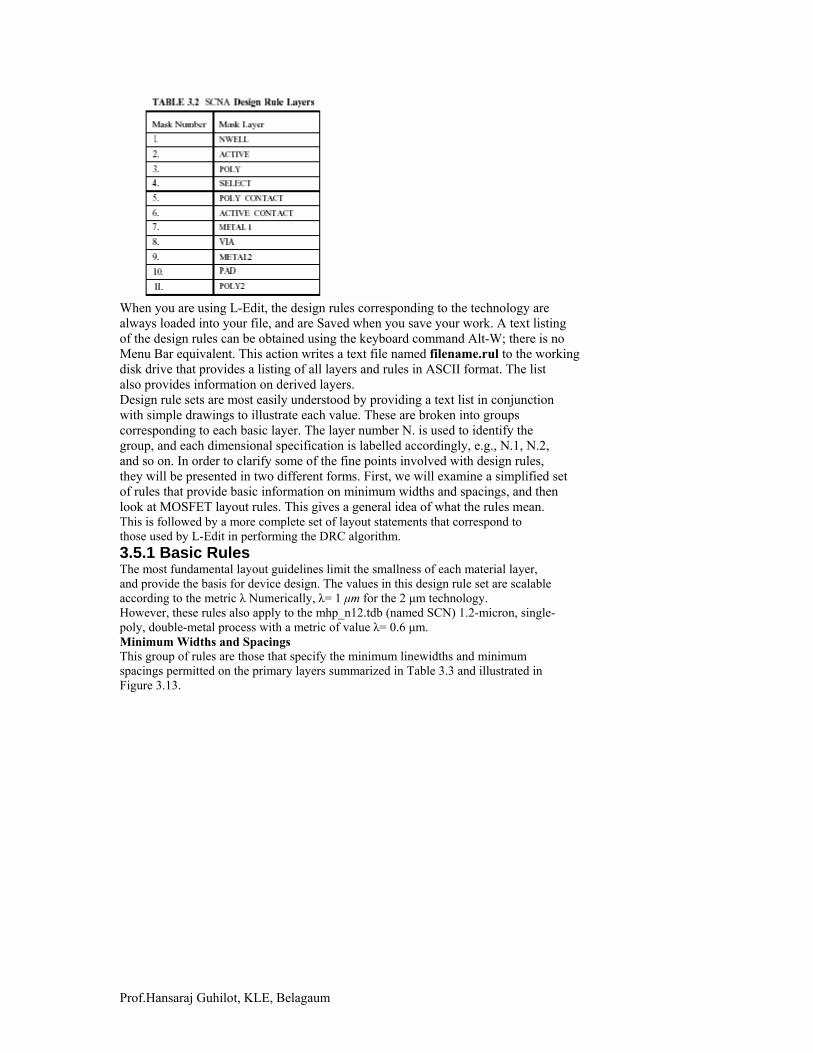
When you are using L-Edit, the design rules corresponding to the technology are always loaded into your file, and are Saved when you save your work. A text listing of the design rules can be obtained using the keyboard command Alt-W; there is no Menu Bar equivalent. This action writes a text file named filename.rul to the working disk drive that provides a listing of all layers and rules in ASCII format. The list also provides information on derived layers. Design rule sets are most easily understood by providing a text list in conjunction with simple drawings to illustrate each value. These are broken into groups corresponding to each basic layer. The layer number N. is used to identify the group, and each dimensional specification is labelled accordingly, e.g., N.1, N.2, and so on. In order to clarify some of the fine points involved with design rules, they will be presented in two different forms. First, we will examine a simplified set of rules that provide basic information on minimum widths and spacings, and then look at MOSFET layout rules. This gives a general idea of what the rules mean. This is followed by a more complete set of layout statements that correspond to those used by L-Edit in performing the DRC algorithm. 3.5.1 Basic Rules The most fundamental layout guidelines limit the smallness of each material layer, and provide the basis for device design. The values in this design rule set are scalable according to the metric λ Numerically, λ= 1 μm for the 2 μm technology. However, these rules also apply to the mhp_n12.tdb (named SCN) 1.2-micron, single- poly, double-metal process with a metric of value λ= 0.6 μm. Minimum Widths and Spacings This group of rules are those that specify the minimum linewidths and minimum spacings permitted on the primary layers summarized in Table 3.3 and illustrated in Figure 3.13.
Prof.Hansaraj Guhilot, KLE, Belagaum

MOSFET Layout The basic layout rules for MOSFETs are illustrated in Figure 3.14, and the values are summarized in Table 3.4. Dimensions that deal with POLY and N+/P+ apply equally to both nFETs and pFETs. Contacts (cuts in the oxide that allow electrical connections between two layers) to N+/P+ are called ACTIVE CONTACTS, while POLY CONTACTS provide access to the POLY layer (which must be in field regions). In this technology, p-channel MOSFETs must be inside n-well regions, and sufficient spacing must be provided between opposite-polarity regions (i.e., between n+
and p+ sections) as well as between P+ regions and the NWELL edge. Spacing requirements also apply between different n-well regions; in general, a larger space is needed if the n-wells are biased at different voltages, due to the voltage dependence of depletion regions.
3.5.2 Mask-Based Design Rule Set At the layout level, design rules apply to the masks involved in the chip patterning process. L-Edit employs a complete set of rules that apply to both masking layers and derived layers. Using derived layers allows us to make the connection between the individual patterns and the material layers that are important to the operation of transistors and other devices. Figures 3.15, 3.16, and 3.17 provide most of the SCNA design rule set using
Prof.Hansaraj Guhilot, KLE, Belagaum
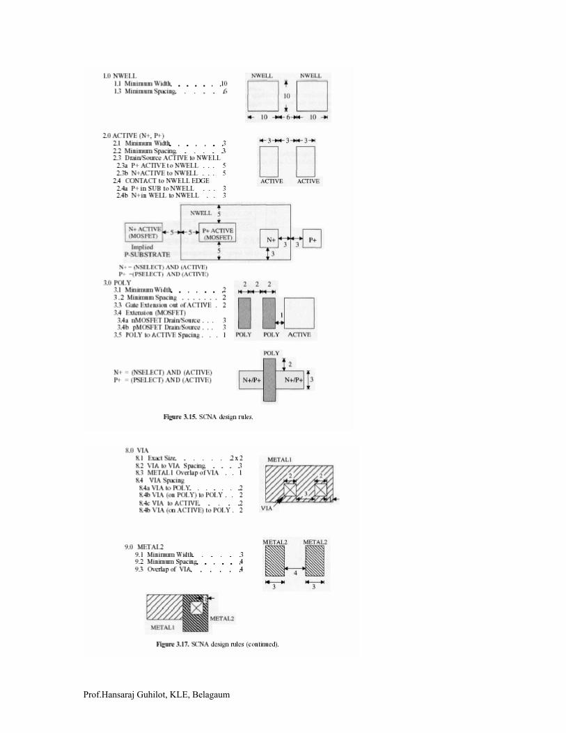
Prof.Hansaraj Guhilot, KLE, Belagaum

values in conjunction with drawings. Some have been omitted or merged for simplicity, but can be accessed by having L-Edit print the complete set. In the drawings, note that the derived layers N+ = (NSELECT) AND (ACTIVE) P+ = (PSELECT) AND (ACTIVE) are equivalent to ndiff (n+) and pdiff (p+) doped regions. 3.8 Latch-Up Latch-up is a condition that may occur in CMOS integrated circuits where • The circuits cease to operate; • There is excessive consumption of current from the power supply, which may cause overheating and chip failure; and, • The only way to take the chip out of latch-up is to disconnect the power supply. Latch-up originates from the n and p layers used to create nMOS and pMOS transistors in the CMOS fabrication process. As such, it can be prevented by following certain rules in the layout and electrical connections. Let us first examine why latch-up occurs. Figure 3.28 shows a basic cross-section of an n-well CMOS chip. Note that the power supply and ground connections have been included. Following the connections from VDD to ground shows the existence of a 4-layer pnpn structure: p+ connected to VDD; n-well; p-substrate; n+ connected to ground. If the chip goes into latch-up, current flows from the power supply to ground as shown. The circuits do not function since they do not receive any current. In power electronics, the pnpn layering scheme is used to create a device known as a silicon-controlled rectifier (SCR), which is used as a switched rectifier.The I- characteristics are shown in Figure 3.29. For small voltages, the structure acts like a reverse-biased pn junction, and only leakage current flows. However, if the applied voltage reaches the break-over voltage VBO, then the curve exhibits a negative slope. This results in a very quick drop in the voltage accompanied by an increase
in the current. In CMOS, this corresponds to the chip going into latch-up. Latch-up is often explained using bipolar transistor models. The drawing shows that both pnp and npn transistors can be visualized from the layering. Since the two
Prof.Hansaraj Guhilot, KLE, Belagaum

transistors share the internal n and p layers, they are automatically connected in a feedback loop. Using this viewpoint, latch-up occurs when the sum of the commonbase current gains equals unity:
One approach to reducing the occurrence of latchup is to ensure that the gains of the bipolar transistors are kept small by reducing the efficiency of the emitter and base regions. At the physical design level, latch-up prevention is achieved by adhering to a set of rules that are designed to either distribute the voltages throughout the layered regions, or reduce the current gain of the bipolar transistors. The following items are common to most processes. • Use guard rings around MOSFETs; • Provide liberal substrate contacts to ground, and n-well contacts to VDD; • Obey all design rules. Guard rings are p+ regions connected to ground surrounding nMOSFETs, or n+
regions connected to VDD surrounding pMOSFETs, that are added to reduce the gains of the parasitic bipolar transistors. Latch-up prevention techniques are usually specified for a given fabrication process, and should be followed to ensure a functional design.
Prof.Hansaraj Guhilot, KLE, Belagaum

Prof.Hansaraj Guhilot, KLE, Belagaum

Prof.Hansaraj Guhilot, KLE, Belagaum

Prof.Hansaraj Guhilot, KLE, Belagaum

Prof.Hansaraj Guhilot, KLE, Belagaum

Prof.Hansaraj Guhilot, KLE, Belagaum

Prof.Hansaraj Guhilot, KLE, Belagaum

Prof.Hansaraj Guhilot, KLE, Belagaum
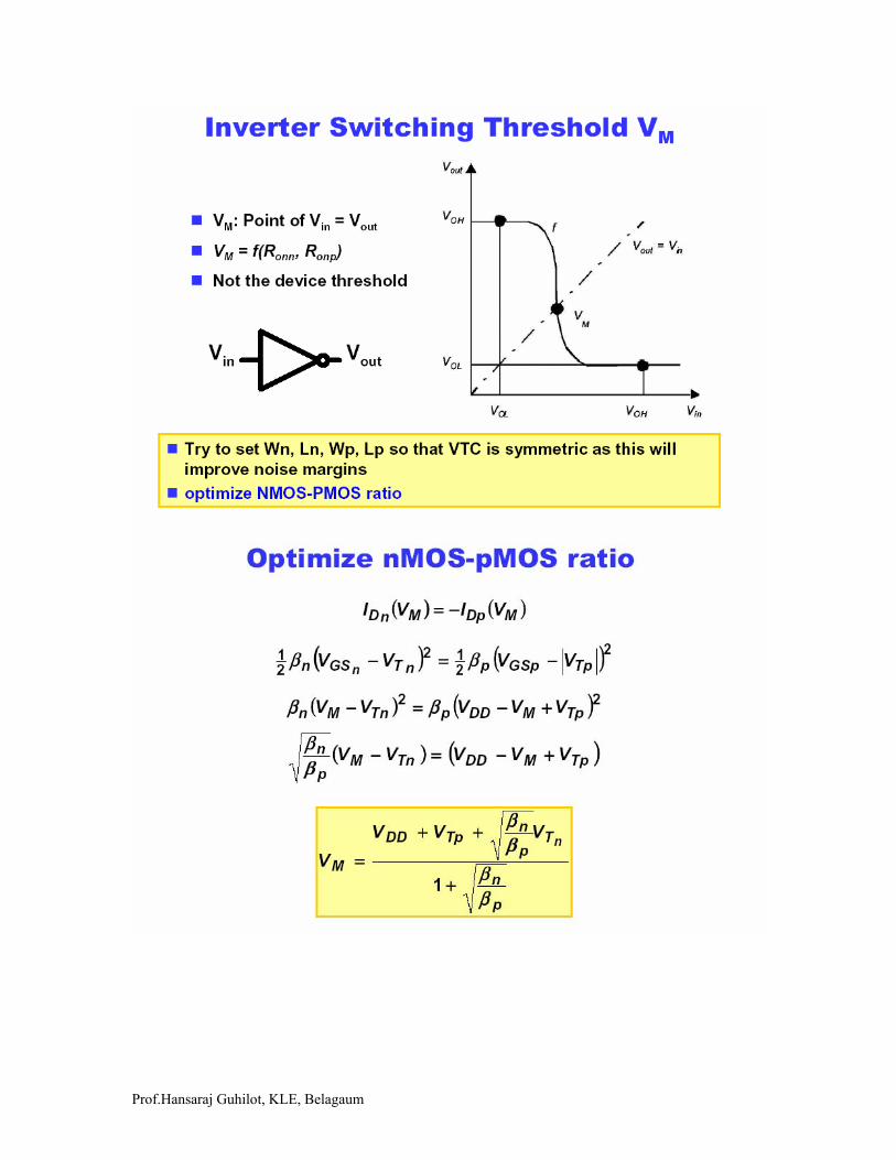
Prof.Hansaraj Guhilot, KLE, Belagaum
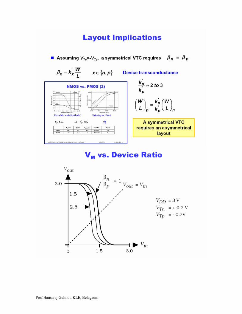
Prof.Hansaraj Guhilot, KLE, Belagaum

Prof.Hansaraj Guhilot, KLE, Belagaum

Prof.Hansaraj Guhilot, KLE, Belagaum

Prof.Hansaraj Guhilot, KLE, Belagaum

Prof.Hansaraj Guhilot, KLE, Belagaum
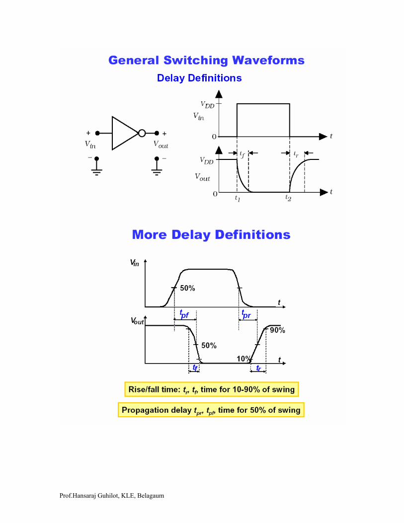
Prof.Hansaraj Guhilot, KLE, Belagaum
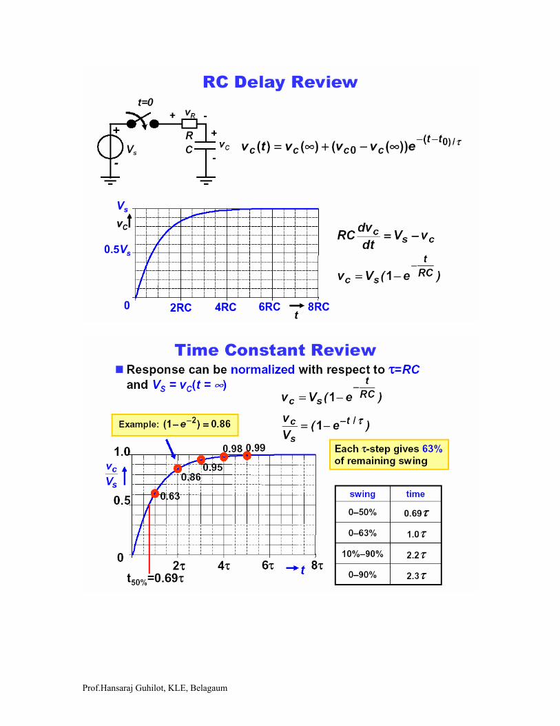
Prof.Hansaraj Guhilot, KLE, Belagaum

Prof.Hansaraj Guhilot, KLE, Belagaum

Prof.Hansaraj Guhilot, KLE, Belagaum
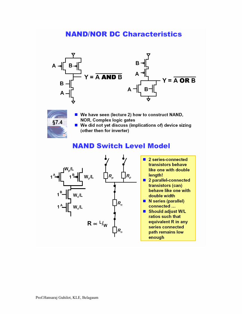
Prof.Hansaraj Guhilot, KLE, Belagaum

Prof.Hansaraj Guhilot, KLE, Belagaum

Prof.Hansaraj Guhilot, KLE, Belagaum
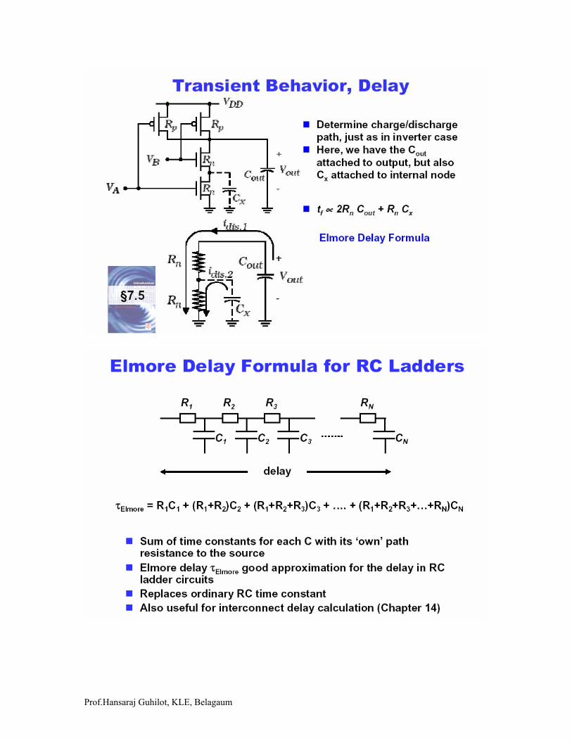
Prof.Hansaraj Guhilot, KLE, Belagaum
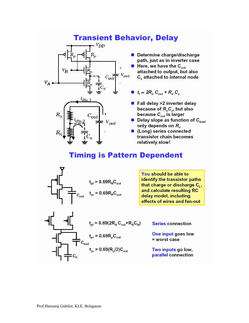
Prof.Hansaraj Guhilot, KLE, Belagaum

Prof.Hansaraj Guhilot, KLE, Belagaum

Prof.Hansaraj Guhilot, KLE, Belagaum
Prof.Hansaraj Guhilot, KLE, Belagaum
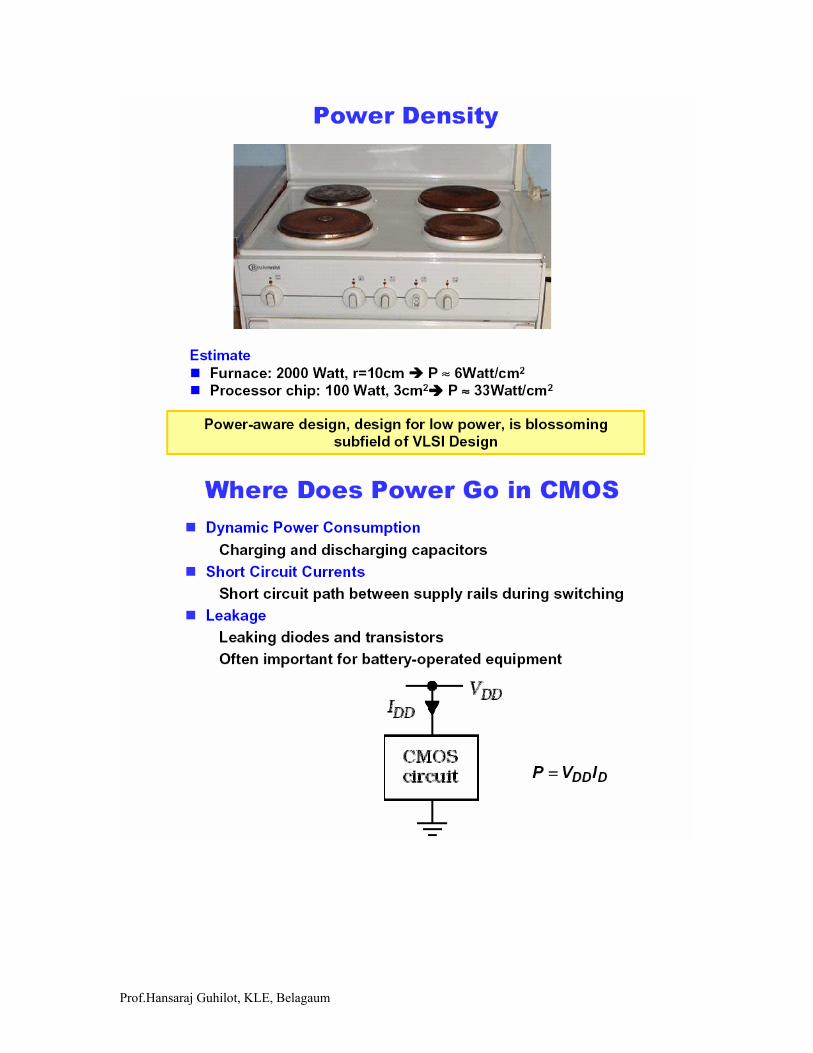
Prof.Hansaraj Guhilot, KLE, Belagaum

Prof.Hansaraj Guhilot, KLE, Belagaum

Prof.Hansaraj Guhilot, KLE, Belagaum

Prof.Hansaraj Guhilot, KLE, Belagaum

Prof.Hansaraj Guhilot, KLE, Belagaum