PSMN2R0-30YLE - Nexperia€¦ · PSMN2R0-30YLE McDkcdoNµuRu3=,muKiidoLvafdcfcdlcn Nexperia...
13
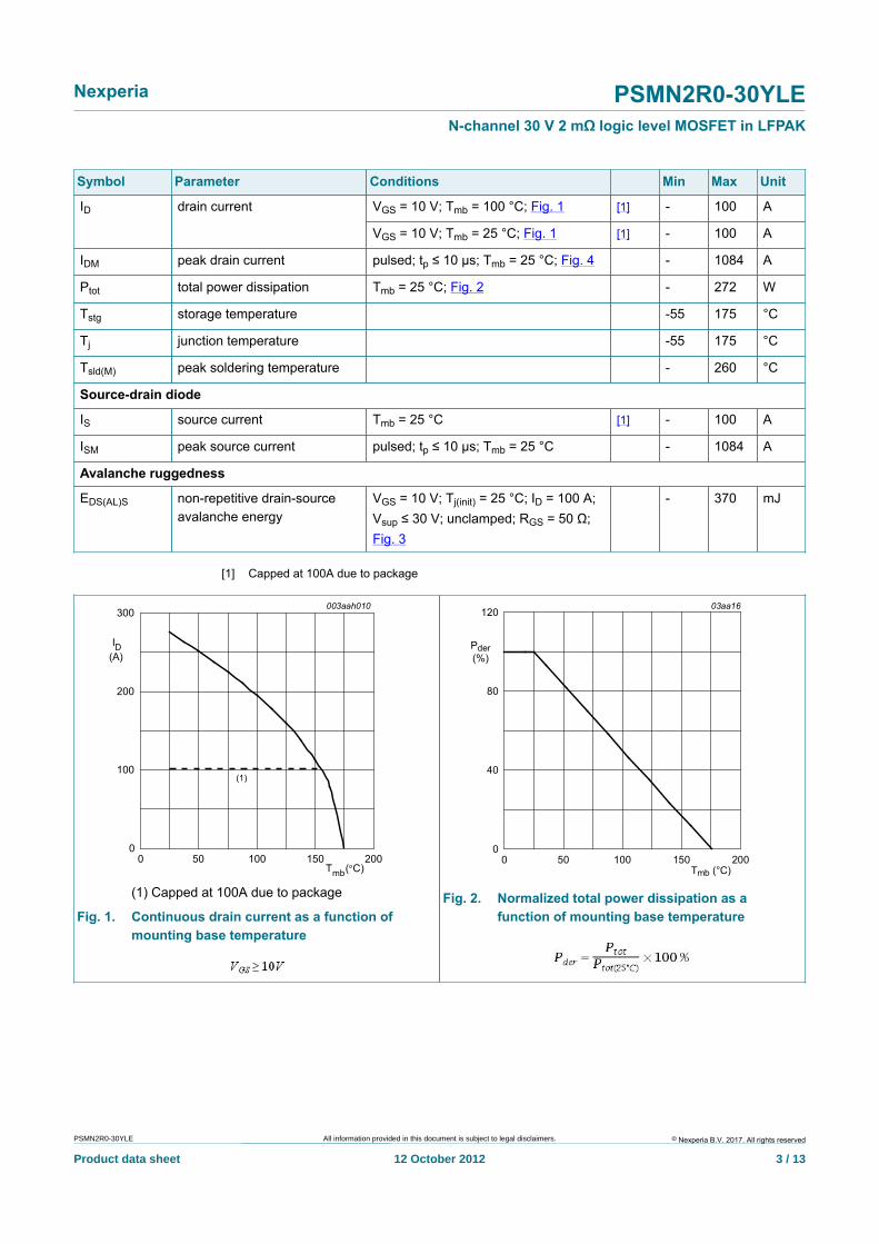
PSMN2R0-30YLE N-channel 30 V 2 mΩ logic level MOSFET in LFPAK 12 October 2012 Product data sheet 1. Product profile 1.1 General description Logic level N-channel MOSFET in LFPAK package qualified to 175 °C. This product is designed and qualified for use in a wide range of industrial, communications and domestic equipment. 1.2 Features and benefits • Enhanced forward biased safe operating area for superior linear mode operation • Very low Rdson for low conduction losses 1.3 Applications • Electronic fuse • Hot swap • Load switch • Soft start 1.4 Quick reference data Table 1. Quick reference data Symbol Parameter Conditions Min Typ Max Unit V DS drain-source voltage T j ≥ 25 °C; T j ≤ 175 °C - - 30 V I D drain current T mb = 25 °C; V GS = 10 V; Fig. 1 [1] - - 100 A P tot total power dissipation T mb = 25 °C; Fig. 2 - - 272 W Static characteristics V GS = 10 V; I D = 25 A; T j = 25 °C; Fig. 12 - 1.7 2 mΩ R DSon drain-source on-state resistance V GS = 4.5 V; I D = 25 A; T j = 25 °C; Fig. 12 - 3 3.5 mΩ Dynamic characteristics Q GD gate-drain charge V GS = 4.5 V; I D = 25 A; V DS = 15 V; Fig. 14 ; Fig. 15 - 13.8 - nC Q G(tot) total gate charge V GS = 10 V; I D = 25 A; V DS = 15 V; Fig. 14 ; Fig. 15 - 87 - nC
Transcript of PSMN2R0-30YLE - Nexperia€¦ · PSMN2R0-30YLE McDkcdoNµuRu3=,muKiidoLvafdcfcdlcn Nexperia...
PSMN2R0-30YLEN-channel 30 V 2 mΩ logic level MOSFET in LFPAK12 October 2012 Product data sheet
1. Product profile
1.1 General descriptionLogic level N-channel MOSFET in LFPAK package qualified to 175 °C. This productis designed and qualified for use in a wide range of industrial, communications anddomestic equipment.
1.2 Features and benefits• Enhanced forward biased safe operating area for superior linear mode operation• Very low Rdson for low conduction losses
1.3 Applications• Electronic fuse• Hot swap• Load switch• Soft start
1.4 Quick reference dataTable 1. Quick reference dataSymbol Parameter Conditions Min Typ Max Unit
VDS drain-source voltage Tj ≥ 25 °C; Tj ≤ 175 °C - - 30 V
ID drain current Tmb = 25 °C; VGS = 10 V; Fig. 1 [1] - - 100 A
Ptot total power dissipation Tmb = 25 °C; Fig. 2 - - 272 W
Static characteristics
VGS = 10 V; ID = 25 A; Tj = 25 °C;Fig. 12
- 1.7 2 mΩRDSon drain-source on-stateresistance
VGS = 4.5 V; ID = 25 A; Tj = 25 °C;Fig. 12
- 3 3.5 mΩ
Dynamic characteristics
QGD gate-drain charge VGS = 4.5 V; ID = 25 A; VDS = 15 V;Fig. 14; Fig. 15
- 13.8 - nC
QG(tot) total gate charge VGS = 10 V; ID = 25 A; VDS = 15 V;Fig. 14; Fig. 15
- 87 - nC

© Nexperia B.V. 2017. All rights reserved
Nexperia PSMN2R0-30YLEN-channel 30 V 2 mΩ logic level MOSFET in LFPAK
PSMN2R0-30YLE All information provided in this document is subject to legal disclaimers.
Product data sheet 12 October 2012 2 / 13
Symbol Parameter Conditions Min Typ Max Unit
Avalanche ruggedness
EDS(AL)S non-repetitive drain-source avalancheenergy
VGS = 10 V; Tj(init) = 25 °C; ID = 100 A;Vsup ≤ 30 V; unclamped; RGS = 50 Ω;Fig. 3
- - 370 mJ
[1] Capped at 100A due to package
2. Pinning informationTable 2. Pinning informationPin Symbol Description Simplified outline Graphic symbol
1 S source
2 S source
3 S source
4 G gate
mb D mounting base; connected todrain
mb
1 2 3 4
LFPAK; Power-SO8 (SOT669)
S
D
G
mbb076
3. Ordering informationTable 3. Ordering information
PackageType number
Name Description Version
PSMN2R0-30YLE LFPAK;Power-SO8
plastic single-ended surface-mounted package; 4 leads SOT669
4. MarkingTable 4. Marking codesType number Marking code
PSMN2R0-30YLE 2R030
5. Limiting valuesTable 5. Limiting valuesIn accordance with the Absolute Maximum Rating System (IEC 60134).Symbol Parameter Conditions Min Max Unit
VDS drain-source voltage Tj ≥ 25 °C; Tj ≤ 175 °C - 30 V
VDGR drain-gate voltage Tj ≤ 175 °C; Tj ≥ 25 °C; RGS = 20 kΩ - 30 V
VGS gate-source voltage -20 20 V
© Nexperia B.V. 2017. All rights reserved
Nexperia PSMN2R0-30YLEN-channel 30 V 2 mΩ logic level MOSFET in LFPAK
PSMN2R0-30YLE All information provided in this document is subject to legal disclaimers.
Product data sheet 12 October 2012 3 / 13
Symbol Parameter Conditions Min Max Unit
VGS = 10 V; Tmb = 100 °C; Fig. 1 [1] - 100 AID drain current
VGS = 10 V; Tmb = 25 °C; Fig. 1 [1] - 100 A
IDM peak drain current pulsed; tp ≤ 10 µs; Tmb = 25 °C; Fig. 4 - 1084 A
Ptot total power dissipation Tmb = 25 °C; Fig. 2 - 272 W
Tstg storage temperature -55 175 °C
Tj junction temperature -55 175 °C
Tsld(M) peak soldering temperature - 260 °C
Source-drain diode
IS source current Tmb = 25 °C [1] - 100 A
ISM peak source current pulsed; tp ≤ 10 µs; Tmb = 25 °C - 1084 A
Avalanche ruggedness
EDS(AL)S non-repetitive drain-sourceavalanche energy
VGS = 10 V; Tj(init) = 25 °C; ID = 100 A;Vsup ≤ 30 V; unclamped; RGS = 50 Ω;Fig. 3
- 370 mJ
[1] Capped at 100A due to package
003aah010
0
100
200
300
0 50 100 150 200Tmb(°C)
ID(A)
(1)
(1) Capped at 100A due to package
Fig. 1. Continuous drain current as a function ofmounting base temperature
Tmb (°C)0 20015050 100
03aa16
40
80
120
Pder(%)
0
Fig. 2. Normalized total power dissipation as afunction of mounting base temperature

© Nexperia B.V. 2017. All rights reserved
Nexperia PSMN2R0-30YLEN-channel 30 V 2 mΩ logic level MOSFET in LFPAK
PSMN2R0-30YLE All information provided in this document is subject to legal disclaimers.
Product data sheet 12 October 2012 4 / 13
003aaj896
1
10
102
103
10-3 10-2 10-1 1 10tAL(ms)
IAL(A)
(1)
(2)
Fig. 3. Single pulse avalanche rating; avalanche current as a function of avalanche time
003aah012
1
10
102
103
104
10-1 1 10 102
VDS(V)
ID(A)
Limit RDSon = VDS/ ID
DC
100 µs
10 ms
tp =10 µs
100 ms
1 ms
Fig. 4. Safe operating area; continuous and peak drain currents as a function of drain-source voltage
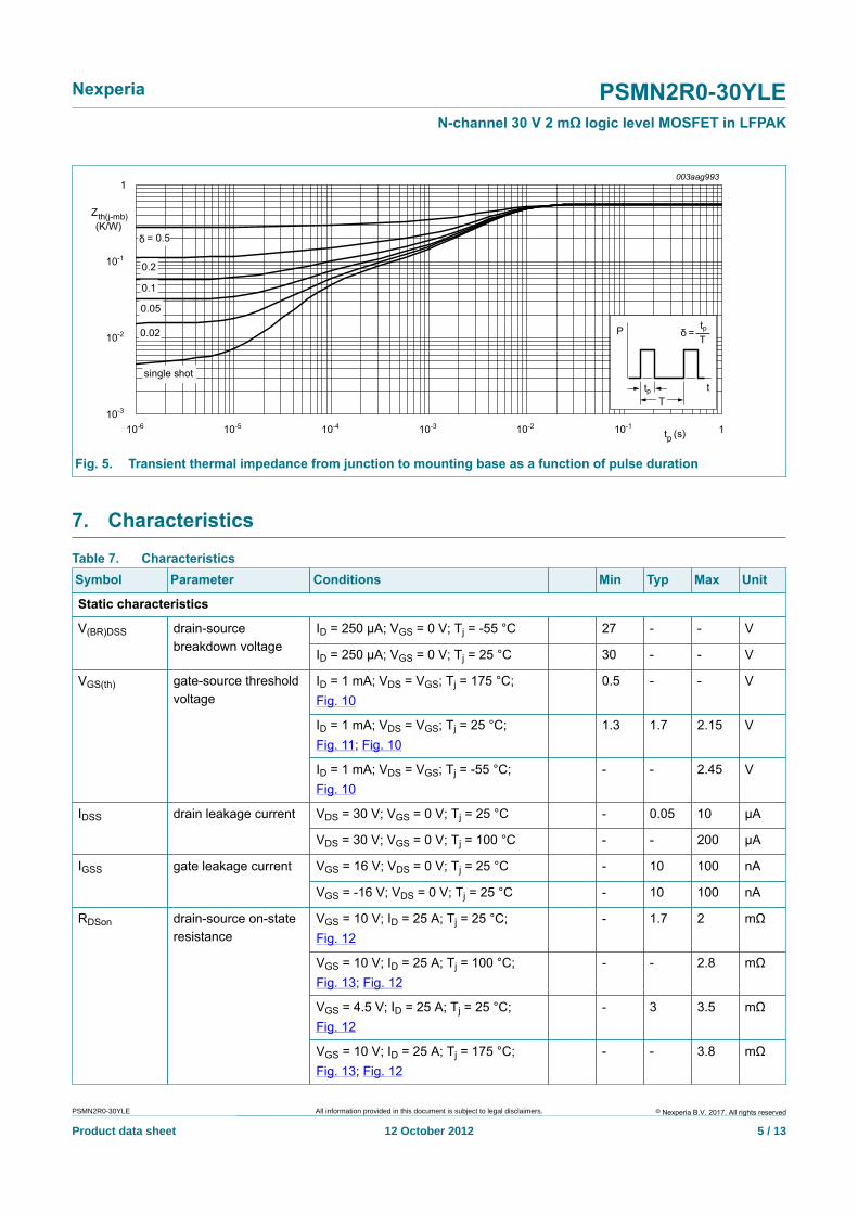
6. Thermal characteristicsTable 6. Thermal characteristicsSymbol Parameter Conditions Min Typ Max Unit
Rth(j-mb) thermal resistancefrom junction tomounting base
Fig. 5 - 0.45 0.55 K/W
© Nexperia B.V. 2017. All rights reserved
Nexperia PSMN2R0-30YLEN-channel 30 V 2 mΩ logic level MOSFET in LFPAK
PSMN2R0-30YLE All information provided in this document is subject to legal disclaimers.
Product data sheet 12 October 2012 5 / 13
003aag993
single shot
0.2
0.1
0.05
10-3
10-2
10-1
1
10-6 10-5 10-4 10-3 10-2 10-1 1tp (s)
Zth(j-mb)(K/W)
δ = 0.5
0.02
tpT
P
t
tpT
δ =
Fig. 5. Transient thermal impedance from junction to mounting base as a function of pulse duration
7. CharacteristicsTable 7. CharacteristicsSymbol Parameter Conditions Min Typ Max Unit
Static characteristics
ID = 250 µA; VGS = 0 V; Tj = -55 °C 27 - - VV(BR)DSS drain-sourcebreakdown voltage ID = 250 µA; VGS = 0 V; Tj = 25 °C 30 - - V
ID = 1 mA; VDS = VGS; Tj = 175 °C;Fig. 10
0.5 - - V
ID = 1 mA; VDS = VGS; Tj = 25 °C;Fig. 11; Fig. 10
1.3 1.7 2.15 V
VGS(th) gate-source thresholdvoltage
ID = 1 mA; VDS = VGS; Tj = -55 °C;Fig. 10
- - 2.45 V
VDS = 30 V; VGS = 0 V; Tj = 25 °C - 0.05 10 µAIDSS drain leakage current
VDS = 30 V; VGS = 0 V; Tj = 100 °C - - 200 µA
VGS = 16 V; VDS = 0 V; Tj = 25 °C - 10 100 nAIGSS gate leakage current
VGS = -16 V; VDS = 0 V; Tj = 25 °C - 10 100 nA
VGS = 10 V; ID = 25 A; Tj = 25 °C;Fig. 12
- 1.7 2 mΩ
VGS = 10 V; ID = 25 A; Tj = 100 °C;Fig. 13; Fig. 12
- - 2.8 mΩ
VGS = 4.5 V; ID = 25 A; Tj = 25 °C;Fig. 12
- 3 3.5 mΩ
RDSon drain-source on-stateresistance
VGS = 10 V; ID = 25 A; Tj = 175 °C;Fig. 13; Fig. 12
- - 3.8 mΩ
© Nexperia B.V. 2017. All rights reserved
Nexperia PSMN2R0-30YLEN-channel 30 V 2 mΩ logic level MOSFET in LFPAK
PSMN2R0-30YLE All information provided in this document is subject to legal disclaimers.
Product data sheet 12 October 2012 6 / 13
Symbol Parameter Conditions Min Typ Max Unit
RG internal gateresistance (AC)
f = 1 MHz 0.3 0.6 1.2 Ω
Dynamic characteristics
ID = 25 A; VDS = 15 V; VGS = 10 V;Fig. 14; Fig. 15
- 87 - nC
ID = 25 A; VDS = 15 V; VGS = 4.5 V;Fig. 14; Fig. 15
- 41 - nC
QG(tot) total gate charge
ID = 0 A; VDS = 0 V; VGS = 10 V - 79 - nC
QGS gate-source charge - 13.3 - nC
QGS(th) pre-threshold gate-source charge
- 8.1 - nC
QGS(th-pl) post-threshold gate-source charge
- 5.2 - nC
QGD gate-drain charge
ID = 25 A; VDS = 15 V; VGS = 4.5 V;Fig. 14; Fig. 15
- 13.8 - nC
VGS(pl) gate-source plateauvoltage
ID = 25 A; VDS = 15 V; Fig. 14; Fig. 15 - 2.8 - V
Ciss input capacitance - 5217 - pF
Coss output capacitance - 1015 - pF
Crss reverse transfercapacitance
VDS = 15 V; VGS = 0 V; f = 1 MHz;Tj = 25 °C; Fig. 16
- 474 - pF
td(on) turn-on delay time - 32.7 - ns
tr rise time - 55.7 - ns
td(off) turn-off delay time - 41.5 - ns
tf fall time
VDS = 15 V; RL = 0.6 Ω; VGS = 4.5 V;RG(ext) = 4.7 Ω; Tj = 25 °C
- 29.5 - ns
Source-drain diode
VSD source-drain voltage IS = 25 A; VGS = 0 V; Tj = 25 °C; Fig. 17 - 0.8 1.2 V
trr reverse recovery time - 42.6 - ns
Qr recovered charge
IS = 25 A; dIS/dt = 100 A/µs; VGS = 0 V;VDS = 15 V - 49.8 - nC
© Nexperia B.V. 2017. All rights reserved
Nexperia PSMN2R0-30YLEN-channel 30 V 2 mΩ logic level MOSFET in LFPAK
PSMN2R0-30YLE All information provided in this document is subject to legal disclaimers.
Product data sheet 12 October 2012 7 / 13
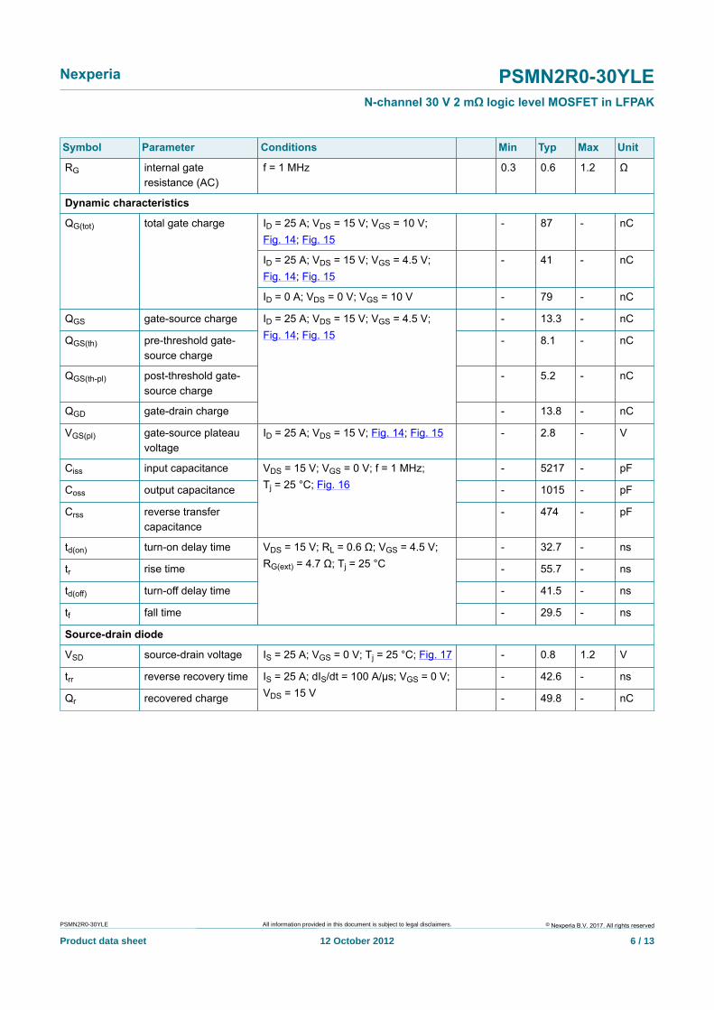
003aah014
0
20
40
60
80
100
0 0.5 1 1.5 2VDS(V)
ID(A)
VGS(V) = 3.5
2.6
2.8
4.510
2.4
3
Fig. 6. Output characteristics; drain current as afunction of drain-source voltage; typical values
003aah015
0
2
4
6
8
0 4 8 12 16VGS(V)
RDSon(mΩ)
Fig. 7. Drain-source on-state resistance as a functionof gate-source voltage; typical values
003aah016
0
30
60
90
120
150
0 20 40 60 80 100ID (A)
gfs(S)
Fig. 8. Forward transconductance as a function ofdrain current; typical values
003aah017
0
50
100
150
200
0 1 2 3 4 5VGS(V)
ID(A)
Tj = 25 °C
Tj = 175 °C
Fig. 9. Transfer characteristics; drain current as afunction of gate-source voltage; typical values
© Nexperia B.V. 2017. All rights reserved
Nexperia PSMN2R0-30YLEN-channel 30 V 2 mΩ logic level MOSFET in LFPAK
PSMN2R0-30YLE All information provided in this document is subject to legal disclaimers.
Product data sheet 12 October 2012 8 / 13
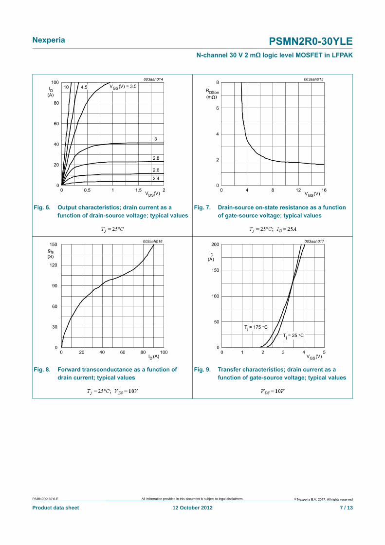
003aaj515
0
1
2
3
-60 0 60 120 180Tj (°C)
VGS(th)(V)
max
typ
min
Fig. 10. Gate-source threshold voltage as a function ofjunction temperature
003aaj514
10-6
10-5
10-4
10-3
10-2
10-1
0 1 2 3VGS(V)
ID(A)
maxtypmin
Fig. 11. Sub-threshold drain current as a function ofgate-source voltage
003aah020
0
10
20
30
10 30 50 70 90ID(A)
RDSon(mΩ)
4.5
VGS(V) = 3
10
3.5
2.8
Fig. 12. Drain-source on-state resistance as a functionof drain current; typical values
003aag820
0
0.5
1
1.5
2
-60 0 60 120 180Tj (°C)
a
Fig. 13. Normalized drain-source on-state resistancefactor as a function of junction temperature
© Nexperia B.V. 2017. All rights reserved
Nexperia PSMN2R0-30YLEN-channel 30 V 2 mΩ logic level MOSFET in LFPAK
PSMN2R0-30YLE All information provided in this document is subject to legal disclaimers.
Product data sheet 12 October 2012 9 / 13
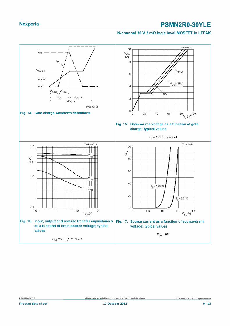
003aaa508
VGS
VGS(th)
QGS1 QGS2
QGD
VDS
QG(tot)
ID
QGS
VGS(pl)
Fig. 14. Gate charge waveform definitions
003aah022
0
2
4
6
8
10
0 20 40 60 80 100QG (nC)
VGS(V)
VDS= 15V
24 V
6 V
Fig. 15. Gate-source voltage as a function of gatecharge; typical values
003aah023
102
103
104
10-1 1 10 102
VDS(V)
C(pF)
Ciss
Crss
Coss
Fig. 16. Input, output and reverse transfer capacitancesas a function of drain-source voltage; typicalvalues
003aah024
0
20
40
60
80
100
0 0.3 0.6 0.9 1.2VSD(V)
IS(A)
Tj = 25 °C
Tj = 150°C
Fig. 17. Source current as a function of source-drainvoltage; typical values
© Nexperia B.V. 2017. All rights reserved
Nexperia PSMN2R0-30YLEN-channel 30 V 2 mΩ logic level MOSFET in LFPAK
PSMN2R0-30YLE All information provided in this document is subject to legal disclaimers.
Product data sheet 12 October 2012 10 / 13
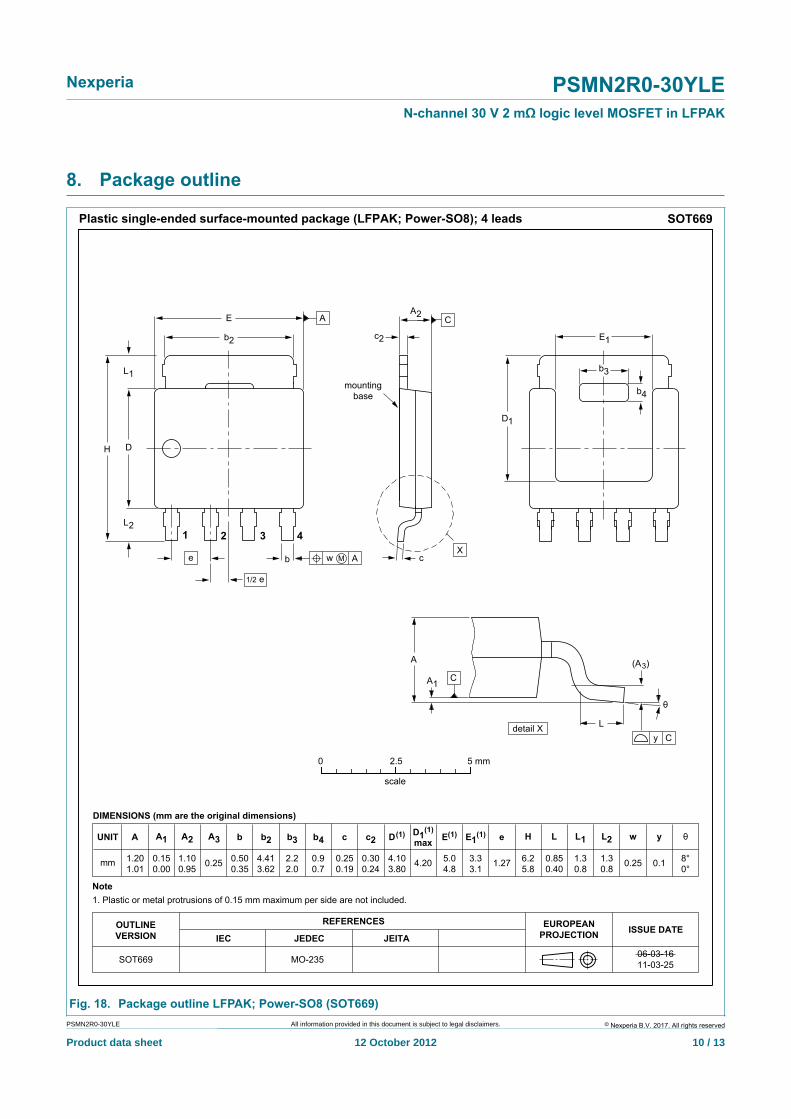
8. Package outline
REFERENCESOUTLINEVERSION
EUROPEANPROJECTION ISSUE DATE
IEC JEDEC JEITA
SOT669 MO-235 06-03-1611-03-25
0 2.5 5 mm
scale
e
E1
b
c2
A2
A2 b cA eUNIT
DIMENSIONS (mm are the original dimensions)
mm 1.100.95
A3A1
0.150.00
1.201.01
0.500.35
b2
4.413.62
b3
2.22.0
b4
0.90.7
0.250.19
c2
0.300.24
4.103.80
6.25.8
H
1.30.8
L2
0.850.40
L
1.30.8
L1
8°0°
w yD(1)
5.04.8
E(1)
3.33.1
E1(1)D1(1)
max
0.25 4.20 1.27 0.25 0.1
1 2 3 4
mountingbase
D1
c
Plastic single-ended surface-mounted package (LFPAK; Power-SO8); 4 leads SOT669
E
b2
b3
b4
H D
L2
L1
A
Aw M
C
C
X
1/2 e
y C
θ
θ
(A )3
L
A
A1
detail X
Note1. Plastic or metal protrusions of 0.15 mm maximum per side are not included.
Fig. 18. Package outline LFPAK; Power-SO8 (SOT669)
© Nexperia B.V. 2017. All rights reserved
Nexperia PSMN2R0-30YLEN-channel 30 V 2 mΩ logic level MOSFET in LFPAK
PSMN2R0-30YLE All information provided in this document is subject to legal disclaimers.
Product data sheet 12 October 2012 11 / 13
9. Legal information
9.1 Data sheet statusDocumentstatus [1][2]
Productstatus [3]
Definition
Objective[short] datasheet
Development This document contains data fromthe objective specification for productdevelopment.
Preliminary[short] datasheet
Qualification This document contains data from thepreliminary specification.
Product[short] datasheet
Production This document contains the productspecification.
[1] Please consult the most recently issued document before initiating orcompleting a design.
[2] The term 'short data sheet' is explained in section "Definitions".[3] The product status of device(s) described in this document may have
changed since this document was published and may differ in case ofmultiple devices. The latest product status information is available onthe Internet at URL http://www.nexperia.com.
9.2 DefinitionsPreview — The document is a preview version only. The document is stillsubject to formal approval, which may result in modifications or additions.Nexperia does not give any representations or warranties as tothe accuracy or completeness of information included herein and shall haveno liability for the consequences of use of such information.
Draft — The document is a draft version only. The content is still underinternal review and subject to formal approval, which may result inmodifications or additions. Nexperia does not give anyrepresentations or warranties as to the accuracy or completeness ofinformation included herein and shall have no liability for the consequencesof use of such information.
Short data sheet — A short data sheet is an extract from a full data sheetwith the same product type number(s) and title. A short data sheet isintended for quick reference only and should not be relied upon to containdetailed and full information. For detailed and full information see therelevant full data sheet, which is available on request via the local Nexperiasales office. In case of any inconsistency or conflict with theshort data sheet, the full data sheet shall prevail.
Product specification — The information and data provided in a Productdata sheet shall define the specification of the product as agreed betweenNexperia and its customer, unless Nexperia andcustomer have explicitly agreed otherwise in writing. In no event however,shall an agreement be valid in which the Nexperia productis deemed to offer functions and qualities beyond those described in theProduct data sheet.
9.3 DisclaimersLimited warranty and liability — Information in this document is believedto be accurate and reliable. However, Nexperia does not giveany representations or warranties, expressed or implied, as to the accuracyor completeness of such information and shall have no liability for theconsequences of use of such information. Nexperia takes noresponsibility for the content in this document if provided by an informationsource outside of Nexperia.
In no event shall Nexperia be liable for any indirect, incidental,punitive, special or consequential damages (including - without limitation -lost profits, lost savings, business interruption, costs related to the removalor replacement of any products or rework charges) whether or not suchdamages are based on tort (including negligence), warranty, breach ofcontract or any other legal theory.
Notwithstanding any damages that customer might incur for any reasonwhatsoever, Nexperia’s aggregate and cumulative liability towardscustomer for the products described herein shall be limited in accordancewith the Terms and conditions of commercial sale of Nexperia.
Right to make changes — Nexperia reserves the right tomake changes to information published in this document, including withoutlimitation specifications and product descriptions, at any time and withoutnotice. This document supersedes and replaces all information supplied priorto the publication hereof.
Suitability for use — Nexperia products are not designed,authorized or warranted to be suitable for use in life support, life-critical orsafety-critical systems or equipment, nor in applications where failure ormalfunction of a Nexperia product can reasonably be expectedto result in personal injury, death or severe property or environmentaldamage. Nexperia and its suppliers accept no liability forinclusion and/or use of Nexperia products in such equipment orapplications and therefore such inclusion and/or use is at the customer’s ownrisk.
Quick reference data — The Quick reference data is an extract of theproduct data given in the Limiting values and Characteristics sections of thisdocument, and as such is not complete, exhaustive or legally binding.
Applications — Applications that are described herein for any of theseproducts are for illustrative purposes only. Nexperia makes norepresentation or warranty that such applications will be suitable for thespecified use without further testing or modification.
Customers are responsible for the design and operation of theirapplications and products using Nexperia products, and Nexperiaaccepts no liability for any assistance with applications orcustomer product design. It is customer’s sole responsibility to determinewhether the Nexperia product is suitable and fit for thecustomer’s applications and products planned, as well as for the plannedapplication and use of customer’s third party customer(s). Customers shouldprovide appropriate design and operating safeguards to minimize the risksassociated with their applications and products.
Nexperia does not accept any liability related to any default,damage, costs or problem which is based on any weakness or defaultin the customer’s applications or products, or the application or use bycustomer’s third party customer(s). Customer is responsible for doing allnecessary testing for the customer’s applications and products using Nexperiaproducts in order to avoid a default of the applicationsand the products or of the application or use by customer’s third partycustomer(s). Nexperia does not accept any liability in this respect.
Limiting values — Stress above one or more limiting values (as defined inthe Absolute Maximum Ratings System of IEC 60134) will cause permanentdamage to the device. Limiting values are stress ratings only and (proper)operation of the device at these or any other conditions above thosegiven in the Recommended operating conditions section (if present) or theCharacteristics sections of this document is not warranted. Constant orrepeated exposure to limiting values will permanently and irreversibly affectthe quality and reliability of the device.
Terms and conditions of commercial sale — Nexperiaproducts are sold subject to the general terms and conditions of commercialsale, as published at http://www.nexperia.com/profile/terms, unless otherwiseagreed in a valid written individual agreement. In case an individualagreement is concluded only the terms and conditions of the respectiveagreement shall apply. Nexperia hereby expressly objects toapplying the customer’s general terms and conditions with regard to thepurchase of Nexperia products by customer.
No offer to sell or license — Nothing in this document may be interpretedor construed as an offer to sell products that is open for acceptance or the
© Nexperia B.V. 2017. All rights reserved
Nexperia PSMN2R0-30YLEN-channel 30 V 2 mΩ logic level MOSFET in LFPAK
PSMN2R0-30YLE All information provided in this document is subject to legal disclaimers.
Product data sheet 12 October 2012 12 / 13
grant, conveyance or implication of any license under any copyrights, patentsor other industrial or intellectual property rights.
Export control — This document as well as the item(s) described hereinmay be subject to export control regulations. Export might require a priorauthorization from competent authorities.
Non-automotive qualified products — Unless this data sheet expresslystates that this specific Nexperia product is automotive qualified,the product is not suitable for automotive use. It is neither qualified nortested in accordance with automotive testing or application requirements.Nexperia accepts no liability for inclusion and/or use of non-automotive qualified products in automotive equipment or applications.
In the event that customer uses the product for design-in and use inautomotive applications to automotive specifications and standards,customer (a) shall use the product without Nexperia’s warrantyof the product for such automotive applications, use and specifications, and(b) whenever customer uses the product for automotive applications beyondNexperia’s specifications such use shall be solely at customer’sown risk, and (c) customer fully indemnifies Nexperia for anyliability, damages or failed product claims resulting from customer design anduse of the product for automotive applications beyond Nexperia’sstandard warranty and Nexperia’s product specifications.
Translations — A non-English (translated) version of a document is forreference only. The English version shall prevail in case of any discrepancybetween the translated and English versions.
9.4 TrademarksNotice: All referenced brands, product names, service names andtrademarks are the property of their respective owners.

© Nexperia B.V. 2017. All rights reserved
Nexperia PSMN2R0-30YLEN-channel 30 V 2 mΩ logic level MOSFET in LFPAK
PSMN2R0-30YLE All information provided in this document is subject to legal disclaimers.
Product data sheet 12 October 2012 13 / 13
10. Contents1 Product profile ....................................................... 11.1 General description .............................................. 11.2 Features and benefits ...........................................11.3 Applications .......................................................... 11.4 Quick reference data ............................................ 12 Pinning information ...............................................23 Ordering information .............................................24 Marking ................................................................... 25 Limiting values .......................................................26 Thermal characteristics .........................................47 Characteristics .......................................................58 Package outline ................................................... 109 Legal information .................................................119.1 Data sheet status ............................................... 119.2 Definitions ...........................................................119.3 Disclaimers .........................................................119.4 Trademarks ........................................................ 12
© Nexperia B.V. 2017. All rights reservedFor more information, please visit: http://www.nexperia.comFor sales office addresses, please send an email to: [email protected] Date of release: 12 October 2012