PMDXB950UPEL - Nexperia
16
PMDXB950UPEL 20 V, dual P-channel Trench MOSFET 28 June 2016 Product data sheet 1. General description Dual P-channel enhancement mode Field-Effect Transistor (FET) in a leadless ultra small DFN1010B-6 (SOT1216) Surface-Mounted Device (SMD) plastic package using Trench MOSFET technology. 2. Features and benefits • Low leakage current • Trench MOSFET technology • Leadless ultra small and ultra thin SMD plastic package: 1.1 × 1.0 × 0.37 mm • Exposed drain pad for excellent thermal conduction • ElectroStatic Discharge (ESD) protection > 1 kV HBM • Drain-source on-state resistance R DSon = 1.02 Ω 3. Applications • Relay driver • High-speed line driver • High-side load switch • Switching circuits 4. Quick reference data Table 1. Quick reference data Symbol Parameter Conditions Min Typ Max Unit Per transistor V DS drain-source voltage - - -20 V V GS gate-source voltage T j = 25 °C -8 - 8 V I D drain current V GS = -4.5 V; T amb = 25 °C [1] - - -500 mA Static characteristics (per transistor) R DSon drain-source on-state resistance V GS = -4.5 V; I D = -500 mA; T j = 25 °C - 1.02 1.4 Ω [1] Device mounted on an FR4 Printed-Circuit Board (PCB), single-sided copper, tin-plated, mounting pad for drain 1 cm 2 .
Transcript of PMDXB950UPEL - Nexperia
PMDXB950UPEL20 V, dual P-channel Trench MOSFET28 June 2016 Product data sheet
1. General descriptionDual P-channel enhancement mode Field-Effect Transistor (FET) in a leadless ultra smallDFN1010B-6 (SOT1216) Surface-Mounted Device (SMD) plastic package using TrenchMOSFET technology.
2. Features and benefits• Low leakage current• Trench MOSFET technology• Leadless ultra small and ultra thin SMD plastic package: 1.1 × 1.0 × 0.37 mm• Exposed drain pad for excellent thermal conduction• ElectroStatic Discharge (ESD) protection > 1 kV HBM• Drain-source on-state resistance RDSon = 1.02 Ω
3. Applications• Relay driver• High-speed line driver• High-side load switch• Switching circuits
4. Quick reference dataTable 1. Quick reference dataSymbol Parameter Conditions Min Typ Max Unit
Per transistor
VDS drain-source voltage - - -20 V
VGS gate-source voltage
Tj = 25 °C
-8 - 8 V
ID drain current VGS = -4.5 V; Tamb = 25 °C [1] - - -500 mA
Static characteristics (per transistor)
RDSon drain-source on-stateresistance
VGS = -4.5 V; ID = -500 mA; Tj = 25 °C - 1.02 1.4 Ω
[1] Device mounted on an FR4 Printed-Circuit Board (PCB), single-sided copper, tin-plated, mounting pad fordrain 1 cm2.
© Nexperia B.V. 2017. All rights reserved
Nexperia PMDXB950UPEL20 V, dual P-channel Trench MOSFET
PMDXB950UPEL All information provided in this document is subject to legal disclaimers.
Product data sheet 28 June 2016 2 / 16
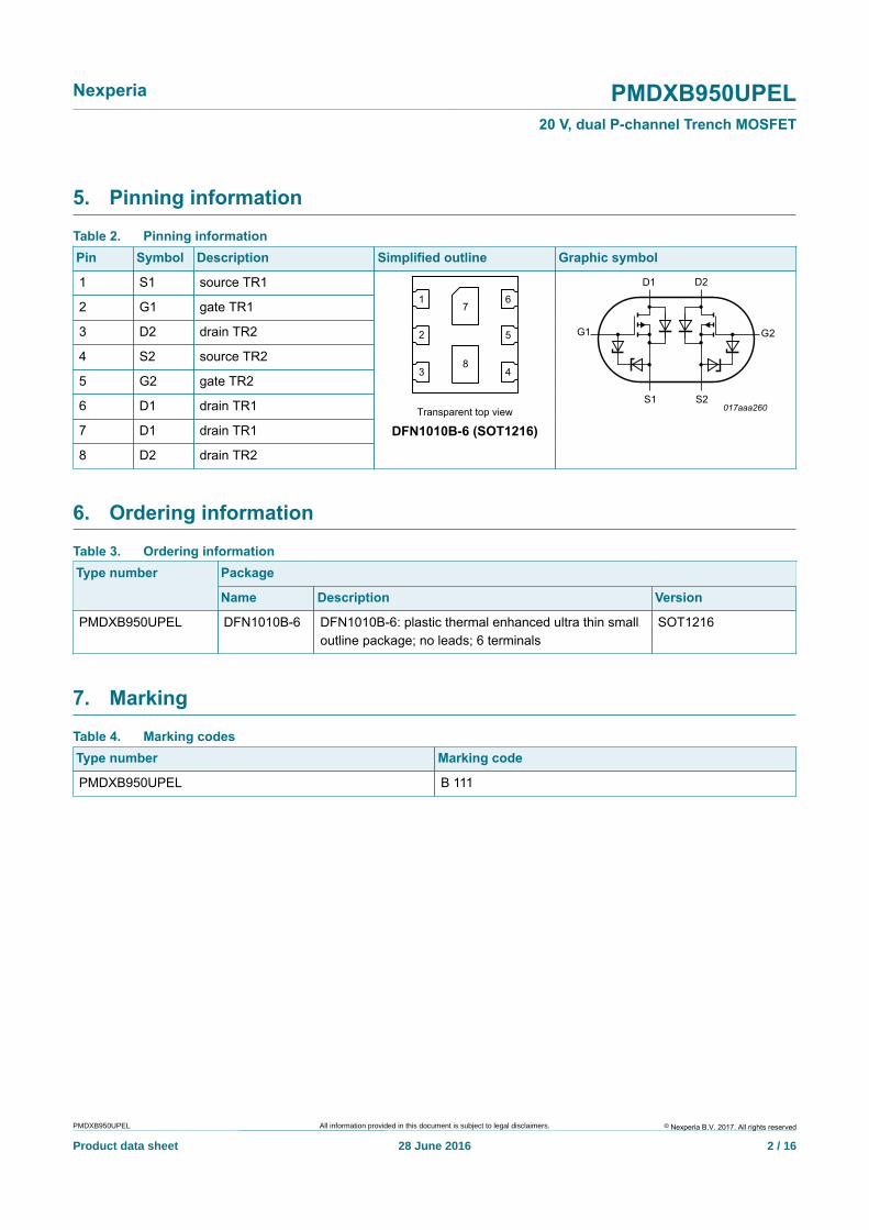
5. Pinning informationTable 2. Pinning informationPin Symbol Description Simplified outline Graphic symbol
1 S1 source TR1
2 G1 gate TR1
3 D2 drain TR2
4 S2 source TR2
5 G2 gate TR2
6 D1 drain TR1
7 D1 drain TR1
8 D2 drain TR2
Transparent top view
1 67
8
2
3
5
4
DFN1010B-6 (SOT1216)
017aaa260
D1
S1
G1
D2
S2
G2
6. Ordering informationTable 3. Ordering information
PackageType number
Name Description Version
PMDXB950UPEL DFN1010B-6 DFN1010B-6: plastic thermal enhanced ultra thin smalloutline package; no leads; 6 terminals
SOT1216
7. MarkingTable 4. Marking codesType number Marking code
PMDXB950UPEL B 111
© Nexperia B.V. 2017. All rights reserved
Nexperia PMDXB950UPEL20 V, dual P-channel Trench MOSFET
PMDXB950UPEL All information provided in this document is subject to legal disclaimers.
Product data sheet 28 June 2016 3 / 16
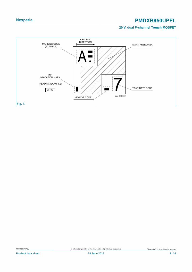
MARKING CODE(EXAMPLE)
PIN 1 INDICATION MARK
YEAR DATE CODE
READING DIRECTION
READING EXAMPLE:
A 110
aaa-019766
MARK-FREE AREA
VENDOR CODE
Fig. 1.
© Nexperia B.V. 2017. All rights reserved
Nexperia PMDXB950UPEL20 V, dual P-channel Trench MOSFET
PMDXB950UPEL All information provided in this document is subject to legal disclaimers.
Product data sheet 28 June 2016 4 / 16
8. Limiting valuesTable 5. Limiting valuesIn accordance with the Absolute Maximum Rating System (IEC 60134).Symbol Parameter Conditions Min Max Unit
Per transistor
VDS drain-source voltage - -20 V
VGS gate-source voltage
Tj = 25 °C
-8 8 V
VGS = -4.5 V; Tamb = 25 °C [1] - -500 mAID drain current
VGS = -4.5 V; Tamb = 100 °C [1] - -300 mA
IDM peak drain current Tamb = 25 °C; single pulse; tp ≤ 10 µs - -2 A
[2] - 265 mWTamb = 25 °C
[1] - 380 mW
Ptot total power dissipation
Tsp = 25 °C - 4025 mW
Per device
Tj junction temperature -55 150 °C
Tamb ambient temperature -55 150 °C
Tstg storage temperature -65 150 °C
Source-drain diode
IS source current Tamb = 25 °C [1] - -350 mA
[1] Device mounted on an FR4 Printed-Circuit Board (PCB), single-sided copper, tin-plated, mounting pad fordrain 1 cm2.
[2] Device mounted on an FR4 Printed-Circuit Board (PCB), single-sided copper, tin-plated and standardfootprint.
© Nexperia B.V. 2017. All rights reserved
Nexperia PMDXB950UPEL20 V, dual P-channel Trench MOSFET
PMDXB950UPEL All information provided in this document is subject to legal disclaimers.
Product data sheet 28 June 2016 5 / 16
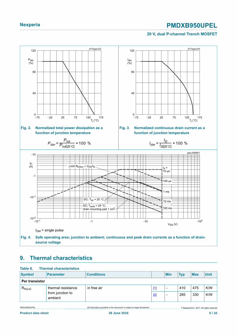
Tj (°C)- 75 17512525 75- 25
017aaa123
40
80
120
Pder(%)
0
Fig. 2. Normalized total power dissipation as afunction of junction temperature
Tj (°C)- 75 17512525 75- 25
017aaa124
40
80
120
Ider(%)
0
Fig. 3. Normalized continuous drain current as afunction of junction temperature
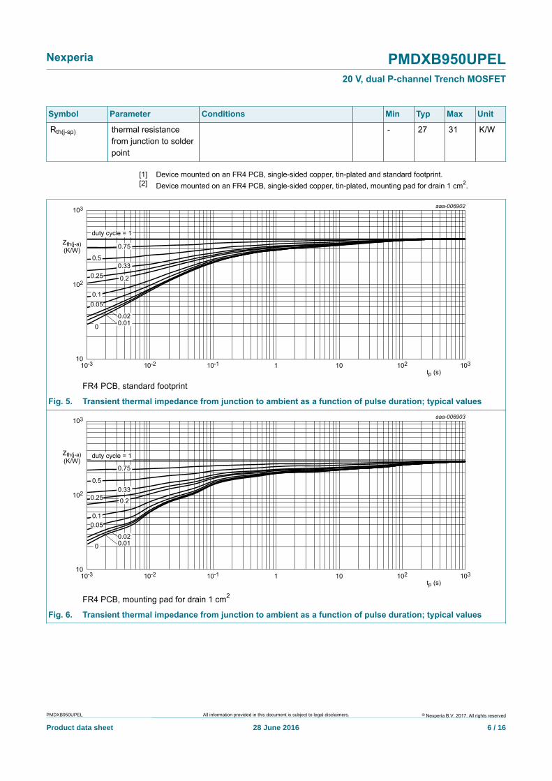
aaa-006901
VDS (V)-10-1 -102-10-1
-1
-10-1
-10
ID(A)
-10-2
100 µs
1 ms
10 msDC; Tsp = 25 °C
DC; Tamb = 25 °C;drain mounting pad 1 cm2
Limit RDSon = VDS/ID tp = 10 µs
100 ms
IDM = single pulse
Fig. 4. Safe operating area; junction to ambient; continuous and peak drain currents as a function of drain-source voltage
9. Thermal characteristicsTable 6. Thermal characteristicsSymbol Parameter Conditions Min Typ Max Unit
Per transistor
[1] - 410 475 K/WRth(j-a) thermal resistancefrom junction toambient
in free air
[2] - 285 330 K/W
© Nexperia B.V. 2017. All rights reserved
Nexperia PMDXB950UPEL20 V, dual P-channel Trench MOSFET
PMDXB950UPEL All information provided in this document is subject to legal disclaimers.
Product data sheet 28 June 2016 6 / 16
Symbol Parameter Conditions Min Typ Max Unit
Rth(j-sp) thermal resistancefrom junction to solderpoint
- 27 31 K/W
[1] Device mounted on an FR4 PCB, single-sided copper, tin-plated and standard footprint.[2] Device mounted on an FR4 PCB, single-sided copper, tin-plated, mounting pad for drain 1 cm2.
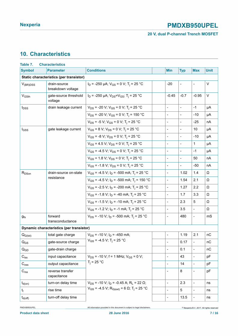
aaa-006902
tp (s)10-3 102 10310110-2 10-1
102
103
Zth(j-a)(K/W)
10
duty cycle = 1
0.75
0.50.33
0.25 0.2
0.10.05
0.020 0.01
FR4 PCB, standard footprint
Fig. 5. Transient thermal impedance from junction to ambient as a function of pulse duration; typical valuesaaa-006903
tp (s)10-3 102 10310110-2 10-1
102
103
Zth(j-a)(K/W)
10
duty cycle = 1
0.75
0.50.33
0.25 0.2
0.10.05
0.020 0.01
FR4 PCB, mounting pad for drain 1 cm2
Fig. 6. Transient thermal impedance from junction to ambient as a function of pulse duration; typical values
© Nexperia B.V. 2017. All rights reserved
Nexperia PMDXB950UPEL20 V, dual P-channel Trench MOSFET
PMDXB950UPEL All information provided in this document is subject to legal disclaimers.
Product data sheet 28 June 2016 7 / 16
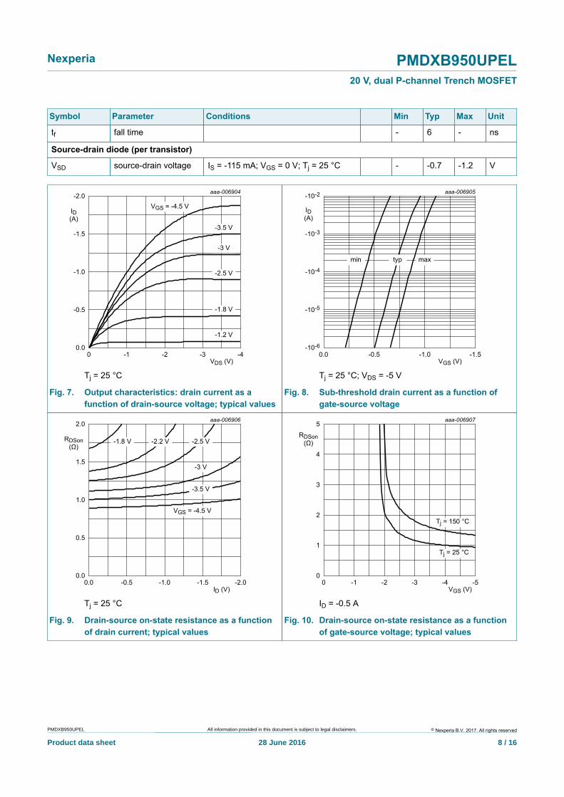
10. CharacteristicsTable 7. CharacteristicsSymbol Parameter Conditions Min Typ Max Unit
Static characteristics (per transistor)
V(BR)DSS drain-sourcebreakdown voltage
ID = -250 µA; VGS = 0 V; Tj = 25 °C -20 - - V
VGSth gate-source thresholdvoltage
ID = -250 µA; VDS=VGS; Tj = 25 °C -0.45 -0.7 -0.95 V
VDS = -20 V; VGS = 0 V; Tj = 25 °C - - -1 µA
VDS = -20 V; VGS = 0 V; Tj = 150 °C - - -10 µA
IDSS drain leakage current
VDS = -5 V; VGS = 0 V; Tj = 25 °C - - -25 nA
VGS = 8 V; VDS = 0 V; Tj = 25 °C - - 10 µA
VGS = -8 V; VDS = 0 V; Tj = 25 °C - - -10 µA
VGS = 4.5 V; VDS = 0 V; Tj = 25 °C - - 1 µA
VGS = -4.5 V; VDS = 0 V; Tj = 25 °C - - -1 µA
VGS = 1.8 V; VDS = 0 V; Tj = 25 °C - - 50 nA
IGSS gate leakage current
VGS = -1.8 V; VDS = 0 V; Tj = 25 °C - - -50 nA
VGS = -4.5 V; ID = -500 mA; Tj = 25 °C - 1.02 1.4 Ω
VGS = -4.5 V; ID = -500 mA; Tj = 150 °C - 1.54 2.1 Ω
VGS = -2.5 V; ID = -200 mA; Tj = 25 °C - 1.27 2.2 Ω
VGS = -1.8 V; ID = -40 mA; Tj = 25 °C - 1.7 3.3 Ω
VGS = -1.5 V; ID = -10 mA; Tj = 25 °C - 2.3 5 Ω
RDSon drain-source on-stateresistance
VGS = -1.2 V; ID = -1 mA; Tj = 25 °C - 3.5 - Ω
gfs forwardtransconductance
VDS = -10 V; ID = -500 mA; Tj = 25 °C - 480 - mS
Dynamic characteristics (per transistor)
QG(tot) total gate charge - 1.19 2.1 nC
QGS gate-source charge - 0.17 - nC
QGD gate-drain charge
VDS = -10 V; ID = -450 mA;VGS = -4.5 V; Tj = 25 °C
- 0.1 - nC
Ciss input capacitance - 43 - pF
Coss output capacitance - 14 - pF
Crss reverse transfercapacitance
VDS = -10 V; f = 1 MHz; VGS = 0 V;Tj = 25 °C
- 8 - pF
td(on) turn-on delay time - 2.3 - ns
tr rise time - 5 - ns
td(off) turn-off delay time
VDS = -10 V; ID = -0.45 A; RL = 22 Ω;VGS = -4.5 V; RG(ext) = 6 Ω; Tj = 25 °C
- 13.5 - ns
© Nexperia B.V. 2017. All rights reserved
Nexperia PMDXB950UPEL20 V, dual P-channel Trench MOSFET
PMDXB950UPEL All information provided in this document is subject to legal disclaimers.
Product data sheet 28 June 2016 8 / 16
Symbol Parameter Conditions Min Typ Max Unit
tf fall time - 6 - ns
Source-drain diode (per transistor)
VSD source-drain voltage IS = -115 mA; VGS = 0 V; Tj = 25 °C - -0.7 -1.2 V
VDS (V)0 -4-3-1 -2
aaa-006904
-1.0
-0.5
-1.5
-2.0
ID(A)
0.0
VGS = -4.5 V
-3.5 V
-3 V
-2.5 V
-1.8 V
-1.2 V
Tj = 25 °C
Fig. 7. Output characteristics: drain current as afunction of drain-source voltage; typical values
aaa-006905
VGS (V)0.0 -1.5-1.0-0.5
-10-5
-10-4
-10-3
-10-2
ID(A)
-10-6
min typ max
Tj = 25 °C; VDS = -5 V
Fig. 8. Sub-threshold drain current as a function ofgate-source voltage
ID (V)0.0 -2.0-1.5-0.5 -1.0
aaa-006906
1.0
0.5
1.5
2.0
RDSon(Ω)
0.0
VGS = -4.5 V
-3.5 V
-3 V
-2.5 V-1.8 V -2.2 V
Tj = 25 °C
Fig. 9. Drain-source on-state resistance as a functionof drain current; typical values
VGS (V)0 -5-4-2 -3-1
aaa-006907
2
3
1
4
5RDSon
(Ω)
0
Tj = 150 °C
Tj = 25 °C
ID = -0.5 A
Fig. 10. Drain-source on-state resistance as a functionof gate-source voltage; typical values
© Nexperia B.V. 2017. All rights reserved
Nexperia PMDXB950UPEL20 V, dual P-channel Trench MOSFET
PMDXB950UPEL All information provided in this document is subject to legal disclaimers.
Product data sheet 28 June 2016 9 / 16
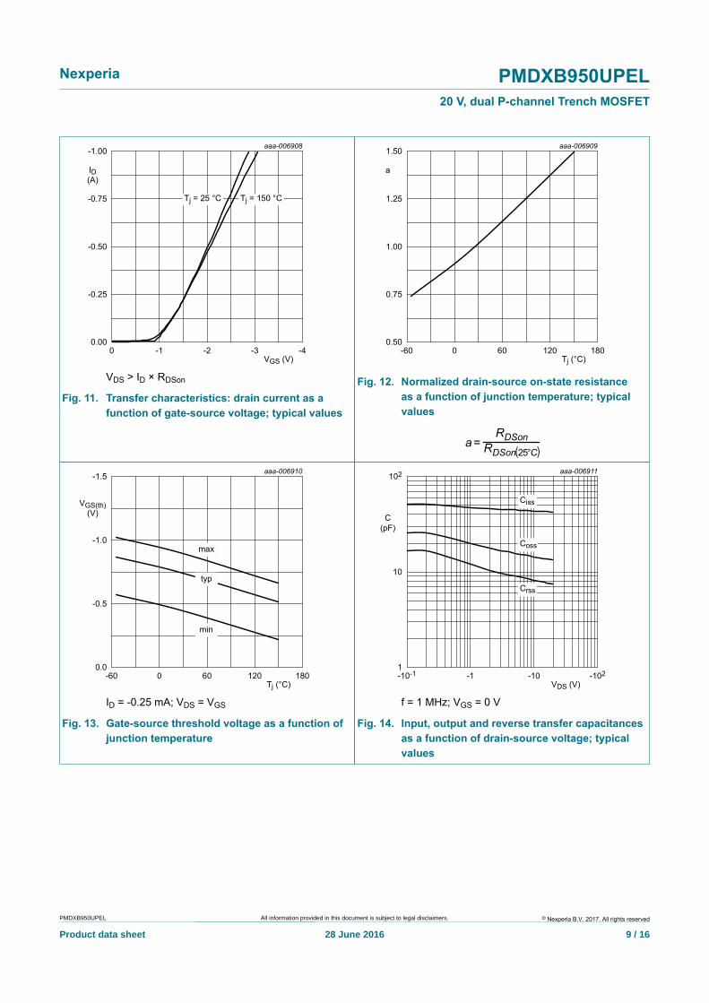
VGS (V)0 -4-3-1 -2
aaa-006908
-0.50
-0.25
-0.75
-1.00
ID(A)
0.00
Tj = 150 °CTj = 25 °C
VDS > ID × RDSon
Fig. 11. Transfer characteristics: drain current as afunction of gate-source voltage; typical values
Tj (°C)-60 1801200 60
aaa-006909
1.00
0.75
1.25
1.50
a
0.50
Fig. 12. Normalized drain-source on-state resistanceas a function of junction temperature; typicalvalues
Tj (°C)-60 1801200 60
aaa-006910
-0.5
-1.0
-1.5
VGS(th)(V)
0.0
min
typ
max
ID = -0.25 mA; VDS = VGS
Fig. 13. Gate-source threshold voltage as a function ofjunction temperature
aaa-006911
VDS (V)-10-1 -102-10-1
10
102
C(pF)
1
Ciss
Coss
Crss
f = 1 MHz; VGS = 0 V
Fig. 14. Input, output and reverse transfer capacitancesas a function of drain-source voltage; typicalvalues
© Nexperia B.V. 2017. All rights reserved
Nexperia PMDXB950UPEL20 V, dual P-channel Trench MOSFET
PMDXB950UPEL All information provided in this document is subject to legal disclaimers.
Product data sheet 28 June 2016 10 / 16
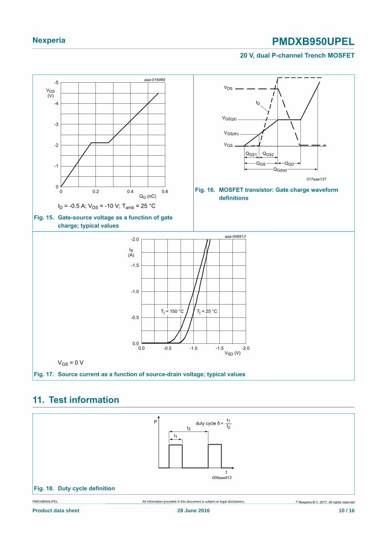
aaa-016469
QG (nC)0 0.60.40.2
-2
-3
-1
-4
-5VGS(V)
0
ID = -0.5 A; VDS = -10 V; Tamb = 25 °C
Fig. 15. Gate-source voltage as a function of gatecharge; typical values
017aaa137
VGS
VGS(th)
QGS1 QGS2
QGD
VDS
QG(tot)
ID
QGS
VGS(pl)
Fig. 16. MOSFET transistor: Gate charge waveformdefinitions
VSD (V)0.0 -2.0-1.5-0.5 -1.0
aaa-006913
-1.0
-0.5
-1.5
-2.0
IS(A)
0.0
Tj = 150 °C Tj = 25 °C
VGS = 0 V
Fig. 17. Source current as a function of source-drain voltage; typical values
11. Test information
t1t2
P
t006aaa812
duty cycle δ =
t1
t2
Fig. 18. Duty cycle definition
© Nexperia B.V. 2017. All rights reserved
Nexperia PMDXB950UPEL20 V, dual P-channel Trench MOSFET
PMDXB950UPEL All information provided in this document is subject to legal disclaimers.
Product data sheet 28 June 2016 11 / 16
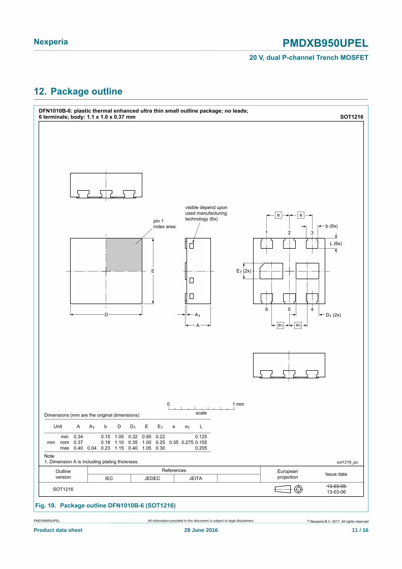
12. Package outline
ReferencesOutlineversion
Europeanprojection Issue date
IEC JEDEC JEITA
SOT1216
sot1216_po
13-03-0513-03-06
Unit
mmminnommax
1.05 0.320.1550.125
0.205
A
Dimensions (mm are the original dimensions)
Note1. Dimension A is including plating thickness.
DFN1010B-6: plastic thermal enhanced ultra thin small outline package; no leads;6 terminals; body: 1.1 x 1.0 x 0.37 mm SOT1216
A1 b
0.15
D D1 e e1 L
0.400.370.34
0.04 1.151.10
0.400.230.18
scale
0 1 mm
0.95
1.05
E E1
0.22
0.300.2750.350.35 1.00 0.25
b (6x)
e epin 1index area
visible depend uponused manufacturingtechnology (6x)
D
L (6x)
D1 (2x)
E
A1
A
E1 (2x)
1 32
56 4
e1 e1
Fig. 19. Package outline DFN1010B-6 (SOT1216)
© Nexperia B.V. 2017. All rights reserved
Nexperia PMDXB950UPEL20 V, dual P-channel Trench MOSFET
PMDXB950UPEL All information provided in this document is subject to legal disclaimers.
Product data sheet 28 June 2016 12 / 16
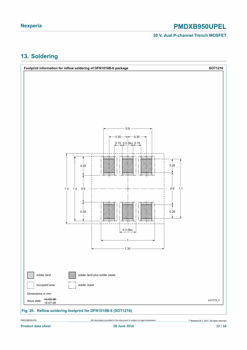
13. Soldering
SOT1216Footprint information for reflow soldering of DFN1010B-6 package
sot1216_fr
solder land
solder resist
solder land plus solder paste
occupied area
Dimensions in mm
Issue date 13-03-0614-07-28
0.3 (6x)
1.10.6
0.250.35
0.35
0.51.21.3
0.25
1
1.35
0.35
0.15 0.150.2 (6x)
0.35
0.9
Fig. 20. Reflow soldering footprint for DFN1010B-6 (SOT1216)
© Nexperia B.V. 2017. All rights reserved
Nexperia PMDXB950UPEL20 V, dual P-channel Trench MOSFET
PMDXB950UPEL All information provided in this document is subject to legal disclaimers.
Product data sheet 28 June 2016 13 / 16
14. Revision historyTable 8. Revision historyData sheet ID Release date Data sheet status Change notice Supersedes
PMDXB950UPEL v.1 20160628 Product data sheet - -
© Nexperia B.V. 2017. All rights reserved
Nexperia PMDXB950UPEL20 V, dual P-channel Trench MOSFET
PMDXB950UPEL All information provided in this document is subject to legal disclaimers.
Product data sheet 28 June 2016 14 / 16
15. Legal information
15.1 Data sheet statusDocumentstatus [1][2]
Productstatus [3]
Definition
Objective[short] datasheet
Development This document contains data fromthe objective specification for productdevelopment.
Preliminary[short] datasheet
Qualification This document contains data from thepreliminary specification.
Product[short] datasheet
Production This document contains the productspecification.
[1] Please consult the most recently issued document before initiating orcompleting a design.
[2] The term 'short data sheet' is explained in section "Definitions".[3] The product status of device(s) described in this document may have
changed since this document was published and may differ in case ofmultiple devices. The latest product status information is available onthe Internet at URL http://www.nexperia.com.
15.2 DefinitionsPreview — The document is a preview version only. The document is stillsubject to formal approval, which may result in modifications or additions.Nexperia does not give any representations or warranties as tothe accuracy or completeness of information included herein and shall haveno liability for the consequences of use of such information.
Draft — The document is a draft version only. The content is still underinternal review and subject to formal approval, which may result inmodifications or additions. Nexperia does not give anyrepresentations or warranties as to the accuracy or completeness ofinformation included herein and shall have no liability for the consequencesof use of such information.
Short data sheet — A short data sheet is an extract from a full data sheetwith the same product type number(s) and title. A short data sheet isintended for quick reference only and should not be relied upon to containdetailed and full information. For detailed and full information see therelevant full data sheet, which is available on request via the local Nexperiasales office. In case of any inconsistency or conflict with theshort data sheet, the full data sheet shall prevail.
Product specification — The information and data provided in a Productdata sheet shall define the specification of the product as agreed betweenNexperia and its customer, unless Nexperia andcustomer have explicitly agreed otherwise in writing. In no event however,shall an agreement be valid in which the Nexperia productis deemed to offer functions and qualities beyond those described in theProduct data sheet.
15.3 DisclaimersLimited warranty and liability — Information in this document is believedto be accurate and reliable. However, Nexperia does not giveany representations or warranties, expressed or implied, as to the accuracyor completeness of such information and shall have no liability for theconsequences of use of such information. Nexperia takes noresponsibility for the content in this document if provided by an informationsource outside of Nexperia.
In no event shall Nexperia be liable for any indirect, incidental,punitive, special or consequential damages (including - without limitation -lost profits, lost savings, business interruption, costs related to the removalor replacement of any products or rework charges) whether or not suchdamages are based on tort (including negligence), warranty, breach ofcontract or any other legal theory.
Notwithstanding any damages that customer might incur for any reasonwhatsoever, Nexperia’s aggregate and cumulative liability towardscustomer for the products described herein shall be limited in accordancewith the Terms and conditions of commercial sale of Nexperia.
Right to make changes — Nexperia reserves the right tomake changes to information published in this document, including withoutlimitation specifications and product descriptions, at any time and withoutnotice. This document supersedes and replaces all information supplied priorto the publication hereof.
Suitability for use — Nexperia products are not designed,authorized or warranted to be suitable for use in life support, life-critical orsafety-critical systems or equipment, nor in applications where failure ormalfunction of a Nexperia product can reasonably be expectedto result in personal injury, death or severe property or environmentaldamage. Nexperia and its suppliers accept no liability forinclusion and/or use of Nexperia products in such equipment orapplications and therefore such inclusion and/or use is at the customer’s ownrisk.
Quick reference data — The Quick reference data is an extract of theproduct data given in the Limiting values and Characteristics sections of thisdocument, and as such is not complete, exhaustive or legally binding.
Applications — Applications that are described herein for any of theseproducts are for illustrative purposes only. Nexperia makes norepresentation or warranty that such applications will be suitable for thespecified use without further testing or modification.
Customers are responsible for the design and operation of theirapplications and products using Nexperia products, and Nexperiaaccepts no liability for any assistance with applications orcustomer product design. It is customer’s sole responsibility to determinewhether the Nexperia product is suitable and fit for thecustomer’s applications and products planned, as well as for the plannedapplication and use of customer’s third party customer(s). Customers shouldprovide appropriate design and operating safeguards to minimize the risksassociated with their applications and products.
Nexperia does not accept any liability related to any default,damage, costs or problem which is based on any weakness or defaultin the customer’s applications or products, or the application or use bycustomer’s third party customer(s). Customer is responsible for doing allnecessary testing for the customer’s applications and products using Nexperiaproducts in order to avoid a default of the applicationsand the products or of the application or use by customer’s third partycustomer(s). Nexperia does not accept any liability in this respect.
Limiting values — Stress above one or more limiting values (as defined inthe Absolute Maximum Ratings System of IEC 60134) will cause permanentdamage to the device. Limiting values are stress ratings only and (proper)operation of the device at these or any other conditions above thosegiven in the Recommended operating conditions section (if present) or theCharacteristics sections of this document is not warranted. Constant orrepeated exposure to limiting values will permanently and irreversibly affectthe quality and reliability of the device.
Terms and conditions of commercial sale — Nexperiaproducts are sold subject to the general terms and conditions of commercialsale, as published at http://www.nexperia.com/profile/terms, unless otherwiseagreed in a valid written individual agreement. In case an individualagreement is concluded only the terms and conditions of the respectiveagreement shall apply. Nexperia hereby expressly objects toapplying the customer’s general terms and conditions with regard to thepurchase of Nexperia products by customer.
No offer to sell or license — Nothing in this document may be interpretedor construed as an offer to sell products that is open for acceptance or the
© Nexperia B.V. 2017. All rights reserved
Nexperia PMDXB950UPEL20 V, dual P-channel Trench MOSFET
PMDXB950UPEL All information provided in this document is subject to legal disclaimers.
Product data sheet 28 June 2016 15 / 16
grant, conveyance or implication of any license under any copyrights, patentsor other industrial or intellectual property rights.
Export control — This document as well as the item(s) described hereinmay be subject to export control regulations. Export might require a priorauthorization from competent authorities.
Non-automotive qualified products — Unless this data sheet expresslystates that this specific Nexperia product is automotive qualified,the product is not suitable for automotive use. It is neither qualified nortested in accordance with automotive testing or application requirements.Nexperia accepts no liability for inclusion and/or use of non-automotive qualified products in automotive equipment or applications.
In the event that customer uses the product for design-in and use inautomotive applications to automotive specifications and standards,customer (a) shall use the product without Nexperia’s warrantyof the product for such automotive applications, use and specifications, and(b) whenever customer uses the product for automotive applications beyondNexperia’s specifications such use shall be solely at customer’sown risk, and (c) customer fully indemnifies Nexperia for anyliability, damages or failed product claims resulting from customer design anduse of the product for automotive applications beyond Nexperia’sstandard warranty and Nexperia’s product specifications.
Translations — A non-English (translated) version of a document is forreference only. The English version shall prevail in case of any discrepancybetween the translated and English versions.
15.4 TrademarksNotice: All referenced brands, product names, service names andtrademarks are the property of their respective owners.
© Nexperia B.V. 2017. All rights reserved
Nexperia PMDXB950UPEL20 V, dual P-channel Trench MOSFET
PMDXB950UPEL All information provided in this document is subject to legal disclaimers.
Product data sheet 28 June 2016 16 / 16
16. Contents1 General description ............................................... 12 Features and benefits ............................................13 Applications ........................................................... 14 Quick reference data ............................................. 15 Pinning information ...............................................26 Ordering information .............................................27 Marking ................................................................... 28 Limiting values .......................................................49 Thermal characteristics .........................................510 Characteristics .......................................................711 Test information ................................................... 1012 Package outline ................................................... 1113 Soldering .............................................................. 1214 Revision history ...................................................1315 Legal information .................................................1415.1 Data sheet status ............................................... 1415.2 Definitions ...........................................................1415.3 Disclaimers .........................................................1415.4 Trademarks ........................................................ 15
© Nexperia B.V. 2017. All rights reservedFor more information, please visit: http://www.nexperia.comFor sales office addresses, please send an email to: [email protected] Date of release: 28 June 2016