BCM846BS - Nexperia
12
BCM846BS NPN/NPN matched double transistor 26 June 2015 Product data sheet 1. General description NPN/NPN matched double transistor in a very small SOT363 (TSSOP6) Surface- Mounted Device (SMD) plastic package. The transistors are fully isolated internally. 2. Features and benefits • Current gain matching • Base-emitter voltage matching • Drop-in replacement for standard double transistors • AEC-Q101 qualified 3. Applications • Current mirror • Differential amplifier 4. Quick reference data Table 1. Quick reference data Symbol Parameter Conditions Min Typ Max Unit Per transistor V CEO collector-emitter voltage open base - - 65 V I C collector current - - 100 mA Per transistor h FE DC current gain V CE = 5 V; I C = 2 mA; T amb = 25 °C 200 290 450 Per device h FE1 /h FE2 h FE matching [1] 0.9 1 - V BE1 −V BE2 V BE matching V CE = 5 V; I C = 2 mA; T amb = 25 °C [2] - - 2 mV [1] The smaller of the two values is taken as numerator. [2] The smaller of the two values is subtracted from the larger value.
Transcript of BCM846BS - Nexperia

BCM846BSNPN/NPN matched double transistor26 June 2015 Product data sheet
1. General descriptionNPN/NPN matched double transistor in a very small SOT363 (TSSOP6) Surface-Mounted Device (SMD) plastic package. The transistors are fully isolated internally.
2. Features and benefits• Current gain matching• Base-emitter voltage matching• Drop-in replacement for standard double transistors• AEC-Q101 qualified
3. Applications• Current mirror• Differential amplifier
4. Quick reference dataTable 1. Quick reference dataSymbol Parameter Conditions Min Typ Max Unit
Per transistor
VCEO collector-emittervoltage
open base - - 65 V
IC collector current - - 100 mA
Per transistor
hFE DC current gain VCE = 5 V; IC = 2 mA; Tamb = 25 °C 200 290 450
Per device
hFE1/hFE2 hFE matching [1] 0.9 1 -
VBE1−VBE2 VBE matching
VCE = 5 V; IC = 2 mA; Tamb = 25 °C
[2] - - 2 mV
[1] The smaller of the two values is taken as numerator.[2] The smaller of the two values is subtracted from the larger value.

© Nexperia B.V. 2017. All rights reserved
Nexperia BCM846BSNPN/NPN matched double transistor
BCM846BS All information provided in this document is subject to legal disclaimers.
Product data sheet 26 June 2015 2 / 12
5. Pinning informationTable 2. Pinning informationPin Symbol Description Simplified outline Graphic symbol
1 E emitter TR1
2 B base TR1
3 C collector TR2
4 E emitter TR2
5 B base TR2
6 C collector TR1
1 32
456
TSSOP6 (SOT363)sym020
21 3
56
TR1TR2
4
6. Ordering informationTable 3. Ordering information
PackageType number
Name Description Version
BCM846BS TSSOP6 plastic surface-mounted package; 6 leads SOT363
7. MarkingTable 4. Marking codesType number Marking code
[1]
BCM846BS F2%
[1] % = placeholder for manufacturing site code

© Nexperia B.V. 2017. All rights reserved
Nexperia BCM846BSNPN/NPN matched double transistor
BCM846BS All information provided in this document is subject to legal disclaimers.
Product data sheet 26 June 2015 3 / 12
8. Limiting valuesTable 5. Limiting valuesIn accordance with the Absolute Maximum Rating System (IEC 60134).Symbol Parameter Conditions Min Max Unit
Per transistor
VCBO collector-base voltage open emitter - 80 V
VCEO collector-emitter voltage open base - 65 V
VEBO emitter-base voltage open collector - 6 V
IC collector current - 100 mA
ICM peak collector current single pulse; tp ≤ 1 ms - 200 mA
Ptot total power dissipation Tamb ≤ 25 °C [1] - 200 mW
Per device
Ptot total power dissipation Tamb ≤ 25 °C [1] - 300 mW
Tj junction temperature - 150 °C
Tamb ambient temperature -55 150 °C
Tstg storage temperature -65 150 °C
[1] Device mounted on an FR4 Printed-Circuit Board (PCB), single-sided copper, tin-plated and standardfootprint.
9. Thermal characteristicsTable 6. Thermal characteristicsSymbol Parameter Conditions Min Typ Max Unit
Per transistor
Rth(j-a) thermal resistancefrom junction toambient
in free air [1] - - 625 K/W
Per device
Rth(j-a) thermal resistancefrom junction toambient
in free air [1] - - 416 K/W
[1] Device mounted on an FR4 PCB, single-sided copper, tin-plated and standard footprint.
© Nexperia B.V. 2017. All rights reserved
Nexperia BCM846BSNPN/NPN matched double transistor
BCM846BS All information provided in this document is subject to legal disclaimers.
Product data sheet 26 June 2015 4 / 12
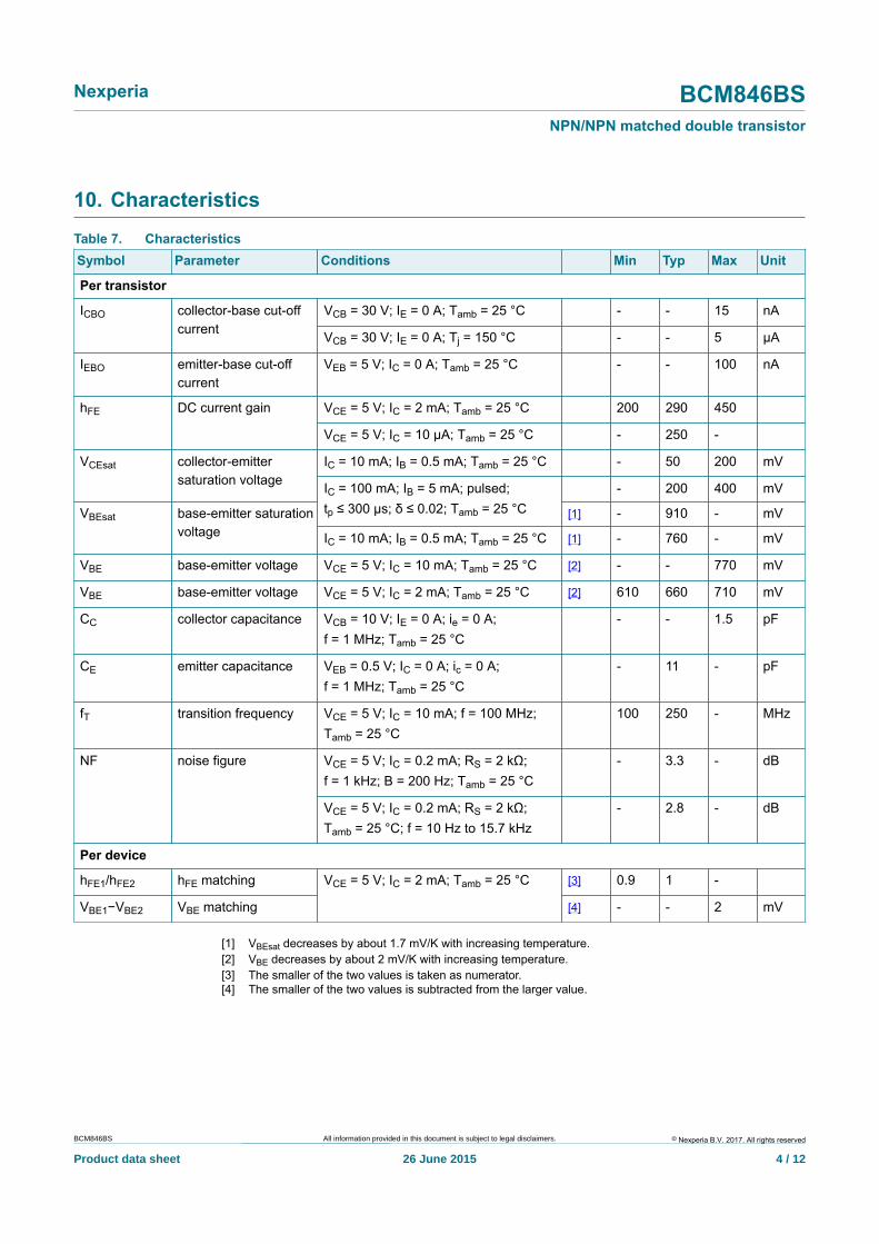
10. CharacteristicsTable 7. CharacteristicsSymbol Parameter Conditions Min Typ Max Unit
Per transistor
VCB = 30 V; IE = 0 A; Tamb = 25 °C - - 15 nAICBO collector-base cut-offcurrent VCB = 30 V; IE = 0 A; Tj = 150 °C - - 5 µA
IEBO emitter-base cut-offcurrent
VEB = 5 V; IC = 0 A; Tamb = 25 °C - - 100 nA
VCE = 5 V; IC = 2 mA; Tamb = 25 °C 200 290 450hFE DC current gain
VCE = 5 V; IC = 10 µA; Tamb = 25 °C - 250 -
IC = 10 mA; IB = 0.5 mA; Tamb = 25 °C - 50 200 mVVCEsat collector-emittersaturation voltage - 200 400 mVIC = 100 mA; IB = 5 mA; pulsed;
tp ≤ 300 µs; δ ≤ 0.02; Tamb = 25 °C [1] - 910 - mVVBEsat base-emitter saturationvoltage IC = 10 mA; IB = 0.5 mA; Tamb = 25 °C [1] - 760 - mV
VBE base-emitter voltage VCE = 5 V; IC = 10 mA; Tamb = 25 °C [2] - - 770 mV
VBE base-emitter voltage VCE = 5 V; IC = 2 mA; Tamb = 25 °C [2] 610 660 710 mV
CC collector capacitance VCB = 10 V; IE = 0 A; ie = 0 A;f = 1 MHz; Tamb = 25 °C
- - 1.5 pF
CE emitter capacitance VEB = 0.5 V; IC = 0 A; ic = 0 A;f = 1 MHz; Tamb = 25 °C
- 11 - pF
fT transition frequency VCE = 5 V; IC = 10 mA; f = 100 MHz;Tamb = 25 °C
100 250 - MHz
VCE = 5 V; IC = 0.2 mA; RS = 2 kΩ;f = 1 kHz; B = 200 Hz; Tamb = 25 °C
- 3.3 - dBNF noise figure
VCE = 5 V; IC = 0.2 mA; RS = 2 kΩ;Tamb = 25 °C; f = 10 Hz to 15.7 kHz
- 2.8 - dB
Per device
hFE1/hFE2 hFE matching [3] 0.9 1 -
VBE1−VBE2 VBE matching
VCE = 5 V; IC = 2 mA; Tamb = 25 °C
[4] - - 2 mV
[1] VBEsat decreases by about 1.7 mV/K with increasing temperature.[2] VBE decreases by about 2 mV/K with increasing temperature.[3] The smaller of the two values is taken as numerator.[4] The smaller of the two values is subtracted from the larger value.

© Nexperia B.V. 2017. All rights reserved
Nexperia BCM846BSNPN/NPN matched double transistor
BCM846BS All information provided in this document is subject to legal disclaimers.
Product data sheet 26 June 2015 5 / 12
006aaa533
200
400
600
hFE
0
IC (mA)10- 2 10310210- 1 101
(3)
(1)
(2)
VCE = 5 V(1) Tamb = 100 °C(2) Tamb = 25 °C(3) Tamb = −55 °C
Fig. 1. DC current gain as a function of collectorcurrent; typical values
006aaa532
VCE (V)0 1084 62
0.08
0.12
0.04
0.16
0.20IC(A)
0
IB (mA) = 4.50
2.703.15
4.053.60
0.45
0.90
1.351.802.25
Tamb = 25 °C
Fig. 2. Collector current as a function of collector-emitter voltage; typical values
006aaa536
0.6
0.8
1
VBE(V)
0.4
IC (mA)10- 1 1031021 10
VCE = 5 V; Tamb = 25 °C
Fig. 3. Base-emitter voltage as a function of collectorcurrent; typical values
006aaa534
IC (mA)10- 1 1031021 10
0.5
0.9
1.3
0.3
0.7
1.1
VBEsat(V)
0.1
(1)
(2)
(3)
IC/IB = 20(1) Tamb = −55 °C(2) Tamb = 25 °C(3) Tamb = 100 °C
Fig. 4. Base-emitter saturation voltage as a function ofcollector current; typical values

© Nexperia B.V. 2017. All rights reserved
Nexperia BCM846BSNPN/NPN matched double transistor
BCM846BS All information provided in this document is subject to legal disclaimers.
Product data sheet 26 June 2015 6 / 12
006aaa535
1
10- 1
10
VCEsat(V)
10- 2
IC (mA)10- 1 1031021 10
(1)
(2)(3)
IC/IB = 20(1) Tamb = 100 °C(2) Tamb = 25 °C(3) Tamb = −55 °C
Fig. 5. Collector-emitter saturation voltage as afunction of collector current; typical values
006aaa537
IC (mA)1 10210
102
103
fT(MHz)
10
VCE = 5 V; Tamb = 25 °C
Fig. 6. Transition frequency as a function of collectorcurrent; typical values
006aaa538
VCB (V)0 1084 62
2
1
3
5
4
Cc(pF)
0
f = 1 MHz; Tamb = 25 °C
Fig. 7. Collector capacitance as a function of collector-base voltage; typical values
006aaa539
VEB (V)0 642
9
11
7
13
15Ce
(pF)
5
f = 1 MHz; Tamb = 25 °C
Fig. 8. Emitter capacitance as a function of emitter-base voltage; typical values

© Nexperia B.V. 2017. All rights reserved
Nexperia BCM846BSNPN/NPN matched double transistor
BCM846BS All information provided in this document is subject to legal disclaimers.
Product data sheet 26 June 2015 7 / 12
11. Package outline
0.250.10
0.30.2
pin 1index
1.30.65
2.22.0
1.351.15
2.21.8
1.10.8
0.450.15
1 32
46 5
14-10-03Dimensions in mm
Fig. 9. Package outline TSSOP6 (SOT363)
12. Soldering
solder lands
solder resist
occupied area
solder paste
sot363_fr
2.65
2.35 0.4 (2×)
0.6(2×)
0.5(4×)
0.5(4×)
0.6(4×)
0.6(4×)
1.5
1.8
Dimensions in mm
Fig. 10. Reflow soldering footprint for TSSOP6 (SOT363)

© Nexperia B.V. 2017. All rights reserved
Nexperia BCM846BSNPN/NPN matched double transistor
BCM846BS All information provided in this document is subject to legal disclaimers.
Product data sheet 26 June 2015 8 / 12
sot363_fw
solder lands
solder resist
occupied area
preferred transportdirection during soldering
5.3
1.3 1.3
1.5
0.3
1.5
4.5
2.45
2.5
Dimensions in mm
Fig. 11. Wave soldering footprint for TSSOP6 (SOT363)

© Nexperia B.V. 2017. All rights reserved
Nexperia BCM846BSNPN/NPN matched double transistor
BCM846BS All information provided in this document is subject to legal disclaimers.
Product data sheet 26 June 2015 9 / 12
13. Revision historyTable 8. Revision historyData sheet ID Release date Data sheet status Change notice Supersedes
BCM846BS v.2 20150626 Product data sheet - BCM846BS v.1
Modification: • Product status changed
BCM846BS v.1 20150424 Objective data sheet - -

© Nexperia B.V. 2017. All rights reserved
Nexperia BCM846BSNPN/NPN matched double transistor
BCM846BS All information provided in this document is subject to legal disclaimers.
Product data sheet 26 June 2015 10 / 12
14. Legal information
14.1 Data sheet statusDocumentstatus [1][2]
Productstatus [3]
Definition
Objective[short] datasheet
Development This document contains data fromthe objective specification for productdevelopment.
Preliminary[short] datasheet
Qualification This document contains data from thepreliminary specification.
Product[short] datasheet
Production This document contains the productspecification.
[1] Please consult the most recently issued document before initiating orcompleting a design.
[2] The term 'short data sheet' is explained in section "Definitions".[3] The product status of device(s) described in this document may have
changed since this document was published and may differ in case ofmultiple devices. The latest product status information is available onthe Internet at URL http://www.nexperia.com.
14.2 DefinitionsPreview — The document is a preview version only. The document is stillsubject to formal approval, which may result in modifications or additions.Nexperia does not give any representations or warranties as tothe accuracy or completeness of information included herein and shall haveno liability for the consequences of use of such information.
Draft — The document is a draft version only. The content is still underinternal review and subject to formal approval, which may result inmodifications or additions. Nexperia does not give anyrepresentations or warranties as to the accuracy or completeness ofinformation included herein and shall have no liability for the consequencesof use of such information.
Short data sheet — A short data sheet is an extract from a full data sheetwith the same product type number(s) and title. A short data sheet isintended for quick reference only and should not be relied upon to containdetailed and full information. For detailed and full information see therelevant full data sheet, which is available on request via the local Nexperiasales office. In case of any inconsistency or conflict with theshort data sheet, the full data sheet shall prevail.
Product specification — The information and data provided in a Productdata sheet shall define the specification of the product as agreed betweenNexperia and its customer, unless Nexperia andcustomer have explicitly agreed otherwise in writing. In no event however,shall an agreement be valid in which the Nexperia productis deemed to offer functions and qualities beyond those described in theProduct data sheet.
14.3 DisclaimersLimited warranty and liability — Information in this document is believedto be accurate and reliable. However, Nexperia does not giveany representations or warranties, expressed or implied, as to the accuracyor completeness of such information and shall have no liability for theconsequences of use of such information. Nexperia takes noresponsibility for the content in this document if provided by an informationsource outside of Nexperia.
In no event shall Nexperia be liable for any indirect, incidental,punitive, special or consequential damages (including - without limitation -lost profits, lost savings, business interruption, costs related to the removalor replacement of any products or rework charges) whether or not suchdamages are based on tort (including negligence), warranty, breach ofcontract or any other legal theory.
Notwithstanding any damages that customer might incur for any reasonwhatsoever, Nexperia’s aggregate and cumulative liability towardscustomer for the products described herein shall be limited in accordancewith the Terms and conditions of commercial sale of Nexperia.
Right to make changes — Nexperia reserves the right tomake changes to information published in this document, including withoutlimitation specifications and product descriptions, at any time and withoutnotice. This document supersedes and replaces all information supplied priorto the publication hereof.
Suitability for use in automotive applications — This Nexperiaproduct has been qualified for use in automotiveapplications. Unless otherwise agreed in writing, the product is not designed,authorized or warranted to be suitable for use in life support, life-critical orsafety-critical systems or equipment, nor in applications where failure ormalfunction of a Nexperia product can reasonably be expectedto result in personal injury, death or severe property or environmentaldamage. Nexperia and its suppliers accept no liability forinclusion and/or use of Nexperia products in such equipment orapplications and therefore such inclusion and/or use is at the customer's ownrisk.
Quick reference data — The Quick reference data is an extract of theproduct data given in the Limiting values and Characteristics sections of thisdocument, and as such is not complete, exhaustive or legally binding.
Applications — Applications that are described herein for any of theseproducts are for illustrative purposes only. Nexperia makes norepresentation or warranty that such applications will be suitable for thespecified use without further testing or modification.
Customers are responsible for the design and operation of theirapplications and products using Nexperia products, and Nexperiaaccepts no liability for any assistance with applications orcustomer product design. It is customer’s sole responsibility to determinewhether the Nexperia product is suitable and fit for thecustomer’s applications and products planned, as well as for the plannedapplication and use of customer’s third party customer(s). Customers shouldprovide appropriate design and operating safeguards to minimize the risksassociated with their applications and products.
Nexperia does not accept any liability related to any default,damage, costs or problem which is based on any weakness or defaultin the customer’s applications or products, or the application or use bycustomer’s third party customer(s). Customer is responsible for doing allnecessary testing for the customer’s applications and products using Nexperiaproducts in order to avoid a default of the applicationsand the products or of the application or use by customer’s third partycustomer(s). Nexperia does not accept any liability in this respect.
Limiting values — Stress above one or more limiting values (as defined inthe Absolute Maximum Ratings System of IEC 60134) will cause permanentdamage to the device. Limiting values are stress ratings only and (proper)operation of the device at these or any other conditions above thosegiven in the Recommended operating conditions section (if present) or theCharacteristics sections of this document is not warranted. Constant orrepeated exposure to limiting values will permanently and irreversibly affectthe quality and reliability of the device.
Terms and conditions of commercial sale — Nexperiaproducts are sold subject to the general terms and conditions of commercialsale, as published at http://www.nexperia.com/profile/terms, unless otherwiseagreed in a valid written individual agreement. In case an individualagreement is concluded only the terms and conditions of the respectiveagreement shall apply. Nexperia hereby expressly objects toapplying the customer’s general terms and conditions with regard to thepurchase of Nexperia products by customer.

© Nexperia B.V. 2017. All rights reserved
Nexperia BCM846BSNPN/NPN matched double transistor
BCM846BS All information provided in this document is subject to legal disclaimers.
Product data sheet 26 June 2015 11 / 12
No offer to sell or license — Nothing in this document may be interpretedor construed as an offer to sell products that is open for acceptance or thegrant, conveyance or implication of any license under any copyrights, patentsor other industrial or intellectual property rights.
Export control — This document as well as the item(s) described hereinmay be subject to export control regulations. Export might require a priorauthorization from competent authorities.
Translations — A non-English (translated) version of a document is forreference only. The English version shall prevail in case of any discrepancybetween the translated and English versions.
14.4 TrademarksNotice: All referenced brands, product names, service names andtrademarks are the property of their respective owners.

© Nexperia B.V. 2017. All rights reserved
Nexperia BCM846BSNPN/NPN matched double transistor
BCM846BS All information provided in this document is subject to legal disclaimers.
Product data sheet 26 June 2015 12 / 12
15. Contents1 General description ............................................... 12 Features and benefits ............................................13 Applications ........................................................... 14 Quick reference data ............................................. 15 Pinning information ...............................................26 Ordering information .............................................27 Marking ................................................................... 28 Limiting values .......................................................39 Thermal characteristics .........................................310 Characteristics .......................................................411 Package outline ..................................................... 712 Soldering ................................................................ 713 Revision history .....................................................914 Legal information .................................................1014.1 Data sheet status ............................................... 1014.2 Definitions ...........................................................1014.3 Disclaimers .........................................................1014.4 Trademarks ........................................................ 11
© Nexperia B.V. 2017. All rights reservedFor more information, please visit: http://www.nexperia.comFor sales office addresses, please send an email to: [email protected] Date of release: 26 June 2015