
LFPAK MOSFET thermal resistance Rth(j-a) …...TN90001 LFPAK MOSFET thermal resistance Rth(j-a)...
15
TN90001 LFPAK MOSFET thermal resistance R th(j-a) simulation, test and optimisation of PCB layout Rev. 1.0 — 17 May 2018 Technical note Document information Information Content Keywords LFPAK, MOSFET, thermal resistance, simulation, PCB design Abstract This technical note considers the thermal modeling of Nexperia LFPAK MOSFETs. Different Printed Circuit Board materials and layouts are considered.
Transcript of LFPAK MOSFET thermal resistance Rth(j-a) …...TN90001 LFPAK MOSFET thermal resistance Rth(j-a)...
TN90001LFPAK MOSFET thermal resistance Rth(j-a) simulation, testand optimisation of PCB layoutRev. 1.0 — 17 May 2018 Technical note
Document informationInformation ContentKeywords LFPAK, MOSFET, thermal resistance, simulation, PCB design
Abstract This technical note considers the thermal modeling of Nexperia LFPAK MOSFETs. DifferentPrinted Circuit Board materials and layouts are considered.
Nexperia TN90001LFPAK MOSFET thermal resistance Rth(j-a) simulation, test and optimisation of PCB layout
TN90001 All information provided in this document is subject to legal disclaimers. © Nexperia B.V. 2018. All rights reserved.
Technical note Rev. 1.0 — 17 May 20182 / 15
1 Introduction
MOSFET data sheets contain a parameter Rth(j-a) which is the thermal resistance fromjunction to ambient. This is a guide to how much heat can be dissipated from the deviceto its surroundings in a typical application. For a surface-mounted device such as anLFPAK MOSFET this is highly dependent on the type of Printed Circuit Board (PCB) onwhich it is mounted. The type of PCB material, the thickness of copper and the shape ofthe copper footprint all contribute to Rth(j-a).
This technical note looks at the structure of an LFPAK MOSFET and the way it ismounted on a PCB. It uses thermal modelling techniques to analyse how heat, generatedinside the device, is transferred to its surroundings. Various circuit layouts are consideredand tested so that developers can use an accurate value for Rth(j-a) that closely reflectspractical applications.
2 Definition of Thermal Resistance Rth(j-a)
Rth(j-a) is the thermal resistance from working surface of the silicon crystal to thesurrounding environment. It is a value that represents the net effect of all the possibleseries and parallel paths from the semiconductor junction to ambient and includes heattransfer by means such as conduction, convection and radiation.
Rth(j-a) is defined as the temperature difference between junction and ambient thattransfers one watt of power to the environment. It is given by:
where:
Rth(j-a) is measured in K/WTj is the junction temperature (°C)Ta is the ambient temperature (°C)P is the heating power dissipated inside the MOSFET (W)
Nexperia TN90001LFPAK MOSFET thermal resistance Rth(j-a) simulation, test and optimisation of PCB layout
TN90001 All information provided in this document is subject to legal disclaimers. © Nexperia B.V. 2018. All rights reserved.
Technical note Rev. 1.0 — 17 May 20183 / 15
3 Test method
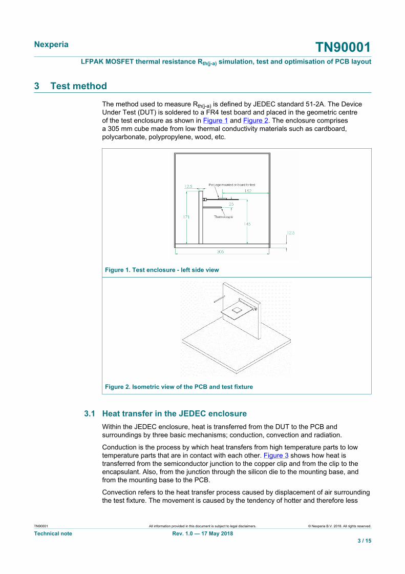
The method used to measure Rth(j-a) is defined by JEDEC standard 51-2A. The DeviceUnder Test (DUT) is soldered to a FR4 test board and placed in the geometric centreof the test enclosure as shown in Figure 1 and Figure 2. The enclosure comprisesa 305 mm cube made from low thermal conductivity materials such as cardboard,polycarbonate, polypropylene, wood, etc.
Figure 1. Test enclosure - left side view
Figure 2. Isometric view of the PCB and test fixture
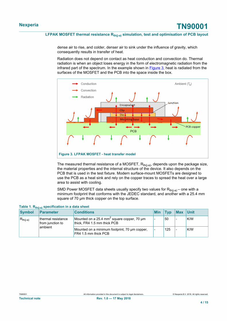
3.1 Heat transfer in the JEDEC enclosureWithin the JEDEC enclosure, heat is transferred from the DUT to the PCB andsurroundings by three basic mechanisms; conduction, convection and radiation.
Conduction is the process by which heat transfers from high temperature parts to lowtemperature parts that are in contact with each other. Figure 3 shows how heat istransferred from the semiconductor junction to the copper clip and from the clip to theencapsulant. Also, from the junction through the silicon die to the mounting base, andfrom the mounting base to the PCB.
Convection refers to the heat transfer process caused by displacement of air surroundingthe test fixture. The movement is caused by the tendency of hotter and therefore less
Nexperia TN90001LFPAK MOSFET thermal resistance Rth(j-a) simulation, test and optimisation of PCB layout
TN90001 All information provided in this document is subject to legal disclaimers. © Nexperia B.V. 2018. All rights reserved.
Technical note Rev. 1.0 — 17 May 20184 / 15
dense air to rise, and colder, denser air to sink under the influence of gravity, whichconsequently results in transfer of heat.
Radiation does not depend on contact as heat conduction and convection do. Thermalradiation is when an object loses energy in the form of electromagnetic radiation from theinfrared part of the spectrum. In the example shown in Figure 3, heat is radiated from thesurfaces of the MOSFET and the PCB into the space inside the box.
Figure 3. LFPAK MOSFET - heat transfer model
The measured thermal resistance of a MOSFET, Rth(j-a), depends upon the package size,the material properties and the internal structure of the device. It also depends on thePCB that is used in the test fixture. Modern surface-mount MOSFETs are designed touse the PCB as a heat sink and rely on the copper traces to spread the heat over a largearea to assist with cooling.
SMD Power MOSFET data sheets usually specify two values for Rth(j-a) – one with aminimum footprint that conforms with the JEDEC standard, and another with a 25.4 mmsquare of 70 µm thick copper on the top surface.
Table 1. Rth(j-a) specification in a data sheetSymbol Parameter Conditions Min Typ Max Unit
Mounted on a 25.4 mm2 square copper, 70 μmthick, FR4 1.5 mm thick PCB
- 50 - K/WRth(j-a) thermal resistancefrom junction toambient
Mounted on a minimum footprint, 70 μm copper,FR4 1.5 mm thick PCB
- 125 - K/W
Nexperia TN90001LFPAK MOSFET thermal resistance Rth(j-a) simulation, test and optimisation of PCB layout
TN90001 All information provided in this document is subject to legal disclaimers. © Nexperia B.V. 2018. All rights reserved.
Technical note Rev. 1.0 — 17 May 20185 / 15
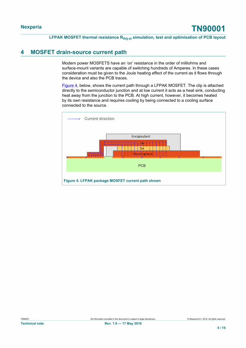
4 MOSFET drain-source current path
Modern power MOSFETS have an ‘on’ resistance in the order of milliohms andsurface-mount variants are capable of switching hundreds of Amperes. In these casesconsideration must be given to the Joule heating effect of the current as it flows throughthe device and also the PCB traces.
Figure 4, below, shows the current path through a LFPAK MOSFET. The clip is attacheddirectly to the semiconductor junction and at low current it acts as a heat sink, conductingheat away from the junction to the PCB. At high current, however, it becomes heatedby its own resistance and requires cooling by being connected to a cooling surfaceconnected to the source.
Figure 4. LFPAK package MOSFET current path shown
Nexperia TN90001LFPAK MOSFET thermal resistance Rth(j-a) simulation, test and optimisation of PCB layout
TN90001 All information provided in this document is subject to legal disclaimers. © Nexperia B.V. 2018. All rights reserved.
Technical note Rev. 1.0 — 17 May 20186 / 15
5 PCB trace width calculations
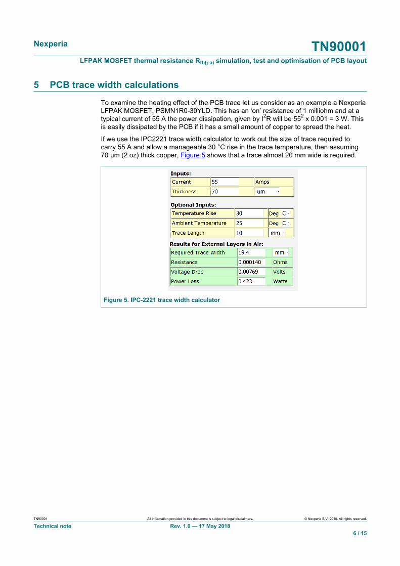
To examine the heating effect of the PCB trace let us consider as an example a NexperiaLFPAK MOSFET, PSMN1R0-30YLD. This has an ‘on’ resistance of 1 milliohm and at atypical current of 55 A the power dissipation, given by I2R will be 552 x 0.001 = 3 W. Thisis easily dissipated by the PCB if it has a small amount of copper to spread the heat.
If we use the IPC2221 trace width calculator to work out the size of trace required tocarry 55 A and allow a manageable 30 °C rise in the trace temperature, then assuming70 µm (2 oz) thick copper, Figure 5 shows that a trace almost 20 mm wide is required.
Figure 5. IPC-2221 trace width calculator
Nexperia TN90001LFPAK MOSFET thermal resistance Rth(j-a) simulation, test and optimisation of PCB layout
TN90001 All information provided in this document is subject to legal disclaimers. © Nexperia B.V. 2018. All rights reserved.
Technical note Rev. 1.0 — 17 May 20187 / 15
6 Board layout optimisation
A number of thermal simulations have been carried out using a PSMN1R0-30YLD as anexample to find the optimum PCB layout that extracts the maximum amount of heat fromthe device and therefore gives the lowest possible value for Rth(j-a). All the simulationswere on a 25.4 mm square of 70 µm thick copper. The MOSFET was fully turned on witha constant current that produced 3 W loss in the device.
The investigation examined different positions of the MOSFET within the copper square.It also considered allocating different percentages of the copper square to the sourceand drain. Finally, it examined the heating effect of trace width on the temperature of theMOSFET and the consequences for Rth(j-a) measurement.
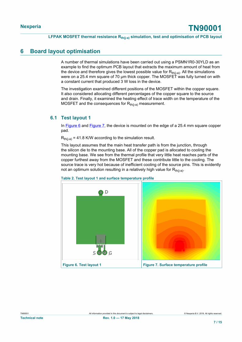
6.1 Test layout 1In Figure 6 and Figure 7, the device is mounted on the edge of a 25.4 mm square copperpad.
Rth(j-a) = 41.8 K/W according to the simulation result.
This layout assumes that the main heat transfer path is from the junction, throughthe silicon die to the mounting base. All of the copper pad is allocated to cooling themounting base. We see from the thermal profile that very little heat reaches parts of thecopper furthest away from the MOSFET and these contribute little to the cooling. Thesource trace is very hot because of inefficient cooling of the source pins. This is evidentlynot an optimum solution resulting in a relatively high value for Rth(j-a).
Table 2. Test layout 1 and surface temperature profile
Figure 6. Test layout 1 Figure 7. Surface temperature profile
Nexperia TN90001LFPAK MOSFET thermal resistance Rth(j-a) simulation, test and optimisation of PCB layout
TN90001 All information provided in this document is subject to legal disclaimers. © Nexperia B.V. 2018. All rights reserved.
Technical note Rev. 1.0 — 17 May 20188 / 15
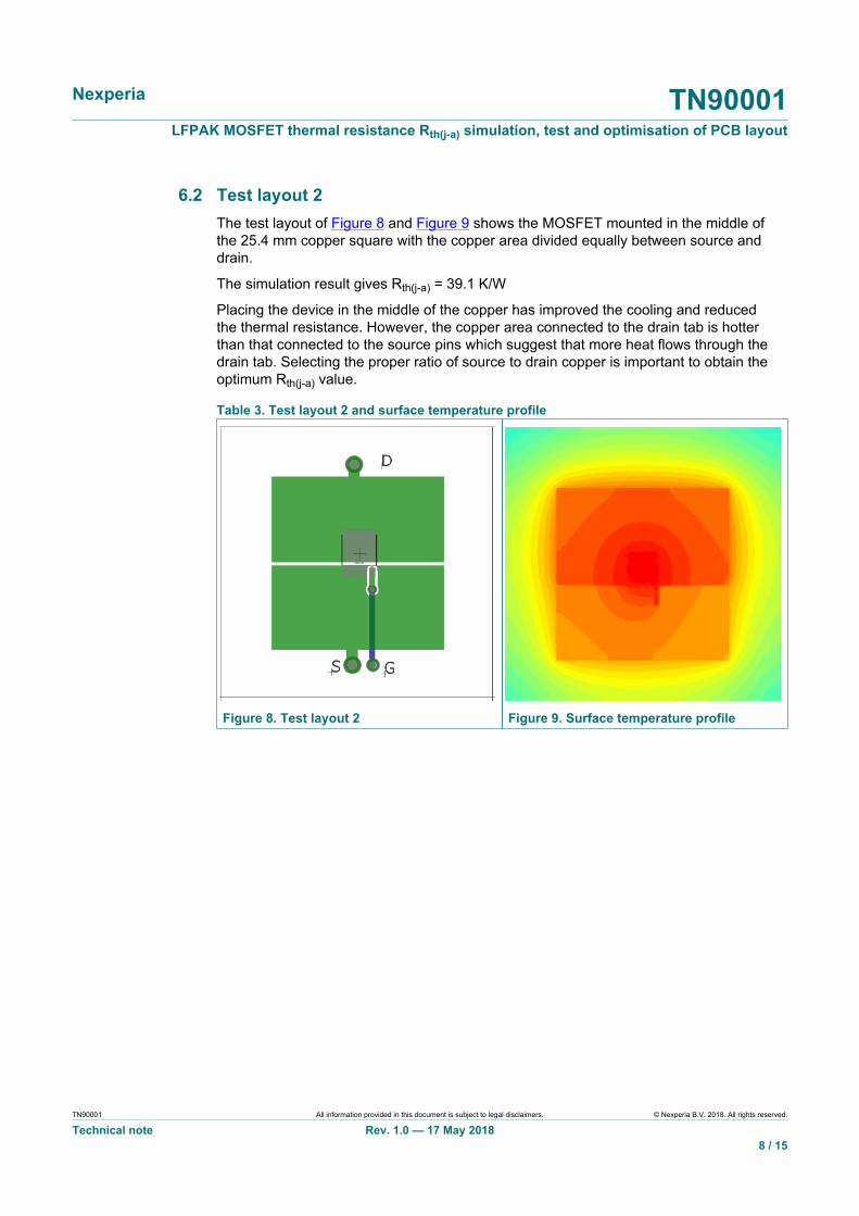
6.2 Test layout 2The test layout of Figure 8 and Figure 9 shows the MOSFET mounted in the middle ofthe 25.4 mm copper square with the copper area divided equally between source anddrain.
The simulation result gives Rth(j-a) = 39.1 K/W
Placing the device in the middle of the copper has improved the cooling and reducedthe thermal resistance. However, the copper area connected to the drain tab is hotterthan that connected to the source pins which suggest that more heat flows through thedrain tab. Selecting the proper ratio of source to drain copper is important to obtain theoptimum Rth(j-a) value.
Table 3. Test layout 2 and surface temperature profile
Figure 8. Test layout 2 Figure 9. Surface temperature profile
Nexperia TN90001LFPAK MOSFET thermal resistance Rth(j-a) simulation, test and optimisation of PCB layout
TN90001 All information provided in this document is subject to legal disclaimers. © Nexperia B.V. 2018. All rights reserved.
Technical note Rev. 1.0 — 17 May 20189 / 15
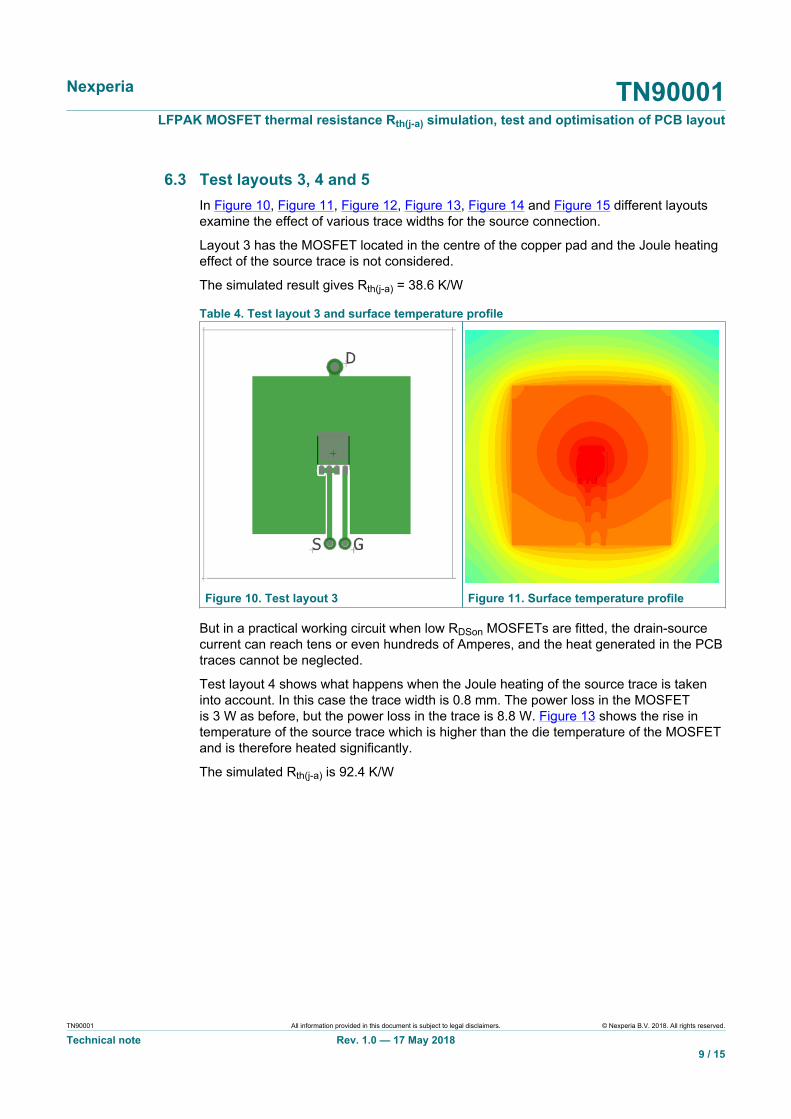
6.3 Test layouts 3, 4 and 5In Figure 10, Figure 11, Figure 12, Figure 13, Figure 14 and Figure 15 different layoutsexamine the effect of various trace widths for the source connection.
Layout 3 has the MOSFET located in the centre of the copper pad and the Joule heatingeffect of the source trace is not considered.
The simulated result gives Rth(j-a) = 38.6 K/W
Table 4. Test layout 3 and surface temperature profile
Figure 10. Test layout 3 Figure 11. Surface temperature profile
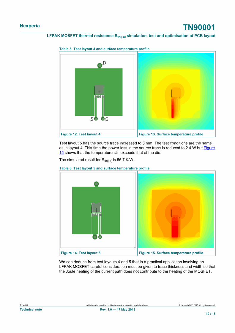
But in a practical working circuit when low RDSon MOSFETs are fitted, the drain-sourcecurrent can reach tens or even hundreds of Amperes, and the heat generated in the PCBtraces cannot be neglected.
Test layout 4 shows what happens when the Joule heating of the source trace is takeninto account. In this case the trace width is 0.8 mm. The power loss in the MOSFETis 3 W as before, but the power loss in the trace is 8.8 W. Figure 13 shows the rise intemperature of the source trace which is higher than the die temperature of the MOSFETand is therefore heated significantly.
The simulated Rth(j-a) is 92.4 K/W
Nexperia TN90001LFPAK MOSFET thermal resistance Rth(j-a) simulation, test and optimisation of PCB layout
TN90001 All information provided in this document is subject to legal disclaimers. © Nexperia B.V. 2018. All rights reserved.
Technical note Rev. 1.0 — 17 May 201810 / 15
Table 5. Test layout 4 and surface temperature profile
Figure 12. Test layout 4 Figure 13. Surface temperature profile
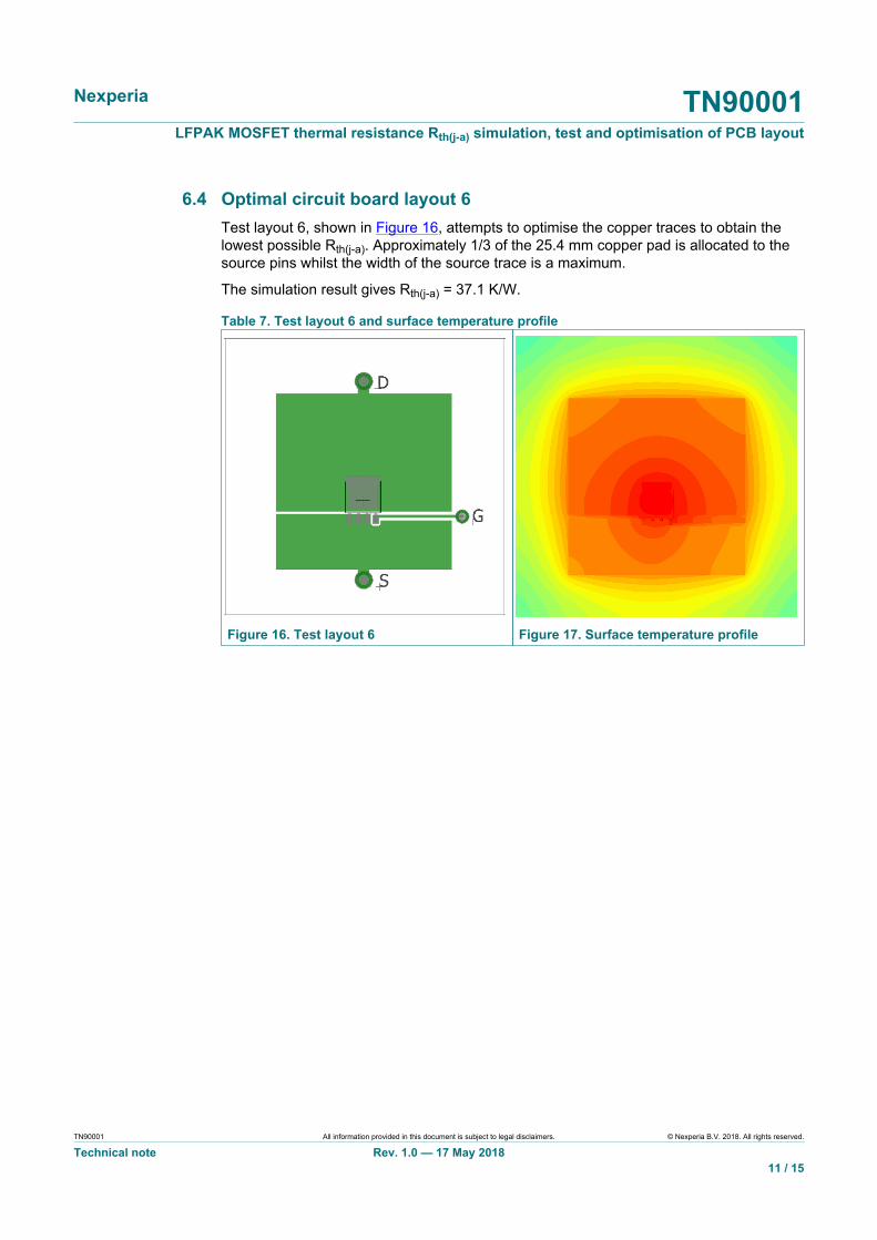
Test layout 5 has the source trace increased to 3 mm. The test conditions are the sameas in layout 4. This time the power loss in the source trace is reduced to 2.4 W but Figure15 shows that the temperature still exceeds that of the die.
The simulated result for Rth(j-a) is 56.7 K/W.
Table 6. Test layout 5 and surface temperature profile
Figure 14. Test layout 5 Figure 15. Surface temperature profile
We can deduce from test layouts 4 and 5 that in a practical application involving anLFPAK MOSFET careful consideration must be given to trace thickness and width so thatthe Joule heating of the current path does not contribute to the heating of the MOSFET.
Nexperia TN90001LFPAK MOSFET thermal resistance Rth(j-a) simulation, test and optimisation of PCB layout
TN90001 All information provided in this document is subject to legal disclaimers. © Nexperia B.V. 2018. All rights reserved.
Technical note Rev. 1.0 — 17 May 201811 / 15
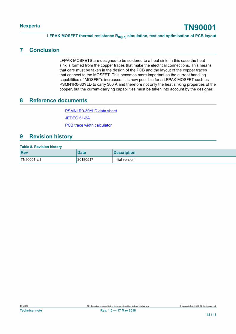
6.4 Optimal circuit board layout 6Test layout 6, shown in Figure 16, attempts to optimise the copper traces to obtain thelowest possible Rth(j-a). Approximately 1/3 of the 25.4 mm copper pad is allocated to thesource pins whilst the width of the source trace is a maximum.
The simulation result gives Rth(j-a) = 37.1 K/W.
Table 7. Test layout 6 and surface temperature profile
Figure 16. Test layout 6 Figure 17. Surface temperature profile
Nexperia TN90001LFPAK MOSFET thermal resistance Rth(j-a) simulation, test and optimisation of PCB layout
TN90001 All information provided in this document is subject to legal disclaimers. © Nexperia B.V. 2018. All rights reserved.
Technical note Rev. 1.0 — 17 May 201812 / 15
7 Conclusion
LFPAK MOSFETS are designed to be soldered to a heat sink. In this case the heatsink is formed from the copper traces that make the electrical connections. This meansthat care must be taken in the design of the PCB and the layout of the copper tracesthat connect to the MOSFET. This becomes more important as the current handlingcapabilities of MOSFETs increases. It is now possible for a LFPAK MOSFET such asPSMN1R0-30YLD to carry 300 A and therefore not only the heat sinking properties of thecopper, but the current-carrying capabilities must be taken into account by the designer.
8 Reference documents
PSMN1R0-30YLD data sheet
JEDEC 51-2A
PCB trace width calculator
9 Revision historyTable 8. Revision historyRev Date DescriptionTN90001 v.1 20180517 Initial version
Nexperia TN90001LFPAK MOSFET thermal resistance Rth(j-a) simulation, test and optimisation of PCB layout
TN90001 All information provided in this document is subject to legal disclaimers. © Nexperia B.V. 2018. All rights reserved.
Technical note Rev. 1.0 — 17 May 201813 / 15
10 Legal information
10.1 DefinitionsDraft — The document is a draft version only. The content is still underinternal review and subject to formal approval, which may result inmodifications or additions. Nexperia does not give any representations orwarranties as to the accuracy or completeness of information included hereinand shall have no liability for the consequences of use of such information.
10.2 DisclaimersLimited warranty and liability — Information in this document is believedto be accurate and reliable. However, Nexperia does not give anyrepresentations or warranties, expressed or implied, as to the accuracyor completeness of such information and shall have no liability for theconsequences of use of such information. Nexperia takes no responsibilityfor the content in this document if provided by an information source outsideof Nexperia. In no event shall Nexperia be liable for any indirect, incidental,punitive, special or consequential damages (including - without limitation -lost profits, lost savings, business interruption, costs related to the removalor replacement of any products or rework charges) whether or not suchdamages are based on tort (including negligence), warranty, breach ofcontract or any other legal theory. Notwithstanding any damages thatcustomer might incur for any reason whatsoever, Nexperia's aggregate andcumulative liability towards customer for the products described herein shallbe limited in accordance with the Terms and conditions of commercial sale ofNexperia.
Right to make changes — Nexperia reserves the right to make changesto information published in this document, including without limitationspecifications and product descriptions, at any time and without notice. Thisdocument supersedes and replaces all information supplied prior to thepublication hereof.
Suitability for use — Nexperia products are not designed, authorized orwarranted to be suitable for use in life support, life-critical or safety-criticalsystems or equipment, nor in applications where failure or malfunctionof an Nexperia product can reasonably be expected to result in personalinjury, death or severe property or environmental damage. Nexperia and itssuppliers accept no liability for inclusion and/or use of Nexperia products insuch equipment or applications and therefore such inclusion and/or use is atthe customer’s own risk.
Applications — Applications that are described herein for any of theseproducts are for illustrative purposes only. Nexperia makes no representationor warranty that such applications will be suitable for the specified usewithout further testing or modification. Customers are responsible for thedesign and operation of their applications and products using Nexperiaproducts, and Nexperia accepts no liability for any assistance withapplications or customer product design. It is customer’s sole responsibilityto determine whether the Nexperia product is suitable and fit for thecustomer’s applications and products planned, as well as for the plannedapplication and use of customer’s third party customer(s). Customers shouldprovide appropriate design and operating safeguards to minimize the risksassociated with their applications and products. Nexperia does not acceptany liability related to any default, damage, costs or problem which is basedon any weakness or default in the customer’s applications or products, or
the application or use by customer’s third party customer(s). Customer isresponsible for doing all necessary testing for the customer’s applicationsand products using Nexperia products in order to avoid a default of theapplications and the products or of the application or use by customer’s thirdparty customer(s). Nexperia does not accept any liability in this respect.
Limiting values — Stress above one or more limiting values (as defined inthe Absolute Maximum Ratings System of IEC 60134) will cause permanentdamage to the device. Limiting values are stress ratings only and (proper)operation of the device at these or any other conditions above thosegiven in the Recommended operating conditions section (if present) or theCharacteristics sections of this document is not warranted. Constant orrepeated exposure to limiting values will permanently and irreversibly affectthe quality and reliability of the device.
Terms and conditions of commercial sale — Nexperia products aresold subject to the general terms and conditions of commercial sale, aspublished at http://www.nexperia.com/profile/terms, unless otherwise agreedin a valid written individual agreement. In case an individual agreement isconcluded only the terms and conditions of the respective agreement shallapply. Nexperia hereby expressly objects to applying the customer’s generalterms and conditions with regard to the purchase of Nexperia products bycustomer.
No offer to sell or license — Nothing in this document may be interpretedor construed as an offer to sell products that is open for acceptance orthe grant, conveyance or implication of any license under any copyrights,patents or other industrial or intellectual property rights.
Export control — This document as well as the item(s) described hereinmay be subject to export control regulations. Export might require a priorauthorization from competent authorities.
Non-automotive qualified products — Unless this data sheet expresslystates that this specific Nexperia product is automotive qualified, theproduct is not suitable for automotive use. It is neither qualified nor tested inaccordance with automotive testing or application requirements. Nexperiaaccepts no liability for inclusion and/or use of non-automotive qualifiedproducts in automotive equipment or applications. In the event that customeruses the product for design-in and use in automotive applications toautomotive specifications and standards, customer (a) shall use the productwithout Nexperia's warranty of the product for such automotive applications,use and specifications, and (b) whenever customer uses the product forautomotive applications beyond Nexperia's specifications such use shall besolely at customer’s own risk, and (c) customer fully indemnifies Nexperiafor any liability, damages or failed product claims resulting from customerdesign and use of the product for automotive applications beyond Nexperia'sstandard warranty and Nexperia's product specifications.
Translations — A non-English (translated) version of a document is forreference only. The English version shall prevail in case of any discrepancybetween the translated and English versions.
10.3 TrademarksNotice: All referenced brands, product names, service names andtrademarks are the property of their respective owners.

Nexperia TN90001LFPAK MOSFET thermal resistance Rth(j-a) simulation, test and optimisation of PCB layout
TN90001 All information provided in this document is subject to legal disclaimers. © Nexperia B.V. 2018. All rights reserved.
Technical note Rev. 1.0 — 17 May 201814 / 15
TablesTab. 1. Rth(j-a) specification in a data sheet .................4Tab. 2. Test layout 1 and surface temperature
profile .................................................................7Tab. 3. Test layout 2 and surface temperature
profile .................................................................8Tab. 4. Test layout 3 and surface temperature
profile .................................................................9
Tab. 5. Test layout 4 and surface temperatureprofile ...............................................................10
Tab. 6. Test layout 5 and surface temperatureprofile ...............................................................10
Tab. 7. Test layout 6 and surface temperatureprofile ...............................................................11
Tab. 8. Revision history ...............................................12
FiguresFig. 1. Test enclosure - left side view .......................... 3Fig. 2. Isometric view of the PCB and test fixture .........3Fig. 3. LFPAK MOSFET - heat transfer model .............4Fig. 4. LFPAK package MOSFET current path
shown ................................................................ 5Fig. 5. IPC-2221 trace width calculator ........................ 6Fig. 6. Test layout 1 ..................................................... 7Fig. 7. Surface temperature profile ...............................7Fig. 8. Test layout 2 ..................................................... 8
Fig. 9. Surface temperature profile ...............................8Fig. 10. Test layout 3 ..................................................... 9Fig. 11. Surface temperature profile ...............................9Fig. 12. Test layout 4 ................................................... 10Fig. 13. Surface temperature profile .............................10Fig. 14. Test layout 5 ................................................... 10Fig. 15. Surface temperature profile .............................10Fig. 16. Test layout 6 ................................................... 11Fig. 17. Surface temperature profile .............................11
Nexperia TN90001LFPAK MOSFET thermal resistance Rth(j-a) simulation, test and optimisation of PCB layout
Please be aware that important notices concerning this document and the product(s)described herein, have been included in section 'Legal information'.
© Nexperia B.V. 2018. All rights reserved.For more information, please visit: http://www.nexperia.comFor sales office addresses, please send an email to: [email protected]
Date of release: 17 May 2018Document identifier: TN90001
Contents1 Introduction ......................................................... 22 Definition of Thermal Resistance Rth(j-a) .........23 Test method .........................................................33.1 Heat transfer in the JEDEC enclosure ...............34 MOSFET drain-source current path .................. 55 PCB trace width calculations .............................66 Board layout optimisation ..................................76.1 Test layout 1 ......................................................76.2 Test layout 2 ......................................................86.3 Test layouts 3, 4 and 5 ..................................... 96.4 Optimal circuit board layout 6 ..........................117 Conclusion .........................................................128 Reference documents .......................................129 Revision history ................................................ 1210 Legal information ..............................................13