
Multi-Scale Model of the RF Diode Sputter Deposition … · is capable of predicting the thin-film...
16
1 Multi-Scale Model of the RF Diode Sputter Deposition of GMR Thin Films S. Ghosal, R.L. Kosut, J.L. Ebert, A. Kozak, T.E. Abrahamson SC Solutions, Santa Clara, CA 95054 E-mail [email protected] W. Zou, X.W. Zhou, J.F. Groves, Y.G. Yang, H.N.G. Wadley University of Virginia, Charlottesville, VA 22903 D. Brownell, D. Wang Nonvolatile Electronics, Inc., Eden Prairie, MN 55344 1. Introduction Radio frequency (RF) diode sputtering deposition is a widely used process for depositing thin films and multilayers [1-3]. The development, computational implementation, and integration of the appropriate physical models for RF diode sputtering, calibrated and refined using appropriate experimental results are believed to promise a reduction of the time consuming and costly trial-and-error approach used to design, operate, and control deposition systems used for the reliable fabrication of high-quality thin metal films. To meet these objectives, a multiscale model based on the primary physical phenomena - gas flow, plasma discharge, sputtering and atom transport has been assembled to explore the RF diode deposition of thin metal films. The resulting multiscale input-output model is capable of predicting the thin-film deposition rate, the sputtered metal atoms’ energy and angular distribution, both upon emission at the target and just prior to deposition at the substrate, and their sensitivity to deposition conditions such as power, working gas type, pressure, gas temperature, and electrode spacing. The metal atom flux incident upon the substrate is then used as an input to atom assembly models to deduce surface morphology and film structure. The deduced performance measures of the RF diode deposition process, such as wafer-scale uniformity of the film thickness and surface roughness of the film, in turn, influence device characteristics that utilize these films, e.g. the saturation magnetic field, and magnetoresistance of giant magnetoresistive multilayer [1]. ∗ ∗ Acknowledgements This work was supported by the Applied Computation and Mathematics Program at Defence Advanced Research Projects Agency (DARPA). Dr. A. Tsao was the program manager. Target Target Target Target Tray Tray Poppet value Tray cut-away Chamber inner wall Dark shield Susceptor electrode Substrate Counter weight Exhaust V rf RF-power Figure 1. Schematic of the RF diode sputter chamber. The modeling approach uses: (1) a computational fluid dynamic (CFD) finite element model to compute the velocity and pressure distribution of the working gas (argon) within a deposition chamber, (2) a one-dimensional steady- state plasma model, to determine the flux and energy of the argon ions that strike both the target and substrate, (3) results of a molecular dynamics analysis of sputtering to deduce the energy distribution, angle distribution, and sputter yield of metal atoms from the target, and (4) a Direct Simulation Monte Carlo (DSMC) model to track the propagation (and energy loss) of metal atoms through the argon working gas from the copper target to a substrate. The outputs of this sequence of models are the incident energy and angle distributions of the metal atoms at the substrate surface as functions of the working gas pressure, temperature, and the plasma power. A two dimensional, hyperthermal kinetic Monte Carlo model is then used to relate the film surface morphology and atomic scale structure to the flux parameters and therefore the conditions of the vapor deposition process. The individual models for gas flow, plasma discharge, sputtering, metal atom transport, and kinetic Monte Carlo models developed for copper are then integrated to create a detailed, steady-state, input-output, multiscale model. The menus is organized as follows. The RF diode sputtering process, experimental results, and the reactor scale models of interest for metal thin-film fabrication are briefly
Transcript of Multi-Scale Model of the RF Diode Sputter Deposition … · is capable of predicting the thin-film...

1
Multi-Scale Model of the RF Diode Sputter Deposition of GMR Thin Films
S. Ghosal, R.L. Kosut, J.L. Ebert, A. Kozak, T.E. Abrahamson SC Solutions, Santa Clara, CA 95054
E-mail [email protected]
W. Zou, X.W. Zhou, J.F. Groves, Y.G. Yang, H.N.G. WadleyUniversity of Virginia, Charlottesville, VA 22903
D. Brownell, D. WangNonvolatile Electronics, Inc., Eden Prairie, MN 55344
1. Introduction
Radio frequency (RF) diode sputtering deposition is awidely used process for depositing thin films andmultilayers [1-3]. The development, computationalimplementation, and integration of the appropriatephysical models for RF diode sputtering, calibrated andrefined using appropriate experimental results arebelieved to promise a reduction of the time consumingand costly trial-and-error approach used to design,operate, and control deposition systems used for thereliable fabrication of high-quality thin metal films. Tomeet these objectives, a multiscale model based on theprimary physical phenomena - gas flow, plasmadischarge, sputtering and atom transport has beenassembled to explore the RF diode deposition of thinmetal films. The resulting multiscale input-output modelis capable of predicting the thin-film deposition rate, thesputtered metal atoms’ energy and angular distribution,both upon emission at the target and just prior todeposition at the substrate, and their sensitivity todeposition conditions such as power, working gas type,pressure, gas temperature, and electrode spacing. Themetal atom flux incident upon the substrate is then used asan input to atom assembly models to deduce surfacemorphology and film structure. The deducedperformance measures of the RF diode depositionprocess, such as wafer-scale uniformity of the filmthickness and surface roughness of the film, in turn,influence device characteristics that utilize these films,e.g. the saturation magnetic field, and magnetoresistanceof giant magnetoresistive multilayer [1].
∗
∗ Acknowledgements
This work was supported by the Applied Computationand Mathematics Program at Defence Advanced ResearchProjects Agency (DARPA). Dr. A. Tsao was the programmanager.
Target
Target
Target
Target
Tray
TrayPoppetvalue
Tray cut-away
Chamber inner wall
Dark shield
Susceptor electrode
Substrate Counter weight
Exhaust
Vrf
RF-power
Figure 1. Schematic of the RF diode sputter chamber.
The modeling approach uses: (1) a computational fluiddynamic (CFD) finite element model to compute thevelocity and pressure distribution of the working gas (argon)within a deposition chamber, (2) a one-dimensional steady-state plasma model, to determine the flux and energy of theargon ions that strike both the target and substrate, (3)results of a molecular dynamics analysis of sputtering todeduce the energy distribution, angle distribution, andsputter yield of metal atoms from the target, and (4) a DirectSimulation Monte Carlo (DSMC) model to track thepropagation (and energy loss) of metal atoms through theargon working gas from the copper target to a substrate. Theoutputs of this sequence of models are the incident energyand angle distributions of the metal atoms at the substratesurface as functions of the working gas pressure,temperature, and the plasma power. A two dimensional,hyperthermal kinetic Monte Carlo model is then used torelate the film surface morphology and atomic scalestructure to the flux parameters and therefore the conditionsof the vapor deposition process. The individual models forgas flow, plasma discharge, sputtering, metal atomtransport, and kinetic Monte Carlo models developed forcopper are then integrated to create a detailed, steady-state,input-output, multiscale model.
The menus is organized as follows. The RF diode sputteringprocess, experimental results, and the reactor scale modelsof interest for metal thin-film fabrication are briefly
2
reviewed in Section 2. The development of model andrelevant results for the fluid flow, the plasma, the sputtering,the vapor phase atom transport, and film growth areaddressed in Sections 3, 4, 5, 6, and 7 respectively. Adetailed integrated, steady-state, input-output model for RFdiode sputtering for growing thin metal films that resultsfrom the integration of these individual models is describedin Section 8. An approximate coarse grained input-outputversion of the detailed model provides reasonablepredictions of process performance several orders-of-magnitude faster than the detailed model, and is described inthis section. The coarse grained model, when refined andvalidated with experimental data, is shown to be useful forperformance sensitivity analysis of deposition rate anduniformity with respect to input power, pressure,temperature, and electrode spacing. Sensitivity results aregiven in Section 8. Dependence of measured surfacemorphology on plasma power and background pressure wascorrectly predicted by the models. In Section 9, we showhow these sensitivity results can be used to derive set-pointcontrol tolerances for the critical thin-film layer in an actualdiode-sputtering process. Finally, Section 10 describes howdeposition uniformity was substantially improved by targetshaping, a process modification resulting directly from thesimulation studies that successfully passed all thequalification tests needed to incorporate a modification intoNVE’s regular manufacturing process.
2. The RF Diode Deposition Process
A schematic diagram of an RF diode sputter chamber isshown in Figure 1. The chamber depicted in this figurerepresents the essential elements of a Perkins Elmer 2400sputtering system at Nonvolatile Electronics (NVE) whereall the experiments were performed. Copper was chosenfor this study because it is commonly used as theconducting layer in several giant magnetoresistiveapplications [1-3]. The copper target for sputtering wasmounted at the top of the chamber while the wafer onwhich the thin film is deposited is mounted at the bottom.Although four targets are present in the chamber duringmultilayer processing, only the target directly above thesubstrate is active during the deposition of a layer. Argongas at low pressure (20-50 mTorr) flows continuouslythrough the chamber. An RF plasma discharge isgenerated and maintained between the target electrodeand the wafer (substrate) electrode by means of a powersupply and RF matching network. Argon ions formed inthe plasma bombard the copper target and result in copperatom ejection, which propagate through the argon and aredeposited on the wafer substrate.
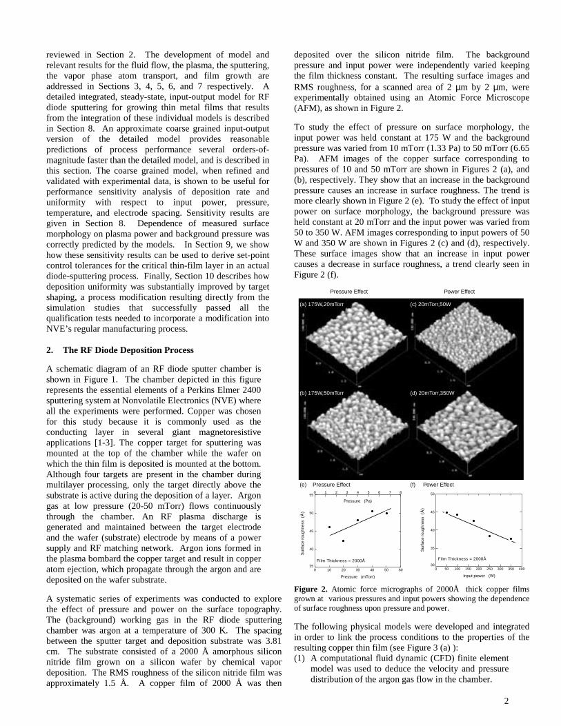
A systematic series of experiments was conducted to explorethe effect of pressure and power on the surface topography.The (background) working gas in the RF diode sputteringchamber was argon at a temperature of 300 K. The spacingbetween the sputter target and deposition substrate was 3.81cm. The substrate consisted of a 2000 Å amorphous siliconnitride film grown on a silicon wafer by chemical vapordeposition. The RMS roughness of the silicon nitride film wasapproximately 1.5 Å. A copper film of 2000 Å was then
deposited over the silicon nitride film. The backgroundpressure and input power were independently varied keepingthe film thickness constant. The resulting surface images andRMS roughness, for a scanned area of 2 µm by 2 µm, wereexperimentally obtained using an Atomic Force Microscope(AFM), as shown in Figure 2.
To study the effect of pressure on surface morphology, theinput power was held constant at 175 W and the backgroundpressure was varied from 10 mTorr (1.33 Pa) to 50 mTorr (6.65Pa). AFM images of the copper surface corresponding topressures of 10 and 50 mTorr are shown in Figures 2 (a), and(b), respectively. They show that an increase in the backgroundpressure causes an increase in surface roughness. The trend ismore clearly shown in Figure 2 (e). To study the effect of inputpower on surface morphology, the background pressure washeld constant at 20 mTorr and the input power was varied from50 to 350 W. AFM images corresponding to input powers of 50W and 350 W are shown in Figures 2 (c) and (d), respectively.These surface images show that an increase in input powercauses a decrease in surface roughness, a trend clearly seen inFigure 2 (f).
Sur
face
rou
ghne
ss (
)
Prediction
Pressure (mTorr)
Pressure (Pa)
0 10 3020 40 50 60
0 1 2 3 4 5 6 7 8
35
40
45
50
55
Film Thickness = 2000Å
Input power (W)
30
35
40
45
50
0 50 150100 200 250 300 350 400
Sur
face
rou
ghne
ss (
)
Film Thickness = 2000Å
Pressure Effect Power Effect
(a) 175W,20mTorr
(b) 175W,50mTorr
(e) Pressure Effect
(c) 20mTorr,50W
(d) 20mTorr,350W
(f) Power Effect
Figure 2. Atomic force micrographs of 2000Å thick copper filmsgrown at various pressures and input powers showing the dependenceof surface roughness upon pressure and power.
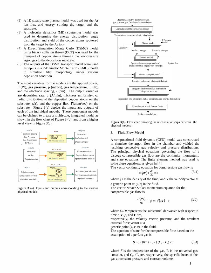
The following physical models were developed and integratedin order to link the process conditions to the properties of theresulting copper thin film (see Figure 3 (a) ):(1) A computational fluid dynamic (CFD) finite element
model was used to deduce the velocity and pressuredistribution of the argon gas flow in the chamber.
3
(2) A 1D steady-state plasma model was used for the Arion flux and energy striking the target and thesubstrate,
(3) A molecular dynamics (MD) sputtering model wasused to determine the energy distribution, angledistribution, and yield of the copper atoms sputteredfrom the target by the Ar ions.
(4) A Direct Simulation Monte Carlo (DSMC) modelusing binary collision theory (BCT) was used for thetransport of copper atoms through the low-pressureargon gas to the deposition substrate.
(5) The outputs of the DSMC transport model were usedas inputs in a 2-D kinetic Monte Carlo (KMC) modelto simulate film morphology under variousdeposition condition.
The input variables for the models are the applied power,P (W), gas pressure, p (mTorr), gas temperature, T (K),and the electrode spacing, l (cm). The output variablesare deposition rate, d (Å/min), thickness uniformity, σ,radial distribution of the deposited copper atoms on thesubstrate, φ(r), and the copper flux, ΓΓΓΓ(atom/sec) on thesubstrate. Figure 3(a) depicts the inputs and outputs ofeach of the individual models. These component modelscan be chained to create a multiscale, integrated model asshown in the flow chart of Figure 3 (b), and from a higherlevel view in Figure 3(c).
Ar+
plasmatarget
RF Plasma Model1
Outputs
Ion energy
Sheath voltages
Ion flux (current)Gas PressureGas Temperature
RF Power
Electrode Spacing
I nputs
targetgas
substrate
DSMC Model (BCT)
OutputsInputs
Atom energy at substrate
Interaction potentials
Emission energy
Emitted atom direction Atom trajectory at substrate
Deposition efficiency
Cu Ar
target
MD Sputter Model
Outputs
Sputtered atom energyIon flux
I nputs
Ion energy
Sputtered atom direction
Sputtered atom flux
Target properties
Ar+Cu
Figure 3 (a). Inputs and outputs corresponding to the variousphysical models.
Chamber geometry, gas temperature, gas pressure, gas flow boundary conditions
Temperature, pressure, velocity distributions
RF power
Geometry Ion flux, energy Electrode voltages
Sputtered atom energy, angle of Sputter flux emission from a single point on target
Location and energy of deposited atom
Deposition rate, efficiency, radial uniformity, and energy distribution
Surface morphology
Computational fluid dynamics model
Plasma model
Sputter model
DSMC transport model
Integration for continuous distributionof sputter sources
Hyperthermal kinetic Monte Carlo
Figure 3(b). Flow chart showing the inter-relationships between thephysical models.
3. Fluid Flow Model
A computational fluid dynamic (CFD) model was constructedto simulate the argon flow in the chamber and yielded theresulting convective gas velocity and pressure distributions.The principal physical equations governing the flow of aviscous compressible gas flow are the continuity, momentum,and state equations. The finite element method was used tosolve these equations. as given in [4].The vector continuity equation for compressible gas flow is ( ) 0=
∂ρ∂+ρ⋅∇t
V (3.1)
where ρ is the density of the fluid, and V the velocity vector ata generic point (x, y, z) in the fluid.The vector Navier-Stokes momentum equation for thecompressible gas flow is
( ) ( ) FVV +µ∇=∇+ρ 2pDt
D (3.2)
where D/Dt represents the substantial derivative with respect totime t; V, p, and F are,respectively, the velocity vector, pressure, and the resultantexternal force vector at ageneric point (x, y, z) in the fluid.The equation of state for the compressible flow based on theassumption of a perfect gas is
ρ = p/ (RT ) = p/ [ (Cp – Cv) T ] (3.3)
where T is the temperature of the gas, R is the universal gasconstant, and Cp, Cv are, respectively, the specific heats of thegas at constant pressure and constant volume.
4
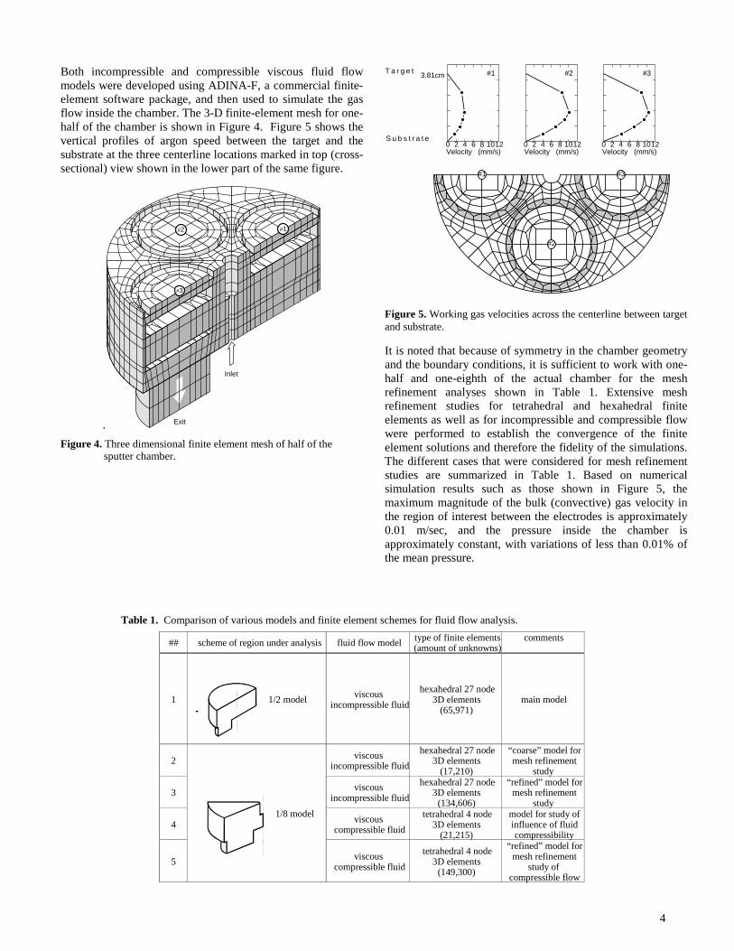
Both incompressible and compressible viscous fluid flowmodels were developed using ADINA-F, a commercial finite-element software package, and then used to simulate the gasflow inside the chamber. The 3-D finite-element mesh for one-half of the chamber is shown in Figure 4. Figure 5 shows thevertical profiles of argon speed between the target and thesubstrate at the three centerline locations marked in top (cross-sectional) view shown in the lower part of the same figure.
. Exit
Inlet
#1#2
#3
Figure 4. Three dimensional finite element mesh of half of thesputter chamber.
0 2 4 6 8 1012Velocity (mm/s)
0 2 4 6 8 1012Velocity (mm/s)
0 2 4 6 8 1012Velocity (mm/s)
#1
#2
#3#1
#2 #3T a r g e t
S u b s t r a t e
3.81cm
Figure 5. Working gas velocities across the centerline between target and substrate.
It is noted that because of symmetry in the chamber geometryand the boundary conditions, it is sufficient to work with one-half and one-eighth of the actual chamber for the meshrefinement analyses shown in Table 1. Extensive meshrefinement studies for tetrahedral and hexahedral finiteelements as well as for incompressible and compressible flowwere performed to establish the convergence of the finiteelement solutions and therefore the fidelity of the simulations.The different cases that were considered for mesh refinementstudies are summarized in Table 1. Based on numericalsimulation results such as those shown in Figure 5, themaximum magnitude of the bulk (convective) gas velocity inthe region of interest between the electrodes is approximately0.01 m/sec, and the pressure inside the chamber isapproximately constant, with variations of less than 0.01% ofthe mean pressure.
Table 1. Comparison of various models and finite element schemes for fluid flow analysis.
## scheme of region under analysis fluid flow model type of finite elements(amount of unknowns)
comments
1 1/2 model viscousincompressible fluid
hexahedral 27 node3D elements
(65,971)main model
2 viscousincompressible fluid
hexahedral 27 node3D elements
(17,210)
“coarse” model formesh refinement
study
3 viscousincompressible fluid
hexahedral 27 node3D elements
(134,606)
“refined” model formesh refinement
study
4 viscouscompressible fluid
tetrahedral 4 node3D elements
(21,215)
model for study ofinfluence of fluidcompressibility
5
1/8 model
viscouscompressible fluid
tetrahedral 4 node3D elements
(149,300)
“refined” model formesh refinement
study ofcompressible flow
5
4. Plasma Model
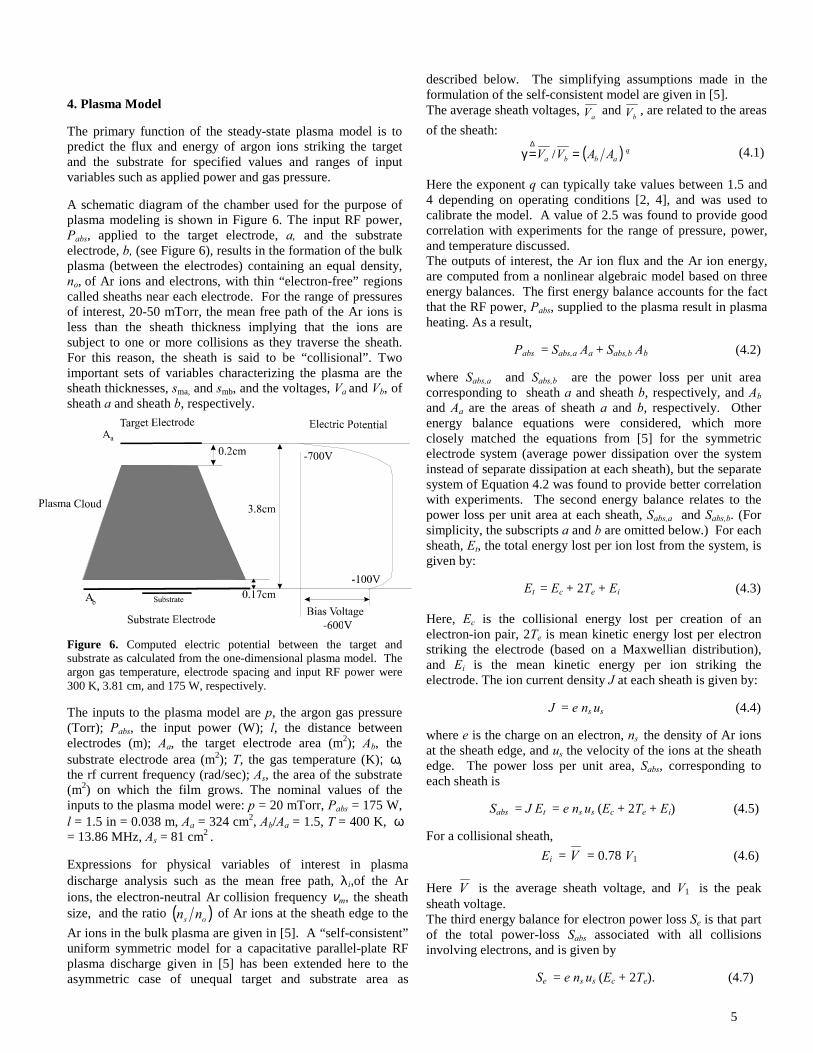
The primary function of the steady-state plasma model is topredict the flux and energy of argon ions striking the targetand the substrate for specified values and ranges of inputvariables such as applied power and gas pressure.
A schematic diagram of the chamber used for the purpose ofplasma modeling is shown in Figure 6. The input RF power,Pabs, applied to the target electrode, a, and the substrateelectrode, b, (see Figure 6), results in the formation of the bulkplasma (between the electrodes) containing an equal density,no, of Ar ions and electrons, with thin “electron-free” regionscalled sheaths near each electrode. For the range of pressuresof interest, 20-50 mTorr, the mean free path of the Ar ions isless than the sheath thickness implying that the ions aresubject to one or more collisions as they traverse the sheath.For this reason, the sheath is said to be “collisional”. Twoimportant sets of variables characterizing the plasma are thesheath thicknesses, sma, and smb, and the voltages, Va and Vb, ofsheath a and sheath b, respectively.
Figure 6. Computed electric potential between the target andsubstrate as calculated from the one-dimensional plasma model. Theargon gas temperature, electrode spacing and input RF power were300 K, 3.81 cm, and 175 W, respectively.
The inputs to the plasma model are p, the argon gas pressure(Torr); Pabs, the input power (W); l, the distance betweenelectrodes (m); Aa, the target electrode area (m2); Ab, thesubstrate electrode area (m2); T, the gas temperature (K); ω,the rf current frequency (rad/sec); As, the area of the substrate(m2) on which the film grows. The nominal values of theinputs to the plasma model were: p = 20 mTorr, Pabs = 175 W,l = 1.5 in = 0.038 m, Aa = 324 cm2, Ab/Aa = 1.5, T = 400 K, ω= 13.86 MHz, As = 81 cm2 .
Expressions for physical variables of interest in plasmadischarge analysis such as the mean free path, λi,of the Arions, the electron-neutral Ar collision frequency νm, the sheathsize, and the ratio ( )os nn of Ar ions at the sheath edge to theAr ions in the bulk plasma are given in [5]. A “self-consistent”uniform symmetric model for a capacitative parallel-plate RFplasma discharge given in [5] has been extended here to theasymmetric case of unequal target and substrate area as
described below. The simplifying assumptions made in theformulation of the self-consistent model are given in [5].The average sheath voltages,
aV and bV , are related to the areas
of the sheath:
( ) qabba AAVV ==γ
∆/ (4.1)
Here the exponent q can typically take values between 1.5 and4 depending on operating conditions [2, 4], and was used tocalibrate the model. A value of 2.5 was found to provide goodcorrelation with experiments for the range of pressure, power,and temperature discussed.The outputs of interest, the Ar ion flux and the Ar ion energy,are computed from a nonlinear algebraic model based on threeenergy balances. The first energy balance accounts for the factthat the RF power, Pabs, supplied to the plasma result in plasmaheating. As a result,
Pabs = Sabs,a Aa + Sabs,b Ab (4.2)
where Sabs,a and Sabs,b are the power loss per unit areacorresponding to sheath a and sheath b, respectively, and Aband Aa are the areas of sheath a and b, respectively. Otherenergy balance equations were considered, which moreclosely matched the equations from [5] for the symmetricelectrode system (average power dissipation over the systeminstead of separate dissipation at each sheath), but the separatesystem of Equation 4.2 was found to provide better correlationwith experiments. The second energy balance relates to thepower loss per unit area at each sheath, Sabs,a and Sabs,b. (Forsimplicity, the subscripts a and b are omitted below.) For eachsheath, Et, the total energy lost per ion lost from the system, isgiven by:
Et = Ec + 2Te + Ei (4.3)
Here, Ec is the collisional energy lost per creation of anelectron-ion pair, 2Te is mean kinetic energy lost per electronstriking the electrode (based on a Maxwellian distribution),and Ei is the mean kinetic energy per ion striking theelectrode. The ion current density J at each sheath is given by:
J = e ns us (4.4)
where e is the charge on an electron, ns the density of Ar ionsat the sheath edge, and us the velocity of the ions at the sheathedge. The power loss per unit area, Sabs, corresponding toeach sheath is
Sabs = J Et = e ns us (Ec + 2Te + Ei) (4.5)
For a collisional sheath, Ei = V = 0.78 V1 (4.6)
Here V is the average sheath voltage, and V1 is the peaksheath voltage.The third energy balance for electron power loss Se is that partof the total power-loss Sabs associated with all collisionsinvolving electrons, and is given by
Se = e ns us (Ec + 2Te). (4.7)

6
Se is attributable to ohmic heating in the bulk plasma Sohm,p,ohmic heating in the sheath Sohm,s, and stochastic heating inthe sheath Sstoc,s. In terms of these quantities Se can beexpressed as follows [5]:
Se = Sohm,p/2 + Sohm,s + Sstoc,s (4.8)
Combining equations (4.5) - (4.8), we obtain for eachsheath
Sabs = (Sohm,p/2 + Sohm,s + Sstoc,s) ��
���
�
++
ec TEV
21 (4.9)
Equation (4.9) can then be used in equation (4.2), once foreach sheath. The basic parameters and variables for theplasma discharge enter equation (4.2) through thefollowing nonlinear equations for Sohm,p, Sohm,s, and Sstoc,s.The ohmic heating pohmS , in the bulk plasma in given by
dVS pohm~
, α= , (4.10)
where ( )( ) 5.02
00273.1 ems Tvnnem ωεα = (4.11)
( ) 25.011
5.01
5.01
~baba VVVVV −+= (4.12)
Here, m = mass of the electron, e = charge on the electron,
0ε = permittivity of vacuum, ns = ion density at the sheathedge, n0 = ion density in the bulk plasma, ω = RF frequency,vm = frequency of collisions between electrons and neutralAr atoms, Te = electron temperature (volts), and d =thickness of the plasma. The ohmic heating in the sheath isgiven by
( ) ( )[ ]5.01
5.01
5.01, 39.416.1235.0 VTTVsVS eemsohm ++α= (4.13)
Here α is given by (4.11).The stochastic heating in the sheath, sstocS ,
~ is given by
( ) 15.02
05.0
, 61.0~ VTemS epstoc ωε= (4.14)
Here V1 is the peak voltage across the sheath. The iterativeprocess used to solve for the sheath thicknesses and sheathvoltages, Ar ion densities, and Ar ion velocities is describedin [5]. The equations for these parameters are coupled, andcan not be solve in a closed form solution. These equationsare nearly unchanged from those proposed in [5]. Theoutput quantities of interest from the plasma model are J,the ion current, given by (4.4), and εic, the energy of the ionswhen they strike the electrode, given by
εic = 0.62 (λ i/sm) V (4.16)
Here λ i is the mean-free path of the ions. The set of non-linear equations described above constitute the steady-stateplasma model. It was solved using Xmath, part of theMATRIXx™ commercial package used for systems andcontrols simulation [6]. The plasma model was calibratedusing experimental results on NVE’s RF diode-sputteringchamber. Figure 7 shows a comparison of plasma model
predictions and experimental data for the bias voltage acrossthe electrodes, which is the magnitude of the differencebetween the two sheath voltages, as a function of pressureand input RF power, after adjusting (or calibrating) themodel (proper choice of the value of the exponent q inEquation 4.1, etc.).
Model simulation results shown in Figure 8 indicate thatincreasing the input power significantly increases the ioncurrent density (or ion flux) and ion energy. Figure 9 showsthat increasing the pressure slightly increases the ion currentdensity (or ion flux) while significantly decreasing the ionenergy. Several other useful plasma model simulationresults are documented in [5].
Background pressure (mTorr)
Background pressure (Pa)
0 10 3020 40 50 60
0 1 2 3 4 5 6 7 8
400
500
600
700
Bia
s vo
ltage
(V
)
Simulation
Experiment
Background pressure (mTorr)
Background pressure (Pa)
0 10 3020 40 50 60
0 1 2 3 4 5 6 7 8
400
500
600
700
Bia
s vo
ltage
(V
)
Simulation
Experiment
Figure 7. Experimental validation of the plasma model showingpredicted and measured bias voltages at various chamber pressuresand RF powers. The argon gas temperature and electrode spacingwere 300 K and 3.81 cm, respectively.

7
Input power (W)
0
100
200
300
400
500
600
Ar
ion
ene
rgy
(eV
)
0 50 150100 200 250 300 350 400
at target
at substrate
+
(b) Ion Energy
Input power (W)
0
2
4
6
8
10
12
0.00
1.25
2.50
3.75
5.00
6.25
7.50 x 10¹⁹
Ar
ion
curr
ent d
ensi
ty
(A /
m2)
Ar
ion
flux
(A
tom
s / m
2 / s
ec)
0 50 150100 200 250 300 350 400
at target
at substrate+ +
(a) Ion Flux
Figure 8. Plasma model results showing the effect of power onAr+ ion current density and Ar+ ion energy at the target and thesubstrate.
Background pressure (mTorr)
Background pressure (Pa)
0 10 3020 40 50 60
0 1 2 3 4 5 6 7 8
0
2
4
6
8
10
Ar
ion
curr
ent d
ensi
ty
(A /
m2)
at target
at substrate
0.00
1.25
2.50
3.75
5.00
6.25 x 10¹⁹
Ar
ion
flux
(A
tom
s / m
2 / s
ec)
+ +
(a) Ion Flux
Background pressure (mTorr)
Background pressure (Pa)
0 10 3020 40 50 60
0 1 2 3 4 5 6 7 8
600
500
800
700
400
300
200
100
0
Ar
ion
ener
gy
(eV
)
at target
at substrate
+
(b) Ion Energy
Figure 9. Plasma model results showing the effort of pressure
on Ar + ions current density and on energy at both the target andthe substrate.
5. Sputter Model
When energetic Ar ions bombard a copper target, some ofthe atoms are sputtered (ejected) from the copper surface.To analyze this process, the Ar ions were modeled using auniversal potential [15]. An embedded atom potentialmethod was used to model the interaction forces betweenthe copper atoms in a (111) flat single crystal target. Thesputter yield, Y, and the distribution of the energy, εcu, andangle, αcu, of the sputtered copper atoms as a function ofthe energy, εi, and incident angle, θ, of the Ar ions strikingthe target were computed using a molecular dynamicssputter model that simulates Ar impacts with the coppertarget [7]. The model also takes into account the effect ofthe texture of the target surface. The inputs to the sputtermodel are the ion current density Ji, and the mean ionimpact energy εic, which are the outputs of the plasmadischarge model.
The ion energy, ε, was fitted to a Rayleigh distribution [6]with mean value, εic, equal to the ion energy computed inthe plasma model: ( ) 22xxexP −= (5.1)
Here, x = εi/εic is the ratio of the incident ion energy to thecomputed mean ion energy.The sputter yield, Y (εi ,θ), i.e., the number of copper atomssputtered by each argon ion, is given by [6],
( )[ ]
��
�
��
�
�
���
���
θ−θ−θ<θ
��
��
��
���
���
���
θθθ−+θ+
��
�
�
��
�
�
���
���
εα−⋅
���
���
θ−θ−
θ>=θε λλβ
λ
/1
0
000
/1
0
0
90270,)90(sin1exp
90270
,0,
mmi
m
i
a
θY
(5.2)
Here, θm =50.0°, θ0 =19.9°, λ = 3.23, a = 3.7, α = 360.0,and β = 0.85.
The break point angle for the sputter function is 74°. Thisequation can be conveniently separated into two parts, onedepending on the ion energy, and the other depending onthe incident angle. Ignoring large angles, we have:
(5.3)
(5.4)
Figure 10 shows the sputter yield of copper as a function ofthe input ion energy, and the (probability) distribution ofthe sputtered atom energies, which is independent of ionenergy and angle. Probability density functions for theangle αcu of the sputtered copper atoms are given in [6].
��
�
�
��
�
�
���
�
�
θθθ−+θ+=θ
��
�
�
��
�
�
���
�
�
εα−⋅=ε
λ
β
m
ii
Y
aY
)90(sin1)(
exp)(
00

8
Atom energy (eV)
0
b) Energy distribution0.00
0.01
0.02
0.03
0.04
0.05
Pro
babi
lity
dens
ity
5 1510 20 25
Ion energy (eV)
0
a) Sputter yield
0
1
2
3
4Y
ield
(a
tom
s / i
on)
200 600400 800 1000
Figure 10. Results of molecular dynamics calculations for (a)sputter yield and, (b) sputter atom energy distribution.
6. DSMC/BCT Transport Model
An atomistic scale DSMC model based on three-dimensional biatomic collision theory (BCT) wasdeveloped for simulating the transport of copper atomsinside the low-pressure argon chamber [8]. The BCT codetracks individual metal atoms through the background gasfrom the sputtering target (source) to deposition substratewith the atom trajectories being determined by binarycollisions. The code follows copper atoms one at a timefrom the sputtering target to the substrate or out of themodeled volume. During transport modeling, copper atomcollisions with individual “background” Ar gas atoms aresimulated at intervals determined from mean free pathcalculations, with each collision event being treated as anelastic, momentum transferring event which changes thevelocity vector of the copper atom. The model simulates aneutral, monoelemental, monatomic background gas atominteracting with a neutral, monoelemental, monatomicsputtered atom. The physical and computational details ofthe DSMC/BCT model can be found in [8]. The keycalculations of the model, shown as a flow diagram inFigure 11 and briefly described below, are (a)computation of the mean free path, and (b) calculation ofthe copper atom velocity vector following a collision withthe background gas atom.The assumptions associated with the DSMC/BCT modelare:• The copper - argon interactions are purely elastic.• The directed momentum transfer cross-section
employs the purely repulsive Universal Potential todescribe copper - argon interaction.
• Argon energy follows Maxwell-Boltzmanndistribution.
Incrementatom number
Record vapor atom position,velocity vector at time of impact
Outputs
Is the boundarythe substrate?
Yes
No
Atomnumber
Atomnumber Total
>( )
False
True
Move vapor atom onemean free path
Compute mean free path.
Does atom cross
a boundary while moving one mean free
path?
No
Yes
Compute new vapor atom velocity vector followingcollision with fluid atom
Compute directed momentumtransfer cross-section
Compute fluid conditionsat vapor atom location
Set initial vapor atomlocation, velocity vector.
Load fluid / vapor atomproperties and initial conditions.
Deposited atom kinetic energy(average, distribution)
Deposited atom angle of impact(average, distribution)
Deposition efficiency
Figure 11. Flow chart for Direct Simulation Monte Carlo modelfor sputter atom transport.
The point at which a collision between the sputtered atomand the background gas atom occurs can be determinedfrom a calculation of the atom’s mean free path λ, which,for an atom traveling in a gas whose velocity distributionfollows a Maxwell-Boltzmann distribution, is given by [9]
dApN
RTσ
=λ2
(6.1)
Here, R is the Universal gas constant (8.3145 J/(mol K)),T is the average carrier gas temperature along the copperatom’s path of travel (K), p is the average carrier gaspressure along the copper atom’s path of travel (Pa), NA isAvogadro’s number (6.0221x10²³ atoms/mol), and σd isthe directed momentum transfer cross-section for thespecific gas/sputtered atom combination. While equation(6.1) provides the mean free path, the actual distancebetween two successive collisions shows a statisticalspread described using a Poisson distribution [10, 11], dxx/-ePcollision
λλ1= (6.2)
The above expression, used in the BCT model, yields theprobability of a collision occurring when an atom movesfrom distance x to x + dx.

9
Of the variables included in equation (6.1), σd is the mostdifficult to determine. The directed momentum transfercross-section of equation (6.1) is defined below [12-14]. ( ) ( ) xdxxxd sincos12
0σ−π=σ �
π (6.3)
Here, χ is the deflection angle for either atom in thecenter of mass (CM) reference frame [9], and σ(χ) is theangular differential cross-section. Since an exact solutionof equation (6.3) cannot be readily obtained, the followingapproximation for σd was used [7, 15]:
( ) 2maxbd π≅σ (6.4)
Here, bmax is the atomic separation at which a Cu-Arinteraction generates an angular deflection in thetrajectory, χ, of 0.01 radians. Determination of bmax
subsequently yields σd and λ following a collision [8].The second major calculation of the BCT model involvesdetermination of the copper atom velocity vector aftercollision with an argon atom. The velocity vector for thecopper atom after a collision is given by [16]:
vc
ccvv
vc
rcva mm
mmmmnm
+++
+= UUU
U 0ˆ (6.5)
Here, the first term represents the copper atom’s new CMvelocity vector and the second term represents thevelocity of the center of mass. The velocity vectors of thetwo atoms prior to the collision event (Uc, Uv), the relativevelocity of those atoms (Ur), the mass of the atoms (mc,mv), and the form of the interaction potential V(r)represent the critical inputs to equations. Thedetermination of the unit vector n0, the direction of travelof the copper atom in the CM system after the collision,depends upon the interaction potential used. The details ofthe determination of n0 are provided in [8].
Results of sputter atom transport simulation obtainedusing the DSMC/BCT model are shown in Figures 12-14.In Figure 12, the deposition efficiency is defined as thefraction of total number of atoms sputtered from the targetsurface that actually reach the wafer surface. Figure 12shows simulation results for different conditions of gaspressure p, gas temperature T, and electrode spacing l. Itis seen that the deposition efficiencies for variousoperating conditions all lie on a single curve when plottedagainst a single parameter pl/T. This reason for this datacollapse is that the deposition efficiency decreases as thenumber of collisions undergone by the sputter atomincreases. The number of collisions is proportional to l,the electrode spacing as well as to the density of the gas,which in turn is proportional to p/T. Therefore, thenumber of collisions is proportional to the product of p/Tand l, the abscissa of the graph shown in Figure 12, and aspl/T increases, the deposition efficiency decreases. Theradial distribution of copper atoms arriving at the wafersurface is a measure of the uniformity of the thin-filmdeposited. The two variables that have an effect on thisradial distribution are electrode spacing and pressure.Ideally, uniformity would be maximized if the atoms was
sputtered normal to the target (and wafer) surface and didnot undergo any collision along its path. Figure 13(a)shows that uniformity improves with decreasing electrodespacing because the atoms undergo fewer collisions as aresult of reduced path length. Figure 13(b) shows thatuniformity improves slightly with increasing pressure. Ifone considers emission from a single point on target, thespread of the (deposited) atom flux profile, ( )rf , on thewafer is narrower at higher pressures because ofshortened mean free paths. When this narrower profileobtained from single-point emission at higher pressures isintegrated over the entire target surface, the result is amore uniform deposition distribution. Completeuniformity would be reached in the limit as the width of
( )rf approached zero.
p . / T (mTorr . mm / K)
0 1 32 4 5 60.00
0.05
0.10
0.15
0.20
0.25
Dep
ositi
on e
ffici
ency
Temperature = 400KPressure = 20mTorrPressure = 40mTorrTemperature = 400K, pressure = 20mTorr
Electrode spacing = 3.8cm
Figure 12. Deposition efficiency of sputtered copper calculatedusing the DSMC transport model.
Radial distance along wafer (m)
0.000.95
0.96
0.97
0.98
0.99
5 (0.66)
Pressure in mTorr (Pa)
10 (1.33)
20 (2.66)
40 (5.33)
1.00
Dep
ositi
on fl
ux u
nifo
rmity
0.01 0.030.02 0.04 0.05
Radial distance along wafer (m)
0.000.93
0.96
0.97
0.98
0.94
0.95
0.99
1.00
Dep
ositi
on fl
ux u
nifo
rmity
0.01 0.030.02 0.04 0.05
Electrode spacing in in. (cm)
1.25 (3.18)
1.50 (3.81)
2.00 (5.08)
(a) Electrode Spacing Effect
(b) Pressure Effect
Figure 13. Sputtered atom deposition flux distribution as functionof electrode spacing and chamber pressure.

10
Figure 14 shows the distribution of energy of the sputteratoms reaching the substrate at various pressures. Theenergy scale is logarithmic in order to show more clearlythe bimodal nature of some of the distributions. At lowpressures (below 5 mTorr), the energy distribution isdistinctly bimodal. One of the modes is close to the meanemission energy of the sputter atoms (5.1 eV), while theother mode is close to the mean energy of thermalizedatoms at the gas temperature of 400K (0.034 eV). Thus, itis seen that at pressures below 5 mTorr, typical ofmagnetron sputtering, a significant fraction of the atomsretain the relatively high sputter emission energies.However, at pressures 10 mTorr and above, typical ofdiode sputtering, most of the sputtered atoms reaching thewafer are thermalized.
Sputter atom energy (eV)
Emission energy
1 (0.13)
2 (0.27)
5 (0.66)
10 (1.33)20 (2.66)
Thermal energyDistribution
All values arepressure inmTorr (Pa)
0
0.05
0.10
0.15
0.20
0.25
Ene
rgy
prob
abili
ty d
ensi
ty
10–4 10–3 10–2 10–1 100 101 102
Figure 14. Energy probability density distributions for copperatoms incident upon a substrate at various pressures. The argongas temperature, electrode spacing and input RF power were 300K, 3.81 cm, and 175 W, respectively
Finally, Figure 15 shows the average energies and relativefluxes of Ar+ ions and Cu atoms when a single Cu atom,re-sputtered from the substrate, reaches the target. At asputter efficiency of three, 27,000 high-energy Ar+ ions at670 eV result sputter 81,000 Cu neutral atoms from thetarget. Of these neutrals, less than 29,000 reach thesubstrate with the rest returning to the target afterundergoing multiple collisions. The overwhelmingmajority of these atoms are thermalized with a median
energy of 0.1 eV, with a small number (970) having amedian energy of 3 eV. Because the substrate is at apotential lower than that of the plasma, some energeticAr+ ions at 60 eV hit the substrate causing re-sputtering ofthe copper atoms that have been deposited. Again, mostof these re-sputtered atoms undergo collisions and are re-deposited on the substrate.
Ar+
Cu
Cu0.1eV 3eV
0.1eV
Ar+
0.1eV 3eV
0.1eV
Target
Substrate
670eV
60eV
Plasma
51810 8128,000 970
27,000 81,000 51,000 29 1
Figure 15. Energies and relative fluxes of argon ions andsputtered copper atoms for RF diode sputtering at 10 mTorr, therest of the conditions being at nominal values. The atomtrajectory following each collision is shown in a fainter shade.
7. KMC Model
The energy and incident angle distributions of the metalatom flux were used as inputs to a 2-D hyperthermalKMC model to predict surface morphology []. In thisapproach, hot atom effects are pre-computed usingmolecular dynamics methods [18, 19]. As an atom ofdefined velocity reaches the growth surface, the MDresults are used to instantaneously implement hot atomeffects such as reflection, re-sputtering, bias and athermaldiffusion. A multipath KMC algorithm then computesatomic hopping before the next atom arrives [17]. Figure16 (a) and (b) show the computed surface morphologywhen either the process power or pressure was varied.Note that these resulted in changes in both the atomenergy and angular distribution and the deposition rate.This study reveals that the roughness of copper filmsincreased as the plasma power is decreased and/or thebackground pressure is increased. A comparison ofroughness between experiments and simulations is shownFigure 17. The experimental data and simulation resultswere normalized at the first data point. It is seen that thetrends are correctly predicted by the model.

11
(a) Power = 50W, deposition rate = 49.3Å/minute, E= 0.112eV, T= 334.8K.
(b) Power = 100W, deposition rate = 110.0Å/minute, E= 0.127eV, T=345.0K.
(c) Power = 175W, deposition rate = 207.7Å/minute, E= 0.138eV, T= 357.7K.
(d) Power = 250W, deposition rate = 297.0Å/minute, E= 0.148eV, T=365.0K.
(e) Power = 350W, deposition rate = 424.0Å/minute, E= 0.149eV, T=370.0K.
(b) Pressure = 20mTorr, deposition rate = 207.5Å/minute, E = 0.138eV, T= 357.7K.
(a) Pressure = 10mTorr, deposition rate = 195.0Å/minute, E = 1.19eV, T=359.3K.
(c) Pressure = 30mTorr, deposition rate = 187.8Å/minute, E= 0.04eV, T= 356.2K.
(d) Pressure = 40mTorr, deposition rate = 175.0Å/minute, E= 0.03eV, T= 354.0K.
(e) Pressure = 50mTorr, deposition rate = 145.0Å/minute, E= 0.03eV, T= 350.7K.
Figure 16. Comparison of HK-MC simulation and atomic force microscopy results for copper deposition showing (a) input power effect, and (b) pressure effect.
Input power (W)
0 50 100 150 200 250 300 350 4000.4
0.5
0.6
0.7
0.8
0.9
1.0
1.1
1.2
Nor
mal
ized
rou
ghne
ss
Simulation
Experiment
Background pressure (mTorr)
Background pressure (Pa)
0 10 3020 40 50 60
0 1 2 3 4 5 6 7 8
0.0
0.2
0.4
0.6
0.8
1.0
1.2
1.4
1.6
1.8
Nor
mal
ized
rou
ghne
ss
Simulation
Experiment
a) Input Power Effect
b) Pressure Effect
Figure 17. Comparison of measurement and simulation results for normalized film roughness showing (a) input power effect, and (b) pressure effect.

12
Figure 18. Virtual integrated prototyping (VIP) model for RF diode sputter deposition.
8. Integrated Flow/Plasma/Sputter/Transport Model
The individual models for gas flow, plasma discharge,copper sputtering, and DSMC-based copper atomtransport were integrated to create a detailed VirtualIntegrated Prototype (VIP) of the process depicted inFigure 18. The figure shows how the various individualmodels and their respective inputs and outputs areinterrelated. Also shown in this figure are the overallinputs, overall outputs and useful intermediate results ofthe VIP. A simplified steady-state model was obtained byapproximating the results of the fluid, plasma, sputter, andDSMC models with appropriate nonlinear curve-fits. Thisapproximate model, coded in C, executes a simulation inabout a second on a desktop computer, thereforefacilitating quick exploration of the design space.
Input power (W)
0 25 50 75 100 125 150 175 2000
50
100
150
200
250
Cen
terli
ne d
epos
ition
rat
e (
/ m
in.)
Simulation
Experiment
Figure 19. Comparison of experimental data and VIP modelprediction of copper deposition rate as a function of input RFpower.
The integrated model was validated against experimentaldata. Figure 19 shows that the approximate model yieldsresults for the deposition rate as a function of powerwhich are in good agreement with experiments.
Simulated sensitivity results from the integrated modelare shown in Figure 20 in which the deposition rate isplotted as a function of the main input variables: power,gas pressure, gas temperature and electrode spacing. Theresults in Figure 20 show that increasing the input powercan significantly increase the deposition rate. Sensitivityresults for the effect of the input variables on the filmthickness uniformity across the substrate are shown inFigure 21. The only variable that significantly affectsuniformity is the electrode spacing with uniformitydecreasing as spacing increases.
Input / nominal value
0.0
Electrode spacing(3.8cm)
Temperature(400K)
Power(175W)
Model results(nominal valuein parenthesis)
Pressure(20mTorr)
0.5 1.0 1.5 2.0 2.5 3.00
100
200
300
400
500
Cen
terli
ne d
epos
ition
rat
e (
/ m
in.)
Figure 20. Sensitivity of the centerline deposition rate tovariations in process parameters obtained from the integratedmodel simulations.

13
Input / nominal value
0.00.80
0.85
0.90
0.95
1.00
Thi
ckne
ss u
nifo
rmity
Electrode spacing(3.8cm)
Temperature(400K)
Power(175W)
Model results(nominal valuein parenthesis)
Pressure(20mTorr)
0.5 1.0 1.5 2.0 2.5 3.0
Figure 21. Sensitivity of thickness uniformity to variations inprocess parameters obtained from the integrated modelsimulations.
9. Set-Point Control Tolerances
One important application of the coarse grained,integrated input/output model, described in this section, isin the determination of allowable tolerances on theprocess input variables in order to meet a specifiedmanufacturing tolerance on film thickness. For example, acritical layer in the GMR process is the copper thin-filmwhose thickness must be 15Å with an average toleranceof ±0.25 Å. Since the nominal deposition rate for copperis 190 Å/min, a 15 Å film takes 4.74 seconds to deposit.In order that the thickness tolerance specifications be met,the processing time window is 4.74 ± 0.08 seconds.Based on the steady-state sensitivities obtained from theplots shown in Figure 20, the tolerances shown in Table 2(with respect to the nominal values shown) in each inputvariable will result in a 0.25 Å variation in film thicknessin a nominal deposition time of 4.74 seconds.
The results of this sensitivity analysis reveal that verysmall changes in the input process parameters can causethe film thickness to exceed acceptable tolerance limits.Therefore, extremely tight control of inputs such aspressure and power is crucial to maintaining run-to-runrepeatability. It is noted that in the above calculationsonly one variable was allowed to change at a time. Inreality, the tolerance on each parameter would be smallersince all the process parameters would varysimultaneously from the nominal values.
Table 2. Range in each process parameter variation that isallowed for a maximum variation of ±0.25 Å in the thickness ofthe 16 Å conduction (CuAgAu) layer in GMR multilayerwafers, assuming that the other parameters are kept constant atthe nominal values.
Tolerance (absolute) Tolerance (%)
Power 175 ± 3.50 W 2.0 %
Pressure 20 ± 0.28 mTorr 1.4 %
Temperature 400 ± 6.2 K 1.6 %
Electrode Spacing 3.81 ± 0.060 cm 1.6 %
10. Within Wafer Uniformity
As discussed in Section 6, the deposition uniformitywithin the wafer is affected by changes in the electrodespacing, and to a lesser extent, by changes in the gaspressure. However, the 1D plasma model does notconsider plasma non-uniformities, which reduce radialuniformity by increasing the radial temperature gradientand introducing a radial variation in the energetic ionsreaching the target.
The gas is heated by the plasma, and this heat istransferred to the chamber walls, chuck, etc., byconduction, and ultimately transferred to the coolingwater circulated through the pipes. The thermal powerdissipated in the gas by the plasma is calculated asfollows. The areas of the target and the substrate are0.0324 m2 and 0.0629 m2, respectively. The plasmamodel predicts ion current densities of 6.86A/m2 and 0.77A/m2 for the target and substrate, respectively. As aresult, ion currents of magnitudes 0.222 A and 4.85×10⁻²
A flow to the target and substrate, respectively. Theplasma model also predicts target and substrate sheathvoltages of 672.0 V and 83.9 V, respectively. Hence, thepower deposited to the target and substrate (the product ofthe current and the voltage) is 149.3 W and 4.1 W,respectively. Since the total power delivered to the plasmais 175 W, the power that heats up the gas must be thedifference between this number and the total powerdeposited at the electrodes, viz, 21.6 W.
To estimate the effect of radial non-uniformity in RFpower on the gas temperatures, a simplified 2Daxisymmetric dynamic model of the sputter chamber wasdeveloped. The model geometry and the grid are shownin Figure 22. The contact resistance between the chuckand the rest, and the tray and lower wall, are modeledusing a gap of thickness 0.1 mm filled with argon.Similarly, the contact resistances between the target, darkshield, and the vertical wall is modeled as an argon gap of0.1 mm. For boundary conditions, the bounding wallsand the target, which are both water-cooled, are assigned300 K. The upper (horizontal) part of the annular rest isalso water-cooled and is assumed to be at 300 K. All thesolids are made of stainless steel (thermal conductivity, k= 60 W/m2), while argon’s conductivity is 0.022 W/m2,close to that of air. The diameter of the cylindrical plasmais assumed to be identical to that of the target, viz., 4”, andthe total thermal power input into the plasma is 20 W.The model was implemented in MATLAB� [20]. Figure23 shows the radial temperature profiles for threeconditions: uniform plasma power, 5% non-uniformityand 10% non-uniformity (i.e., the power decrease linearlyby 5% and 10% from the center to the edge of theplasma). The temperature difference from center to edgeis about 1 K for uniform power, but increases to 3.5 K and5 K as the non-uniformity in the thermalized RF powerincreases to 5% and 10%, respectively. Anotherimportant result was that the temperatures reached steadystate in less than a second after the step increase in the

14
power from zero to 20 W. Consequently, the heat transferprocess during deposition of even the thinnest layer(copper layer needing about 5 s) is effectively steady-state.
Figure 22. Grid used in the simplified 2D dynamic heatconduction model for sputter chamber.
Figure 23. Radial temperature distribution within sputterchamber at a distance halfway between the anode and thecathode. The graphs to different radial non-uniformities in RFpower delivered.
The calibration data for hsat vs. thickness was used tocompare model predictions with data. Effect oftemperature variations is considered in an approximatemanner by mapping the temperature variation to adeposition efficiency variation obtained from thesensitivity data in Section 9. Radial variation in the ioncurrent to the target (and, hence, in sputtered atoms)caused by power non-uniformity are also considered.However, it is noted that we are essentially usingsensitivities from the 1D plasma model for understandingapproximate 2D behavior. A more accurate model of thenon-uniformity would need a 2D plasma model andDSMC calculations with spatially varying temperature.However, the purpose of these calculations is to illustratehow substantial variations in hsat may be caused by minorradial variations in plasma power.
Figure 24 shows the hsat uniformity comparison with datafor fourteen wafers (shown in gray). The measurementsare made at five points along a diameter for each wafer,and the average hsat for the fourteen wafers at each radiallocation is shown using a dark square. Non-uniformwithin the wafers is sufficiently high so that parts of thewafers have hsat outside the tolerance band. The darksolid lines show the model prediction, with a radialplasma non-uniformity of 5%, at mean power settings of172 W and 178 W. It is seen that a RF power input of172 W, which causes a 5 K decrease in the average gastemperature from its nominal value of 400 K, would besufficient to move most of the wafers out of the toleranceband. Figure 5 also shows the model predictions ifplasma is considered to be uniform. These resultsemphasize the sensitivity of the wafer properties to smallchanges in the process parameters, and to radial non-uniformities in the plasma.
Model, 405K
Model, 400K
Model, 395K
Data for 14 wafersAveraged data
Acceptable range
Model, 400K, uniform plasma
Figure 24. Effect of variation in gas temperature of 10 K on thesaturation magnetic field 4” GMR multilayer wafer. The samevariation in hsat would be caused by a 6 W variation in RFpower. Data for fourteen wafers measured at five points along adiameter are also shown.
11. Improved Deposition Uniformity
Simulations using the integrated model indicated that thefilm thickness uniformity may be improved in two ways.As discussed in Section 6 (and shown in Figure 13), oneway would be to reduce the electrode spacing.Experiments were conducted at NVE with the spacingbeing reduced to 1.3 in from the nominal setting of 1.5 in.The multilayer wafers were tested using NVE’s standardthirteen-point pattern with sheet resistance, GMR, and hsatbeing measured. Using the calibration data, the CuAgAulayer thickness was determined from the hsat data usingthe average of the thirteen points. In Figure 25, thethickness along one diameter of the wafer was plotted(normalized against the center thickness), and comparedwith the integrated model predictions. The resultsshowed that this closer spacing reduced the within-waferstandard deviation, σ, of hsat by 45% while producingwafers with excellent GMR. NVE is studyingincorporation of reduced electrode spacing into theirprocess. The differences between the actual uniformity

15
and that predicted by the model are due to both modelinaccuracies as well as measurement errors.
Figure 25. Experimental data on the effect of electrode spacingon deposition uniformity. Note that the y-axis range is 10%.
The second method to improve within-wafer thicknessuniformity would be to shape target concave, since thereduced spacing at the edges would compensate for theflux of atoms escaping from the plasma boundary. Thetargets for the critical CuAgAu conducting layer for GMRmultilayer wafers produced at NVE are made of copperand silver with gold tabs attached at several points on thetarget at various points using epoxy. A target wasmachined to a concave curvature of radius 0.7m with goldtabs installed on the surface in a pattern identical to theplane target. Figure 26 shows the film thicknessuniformity, determined again from the hsat vs. thicknesscalibration curve, and comparison with model predictions.Since the data is normalized against the center thickness,the data points at x=0 for all data sets coincide. It is seenthat there is marked improvement in uniformity due to theuse of concave targets. Extensive tests were subsequentlyperformed at NVE to qualify the use of curved targets forregular production. Comparison of the curved target andstandard target data showed that while there was littlechange in the GMR, both sheet resistance and hsatuniformity decreased by 50% when the curved target wasused. In addition, the multilayers grown with concavecopper target were found to have superior temperaturestability, probably caused by composition differences inthe CuAgAu film. As a result of the successful
qualification runs, the curved target has been adopted formultilayer GMR wafer production at NVE.
Figure 26. Experimental data on the effect on depositionuniformity of shaping of the target concave. Note that the y-axisrange is 10%.
12. Conclusion
A reactor-scale model incorporating the principal physicalprocesses involved in RF diode sputtering has beendeveloped and then integrated into a detailed steady-stateinput-output model of the growth of copper films. Themodel links critical aspects of the process (plasma powerand pressure), the geometry of the chamber, and thematerials (working gas, target materials) to the surfacemorphology of thin metal films. Experiments revealed astrong dependence of the surface morphology upon powerand pressure. The reactor scale model successfullypredicted the functional form of these trends and thereforeestablishes a causal linkage between the method andconditions of processing and the morphology of theresulting thin film. The model has been coarse grainedand used to investigate the sensitivity of the processoutcome to the conditions of processing. Very smallchanges in process set point are found to significantlyreduce control of film thickness. This observation isespecially critical for efforts to grow GMR film wheresmall variations in copper layer thickness lead to largevariations in magnetoresistive properties. Finally, the useof a curved target, guided by simulations of the integratedmodel, led to substantial improvements in the within-wafer uniformity of sheet resistance and saturation field inqualification tests.

16
References
1. Levy, P.M., Giant Magneto-Resistance inMagnetic Layers, Solid-State Physics, Advancesin Research and Application, Volume 47,Academic Press, San Diego, 1994.
2. Daughton, J. M. and Y.J.Chen, GMR Materialsfor Low Field Applications, IEEE Transactionson Magnetics, Vol. 29, No.6, November 1993.
3. Zou, W. et al. Sputter Deposition of GMR SpinValves, MRS Symposium “Mechanisms, Modelsand Methods of Vapor Deposition”, Edited byH.N.G. Wadley, G. Gilmer, W. Barker, MRS,2000.
4. Schlichting, H., Boundary-Layer Theory, 7th ed.McGraw-Hill, New York, 1979.
5. Lieberman, M. A., and A. L. Lichtenberg,Principles of Plasma Discharges and MaterialsProcessing, John Wiley and Sons, New York,1994.
6. Integrated Systems, Inc., Matrixx Product FamilyUsers Manuals, Sunnyvale, California, 1996.
7. Urbassek, H. M., Molecular-dynamics simulationof sputtering, Nuclear Instruments and Methodsin Physics Research B 122, pages 427-441, 1997.
8. Groves, J. F., Directed Vapor Deposition, Ph. D.Dissertation, University of Virginia, 1998.
9. Bird, G. A., Molecular Gas Dynamics and theDirect Simulation of Gas Flows, ClarendonPress, New York, 1994.
10. Somekh, R. E., The thermalization of energeticatoms during the sputtering process, J. Vac. SciTechnol. A2(3), p. 1285, 1984 .
11. Masoliver, J., Porrà, J. M., and Weiss, G. H.,Some two and three-dimensional persistentrandom walks, Physica A, 193, p. 469, 1993.
12. Massey, H. S. W., and Burhop, E. H. S.,Electronic and Ionic Impact Phenomena:Collisions of Electrons with Atoms, Vol I,Clarendon Press, New York, 1969.
13. Robinson, R. S., Energetic binary collisions inrare gas plasmas, J. Vac. Sci. Technol., 16(2), p.185, 1979.
14. Massey, H. S. W., Electronic and Ionic ImpactPhenomena: Slow Collisions of Heavy Particles,Vol III. Clarendon Press, New York, 1971.
15. Zhou, X. W., et al, J. Appl. Phys. 84, 2301(1998).
16. Landau, L.D. and Lifshitz, E. M., Mechanics, 3rd
edition, Pergamon Press, New York, 1976.17. Yang, Y. G., Ph.D. Thesis, University of
Virginia, May 2000.18. Zhou, X. W., and H. N. G. Wadley,
Hyperthermal Vapor Deposition of Copper:Athermal and Biased Diffusion Effects, Surf. Sc.,431, pp. 42-57, 1999.
19. Zhou, X. W., and H. N. G. Wadley,Hyperthermal Vapor Deposition of Copper:Reflection and Resputtering Effects, Surf. Sc.,431, pp. 58-73, 1999.
20. MATLAB�, The MathWorks, Inc., Natick, MA01760.