Physical Vapor Deposition (PVD): SPUTTER DEPOSITION Vapor Deposition (PVD): SPUTTER DEPOSITION We...
29
Oct. 17, 2005 6.152J/3.155J 1 Physical Vapor Deposition (PVD): SPUTTER DEPOSITION We saw CVD Gas phase reactants: P g ≈ 1 mTorr to 1 atm. Good step coverage, T > > RT …PECVD Plasma enhanced surface diffusion without need for elevated T We will see evaporation: (another PVD) Evaporate source material, P eq.vap. P g ≤ 10 −6 Torr Poor step coverage, alloy fractionation: ∆ P vapor We will see Dry etching Momentum transfer and chemical reaction from plasma to remove surface species Now sputter deposition . Noble or reactive gas P ≈ 10 -100 mTorr What is a plasma?
Transcript of Physical Vapor Deposition (PVD): SPUTTER DEPOSITION Vapor Deposition (PVD): SPUTTER DEPOSITION We...

Oct. 17, 2005 6.152J/3.155J 1
Physical Vapor Deposition (PVD):SPUTTER DEPOSITION
We saw CVD Gas phase reactants: Pg ≈ 1 mTorr to 1 atm.
Good step coverage, T > > RT
…PECVD Plasma enhanced surface diffusion without need for elevated T
We will see evaporation:
(another PVD)
Evaporate source material, Peq.vap. Pg ≤10−6 Torr
Poor step coverage, alloy fractionation: ∆ Pvapor
We will see Dry etching Momentum transfer and chemical reaction from plasma to remove surface species
Now sputter deposition. Noble or reactive gas P ≈ 10 -100 mTorr
What is a plasma?

Oct. 17, 2005 6.152J/3.155J 2
P ≈ 10-100 m Torrcathode anode
⊕V ≈ 1 kV
-Ex ve−vAr+
Ionization event
What is a plasma? A gas of ionized particles, typically noble gas (e.g. Ar+ + e-)
Ionization potential of Ar≈ 16 eV
Ionization potential of Ar≈ 16 eV
Plasma is only self-sustaining over a range of pressures: typically 1 or 10 mT > P > 100 mT.
To understand “Why this pressure range?”, we need to understand
what goes on inside a plasma?
Oct. 17, 2005 6.152J/3.155J 3
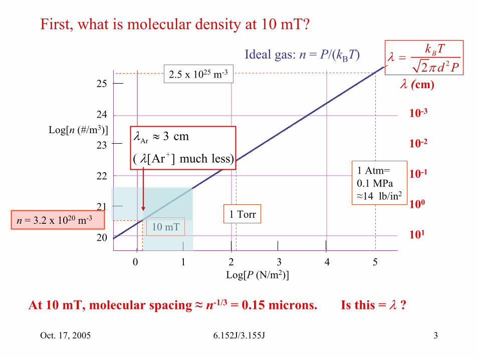
First, what is molecular density at 10 mT?
0 1 2 3 4 5Log[P (N/m2)]
25
24Log[n (#/m3)]
23
22
21
20
1 Atm=0.1 MPa≈14 lb/in2
2.5 x 1025 m-3
1 Torr10 mTn = 3.2 x 10²⁰ m-3
Ideal gas: n = P/(kBT)
λ (cm)
10-3
10-2
10-1
100
101
λ =kBT
2π d 2 P
λAr ≈ 3 cm
( λ[Ar+] much less)
At 10 mT, molecular spacing ≈ n-1/3 = 0.15 microns. Is this = λ ?

Oct. 17, 2005 6.152J/3.155J 4
Spacing between molecules ≈ n-1/3 = 0.15 microns.
λAr ≈ 3 cm
( λ[Ar+] much less)λ =
kB T2πd 2P
Thermal velocity of Ar, ≈ 103 m/sv ≈3kB Tm Ar
What’s final velocity of ions at x = λ? E field accelerates Ar+, e- between collisions.
v f2 = v0
2 + 2ax ≈ 2Eqm
λ ve− ≈ 2 ×10⁷ m/s,vAr ≈ 4 ×10⁵ m/s
(only 0.1% to 1% of nAr are ions):

Oct. 17, 2005 6.152J/3.155J 5
v ≈3kB Tm Ar
vkT ≈ 103 m/svAr+ ≈ 4 × 10⁵ m/sve- ≈ 2 × 10⁷ m/s
Be clear about different velocities:
cathode anode
⊕V ≈ 1 kV
-Ex ve−vAr+
Ionization event
So we have: low-vel. Ar+ high vel. e-
J = nqv x Thus Je- >> JAr+
The plasma is highly conducting due to electrons:
Je− = σE = nqv x ≈ nq at2
≈ nq Eq2m
λv
σ e− ≈nq2
2mλv
=ne2τ2m

Oct. 17, 2005 6.152J/3.155J 6
Plasma is self-sustaining only for 1 or 10 mT < P < 100 mT.
“Why this pressure range?”
Necessary conditions:
12
mv f2 = 2ax ≈ Eqλ
If pressure is too high, λ is small, very little acceleration between collisions
λ =kBT
2π d 2 P
If pressure is too low, λ is large, too few collisions in plasma to sustain energy
2) EK > ionization potential of Ar+
1) λ < L so collisions exchange energy
within plasma

100 V 1000 V
-1 0 1 2 3 4 5Log[P (N/m2)]
Log[λ (m)]0
-1
-2
-3
-4
-5
10 mT: λ ≈ 3 cm
λ =kBT
2π d 2 P12
mv f2 ≈ Eqλ ≈
VL
λ(eV)
EK (eV)2
1
0
-1
-2
-3
Ne+ 22Ar+ 16Kr+ 13
Self-sustained plasma
Plasma is self-sustaining only for 1 or 10 mT < P < 100 mT.
2) EK > Ar+
λ ≈ 3 cm: EK ≈ 0.3 x V
1) λ < L ≈ 10 cm
Oct. 17, 2005 6.152J/3.155J 7
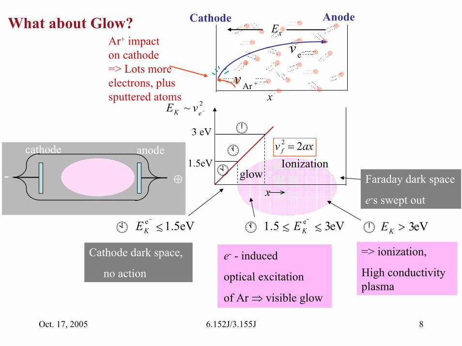
v e−
v Ar +
Ex
Cathode Anode
x
Ar+ impact on cathode=> Lots more electrons, plus sputtered atoms
x
1.5eV
EK ~ ve −2
3 eV
Ionizationglow
v f2 = 2ax
EKe −
<1.5eV~
Cathode dark space,
no action
1.5 < EKe−
< 3eV~ ~
e- - induced
optical excitation
of Ar ⇒ visible glow
cathode anode
⊕-
What about Glow?
EK > 3eV
=> ionization,
High conductivity plasma
Faraday dark space
e-s swept out
Oct. 17, 2005 6.152J/3.155J 8

Oct. 17, 2005 6.152J/3.155J 9
x
1.5eV
EK ~ ve −2
3 eV
Ionizationglow
Inside a plasma
(D.C. or “cathode sputtering”)
cathode anode
⊕-J e− , v e− >> J Ar + ,v Ar + ⇒
Surfaces in plasma charge negative, attract Ar+ repel e-
∴ plasma ≈ 10 V positive
relative to anode
Cathode sheath: low ion density
PlasmaHigh conductivity
Cathode Anode
e-
Ar++ VD.C.
Target species
Target
Substrate

Oct. 17, 2005 6.152J/3.155J 10
Which species, e- or Ar+ , is more likely to dislodge an atom at electrode ?
P ≈ 10-100 m Torrcathode anode
⊕V ≈ 1 kV
-Ex ve−vAr+
At 1 keV, vAr+ = ve/43
P ≈ 10-100 m Torrcathode anode
⊕V ≈ 1 kV
-Ex ve−vAr+
Cathode is “target”,source material
Sputter removal (etching) occurs here
pe = mvMomentum transfer: PAr = MV = 1832mv/43 ≈ 43pe-
No surprise. from ion implantation,
most energy transfer when:i.e. incoming particle has mass
close to that of target.
∆E = E14M1M2
M1 + M2( )2

Oct. 17, 2005 6.152J/3.155J 11
Sputtering processAr+ impact, momentum transfer at cathode ⇒ 1) e- avalanche and
2) released target atoms, ions.
Elastic energy transfer
E2
E1
∝4M1M2
M1 + M2( )2 cos2 θ E2 greatest for M1 ≅ M2θ
E1
E2
Atomic billiards
For e- hitting anode, substrate, M1 < < M2E2
E1
≈4M1
M2
(small)
But e- can give up its EK in inelastic collision: 12
meve2 ⇒ ∆U Excitation of atom or ion

Oct. 17, 2005 6.152J/3.155J 12
Sputtering process: ablation of target
P ≈ 10-100 m Torrcathode anode
⊕V ≈ 1 kV
-Ex ve−vAr+
Cathode is “target”,source material
cathode anode
⊕V ≈ 1 kV
-
Mostly-neutral source atoms(lots of e’s around)
Target material (cathode) must be conductive…or must use RF sputtering
(later)
Momentum transfer of Ar+
on cathode erodes cathode atoms
⇒ flux to anode, substrate.
Ar+
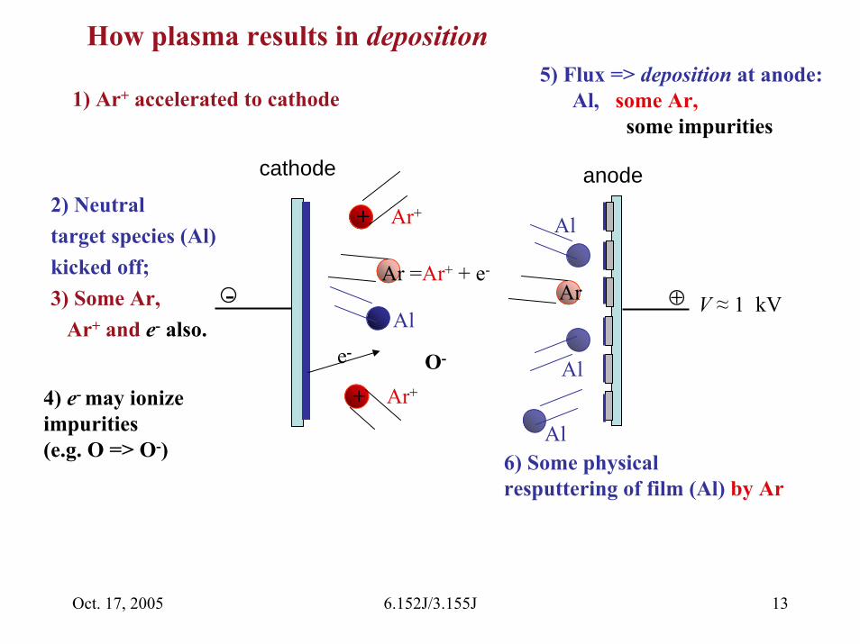
Oct. 17, 2005 6.152J/3.155J 13
cathode
⊕ V ≈ 1 kV
anode
-
Al
Ar
Al
+ Ar+
+ Ar+
1) Ar+ accelerated to cathode
Al
Ar =Ar+ + e-
e-
2) Neutral target species (Al) kicked off;3) Some Ar,
Ar+ and e- also.
4) e- may ionize impurities (e.g. O => O-)
O-
5) Flux => deposition at anode:Al, some Ar,
some impurities
6) Some physicalresputtering of film (Al) by Ar
Al
How plasma results in deposition

Oct. 17, 2005 6.152J/3.155J 14
Sputtering rate of source material in target is key parameter. Typically 0.1 - 3 target atoms released/Ar incident
Sputtering rates vary little from material to material.
Vapor pressure of source NOT important (this differs greatly for different materials).
cathode anode
⊕ V ≈ 1 kV-
Al
Ar
Al
+ Ar+
+ Ar+
Al
Ar =Ar+ + e-
6) Some physicalresputtering of Al by Ar
2) Neutral target species (Al) kicked off.
Alcos θ
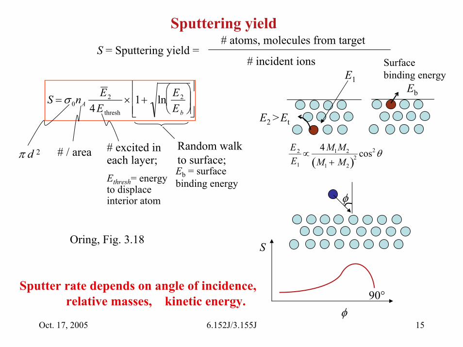
Oct. 17, 2005 6.152J/3.155J 15
S = Sputtering yield =# atoms, molecules from target
# incident ions
S = σ 0nAE 2
4E thresh
× 1+ ln E2
Eb
⎛
⎝ ⎜
⎞
⎠ ⎟
⎡
⎣ ⎢ ⎢
⎤
⎦ ⎥ ⎥
# excited in each layer;Ethresh= energy to displace interior atom
# / areaπ d 2Random walk to surface;Eb = surface binding energy
Sputtering yield
φ
S
90°
Oring, Fig. 3.18
φ
Sputter rate depends on angle of incidence,relative masses, kinetic energy.
Surface binding energy
Eb
E1
E2 >Et
E2
E1
∝4M1M2
M1 + M2( )2 cos2 θ

Oct. 17, 2005 6.152J/3.155J 16
Table 3-4 in Ohring, M. The Materials Science of Thin Films. 2nd ed. Burlington, MA: Academic Press, 2001. ISBN: 0125249756.
Figure removed for copyright reasons.

Oct. 17, 2005 6.152J/3.155J 17
Figure 12.13 in Campbell, S. The Science and Engineering of Microelectronic Fabrication. 2nd ed. New York, NY: Oxford University Press, 2001. ISBN: 0195136055.
Sputter yield vs. ion energy, normal incidence
Figure removed for copyright reasons.

Sputtering miscellany
Isotropic flux:cos θ = normal component
of flux
Higher P
Anisotropic flux:cosn θ: more-narrowly
directed at surface(surface roughness)Poor step coverage. Lower P
Large target, small substrate => Good step coverage,
more uniform thicknessMoving substrates
Higher pressure => shorter λ, better step coverage
…but more trapped gas
λ =kB T
2πd 2Pp λ (cm)
10 mT 2 1 mT 20
Oct. 17, 2005 6.152J/3.155J 18

Oct. 17, 2005 6.152J/3.155J 19
Target composition vs. film compositionSputtering removes outer layer of target;
can lead to problem with multi-component system, but only initially
A3BA2.5B A2B
If sputter yield A > B
time
Surface compositionof target
A
B
Initial target composition A3B
Another approach:Co-sputtering => composition control;
multiple targets & multiple guns. Also can make sample “library”.
A2B AB AB2
A B
Deposited film initially richer in A than target; film composition eventually correct.

Oct. 17, 2005 6.152J/3.155J 20
Varieties of sputtering experienceD.C. sputter deposition: Only for conducting materials.
if DC sputtering were used for insulator. e.g. carbon, charge would accumulate at each electrode and quench plasma within 1 - 10 mico-sec.
+ Ar+
cathode anode
⊕ V ≈ 1 kV-
C
Ar
Ct < 1 micro sec
C
Ar =Ar+ + e-
e- O-
What does 1 microsectell you about ion speed? (>106 cm /sec)
Therefore, use RF plasma…RF -sputter system is basically a capacitor with gas dielectric. Energy density ↑ as f ↑

Oct. 17, 2005 6.152J/3.155J 21
RF plasma sputteringTarget
Substrate
Vplasma
Plasma potential still V > 0 due to high e- velocity, (-) charging of surfaces. Potential now symmetric.
ω p ~ 10 7s−1Plasma conducts at low f
Thus, V = 0 in plasma
Mobility of target species (concentration gradient )still => sputtering in 1/2 cycle:
v ≤2eVM
≈ 7 ×10⁴ m /s
Target
Substrate
Vplasma
Smaller target => higher field
+ Ar+ Ar+ +
Some re-sputteringof wafer
V1
V2
=A2
A1
⎛
⎝ ⎜
⎞
⎠ ⎟
m
m ≈ 1,2
F.C.C. reserves: 13.56 MHz for sputtering

RF Bias sputtering
Negative wafer bias enhances re-sputtering of film
Varieties of sputtering experience
Target
Substrate
Vplasma
+ Ar+
Vbias ≈-100 V
Ar+ +
Some re-sputteringof wafer
V ≈-1 kV
Bias is one more handle for process control. Used in SiO2: denser,
fewer asperities.Bias affects stress, resistivity,
density, dielectric constant…
Figure 3-24 in Ohring, 2001.
Oct. 17, 2005 6.152J/3.155J 22
Figure removed for copyright reasons.

Oct. 17, 2005 6.152J/3.155J 23
Cathode
-Vbias
Film stress in RF sputter deposition
Film Species
Better step coverage
Ar+

Oct. 17, 2005 6.152J/3.155J 24
Varieties of sputtering experience
B
F
Magnetron sputtering use magnets
S
N S
N
N
S
Cathode target
ur= q v
v× B
ur( )+ Exq F =mv2
r, r =
mvqB
vz Bx ⇒ Fy ⇒ vy
v ≈ 6 × 10⁶ m/s for electron, r < 1 mm for 0.1 T
Ions spiral around B field linesvy Bx ⇒ Fz ⇒ vz
B field enhances time of e- in plasma
⇒ more ionization, greater Ar+ density.
V+
Ex
v0

Reactive sputter deposition: Mix reactive gas with noble gas (Ar or Ne).
analogous to PECVD
TiN
Ti or TiN target
Ar +N2
Also useful for oxides: SiOx, TiO, CrO…other nitrides: SiN, FeN,…
Oct. 17, 2005 6.152J/3.155J 25
Oct. 17, 2005 6.152J/3.155J 26
Figure 12.27 in Campbell, 2001.
Resistivity and composition of reactivity sputtered TiN vs. N2 flow.
Figure removed for copyright reasons.

Oct. 17, 2005 6.152J/3.155J 27
Thin film growth details (R < 1)
1) Arrival rate,physical
adsorption
2) Surfacediffusion
3) Chemicalreaction
4) Nucleation
5) Growth
6) Bulk diffusion
R≡
Rate of arrivalDiffusion rate
If R > 1, these processes have reduced probability
Anode

Oct. 17, 2005 6.152J/3.155J 28
Sputtering metals Can use DC or RF
Sputter alloys, compounds Concern about different sputter yield S
But S does not vary as much as Peq.vapwhich controls evaporation
e.g. Al Si
S = 1.05 0.5
Sputter target T < < Tevap
No diffusion, surface enriched in low S components
High diffusion,
composition change, species
distributed over entire source

Oct. 17, 2005 6.152J/3.155J 29
Table 3-7 in Ohring, 2001.Figure removed for copyright reasons.