JoNSNEA Paper Copper Nanowires (2011) (1)
16
Journal of NanoScience, Nanoengineering & Applications Volume 1, Issue 1, February, 2011, Pages 1-16. _____________________________________________________________________________________________ © STM Journals 2011. All Rights Reserved. 1 Fabrication and Characterization of Copper Nanowires: An Overview Hardev Singh Virk Nanotechnology Laboratory, DAV Institute of Engineering & Technology, Kabir Nagar, Jalandhar, India Author for Correspondence Email: [email protected] ; Cell Phone: 91-9417553347; Fax: 91-181-2205852 ABSTRACT Copper (Cu) is one of the most important metals in modern electronic technology. Keeping in view its role in nanoelectronics, we have fabricated copper nanowires of diameters 100 and 200 nm using Anodic Alumina and polymer membranes as templates. Template-based growth of copper nanowires has been realized using conventional electro deposition technique in an electrochemical cell designed in our laboratory. Fabrication of copper nanowires is one of the most important thrust areas of nanotechnology because of their potential use in the micro/nanoelectronics industry and, in particular, for interconnection in electronic circuits. Many methods have been developed for the fabrication of copper nanowires but template synthesis is considered to be the most suitable and useful for growth of nanowires. Electrochemical deposition route is easy, low-cost as well as less cumbersome compared to other fabrication techniques, namely, pulsed laser deposition (PLD), vapour-liquid-solid (VLS) method and chemical vapour deposition (CVD). Scanning Electron Microscope (SEM) is used to calculate the aspect ratio of nanowires. Field Emission Scanning Electron Microscope (FESEM) images and Energy Dispersive X-ray Analysis (EDX) reveal morphology and chemical composition of fabricated nanowires. The morphology of nanowires shows some interesting features. X-ray diffraction (XRD) spectrum reveals crystalline nature of Cu nanowires with crystallite size of 1.12 nm. During our experiments, we observed that when we failed to fabricate nanowires in polymer templates, what we got was some exotic patterns of metallic copper in the shape of copper buds and flowers on the cathode surface. There is as yet no specific theory to explain exotic patterns developed during electrodeposition of copper in anodic alumina or polymer templates. It is speculated that overdeposition of copper results in formation of exotic patterns. Keywords: Electrodeposition, Anodic alumina membrane, Cu nanowires, nanoflowers and nanobuds, Polycrystalline Cu crystals, XRD.
-
Upload
sehati-fisika -
Category
Documents
-
view
217 -
download
0
Transcript of JoNSNEA Paper Copper Nanowires (2011) (1)

Journal of NanoScience, Nanoengineering & Applications
Volume 1, Issue 1, February, 2011, Pages 1-16.
_____________________________________________________________________________________________
© STM Journals 2011. All Rights Reserved. 1
Fabrication and Characterization of Copper Nanowires: An Overview Hardev Singh Virk
Nanotechnology Laboratory, DAV Institute of Engineering & Technology,
Kabir Nagar, Jalandhar, India
Author for Correspondence Email: [email protected]; Cell Phone: 91-9417553347;
Fax: 91-181-2205852
ABSTRACT
Copper (Cu) is one of the most important metals in modern electronic technology. Keeping
in view its role in nanoelectronics, we have fabricated copper nanowires of diameters 100
and 200 nm using Anodic Alumina and polymer membranes as templates. Template-based
growth of copper nanowires has been realized using conventional electro deposition
technique in an electrochemical cell designed in our laboratory. Fabrication of copper
nanowires is one of the most important thrust areas of nanotechnology because of their
potential use in the micro/nanoelectronics industry and, in particular, for interconnection in
electronic circuits. Many methods have been developed for the fabrication of copper
nanowires but template synthesis is considered to be the most suitable and useful for
growth of nanowires. Electrochemical deposition route is easy, low-cost as well as less
cumbersome compared to other fabrication techniques, namely, pulsed laser deposition
(PLD), vapour-liquid-solid (VLS) method and chemical vapour deposition (CVD).
Scanning Electron Microscope (SEM) is used to calculate the aspect ratio of nanowires.
Field Emission Scanning Electron Microscope (FESEM) images and Energy Dispersive
X-ray Analysis (EDX) reveal morphology and chemical composition of fabricated
nanowires. The morphology of nanowires shows some interesting features. X-ray
diffraction (XRD) spectrum reveals crystalline nature of Cu nanowires with crystallite size
of 1.12 nm. During our experiments, we observed that when we failed to fabricate
nanowires in polymer templates, what we got was some exotic patterns of metallic copper
in the shape of copper buds and flowers on the cathode surface. There is as yet no specific
theory to explain exotic patterns developed during electrodeposition of copper in anodic
alumina or polymer templates. It is speculated that overdeposition of copper results in
formation of exotic patterns.
Keywords: Electrodeposition, Anodic alumina membrane, Cu nanowires, nanoflowers
and nanobuds, Polycrystalline Cu crystals, XRD.

Journal of NanoScience, Nanoengineering & Applications
Volume 1, Issue 1, February, 2011, Pages 1-16.
_____________________________________________________________________________________________
© STM Journals 2011. All Rights Reserved. 2
1. Introduction
Synthesis, characterization and application
of nanowires and nanotubes comprise a
significant aspect of today’s endeavor in
nanotechnology. During recent years,
nanowires and nanorods of metallic and
semi-conducting materials have drawn a lot
of research interest because of their potential
applications in diverse fields, for example,
nanoelectronics, opto-electronics and
sensors [1-3]. The special features of
nanowires are defined by two quantum-
confined dimensions allowing free flow of
current in one dimension only. In nanowires,
electronic conduction takes place both by
bulk conduction and through tunneling
mechanism. However, due to their high
density of electronic state, diameter-
dependant band gap, enhanced surface
scattering of electrons and phonons,
increased excitation energy, high surface to
volume ratio and large aspect ratio,
nanowires of metals and semiconductors
exhibit unique electrical, magnetic, optical,
thermoelectric and chemical properties
compared to their bulk counterpart [1].
Template-based growth is a versatile method
of synthesis of metallic and semiconductor
nanowires. Many studies have focused on
the fabrication of copper nanowires [4-8],
because of their potential applications in the
micro/nanoelectronics industry and, in
particular, for interconnection in electronic
circuits. A recent study [9] has established
that copper nanowires could revolutionize
the development and production of low-cost
flexible displays, light emitting diodes and
thin film solar cells. Copper is one of the
most important metals in modern electronic
technology. Copper is 1000 times more
abundant than indium or silver, and is 100
times less expensive. As a consequence,
films of copper nanowires represent a low-
cost alternative to silver nanowires or
indium tin oxide (ITO) for use as a
transparent electrode.
Many methods have been developed for the
fabrication of copper nanowires but template
synthesis is considered to be most suitable
and useful for growth of nanowires.
Electrochemical deposition route is easy,
low-cost as well as less cumbersome
compared to other fabrication techniques
[1], namely, pulsed laser deposition (PLD),
vapour-liquid-solid (VLS) method and
chemical vapour deposition (CVD).
Electrochemical cell used in
electrodeposition of copper into pores of
anodic alumina template was fabricated in
our laboratory. Morphology of
electrodeposited copper nanowires has been
studied using Field Emission Scanning
Electron Microscopy (FESEM). The
diameter of nanowires generally depends
upon the pore size of template. Anodic
alumina discs of 200 nm and polymer
membranes of 100 nm pore diameter were
selected for this purpose.
Template materials must meet certain
requirements [4]. First, the template
materials must be compatible with the
processing conditions. For example, an
electrical insulator is required for a template
to be used in electrochemical deposition.
Template materials should be chemically
and thermally inert during the synthesis.
Secondly, depositing materials or solution
must wet the internal pore walls. Thirdly, for
synthesis of nanowires, the deposition
should start from the bottom of the template
and proceed upwards to the other side. This
is known as bottom up technique in
nanotechnology.

Journal of NanoScience, Nanoengineering & Applications
Volume 1, Issue 1, February, 2011, Pages 1-16.
_____________________________________________________________________________________________
© STM Journals 2011. All Rights Reserved. 3
Template-based synthesis offers many
advantages over other methods of synthesis
[10]: (1) It is performed under mild
conditions rather than requiring high
temperatures, high vacuum or expensive
instrumentation; (2) templated electro-
deposition has a relatively high growth rate;
(3) the morphology of deposited materials
depends on the shape of template pores; (4)
the dimensions of the materials obtained can
be tuned by tuning of the template pore size;
(5) two or more components can be easily
deposited into the membrane sequentially to
form multi-segmented materials or hetero-
junctions.
2. Materials and Methods
The electro-deposition technique used in our
experiment [11] is similar in principle to that
used for the electroplating process.
Commercial anodic alumina membranes
(AAM) (anodisc 25 made by Whatman)
having an average pore diameter of 200 nm,
a nominal thickness of 60 µm and a pore
density of 109 pores/ cm
2, were used as
templates. A second set of experiments was
performed using polymer membranes
(Sterlitech USA) of 100 nm and 20 nm pore
diameters. To achieve uniform deposition
of nanowires, templates were cleaned in the
ultrasonic bath for 10 minutes. The
electrochemical cell, fabricated in our
laboratory using Perspex sheets, was washed
in double distilled water. A copper rod of
0.8 cm diameter was used as a sacrificial
electrode (anode). The cathode consists of
copper foil attached to alumina disc by an
adhesive tape of good conductivity. Prior to
the electro-deposition process, a thin film of
copper (0.5 µm) was coated onto one side of
alumina disc by thermal evaporation
technique using Thin Film Coating Unit.
This metal layer along with adhesive copper
tape provides a stable substrate (cathode) for
the growth of nanowires. Polymer
membranes were damaged during thermal
evaporation of copper and used as received,
or after coating with silver paste manually,
for electro-deposition.
The electrolyte used had a composition of
20 gm/100ml CuSO4.5H2O + 25% of dilute
H2SO4 at room temperature. The inter-
electrode distance was kept 0.5 cm and a
current of 2 mA was applied for 10 minutes
using APLAB power supply. Electro-
deposition of copper nanowires depends on
many factors, namely, inter-electrode
spacing, electrolyte composition,
temperature and pH value, current density
and time of deposition. The influence of
current density, temperature and type of
electrolyte on the crystallinity of copper
nanowires has been reported elsewhere [12].
During our experiments, pH value was
adjusted between 4-5, deposition
temperature between 30-500C and we
studied the effect of current density on
electro-deposition of copper nanowires by
varying the current between 2-3 mA.
After the electro-deposition was over,
copper foil with template-grown nanowires
was kept immersed in 1 M NaOH for 1 hour
in a beaker to dissolve alumina template.
The copper nanowires were liberated from
the host matrix, washed in distilled water
and dried in an oven at 500C for 30 minutes.
The cleaned and dried nanowires were
mounted on aluminium stubs with the help
of double adhesive tape. FESEM (Hitachi S-
4300) was used to record cross-sectional and
lateral views of grown nanowires at an
accelerating voltage of 15 kV using different
magnifications. X-ray Diffraction studies
were carried out at Sophisticated Analytical

Journal of NanoScience, Nanoengineering & Applications
Volume 1, Issue 1, February, 2011, Pages 1-16.
_____________________________________________________________________________________________
© STM Journals 2011. All Rights Reserved. 4
Instruments Facility (SAIF) set up by Punjab
University, Chandigarh using X' Pert PRO
(PANanalytical, Netherlands) employing Cu
Kradiation source of λ = 1.5406 Å.
3. Results and Discussion
3.1 AFM, SEM and FESEM Analysis
Commercial available templates were
examined before their use using Atomic
Force Microscope (NT-MDT PR 400
Model) installed in our laboratory and
Scanning Electron Microscope (Jeol, JSM
6100) facility of Punjab University,
Chandigarh. Atomic force microscopic
technique [13] shows the two dimensional
surface topology of the anodic alumina
template with hexagonal pores regularly
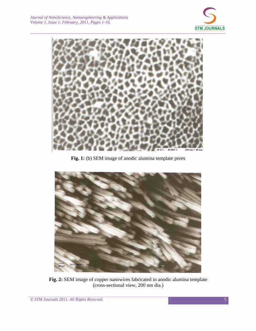
arranged on the surface (Fig. 1a). The pores
appear nearly at the centre of each
hexagonal cell. After gold sputtering, using
Jeol sputter JFC 1100, SEM micrograph
(Fig. 1b) shows the geometrical pattern of
pores on the alumina surface of anodisc.
Fig. 1: (a) AFM image of hexagonal pores of anodic alumina template
Journal of NanoScience, Nanoengineering & Applications
Volume 1, Issue 1, February, 2011, Pages 1-16.
_____________________________________________________________________________________________
© STM Journals 2011. All Rights Reserved. 5
Fig. 1: (b) SEM image of anodic alumina template pores
Fig. 2: SEM image of copper nanowires fabricated in anodic alumina template
(cross-sectional view, 200 nm dia.)

Journal of NanoScience, Nanoengineering & Applications
Volume 1, Issue 1, February, 2011, Pages 1-16.
_____________________________________________________________________________________________
© STM Journals 2011. All Rights Reserved. 6
Fig. 3: (a) SEM image of copper nanowires Fig. 3: (b) SEM image of copper nanowires
fabricated in AAM under constant current under transient current with capping effect
Copper nanowires liberated from AAM
were examined under SEM and FESEM
under different magnifications. Two sets of
templates were used for growth of copper
nanowires. In one set, current density was
changed intermittently which resulted in
non-uniform growth of nanowires. Figure 2
represents the cross-sectional view of copper
nanowires of 200nm diameter grown in
alumina template. Figure 3(a) shows the
SEM image of copper nanowires array in
lateral view, grown under constant current
conditions. Figure 3(b) represents the
FESEM image of copper nanowires
fabricated under transient current conditions,
current constantly varied between 2-3 mA.
Over-deposition of copper is clearly visible
towards the tip of nanowires resulting in
capping effect. Nanowires are quite uniform
with diameter in the range of 200 nm but
they are not perfect cylinders. It has been
reported [14] that pore diameters of
commercially available templates vary over
a large range. The aspect ratio, that is, the
ratio of length to diameter, is on the order of
300.
Electro-deposition of copper nanowires was
achieved using polycarbonate membrane
with pore diameter of 100 nm as a template
and keeping the other conditions identical
[11]. Silver paste was coated on the back of
polymer template to make it conducting.
The polymer template was dissolved in
dichloromethane at room temperature. SEM
micrograph of grown copper nanowires is
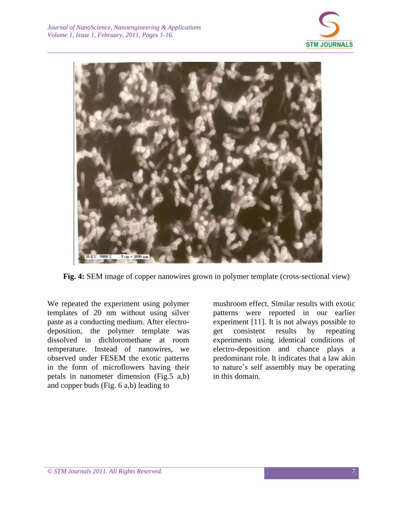
shown in Fig. 4. The cross-sectional view of
nanowires is somewhat of poor quality and
not as smooth as in case of alumina
templates.
Journal of NanoScience, Nanoengineering & Applications
Volume 1, Issue 1, February, 2011, Pages 1-16.
_____________________________________________________________________________________________
© STM Journals 2011. All Rights Reserved. 7
Fig. 4: SEM image of copper nanowires grown in polymer template (cross-sectional view)
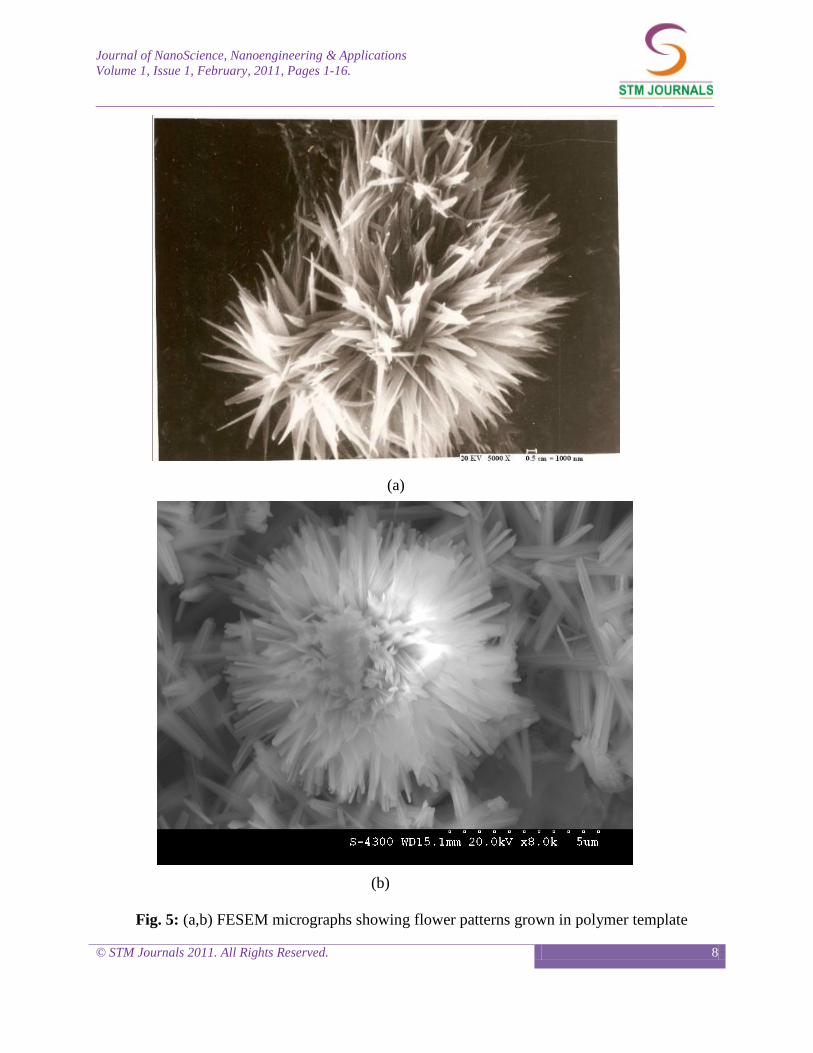
We repeated the experiment using polymer
templates of 20 nm without using silver
paste as a conducting medium. After electro-
deposition, the polymer template was
dissolved in dichloromethane at room
temperature. Instead of nanowires, we
observed under FESEM the exotic patterns
in the form of microflowers having their
petals in nanometer dimension (Fig.5 a,b)
and copper buds (Fig. 6 a,b) leading to
mushroom effect. Similar results with exotic
patterns were reported in our earlier
experiment [11]. It is not always possible to
get consistent results by repeating
experiments using identical conditions of
electro-deposition and chance plays a
predominant role. It indicates that a law akin
to nature’s self assembly may be operating
in this domain.
Journal of NanoScience, Nanoengineering & Applications
Volume 1, Issue 1, February, 2011, Pages 1-16.
_____________________________________________________________________________________________
© STM Journals 2011. All Rights Reserved. 8
(a)
(b)
Fig. 5: (a,b) FESEM micrographs showing flower patterns grown in polymer template

Journal of NanoScience, Nanoengineering & Applications
Volume 1, Issue 1, February, 2011, Pages 1-16.
_____________________________________________________________________________________________
© STM Journals 2011. All Rights Reserved. 9
(a)
(b)
Fig. 6: (a,b) FESEM micrographs showing copper buds grown in polymer template

Journal of NanoScience, Nanoengineering & Applications
Volume 1, Issue 1, February, 2011, Pages 1-16.
_____________________________________________________________________________________________
© STM Journals 2011. All Rights Reserved. 10
There is as yet no specific theory to explain
exotic patterns developed during electro-
deposition of copper in anodic alumina or
polymer templates. A speculative
explanation [15] is provided on the basis of
over-deposition. During the growth of
copper nanowires in the template pores, the
current remains nearly stable until the wires
arrive at the template surface. If the electro-
deposition process is not stopped at this
stage, the current keeps on rising very
gradually leading to over-deposition of
copper. Flower like morphologies of metal
overdeposits have been attributed to the
changes in hydrodynamic conditions due to
excessive hydrogen evolution during
electro-deposition process [16].
Fig. 7: SEM micrograph of pyramid shaped polycrystalline copper crystals
During our experiments using 20 nm pore
diameter polycarbonate template, we had a
big surprise in store beyond our
imagination! The template was not coated
with a conducting layer during electro-
deposition. It resulted in failure to grow
nanowires but the failure of experiment
proved to be a blessing in disguise. Instead
of copper nanowires, we observed growth of
double pyramid shaped copper crystals (Fig.
7). We could not find any evidence for this
phenomenon in published literature on
electro-deposition of nanowires.

Journal of NanoScience, Nanoengineering & Applications
Volume 1, Issue 1, February, 2011, Pages 1-16.
_____________________________________________________________________________________________
© STM Journals 2011. All Rights Reserved. 11
3.2 X-ray and EDX Analysis
The crystal structure of these pyramid
shaped copper crystals has been determined
using X-ray diffraction analysis. XRD
spectrum (Fig. 8) shows two prominent
peaks corresponding to 2θ = 43.4610 and
50.5803, with d spacing = 2.082 and 1.804,
respectively. These peaks reveal the
polycrystalline nature of copper crystals,
indicating that preferred growth direction of
crystals is the (200) plane. Template based
synthesis of single crystal copper nanowires
has been reported in literature [12,15,17]
with preferred growth direction along (111)
plane, but to the best of our knowledge,
there is hardly any report for pyramid-
shaped polycrystalline copper crystals with a
(200) preferred orientation.
Position [°2Theta] (Copper (Cu))
10 20 30 40 50 60 70
Counts
0
20000
40000
60000
36.6
37 [
°]
38.2
83 [
°]
43.4
61 [
°]
45.4
48 [
°]
48.9
20 [
°]
50.5
80 [
°]
54.3
04 [
°]54.9
56 [
°]
64.8
09 [
°]
74.2
99 [
°]
KK1
Fig. 8: XRD spectrum of pyramid-shaped polycrystalline copper crystals

Journal of NanoScience, Nanoengineering & Applications
Volume 1, Issue 1, February, 2011, Pages 1-16.
_____________________________________________________________________________________________
© STM Journals 2011. All Rights Reserved. 12
The crystallographic structure of copper
nanowire arrays was investigated by X-ray
diffraction analysis (XRD). For sake of
comparison, XRD spectrum of Cu foil used
as a substrate was also recorded (Fig. 9).
XRD diffractograms were obtained in the 2θ
range from 100 to 80
0 with a step of 0.02
0,
using the Cu Kradiation source of λ =
1.5406 Å. XRD spectrum (Table 1) shows
three prominent peaks corresponding to 2θ =
43.5966, 50.8127 and 74.4331, with d
spacing = 2.074, 1.80 and 1.27, and
corresponding Miller indices, (111), (200)
and (220), respectively. All the peaks can be
attributed to the crystalline cubic form of
metallic copper [6] and can be indexed to
Card ICSD # 064699.
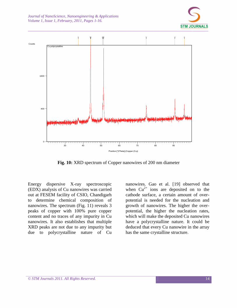
XRD diffractogram (Fig. 10) for copper
nanowires was obtained in the 2θ range from
100 to 100
0 with a step of 0.02
0, keeping
other parameters same as above. There are in
all 9 peaks in the spectrum (Table 2), with
one insignificant peak at 2θ= 37.3222, which
may be due to Cu2O impurity. Three main
peaks are also there as in Fig. 9 but two of
them split into double and triple peaks,
which may be attributed to X-ray scattering
at the substrate. The presence of five
prominent diffraction peaks at 2θ angles of
44.1976, 51.3448, 74.8869, 90.6580 and
95.9099 with the most prominent peak at
These peaks correspond to Cu (111), Cu
(200), Cu (220), Cu (311) and Cu (222),
respectively, indicating that the preferred
growth direction of nanowires is the (111)
plane. The strong and sharp peaks indicate
that copper nanowires have high degree of
crystalline order. All the intense XRD peaks
in spectrum (Fig. 10) correspond to and
match perfectly with those of polycrystalline
Cu standard (Card # ICDD 001-1242).
Template based synthesis of single crystal
copper nanowires have also been reported in
literature [15, 17] with preferred growth
direction along (111) plane.
The average size D of the crystalline grains
in the Cu nanowires is calculated using the
Debye Scherrer’s formula [18]: D = 0.9 λ /
β cos θ, where λ=1.5406 Å is the wavelength
of the X-ray radiation used, β is the full
width at half maximum (FWHM) of the
diffraction peak (0.1338), K, shape factor is
assumed to be 0.9 and θ is the Bragg
diffraction angle of the most prominent XRD
peak. Substituting appropriate values in the
formula, the crystallite size value of Cu
nanowires comes out to be 1.12 nm.
However, the value of crystallite size
calculated for Cu foil is of the order of 2.44
nm.
2θ=44.1976, reveals that the Cu nanowires
with face-centered cubic (fcc) crystal
structure had been fabricated.

Journal of NanoScience, Nanoengineering & Applications
Volume 1, Issue 1, February, 2011, Pages 1-16.
_____________________________________________________________________________________________
© STM Journals 2011. All Rights Reserved. 13
Position [°2Theta] (Copper (Cu))
10 20 30 40 50 60 70
Counts
0
5000
10000 Cu
Table 1. XRD spectrum peaks data of copper film
Table 2. XRD spectrum peaks data of copper nanowires
Pos. [°2Th.] FWHM [°2Th.] d-spacing [Å] Rel. Int. [%] Area [cts*°2Th.]
37.3222 0.4015 2.40741 1.81 32.89
44.0674 0.1224 2.05330 73.55 550.50
44.1976 0.1338 2.04755 100.00 605.43
50.7219 0.1338 1.79842 9.18 55.58
51.0435 0.0612 1.78784 16.51 61.77
51.3448 0.0816 1.77806 75.85 378.50
74.8869 0.2448 1.26698 7.01 104.91
90.6580 0.2040 1.08317 10.76 134.23
95.9099 0.1428 1.03727 6.50 56.79
Fig. 9: XRD spectrum of Copper film serving as a substrate
Pos. [°2Th.] FWHM [°2Th.] d-spacing [Å] Rel. Int. [%] Area [cts*°2Th.]
43.5966 0.0612 2.07438 100.00 847.65
50.8127 0.0816 1.79542 48.53 548.43
74.4331 0.1428 1.27358 11.94 236.07
Journal of NanoScience, Nanoengineering & Applications
Volume 1, Issue 1, February, 2011, Pages 1-16.
_____________________________________________________________________________________________
© STM Journals 2011. All Rights Reserved. 14
Position [°2Theta] (Copper (Cu))
30 40 50 60 70 80 90
Counts
0
400
1600
Cu polycrystalline
Fig. 10: XRD spectrum of Copper nanowires of 200 nm diameter
Energy dispersive X-ray spectroscopic
(EDX) analysis of Cu nanowires was carried
out at FESEM facility of CSIO, Chandigarh
to determine chemical composition of
nanowires. The spectrum (Fig. 11) reveals 3
peaks of copper with 100% pure copper
content and no traces of any impurity in Cu
nanowires. It also establishes that multiple
XRD peaks are not due to any impurity but
due to polycrystalline nature of Cu
nanowires. Gao et al. [19] observed that
when Cu2+
ions are deposited on to the
cathode surface, a certain amount of over-
potential is needed for the nucleation and
growth of nanowires. The higher the over-
potential, the higher the nucleation rates,
which will make the deposited Cu nanowires
have a polycrystalline nature. It could be
deduced that every Cu nanowire in the array
has the same crystalline structure.

Journal of NanoScience, Nanoengineering & Applications
Volume 1, Issue 1, February, 2011, Pages 1-16.
_____________________________________________________________________________________________
© STM Journals 2011. All Rights Reserved. 15
Live Time: 100.0 sec.
Quantitative Results for: experiment 1(2)
Element Line
Weight %
Weight % Error
Atom %
Atom % Error
Cu K 100.00 +/- 7.49 100.00 +/- 7.49 Total 100.00 100.00
Fig. 11: EDX spectrum and elemental composition of Copper nanowires
4. Conclusions
Our investigations confirm that electro-
deposition of copper nanowires in anodic
alumina is the simplest route to
nanotechnology. The copper nanowires
reveal effect of high current density
resulting in over-deposition in the form of
capped growth, and not as perfect cylinders.
The aspect ratio is very high, of the order of
300. XRD analysis shows fcc crystalline
nature of nanowires with preferred growth
direction in the (111) plane. The crystallite
size of nanocrystals in copper nanowires is
determined to be 1.12 nm. Over-deposition
results in growth of copper buds and
beautiful flower patterns. Pyramid-shaped
polycrystalline copper crystals are observed
for the first time during failure to fabricate
copper nanowires using electro-deposition
technique. Due to high aspect ratio, copper
nanowires may be used as field emitters
[20]. Possible applications of nanoflowers as
optoelectronics devices or sensors, in
catalysis, and solar cells will be of definite
interest in future studies [21].

Journal of NanoScience, Nanoengineering & Applications
Volume 1, Issue 1, February, 2011, Pages 1-16.
_____________________________________________________________________________________________
© STM Journals 2011. All Rights Reserved. 16
Acknowledgements
The authors are thankful to the Principal,
DAV Institute of Engineering &
Technology, Jalandhar and DAV College
Managing Committee, New Delhi for
providing research grant to set up Research
Centre and Nanotechnology Laboratory in
Jalandhar. FESEM analysis was carried out
at CSIO, Chandigarh. Authors wish to
record their appreciation to Dr Pawan
Kapur, Director CSIO and Dr Lalit M.
Bharadwaj, Head Nanotechnology Group at
CSIO for providing research facilities. Dr
Inderpreet Kaur and her research team also
deserve my appreciation for rendering all
possible help during characterization.
Mohinder Singh and Jagtar Singh at SAIF,
PU Chandigarh provided all help in SEM
and XRD analysis of samples, respectively,
whenever I approached them.
References
1. Sarkar J. et al. Bulletin Material Science
2007. 30 (3). 271-290p.
2. Agarwal R. and Lieber C. M. Applied
Physics A 2006. 85. 209-215p.
3. Liu Chuan-Pu et al. Recent Patents on
Nanotechnology 2007. 1. 11-20p.
4. Cao D. and Liu D. Advances in Colloid
and Interface Science 2008. 136. 45-
64p.
5. Sun Shin H. et al. Materials Letters
2009. 63. 397- 399p.
6. Ingunta R. et al. Electrochemical
Commununication 2008. 10. 506-509p.
7. Fang C. et al. Journal Electrochemical
Society 2007. 154. D45- D49p.
8. Motoyama M. et al. Journal
Electroanalytical Chemistry 2005. 584.
84p.
9. Rathmell A. R. et al. Advanced Materials
2010. 22. 3558-3563p.
10. Lai M. and Riley D. J. Journal Colloid &
Interface Science 2008. 323. 203-212p.
11. Virk H. S. et al. Journal Nano Research
2010. 10. 63- 67p.
12. Toimil Molares M. E. et al. Advanced
Materials 2001. 13. 62-65p.
13. Menon L. Quantum Dots and Nanowires.
Hari Singh Nalwa and S. Bandhopadhaya
(Eds.). American Scientific Publishers.
USA. 2003. 142-187 p.
14. Schonenberger C. et al. Journal Physical
Chemistry B 1997. 101. 5497- 5505 p.
15. Gao T. et al. Journal Physics: Condensed
Matter 2002. 14. 355-363p.
16. Kumar S. et al. Superlattices and
Microstructures 2008. 43. 324-329p.
17. Mingliang. T. et al. Nano Letters. 2003.
3. 919-923p.
18. Cullity D. B. Massachusetts. USA.
Elements of X-ray Diffraction. Addison-
Wesley. 1956.
19. Gao T. et al. Applied Physics A:
Materials Science & Processing 2001.
73. 251-254p.
20. Brotz J. et al. Microstructure Analysis in
Material Science Freiberg, June 15-17.
2005.
21. Kharisov B. I. Recent Patents on
Nanotechnology 2008. 2. 190-200p.