
Copper Nanowires and Solar Cell...
15
Copper Nanowires and Solar Cell Applications Michael Brown 5/27/2010 This paper analyzes recent developments involving nanotechnology to increase the efficiency of solar cells at capturing specific wavelengths of light. Developments in this area could be the key to inexpensive and highly efficient solar cells. Quantum confinement, the key concept of this technology can be applied to current solar cells to increase efficiency, and can also allow for the design of devices from the ground up.
Transcript of Copper Nanowires and Solar Cell...

������������ ���������
Copper Nanowires and Solar Cell Applications
Michael Brown
5/27/2010
This paper analyzes recent developments involving nanotechnology to increase the efficiency of solar cells at capturing specific wavelengths of light. Developments in this area could be the key to inexpensive and highly efficient solar cells. Quantum confinement, the key concept of this technology can be applied to current solar cells to increase efficiency, and can also allow for the design of devices from the ground up.

Table of Contents Solar Cell Technology Up to Date ...............................................................................................................1
High‐efficiency cells................................................................................................................................1
Multi‐junction solar cells ....................................................................................................................1
Thin film solar cells .............................................................................................................................2
Crystalline Silicon ...............................................................................................................................2
Macro Model for Solar Cells .......................................................................................................................2
How Bandgap Energies Are Different in Nanoscale Structures...................................................................4
Classical View of Bandgap Energies ........................................................................................................4
Quantum Confinement and Discrete Energy Levels ................................. Error! Bookmark not defined.
Why Band Gap Energies are Important in Solar Cells .............................................................................6
Nanowire Effect on Band Gap and Efficiency......................................................................................7
Matching Bandgap Energy to the Sun’s Photons ................................................................................8
Nano‐Particle Effect on the Reflection Coefficient .....................................................................................8
Low Reflection Coefficient........................................................................ Error! Bookmark not defined.
Works Cited..............................................................................................................................................13
P a g e | 1
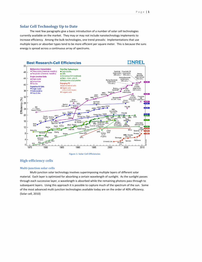
Solar Cell Technology Up to Date The next few paragraphs give a basic introduction of a number of solar cell technologies
currently available on the market. They may or may not include nanotechnology implements to
increase efficiency. Among the bulk technologies, one trend prevails: Implementations that use
multiple layers or absorber types tend to be more efficient per square meter. This is because the suns
energy is spread across a continuous array of spectrums.
Figure 1: Solar Cell Efficiencies
High‐efficiency cells
Multi‐junction solar cells
Multi‐junction solar technology involves superimposing multiple layers of different solar
material. Each layer is optimized for absorbing a certain wavelength of sunlight. As the sunlight passes
through each successive layer, a wavelength is absorbed while the remaining photons pass through to
subsequent layers. Using this approach it is possible to capture much of the spectrum of the sun. Some
of the most advanced multi‐junction technologies available today are on the order of 40% efficiency.
(Solar cell, 2010)

P a g e | 2
Thin Film solar cells
Thin Filmis a technology where instead of being laminated onto a rigid structure, photosensitive
material is manufactured onto a flexible backing. This method allows a wide variety of applications. The
current efficiency limitation for this topology is around 20%. (Solar cell, 2010)
Crystalline Silicon
Crystalline cells come in monocrystalline and polycrystalline varieties. Monocrystalline cells
have higher efficiency than polycrystalline cells but they require high quality silicon wafers, have
significant waste and cost more. (Solar cell, 2010) Solar cells using crystalline silicon structures are the
most commonly produced solar cells to date and peak out at a maximum theoretical efficiency of 29%.
Commercialized cells currently being produced by Suntech Power have been found to have an efficiency
of 22%. (Solar cell, 2010)
Macro Model for Solar Cells
Figure 2: Solar Cell Model
Current:

P a g e | 3
Equation 1: Diode Current
Equation 2: Junction Voltage
Equation 3: Shunt Current
Equation 4: Output
Current
Equation 5: Solar Cell Efficiency
Pm is the maximum power point. E is the light irradiance (W/m^2). A is the surface area of the solar cell
(m^2).

P a g e | 4
How Bandgap Energies Are Different in Nanoscale Structures The next few sections seek to explore through the electrical nature of nanostructures through
reasoning and light mathematics. At times, it may seem a more philosophical than scientific. This is
because I don’t currently possess the mathematical capability to prove these assertions explicitly. I
intend to return to this paper as my education continues to make changes and mathematical
conclusions.
Classical View of Band Gap Energies
Figure 3: Energy Levels Related to Radius
Through classical physics, we understand that the surface tension of a semiconductor is given by
the Young‐Laplace Equation. Most of the scales of typical semiconductors possess uniform density. This
uniform density provides a relatively uniform electron orbital configuration. Therefore, Bulk
semiconductors have a relatively uniform band gap density which is related to the structure of the
semiconductor lattice.
Equation 6: Young‐Laplace Equation

P a g e | 5
The Young‐Laplace equation describes the difference in pressure between a spherical structure
(assume: R1 = R2) and its surrounding environment. The main difference between bulk semiconductors
and nano‐scale semiconductors is their respective radius sizes to use with the Young‐Laplace equation.
The large surface tension in nano‐scale semiconductors changes the inter‐atomic interactions and
affects the band gap energies which increase as the structure decreases in size. (Potential well, 2010)
This Classical view assumes that the structure is still larger than the wavelength of light it is absorbing.
As the surface tension of this structure increases, it is reasonable to assume that the spacing
between atoms decreases. The decrease in space between atoms and their orbiting electrons causes
increased repulsion between electron clouds. Therefore, the energy required to reach the next
quantized energy state is increased. The Plasmon oscillation that a quantum structure sets up reflects
light of a larger wavelength, transmits light of a smaller wavelength and absorbs light of the equivalent
wavelength.
Equation 7: Free Electron Model
The free electron model can be used to estimate the Plasmon energy. (Plasmon, 2010) N is the
conduction electron density, e is the elementary charge, m is electron mass, epsilon0 is the permittivity
of space and h is the Planck constant. Wp is the frequency of the Plasmon in radians/sec.

P a g e | 6
Figure 4: Energy Levels Related to Nanoparticles
Equation 8
Equation 9: Energy Contained in Quantized Levels
Why Band Gap Energies are Important in Solar Cells Increased bandgap energies mean that a structure can contain more energy without the
possibility of that energy being converted to another type of energy (kinetic, thermal, etc.). (Potential

P a g e | 7
well, 2010) This means that while electrons are below the conduction band, entropy will be minimized,
which increases the overall efficiency of the solar cell.
Nanowire Effect on Band Gap and Efficiency
Decreasing the size of a photo collector structure increases the density of its discrete energy
states and increases the width of its bandgap. (Band gap, 2010) Where Nanowires come into play is in
creating a photo collector using a material such as Cuprous Oxide (CuO) that has attributes that the
normal bulk Cuprous Oxide doesn’t. A possible benefit of this approach is that it may be possible to
achieve the efficiencies of much more expensive solar technologies using more widely available and
inexpensive materials. Another benefit is the ability to manipulate the optical behavior of structures by
changing their size. For instance, a multijunction device similar to other solar technologies, could be
produced which has nanowires of varying dimensions. Each dimension of nanowire would have an
optimal wavelength at which it absorbed sunlight from at high efficiency.
Figure 5: Bandgap Width Relative to Density of States

P a g e | 8
Matching Band‐Gap Energy to the Sun’s Photons
We want the electrons which have been excited from the valence to the conduction band to
have uniform energies. Non uniform energies in the conduction band will cause eddy currents and
other processes that increase entropy. (Eddy Current, 2010) Any Potential difference within the
conduction band leads to small scale electromotive forces that convert electric energy into kinetic
energy and eventually create heat due to resistive loss. For this reason, we want the band gap to be
such that the incident photon has just enough energy to move the electron into the valence band. With
all potentials on the solar cell circuit uniform, a greater majority of the gathered energy will go towards
producing an overall current.
Table 1: Band‐Gap Energies of Specified Bulk Materials
Nano‐Particle Effect on the Reflection Coefficient

P a g e | 9
Figure 6: Plot of Reflectivity VS CuO Nano‐Particle Spacing
Looking at the plot shown above of the Reflectivity VS Particle Spacing, I reason that the
reflection coefficient is loosely related to the spacing between particles. Specifically, that wavelengths
that are small enough to fit in between the particles impact the silicon substrate and experience its bulk
reflectivity. Larger wavelengths don’t possess enough energy to move an electron into the conduction
band and are eventually re‐emitted as spontaneous emission.These 3 plots were borrowed from (Third
Generation Solar Cell Technologies: Localized Surface Plasmons, 2009).
Comment [AHL1]: Did the article specified that these result corresponded to uo nanoparticles?

P a g e | 10
Figure 7: Plot of Reflectivity VS CuO Nano‐Particle Sizes
From the plot of Reflectivity VS Particle Size, I reason that reflectivity is strongly related to the
size of the nanoparticles. However, to determine whether the relationship is inverse or parabolic, I
would have liked to see some larger nano‐particles in this experiment. A parabolic relationship would
confirm that there is an optimal match between the size of a nano‐particle, and its efficiency at
absorbing light of a specific frequency. This would also emphasize the idea that we want just enough
energy from a photon to move a valence electron to the conduction band.

P a g e | 11
Figure 8: Plot of Reflectivity VS Nano‐Particle Material with Constant Size
The plot of Reflectivity VS Nano‐Particle Material suggests that the material of the nanoparticles
is not as important as their size. The shape and density of the nano‐particles changes their electron
orbital configuration to have unnatural characteristics relative to the bulk material. This is good news
and suggests that inexpensive and plentiful materials can be used to achieve excellent results at an
economical price.

P a g e | 12
Conclusion
Figure 9: The B2 Spirit Stealth Bomber also benefits from low reflectivity materials
The ultimate goal for solar cell technology is to absorb the majority of incident energy and
convert it directly into voltage and current with little loss. Nanotechnology is helping to achieve this
goal and make resulting power products cheaper and more widely available.

P a g e | 13
Works Cited Third Generation Solar Cell Technologies: Localized Surface Plasmons. (2009). Simulation Standard,
Volume 19, Number 3.
Band gap. (2010, May 21). Retrieved May 19, 2010, from Wikipedia:
http://en.wikipedia.org/wiki/Band_gap
Eddy Current. (2010, May 29). Retrieved June 2, 2010, from Wikipedia:
http://en.wikipedia.org/wiki/Eddy_current
Nanowire. (2010, May 21). Retrieved May 21, 2010, from Wikipedia:
http://en.wikipedia.org/wiki/Nanowire
Plasmon. (2010, May 22). Retrieved May 23, 2010, from Wikipedia:
http://en.wikipedia.org/wiki/Plasmon
Potential well. (2010, January 26). Retrieved May 21, 2010, from Wikipedia:
http://en.wikipedia.org/wiki/Quantum_confinement
Solar cell. (2010, May 10). Retrieved May 21, 2010, from Wikipedia:
http://en.wikipedia.org/wiki/Solar_cell
Akimov, A., Mukherjee, A., Chang, D., Zibrov, A., Hemmer, P., Park, H., et al. (2007). Generation of single
optical plasmons in metallic nanowires coupled to quantum dots. Nature, 402‐405.
Kazmerski, L. NREL compilation of best research solar cell efficiencies. National Renewable Energy
Laboratory (NREL), Department of Energy.
Musa, A. O., Akomolafe, T., & Carter, M. (1997). Production of cuprous oxide, a solar cell material, by
thermal oxidation and a study of its physical and electrical properties. Newcastle, UK: University
of Northumbria.
Olsen, L. C., Addis, F. W., & Miller, W. (1982). Experimental and Theoretical Studies of Cu2O Solar Cells.
Richland: Joint Center for Graduate Study.
Yuhas, B. D., & Yang, P. (2008). Nanowire‐Based All‐Oxide Solar Cells. JACS.