Copper Nanowires Synthesis and Self-Assembly for ...
153
Portland State University Portland State University PDXScholar PDXScholar Dissertations and Theses Dissertations and Theses Fall 12-5-2017 Copper Nanowires Synthesis and Self-Assembly for Copper Nanowires Synthesis and Self-Assembly for Interconnect Applications Interconnect Applications Srikar Rao Darmakkolla Portland State University Follow this and additional works at: https://pdxscholar.library.pdx.edu/open_access_etds Part of the Chemistry Commons Let us know how access to this document benefits you. Recommended Citation Recommended Citation Darmakkolla, Srikar Rao, "Copper Nanowires Synthesis and Self-Assembly for Interconnect Applications" (2017). Dissertations and Theses. Paper 4034. https://doi.org/10.15760/etd.5918 This Dissertation is brought to you for free and open access. It has been accepted for inclusion in Dissertations and Theses by an authorized administrator of PDXScholar. Please contact us if we can make this document more accessible: [email protected].
Transcript of Copper Nanowires Synthesis and Self-Assembly for ...
Portland State University Portland State University
PDXScholar PDXScholar
Dissertations and Theses Dissertations and Theses
Fall 12-5-2017
Copper Nanowires Synthesis and Self-Assembly for Copper Nanowires Synthesis and Self-Assembly for
Interconnect Applications Interconnect Applications
Srikar Rao Darmakkolla Portland State University
Follow this and additional works at: https://pdxscholar.library.pdx.edu/open_access_etds
Part of the Chemistry Commons
Let us know how access to this document benefits you.
Recommended Citation Recommended Citation Darmakkolla, Srikar Rao, "Copper Nanowires Synthesis and Self-Assembly for Interconnect Applications" (2017). Dissertations and Theses. Paper 4034. https://doi.org/10.15760/etd.5918
This Dissertation is brought to you for free and open access. It has been accepted for inclusion in Dissertations and Theses by an authorized administrator of PDXScholar. Please contact us if we can make this document more accessible: [email protected].

Copper Nanowires Synthesis and Self-Assembly for Interconnect Applications
by
Srikar Rao Darmakkolla
A dissertation submitted in partial fulfillment of the requirements for the degree of
Doctor of Philosophy in
Chemistry
Dissertation Committee: Shankar B. Rananavare, Chair
Robert Strongin Dean Atkinson
Gwendolyn Shusterman Andres La Rosa
Charlie Montross
Portland State University 2017

© 2017 Srikar Rao Darmakkolla

i
ABSTRACT
One-dimensional (1D) nanomaterial self-assembly offers an excellent approach to
the fabrication of highly complex nanodevices. Despite considerable effort and research,
precisely controlling the orientation and positioning of nanowires (NWs) on a large-scale
area and assembling into a functional device is still a state of the art problem. This thesis
focuses on the dimensionally controlled copper nanowires (Cu NWs) synthesis, and
magnetic field assisted self-assembly of cupronickel nanowires (Cu/Ni NWs) into
interconnect structures on a carbon doped silicon dioxide (CDO) wafer.
CDO is a low dielectric constant (k) material used for copper interconnects in
multilayered complex integrated circuits (ICs). Here, a strong affinity of copper (Cu) and
nickel (Ni) to thiol (-SH) functional groups were exploited to strongly adhere the nanowires
(Cu/Ni NWs) onto the CDO substrate. Thiol (-SH) functionalization of the CDO surface
was achieved via a series of reactions involving (1) esterification of the surface exposed
≡Si-OH functional group to its triflate (≡Si-O-Tf), (2) reduction of triflate to ≡Si-H using
DIBAL-H, and (3) hydrosilylation of ≡Si-H using 2-propene thiol (≡Si-(CH2)3-SH) in a
photochemical reaction. The thiol functionalization of CDO surface enhances the
interaction of Cu/Ni NWs with strong chemical bonds. The same reaction scheme was also
used in the functionalization of the hydrophilic (Si-OH) surface to the hydrophobic long
alkyl chain derivatized (≡Si-CH2-(CH2)16-CH3) surface. This long alkyl chain modified
surface acts as an excellent moisture resistant film, which helps to maintain the low-k value
of the CDO.
ii
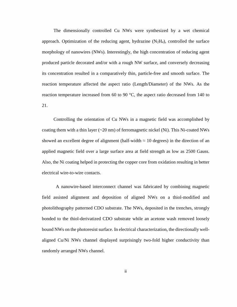
The dimensionally controlled Cu NWs were synthesized by a wet chemical
approach. Optimization of the reducing agent, hydrazine (N2H4), controlled the surface
morphology of nanowires (NWs). Interestingly, the high concentration of reducing agent
produced particle decorated and/or with a rough NW surface, and conversely decreasing
its concentration resulted in a comparatively thin, particle-free and smooth surface. The
reaction temperature affected the aspect ratio (Length/Diameter) of the NWs. As the
reaction temperature increased from 60 to 90 °C, the aspect ratio decreased from 140 to
21.
Controlling the orientation of Cu NWs in a magnetic field was accomplished by
coating them with a thin layer (~20 nm) of ferromagnetic nickel (Ni). This Ni-coated NWs
showed an excellent degree of alignment (half-width ≈ 10 degrees) in the direction of an
applied magnetic field over a large surface area at field strength as low as 2500 Gauss.
Also, the Ni coating helped in protecting the copper core from oxidation resulting in better
electrical wire-to-wire contacts.
A nanowire-based interconnect channel was fabricated by combining magnetic
field assisted alignment and deposition of aligned NWs on a thiol-modified and
photolithography patterned CDO substrate. The NWs, deposited in the trenches, strongly
bonded to the thiol-derivatized CDO substrate while an acetone wash removed loosely
bound NWs on the photoresist surface. In electrical characterization, the directionally well-
aligned Cu/Ni NWs channel displayed surprisingly two-fold higher conductivity than
randomly arranged NWs channel.

iii
DEDICATION
This dissertation is dedicated to my parents and all my family members.
iv
ACKNOWLEDGEMENTS
I would like to express my deepest gratitude towards my research advisor Dr.
Shankar B. Rananavare for his motivation, support, guidance, and encouragement during
my studies at Portland State University. I am thankful for teaching me how to approach the
difficult problems in research and allowing me to grow as a research scientist. I am blessed
to have you as my supervisor for my Ph.D. study.
I am indebted to my dissertation committee members: Dr. Robert Strongin, Dr. Dean
Atkinson, Dr. Gwen Shusterman, Dr. Andres La Rosa and Dr. Charlie Monstross for their
contributions towards completion of my degree requirements. I am also grateful to the
faculty and staff members of Chemistry Department, PSU for their support, including
uninterrupted financial support during my studies.
I would also want to thank past and current members of the Rananavare’s research
group; Dr. Nabil Mistkawi, Dr. Kayode Morakinyo, Dr. Ruchi Gakhar, Dr. Hoang Tran,
Atul Gupta, Mitra Ghobadi, Ryan Lerud, Drew Beseau, Fardowsa Idris, Patricia Monsilla,
Ana Jenike, Amanda F.Pereira, Irene R. Aguilar, Evangeline Liu and Emmanuel Abdul for
their suggestions and invaluable support. I am also grateful to the all high school interns;
Musa Tahir, Nikhil Murthy, Lauren Cooper and Vineet Edupuganti for their help in
carrying out some of my experiments and I have learned valuable supervising experience
after closely guiding them in the lab.
I want to express my sincere gratitude to Dr. Tahir Ghani, Intel for his invaluable
supervision for my thesis and career. I am also grateful to Dr. Deepak Rajput, Intel for his

v
mentorship and career guidance. Also, special thanks are due to Dr. Raj Solanki, Dr.
Andres La Rosa and their group members for their kind access and help in SEM, AFM,
and optical microscopy characterization. Finally, I also thank Tony Chen and Greg Baty,
CEMN, for their help in SEM, TEM, t-EBSD characterization work. I thank my friend
Susan Caisse for her help in editing my manuscripts and valuable friendship.
I greatly appreciate the love and support of my wife Haindhavi for being there for
me, in every way and her words of encouragement. I am indebted to my parents for their
endless support, love, and encouragement over the years and it was the greatest gift anyone
has ever given me. My profound gratitude goes to my brother Satish Rao, for his moral
support and encouragement. Finally, I give glory to the God that I believe in for giving me
faith to trust in him.

vi
TABLE OF CONTENTS
ABSTRACT.……………………………………………………….……....….….…...….i
DEDICATION…………………………………………………………………..…..…..iii
ACKNOWLEDGEMENTS……………………………………....…………….……… iv
LIST OF TABLES………………………………………………………….…….….…..x
LIST OF FIGURES………………………………………………………....…………. .xi
LIST OF SCHEMES…………………………………………………….……….….… xv
LIST OF ABBREVIATIONS…………………………………………….……...…… xvi
CHAPTER ONE: INTRODUCTION AND RATIONALE.........……………..………1
1.1. Review on traditional process of copper interconnects fabrication on chips……....2
1.2. Challenges in modern integrated circuit fabrication………………………….…... 6
1.3. Alternate materials and methods for interconnect fabrication……………….…… 7
1.4. Thesis objectives and outlines……………………………………………….…... 16
CHAPTER TWO: INSTRUMENTATION, MATERIALS AND METHODS…..….21
2.1. INSTRUMENTATION…………………………………………………….…...21
2.1.1. Fourier transform infrared spectroscopy (FTIR)……………………….….……21
2.1.2. Nuclear magnetic resonance (NMR) spectroscopy………………………..……21
2.1.3. X-ray photoelectron spectroscopy (XPS)……………………………….……...21
2.1.4. Contact angle measurements………………………………………….………..22
2.1.5. Electromagnet system……………………………………………………….….23
2.1.6. Scanning Electron Microscopy (SEM)……………………………….…….…..24
2.1.7. Transmission Electron Microscopy (TEM)……………………………..……...26
2.1.8. Optical microscopy…………………………………………………….….……27
2.2. MATERIALS AND METHODS……………………………………….………27
2.2.1. Materials used for Cu NWs synthesis, nickel electroless plating, surface
functionalization of CDO wafer and photolithography………………..….….....…….27

vii
2.2.2. Copper nanowires synthesis method……………………………….………...…28
2.2.3. Electroless coating of nickel on Cu NWs surface……………….……………...28
2.2.4. Unidirectional alignment of Cu/Ni NWs………………………….………….....29
2.2.5. Common synthetic procedure for selective functionalization of Si-OH
moieties……………………………………………………………………………….30
2.2.6. RCA cleaning procedure for SiOx and CDO wafers……………….…….……..31
2.2.7. Photolithography………….……………………………………………………32
2.2.8. Electrical characterization of self-assembled interconnect channels…….…….34
CHAPTER THREE: COPPER NANOWIRES SYNTHESIS AND MAGNETIC
FIELD ASSISTED ALIGNMENT……………………………………………….……35
3.1. Copper nanowires synthesis……………………….………………….….……….36
3.1.1. Cu NWs synthesis procedure………………………….…………..……….36
3.1.2. Effect of synthesis temperature…………………………….……..….…….39
3.1.3. Effect of reducing agent concentration……………………………..….…..41
3.2. Electroless plating of nickel (Ni) on Cu NWs surface……………..………..….…47
3.2.1. Nickel electroless plating procedure……………………….………...…….47
3.3. Magnetic field assisted alignment……………………………….…….…..….…..49
3.3.1. Effect of magnetic field strength on NWs alignment order………..….…....52
3.4. Summary of copper nanowires synthesis and magnetic field assisted
alignment…………………………………………………...........................................55
CHAPTER FOUR: SURFACE DERIVATIZATION ON CARBON DOPED
SILICON OXIDE (CDO) WAFER……………………………………………...…..…57
4.1. Introduction…………………………………………………………………..…..57
4.2. CDO as a low-k dielectric material………………………………………...…….60
4.3. Review on CDO film preparation and chemical structure……………………….61
4.4. Review on CDO damage and repairing methodologies…………………..…..….62
4.4.1. Review on CDO damage by plasma processing……………………..…....62

viii
4.4.2. Review on CDO repairing methodologies……………...…………………64
4.5. Results of developed pathway for selective derivatization of silanol………..……65
4.5.1. Developed scheme for surface derivatization……………….……….....….65
4.5.2. Results on organic molecules…………………………………….….….….66
a) tert-Butyldimethylsilanol……………………………………….....…..67
b) tert-Butyltrimethylsilane…………………………………...……….…71
c) Ethoxytriphenylsilane……………………………………...……….…72
4.5.3. Results on silica gel reaction…………………………………….………....73
4.5.4. Results on SiOx wafer reaction……………………….……………………80
4.5.5. Results on CDO wafer reaction………………………………...…….……83
4.5.6. Comparison of octadecyl chain derivatized via DIBAL-H chemistry and
octadcyltrichlorosilane (OTS) routes…………………………………………….92
4.5.7. Characterization of film dielectric constants (k)……………….…….…….93
4.6. Thiol functionalization of CDO surface to enhance NWs interaction to
substrate…………………………………………………...……………….…………98
4.7. Summary of octadecyl and thiol functionalization…………….…….…..………101
CHAPTER FIVE: NANOWIRES SELF-ASSEMBLY AND ELECTRICAL
CHARACTERIZATION………………………………………..……...…………….102
5.1. Self-assembly of Cu/Ni NWs into interconnects……………………………….102
5.2. Electrical characterization of Cu/Ni NWs based interconnects………...………104
5.2.1. Effect of nanowire type (pure Cu NWs vs. Cu/Ni NWs) and arrangement
(random vs. aligned) style on electrical performance……………………...….. 104
5.2.2. Effect of nanowires alignment order on electrical performance………....108
5.2.3. Effect of NWs density on resistance of well-aligned Cu/Ni NWs
channels………………………………………………….……………………...110
5.2.4. Thermal stability of Cu NWs and Cu/Ni NWs based interconnect
channels…………………………………………………………………………111
5.3. Summary of Cu/Ni NWs self-assembly and electrical characterization…...……113

ix
CHAPTER SIX: CONCLUSIONS AND FUTURE WORK………………..………114
6.1. Conclusions ……………………………………………………………….……114
6.2. Limitations ……………………………………………………………..……….115
6.3. Other applications …………………………………………………...…….……116
6.4. Future work……………………………………………………….……….…….117
REFERENCES ……..………………………………………………….…….……..…118
APPENDICES…………………….……………………………………….…………..132
Appendix-A. Protocol for nanowires length distribution measurement ……….….…....132
Appendix-B. Procedure for nanowires alignment angle measurement ………..…....….133
Appendix-C. Challenges in using ultra-long nanowires for the alignment………....…..134

x
LIST OF TABLES
Table 2.1. Photolithography process steps and conditions ……………………………....33
Table 3.1. Average lengths, diameters and aspect ratios of copper nanowires synthesized
at 60, 70, 80, and 90 °C respectively…………………………………………….….…….40
Table 3.2. List of field dependent parameters……………………………………………55
Table 4.1. Dielectric constant (k) values of various substances…………………………60
Table 4.2. Kinetics of contact angle results of water droplet on clean CDO and octadecyl
derivatized CDO.………………………………………………………………………....91
Table 4.3. Contact angle, film thicknesses of CDO and SiOx wafers………..….…96
xi
LIST OF FIGURES
Figure 1.1. Cross section SEM image of copper multilevel interconnect system with
CDO as a low-k dielectric…………………………………………………………………1
Figure 1.2. Schematic of DD process for making metal lines and vias…………..………4
Figure 1.3. Schematic diagram of electroplating of copper on wafer…………………….5
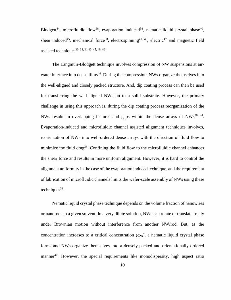
Figure 1.4. Schematic showing various kinds of nanowires self-assembly………..………9
Figure 1.5. Schematic diagram showing shear force induced self-assembly of NWs…...13
Figure 1.6. Schematic illustrating electric field assisted alignment of NWs………....….14
Figure 1.7. Schematic diagram illustrating the process of magnetic field assisted assembly
of magnetically active nanowires……...………..………………………………….…….15
Figure 1.8. Schematic diagram illustrating the Cu/Ni NWs self-assembly………………16
Figure 1.9. Schematic diagram showing process flow of Cu/Ni NWs self-assembly into
interconnect channels…………………………………...………………………………..20
Figure 2.1. Water contact angle measurement setup….………………………..…..….…23
Figure 2.2. Plot showing change in magnetic field strength as a function of applied
magnetic field strength………………………………………………………………..….24
Figure 2.3. Schematic diagrams illustrating the difference between EBSD and t-EBSD
processes of crystallographic orientation mapping in SEM………………………………25
Figure 2.4. Digital photographs showing custom-made sample holder for TKD data
collection of Cu NWs ………………………………………………………………...….26
Figure 2.5. Digital photographs of GMW electromagnet setup …………………..…..…30
Figure 2.6. Schematic diagram showing photolithography process flow……..……….…32
Figure 2.7. Digital photograph showing projection mask UV aligner……………....……34
Figure 3.1. Digital images of Cu NWs reaction solution before adding hydrazine (a), after
adding hydrazine (b), and after incubation for 30 minutes in hot water bath……………...37
Figure 3.2. SEM images of copper nanowires synthesized at 60 °C (a), 70 °C (b), 80 °C
(c), and 90 °C (d) respectively……………………………………………………...…….40

xii
Figure 3.3. SEM images of Cu NWs synthesized using high concentration (35 µL) of
reducing agent……………………………………………………………………………41
Figure 3.4. SEM images of copper nanowires synthesized using an intermediate
concentration of hydrazine (8.28x10⁻³M, 30 µL)…………………………………………42
Figure 3.5. SEM images of Cu NWs synthesized using low concentration of reducing agent
shown at low a) and high b) magnification scales…………………………….…..………44
Figure 3.6. TEM image of Cu NW synthesized using 5.73x10⁻³M (21 µL) concentration
of hydrazine highlighting the particle-free surface…...…………………………………..45
Figure 3.7. Low magnification bright field a), and high magnification dark field b), TEM
image showing the presence of nanoparticles…………………………………………….47
Figure 3.8. Digital photographs showing nickel electroless plating setup and magnetic
response of Cu/Ni NWs towards neodymium disc magnets……………………...………48
Figure 3.9. SEM image of nickel coated copper nanowire a) and elemental mapping
showing distribution of copper core and nickel coating on the surface……………….…49
Figure 3.10. Digital photographs of electromagnet setup………………………….……49
Figure 3.11. Optical microscope images of Cu/Ni NWs orientation in absence (a), and in
the presence of applied magnetic field (2500 Gauss) (b)....................................................52
Figure 3.12. Optical micrographs showing alignment order of Cu/Ni NWs at various
applied magnetic field strength from 0 G to 2500 G…………………….……….………53
Figure 3.13. Plot showing average NWs alignment angle with respect to the applied
magnetic field direction, at various field strength from 0 G to 2500 G……………..……54
Figure 3.14. Gaussian peak fitting plots showing NWs alignment distribution with respect
to the applied magnetic field strength from 0 to 2500 Gauss……………………....…….54
Figure 4.1. Image of multilayered integrated circuit (IC) using Cu/W/ SiO2 dielectric
materials, developed by IBM in 1997…………………………………………...…….….59
Figure 4.2. a) Chemical structure of porous cage networked structure of as-prepared CDO
film from TMCTS precursor…………………………………………...………..……….63
Figure 4.3. 1H-NMR (C6D6, 400 MHz) reaction progress study of TBDMS Triflate
synthesis at 2, 24, 48 and 72 hours respectively…………………………………………..69
Figure 4.4. 1H-NMR (CDCl3, 400 MHz) reaction progress study of tert-
Butyldimethylsilane synthesis at 2, 24, 48 and 72 hours respectively…………….………70
xiii
Figure 4.5. 19F-NMR (CDCl3, 400 MHz) reaction progress study of tert-
Butyldimethylsilane synthesis at 2, 24 and 48 hours respectively…………………….…..71
Figure 4.6. 1H-NMR (DMSO-d6) reaction progress study of tert-Butyltrimethylsilane
synthesis at 2, 24 hours of reaction………………………………………………….……72
Figure 4.7. 1H-NMR (DMSO– D6) of triphenylsilane synthesis reaction………………..73
Figure 4.8. Experimental setup of silica gel reaction …………….……….……........…...75
Figure 4.9. FTIR spectra of silica gel in various stages of reaction.……………..…….…76
Figure 4.10. 19F NMR study of silica gel reaction with triflic anhydride…………........…78
Figure 4.11. FTIR of silica gel control experiment. Comparison of pure silica gel before
reaction and after treatment with 1-octadecene in the presence of UV light………..……..80
Figure 4.12. FT-IR spectra of SiOx wafer at various stages of the reaction…….…81
Figure 4.13. Common reaction pathway for hydrogen termination, octadecane
derivatization and experimental setup of carbon doped silicon oxide (CDO) wafer….…..83
Figure 4.14. FT-IR spectra of CDO wafer in various stages of reaction………….………84
Figure 4.15. Control experiment showing that only the porous structure of CDO traps
DIBAL-H from anhydrous toluene solution……………………………..………….……87
Figure 4.16. FTIR of CDO wafer control experiment. Spectral comparison of clean CDO
before reaction and CDO after treatment with 1-octadecene…………………………..…89
Figure 4.17. XPS spectra of CDO wafer. Survey spectrum and high-resolution spectrums
of Si (2p) collected before the reaction…………………………….………………….….90
Figure 4.18. Water contact angles measured on un-derivatized (clean CDO) and
octadecene derivatized CDO wafers at various time intervals……….……….………..…91
Figure 4.19. FTIR spectra comparison of octadecyl derivatized CDO wafer before and
after one-year duration……………………………………………………..…….………92
Figure 4.20. Comparison CDO and SiOx wafer derivatized by DIBAL-H assisted
chemistry (blue) vs. OTS chemistry (red)…………………………….…………….……93
Figure 4.21. Capacitance vs. voltage curves measured using Hg probe method. Hg contact
area was 3.1x10⁻³ cm2……………………………………………………………….……94
Figure 4.22. FTIR characterization of as received CDO (black curve) and thiol (-SH)
functionalized CDO (red curve) ………………………………………………….………99

xiv
Figure 4.23. Digital photograph showing ultrasonication setup (a), for qualitatively testing
the adhesion strength of Cu/Ni NWs to as received CDO and thiol modified CDO……100
Figure 5.1. Schematic diagram showing process flow of Cu/Ni NWs self-assembly into
interconnects………………………………………………………………………….…………104
Figure 5.2. Optical micrographs of unidirectionally aligned Cu/Ni NWs interconnect channel
fabricated depositing 0.5 mg/mL of NWs solution………………….……………………..……104
Figure 5.3. Schematic diagrams and digital photographs showing interconnect channels
fabricated using different types and arrangement styles of NWs…………….….………105
Figure 5.4. Optical micrographs of Cu NWs based interconnect channel at various
magnification scales showing the random arrangement of Cu NWs…………..…...……106
Figure 5.5. Optical micrographs of Cu/Ni NWs based interconnect channel at various
magnification scales showing directionally well-arranged NWs…………………..……106
Figure 5.6. Optical micrographs of Cu/Ni NWs based interconnect channel at various
magnification scales showing randomly arranged NWs…………………………...……107
Figure 5.7. Plot showing resistance values of well-aligned and randomly arranged Cu/Ni
NWs and randomly arranged pure Cu NWs based interconnect channels…...…..………107
Figure 5.8. Schematic depicting systematic alignment of bar magnets in presence of
applied magnetic field and random alignment in absence of magnetic field……..…..…108
Figure 5.9. Optical microscope images of interconnect channels fabricated at various
applied magnetic field strength from 0 to 2500 Gauss………………………..…………109
Figure 5.10. Plot showing resistance values of Cu/Ni NWs based interconnect channels
fabricated using various applied magnetic field strength from 0 to 2500 G…………..…110
Figure 5.11. Low and high magnification optical micrographs showing of interconnect
channels fabricated by using 0.5 mg/mL, 1.0 mg/mL and 2 mg/mL respectively…….…111
Figure 5.12. Resistance values of Cu/Ni NWs based interconnect channels prepared using
various concentrations of Cu/Ni NWs solutions………………………………...………111
Figure 5.13. Thermal stability of well-aligned and randomly arranged Cu/Ni NWs
channels and randomly aligned Cu/Ni NWs channels at 100 °C in air………...…….…112

xv
LIST OF SCHEMES
Scheme 1.1. Schematic representing selective functionalization of surface exposed Si-OH
functional groups to thiol-derivatized silicon……………………………...……………..19
Scheme 2.1. Schematic of common reaction pathway for selective functionalization of Si-
OH functional groups to Octadecyl and thiol-derivatized silicon……………….…….….31
Scheme 4.1. Schematic of the new reaction pathway for hydrogen termination and
octadecane (Si-R, R= C18H37) derivatization………………………………….…….……65
Scheme 4.2. Schematics of various compounds considered for testing surface
derivatization reaction……………………………………………………………………66
Scheme 4.3. Schemes of a) Synthesis of TBDMS Triflate and tert-Butyldimethylsilane, b)
Synthesis of tert-Butyltrimethylsilane c) Synthesis of Triphenylsilane…………….……67
Scheme 4.4. Reaction scheme describing thiol functionalization of CDO surface…….…98
xvi
LIST OF ABBREVIATIONS
Abbreviation Meaning
Cu NWs
Cu/Ni NWs
SEM
TEM
Copper nanowires
Nickel coated copper nanowires
Scanning Electron Microscopy
Transmission Electron Microscopy
CA Contact angle
DI Deionized
t-EBSD Transmitted electron backscattered diffraction
EBSD Electron backscattered diffraction
CDO Carbon doped silicon dioxide
CMP Chemical mechanical polishing
DD Dual Damascene
EM Electromigration
PET Polyethylenetetrapthalate
DB Diffusion barrier layer
IC Integrated circuits
RC Resistance and capacitance
FTIR Fourier transform infrared spectroscopy
XPS X-ray photoelectron spectroscopy
XRD X-ray diffraction spectroscopy
EDS/EDX Energy dispersive X-ray spectrum
EDA Ethylenediamine
PECVD Plasma enhanced chemical vapor deposition
OTS Octadecyltrichlorosilane
DIBAL-H Di isobutyl aluminum hydride

1
CHAPTER ONE
INTRODUCTION AND RATIONALE
Copper is one of the oldest and the third most industrially consumed metal. It has
received a great deal of attention for its wide variety of applications, such as electrical
conductor in electronics, architecture, plumbing, human health, and many other consumer
products1. Copper has been the wiring metal of choice in electronic devices because of its
ductility, malleability and excellent conductivity characteristics. Especially in chip
fabrication, copper is being used as an interconnect material which plays an important role
in the power supply and electric signal distribution2.
Figure 1.1. Cross section SEM image of copper multilevel interconnect system with CDO as a
low-k dielectric3 insulator.
In 1997, IBM revolutionized the technology industry with its remarkable innovation
of chips made of copper interconnects. Replacing the traditional aluminum with copper as
an interconnect material, enabled smaller chip sizes, cheaper production, and faster
2
performance4-6. Today, in the current ultra large-scale integration (ULSI) technology
copper (Cu) and tungsten (W) are being used as interconnect materials. Tungsten is used
for ground level interconnects which communicates to the transistors. Copper is being used
for all other layers, which can have as many as 12 metallic interconnect levels. Copper
metal lines in each level communicate to other levels through copper vias as shown in
Figure 1.1.
Ultra large scale integrated (ULSI) circuit device manufacturing technology can be
divided into two main stages. The first stage is transistor and its other component structures
fabrication. At the second stage, huge numbers of transistors are connected to each other
by three-dimensional multilayers of copper interconnect systems3, 7. Transistors are the
active components of a chip and are where signals are controlled and generated. Each
transistor communicates to other active parts of a chip through electric signals that are
carried by highly complex copper interconnect systems. Ultimate speed limit and chip
performance are determined by the frequency at which transistors can turn on and off 8.
Since clock frequency increases with decreasing transistor size, advances in chip speeds
have been achieved by shrinking the feature sizes and increasing the count. Currently, the
speed limit and performance of a chip is set by signal propagation delays and the time
constant of the copper interconnects9.
1.1. Review on traditional process of copper interconnects fabrication on
chips
All metal lines and vias of integrated circuits (ICs) are fabricated by an industrially
standard Dual Damascene (DD) process2. DD involves defining the line and via pattern in
3
a dielectric using photolithography technique and backfilling the opening with copper by
an electrochemical method. Finally, the excess copper removed by chemical mechanical
planarization (CMP) process2, 10.
Dual Damascene (DD) process
The Damascene process was initially developed for jewelry manufacturing2. In a
single Damascene process trenches and vias are filled with copper in two separate steps. In
Dual Damascene (DD) process trench and vias are filled in a single step. In comparison to
single Damascene, DD process lowered the number of processing steps and became the
industrially standard interconnect fabrication technique. The advantage of this method is
super filling, which results in a void-free and seamless filling of high aspect ratio trenches
and vias10.
In advanced IC integration, single Damascene is only used for Tungsten (W) local
interconnects and all other copper interconnects are made by using Dual Damascene
process. All high-density metal lines and vias are insulated by an inner layer dielectric
(ILD) material. Copper is known to be a fast diffuser into silicon and its oxide dielectrics.
This causes deep level defects which may lead to poor performance or chip failure. By
using a Ti, TiN, Ta or TaN as a diffusion barrier, one can localize copper to where it is
desired2.
4
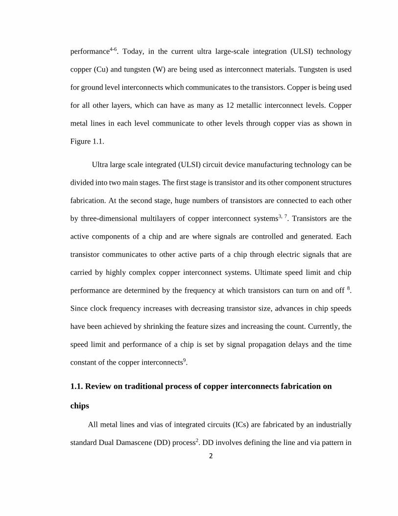
Figure 1.2. Schematic of DD process for making metal lines and vias. The process involves
diffusion barrier layer (DB) deposition, copper seed layer deposition (CSL), copper filling by
electroplating process and removal of excess copper by a chemical mechanical planarization
process (CMP)2.
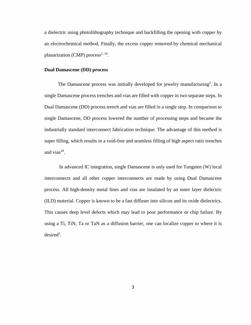
Major steps involved in DD process are illustrated in Figure 1.2. The DD process
starts with depositing a thin layer of a diffusion barrier (DB) layer (Ta, TaN) commonly
done by ionized metal plasma (IMP) method. It is followed by depositing a thin copper
seed layer (CSL), usually by sputtering. Copper electroplating method emerged as the most
promising and commercial viable technique for copper filling8. A schematic of
electrochemical deposition set up is shown in Figure 1.38. CSL coated wafer is then
immersed in an electroplating solution and electrically connected and acts as a cathode.
Copper sulfate (CuSO4) and sulfuric acid (H2SO4) are the common components of

5
electrolytes. Cupric ions (Cu2+) from an electrolyte solution get reduced and deposited on
CSL surface which results in super filling of trenches and vias.
Figure 1.3. Schematic diagram of electroplating of copper on the copper seed layer (CSL) coated
wafer8.
After trenches and vias are filled with copper, the excess copper is removed by
Chemical Mechanical Polishing (CMP). In CMP process, polishing with a slurry removes
excess copper by the combination of chemical reactivity and mechanical abrasion2, 10.
Chemicals in the slurry react with copper and typically form copper oxides and are
subsequently removed by mechanical abrasion. After polishing for an optimum period, the
wafer surface becomes planar. Capping of Cu interconnects by silicon nitride, or silicon
carbide (known as Etch Stop (ES) layer) completes one level of interconnect fabrication.
All these above discussed processes will be repeated for multiple times for the fabrication
of multilayered highly complex Cu interconnects.

6
1.2. Challenges in modern integrated circuits fabrication
Today, modern chips use several billion of transistors and other electronic
components in an area of about 1 cm2 11. As the transistor count increasing, copper wire
dimensions are shrinking to nanometer scales to connect these individual transistors.
With the ever-decreasing copper wire dimensions, the resistance of the narrow
conductive channel is increasing due to electron scattering by the grain boundaries and at
wire surfaces. Increased resistance adversely contributes to the overall signal propagation
delay. In the modern chips, total resistance (R) of the copper interconnect structure is a
significant factor that affects the chips performance9, 11. Furthermore, as the area of copper
interconnects increase, the capacitance (C) between the closely squeezed conductive
channels also increases. Both effects significantly increase in the RC signal delay, which
results in degraded performance of the chips9. Hence, in recent years enormous efforts have
been devoted to developing new process technologies to fabricate miniaturized crystalline
copper interconnects and to prepare low-k insulators to minimize the capacitance (C) and
leakage current.
In the narrow copper wires, mechanical stress and current density significantly
increase (>2 MA/cm2) which ultimately leads to electromigration (EM) related
interconnect failures12, 13. High current density in the narrow metal lines causes void
nucleation, propagation along the metal lines and creates cracks14. Electromigration failure
mechanisms have been discussed in detail elsewhere13, 15, 16. Also, the standard DD process
requires deposition of diffusion barrier and copper seed layers in the narrow trenches and
vias. But, as the feature sizes are shrinking to few nanometer scales, it is becoming very
7
challenging to have these layers and fill them with copper. Ultimately, the fabrication of
interconnects in a DD process is reaching its fundamental limits. Therefore, innovative
materials and process solutions are very critical to sustaining the miniaturization and
performance trends.
1.3. Alternate materials and methods for interconnect fabrication
In the recent history, bottom-up or hybrid approaches of nanoscale circuit fabrication
using nanomaterials as building blocks, have received considerable attention17-19. This kind
of bottom-up approach of integrated circuit fabrication involves the synthesis of
nanocrystals with desired physical and electrical properties and their self-assembly into
electronic circuits19.
Desirable material properties for the fabrication of interconnects:
As the DD processed on-chip copper wire dimensions are reaching to nanoscales,
they experience two principal issues. First, electron scattering induced degradation of
electrical resistivity. Second, their reliability issues due to poor electromigration (EM)
resistance17. In addition to the above two issues, oxidation under ambient conditions and
enhanced oxidation at high resistive self-heating are also the major growing concerns20.
The ideal building blocks used for the interconnect fabrication should possess high
conductivity, excellent electromigration (EM) resistance, high oxidation resistance and
economical20. Therefore, a quest for alternate interconnect materials which address the
above issues have been under active search.

8
Promising building blocks for the fabrication of interconnects:
Nanomaterials show significantly improved electrical, mechanical and thermal
properties compared to their bulk material counterparts. Especially 1D nanomaterials, such
as pure metallic nanowires, core-shell nanowires and carbon nanotubes (CNT), etc., are
very attractive building blocks for functional nanoscale electronic devices, owing to its
unique anisotropic structure-dependent properties. Assembly of 1D nanomaterials in a
bottom-up or hybrid approach offers an excellent alternative for the fabrication of
miniaturized and high-performance interconnects17, 20-28. Many kinds of 1D nanomaterials
such as pure metallic (Cu17, 29, Ag20, Au25, Pt30) NWs, core-shell NWs (Graphene
encapsulated Cu NWs31) and carbon nanotubes32 (CNT), etc., have been explored as
promising building blocks for interconnects17, 20-28.
Among all 1D nanomaterials, copper nanowires (Cu NWs) have attracted
considerable interest in recent years due to their intriguing electrical, thermal and
mechanical properties17, 18, 33. Copper has the second highest electrical conductivity among
metals, highly abundant and low cost. Thus Cu NWs have been considered as promising
building blocks for many applications, such as flexible & transparent electrodes33-35,
conductive inks18, catalyst36 and interconnects17. Also, copper is successfully being used
as an interconnect material on-chip since 199737. Therefore, Cu NWs are the ideal
candidates for many micro and functional nanoscale devices, and it is imperative to develop
a simple and reliable technique to assemble the Cu NWs into a functional device.

9
Review of NW self-assembly techniques:
Self-assembly refers to the process in which nanowires or other discrete components
spontaneously organize into ordered macroscopic structures owing to its direct specific
interactions (e.g., interparticle forces), or indirectly using an externally applied field30, 38,
39. The essential feature of nanowire self-assembly is an organization of NWs in an
orientationally and positionally well-ordered manner30, 40.
Figure 1.4. Schematic describing various kinds of nanowires self-assembly techniques that
arranges disordered NWs into well-ordered manner41.
In a bottom-up or hybrid approach, precisely controlling the NWs orientation and
positioning are the first critical steps for the successful assembly of individual NWs into a
functional nanodevice38, 42, 43. Several approaches for controlling the orientation of NWs
via a self-assembly process have been studied (See Figure 1.4), such as Langmuir-
10
Blodgett44, microfluidic flow38, evaporation induced38, nematic liquid crystal phase40,
shear induced45, mechanical force38, electrospinning41, 46, electric47 and magnetic field
assisted techniques30, 38, 41-43, 45, 48, 49.
The Langmuir-Blodgett technique involves compression of NW suspensions at air-
water interface into dense films44. During the compression, NWs organize themselves into
the well-aligned and closely packed structure. And, dip coating process can then be used
for transferring the well-aligned NWs on to a solid substrate. However, the primary
challenge in using this approach is, during the dip coating process reorganization of the
NWs results in overlapping features and gaps within the dense arrays of NWs38, 44.
Evaporation-induced and microfluidic channel assisted alignment techniques involves,
reorientation of NWs into well-ordered dense arrays with the direction of fluid flow to
minimize the fluid drag38. Confining the fluid flow to the microfluidic channel enhances
the shear force and results in more uniform alignment. However, it is hard to control the
alignment uniformity in the case of the evaporation induced technique, and the requirement
of fabrication of microfluidic channels limits the wafer-scale assembly of NWs using these
techniques38.
Nematic liquid crystal phase technique depends on the volume fraction of nanowires
or nanorods in a given solvent. In a very dilute solution, NWs can rotate or translate freely
under Brownian motion without interference from another NW/rod. But, as the
concentration increases to a critical concentration ( N), a nematic liquid crystal phase
forms and NWs organize themselves into a densely packed and orientationally ordered
manner40. However, the special requirements like monodispersity, high aspect ratio

11
nanowires and that NWs should not precipitate out from the solution, etc. limits this
technique.
Shear force or mechanical force induced reorganization of NWs is one of the large-
scale assembly techniques38, 45. Here, a shear force is created by the motion of a solid object
or fluid against a second solid object or fluid. In either case, a force is generated parallel to
the sliding direction and aligns the NWs in the direction of movement. This technique is
inexpensive and can be applied to various substrates such as Si wafers and flexible or
curved substrates. However, this process requires excellent skills and the challenging thing
in this technique is controlling the viscosity of the NWs solution 38.
Electrospinning is a versatile technique, using electrostatic forces to form continuous
chains of fibers, polymers or nanowires. In a typical electrospinning technique, NWs or a
polymer suspension pumped through a thin nozzle with an inner diameter of ~100 µm41, 46.
And, the nozzle simultaneously serves as an electrode, to which high electric field of 100-
150 kV m-1 is applied. While the NWs solution is passing through the nozzle, under the
influence of the strong electrostatic field, assembly of electrospinning fibers along the axial
directions occurs. Very complex experimental setup and the requirement of high voltages
are limits to the usefulness of this technique.
In the case of electric field assisted alignment technique, highly polarizable NWs
polarize readily in the alternating electric field due to charge separation at the NWs surface
and will experience the dielectrophoretic force that produces net movement to the NWs47.
However, NWs at various locations in between the electrodes experience an unequal
dielectrophoretic force which results in poor alignment in the center regions and excellent
12
alignment in the regions close to the electrodes. However, the requirement of electrode
fabrication for the NWs alignment and it is only applicable to the polarizable materials
(e.g., CdSe, ZnO, Se NWs), etc., limits this technique to implementation for large-scale
assembly processes.
Finally, the magnetic field assisted technique involves applying of an external
magnetic field to directionally organize the magnetically active nanowires suspended in
the solution30, 38, 41-43, 45, 48-50. In the presence of an applied magnetic field, each NW will
polarize into north and south poles and orient themselves parallel to the applied magnetic
field direction30, 51. The uniformity of the NWs alignment depends on the applied magnetic
field strength. The added advantage of this technique is the assembled NWs forms chain-
like structures by connecting each NW in a head to tail fashion, which gives a continuous
network of NWs. These kinds of continuous networks are ideal for the best electrical
performance. However, the main drawback of this technique is, it can only be applied to
magnetically active NWs.
Review on using nanowires self-assembly techniques to build functional nanodevices:
The number of nanodevices, such as interconnects, FETs, bipolar transistors, light emitting
diodes (LED) and logic gates have been assembled in a bottom-up approach from well-
defined nanowires17, 29, 30. Here discussed are few NWs self-assembly techniques used for
assembling the NWs into functional devices.

13
Figure 1.5. Schematic diagram showing shear force induced self-assembly of Ge NWs into
photolithography patterned channels (a), and optical micrographs of crossed arrays of Ge NWs
shown at low (b) and high (c) magnifications. SEM images of single and multiple Ge NWs
assembled into FET device (d)38, 52.
Figure 1.5 depicts the shear force assisted NWs self-assembly into crossed arrays
and field effect transistor (FET) device. This process involves, mechanical movement of a
donor substrate consisting of a lawn of vertically grown NWs, onto a photolithography
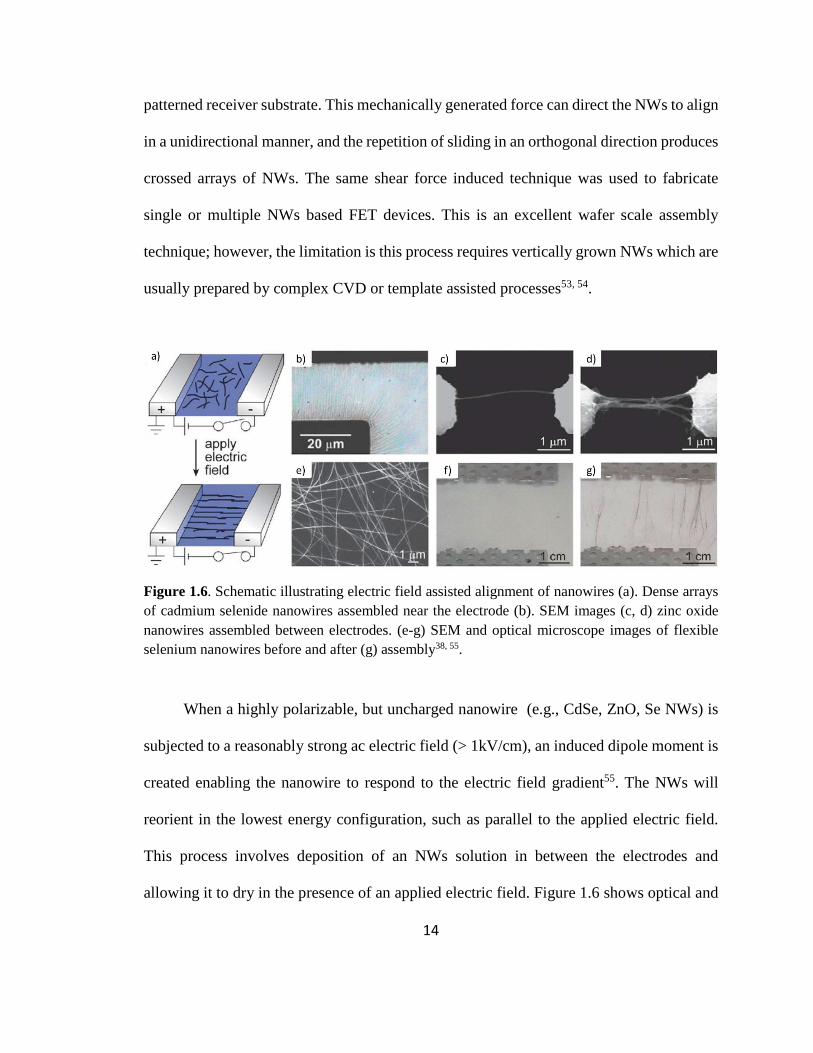
14
patterned receiver substrate. This mechanically generated force can direct the NWs to align
in a unidirectional manner, and the repetition of sliding in an orthogonal direction produces
crossed arrays of NWs. The same shear force induced technique was used to fabricate
single or multiple NWs based FET devices. This is an excellent wafer scale assembly
technique; however, the limitation is this process requires vertically grown NWs which are
usually prepared by complex CVD or template assisted processes53, 54.
Figure 1.6. Schematic illustrating electric field assisted alignment of nanowires (a). Dense arrays
of cadmium selenide nanowires assembled near the electrode (b). SEM images (c, d) zinc oxide
nanowires assembled between electrodes. (e-g) SEM and optical microscope images of flexible
selenium nanowires before and after (g) assembly38, 55.
When a highly polarizable, but uncharged nanowire (e.g., CdSe, ZnO, Se NWs) is
subjected to a reasonably strong ac electric field (> 1kV/cm), an induced dipole moment is
created enabling the nanowire to respond to the electric field gradient55. The NWs will
reorient in the lowest energy configuration, such as parallel to the applied electric field.
This process involves deposition of an NWs solution in between the electrodes and
allowing it to dry in the presence of an applied electric field. Figure 1.6 shows optical and

15
SEM images of self-assembled nanowires near or in between the electrodes. However, this
process is only applicable to polarizable NWs, and requirements such as microelectrode
fabrication and high voltage limits this technique.
Figure 1.7. Schematic diagram illustrating the process of magnetic field assisted assembly of nickel
(Ni) NW interconnect on Ni electrodes (a). SEM image of as-fabricated Ni NW based interconnect
(b)56. Optical microscope images of Ni/Au/Ni NWs based interconnects51.
Several efforts have been devoted to the magnetic field assisted self-assembly of
magnetically active nanowires40-42, 44, 47, 48. The magnetic field assisted self-assembly
involves directed deposition of well-aligned NWs on the electrodes. This process involves
deposition of suspension of a magnetically active NWs solution on substrate and drying of
the solution in the presence of applied magnetic field like the schematic shown in Figure
1.7. In the solution, the NWs align in the applied magnetic field direction, and the
orientationally aligned NWs settles down on the electrodes50, 56. Self-assembly of single
and multiple NWs based interconnects have been fabricated using pure Ni NWs56,

16
Ni/Au/Ni NWs51, Au/Ni/Au50 nanowires. However, to date, the magnetic field assisted
self-assembly technique is limited to assemble the single or few NWs into a nanodevice
but, assembly of NWs on a large-scale has not yet been demonstrated.
This thesis work describes an investigation of magnetic field assisted self-assembly
of high aspect ratio nickel coated copper nanowires (Cu/Ni NWs) into photolithography
patterned channels on a large-scale area.
1.4. Thesis objectives and outlines
The overall objective of the thesis is to self-assemble one-dimensional (1D) nanocrystal-
based interconnects. The central hypothesis of the project is “interconnects on IC surfaces
can be self-assembled.” This hypothesis was tested by developing a magnetic field
assisted technique to self-assemble the Cu/Ni NWs into photolithography patterned
channels on the large-scale area on a carbon doped silicon dioxide (CDO) wafer, like the
figure shown in Figure 1.8.
Figure 1.8. Schematic representing self-assembly of Cu/Ni NWs into photolithography patterned
channels on CDO wafer.

17
Nanowires self-assembly was achieved via three specific aims. Aim #1 is Cu NWs
synthesis and electroless coating of nickel onto the Cu NWs surface. Aim #2 is a
preparation of the CDO surface to accept nickel coated copper nanowires (Cu/Ni NWs).
Aim #3 is magnetic field assisted self-assembly and deposition of NWs into
photolithography patterned channels.
Aim #1: Cu NWs synthesis and electroless coating of nickel onto the Cu NWs surface:
In the fabrication of future bottom-up nanotechnology, the synthesis of copper
nanowires (Cu NWs) has received considerable attention in recent years, and a number of
methods have been successfully demonstrated which include template assisted processes26,
chemical vapor depositions53, hydrothermal/solvothermal routes57, and solution-based
methods33, 35, 58. Among all the available synthesis routes, the solution-based approach is
very attractive due to its process simplicity, low cost and easy to scale up for bulk scale
production58. However, a thorough understanding of the effect of reagent concentrations
and synthesis conditions on the morphology, shape and aspect ratio of NWs are very
critical. This study focuses on the effect of reducing agent concentration and synthesis
temperature on the resulting surface morphology and aspect ratio of Cu NWs. The optimum
reagent conditions to synthesize high aspect ratio Cu NWs with a smooth surface are to be
established.
Although applications of Cu NWs have been demonstrated in a wide range of devices
(e.g., transparent and flexible electrodes and conductive ink, etc.), oxidation of pure copper
into copper oxides limit its reliable performance59. Also, very limited success has been
achieved in controlling the orientation and positioning of Cu NWs, which is very critical

18
for assembly of these NWs into complex functional devices. The above two challenges are
addressed by coating a thin layer of oxidation resistant and ferromagnetic nickel onto the
Cu NWs surface in an electroless coating approach. Nickel coating helped in protecting the
copper core from oxidation and gave the magnetic response to Cu NWs. The orientation of
Cu/Ni NWs is controlled by applying the uniform magnetic field to the NWs solution
deposited onto the CDO surface.
Aim #2: Preparation of CDO surface to accept nickel coated copper nanowires (Cu/Ni
NWs).
CDO is a low-k dielectric material composed of Si, C, O, H elements and contains
surface exposed hydrophilic Si-OH functional groups. A CDO material is chosen to
demonstrate the NWs self-assembly process 60-62. Modern interconnects utilize this
material to separate copper wiring in interconnects. It is well known that thiol (-SH)
functional groups show strong interaction towards copper and nickel. Therefore, this work
uses a thiol-functionalized CDO surface to attract and hold the Cu/Ni NWs strongly after
deposition. Thiol functionalization of a CDO surface is achieved via a novel reaction
scheme developed to selectively functionalize the surface exposed Si-OH functional
groups to thiol-terminated alkyl groups, deploying the scheme shown in Scheme 1.1. The
reaction process involves the conversion of hydrophilic Si-OH functional groups to its
triflate ester (Si-O-Tf), and it is followed by reduction to hydrogen-terminated silicon (Si-
H) using DIBAL-H reagent. Finally, hydrosilylation of Si-H using 2-propene thiol
generates the thiol-functionalized CDO surface.
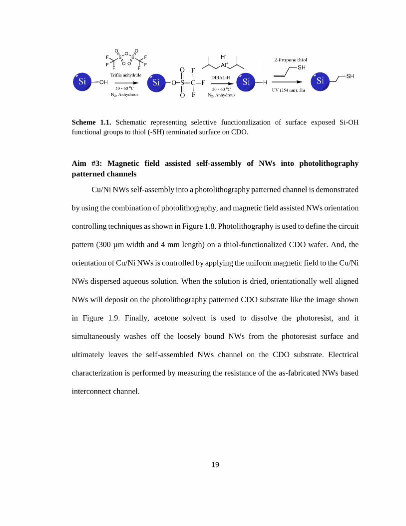
19
Scheme 1.1. Schematic representing selective functionalization of surface exposed Si-OH
functional groups to thiol (-SH) terminated surface on CDO.
Aim #3: Magnetic field assisted self-assembly of NWs into photolithography
patterned channels
Cu/Ni NWs self-assembly into a photolithography patterned channel is demonstrated
by using the combination of photolithography, and magnetic field assisted NWs orientation
controlling techniques as shown in Figure 1.8. Photolithography is used to define the circuit
pattern (300 µm width and 4 mm length) on a thiol-functionalized CDO wafer. And, the
orientation of Cu/Ni NWs is controlled by applying the uniform magnetic field to the Cu/Ni
NWs dispersed aqueous solution. When the solution is dried, orientationally well aligned
NWs will deposit on the photolithography patterned CDO substrate like the image shown
in Figure 1.9. Finally, acetone solvent is used to dissolve the photoresist, and it
simultaneously washes off the loosely bound NWs from the photoresist surface and
ultimately leaves the self-assembled NWs channel on the CDO substrate. Electrical
characterization is performed by measuring the resistance of the as-fabricated NWs based
interconnect channel.

20
Figure 1.9. Schematic diagram showing a process flow of Cu/Ni NWs self-assembly into
interconnect channels.
Thesis Outlines:
The following chapters provide the detailed information about results collected to
support the above-discussed hypothesis. Chapter-2 discusses instrumentation, materials,
and synthesis methods used in this study. The results of copper nanowires synthesis, an
electroless coating of nickel onto Cu NWs surface and magnetic field assisted NWs
orientation controlling technique details are discussed in Chapter-3. Selective
functionalization of surface exposed hydrophilic Si-OH functional groups to thiol (-SH)
terminated surface results are discussed in Chapter-4. And, Cu/Ni NWs self-assembly into
photolithography patterned channels and electrical characterization results are discussed in
Chapter-5. The thesis concludes with the discussion of summary, limitations, other
applications and future scope of the developed techniques in Chapter-6.

21
CHAPTER TWO
INSTRUMENTATION, MATERIALS AND METHODS
2.1. INSTRUMENTATION
2.1.1. FTIR Spectroscopy
Structural and functional group information on Silica gel, SiOx, and CDO substrates
were studied by Fourier transform infrared (FTIR) spectroscopy. The infrared spectrum is
a nondestructive and powerful identification tool for functional groups in a wide range of
samples (liquid, gel, solid substrates). FTIR data was collected on Thermoscientific,
NicoletTM FTIR Spectrometer, in transmittance mode from 400 to 4000 cm-1 at a resolution
of 4 cm-1. For collecting FT-IR spectra of silica gel samples, a small amount of sample (~
5 wt%) was mixed with KBr salt and pressed into a thin pellet. CDO or SiOx wafers
(dimension 1x2 cm) were directly placed in the path of IR beam and spectra collected in
transmission mode.
2.1.2. NMR Spectroscopy
Nuclear magnetic resonance (NMR) spectroscopy was used in structural
characterization and reaction progress study of organic model compounds. 1H and 19F-
NMR spectra were collected on a 400 MHz Bruker NMR instrument at 256 scans. Reaction
mixtures were dissolved in C6D6 or DMSO-d6 or CDCl3 solvents. In all discussed reactions
percentage yields were calculated from 1H or 19F-NMR spectra of crude mixtures.
2.1.3. X-ray Photoelectron Spectroscopy (XPS)

22
Surface chemical composition and bonding information were investigated using
XPS. It is a qualitative and quantitative technique for analyzing surface chemistry of
materials with extremely high sensitivity. XPS spectra were acquired on PHI Versa Probe
II Scanning XPS equipped with Argon (Ar), C60 sputtering gun and dual charge neutralizer.
Survey spectrums were collected at 187.85 eV pass energy, 1 eV/step, 20 ms per step, 5
cycles and 5 sweeps. And, high-resolution spectra were collected at 23.5 eV pass energy,
0.1 eV/step, 20 ms per step, 5 cycles and 5 sweeps. PHI MultiPak data reduction program
was used for the deconvolution and analysis of raw XPS data.
2.1.4. Contact angle measurements
The contact angle (CA) refers to the angle where a liquid droplet interacts with a flat
and horizontal solid surface. It quantifies the wettability of the surface by the liquid droplet.
A low contact angle (flat droplet) for a water drop indicates that the surface has high
wettability (hydrophilic) and a high contact angle indicates the poor wettability
(hydrophobic), see Figure 2.1b.
Water contact angle data was collected in a laboratory fabricated setup, like the
schematic and digital photograph shown in Figure 2.1 a & c. For the data collection, a PC
connected to a Kodak MDS 100 CCD camera was used to capture the droplet images on
the surface of a wafer substrate. The contact angle data was analyzed by using Image-J
software application (freeware available from NIH).
23
Figure 2.1. Schematic diagram depicting water contact angle measurement set up shown in a), and
definition of the hydrophilic and hydrophobic surface shown in image b). Digital photograph in c),
shows the laboratory fabricated CA measurement setup.
2.1.5. Electromagnet system
Unidirectional alignment of nickel coated copper nanowires (Cu/Ni NWs),
experiments were carried out by applying a uniform magnetic field in electromagnet
system, see Figure 2.2 a & b. GMW electromagnet system, Model-3470 with the
dimensions of 45 and 30 mm of the pole diameter and pole gap respectively was used.
Magnetic field strength can be varied by changing the current through magnet coil, Figure
2.2 c.

24
Figure 2.2. a) and b) showing digital photographs of electromagnet setup used for magnetic field
assisted alignment of Cu/Ni NWs. Plot c) showing change in magnetic field strength as a function
of applied current.
2.1.6. Scanning Electron Microscopy (SEM)
Morphology and dimensions of nanomaterials were investigated by scanning
electron microscopy (SEM). FEI Sirion XL30 SEM equipped with field emission electron
gun which operates from 200 V to 30 kV was used. Also, the microscope was equipped
with Oxford energy-dispersive X-ray spectroscopy (EDS) and electron backscatter
diffraction (EBSD) detectors. The EDS detector enabled the elemental composition and
distribution analysis from photoelectrons generated from the specimen. Crystallographic
orientation distribution was obtained from electron backscatter diffraction (EBSD) or
transmission Kikuchi diffraction (TKD) patterning techniques as shown schematically in
Figure 2.3. EBSD is a conventional technique which uses backscattered electrons, to study
the orientation of ultrafine-grained metals and alloys, with grain sizes down to the

25
submicron scale. However, the spatial resolution of the EBSD technique, even in the
advanced SEM equipped with FEG electron sources, is limited to 20 nm for dense
materials, and 50 nm for lighter materials such as Mg and Al63, 64. Also, the resolution is
inversely related to the sample tilt angle. Typically, EBSD sample holder is tilted to 70°
with respect to the horizontal plane, which results in the poor (~3 times worse) spatial
resolution. Hence, conventional EBSD in an SEM, cannot be applied as a routine
characterization tool for nanostructured/nano-sized materials.
Figure 2.3. Schematic diagrams illustrating traditional EBSD a), and transmitted EBSD (t-EBSD
or TKD) b), techniques used for crystallographic orientational mapping.
Transmission Kikuchi Diffraction (TKD) pattern data collection:
TKD is also known as transmitted electron backscatter diffraction (t-EBSD), and this offers
significantly better spatial resolution than the conventional EBSD. TKD makes use of an
EBSD detector and software application to capture and analyze the angular intensity

26
variation of transmitted electrons. Transmitted electron diffraction patterns originate from
very close to the bottom surface of the sample. TKD working principles and data collection
procedures are discussed in detail elsewhere64, 65.
The sample preparation for TKD studies involved drop casting of a dilute NWs
solution (dispersed in ethanol) on a TEM grid. The TEM grid was mounted onto the
custom-made sample holder (see Figure 2.4a). The TEM grid loaded sample holder was
placed in the path of incident electron beam like the image shown in Figure 2.4b. Working
distance, tilt angle and operating voltages had to be optimized to get high-resolution
diffraction patterns.
Figure 2.4. Digital photographs showing custom-made sample holder for t-EBSD data collection
of Cu NWs a), and SEM chamber highlighting (pointed with red arrows) the positions of the sample
holder and EBSD detector.
2.1.7. Transmission Electron Microscopy (TEM)
27
High-resolution images of Cu NWs were collected in FEI Tecnai F-20 TEM/STEM
equipped with Gatan dark and bright field detectors for STEM and Gatan ultra-scan CCD
(2kx2k) camera. Sample preparation involved drop casting of a Cu NWs dilute (0.05
mg/mL) ethanol solution (20 µL) on the copper grid (200 mesh).
2.1.8. Optical Microscopy
Olympus BX51-P Optical microscopy was used to study the positioning and orientation of
nanowires. It is equipped with a halogen lamp (100 Watts) and Canon high definition
camera to capture the micrographs allowing a maximum lens magnification of 100X.
2.2. Materials and methods
2.2.1. Materials
Materials used for copper nanowires synthesis and nickel electroless coating:
Copper nitrate (Cu(NO3)2 2.5 H2O, ≥99.99%, 19004-19-4), Ethylenediamine
(C2H8N2, 99+ %, extra pure, 107-15-3), Hydrazine (N2H4, 35 wt % in H2O, 302-01-2),
Ethanol (C2H5OH, 99.99%, 64-17-5), Sodium hydroxide (NaOH, ≥97%, pellets, 1310-73-
2), Ethylene Glycol (C2H6O2, ≥99.8%, 107-21-1), and Nickel Nitrate (Ni(NO3)2 6H2O,
99.99%, 13478-00-7) were used as received from Sigma Aldrich, without further
purification.
Materials used for surface functionalization of CDO wafer:
The materials tert-Butyldimethyl silanol ((CH3)3CSi(CH3)2OH, 99%, 18173-64-
3), tert-butyl dimethyl silyltrifluoro methanesulfonate (CF3SO3Si(CH3)2C(CH3)3, 98%,
69739-34-0), trimethyl aluminum (Al(CH3)3, 97%, 75-24-1), trifluoro methane sulfonic
anhydride ((CF3SO2)2O, ≥99%, 358-23-6), ethoxytriphenylsilanol (C20H20OSi, ≥99%,

28
1516-80-9), chloroform (CHCl3, ≥99%, 67-66-3), anhydrous toluene (C6H5CH3, 99.8%,
108-88-3) diisobutylaluminumhydride (((CH3)3CHCH2)2AlH, 1191-15-7), 1-octadecene
(C18H36, ≥95%, 112-88-9), octadecyltrichlorosilane (C18H38SiCl3, ≥90%, 112-04-9) and 2-
propene-1-thiol (CH2=CHCH2SH, ~60%, 870-23-5) were all reagent grade, purchased
from Sigma-Aldrich and used as received. Sigma-Aldrich was the source of amorphous
silica gel (high-purity grade (Davisil Grade 62), SiO2, 60–200 mesh, Chromatography
grade, Fisher Scientific, 7631-86-9). Intel Corporation provided CDO and SiOx coated
silicon wafers.
Materials used for Photolithography patterning:
MEGAPOSIT ™ SPR 220- 3.0 photoresist (Shipley), Sodium hydroxide (NaOH, ≥97%,
pellets, 1310-73-2, Sigma Aldrich) and acetone (C3H6O, ≥99%, 67-64-1, Sigma Aldrich).
2.2.2. Copper nanowires synthesis method
Copper nanowires (Cu NWs) were synthesized in a solution based approach using
ethylenediamine (EDA) as a growth directing agent and hydrazine as a reducing agent in
an aqueous NaOH solution33, 58. This work explored the effect of reducing agent
concentration and synthesis temperature on dimensions and morphology of nanowires and
established the optimized concentration of reagents for synthesizing surface morphology
controlled, high-aspect-ratio (Length/diameter) Cu NWs. More synthesis details appear in
Chapter-3.
2.2.3. Electroless coating of nickel on Cu NWs surface
Copper nanowires were coated with a thin layer (~20 nm) of nickel (Ni) in an
electroless coating method. The nickel electroless coating procedure involves preparation

29
of a well-dispersed solution of Cu NWs, nickel nitrate (Ni(NO3)2) and reducing agent
hydrazine in an ethylene glycol solution59. After heating the as-prepared solution in the oil
bath at 120 °C for 10 minutes produced floating of nickel coated Cu NWs at the air-liquid
interface.
2.2.4. Unidirectional alignment of Cu/Ni NWs
Unidirectional alignment or self-assembly of NWs into interconnect channels was
carried out by placing a plane or lithography patterned substrate in between the
electromagnet poles presented in digital photographs shown in Figure 2.5 a & b. The Cu/Ni
NWs aqueous suspension was deposited on top the substrate and allowed to evaporate
under ambient conditions in the presence of magnetic field. Figure 2.5 c & d depict the
schematic of Cu/Ni NWs arrangement after the solvent was allowed to dry in the absence
and the presence of magnetic field respectively. In the absence of magnetic field, all the
NWs oriented in random directions. Whereas in a high magnetic field, all the NWs oriented
in the applied magnetic field direction.

30
Figure 2.5. Digital photographs of GMW electromagnet setup in top view a) and side view b).
Schematic is shown in image c) and d) depicts an arrangement of Cu/Ni NWs in absence and
presence of magnetic field.
Also, the uniform alignment of NWs on a given substrate requires a uniform magnetic
field. Therefore, for all the NWs alignment experiments, substrates were placed in between
the poles of the electromagnets. In comparison to the diameter of electromagnet poles, the
substrates used were two-fold smaller in dimension.
2.2.5. Common synthetic procedure for selective functionalization of Si-OH moieties
The following common protocol was used to selectively functionalize the Si-OH functional
groups on organic molecules (t-Butyldimethylsilanol and Triphenylsilanol), silica gel, SiOx
and CDO wafer substrates.

31
Scheme 2.1. Schematic showing common reaction pathway for selective functionalization of Si-
OH functional groups to Octadecyl and thiol-derivatized silicon.
The first step in the reaction scheme employed 0.1 M triflic anhydride ((CF3SO2)2O)
in anhydrous toluene at 50-60 ˚C for 48 hours to esterify the Si-OH functional group to
yield silyltrifluoromethane sulfonate (Si-O-Tf, where Tf indicates the SO2CF3 group). In
the second step, 0.1 M DIBAL-H (di-isobutylaluminum hydride, (CH3)2CHCH2)2AlH)
reagent at 50-60 ˚C for 48 hours reduced the triflate intermediate (Si-O-(SO2)CF3) to
silicon hydride. Because hydrogen-terminated silicon is unstable, Si-H was further treated
with 1-octadecene (CH3(CH2)15CH=CH2) in the presence of UV light (254 nm) for 2 hours
to produce Si-R (Si-C18H37). For thiol (-SH) functionalization, hydrogen-terminated silicon
was treated with 2-propene thiol (CH2=CH-CH2-SH) under similar conditions. All
reactions were carried out in dry N2 within a glovebox. Between each set of reactions,
silica gel, SiOx wafer, and CDO wafers were thoroughly washed with anhydrous toluene.
2.2.6. RCA cleaning procedure for SiOx and CDO wafers
SiOx and CDO coupons were cleaned with a standard RCA-1 solution. The cleaning
protocol involved immersion of 1x2 cm coupons into RCA-1 solution (a mixture of 1:1:5

32
volume ratios of NH4OH : H2O2 : DI water) at 70 °C for 10 minutes. RCA-1 solution is a
strong oxidizer. It will effectively remove organic contamination from the wafer surface.
After RCA cleaning, wafers were thoroughly washed in DI water, chloroform and, then
anhydrous toluene solvent before proceeding to the functionalization reaction.
2.2.7. Photolithography
Photolithography or UV lithography refers to the process of using UV light to transfer the
geometric pattern from a photomask to the thin film of photoresist. The schematic diagram
shown in Figure 2.6, outlines the major steps in the photolithography process.
Figure 2.6. Schematic diagram showing photolithography process flow.
The procedure involved, spin coating of a thin film of positive tone photoresist (SPR
220 3.0, Shipley) on to the thiol-functionalized CDO substrate. The thickness of the as-
33
coated photoresist film was measured to be 3.0±0.2 µm. The as-coated wafer was prebaked
for 90 secs at 110 °C, which removed volatile organic solvents from the photoresist film.
The circuit pattern (4mm long, 300 µm wide channel was used for self-assembly of NWs)
was transferred into the photoresist film by exposing the photoresist coated wafer to UV
light (365 nm) through a photomask in a benchtop projection mask aligner (Tamarack
scientific Co., Model-162), see Figure 2.7. After UV exposure, the substrate was post-
baked at 110 °C, to improve the solubility of UV exposed the photoresist. Finally, the post-
baked substrate was developed in a dilute alkaline medium, which dissolved the UV
exposed photoresist leaving the unexposed regions on the CDO substrate. The exact
process conditions of the Photolithography patterning are summarized in table 2.1 below.
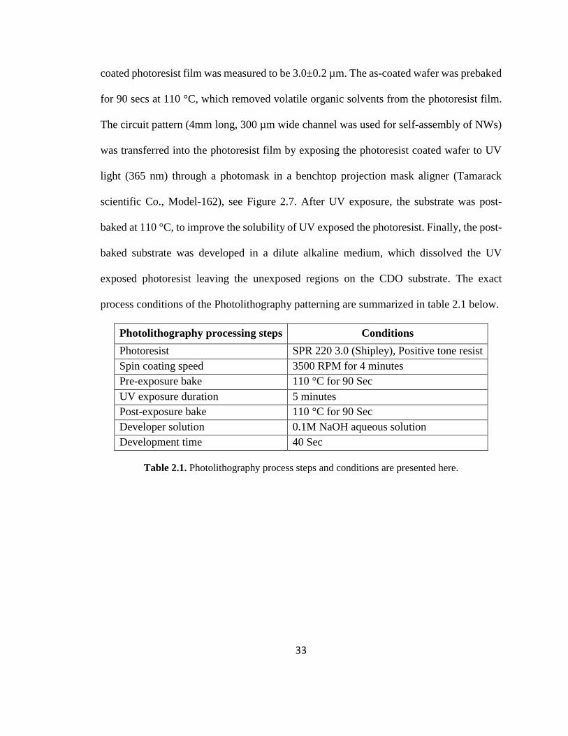
Photolithography processing steps Conditions
Photoresist SPR 220 3.0 (Shipley), Positive tone resist
Spin coating speed 3500 RPM for 4 minutes
Pre-exposure bake 110 °C for 90 Sec
UV exposure duration 5 minutes
Post-exposure bake 110 °C for 90 Sec
Developer solution 0.1M NaOH aqueous solution
Development time 40 Sec
Table 2.1. Photolithography process steps and conditions are presented here.

34
Figure 2.7. Digital photograph showing projection mask UV aligner (Tamarack scientific Co.,
Model-162) used for photolithography patterning (capable of patterning resolvable feature size of
1 µm).
2.2.8. Electrical characterization of self-assembled interconnect channels
The self-assembly of nanowires into photolithography patterned channel protocol is
discussed in detail in Chapter-5. Electrical characterization of the as assembled NWs
channel is carried out by fabricating the silver contact pads (High purity silver paint, SPI
supplies, CAS # 05002-AB, lot no # 1160331) on both ends of the channel and measured
the resistance values using Keithley programmable multimeter (Model-617).
35
CHAPTER THREE
COPPER NANOWIRES SYNTHESIS AND MAGNETIC FIELD ASSISTED
ALIGNMENT
In recent years, the synthesis of one dimensional (1D) nanostructures such as metallic NWs
(Ag NWs, Cu NWs, Au NWs, and Pt NWs) or carbon nanotubes (CNT) and their assembly
into functional devices have received special interest owing to its size and structure-
dependent unique properties. Among all metallic nanowires, copper nanowires (Cu NWs)
have attracted considerable attention lately due to their excellent electrical conductivity
(only 7% less conductive than silver), thermal, mechanical properties, and cheap precursor
cost (100 times cheaper than silver). In literature, various Cu NWs synthesis methods were
discussed such as chemical vapor deposition (CVD) 53, porous templates 26, 54,
hydrothermal/solvothermal57, and solution-based approaches33, 35, 58. However, in all the
above methods, the ability to precisely control the morphology and dimensions of NWs
was not possible. This thesis work adopted a solution based synthesis approach developed
by Zeng et al.,58 and Wiley et al.,33, 66. This thesis studied the effects of reagent
concentrations and synthesis temperature on morphology and aspect ratio controlled Cu
NWs synthesis.
The bottom-up or hybrid approaches of NWs assembly into nanodevices requires
simple, scalable and robust techniques to precisely control the orientation and positioning
of NWs. For Cu NWs, very limited success has been achieved in controlling the orientation
via electrochemical deposition of copper into a porous template26, 54, the thermal assisted
growth of freestanding NWs on a copper substrate67 and vertically aligned NWs in a CVD

36
technique53. The challenges in these techniques include high process complexity, poor
yield, and the as-grown NWs stuck to the substrate (hard to manipulate the location); so
Cu NWs are very challenging to transfer onto another desired substrate. To date, a simple
and robust technique to control the orientation of Cu NWs has not been demonstrated.
Here, for the first time, present work illustrates the magnetic field assisted unidirectional
alignment of Cu NWs by coating them with a thin layer (~20 nm) of ferromagnetic nickel
(Ni). Upon applying of the magnetic field, Cu/Ni NWs in the solution phase align in the
applied magnetic field direction and as the solvent dries aligned NWs deposit on the
substrate. In the subsequent sections, copper nanowires synthesis, an electroless coating of
nickel onto Cu NWs surface (Cu/Ni NWs) and magnetic field assisted alignment of Cu/Ni
NWs have been discussed in detail.
3.1. Copper nanowires synthesis
Copper nanowires were synthesized in a solution based approach, using copper nitrate
(Cu(NO3)2 2.5H2O) as a precursor, ethylenediamine (EDA, C2H4(NH2)2) as a growth
directing agent and hydrazine (NH2-NH2) as a reducing agent. The synthesis approach
followed the method published in the literature33, 58, 68, 69.
3.1.1. Cu NWs synthesis procedure: In brief, the procedure involved the mixing of a
copper nitrate solution (0.1M in DI water, 2 mL) to a freshly prepared aqueous NaOH (15
M, 40 mL) solution. Ethylenediamine (0.1 M, 266 µL) and hydrazine (9.66×10⁻³ M (35 µL)
to 4.09×10⁻³ M (15 µL)) reagents were added followed by a thorough mixing for 3 and 2
min respectively, after adding each reagent. Upon addition of hydrazine, the solution turned
clear suggesting the reduction of Cu+2 ions into Cu+1, After 30 minutes, a reddish-brown

37
cake formed at the air-water interface leaving the clear solution at the bottom, see Figure
3.1c. NWs were collected and washed several times with DI water and ethanol in a
centrifugation process, and finally stored in absolute ethanol solvent in a sealed glass vial.
Figure 3.1. Digital images of Cu NWs reaction solution before adding hydrazine (a) and after
adding hydrazine (b). After incubation for 30 minutes in hot water bath reddish-brown Cu NWs
cake floating at the air-water interface.
The chemical reactions involved in Cu NWs synthesis are shown below33, 35, 58. Cupric
(Cu2+) ions react with hydroxyl (OH-) ions and form cupric hydroxide complex ions (see
eq-1). The reducing agent, hydrazine, supplies electrons that are required for the reduction
of cupric ions to copper (Cu(0)). In the first step of the reduction process, cupric hydroxide
(Cu2+) complex ions are reduced to cuprous (Cu+) hydroxyl complex ions, (see eq-3)
(solution color turns from blue to clear, See Figure 3.1 a, b). And, in the second step, as
cuprous ion complexes (Cu+) are reduced to metallic copper (Cu0), (see eq-4). The capping
agent ethylenediamine (EDA), directs the copper atoms into unidirectional growth to form
nanowire morphology.

38
Cu2+ + 4OH- → Cu(OH)42- (blue solution) (1)
N2H4 + 4OH- → N2(g) + 4H2O + 4e- (2)
2Cu(OH)42- + 2e- → 2Cu(OH)2
- (clear solution) (3)
2Cu(OH)2- + 2e- → 2Cu(0) + 2OH- (4)
The amine functional groups in EDA capping agent act as a ligand to form the
coordinate covalent bond and interact with unsaturated surface atoms in the nanocrystals70.
The binding affinities of EDA are determined by the distinct atom geometries in various
crystal planes. The capping agents on the nanocrystal act as a physical barrier to restrict
the access of reagents in the capped facets and allowing the active growth process to occur
in the uncapped regions70.
Copper nanowire growth mechanism: The growth mechanism of copper nanowire in an
EDA and hydrazine assisted method have been discussed in detail by Wiley et al.,35, 71 In
brief, the mechanism involves during the initial stages of reduction process Cu(OH)42- ions
are reduced to Cu(OH)2- ions and Cu2O nanoparticles (the resultant solution appears as
translucent, see Figure 3.1b). The capping agent EDA helps in preventing the precipitation
of these Cu2O nanoparticles by capping the surface. And, keeping these nanoparticles
suspended in the solution are very crucial for the initiation of nanowire growth process.
The EDA coated Cu2O nanoparticles are further reduced by hydrazine to form irregular
shaped polycrystalline metallic copper aggregates with the size ranging from 200 to 500
nm in diameter70. The surface of these copper aggregates consists some of the pentagonal
twinned secondary particles (~40 nm) which will serve as a seed to sprout nanowire71. And,
39
during the nanowire growth process, EDA preferentially caps the higher surface energy
{100} crystal facets and leaving the lower energy {111} crystal facets (nanowire tip). The
Cu(OH)2- ions are reduced to metallic copper (Cu(0)) by hydrazine at nanowire tip which
possesses {111} crystal facet and promotes the anisotropic growth of nanowire
morphology35.
In this synthesis, NWs dimensions such as aspect ratio (length/diameter) and
surface morphology depended critically on the reagent concentrations and synthesis
conditions. Here, systematic studies of the effect of synthesis temperature and
concentration of reducing agent on NWs dimensions and morphology were investigated.
3.1.2. Effect of synthesis temperature
The effect of synthesis temperature was studied at 60, 70, 80 and 90 ̊ C respectively.
Except for the temperature, all other reaction parameters were kept constant. Figure 3.2
shows SEM images of Cu NWs synthesized at various temperatures, which indicates the
decrease in aspect ratio as the synthesis temperature increase. Image-J software analyzed
aspect ratios of Cu NWs synthesized at various temperatures are shown in Table 3.1. As
the synthesis temperature increased to more than 90 °C, all the copper atoms agglomerated
and formed micrometer-sized (200 nm to 3 µm) sized copper aggregates. It was suggested
that the formation Cu-NWs is controlled by EDA which caps the side-wall surface of NWs.
The potential reason for the formation of micron size aggregates at a higher temperature
could be due to desorption of EDA from the NW surface, coupled with lower super-
saturation of Cu atoms at temperatures above 90 °C.

40
Figure 3.2. SEM images of copper nanowires synthesized at 60 °C (a), 70 °C (b), 80 °C (c), and
90 °C (d) respectively.
Temp.
(°C) Average
Length
(µm)
Average Diameter
(nm)
Aspect ratio
60 32 ± 7 160 ± 30 200
70 25 ± 6 170 ±50 147
75 15 ± 4 210 ± 60 71
80 7 ± 2 220 ± 30 32
Table 3.1. Average lengths, diameters and aspect ratios of copper nanowires synthesized at 60, 70,
80, and 90 °C respectively.

41
3.1.3. Effect of reducing agent concentration
Nanowire anisotropic growth and thickening mechanisms were discussed by Wiley et al.,
and highlight the importance of reducing agent (hydrazine) concentration33, 35, 68. Similarly,
the present investigation focused on the effect of hydrazine concentration on surface
morphology and the aspect ratio of Cu NWs.
Figure 3.3. SEM images of Cu NWs synthesized using high concentration (35 µL) of reducing
agent, Images shown at low a) and high b) magnification scales. TKD overlaid SEM image shown
in c), and out-of-the-page (Z) direction crystallographic orientation is shown in d), highlight the
thick and highly particle decorated NWs. e) crystal plane to color mapping scale.

42
In these studies, except for hydrazine, all other reagent concentrations and
conditions were maintained constant. See experimental section (3.1.1.) for more
information about the synthesis procedure. Figure 3.3a & b shows SEM images of Cu NWs
synthesized using a high concentration (9.66×10⁻³ M, 35 µL) of reducing agent hydrazine.
These images revealed that as-synthesized NWs featured low aspect ratio (L/D ~20) with
rough surface morphology suggestive of Cu nanoparticle decoration on the NW surface.
To characterize the nanoparticle decoration, this study examined the crystallographic
orientational mapping of these particulates on the NW surface using SEM. Transmitted
electron backscattered diffraction (t-EBSD) orientational mapping images shown in Figure
3.3 c & d displayed various crystallographic orientations of these (adsorbed) nanoparticles.
Figure 3.4. SEM images of copper nanowires synthesized using an intermediate concentration of
hydrazine (8.28x10⁻³M, 30 µL).
At an intermediate concentration of hydrazine (8.28x10⁻³ M, 30 µL), the synthesis
yielded nanowires surface decorated with comparatively small particles or spikes; See

43
Figure 3.4. As the hydrazine concentration was further reduced to 5.73x10⁻³ M (21 µL), the
resulting NW exhibited high aspect ratio (~250) and a particle-free and comparatively
smooth surface, see SEM images in Figure 3.5a & b. The average length and the diameter
of NWs was ~30±4 µm and 120 ± 20 nm, respectively. The t-EBSD pattern of the same
batch of NWs, shown in Figure 3.5c & d, suggested a comparatively smooth and single
crystalline surface. The dark regions in the orientational mapping images represented poor
electron transmission.

44
Figure 3.5. SEM images of Cu NWs synthesized using a low concentration of reducing agent
shown at low a) and high b) magnification scales. TKD c), and out-of-the-page (Z) direction
crystallographic orientation in d), showing particle free thin Cu NWs. And, e) showing a color map
for crystallographic planes. Histograms in f) and g) represents the length and diameter distributions
of as-synthesized Cu NWs extracted from samples containing >200 NWs.
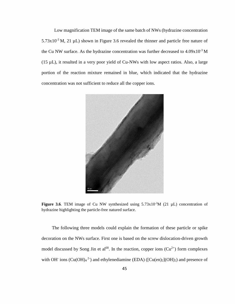
45
Low magnification TEM image of the same batch of NWs (hydrazine concentration
5.73x10⁻³ M, 21 µL) shown in Figure 3.6 revealed the thinner and particle free nature of
the Cu NW surface. As the hydrazine concentration was further decreased to 4.09x10⁻³ M
(15 µL), it resulted in a very poor yield of Cu-NWs with low aspect ratios. Also, a large
portion of the reaction mixture remained in blue, which indicated that the hydrazine
concentration was not sufficient to reduce all the copper ions.
Figure 3.6. TEM image of Cu NW synthesized using 5.73x10⁻³M (21 µL) concentration of
hydrazine highlighting the particle-free natured surface.
The following three models could explain the formation of these particle or spike
decoration on the NWs surface. First one is based on the screw dislocation-driven growth
model discussed by Song Jin et al68. In the reaction, copper ions (Cu2+) form complexes
with OH- ions (Cu(OH)4 2-) and ethylenediamine (EDA) ([Cu(en)2](OH)2) and presence of

46
these complex ions cause a decrease in the supersaturation of nanowire anisotropic growth.
When an excess of the reducing agent results in a reduction of these copper complex ions
into copper atoms all at once, a decrease in these complex ion concentrations causes an
increase in the supersaturation at the tip of the nanowires68. Hence, NWs stop growing in
the axial direction and promotes the growth of nanowire in the lateral axis and may form
particles with various crystal planes which are grown at the screw dislocation sites on the
nanowire surface. Whereas at moderate hydrazine concentration, the presence of copper
complex ions decreases the supersaturation and hence causes the growth of NWs in
longitudinal axis leading to high aspect ratio NWs.
The second hypothesis is based on the EDA as a facet selective promoter of NW
growth mechanism which is discussed by Wiley et,al69. Presence of excess hydrazine keeps
the NW surface free of Cu oxide and promotes deposition of copper on the NW surface
which results in thicker NWs. Whereas at a moderate concentration of hydrazine, the NW
surface remains oxidized due to the presence of high OH- ions and prevents the growth in
NW lateral axis direction and promotes the longitudinal axis ((100) facet) growth which
ultimately results in high aspect ratio NWs.
The third hypothesis is an excess of reducing agent concentration results in a
reduction of copper ion complexes to copper atoms all at once, and these highly
concentrated copper atoms agglomerate to form multiply twinned nanoparticles. TEM
images shown in Figure 3.7 a & b shows the presence of nanoparticles in the solution along
with NWs, and perhaps during the nanowire growth, some of the particles may stick onto
the nanowire surface leading to NW thickening. See Figure 3.7c. The mechanism reported

47
by Wiley et, al. supports this hypotheses 33. The exact reason behind the particle decoration
is not completely understood for now. Nevertheless, experimental studies show how the
concentration of reducing agent affects the morphology and allows the determination of
the optimized concentration to synthesize high aspect ratio and particle free nanowires.
Figure 3.7. Low magnification bright field a), and high magnification dark field b), TEM image
showing the presence of nanoparticles. Bright field image c), showing nanoparticles sticking to the
surface of the nanowire at multiple sites (pointed out with arrows).
3.2. Electroless plating of nickel (Ni) on Cu NWs surface
3.2.1. Nickel electroless plating procedure: Electroless plating of nickel onto the Cu NWs
surface was conducted by a slightly modified version of the method discussed by Wiley et
al.59, 72. In brief, the procedure involved mixing of Ni(NO3)2 (0.1 M in DI water, 0.4 mL)
and hydrazine (0.16 M (600 µL)) reagents with a 10 mg of Cu NWs (dry mass) suspension
in ethylene glycol (20 mL). The above solution was thoroughly vortex mixed for 5 minutes
and heated in an oil bath at 120 °C. After heating for 10 minutes, the solution turned clear
and dark-colored nickel coated Cu NWs (Cu/Ni NWs) floated at the air-water interface due
to trapped N2 gas bubbles generated in the reaction, See Figure 3.8.

48
Figure 3.8. Digital photographs are showing nickel electroless plating mother solution (a mixture
of Cu NWs / Ni(NO3)2 / Hydrazine in ethylene glycol solvent) a). After heating at 120 °C for 10
minutes, floating of dark-colored nickel coated Cu NWs at the air-water interface can be observed
in b), and magnetic response of Cu/Ni NWs towards neodymium disc magnets is shown in c).
When a disc magnet was placed next to the freshly prepared Cu/Ni NWs solution, it
attracted the mass of dark cupronickel nanowires, see Figure 3.8c. The nickel coating
thickness on Cu NWs surface was studied by using EDS elemental mapping, See Figure
3.9, which revealed nickel layer on the CuNW surface of ~20 nm thickness. Also, the
presence of oxygen at the interface of Cu and Ni indicated oxidized copper NW surface.
But the nickel surface did not show significant oxidation implying metallic surface.
Electroless coating of nickel would be advantageous in a few aspects, such as
protecting the core copper from further oxidation and for reducing the contact resistance
between nanowires due to strong binding resulting from the ferromagnetic interaction.
Furthermore, the ferromagnetic nature of the nickel allowed a directional control over the
orientation of the NW by applying an external magnetic field.

49
Figure 3.9. SEM image of nickel coated copper nanowire (Cu/Ni NW) shown in a), and elemental
mapping image showing the distribution of copper core and nickel coating on the surface b). In
between the copper and nickel layers copper oxide (green color) can be observed.
3.3. Magnetic field assisted alignment
Figure 3.10. Digital photographs of electromagnet setup (GMW, Model-3470) used for controlling
the orientation of Cu/Ni NWs are shown in a) and b). Digital photograph of well-aligned NWs in
solution at 2500 G of applied magnetic field and after turning off the magnetic field to H = 0G, no
rearrangement of NWs chains can be observed in d).

50
Controlling the orientation of nanowires is very critical for the assembly of NWs
into complex nano or microelectronic devices. Here the magnetic field assisted alignment
was explored to systematically control the orientation of Cu/Ni NWs on a centimeter scale
area. The GMW electromagnet system provided the uniform magnetic field in between its
poles (see Figure 3.10). The alignment procedure involved deposition of the Cu/Ni NWs
aqueous solution on a given substrate as shown in Figure 3.10 to align NWs aligns in the
applied magnetic field direction. Each NW effectively acted like a nanobar magnet in the
field and formed NWs chains by connecting with each other in a head to tail fashion. And,
surprisingly even after turning off the magnetic field (H = 0G) NWs chains remained in a
well-organized manner, see Figure 3.10 d. This suggests owing to the ferromagnetic, (not
paramagnetic) nature of nickel all the NWs remained magnetized. This led to a strong
binding to each other even after turning off the magnetic field. These types of well-aligned
nanowire arrays are very attractive for nanowire-based devices owing to its excellent
percolation network formation, uniformity and comparatively lower NW-NW junction
resistance45.
Figure 3.11 shows the optical microscopic images of Cu/Ni NWs alignment in the
presence and the absence of an applied magnetic field. When the NWs solution was
allowed to dry under ambient conditions in the absence of a magnetic field, typically all
the NWs arranged in random directions forming agglomerations due to Van der Waal
forces of attractions. However, when the external magnetic field was applied, all the NWs
acted like nanobar-magnets and aligned in the applied magnetic field direction, See Figure
3.11b. Furthermore, strings of NWs formed suggesting end-to-end attachment of NWs due
51
to favorable magnetic interaction (i.e., the attraction between north and south poles of the
neighboring NWs). Following two steps of deposition and alignment in orthogonal
directions produced an NW mesh or crossed arrays (Figure 3.11c) useful for fabricating
flexible and transparent electrode preparation45, 49.
Systematic studies of alignment phenomenon were undertaken. In the absence of a
magnetic field, all the NWs arranged in the random directions with an average angle of 45°
with respect to the hypothesized axis and the resulting deposits showed agglomerations.
Whereas, with an applied magnetic field (2500 G), the majority of the NWs aligned with
an angle less than 10° with respect to the applied magnetic field direction (see angular
distribution in Figure 3.11d). The NWs alignment angle distribution with respect to the
applied magnetic field direction (in case of a magnetic field applied) and hypothesized axis
(in case of no magnetic field applied) were determined by using Image-J application, see
Appendix-B for a detailed protocol. Also, the average angle with respect to the magnetic
field direction depended on the field strength. Therefore, the alignment distribution
function was determined as a function of the magnetic field strength that varied from 0 G
to 2500 G.

52
Figure 3.11. Optical microscope images of Cu/Ni NWs when they are allowed drying in the
absence (a), and in the presence of applied magnetic field (2500 Gauss) (b). Image (c) shows the
NWs mesh prepared by depositing a 2nd layer of NWs orthogonally. The histogram in (c) highlights
the NWs orientation distribution with respect to the applied magnetic field direction.
3.3.1. Effect of magnetic field strength on NWs alignment order
As discussed in the previous sections, each nickel coated Cu NW (Cu/Ni NW) acted like a
nano bar-magnet and responded to the externally applied magnetic field. Alignment
strength of these bar magnets was explored by depositing 100 µL of Cu/Ni NWs solution
(0.5 mg/mL) on the 1x1cm sized wafer substrate and the solvent was allowed to evaporate
in the presence of a magnetic field with strength varying from 0 to 2500 G. See Figure
3.12. When there was no magnetic field (0 G), all the NWs aligned in the random directions

53
and formed agglomerations. As the magnetic field strength increased, Cu/Ni NWs began
to form chains by connecting the NWs in an end-to-end fashion. As the field strength
increased, NWs chain lengths tended to increase.
Figure 3.12. Optical micrographs showing alignment order of Cu/Ni NWs at various applied
magnetic field strength from 0 G to 2500 G.
Excellent alignment with an average alignment angle of ~12° was achieved at
1500G. As the field strength is further increased to the 2500G, the average alignment angle
decreased to ~8°. The observation suggested that at least a 1500 G magnetic field strength
is required to get a reasonably good alignment. The average alignment angle tended to be
further reduced and reached saturation at higher field strengths, See Figure 3.13. The
distribution function for the corresponding NWs is shown below along with a summary of
parameters in the in the accompanying table.

54
Figure 3.13. Plot showing average NWs alignment angle with respective to the applied magnetic
field direction, at various field strength from 0 G to 2500 G. The inset image describes the
alignment angle definition.
Figure 3.14. Gaussian peak fitting plots are showing NWs alignment distribution with respect to
the applied magnetic field strength from 0 to 2500 Gauss.
Orientation distribution histograms of Cu/Ni NWs measured as a function of
magnetic field strengths were fitted to a Gaussian equation below.
55
BAeN
2)(
)(
A and B are a normalization constant and a constant background fitting parameter. N(θ) is
a number of nanowires oriented at angle θ in a bin size of 0.2 radians. <θ> and Δθ are the
average absolute value of the NW orientational angle and the width of the distribution
respectively. The best-fit parameters and respective curve fitting uncertainties appear in
Table 3.2.
Table 3.2: List of field dependent parameters.
3.4. Summary of copper nanowires synthesis and magnetic field assisted alignment
Control over nanowire surface roughness, aspect ratio, and alignment are very important
for their device application. In this thesis research, a solution based synthesis method was
optimized with respect to the reducing agent concentration to synthesize the high aspect
ratio NWs with a smooth surface. Also, the effect of synthesis temperature on the aspect
ratio of nanowires was investigated. As the synthesis temperature increased, the aspect
ratio of NWs decreased. In the case of controlling the alignment of Cu NWs, the previous
researcher had reported very limited success via CVD, electrochemical deposition in a
porous template and thermal assisted growth of vertically aligned NWs. For the first-time
simple magnetic field based alignment of NWs on macroscopic wafer-scale was realized
Field
Strength(gauss)
θ(radian) Δθ (radian)
000 0.7±0.1 0.4±0.2
500 0.75±0.05 0.25±0.08
1000 0.54±0.03 0.21±0.03
1500 0.23±0.07 0.41±0.08
2000 0.13±0.09 0.37±0.09
2500 0.3±0.7 0.5±0.3

56
by coating Cu NWs with a thin layer of ferromagnetic nickel. The nickel coating would be
further advantageous in protecting the copper core from oxidation.

57
CHAPTER FOUR
SURFACE DERIVATIZATION OF CARBON DOPED SILICON DIOXIDE
(CDO) WAFER
Carbon doped silicon dioxide (CDO), a highly nanoporous low-k dielectric, was
chosen as a substrate for the fabrication of nanowires based interconnects. The self-
assembly of NWs into interconnect structures on CDO wafer required surface preparation
of CDO to attract and strongly hold the nanowires after deposition. In this work, thiol (-
SH) functionalization of the CDO surface and strong interaction of thiol to copper and
nickel was explored. Thiol functionalization of the CDO surface was achieved via a novel
approach developed to selectively functionalize the surface exposed silicon hydroxide (Si-
OH) functional groups60. The hydrophilic Si-OH functional groups are generated during
various steps in chip integration processing and cause undesirable moisture uptake which
adversely increases the dielectric constant (k) of CDO. We addressed this issue by
selectively derivatizing the surface exposed hydrophilic Si-OH functional groups to highly
hydrophobic long alkyl chain (Si-R, R = octadecyl chain). The dense layer of octadecyl
chains then acts as a moisture repellent thin film. This chapter provides the details of CDO
film derivatization by octadecyl and thiol chains along with CDO surface characterization
by XPS, IR, capacitance-voltage and contact angle techniques.
4.1. Introduction
Some of the biggest achievements in the past half-century involved the development
of the microprocessor industry. To address a large number of transistors integrated into
microprocessors, a sophisticated multilayer wiring, the so-called, interconnect architecture,
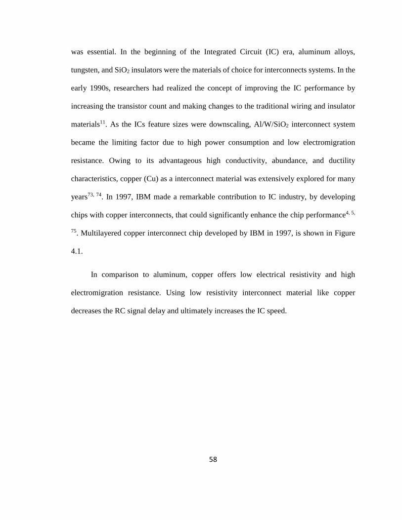
58
was essential. In the beginning of the Integrated Circuit (IC) era, aluminum alloys,
tungsten, and SiO2 insulators were the materials of choice for interconnects systems. In the
early 1990s, researchers had realized the concept of improving the IC performance by
increasing the transistor count and making changes to the traditional wiring and insulator
materials11. As the ICs feature sizes were downscaling, Al/W/SiO2 interconnect system
became the limiting factor due to high power consumption and low electromigration
resistance. Owing to its advantageous high conductivity, abundance, and ductility
characteristics, copper (Cu) as a interconnect material was extensively explored for many
years73, 74. In 1997, IBM made a remarkable contribution to IC industry, by developing
chips with copper interconnects, that could significantly enhance the chip performance4, 5,
75. Multilayered copper interconnect chip developed by IBM in 1997, is shown in Figure
4.1.
In comparison to aluminum, copper offers low electrical resistivity and high
electromigration resistance. Using low resistivity interconnect material like copper
decreases the RC signal delay and ultimately increases the IC speed.

59
Figure 4.1. Image of the multilayered integrated circuit (IC) using Cu/W/ SiO2 dielectric materials,
developed by IBM in 19974.
As the transistor count and interconnect density increase, the RC signal delay, and
power dissipation also increase because of increased capacitive coupling between densely
packed metal lines. Since the RC signal delay and power consumption all are directly
related to dielectric constant (k) of the inter-metal dielectric material, many efforts have
been devoted to replacing the standard silicon dioxide (k = 3.9 to 4.2) with an ultra-low k
material76. The Dielectric constant (k) is defined as the ratio between permittivity of a
substance to the permittivity of vacuum as shown in the below equation. In Table, 4.1 k
values of common materials are shown.
Dielectric constant (𝑘) = Permitivity of substance
Permitivity of vacuum
Due to low k value, many organic compounds are considered as a good low k
dielectric material, but organics have limitations associated with poor thermal and
mechanical stability. Furthermore, inorganic materials show good mechanical and thermal

60
stabilities, but they possess higher k and more serious moisture sensitivity, requiring an
additional liner and capping layers77, 78. Hybrid films, with organic and inorganic materials,
have been a promising approach for low-k materials with stable properties. Among hybrid
type materials, carbon doped silicon oxide (CDO) material has attracted more attention
owing to its low-k, and compatible mechanical and thermal properties3, 79-82. Hence, in
modern ultra-large-scale integrated circuit (ULSI) devices CDO has been a choice as a
low-k insulator.
Substance k - value
Vacuum 1
Polyethylene 2.25
Carbon Doped Silicon Oxide (CDO) 2.2 to 3.0
SiO2 3.9
Silicon 11.68
Water ~ 80
Table 4.1. Dielectric constant (k) values of various substances.
4.2. CDO as a low-k material
Over the last few years, the classic SiO2 insulator used to separate metallic
interconnect lines are being replaced by materials of lower k. Lower k improves signal
propagation delay. The lower the k value shorter the propagation delay. Strategies to
realize lower k materials include (1) Introduction of carbon in SiOx network structure, by
using so-called CDO materials (reviewed in this work). CDO film preparation and
chemical structures etc. are discussed in detail in the following sections. (2) Incorporating
porosity (note: air has lowest k ~1). Porosity is inversely related to k-value; as the porosity

61
increases, k values decreases. In the as deposited CDO film, nanopores can be introduced
by plasma curing processes. The plasma burns off organic moieties and leaves nanopores
in the film.
4.3. Review on CDO film preparation and chemical structure
Carbon doped silicon oxide (CDO), composed of Si, C, O, and H (SiCOH), is
deposited on Si (100) surface by plasma enhanced chemical vapor deposition (PECVD)
from mixtures of silicon and an organic precursor80. In a PECVD reactor, the plasma is
sustained by 13.56 MHz rf power. The silicon and organic precursors are carried by He gas
into the plasma chamber. SiCOH film preparation employs various silicon precursors such
as tetramethylsilane80, hexamethyldisiloxane 81, tetramethyltetrasiloxane82. In the presence
of plasma, precursor molecules break down into fragments and deposit on the Si wafer.
The deposited films are annealed at 400 ̊ C. The annealing step removes thermally unstable
organic fragments and creates porosity in the material which enables the adjustment of the
k between 2.8 to 2.05. Post thermal treatment also causes extensive cross-linking of Si, C,
and O to form Si-Si, Si-O-Si, Si-CH2-Si and Si-CH2-O-Si moieties. The annealing process
depending on the duration and temperature causes the loss of –CHn- groups and results in
the formation of -Si-C- linkages and nanopores in the film83.
An alternative method to thermal annealing is plasma curing which can reduce k (k =
2.0 to 2.2). The plasma curing process creates nanopores and improves the crosslinking
which helps in improving the mechanical strength of the film84. The plasma curing process
is an industry preferred method, owing to its advantageous lower operating temperature,

62
uniformity, cost-effectiveness, shorter processing time, and produces improved mechanical
strength of the film.
4.4. Review on CDO damage and repairing methodologies
4.4.1. Review on CDO damage by plasma processing
Interconnects in modern ICs integrate multilayers of copper wiring and insulating
low k materials (See Figure 4.1). They are fabricated using a combination of optical
lithography and copper electroplating in a process known as the Dual Damascene (DD)
method37. In optical lithography, a photoresist film made up of organic polymers, and
photosensitive compounds serve as a patternable and sacrificial stencil. An optical image
of the desired circuit pattern of trenches and vias are projected on the photoresist film
coated on top of the CDO layer. Photochemical reactions in the light exposed regions alter
the solubility of the photoresist film regio-specifically. In the developer solution, the film
undergoes preferential dissolution (positive tone) or dissolution inhibition (negative tone)
to expose the underlying CDO transferring an image of the desired circuit pattern on the
chip.

63
Figure 4.2. a) Chemical structure of porous cage networked structure of as-prepared CDO film
from TMCTS precursor82, and b) chemical structure of plasma damaged film (R, represents an
extension of Si-O-Si backbone structure)85.
This pattern is etched into the exposed CDO through plasma etching which opens
up the electrical contacts in the lower layer. Subsequently, metallic copper is selectively
and electrochemically plated in the etched vias/trenches, while avoiding its deposition on
top of the undissolved electrically insulating photoresist film. After electroplating, the
remaining sacrificial photoresist film is subjected to oxygen plasma ashing to remove
organics as CO/CO2 and water as ultimate byproducts86. Furthermore, oxygen radicals
generated during the plasma processing react with the functional groups of the CDO film,
breaking Si-CH3, Si-H bonds, and creates dangling bonds of silicon. These dangling bonds
can easily react with hydroxyl ions in the plasma environment to form Si-OH bonds (see
Figure 4.2)) 85. The resulting increase in the number of hydrophilic Si-OH groups in the
CDO films makes the film more polar, hydrophilic and allows moisture uptake (water k =
~80). Absorbed moisture increases the k value (note the dielectric constant of water is 80!)

64
and leakage current (due to protonic conduction) thereby compromising the quality of the
CDO87.
4.4.2. Review on CDO repairing methodologies
Several approaches have been investigated to minimize the damage of porous CDO
ultra-low k film. One method involves protecting the CDO film from oxygen plasma
damage by depositing a thin inert SiNx passivation layer. The SiNx film is generated from
a thin layer of hybrid-organic-siloxane-polymer (HOSP) subjected to NH3 plasma
treatment88. This inert layer can enhance the resistance of the HOSP film to moisture uptake
and O2 plasma attack. Helium (He) plasma treatment as a post CDO deposition has also
been investigated to reduce the O2 plasma damage on the CDO films89. Treating the O2
plasma damaged CDO with a hydrogen (H2) plasma to repair the damage by reducing
silanol to silicon hydride has also been explored89. However, CDO repairs by He, NH3 and
H2 plasma treatments cause a loss of CDO film thickness (by reducing porosity) and
irreversibly modify the network of the SiCOH chemical structure. Etching of plasma
damaged low k CDO layer by dilute HF solution has been investigated, but the
concentration of HF solution and duration of treatments are very critical to prevent further
etching of the undamaged CDO layer90.
Another approach to preventing moisture uptake in the damaged CDO is to convert
surface silicon hydroxyl (Si-OH) functional groups to hydrophobic Si-O-Si(CH3)3 moieties
by treating with hexamethyldisilazane (HDMS)62. However, the resulting single carbon (-
CH3, Methyl) termination is too thin to prevent the further attack from oxygen and
moisture. Hence, it is necessary to find a way to selectively derivatize hydrophilic

65
functional groups (Si-OH) to hydrophobic, without disturbing the backbone structure of
the CDO film.
4.5. Results of developed pathway for selective derivatization of silanol
4.5.1. Developed scheme for surface derivatization
A gentle and spatially selective approach for the modification of surface exposed,
hydrophilic silicon hydroxyl (Si-OH) functional groups to hydrophobic hydrogen-
terminated (Si-H) is developed. The stability and surface hydrophobicity was further
enhanced by long alkyl chain derivatization of the silicon hydride (Si-R, R= C18H37) as
shown in Scheme 4.3. Compared to methyl groups, long chain alkyl groups form a thicker
and more compact hydrophobic film that blocks moisture uptake effectively91. The
significant advantage of this approach is that the selective derivatization occurs only on the
exposed or surface silicon hydroxyl (Si-OH) groups of CDO film without damaging the
rest of the nano-porous cage structure. Additionally, silicon hydride formed during the
intermediate stage may be further derivatized with different reactants to provide new
surface functionalities92. For example, it provides a convenient route for the insertion of
additional functional groups such as terminal thiol (-SH) or amine (-NH2) alkene structure.
Scheme 4.1. Schematic of the new reaction pathway for hydrogen termination and octadecane (Si-
R, R= C18H37) derivatization.

66
The viability of this approach has been established methodically by preliminary
studies of derivatization of silanol groups in organic molecules, silica gel, SiOx wafer and
CDO as shown in Figure 4.2 below.
Scheme 4.2. Schematics of various compounds considered for testing surface derivatization
reaction, a) tert-Butyldimethylsilanol b) silica gel, and c) SiOx wafer and d) nano porous carbon
doped silicon oxide (CDO) wafer.
Common synthetic procedure: The first step in the reaction scheme employed 0.1 M
triflic anhydride ((CF3SO2)2O) in anhydrous toluene at 50-60 ˚C for 48 hours to esterify
the Si-OH functional group to yield silyltrifluoromethane sulfonate (Si-O-Tf, where Tf
indicates the SO2CF3 group). In the second step, 0.1 M DIBAL-H (di-isobutylaluminum
hydride, (CH3)2CHCH2)2AlH) reagent at 50-60 ˚C for 48 hours reduced the triflate
intermediate (Si-O-(SO2)CF3) to silicon hydride. Because hydrogen-terminated silicon is
unstable, Si-H was further treated with 1-octadecene (CH3(CH2)15CH=CH2) in the
presence of UV light (254 nm) for 2 hours to produce Si-R (Si-C18H37). All reactions were
carried out in dry N2 within a glovebox. Between each set of reactions, silica gel, SiOx
wafer, and CDO wafers were thoroughly washed with anhydrous toluene.
4.5.2. Results on organic molecules

67
Scheme 4.3. Schemes of a) Synthesis of TBDMS Triflate and tert-Butyldimethylsilane, b)
Synthesis of tert-Butyltrimethylsilane c) Synthesis of Triphenylsilane.
a) tert-Butyldimethylsilanol
tert-Butyldimethylsilanol ((CH3)3CSi(CH3)2OH) was used as a control molecule
for the reaction scheme shown in Figure 4.3a. Reaction kinetics were studied by 1H-NMR
spectroscopy and reaction products were confirmed by 19F-NMR, FTIR and Gas
Chromatography-Mass Spectrometry (GC-MS). Transformation of the molecule to triflate
and hydride molecules can be readily tracked by NMR, IR, and GC-MS techniques
enabling optimization of the reaction conditions and yield. The kinetics of the triflation
reaction was monitored by 1H-NMR of the reaction mixture over 72 hours, within 48 hours
the reaction goes to completion (see Figure 4.3). The product of the reaction was further
confirmed by parent ion peak at 265.0 g.mol-1 in the mass spectrum.
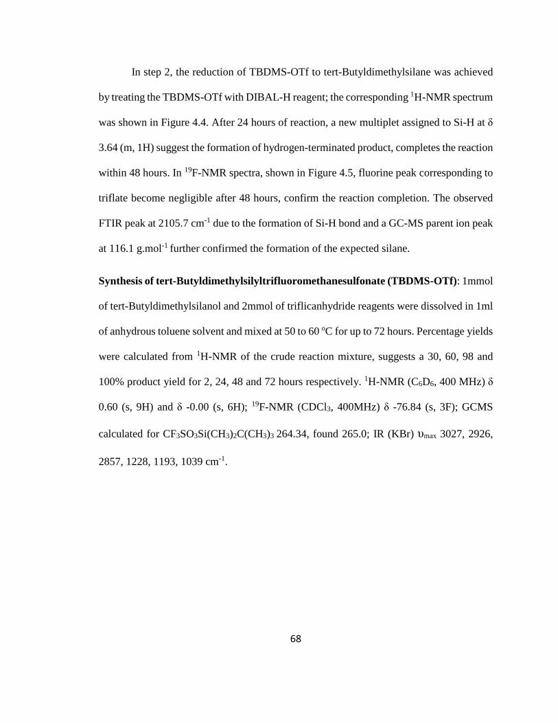
68
In step 2, the reduction of TBDMS-OTf to tert-Butyldimethylsilane was achieved
by treating the TBDMS-OTf with DIBAL-H reagent; the corresponding 1H-NMR spectrum
was shown in Figure 4.4. After 24 hours of reaction, a new multiplet assigned to Si-H at δ
3.64 (m, 1H) suggest the formation of hydrogen-terminated product, completes the reaction
within 48 hours. In 19F-NMR spectra, shown in Figure 4.5, fluorine peak corresponding to
triflate become negligible after 48 hours, confirm the reaction completion. The observed
FTIR peak at 2105.7 cm-1 due to the formation of Si-H bond and a GC-MS parent ion peak
at 116.1 g.mol-1 further confirmed the formation of the expected silane.
Synthesis of tert-Butyldimethylsilyltrifluoromethanesulfonate (TBDMS-OTf): 1mmol
of tert-Butyldimethylsilanol and 2mmol of triflicanhydride reagents were dissolved in 1ml
of anhydrous toluene solvent and mixed at 50 to 60 oC for up to 72 hours. Percentage yields
were calculated from 1H-NMR of the crude reaction mixture, suggests a 30, 60, 98 and
100% product yield for 2, 24, 48 and 72 hours respectively. 1H-NMR (C6D6, 400 MHz) δ
0.60 (s, 9H) and δ -0.00 (s, 6H); 19F-NMR (CDCl3, 400MHz) δ -76.84 (s, 3F); GCMS
calculated for CF3SO3Si(CH3)2C(CH3)3 264.34, found 265.0; IR (KBr) υmax 3027, 2926,
2857, 1228, 1193, 1039 cm-1.

69
Figure 4.3. 1H-NMR (C6D6, 400 MHz) reaction progress study of TBDMS Triflate synthesis at 2,
24, 48 and 72 hours respectively. Increase in peak intensities at δ 0.60 (s, 9H) and δ -0.00 (s, 6H)
corresponding to TBDMS Triflate can be observed.
Synthesis of tert-Butyldimethylsilane: 1mmol of tert-Butyldimethylsilyltrifluromethane
sulfonate and 2 mmol of DIBAL-H reagents were dissolved in 1ml of anhydrous toluene
solvent and mixed at 50 to 60 oC for up to 72 hours. Percent yields were calculated from
1H-NMR of the crude reaction mixture, suggests 0, 61, 89 and 91% product conversion
after 2, 24, 48 and 72 hours respectively. 1H-NMR (CDCl3, 400 MHz) δ 3.64 (m, 1H), δ
0.88 (s, 9H), δ 0.02 (d, J = 3.1 Hz, 6H); GCMS calculated for HSi(CH3)2C(CH3)3 116.28,
found 116.10; IR (KBr) υmax 3027, 2926, 2857, 2105 cm-1.

70
Figure 4.4. 1H-NMR (CDCl3, 400 MHz) reaction progress study of tert-Butyldimethylsilane
synthesis at 2, 24, 48 and 72 hours respectively. Peaks in the regions of δ 0.00 and δ 3.64 ppm were
magnified and shown on the right and left-hand side of the original spectra. The appearance of
multiplet at 3.64 (m, 1H) after 24 hours of reaction suggests the formation of the hydrogen-
terminated product. The decrease in the peak intensities of reactant and increase in peak intensities
of the product can be observed here.
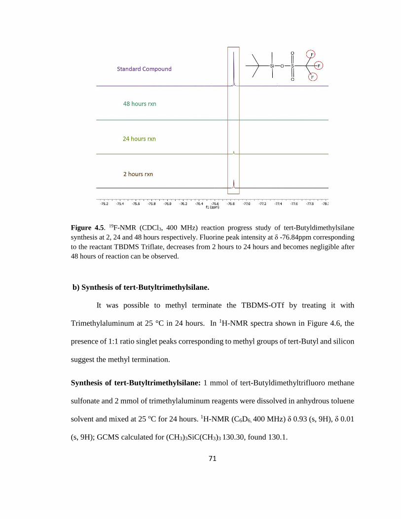
71
Figure 4.5. 19F-NMR (CDCl3, 400 MHz) reaction progress study of tert-Butyldimethylsilane
synthesis at 2, 24 and 48 hours respectively. Fluorine peak intensity at δ -76.84ppm corresponding
to the reactant TBDMS Triflate, decreases from 2 hours to 24 hours and becomes negligible after
48 hours of reaction can be observed.
b) Synthesis of tert-Butyltrimethylsilane.
It was possible to methyl terminate the TBDMS-OTf by treating it with
Trimethylaluminum at 25 °C in 24 hours. In 1H-NMR spectra shown in Figure 4.6, the
presence of 1:1 ratio singlet peaks corresponding to methyl groups of tert-Butyl and silicon
suggest the methyl termination.
Synthesis of tert-Butyltrimethylsilane: 1 mmol of tert-Butyldimethyltrifluoro methane
sulfonate and 2 mmol of trimethylaluminum reagents were dissolved in anhydrous toluene
solvent and mixed at 25 oC for 24 hours. 1H-NMR (C6D6, 400 MHz) δ 0.93 (s, 9H), δ 0.01
(s, 9H); GCMS calculated for (CH3)3SiC(CH3)3 130.30, found 130.1.

72
Figure 4.6. 1H-NMR (DMSO-d6) reaction progress study of tert-Butyltrimethylsilane synthesis at
2, 24 hours of reaction. A gradual increase in peak intensities at δ 0.93 (s, 9H), δ 0.01 (s, 9H) with
1:1 ratio corresponding to methyl groups of the product i.e., tert-butyl and 3 methyl groups on
silicon can be observed.
Thus, DIBAL-H and Trimethylaluminum reagents successfully converted the
triflate ester of silanol to hydride and methyl groups. In addition to tert-
Butyldimethylsilanol, the hydrogen termination on Ethoxytriphenylsilanol was confirmed.
c) Ethoxytriphenylsilane
In addition to tert-Butyldimethylsilanol, the reaction pathway on
Ethoxytriphenylsilane was tested as shown in Scheme 4.3c. 1H-NMR data of the expected
silane suggest the hydrogen termination of silicon by DIBAL-H reduction (see Figure 4.7).
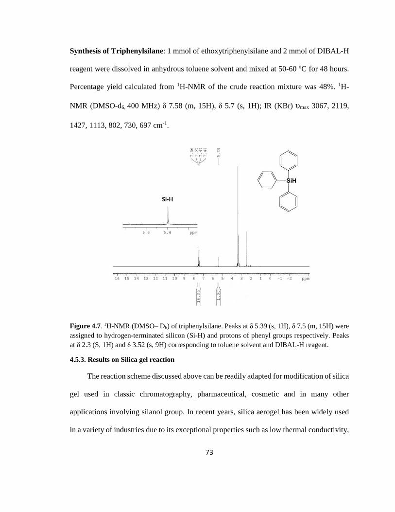
73
Synthesis of Triphenylsilane: 1 mmol of ethoxytriphenylsilane and 2 mmol of DIBAL-H
reagent were dissolved in anhydrous toluene solvent and mixed at 50-60 oC for 48 hours.
Percentage yield calculated from 1H-NMR of the crude reaction mixture was 48%. 1H-
NMR (DMSO-d6, 400 MHz) δ 7.58 (m, 15H), δ 5.7 (s, 1H); IR (KBr) υmax 3067, 2119,
1427, 1113, 802, 730, 697 cm-1.
Figure 4.7. 1H-NMR (DMSO– D6) of triphenylsilane. Peaks at δ 5.39 (s, 1H), δ 7.5 (m, 15H) were
assigned to hydrogen-terminated silicon (Si-H) and protons of phenyl groups respectively. Peaks
at δ 2.3 (S, 1H) and δ 3.52 (s, 9H) corresponding to toluene solvent and DIBAL-H reagent.
4.5.3. Results on Silica gel reaction
The reaction scheme discussed above can be readily adapted for modification of silica
gel used in classic chromatography, pharmaceutical, cosmetic and in many other
applications involving silanol group. In recent years, silica aerogel has been widely used
in a variety of industries due to its exceptional properties such as low thermal conductivity,

74
high porosity, high optical transmission, high specific surface area, low dielectric constant,
low refractive index and low sound velocity; however its moisture sensitivity has limited
its practical use93, 94.
In the literature, various derivatization strategies have been studied to alter the
hydrophobicity of silica gel; these include methyltrimethoxysilane (MTMS),
hexamethyldisilazane (HMDZ), dimethylchlorosilane (DMCS), trimethylethoxysilane
(TMES), and hexadecyltrimethoxysilane (HDTMS)95. These prevailing methods render
the surface hydrophobic by replacing hydrogen from hydroxyl (SiO-H) functional group91,
96-104 which leads to the formation of siloxy groups (SiO-R). But the method developed
here leads to the selective replacement of hydroxyl (-OH) functional groups with a
nonpolar Si-C group bearing long alkyl chains (Si-R, R= C18H37 or other long chain
hydrocarbon) which resulted in less polar and a highly hydrophobic surface with lower
dielectric constant.
Having established the feasibility of the reaction scheme on molecular species, its
potential for derivatizing silica gel was explored. Silica gel, structurally similar to CDO.
with its highly porous structure and a large number of air exposed hydroxyl functional
groups provided a useful control to test the reaction scheme on a heterogeneous
substrate105.

75
Figure 4.8. Experimental setup of silica gel reaction. After triflation reaction silica gel turned
to black and after DIBAL-H reaction turned to golden brown color.
The experiments used chromatography-grade silica gel, with particles ranging from
75 to 250 µm, 1.15 × 10⁻⁶ m3/g specific volume, and surface area of 300 m2/g, with a pore
size of approximately 15 nm. Before derivatization, the silica gel was dried by heating at
400o C for 4 hours and allowed to cool under modest vacuum (100 mTorr). Silica gel was
then immersed in the reaction solution as shown in Figure 4.8. Reaction progress on the
silica gel was studied by FTIR spectroscopy as shown in Figure 4.9. A broad peak at 3439
cm-1 was ascribed to the superposition of stretching vibrational modes of physically
adsorbed water molecules and silicon hydroxyl (Si-OH) functional group. Peaks at 1626
cm-1, 1480 cm-1, were assigned to the bending vibration of the water molecule and silanol
respectively. 1102 cm-1 and 969 cm-1 peaks reflected the Si-O-Si stretch vibration modes
of silica gel91, 96, 98, 101-103. Triflation reaction with triflic anhydride resulted in new peaks
(≡Si-O-Tf) at 1033 cm-1, and 1257 cm-1 corresponding to S=O asymmetric, symmetric
stretches and an 1177 cm-1 peak ascribed to C-F stretching corresponding to formation of
(≡Si-O-(SO2)CF3) groups respectively. It should be noted that the trifilation reaction did
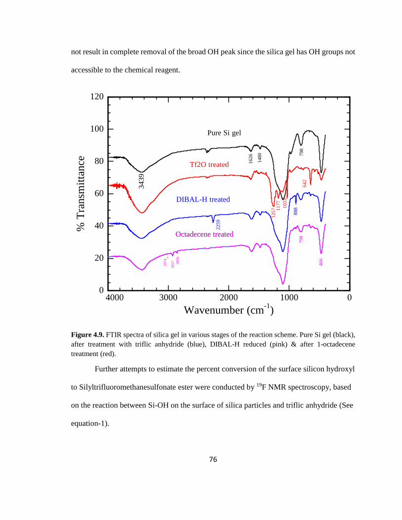
76
not result in complete removal of the broad OH peak since the silica gel has OH groups not
accessible to the chemical reagent.
Figure 4.9. FTIR spectra of silica gel in various stages of the reaction scheme. Pure Si gel (black),
after treatment with triflic anhydride (blue), DIBAL-H reduced (pink) & after 1-octadecene
treatment (red).
Further attempts to estimate the percent conversion of the surface silicon hydroxyl
to Silyltrifluoromethanesulfonate ester were conducted by 19F NMR spectroscopy, based
on the reaction between Si-OH on the surface of silica particles and triflic anhydride (See
equation-1).
01000200030004000
Wavenumber (cm-1
)
0
20
40
60
80
100
120
%T
ran
smit
tan
ce
Pure Si gel
Tf2O treated
DIBAL-H treated
Octadecene treatedOctadecene treatedOctadecene treatedOctadecene treatedOctadecene treated
34
39
1626
1480 798
125
7 1033
1177
642
2259
88
8
29
27
28
56*
297
4
466
798

77
The chemical shifts of methyl fluorine in triflic anhydride (reactant) and triflic acid
(product) occur at -72.6 ppm and -77.3 ppm, respectively. Their integrated peak intensities
allowed determination of the extent of the triflation reaction, assuming that the only source
of triflic acid was from silanol esterification. However, if moisture is present, it can also
hydrolyze the triflic anhydride to give two moles of triflic acid as shown in the following
equation.
Therefore, a control experiment was carried out in a glovebox to examine the effect
of moisture on measurement accuracy. By stirring the triflic anhydride in anhydrous
toluene solvent for 24 and 48 hours at 60 °C, 19F-NMR data showed that the peak
integration ratio of triflic acid to triflic anhydride was 1:148 (or 1:296 wt. mole ratio) and
1:80 (or 1:160 wt. mole ratio), respectively. This indicated that moisture present in
glovebox during triflation reaction was negligible. After 24 and 48 hours of triflation
reaction at 60 °C with 0.2 g of silica gel, this ratio increased to 1:9 and 1:2, respectively
(see Figure 4.10). Based on this, estimated conversion percentage in esterification reaction
was 44 % after 24hours and then reached 100% after 48 hours (by assuming a surface
silanol concentration of 14 mmol/5g silica gel with 4.6 groups SiOH per nm2)106.

78
Figure 4.10. 19F NMR study of silica gel reaction with triflic anhydride. In a control
experiment, a strong peak at -72.6 ppm corresponding to fluorine of triflic anhydride can be
observed. In a reaction with silica gel peak intensity at -77.3 ppm corresponding to triflic
acid increases and reaches to maximum after 48 hours of reaction.
After reduction with DIBAL-H reagent, new peaks in FT-IR appeared at 2259cm-1
and 888 cm-1, which correspond to Si-H stretching, and bending vibrations96; see the pink
curve in Figure 4.9. Note that Si-H frequency depends on the polarity of the other three
bonds with silicon, varying from 2109 to 2250 in going from C-Si-H to O-Si-H107.
Silicon hydride groups (Si-H) were further modified to alkylated silica (Si-R) by
treating with 1-octadecene in the presence of UV light (254nm) for 2 hours108. Samples
were washed with anhydrous chloroform (CHCl3) solvent to remove excess adsorbed 1-
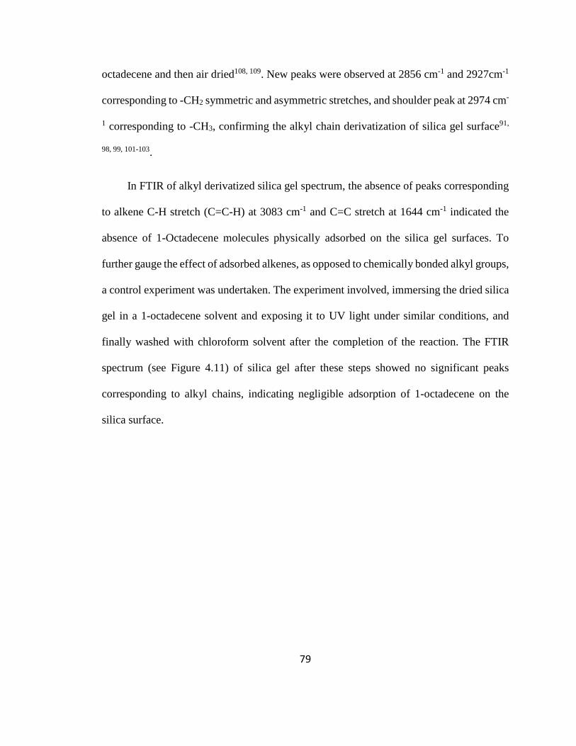
79
octadecene and then air dried108, 109. New peaks were observed at 2856 cm-1 and 2927cm-1
corresponding to -CH2 symmetric and asymmetric stretches, and shoulder peak at 2974 cm-
1 corresponding to -CH3, confirming the alkyl chain derivatization of silica gel surface91,
98, 99, 101-103.
In FTIR of alkyl derivatized silica gel spectrum, the absence of peaks corresponding
to alkene C-H stretch (C=C-H) at 3083 cm-1 and C=C stretch at 1644 cm-1 indicated the
absence of 1-Octadecene molecules physically adsorbed on the silica gel surfaces. To
further gauge the effect of adsorbed alkenes, as opposed to chemically bonded alkyl groups,
a control experiment was undertaken. The experiment involved, immersing the dried silica
gel in a 1-octadecene solvent and exposing it to UV light under similar conditions, and
finally washed with chloroform solvent after the completion of the reaction. The FTIR
spectrum (see Figure 4.11) of silica gel after these steps showed no significant peaks
corresponding to alkyl chains, indicating negligible adsorption of 1-octadecene on the
silica surface.
80
Figure 4.11. FTIR of silica gel control experiment. Comparison of pure silica gel before
reaction and after treatment with 1-Octadecene in the presence of UV light. No peaks
corresponding to alkyl chains can be observed in 2800 to 3000 cm-1 region.
After studying the reaction on organic molecules and heterogeneous silica gel, the
method was tested on a classic SiOx wafer. Reaction progress was studied by FTIR and
water contact angle (CA) measurement.
4.5.4. Results on SiOx wafer reaction
Derivatization studies of SiOx coated wafer provided a suitable comparison with silica gel
(vide supra) and low k CDO (vide infra). These studies utilized silicon wafers decorated

81
with 100 nm thick silicon dioxide treated in identical reaction conditions. A clean SiOx
wafer before the reaction showed the peaks (the black trace in Figure 4.12) corresponding
to the stretching (3376 cm-1 ) and bending vibrations (1296 cm-1) of the silanol (Si-OH);
the symmetric (890 cm-1) and asymmetric stretching (1105 cm-1) of cage Si-O-Si; and the
bending vibration (610 cm-1) of Si-O-Si82. Lower peak intensities associated with O-H
stretch vibrations (at 3500cm-1) when compared to Si-O-Si peaks (at 1100 cm-1), indicated
a lower net content of surface Si-OH groups on SiOx wafer films than silica gel (cf. black
curves in Figures 4.9 and 4.12).
Figure 4.12. FT-IR spectra of SiOx wafer at various stages of the reaction: clean SiOx film
(black); after treatment with triflic anhydride (blue); DIBAL-H reduced (pink); and after
treatment with 1-octadecene (red).

82
The Si-OH absorption peak intensity significantly reduced upon triflation consistent
with the surface accessibility of most Si-OH groups in the nonporous SiOx film(cf. black
and blue traces). After the triflation reaction, new peaks appeared at 1039, 1228 cm-1 and
1193 cm-1 corresponding to symmetric and asymmetric stretches of S=O bond, and C-F
stretch, respectively, as in the case of silica gel. However, their relative peak intensities
were proportionately smaller. After DIBAL-H reduction, the Si-H peak at 2259 cm-1 was
not observed presumably because of the lower total content of SiOH groups on the SiOx
film surface compared to silica gel (cf. pink curves in Figures 4.9 and 4.12). Nevertheless,
silica gel Si-H peaks disappeared upon exposure to air within half an hour. Similarly,
limited stability of the Si-H groups in the air has been previously noted when the remaining
three group bound to silicon are highly polar, such as Si-O.
Hydrosilylation of the hydrogen-terminated Silicon surface with long-chain terminal
alkene was conducted without exposing the sample to atmospheric moisture. After the
photochemical reaction, the presence of peaks at 2853 and 2924 cm-1, corresponding to
CH2 symmetric and asymmetric stretches, and a shoulder peak at 2976 cm-1 (red curve
and red inset in Figure 3) confirmed the hydrosilylation. The ratio of C-H (2800-2950 cm-
1) to Si-O-Si (1100 cm-1) peak intensities was higher than silica gel (cf. Figures 4.9 and
4.12) and could arise from a greater percentage of inaccessible surface SiOH groups in
silica gel. The absence of peaks at 3083 and 1004 cm-1 corresponding to alkene C=C-H
stretching and bending vibrations, and the C=C stretch at 1644 cm-1 of 1-octadecene,
suggested that 1-octadecene was chemically bonded to the silicon surface rather than

83
physically adsorbed. Contact angles before and after derivatization of SiOx surfaces were
11±2o and 101±4o respectively.
4.5.5. Results on CDO wafer reaction
Figure 4.13. Common reaction pathway for hydrogen termination, Octadecane derivatization and
experimental setup of carbon doped silicon oxide (CDO) wafer.
FT-IR, X-ray photoelectron spectroscopy (XPS) and water contact angles (CA)
techniques were employed to monitor the progress of the reaction, and the appearance of
new functional groups on CDO wafer surfaces. When compared to the SiOx wafer the water
contact angle on CDO after RCA clean, was significantly higher (36±3o vs. 11±2o, see
Table 4.2, below) consistent with a more hydrophobic surface due to its higher carbon
content and a lower density of SiOH group on the top surface (cf. black curves in Figures
4.12 and 4.14).
Figure 4.14 shows the transmission FT-IR spectra of a CDO wafer at different stages
of derivatization. Major peaks observed correlated well with the SiOx wafer IR peaks
illustrated in Figure 4.12. However, significantly lower peak intensity in the OH vibrational
frequency range (≈ 3300 cm-1) compared to silica gel or SiOx wafer (Figures 2, 3), implied
a lower net content of OH on the CDO surface. Accordingly, after triflation, intensities of
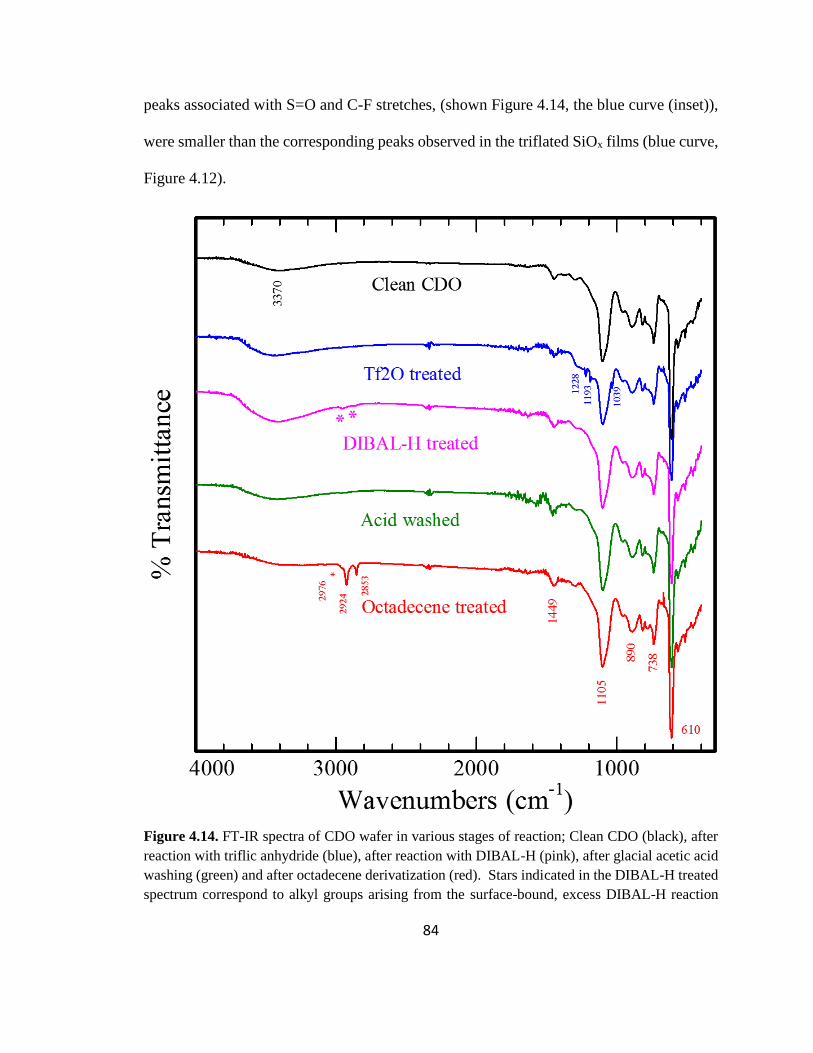
84
peaks associated with S=O and C-F stretches, (shown Figure 4.14, the blue curve (inset)),
were smaller than the corresponding peaks observed in the triflated SiOx films (blue curve,
Figure 4.12).
Figure 4.14. FT-IR spectra of CDO wafer in various stages of reaction; Clean CDO (black), after
reaction with triflic anhydride (blue), after reaction with DIBAL-H (pink), after glacial acetic acid
washing (green) and after octadecene derivatization (red). Stars indicated in the DIBAL-H treated
spectrum correspond to alkyl groups arising from the surface-bound, excess DIBAL-H reaction

85
products. Insets expand selected spectral regions of triflic anhydride Tf2O and octadecene-
derivatized silica in the IR spectra.
Reduction of triflate ester on the CDO surface using DIBAL-H proceeded as in the
case of SiOx 110. After reduction with DIBAL-H several new peaks, not observed in silica
gel or SiOx surfaces, appeared in the range from 2800-3000 cm-1, attributed to alkyl C-H
vibrations. These peaks could originate from traces of the degraded DIBAL-H reagent
(e.g., diisobutyl groups), physically adsorbed or trapped in pores of CDO surface (pink
trace, Figure 4.14). Also, supporting the above hypothesis was an observed increase in the
peak intensity near the OH region (3300 cm-1) due to the formation of Al-OH groups, a
byproduct of the reduction reaction. Since an aluminum oxide or its hydroxide dissolves
readily in an acidic medium, we treated the wafer with 25% glacial acetic acid in anhydrous
toluene for five minutes to remove trapped/ degraded DIBAL-H reagent from the CDO
surface. The FT-IR spectra collected after the acid treatment displayed a reduction in OH
peak intensity and disappearance of alkyl shoulder-peaks (the green trace, Figure 4.14).
A control experiment to further test the hypothesis of DIBAL-H binding on the CDO
surface entailed treating clean CDO, SiOx wafers, and silica gel sample with a DIBAL-H
reagent (see Figure 4.15) in anhydrous toluene. After 24 hours, samples were washed with
dry toluene and dried. Their FT-IR spectra revealed the alkyl peaks only for the CDO
confirming preferential DIBAL-H trapping/adsorption on the surface/pores of a slightly
hydrophobic CDO surface (vide supra) as opposed to hydrophilic surfaces of silica gel or
SiOx wafer.
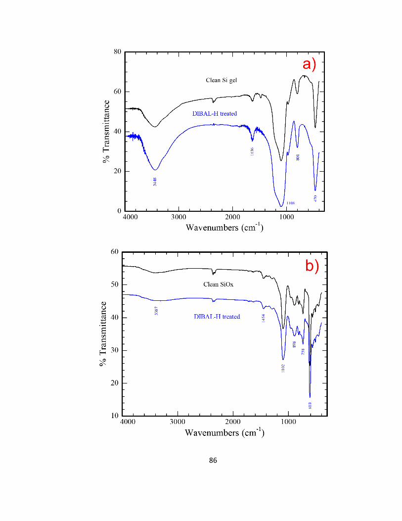
86
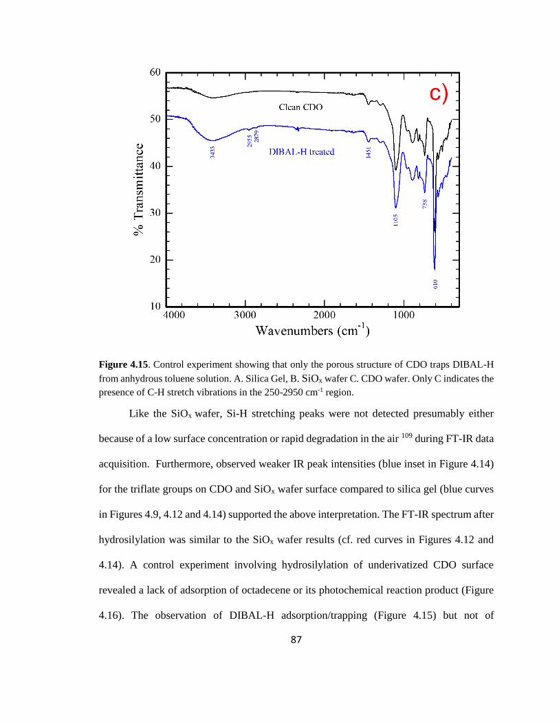
87
Figure 4.15. Control experiment showing that only the porous structure of CDO traps DIBAL-H
from anhydrous toluene solution. A. Silica Gel, B. SiOx wafer C. CDO wafer. Only C indicates the
presence of C-H stretch vibrations in the 250-2950 cm-1 region.
Like the SiOx wafer, Si-H stretching peaks were not detected presumably either
because of a low surface concentration or rapid degradation in the air 109 during FT-IR data
acquisition. Furthermore, observed weaker IR peak intensities (blue inset in Figure 4.14)
for the triflate groups on CDO and SiOx wafer surface compared to silica gel (blue curves
in Figures 4.9, 4.12 and 4.14) supported the above interpretation. The FT-IR spectrum after
hydrosilylation was similar to the SiOx wafer results (cf. red curves in Figures 4.12 and
4.14). A control experiment involving hydrosilylation of underivatized CDO surface
revealed a lack of adsorption of octadecene or its photochemical reaction product (Figure
4.16). The observation of DIBAL-H adsorption/trapping (Figure 4.15) but not of
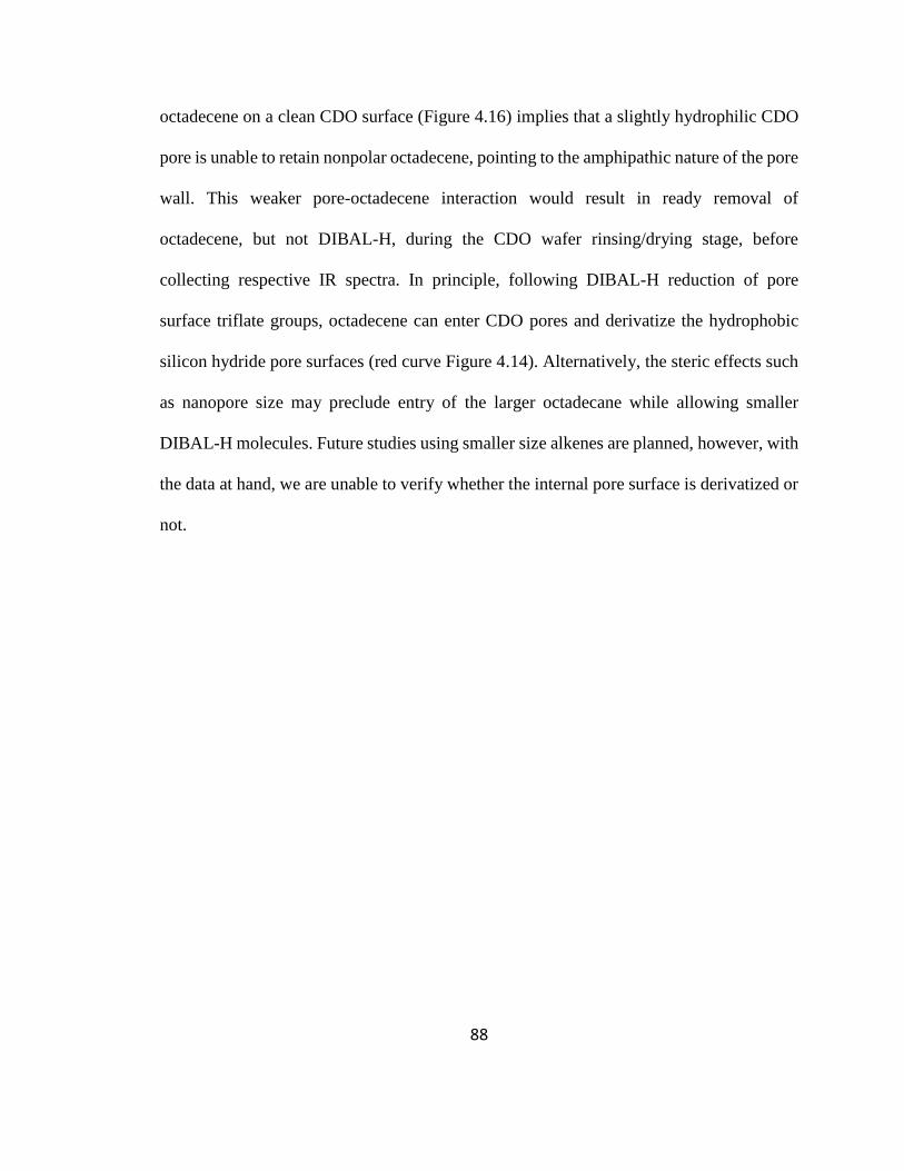
88
octadecene on a clean CDO surface (Figure 4.16) implies that a slightly hydrophilic CDO
pore is unable to retain nonpolar octadecene, pointing to the amphipathic nature of the pore
wall. This weaker pore-octadecene interaction would result in ready removal of
octadecene, but not DIBAL-H, during the CDO wafer rinsing/drying stage, before
collecting respective IR spectra. In principle, following DIBAL-H reduction of pore
surface triflate groups, octadecene can enter CDO pores and derivatize the hydrophobic
silicon hydride pore surfaces (red curve Figure 4.14). Alternatively, the steric effects such
as nanopore size may preclude entry of the larger octadecane while allowing smaller
DIBAL-H molecules. Future studies using smaller size alkenes are planned, however, with
the data at hand, we are unable to verify whether the internal pore surface is derivatized or
not.

89
Figure 4.16. FTIR of CDO wafer control experiment. Spectral comparison of clean CDO, i.e.,
before reaction and CDO after treatment with 1-octadecene in the presence of UV light under
identical conditions, were shown. No peaks corresponding to alkyl chains can be observed in
2800 to 3000 cm-1 region.
A complementary technique of X-ray photoelectron spectroscopy (XPS) provided
further support for derivatization on CDO wafers. Survey spectra obtained from a CDO
surface before (Figure 4.17a) and after (Figure 4.17c) reaction revealed Si, C, and O
elements. After derivatization, the intensity of the carbon (1s) peak increased, consistent
with the derivatization of surface groups with alkyl chains. In deconvoluted high-resolution
Si (2p) spectra of clean CDO wafers before the reaction (Figure 4.17b), three strong peaks
at 101.6, 102.3 and 103.1 eV corresponding to Si-C, -Si-O-C- and -O-Si-O-, respectively
were observed. The XPS spectrum after the reaction (Figure 4.17d) had the same three

90
strong peaks at similar positions but with different intensities. The area of the -O-Si-O-
peak decreased from 26 % to 10 % of the Si (2p) peak area, and the relative area of -Si-C
peak increased from 11 % to 22 %.
Figure 4.17. XPS spectra of CDO wafer. Survey spectrum, a, and Si (2p) high-resolution spectrum,
b, collected before the reaction and c, d are the corresponding spectra collected after the reaction.
This finding validates the conversion of -O-Si-OH to –O-Si-R (R= octadecyl). No
significant change was observed, however, in the peak area for the –Si-O-C- group,
indicating no structural modification in the cage structure of the CDO film. More surface
chemical studies are needed to confirm this indication.

91
Derivatization of the CDO surface with octadecene should change its hydrophobicity.
The contact angle of water droplets deposited on the surface confirmed that shift (Figure
4.18). Clean CDO wafers (Figure 4.18a) had a low contact angle 36±3o caused by the
presence of the hydrophilic hydroxyl groups (Si-OH). Derivatization with octadecene
increased the contact angle to about 81±2o (Figure 4.18b, Table 4.2). The water contact
angles on derivatized surfaces were stable for more than a year (See Figure 4.18) as were
the corresponding IR spectra (Figure 4.19).
Figure 4.18. Water contact angles measured on un-derivatized (clean CDO) and octadecene
derivatized CDO wafers at various time intervals.
Substrate Contact angle
(deg.)
Before reaction (Clean CDO) 36 ± 3°
After reaction 81 ± 2°
9 months later 82 ± 3°
14 months later 82 ± 2°
Table 4.2. Contact angle results of a water droplet on clean CDO and octadecyl derivatized CDO
at various time intervals.
92
Figure 4.19. FTIR spectra comparison of octadecyl derivatized CDO wafer before and after one-
year duration.
4.5.6. Comparison of Octadecyl chains derivatized via DIHAL-H chemistry and Octadecyl
trichlorosilane (OTS) routes
Octadecyltrichlorosilane (OTS), a commonly used silanization agent, readily
forms a self-assembled monolayer on SiOx film transforming it to from hydrophilic to a
hydrophobic surface by inserting an alkoxy ether (Si-O-R) group bearing a C18 alkyl chain.
Hence, the results of octadecene-based vs. the OTS-based derivatization on CDO and SiOx
surfaces were compared. Qualitatively, FT-IR spectra, in the relevant region shown in
Figure 4.20, indicated that the thickness of the hydrocarbon layer is higher for octadecene
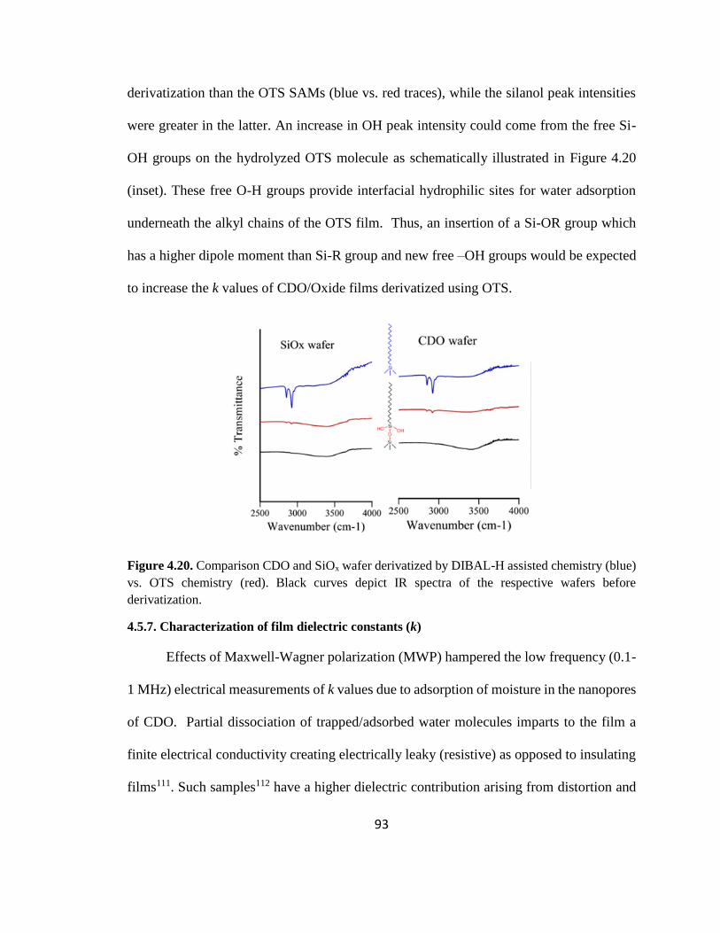
93
derivatization than the OTS SAMs (blue vs. red traces), while the silanol peak intensities
were greater in the latter. An increase in OH peak intensity could come from the free Si-
OH groups on the hydrolyzed OTS molecule as schematically illustrated in Figure 4.20
(inset). These free O-H groups provide interfacial hydrophilic sites for water adsorption
underneath the alkyl chains of the OTS film. Thus, an insertion of a Si-OR group which
has a higher dipole moment than Si-R group and new free –OH groups would be expected
to increase the k values of CDO/Oxide films derivatized using OTS.
Figure 4.20. Comparison CDO and SiOx wafer derivatized by DIBAL-H assisted chemistry (blue)
vs. OTS chemistry (red). Black curves depict IR spectra of the respective wafers before
derivatization.
4.5.7. Characterization of film dielectric constants (k)
Effects of Maxwell-Wagner polarization (MWP) hampered the low frequency (0.1-
1 MHz) electrical measurements of k values due to adsorption of moisture in the nanopores
of CDO. Partial dissociation of trapped/adsorbed water molecules imparts to the film a
finite electrical conductivity creating electrically leaky (resistive) as opposed to insulating
films111. Such samples112 have a higher dielectric contribution arising from distortion and

94
dipolar polarization which raises their effective k113. To disentangle MWP and other
polarization effects require measurements of the film porosity and frequency dependent
dielectric constants as a function of water saturation114 (i.e., humidity). Since these data
were unavailable, a qualitative consideration of capacitance (proportional to k (1MHz))
measurements (Figure 4.21) revealed the following ordering in the magnitude of kOTS >
kCDO > kDIBAL-H, consistent with the expected interfacial polarity of these samples (vide
supra). One way around this problem is to reduce surface SiOH group concentration by
high-temperature baking in an inert environment.
Figure 4.21. Capacitance vs. voltage curves measured using Hg probe method. Hg contact area
was 3.1x10⁻³ cm2. Samples 1, 2 and 3 are underivatized CDO, OTS and Octadecene derivatized
CDO wafers respectively.
Another approach to access k is through measurements of film refractive index;
noting that high frequency (optical) k values simply depend on electronic polarization and
scale as the square of refractive index115. Note, k values at optical frequencies do not
contain dielectric contributions from MWP and dipole polarizations113 (see below).
Analysis of reflectance spectra (Filmetrics) collected from these wafers yielded best-fit
values of refractive index and film thickness; tabulated in Table 4.3. Best-fit refractive

95
index values for CDO films were lower than SiOx films commensurate with the porous
structure of CDO that can trap either water or air, both of which have lower refractive
indices than pure SiO2. Furthermore, the effective refractive index values of OTS
derivatized films were consistently lower than the octadecene derivatized surface implying
perhaps their larger adsorbed moisture content. In either SiOx or CDO films, the refractive
index of DIBAL-H-treated films was greater than the OTS-treated films corresponding to
its thicker hydrocarbon film of the greater refractive index (1.4439) than refractive indices
of either water (1.33) or air (1.0).
To estimate film porosity of CDO crudely, the refractive index of these composite
films (ηexp) was decomposed as a sum of volume fraction (φ) weighted refractive
indices of the constituents116:
where index i denotes a specific component and ϕi its volume fraction. Assuming
that the CDO matrix is made up of SiO2 (ηSiO2 = 1.473) and pores are filled
completely with either air (ηSiO2 = 1), or water (ηH2O = 1.333) gave approximate the
effective porosity of 3 or 11 percent for CDO respectively. Within limits of optical
measurements of the film thickness using filmetrics, the hydrocarbon layer thickness
in the octadecene derivatization scheme was comparable (≈ 5nm) for both CDO and
SiOx (Table 4.3). These values were significantly higher than expected for a densely
packed upright monolayer of C18 chain (2 nm). Ellipsometric measurements,
however, consistently gave a higher thickness of hydrocarbon layer in octadecene
ii
iexp

96
derivatized samples supporting the observed trend of higher IR peak intensities for
the C-H stretch vibrations (Figure 4.20). These higher IR intensities are consistent
with partial cross-linking/polymerization of octadecene during the hydrosilylation
step117.
Table 4.3. Contact angle, film thicknesses of CDO and SiOx wafers.
The contact angle measurements revealed similar trends. The contact angles for
both derivatization schemes depended on the nature film, i.e., CDO vs. SiOx and not
on the chemical mode of derivatization, i.e., silanization vs. hydrosilylation. The
CDO surface which had higher contact angle before derivatization (36o (CDO) vs.
11o (SiOx)) but exhibited lower contact angle after derivatization (87o vs. 91o for
CDO derivatized with octadecene and OTS respectively). Applying the Cassie
equation for a measured contact angle (θm ) on a surface made up of two types of

97
regions (labeled with superscripts 1 and 2) with differing contact angles, θ1 and θ2,
gives118:
2cos)2cos1(coscos fm
where f represents a fraction of the surface of type 1. Crudely, identifying region 1
as SiOx (θ1 = 11o) and region 2 as pores (i.e., air with θ2 = 180o) on the CDO surface,
the estimated upper limit for f = 0.91 implying a 9 percent surface porosity. Should
the lower OH density on the CDO surface be accounted for by setting (θ1 > 11o) the
measured porosity would decrease. For example, if θ1 =30o for the nonporous CDO
surface, then the calculated pore fraction would be 3 percent, similar to the estimates
from the refractive index measurements (Vide Supra). Since we did not have a
nonporous CDO sample, we did not have a value for θ1.
For SiOx surface the observed contact angles after derivation were 101o (octadecene)
vs. 104o (OTS) implying a more densely packed monolayer as was noted
elsewhere119. Again, applying the Cassie equation, but now ascribing region 1 to the
densely packed hydrocarbon monolayer (θ1 = 107o) and region 2 to underivatized
SiOx (θ2 = 11o, from Table 1), estimated f values were 0.97 for OTS and 0.92 for
Octadecene derivatized SiOx surfaces. By contrast, the CDO surface had a thicker
but more loosely packed hydrocarbon layer due to the lower density of surface OH
groups, inferred from its higher initial contact angle. The corresponding f values on
the CDO surfaces were, as expected, smaller; 0.75 (OTS) and 0.69 (Octadecene)
respectively. The results also illustrated that the hydrocarbon layer thickness did
not affect the contact angle, but the areal fraction of derivatized (i.e., f ) surface did.

98
The reaction of hydrofluoric acid (HF) can also enhance the hydrophobicity of the
silicon surface by creating a hydrogen-terminated surface that may be
hydrosilylated, but it would produce undesirable etching of the CDO film. Recently,
our group has used sacrificial silanes to prevent the etching of SiOx by HF. The
chemistry, however, is carried out in an aqueous medium of low pH, which would
likely reoxidize Si-H groups2 and hence is undesirable for this protecting the inner
layer dielectrics from moisture.
4.6. Thiol functionalization of CDO surface to enhance NWs interaction to substrate
Thiol functional groups(-SH) shows strong interaction towards noble and coinage
metals120. Thiol interaction and formation of self-assembled monolayers (SAM) of alkane
thiols on copper has been extensively studied120-123. Thiol functionalization of CDO surface
was explored to enhance the chemical interaction of as-deposited Cu/Ni NWs to CDO
substrate.
Scheme 4.4. Reaction scheme describing thiol functionalization of CDO surface.
Thiol functionalization of CDO was carried out with the DIBAL-H approach, See
Scheme 4.4. The reaction was carried out under identical conditions, except 1-Octadecene
is replaced with a 2-propene thiol in the photochemical reaction. In the FTIR
characterization, 2888 and 2941 cm-1 peaks are attributed to propyl chain (3 carbon chain)

99
and 2564 cm-1 is a characteristic peak corresponding to thiol (-S-H) stretch suggests the
thiol termination, See Figure 4.22.
Figure 4.22. FTIR characterization of as received CDO (black curve) and thiol (-SH)
functionalized CDO (red curve).
Adhesion strength of Cu/Ni NWs to thiol (-SH) functionalized CDO surface: The main
purpose of thiol functionalization is to strongly hold the Cu/Ni NWs after deposition onto
CDO surface. The adhesion strength of as received CDO (non-functionalized) vs. thiol
functionalized CDO was qualitatively assessed by ultra-sonic treatments, see set up in
Figure 4.23a. The procedure involves, drop casting of equal amounts of Cu/Ni NWs

100
solution (250 µL, 5 mg/mL NWs concentration) on as received CDO and thiol-
functionalized CDO (2x2 cm coupons). After drying, wafers substrates were immersed in
ethanol solvent in a beaker and placed in ultrasonicator (160 watts); Figure 4.23a. In case
of non-functionalized CDO, traces of NWs were washed off within 4 seconds of ultrasonic
treatment, see Figure 4.23b. Whereas for thiol functionalized CDO, holds the NWs strongly
till 30 seconds of sonication treatment, see Figure 4.23c. And, after 150 seconds of
ultrasonic treatments traces of NWs were washed off, this suggests the enhanced
interaction of NWs to thiol functionalized CDO surface.
Figure 4.23. Digital photograph showing ultrasonication setup (a), for qualitatively testing the
adhesion strength of Cu/Ni NWs to as received CDO (b), and thiol-functionalized CDO surface (c).

101
4.7. Summary of octadecyl and thiol functionalization
The current plasma treatments to prevent uptake of atmospheric moisture by low
dielectric CDO cause thinning of the films. The classical HMDS derivatization to make
surfaces hydrophobic does not provide sufficient protection. The studies presented here
show a selective derivatization of surface hydrophilic Si-OH groups to form a hydrophobic
alkyl-modified silicon (Si-R, R= -C18H37) without disturbing the rest of the cage structure
of the CDO film. This selective hydrophobic modification should help maintain the ultra-
low k of the insulating film. The method does require an additional processing step to
remove pore-trapped DIBAL-H reagent that can be removed readily with mild acetic acid.
The versatile method allows derivatization of Si-OH functional groups on the surface of
silica gel or CDO wafers with a variety of other organic molecules useful in designing other
biochips, sensors124-126. Preliminary studies indicate that the degree of hydrophobicity
created on surface compares favorably with the classic silanization approach, bypassing
interfacial insertion of the polar Si-O-R group. It provides acceptable thermal processing
stability for the interconnect processing. The same DIBAL-H reduction approach was used
for the thiol (-SH) functionalization. And, the qualitative analysis by ultra-sonic treatments
suggests the strong adhesion of Cu/Ni NWs to the thiol-modified CDO surface.
102
CHAPTER FIVE
NANOWIRES SELF-ASSEMBLY AND ELECTRICAL CHARACTERIZATION
Over the last two decades, substantial efforts have been devoted to the assembly of 1D
nanostructures into nanoscale circuits and interconnects 38, 41-43, 48, 127. In this chapter, the
self-assembly of Cu/Ni NWs into an interconnect structure on a CDO wafer using the
combination of photolithography and magnetic field assisted NWs alignment techniques is
presented. CDO is an important nanoporous low-k material being used as an inner layer
dielectric (ILD) in advanced ultra-large scale integrated circuits (ULSI)60, 128. The NWs
self-assembly protocol discussed here on CDO can also be applied on to the traditional
silicon dioxide (SiOx) substrate.
The Strong interaction between the substrate and deposited NWs is essential for the
successful assembly of NWs129. Here the chemical interaction of thiol (-SH) functional
groups to copper and nickel was exploited to strongly adhere the NWs after deposition onto
the CDO substrate. CDO surface was functionalized with dangling thiol (-SH) functional
groups using the protocol described in chapter 4, section 4.6129, 130. Thiol functionalization
and its characterization were discussed in detail in chapter 4130.
5.1. Self-assembly of Cu/Ni NWs into interconnects
Schematic diagram shown in Figure 5.1 describes the process flow for the fabrication
of Cu/Ni NWs based interconnects. The protocol involves first transferring the desired
circuit pattern (300µm width and 4mm length channel pattern) onto the thiol-functionalized
CDO substrate using a photolithography process, see Section 2.2.5 for more details about
the photolithography process. The above-patterned substrate was placed in between the

103
electromagnet poles like the schematic shown in Figures 3.10 and 5.1. Cu/Ni NWs aqueous
solution (100 µL of 0.5 mg/mL solution) was placed on to the substrate and allowed to dry
in the presence of magnetic field (2500 G). In the presence of magnetic field, NWs oriented
in the applied magnetic field direction and begin to form NW chains in the solution; see
Figure 3.12. After allowing the solvent to dry under ambient conditions, well aligned NWs
deposited on to the surface of photoresist as well as in the thiol-modified trenches on CDO.
The NWs which were deposited in the trenches are strongly held to that surface through
the covalent bond to the thiol functional groups on CDO surface. The NWs which were
deposited on photoresist were loosely bound. These loosely bound NWs and photoresist
were removed by washing with acetone solvent (the so-called lift-off process). Acetone
solvent dissolved the photoresist and simultaneously washed off the loosely bound NWs
from the CDO surface. Finally, the selectively deposited and well-aligned Cu/Ni NWs in
the circuit pattern remained on the substrate like the optical micrographs shown in Figure
5.2.

104
Figure 5.1. Schematic diagram showing a process flow of Cu/Ni NWs self-assembly into
interconnect channels.
Figure 5.2. Optical micrographs of unidirectionally aligned Cu/Ni NWs interconnect channel
fabricated by depositing 0.5 mg/mL of NWs solution on pattern substrate. Inset image in a) shows
digital photograph of 4 mm length and 300 µm width NWs channel with silver ink electrodes on
both ends of the channel.
5.2. Electrical characterization of Cu/Ni NWs based interconnect channels
5.2.1. Effect of nanowire type (pure Cu NWs vs. Cu/Ni NWs) and orientation (random
vs. aligned) on channel resistance.
Electrical characterization studies of as-fabricated NWs channels were carried out
by measuring the electrical resistance using a Keithley-617 programmable digital

105
multimeter. Contact pads on both ends of the interconnect channel were fabricated by
depositing a small amount (20µL) of silver ink, see inset image in Figure 5.2a. The contact
resistance of the dry silver ink was observed as < 1Ω, negligible in comparison to the
resistance of interconnect channels. For the comparison, along with the well-aligned Cu/Ni
NWs deposited in the channel, several samples were fabricated with similar dimensions of
interconnect channels wherein randomly arranged Cu/Ni and pure Cu NWs were deposited.
All the above-fabricated channels used 0.5 mg/mL (dry mass of NWs) concentration of
NWs in aqueous suspensions. The common channel lengths and widths were 4 mm and
300 µm respectively. Schematic diagrams, digital photographs and optical micrographs of
the as mentioned NWs interconnect channels appear in Figures 5.4, 5.4, 5.5 & 5.6.
Figure 5.3. Schematic diagrams and digital photographs showing interconnect channels fabricated
by using different types and arrangement styles of NWs. The random arrangement of Cu NWs
channel in a), unidirectionally aligned Cu/Ni NWs channel in b), and randomly arranged Cu/Ni
NWs channel is shown in c).

106
Figure 5.4. Optical micrographs of Cu NWs based interconnect channel at various magnification
scales showing the random arrangement of Cu NWs.
Figure 5.5. Optical micrographs of Cu/Ni NWs based interconnect channel at various
magnification scales showing directionally well-arranged NWs.

107
Figure 5.6. Optical micrographs of Cu/Ni NWs based interconnect channel at various
magnification scales showing randomly arranged NWs.
Figure 5.7. Plot showing resistance values of well-aligned and randomly arranged Cu/Ni NWs,
and randomly arranged pure Cu NWs based interconnect channels.
The average resistance values of interconnect channels which were made of well-
aligned Cu/Ni NWs, and randomly arranged Cu/Ni NWs and pure Cu NWs were 290 ± 20
kΩ, 780 ± 40 kΩ, and 370 ± 30 kΩ respectively, See Figure 5.7. Average resistance values
and uncertainties were determined by measuring the resistance values of 3 interconnect
0
500
1000
1500
Resis
tan
ce (
k
)
Well aligned Cu/Ni NWs
Random Cu/Ni NWs
Random Cu NWs

108
channels fabricated for each type of NWs arrangement. Lower resistance for well-aligned
Cu/Ni NWs is attributed to the more number of effective conductive channels due to end-
to-end magnetic contacts as illustrated in Figure 5.8.
Figure 5.8. Schematic depicting the randomly aligned Cu/Ni NWs channel fabricated in absence
of magnetic field and orientationally controlled NWs channel fabricated in presence of applied
magnetic field.
High resistance in case of randomly arranged Cu/Ni NWs suggests the percolating
network of NWs leads to a higher number of inter NW hops and effectively a lower number
of effective channels. Whereas for the pure Cu NWs, the resistance is close to the well-
aligned Cu/Ni NWs. This could result from the high conductivity of copper in comparison
to the nickel.
5.2.2. Effect of nanowires alignment order on electrical performance
The above studies reveal the importance of NWs alignment over randomly organized
NWs on achieving a lower channel resistance. For randomly oriented nanowires, the
probability of making interwire contact is uniform over the length of NW while for
magnetized NWs should have a significantly higher probability near its ends56, 131. This
anisotropic sticking probability distribution should be a function of magnetic strength.

109
Thus, the effect of applied magnetic field strength (0-2500 G) on the alignment order and
sample resistance was investigated. Optical micrographs of channels mentioned above
appear in Figure 5.9. As the magnetic field increased, the resistance of NWs channels
decreased, See Figure 5.10. The observation differs in comparison to the other metallic or
carbon nanotube-based results131. This could be attributed to the ferromagnetic nature of
nickel which enhances the end to end NW connections (Figure 5.8) increasing the number
of effective channels formed.
Figure 5.9. Optical microscope images of interconnect channels fabricated at various applied
magnetic field strength from 0 to 2500 Gauss.
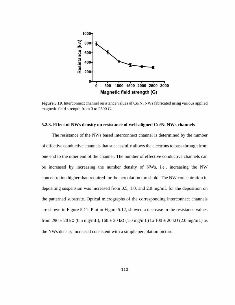
110
Figure 5.10. Interconnect channel resistance values of Cu/Ni NWs fabricated using various applied
magnetic field strength from 0 to 2500 G.
5.2.3. Effect of NWs density on resistance of well-aligned Cu/Ni NWs channels
The resistance of the NWs based interconnect channel is determined by the number
of effective conductive channels that successfully allows the electrons to pass through from
one end to the other end of the channel. The number of effective conductive channels can
be increased by increasing the number density of NWs, i.e., increasing the NW
concentration higher than required for the percolation threshold. The NW concentration in
depositing suspension was increased from 0.5, 1.0, and 2.0 mg/mL for the deposition on
the patterned substrate. Optical micrographs of the corresponding interconnect channels
are shown in Figure 5.11. Plot in Figure 5.12, showed a decrease in the resistance values
from 290 ± 20 kΩ (0.5 mg/mL), 160 ± 20 kΩ (1.0 mg/mL) to 100 ± 20 kΩ (2.0 mg/mL) as
the NWs density increased consistent with a simple percolation picture.
0 500 1000 1500 2000 2500 30000
200
400
600
800
1000
Magnetic field strength (G)
Resis
tan
ce (
kW
)

111
Figure 5.11. Low and high magnification optical micrographs showing of interconnect channels
fabricated by using 0.5 mg/mL, 1.0 mg/mL and 2 mg/mL respectively.
Figure 5.12. Resistance values of Cu/Ni NWs based interconnect channels as a function of NW
concentrations in suspension.
5.2.4. Thermal stability of Cu NWs and Cu/Ni NWs based interconnect channels
The thermal stability of NWs is an important factor for the reliable performance of NWs
based devices. Nickel coated NWs were found to be more oxidation resistant comparison
to pure Cu NWs59. The thermal stability of as-fabricated interconnects channels were
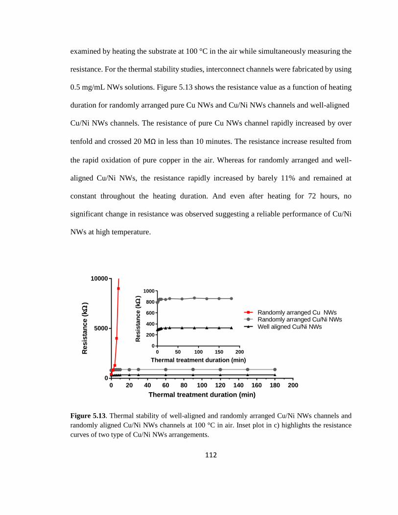
112
examined by heating the substrate at 100 °C in the air while simultaneously measuring the
resistance. For the thermal stability studies, interconnect channels were fabricated by using
0.5 mg/mL NWs solutions. Figure 5.13 shows the resistance value as a function of heating
duration for randomly arranged pure Cu NWs and Cu/Ni NWs channels and well-aligned
Cu/Ni NWs channels. The resistance of pure Cu NWs channel rapidly increased by over
tenfold and crossed 20 MΩ in less than 10 minutes. The resistance increase resulted from
the rapid oxidation of pure copper in the air. Whereas for randomly arranged and well-
aligned Cu/Ni NWs, the resistance rapidly increased by barely 11% and remained at
constant throughout the heating duration. And even after heating for 72 hours, no
significant change in resistance was observed suggesting a reliable performance of Cu/Ni
NWs at high temperature.
Figure 5.13. Thermal stability of well-aligned and randomly arranged Cu/Ni NWs channels and
randomly aligned Cu/Ni NWs channels at 100 °C in air. Inset plot in c) highlights the resistance
curves of two type of Cu/Ni NWs arrangements.
0 20 40 60 80 100 120 140 160 180 2000
5000
10000
Thermal treatment duration (min)
Resis
tan
ce (
k
)
Randomly arranged Cu NWsRandomly arranged Cu/Ni NWsWell aligned Cu/Ni NWs
0 50 100 150 200
0
200
400
600
800
1000
Thermal treatment duration (min)
Resis
tan
ce (
k
)

113
5.3. Summary of Cu/Ni NWs self-assembly and electrical characterization
Despite numerous efforts, there were no successful techniques reported for the large-scale
assembly of copper nanowires. Here, these studies show the potential of the magnetic field
assisted technique to control the orientation and ability to self-assemble the NWs on the
large-scale area. The result was achieved by coating the copper nanowires surface with a
thin layer of ferromagnetic nickel. Electrical characterization results of self-assembled
Cu/Ni NWs channels suggest the importance of orientational alignment for achieving lower
resistance. Also, thermal stability studies reveal Cu/Ni NWs are highly resistant to
oxidation under open-air conditions even at high temperature.

114
CHAPTER SIX
CONCLUSIONS AND FUTURE WORK
6.1. Conclusions
As the on-chip feature sizes are getting smaller, copper filling in the ever-decreasing
channels is getting difficult and reducing the process yield. Therefore, new approaches are
needed to supplement the standard Dual Damascene (DD) process. Fabrication of
interconnects in a bottom-up approach, using 1D nanocrystals as building blocks offers a
potential solution for future high performance integrated circuits. This work demonstrates
a novel and simple solution processable technique to self-assemble the Cu/Ni NWs into
interconnect channels on the low-k material; carbon doped silicon dioxide (CDO).
CDO is a highly nano-porous and hybrid low-k dielectric used in ultra large-scale
integration (ULSI). For the self-assembly process, CDO surface was functionalized with
thiol (-SH) functional groups to bind Cu/Ni NWs. Thiol functionalization was achieved via
a novel approach developed to functionalize selectively the surface exposed hydrophilic
Si-OH groups. Also, the same reaction was used to address the moisture uptake issue of
CDO. In the chip integration process, an oxygen plasma irreversibly changes the silicon
functional groups on the CDO surface from hydrophobic to hydrophilic, which causes an
adverse effect on increasing the k value by taking up moisture. This present work solves
this issue by selectively functionalizing the surface exposed Si-OH functional groups to
hydrophobic octadecyl terminated silicon and helps in maintain the low k value.
In a bottom-up method, dimensionally controlled nanowires synthesis and precisely
controlling the orientation and positioning of NWs are very critical. Here, in a wet synthesis

115
process, reagent concentrations and reaction temperatures were optimized to generate high
aspect ratio and surface morphology controlled Cu NWs. This thesis work developed the
magnetic field assisted technique to control the orientation of Cu/Ni NWs on a large surface
area. Coating a thin layer of ferromagnetic nickel (Ni) onto the Cu NWs surface imparted
magnetic field-mediated alignment of the composite NWs. Furthermore, the nickel coating
helped in protecting the copper core from oxidation.
Finally, Cu/Ni NWs self-assembly into interconnect channels was demonstrated
using the combination of photolithography and magnetic field assisted techniques. The
electrical measurements revealed that well-aligned NWs exhibited less than two-fold lower
resistance than the randomly organized Cu/Ni NWs channels. Also, as the degree of
alignment of the NWs increased, a decrease in resistance was observed. This result is in
stark contrast to the simulations results discussed for other types of NWs (Ag NWs, Au
NWs and CNT). The enhanced performance of the magnetic field assisted alignment
technique appeared to be related to the propensity of end-to-end contacts thereby reducing
an overall number of nanowire contacts for electron transport between the two contacting
electrodes. Furthermore, Cu/Ni NWs showed a higher thermal stability than the pure Cu
NWs, due to their high oxidation resistance. This led to a more reliable electrical
performance under ambient conditions.
6.2. Limitations
One of the important limitation of the as developed technique is, it can only apply to the
ferro/para magnetic nanowires. For non-magnetic nanowires (pure metallic or carbon
nanotubes etc.), they have to be coated with a magnetically active material to give a net

116
alignment when subjected to a modest magnetic field (2000 G). Here, the Cu/Ni NWs self-
assembly process was demonstrated in 300 µm width channels, but the future technology
requires fabrication of ultra-thin (< 5nm) interconnect channels9. For this, the self-
assembly has to be performed with ultra-thin nanowires.
Another area needing improvement is a reduction in the observed high resistance
values of NWs based interconnect channels. The significant contribution to the high
resistance has been attributed to NW to NW junctional resistance131, 132. This nanowire
junction resistance can be minimized by fusing or welding the nanowire contacts either by
thermal or laser ablation techniques131, 132. Also, this technique only demonstrates the NWs
self-assembly in a two-dimensional manner, but it needs to be adopted for the fabrication
of copper vias (vertically aligned NWs which would connect to the two adjacent layers).
Therefore, more efforts are needed to apply the as developed magnetic field assisted self-
assembly technique to fulfill the future interconnect fabrication needs.
6.3. Other applications
Copper nanowires (Cu NWs) and nickel coated Cu NWs (Cu/Ni NWs) have been
successfully demonstrated as an excellent material of choice for the preparation of highly
flexible and transparent electrodes33, 34, 59, 66. In case of Ag NWs, it was demonstrated that
orientationally well-aligned NWs (deposited as a crossed arrays or mesh, like the image
shown in Figure 3.11c), yields high transparency and lower sheet resistance values as
opposed to randomly organized NWs arrays45, 49. Cu/Ni NWs are the better choice than Ag
NWs due to its cheap precursor cost, high oxidation resistance and orientability that can be
well controlled in a large-scale area. Currently, studies of Cu/Ni NWs deposition as a mesh
117
on a polyethylenetetraphthalate (PET) substrate for the application of highly transparent
and flexible devices are underway in our lab.
6.4. Future work
In this work, 300 µm width and 4 mm lengthy channels were used to demonstrate the self-
assembly process. However, one may use the magnetic field assisted technique to assemble
the single NWs based ultra-thin channels. In the literature, researchers have demonstrated
the synthesis of three-atom wide copper nanowires133. The developed magnetic field
assisted self-assembly process is very promising, and perhaps it can be used to fabricate
the three-atom wide interconnect channels which are highly desirable for future
commercial chip fabrication.

118
REFERENCES
1. Barceloux, D. G.; Barceloux, D., Copper. Journal of toxicology: clinical
Toxicology 1999, 37 (2), 217-230.
2. Mistkawi, N. Fundamental Studies in Selective Wet Etching and Corrosion
Processes for High-Performance Semiconductor Devices. Dissertation, Portland State
University, Portland, 2010.
3. Mistry, K.; Allen, C.; Auth, C.; Beattie, B.; Bergstrom, D.; Bost, M.; Brazier, M.;
Buehler, M.; Cappellani, A.; Chau, R. In A 45nm logic technology with high-k+ metal
gate transistors, strained silicon, 9 Cu interconnect layers, 193nm dry patterning, and
100% Pb-free packaging, Electron Devices Meeting, 2007. IEDM 2007. IEEE
International, IEEE: 2007; pp 247-250.
4. IBM IBM's 100 Icons of Progress. http://www-
03.ibm.com/ibm/history/ibm100/us/en/icons/copperchip/.
5. Edelstein, D.; Heidenreich, J.; Goldblatt, R.; Cote, W.; Uzoh, C.; Lustig, N.;
Roper, P.; McDevitt, T.; Motsiff, W.; Simon, A. In Full copper wiring in a sub-0.25/spl
mu/m CMOS ULSI technology, Electron Devices Meeting, 1997. IEDM'97. Technical
Digest., International, IEEE: 1997; pp 773-776.
6. Venkatesan, S.; Gelatos, A.; Misra, V.; Smith, B.; Islam, R.; Cope, J.; Wilson, B.;
Tuttle, D.; Cardwell, R.; Anderson, S., IEEE Int'l Electron Device Meeting Tech. Digest:
1997.
7. Valeev, A.; Krasnikov, G. Y., Manufacturing technology of intra-and interchip
interconnects for modern ULSIs: Review and concepts of development. Russian
Microelectronics 44 (3), 154-172.
8. Waveforms, P., Overview of the Use of Copper Interconnects in the
Semiconductor Industry. Technology 2001, 2003, 2005.
9. Brain, R. In Interconnect scaling: Challenges and opportunities, Electron Devices
Meeting (IEDM), 2016 IEEE International, IEEE: pp 9.3. 1-9.3. 4.

119
10. Perry, K. A. In Chemical mechanical polishing: The impact of a new technology
on an industry, VLSI Technology, 1998. Digest of Technical Papers. 1998 Symposium
on, IEEE: 1998; pp 2-5.
11. Baklanov, M. R.; Adelmann, C.; Zhao, L.; De Gendt, S., Advanced Interconnects:
Materials, Processing, and Reliability. ECS Journal of Solid State Science and
Technology 4 (1), Y1-Y4.
12. Wetzig, K.; Wendrock, H.; Buerke, A.; Kotter, T. In In-situ study of interconnect
failures by electromigration inside a scanning electron microscope, AIP Conference
Proceedings, AIP: 1999; pp 89-99.
13. Cho, J.; Thompson, C., Grain size dependence of electromigration induced
failures in narrow interconnects. Applied Physics Letters 1989, 54 (25), 2577-2579.
14. Bower, A.; Craft, D., Analysis of failure mechanisms in the interconnect lines of
microelectronic circuits. Fatigue & fracture of engineering materials &
structures 1998, 21 (5), 611-630.
15. Fischer, A.; Von Glasow, A.; Penka, S.; Ungar, F. In Electromigration failure
mechanism studies on copper interconnects, Interconnect Technology Conference, 2002.
Proceedings of the IEEE 2002 International, IEEE: 2002; pp 139-141.
16. Vairagar, A.; Mhaisalkar, S.; Meyer, M.; Zschech, E.; Krishnamoorthy, A.; Tu,
K.; Gusak, A., Direct evidence of electromigration failure mechanism in dual-damascene
Cu interconnect tree structures. Applied Physics Letters 2005, 87 (8), 081909.
17. Xu, W.-H.; Wang, L.; Guo, Z.; Chen, X.; Liu, J.; Huang, X.-J., Copper Nanowires
as Nanoscale Interconnects: Their Stability, Electrical Transport, and Mechanical
Properties. ACS nano 9 (1), 241-250.
18. Jason, N. N.; Shen, W.; Cheng, W., Copper Nanowires as Conductive Ink for
Low-Cost Draw-On Electronics. ACS Applied Materials & Interfaces 7 (30), 16760-
16766.
19. Kovtyukhova, N. I.; Mallouk, T. E., Nanowires as Building Blocks for
Self―Assembling Logic and Memory Circuits. Chemistry-A European Journal 2002, 8
(19), 4354-4363.

120
20. Xu, W.; Yu, S. H., Conducting performance of individual Ag@ C coaxial
nanocables: ideal building blocks for interconnects in nanoscale devices. Small 2009, 5
(4), 460-465.
21. Mohl, M.; Pusztai, P.; Kukovecz, A.; Konya, Z.; Kukkola, J.; Kordas, K.; Vajtai,
R.; Ajayan, P. M., Low-Temperature Large-Scale Synthesis and Electrical Testing of
Ultralong Copper Nanowires. Langmuir 26 (21), 16496-16502.
22. Yao, Z.; Kane, C. L.; Dekker, C., High-field electrical transport in single-wall
carbon nanotubes. Physical Review Letters 2000, 84 (13), 2941.
23. Gao, M. R.; Xu, W. H. H.; L.B., L.; Zhan, Y. J.; Yu, S. H., Coaxial Metal
Nano/Microcables with Isolating Sheath: Synthetic Methodology and Their Application
as Interconnects. Advanced Materials 22 (17), 1977-1981.
24. Wang, C.; Hu, Y.; Lieber, C. M.; Sun, S., Ultrathin Au nanowires and their
transport properties. Journal of the American Chemical Society 2008, 130 (28), 8902-
8903.
25. Critchley, K.; Khanal, B. P.; Marcin G.A. Vigderman, L.; Evans, S. D.; Zubarev,
E. R.; Kotov, N. A., Near Bulk Conductivity of Gold Nanowires as Nanoscale
Interconnects and the Role of Atomically Smooth Interface. Advanced Materials 22 (21),
2338-2342.
26. Molares, M. T.; Hohberger, E. M.; Schaeflein, C.; Blick, R. H.; Neumann, R.;
Trautmann, C., Electrical characterization of electrochemically grown single copper
nanowires. Applied Physics Letters 2003, 82 (13), 2139-2141.
27. Zach, M. P.; Ng, K. H.; Penner, R. M., Molybdenum nanowires by
electrodeposition. Science 2000, 290 (5499), 2120-2123.
28. Marzi, G. D.; Iacopino, D.; Quinn, A.; Redmond, G., Probing intrinsic transport
properties of single metal nanowires: direct-write contact formation using a focused ion
beam. Journal of Applied Physics 2004, 96, 3458-3462.
29. Kim, T.-H.; Zhang, X.-G.; Nicholson, D. M.; Evans, B. M.; Kulkarni, N. S.;
Radhakrishnan, B.; Kenik, E. A.; Li, A.-P., Large discrete resistance jump at grain
boundary in copper nanowire. Nano letters 10 (8), 3096-3100.
121
30. Tanase, M.; Silevitch, D.; Hultgren, A.; Bauer, L.; Searson, P.; Meyer, G.; Reich,
D., Magnetic trapping and self-assembly of multicomponent nanowires. Journal of
Applied Physics 2002, 91 (10), 8549-8551.
31. Mehta, R.; Chugh, S.; Chen, Z., Enhanced electrical and thermal conduction in
graphene-encapsulated copper nanowires. Nano letters 15 (3), 2024-2030.
32. Li, J.; Ye, Q.; Cassell, A.; Ng, H. T.; Stevens, R.; Han, J.; Meyyappan, M.,
Bottom-up approach for carbon nanotube interconnects. Applied Physics Letters 2003, 82
(15), 2491-2493.
33. Ye, S.; Rathmell, A. R.; Stewart, I. E.; Ha, Y.-C.; Wilson, A. R.; Chen, Z.; Wiley,
B. J., A rapid synthesis of high aspect ratio copper nanowires for high-performance
transparent conducting films. Chemical Communications 50 (20), 2562-2564.
34. Rathmell, A. R.; Wiley, B. J., The synthesis and coating of long, thin copper
nanowires to make flexible, transparent conducting films on plastic substrates. Advanced
Materials 23 (41), 4798-4803.
35. Ye, S.; Stewart, I. E.; Chen, Z.; Li, B.; Rathmell, A. R.; Wiley, B. J., How Copper
Nanowires Grow and How To Control Their Properties. Accounts of chemical research
49 (3), 442-451.
36. Raciti, D.; Livi, K. J.; Wang, C., Highly dense Cu nanowires for low-
overpotential CO2 reduction. Nano Letters 15 (10), 6829-6835.
37. Ryan, J. G.; Geffken, R. M.; Poulin, N. R.; Paraszczak, J. R., The evolution of
interconnection technology at IBM. Ibm Journal of Research and Development 1995, 39
(4), 371-381.
38. Wang, M. C. P.; Gates, B. D., Directed assembly of nanowires. Materials Today
2009, 12 (5), 34-43.
39. Tamhane, K. Formation of lyotropic liquid crystals through the self-assembly of
bile acid building blocks. University of Central Florida Orlando, Florida, 2009.
40. Murali, S.; Xu, T.; Marshall, B. D.; Kayatin, M. J.; Pizarro, K.; Radhakrishnan, V.
K.; Nepal, D.; Davis, V. A., Lyotropic liquid crystalline self-assembly in dispersions of
silver nanowires and nanoparticles. Langmuir 26 (13), 11176-11183.

122
41. Liu, J.-W.; Liang, H.-W.; Yu, S.-H., Macroscopic-Scale Assembled Nanowire
Thin Films and Their Functionalities. Chemical Reviews 112 (8), 4770-4799.
42. Lu, W.; Lieber, C. M., Nanoelectronics from the bottom up. Nature materials
2007, 6 (11), 841-850.
43. Lieber, C. M., Nanoscale science and technology: building a big future from small
things. MRS bulletin 2003, 28 (07), 486-491.
44. Tao, A.; Kim, F.; Hess, C.; Goldberger, J.; He, R.; Sun, Y.; Xia, Y.; Yang, P.,
Langmuir-Blodgett silver nanowire monolayers for molecular sensing using surface-
enhanced Raman spectroscopy. Nano Letters 2003, 3 (9), 1229-1233.
45. Cho, S.; Kang, S.; Pandya, A.; Shanker, R.; Khan, Z.; Lee, Y.; Park, J.; Craig, S.
L.; Ko, H., Large-Area Cross-Aligned Silver Nanowire Electrodes for Flexible,
Transparent, and Force-Sensitive Mechanochromic Touch Screens. ACS nano 11 (4),
4346-4357.
46. Li, D.; Wang, Y.; Xia, Y., Electrospinning of Polymeric and Ceramic Nanofibers
as Uniaxially Aligned Arrays. Nano Letters 2003, 3 (8), 1167-1171.
47. Smith, P. A.; Nordquist, C. D.; Jackson, T. N.; Mayer, T. S.; Martin, B. R.;
Mbindyo, J.; Mallouk, T. E., Electric-field assisted assembly and alignment of metallic
nanowires. Applied Physics Letters 2000, 77 (9), 1399-1401.
48. Kim, Y. L.; Li, B.; An, X.; Hahm, M. G.; Chen, L.; Washington, M.; Ajayan, P.;
Nayak, S. K.; Busnaina, A.; Kar, S., Highly aligned scalable platinum-decorated single-
wall carbon nanotube arrays for nanoscale electrical interconnects. ACS nano 2009, 3 (9),
2818-2826.
49. Yang, Y.; Wang, J.-L.; Liu, L.; Wang, Z.-H.; Liu, J.-W.; Yu, S.-H., A room-
temperature environmentally friendly solution process to assemble silver nanowire
architectures for flexible transparent electrodes. Nanoscale 9 (1), 52-55.
50. Ye, H.; Gu, Z.; Yu, T.; Gracias, D. H., Integrating nanowires with substrates
using directed assembly and nanoscale soldering. IEEE Transactions on nanotechnology
2006, 5 (1), 62-66.
51. Hangarter, C. M.; Myung, N. V., Magnetic alignment of nanowires. Chemistry of
materials 2005, 17 (6), 1320-1324.

123
52. Fan, Z.; Ho, J. C.; Jacobson, Z. A.; Yerushalmi, R.; Alley, R. L.; Razavi, H.;
Javey, A., Wafer-scale assembly of highly ordered semiconductor nanowire arrays by
contact printing. Nano Letters 2008, 8 (1), 20-25.
53. Choi, H.; Park, S.-H., Seedless growth of free-standing copper nanowires by
chemical vapor deposition. Journal of the American Chemical Society 2004, 126 (20),
6248-6249.
54. Barako, M. T.; Roy-Panzer, S.; English, T. S.; Kodama, T.; Asheghi, M.; Kenny,
T. W.; Goodson, K. E., Thermal conduction in vertically aligned copper nanowire arrays
and composites. ACS applied materials & interfaces 7 (34), 19251-19259.
55. Zhou, R.; Chang, H.-C.; Protasenko, V.; Kuno, M.; Singh, A. K.; Jena, D.; Xing,
H., CdSe nanowires with illumination-enhanced conductivity: Induced dipoles,
dielectrophoretic assembly, and field-sensitive emission. Journal of Applied Physics
2007, 101 (7), 073704.
56. Yoo, B.; Rheem, Y.; Beyermann, W. P.; Myung, N. V., Magnetically assembled
30 nm diameter nickel nanowire with ferromagnetic electrodes. Nanotechnology 2006, 17
(10), 2512.
57. Chen, H.; Lee, J.-H.; Kim, Y.-H.; Shin, D.-W.; Park, S.-C.; Meng, X.; Yoo, J.-B.,
Metallic copper nanostructures synthesized by a facile hydrothermal method. Journal of
nanoscience and nanotechnology 10 (1), 629-636.
58. Chang, Y.; Lye, M. L.; Zeng, H. C., Large-scale synthesis of high-quality
ultralong copper nanowires. Langmuir 2005, 21 (9), 3746-3748.
59. Rathmell, A. R.; Nguyen, M.; Chi, M.; Wiley, B. J., Synthesis of oxidation-
resistant cupronickel nanowires for transparent conducting nanowire networks. Nano
Letters 12 (6), 3193-3199.
60. Darmakkolla, S. R.; Tran, H.; Gupta, A.; Rananavare, S. B., A method to
derivatize surface silanol groups to Si-alkyl groups in carbon-doped silicon oxides. RSC
Advances 6 (95), 93219-93230.
61. Andideh, E.; Peterson, K. L., Method of forming a carbon doped oxide layer on a
substrate. Google Patents: 2002.

124
62. Chang, T. C.; Mor, Y. S.; Liu, P. T.; Tsai, T. M.; Chen, C. W.; Mei, Y. J.; Sze, S.
M., Recovering dielectric loss of low dielectric constant organic siloxane during the
photoresist removal process. Journal of the Electrochemical Society 2002, 149 (8), F81-
F84.
63. Humphreys, F.; Brough, I., High resolution electron backscatter diffraction with a
field emission gun scanning electron microscope. Journal of microscopy 1999, 195 (Pt
1), 6-9.
64. Trimby, P. W., Orientation mapping of nanostructured materials using
transmission Kikuchi diffraction in the scanning electron microscope. Ultramicroscopy
120, 16-24.
65. Keller, R. R.; Geiss, R. H., Transmission EBSD from 10 nm domains in a
scanning electron microscope. Journal of microscopy 245 (3), 245-251.
66. Rathmell, A. R.; Bergin, S. M.; Hua, Y. L.; Li, Z. Y.; Wiley, B. J., The growth
mechanism of copper nanowires and their properties in flexible, transparent conducting
films. Advanced Materials 22 (32), 3558-3563.
67. Tung, H.-T.; Song, J.-M.; Dong, T.-Y.; Hwang, W.-S.; Chen, I.-G., Synthesis of
Surfactant-free Aligned Single Crystal Copper Nanowires by Thermal-Assisted
Photoreduction. Crystal Growth & Design 2008, 8 (9), 3415-3419.
68. Meng, F.; Jin, S., The solution growth of copper nanowires and nanotubes is
driven by screw dislocations. Nano letters 12 (1), 234-239.
69. Kim, M. J.; Flowers, P. F.; Stewart, I. E.; Ye, S.; Baek, S.; Kim, J. J.; Wiley, B. J.,
Ethylenediamine Promotes Cu Nanowire Growth by Inhibiting Oxidation of Cu (111).
Journal of the American Chemical Society 139 (1), 277-284.
70. Niu, Z.; Li, Y., Removal and utilization of capping agents in nanocatalysis.
Chemistry of materials 26 (1), 72-83.
71. Ye, S.; Rathmell, A. R.; Ha, Y. C.; Wilson, A. R.; Wiley, B. J., The Role of
Cuprous Oxide Seeds in the One Pot and Seeded Syntheses of Copper Nanowires. Small
10 (9), 1771-1778.

125
72. Stewart, I. E.; Ye, S.; Chen, Z.; Flowers, P. F.; Wiley, B. J., Synthesis of Cu-Ag,
Cu-Au, and Cu-Pt core-shell nanowires and their use in transparent conducting films.
Chemistry of Materials 27 (22), 7788-7794.
73. Li, J.; Shacham-Diamand, Y.; Mayer, J. W., Copper deposition and thermal
stability issues in copper-based metallization for ULSI technology. Materials science
reports 1992, 9 (1), 1-51.
74. Murarka, S. P.; Hymes, S. W., Copper metallization for ULSL and beyond.
Critical Reviews in Solid State and Material Sciences 1995, 20 (2), 87-124.
75. Venkatesan, S.; Gelatos, A.; Hisra, S.; Smith, B.; Islam, R.; Cope, J.; Wilson, B.;
Tuttle, D.; Cardwell, R.; Anderson, S. In A high performance 1.8 V, 0.20/spl mu/m
CMOS technology with copper metallization, Electron Devices Meeting, 1997. IEDM'97.
Technical Digest., International, IEEE: 1997; pp 769-772.
76. Jing, S.-Y.; Lee, H.-J.; Choi, C. K., Chemical bond structure on Si-OC composite
films with a low dielectric constant deposited by using inductively coupled plasma
chemical vapor deposition. Journal of the Korean Physical Society 2002, 41 (5), 769-773.
77. Kim, J. H.; Seo, S. H.; Yun, S. M.; Chang, H. Y.; Lee, K. M.; Choi, C. K., The
deposition of SiOF film with low dielectric constant in a helicon plasma source. Applied
Physics Letters 1996, 68 (11), 1507-1509.
78. Kim, J. H.; Seo, S. H.; Yun, S. M.; Chang, H. Y.; Lee, K. M.; Choi, C. K., A
study on low dielectric material deposition using a helicon plasma source. Journal of the
Electrochemical Society 1996, 143 (9), 2990-2995.
79. Grill, A.; Patel, V., Ultralow-k dielectrics prepared by plasma-enhanced chemical
vapor deposition. Applied Physics Letters 2001, 79 (6), 803-805.
80. Grill, A.; Patel, V., Low dielectric constant films prepared by plasma-enhanced
chemical vapor deposition from tetramethylsilane. Journal of Applied Physics 1999, 85
(6), 3314-3318.
81. Fujii, T.; Hiramatsu, M.; Nawata, M., Formation of Si-based organic thin films
with low dielectric constant by using remote plasma enhanced chemical vapor deposition
from hexamethyldisiloxane. Thin Solid Films 1999, 343, 457-460.

126
82. Grill, A.; Neumayer, D. A., Structure of low dielectric constant to extreme low
dielectric constant SiCOH films: Fourier Transform infrared spectroscopy
characterization. Journal of Applied Physics 2003, 94 (10), 6697-6707.
83. Yang, C. S.; Yu, Y. H.; Lee, K.-M.; Lee, H.-J.; Choi, C. K., Investigation of low
dielectric carbon-doped silicon oxide films prepared by PECVD using
methyltrimethoxysilane precursor. Thin Solid Films 2006, 506, 50-54.
84. Han, Q.; Chen, W.; Waldfried, C.; Escorcia, O.; Sbrockey, N.; Bridgewater, T.;
Moyer, E.; Berry, I. In Ultra low-k porous silicon dioxide films from a plasma process,
Interconnect Technology Conference, 2001. Proceedings of the IEEE 2001 International,
IEEE: 2001; pp 171-173.
85. Wang, Y. H.; Kumar, R.; Zhou, X.; Pan, J. S.; Chai, J. W., Effect of oxygen
plasma treatment on low dielectric constant carbon-doped silicon oxide thin films. Thin
Solid Films 2005, 473 (1), 132-136.
86. Reichelderfer, R. F.; Welty, J. M.; Battey, J. F., The Ultimate By-Products of
Stripping Photoresist in an Oxygen Plasma. Journal of the Electrochemical Society 1977,
124 (12), 1926-1927.
87. Chang, T. C.; Chen, C. W.; Liu, P. T.; Mor, Y. S.; Tsai, H. M.; Tsai, T. M.; Yan,
S. T.; Tu, C. H.; Tseng, T. Y.; Sze, S. M., Moisture-induced material instability of porous
organosilicate glass. Electrochemical and Solid State Letters 2003, 6 (4), F13-F15.
88. Liu, P. T.; Chang, T. C.; Su, H.; Mor, Y. S.; Yang, Y. L.; Chung, H.; Hou, J.; Sze,
S. M., Improvement in integration issues for organic low-k hybrid-organic-siloxane-
polymer. Journal of the Electrochemical Society 2001, 148 (2), F30-F34.
89. Wang, Z.; Catabay, W. G.; Zhao, J. W., Process for treating damaged surfaces of
low dielectric constant organo silicon oxide insulation material to inhibit moisture
absorption. Google Patents: 2000.
90. Le, Q. T.; Baklanov, M.; Kesters, E.; Azioune, A.; Struyf, H.; Boullart, W.;
Pireaux, J.-J.; Vanhaelemeersch, S., Removal of plasma-modified low-k layer using
dilute HF: Influence of concentration. Electrochemical and Solid-State Letters 2005, 8
(7), F21-F24.

127
91. An, D.; Wang, Z.; Zhao, X.; Liu, Y.; Guo, Y.; Ren, S., A new route to synthesis
of surface hydrophobic silica with long-chain alcohols in water phase. Colloids and
Surfaces a-Physicochemical and Engineering Aspects 2010, 369 (1-3), 218-222.
92. Rao, C. N. R.; Muller, A.; Cheetham, A. K., The chemistry of nanomaterials:
synthesis, properties and applications. John Wiley & Sons: 2006; Vol. 1.
93. Gurav, J. L.; Jung, I.-K.; Park, H.-H.; Kang, E. S.; Nadargi, D. Y., Silica aerogel:
synthesis and applications. Journal of Nanomaterials 2010, 23.
94. Dorcheh, A. S.; Abbasi, M. H., Silica aerogel; synthesis, properties and
characterization. Journal of Materials Processing Technology 2008, 199 (1-3), 10-26.
95. Gurav, J. L.; Jung, I.-K.; Park, H.-H.; Kang, E. S.; Nadargi, D. Y., Silica Aerogel:
Synthesis and Applications. Journal of Nanomaterials 2010.
96. Ashu-Arrah, B. A.; Glennon, J. D.; Albert, K., Preparation and characterization of
bonded silica hydride intermediate from triethoxysilane and dimethylmethoxysilane using
supercritical carbon dioxide and dioxane as reaction medium. Journal of
Chromatography A 2012, 1236, 42-50.
97. Jal, P. K.; Patel, S.; Mishra, B., Chemical modification of silica surface by
immobilization of functional groups for extractive concentration of metal ions. Talanta
2004, 62 (5), 1005-1028.
98. Kartal, A. M.; Erkey, C., Surface modification of silica aerogels by
hexamethyldisilazane-carbon dioxide mixtures and their phase behavior. The Journal of
Supercritical Fluids 2010, 53 (1), 115-120.
99. Suratwala, T. I.; Hanna, M. L.; Miller, E. L.; Whitman, P. K.; Thomas, I. M.;
Ehrmann, P. R.; Maxwell, R. S.; Burnham, A. K., Surface chemistry and trimethylsilyl
functionalization of Stober silica sols. Journal of Non-Crystalline Solids 2003, 316 (2-3),
349-363.
100. Zareyee, D.; Karimi, B., A novel and highly efficient method for the silylation of
alcohols with hexamethyldisilazane (HMDS) catalyzed by recyclable sulfonic acid-
functionalized ordered nanoporous silica. Tetrahedron Letters 2007, 48 (7), 1277-1280.

128
101. Nadargi, D. Y.; Gurav, J. L.; El Hawi, N.; Rao, A. V.; Koebel, M., Synthesis and
characterization of transparent hydrophobic silica thin films by single step sol-gel process
and dip coating. Journal of Alloys and Compounds 2010, 496 (1-2), 436-441.
102. Shewale, P. M.; Rao, A. V.; Rao, A. P., Effect of different trimethyl silylating
agents on the hydrophobic and physical properties of silica aerogels. Applied Surface
Science 2008, 254 (21), 6902-6907.
103. Rao, A. V.; Kulkarni, M. M.; Amalnerkar, D. P.; Seth, T., Surface chemical
modification of silica aerogels using various alkyl-alkoxy/chloro silanes. Applied Surface
Science 2003, 206 (1-4), 262-270.
104. Mhaisagar, Y. S.; Joshi, B. N.; Mahajan, A. M., Mechanical properties of surface
modified silica low-k thin films. Microelectronic Engineering 2014, 114, 112-116.
105. Zhuravlev, L. T., Concentration of hydroxyl-groups on the surface of amorphous
silicas. Langmuir 1987, 3 (3), 316-318.
106. Sandoval, J. E.; Pesek, J. J., Synthesis and characterization of a hydride -modified
porous silica material as an intermediate in the preparation of chemically bonded
chromatographic stationary phases. Analytical Chemistry 1989, 61 (18), 2067-2075.
107. Voronkov, M. G.; Pukhnarevich, V. B., Properties and transformations of the Si-
H bonds in organosilicon compounds. Bulletin of the Academy of Sciences of the USSR,
Division of chemical science 1982, 31 (5), 939-957.
108. Buriak, J. M., Organometallic chemistry on silicon and germanium surfaces.
Chemical Reviews 2002, 102 (5), 1271-1308.
109. Wayner, D. D. M.; Wolkow, R. A., Organic modification of hydrogen terminated
silicon surfaces. Journal of the Chemical Society-Perkin Transactions 2 2002, (1), 23-34.
110. Tour, J. M.; John, J. A.; Stephens, E. B., Convenient route to diorganosilyl and
triorganosilyl ethy ethers and the corresponding diorganosilanes and triorganosilanes.
Journal of Organometallic Chemistry 1992, 429 (3), 301-310.
111. Anderson Jr, J. H.; Parks, G. A., Electrical conductivity of silica gel in the
presence of adsorbed water. The Journal of Physical Chemistry 1968, 72 (10), 3662-
3668.

129
112. Sakamoto, T.; Nakamura, H.; Uedaira, H.; Wada, A., High-frequency dielectric
relaxation of water bound to hydrophilic silica gels. The Journal of Physical Chemistry
1989, 93 (1), 357-366.
113. Knight, R. J.; Nur, A., The dielectric constant of sandstones, 60 kHz to 4 MHz.
Geophysics 1987, 52 (5), 644-654.
114. Friedman, S. P., A saturation degree-dependent composite spheres model for
describing the effective dielectric constant of unsaturated porous media. Water Resources
Research 1998, 34 (11), 2949-2961.
115. Afsar, M. N.; Button, K. J., Precise Millimeter-Wave Measurements of Complex
Refractive Index, Complex Dielectric Permittivity and Loss Tangent of GaAs, Si,
SiO/sub 2/, A1/sub 2/O/sub 3/, BeO, Macor, and Glass. IEEE Transactions on
Microwave Theory and Techniques 1983, 31 (2), 217-223.
116. Reis, J. C. R.; Lampreia, I. M. S.; Santos, Â. F. S.; Moita, M. L. C. J.; Douhéret,
G., Refractive Index of Liquid Mixtures: Theory and Experiment. ChemPhysChem 11
(17), 3722-3733.
117. de Smet, L. C.; Zuilhof, H.; Sudholter, E. J.; Lie, L. H.; Houlton, A.; Horrocks, B.
R., Mechanism of the hydrosilylation reaction of alkenes at porous silicon: experimental
and computational deuterium labeling studies. The Journal of Physical Chemistry B
2005, 109 (24), 12020-12031.
118. Cassie, A., Contact angles. Discussions of the Faraday Society 1948, 3, 11-16.
119. Koga, T.; Morita, M.; Ishida, H.; Yakabe, H.; Sasaki, S.; Sakata, O.; Otsuka, H.;
Takahara, A., Dependence of the molecular aggregation state of octadecylsiloxane
monolayers on preparation methods. Langmuir 2005, 21 (3), 905-910.
120. Love, J. C.; Estroff, L. A.; Kriebel, J. K.; Nuzzo, R. G.; Whitesides, G. M., Self-
assembled monolayers of thiolates on metals as a form of nanotechnology. Chemical
Reviews 2005, 105 (4), 1103-1170.
121. Jennings, G. K.; Munro, J. C.; Yong, T.-H.; Laibinis, P. E., Effect of chain length
on the protection of copper by n-alkanethiols. Langmuir 1998, 14 (21), 6130-6139.

130
122. Jennings, G. K.; Laibinis, P. E., Self-assembled monolayers of alkanethiols on
copper provide corrosion resistance in aqueous environments. Colloids and Surfaces A:
Physicochemical and Engineering Aspects 1996, 116 (1-2), 105-114.
123. Gelves, G. A.; Sundararaj, U.; Haber, J. A., Electrostatically dissipative
polystyrene nanocomposites containing copper nanowires. Macromolecular rapid
communications 2005, 26 (21), 1677-1681.
124. Chaparadza, A.; Rananavare, S. B., Room temperature Cl 2 sensing using thick
nanoporous films of Sb-doped SnO 2. Nanotechnology 2008, 19 (24), 245501.
125. Chan, J. C.; Hannah-Moore, N.; Rananavare, S. B., Controlled Deposition of Tin
Oxide and Silver Nanoparticles Using Microcontact Printing. Crystals 2015, 5 (1), 116-
142.
126. Jonkheijm, P.; Weinrich, D.; Schroder, H.; Niemeyer, C. M.; Waldmann, H.,
Chemical strategies for generating protein biochips. Angewandte Chemie International
Edition 2008, 47 (50), 9618-9647.
127. Tallapally, V.; Esteves, R. J. A.; Nahar, L.; Arachchige, I. U., Multivariate
Synthesis of Tin Phosphide Nanoparticles: Temperature, Time, and Ligand Control of
Size, Shape, and Crystal Structure. Chemistry of Materials 28 (15), 5406-5414.
128. Grill, A., Amorphous carbon based materials as the interconnect dielectric in
ULSI chips. Diamond and related materials 2001, 10 (2), 234-239.
129. Morakinyo, M. K.; Rananavare, S. B., Reducing the effects of shot noise using
nanoparticles. Journal of Materials Chemistry C 3 (5), 955-959.
130. Hu, M.; Noda, S.; Okubo, T.; Yamaguchi, Y.; Komiyama, H., Structure and
morphology of self-assembled 3-mercaptopropyltrimethoxysilane layers on silicon oxide.
Applied Surface Science 2001, 181 (3), 307-316.
131. Mutiso, R. M.; Sherrott, M. C.; Rathmell, A. R.; Wiley, B. J.; Winey, K. I.,
Integrating simulations and experiments to predict sheet resistance and optical
transmittance in nanowire films for transparent conductors. ACS nano 7 (9), 7654-7663.
132. Garnett, E. C.; Cai, W.; Cha, J. J.; Mahmood, F.; Connor, S. T.; Christoforo, M.
G.; Cui, Y.; McGehee, M. D.; Brongersma, M. L., Self-limited plasmonic welding of
silver nanowire junctions. Nature materials 11 (3), 241-249.

131
133. Yan, H.; Hohman, J. N.; Li, F. H.; Jia, C.; Solis-Ibarra, D.; Wu, B.; Dahl, J. E. P.;
Carlson, R. M. K.; Tkachenko, B. A.; Fokin, A. A.; Schreiner, P. R.; Vailionis, A.; Kim,
T. R.; Devereaux, T. P.; Shen, Z.-X.; Melosh, N. A., Hybrid metal-organic chalcogenide
nanowires with electrically conductive inorganic core through diamondoid-directed
assembly. Nat Mater 16 (3), 349-355.

132
APPENDICES
Appendix-A. Measurement of nanowire length distribution
The average size of nanowires and its distribution were measured by uploading SEM or
optical micrographs into the Image-J application. The analysis employed the distance
measuring tool as shown in Figure A. The typical sample size consisted of well over 250
nanowires from each batch.
Figure A. SEM image and Image-J application depicting the nanowire length measurement
technique.
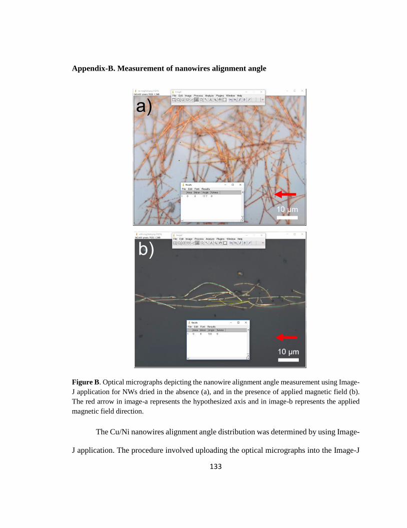
133
Appendix-B. Measurement of nanowires alignment angle
Figure B. Optical micrographs depicting the nanowire alignment angle measurement using Image-
J application for NWs dried in the absence (a), and in the presence of applied magnetic field (b).
The red arrow in image-a represents the hypothesized axis and in image-b represents the applied
magnetic field direction.
The Cu/Ni nanowires alignment angle distribution was determined by using Image-
J application. The procedure involved uploading the optical micrographs into the Image-J

134
application. The measurement angular distribution was performed with respect to a
randomly chosen orientation (in the absence of magnetic field) or applied magnetic field
direction. These studies utilized images such as shown in Figure B. Several (>250 NWs)
isolated nanowires, with two visible ends, were analyzed for NWs alignment angle
distribution and average alignment angles.
Appendix-C. Issues of using ultra-long (>30 µm) nanowires
As the length of the Cu/Ni nanowires increases, the flexibility also increases. Especially,
the magnetic interactions enhance the bending nature of nanowires resulting in
permanently bent nanowire arrangements, see Figure C. The interconnect fabrication
requires the nanowires to be deposited as the straight conductive channels. Therefore, for
the current study, nanowires with the length of less than 30 µm were used.
Figure C. Optical micrograph highlighting the flexibility of ultra-long nanowire (shown in the
yellow box).