Semiconductor Nanowires for Energy...
28
Semiconductor Nanowires for Energy Conversion Allon I. Hochbaum* ,† and Peidong Yang* Department of Chemistry, University of California, Berkeley, California 94720 and Materials Sciences Division, Lawrence Berkeley National Laboratory, Berkeley, California 94720 Received February 26, 2009 Contents 1. Introduction: Role of Materials in Energy Conversion 527 2. Why Are Semiconductor Nanowires Special? 527 3. Electrical and Thermal Transport in Nanowires 528 4. Nanowire Photovoltaic Devices 529 4.1. Conventional Solar Cells 529 4.2. Excitonic Solar Cells 531 4.2.1. Polymer-Inorganic Hybrid Cells 531 4.2.2. Dye-Sensitized Solar Cells 534 5. Nanowires for Electrochemical Energy Storage 536 6. Nanowires for Thermoelectric Applications 539 7. Concluding Remarks 542 8. Acknowledgments 542 9. References 543 1. Introduction: Role of Materials in Energy Conversion Between 2004 and 2030 the annual global consumption of energy is estimated to rise by more than 50%. 1 Assuming current policies and practices remain in place, most of the increased energy production is expected to come from the combustion of fuels, such as oil, ethanol, natural gas, and coal. A commensurate increase in CO 2 (a prominent green- house gas) emissions is anticipated, much of which is due to burning coal—the fastest growing source of energy globally. Despite projected persistent increases in oil and gas prices, less than 10% of the global energy production in 2030 is predicted to come from renewable energy sources, such as hydroelectric, solar, wind, hydrothermal, and biomass. In order to moderate global reliance on exhaustible natural resources and their environmentally hazardous combustion, more scientific efforts should be directed toward reducing the cost of energy production from renewable sources. There exist many potential renewable energy technologies in the form of solid-state devices, such as, for example, solar cells, which convert solar energy in the form of light to the more practical form of electricity. In addition, a large collection of condensed matter phenomena involve the conversion of energy from one form to another, and some proceed with efficiency near unity. Consequently, the study of energy conversion in materials is a field full of opportuni- ties for practical and socially significant applications. Within the last couple of decades there has been increasing interest in materials with nanometer-scale dimensions. Semiconductor nanowires, a subset of these materials, have received exceptional attention for their unique properties and complex structures. Many nanowire-based materials are promising candidates for energy conversion devices. Since electricity is ubiquitously used to power machines and instruments which do work for humans, the practical end product of many energy conversion processes is electrical energy. Even in devices which produce other forms of energy, such as chemical fuel, the conversion process often requires, at least as an intermediate energy state, an electrical potential. For nanowire materials, a fundamental understand- ing of transport in quasi-one-dimensional structures will be crucial to the development of new energy conversion technologies. Moreover, as global power consumption in- creases, there will be an increasing need for new energy storage schemes. Pushing electrons across power grids may not be the ideal solution for many alternative energy technologies. Rather, electrical energy storage in batteries and chemical fuels seems to be a fruitful research direction. To this end, a fundamental understanding of the electro- chemical properties and electron transfer characteristics of nanostructured electrodes and catalysts will be essential. The following sections will review ways in which semiconductor nanowires can enable advanced solid-state energy conversion and storage devices. The discussion of nanowire-based devices will focus on photovoltaic, thermoelectric, and chemical energy storage materials, namely, the conversion of light energy, heat energy, and the energy stored in chemical bonds to electrical potentials and vice versa. 2. Why Are Semiconductor Nanowires Special? The term ‘nanowire’ is generally used to describe a large aspect ratio rod 1-100 nm in diameter (Figure 1). Both descriptors are pertinent to the physical and technological significance of nanowires. First, the diameter puts the radial dimension of these structures at or below the characteristic length scale of various interesting and fundamental solid- state phenomena: the exciton Bohr radius, wavelength of light, phonon mean free path, critical size of magnetic domains, exciton diffusion length, and others. 2,3 As a result, many physical properties of semiconductors are significantly altered within the confines of the nanowire surfaces. In addition, their large surface-to-volume ratio allows for distinct structural and chemical behavior as well as greater chemical reactivity. This two-dimensional confinement en- dows nanowires with unique properties which stray from those of their corresponding bulk material. Second, the large aspect ratio of nanowires intimates their technological application. The one unconstrained dimension can direct the * To whom correspondence should be addressed. E-mail: hochbaum@ seas.harvard.edu (A.H.), [email protected] (P.Y.). † Current address: School of Engineering and Applied Sciences and Department of Chemistry and Chemical Biology, Harvard University, Cambridge, MA 02138. Chem. Rev. 2010, 110, 527–546 527 10.1021/cr900075v 2010 American Chemical Society Published on Web 10/09/2009
Transcript of Semiconductor Nanowires for Energy...
Semiconductor Nanowires for Energy Conversion
Allon I. Hochbaum*,† and Peidong Yang*
Department of Chemistry, University of California, Berkeley, California 94720 and Materials Sciences Division, Lawrence Berkeley NationalLaboratory, Berkeley, California 94720
Received February 26, 2009
Contents
1. Introduction: Role of Materials in EnergyConversion
527
2. Why Are Semiconductor Nanowires Special? 5273. Electrical and Thermal Transport in Nanowires 5284. Nanowire Photovoltaic Devices 529
4.1. Conventional Solar Cells 5294.2. Excitonic Solar Cells 531
4.2.1. Polymer-Inorganic Hybrid Cells 5314.2.2. Dye-Sensitized Solar Cells 534
5. Nanowires for Electrochemical Energy Storage 5366. Nanowires for Thermoelectric Applications 5397. Concluding Remarks 5428. Acknowledgments 5429. References 543
1. Introduction: Role of Materials in EnergyConversion
Between 2004 and 2030 the annual global consumptionof energy is estimated to rise by more than 50%.1 Assumingcurrent policies and practices remain in place, most of theincreased energy production is expected to come from thecombustion of fuels, such as oil, ethanol, natural gas, andcoal. A commensurate increase in CO2 (a prominent green-house gas) emissions is anticipated, much of which is dueto burning coal—the fastest growing source of energyglobally. Despite projected persistent increases in oil and gasprices, less than 10% of the global energy production in 2030is predicted to come from renewable energy sources, suchas hydroelectric, solar, wind, hydrothermal, and biomass. Inorder to moderate global reliance on exhaustible naturalresources and their environmentally hazardous combustion,more scientific efforts should be directed toward reducingthe cost of energy production from renewable sources.
There exist many potential renewable energy technologiesin the form of solid-state devices, such as, for example, solarcells, which convert solar energy in the form of light tothe more practical form of electricity. In addition, a largecollection of condensed matter phenomena involve theconversion of energy from one form to another, and someproceed with efficiency near unity. Consequently, the studyof energy conversion in materials is a field full of opportuni-ties for practical and socially significant applications. Withinthe last couple of decades there has been increasing interest
in materials with nanometer-scale dimensions. Semiconductornanowires, a subset of these materials, have receivedexceptional attention for their unique properties and complexstructures. Many nanowire-based materials are promisingcandidates for energy conversion devices.
Since electricity is ubiquitously used to power machinesand instruments which do work for humans, the practicalend product of many energy conversion processes is electricalenergy. Even in devices which produce other forms ofenergy, such as chemical fuel, the conversion process oftenrequires, at least as an intermediate energy state, an electricalpotential. For nanowire materials, a fundamental understand-ing of transport in quasi-one-dimensional structures will becrucial to the development of new energy conversiontechnologies. Moreover, as global power consumption in-creases, there will be an increasing need for new energystorage schemes. Pushing electrons across power grids maynot be the ideal solution for many alternative energytechnologies. Rather, electrical energy storage in batteriesand chemical fuels seems to be a fruitful research direction.To this end, a fundamental understanding of the electro-chemical properties and electron transfer characteristics ofnanostructured electrodes and catalysts will be essential. Thefollowing sections will review ways in which semiconductornanowires can enable advanced solid-state energy conversionand storage devices. The discussion of nanowire-baseddevices will focus on photovoltaic, thermoelectric, andchemical energy storage materials, namely, the conversionof light energy, heat energy, and the energy stored inchemical bonds to electrical potentials and vice versa.
2. Why Are Semiconductor Nanowires Special?The term ‘nanowire’ is generally used to describe a large
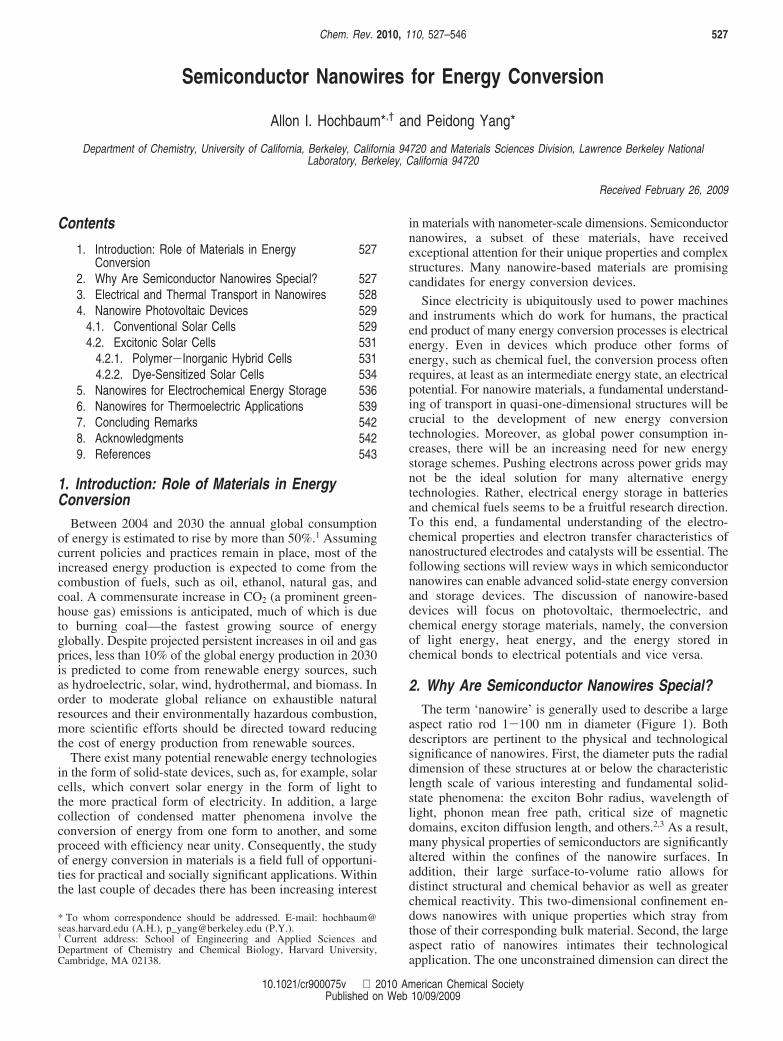
aspect ratio rod 1-100 nm in diameter (Figure 1). Bothdescriptors are pertinent to the physical and technologicalsignificance of nanowires. First, the diameter puts the radialdimension of these structures at or below the characteristiclength scale of various interesting and fundamental solid-state phenomena: the exciton Bohr radius, wavelength oflight, phonon mean free path, critical size of magneticdomains, exciton diffusion length, and others.2,3 As a result,many physical properties of semiconductors are significantlyaltered within the confines of the nanowire surfaces. Inaddition, their large surface-to-volume ratio allows fordistinct structural and chemical behavior as well as greaterchemical reactivity. This two-dimensional confinement en-dows nanowires with unique properties which stray fromthose of their corresponding bulk material. Second, the largeaspect ratio of nanowires intimates their technologicalapplication. The one unconstrained dimension can direct the
* To whom correspondence should be addressed. E-mail: [email protected] (A.H.), [email protected] (P.Y.).† Current address: School of Engineering and Applied Sciences andDepartment of Chemistry and Chemical Biology, Harvard University,Cambridge, MA 02138.
Chem. Rev. 2010, 110, 527–546 527
10.1021/cr900075v 2010 American Chemical SocietyPublished on Web 10/09/2009
conduction of quantum particles such as electrons, phonons,and photons. This control over various forms of energytransport recommends nanowires as ideal materials fromwhich to manufacture advanced solid-state devices. More-over, nanowire lengths are normally sufficient to interfacewith top-down fabrication processes, such as photolithog-raphy. As a result, nanowires provide a convenient platformthrough which researchers may study confined transportphenomena.
3. Electrical and Thermal Transport in NanowiresFor the past decade, exquisite synthetic control has enabled
researchers to specifically tailor nanowire structures andobserve a wide range of electron transport phenomena. Byfine tuning high-quality heterostructures and interfaces withinnanowires, researchers have been able to track single-electrontransport. With small nanowire diameters, the volumeoccupied by conduction electrons is significantly condensed.When the longitudinal dimension is also constrained, in thiscase by the electronic band offset between axial heterojunc-tions, these electrons interact more strongly and repel eachother. In such cases, discrete amounts of energy are requiredto push electrons into these confined volumes and individualelectrons can be manipulated by applied voltages.4 Electrontransport phenomena such as Coulomb blockades5,6 andresonant tunneling7 have been observed in such systems.These properties are useful for fabricating advanced solid-state devices such as resonant tunneling diodes7 and single-electron transistors.8 Additionally, coaxial heterostructurescan be fabricated controllably to produce a one-dimensionalhole gas, which is useful for high-performance field-effect
Allon Hochbaum received his S.B. degree in Materials Science andEngineering from the Massachusetts Institute of Technology in 2003. Hejoined Professor Peidong Yang’s lab and received his Ph.D. degree fromthe Department of Chemistry at U.C. Berkeley in 2008, partly funded byan NSF IGERT fellowship in Nanoscience and Nanotechnology. He iscurrently a postdoctoral research fellow at Harvard University, investigatingbiological and materials interfaces. His research interests include the designand synthesis of nanometer-scale materials with unique properties forenergy conversion and biological applications.
Peidong Yang received his B.S. degree in Chemistry from the Universityof Science and Technology of China in 1993 and Ph.D. degree inChemistry from Harvard University in 1997. He did postdoctoral researchat the University of California, Santa Barbara, before joining the faculty inthe Department of Chemistry at the University of California, Berkeley, in1999. He is currently Professor in the Department of Chemistry, MaterialsScience and Engineering, and a senior faculty scientist at the LawrenceBerkeley National Laboratory. He is the deputy director for the Center ofIntegrated Nanomechanical Systems. He is an associate editor for theJournal of the American Chemical Society and also serves on the EditorialAdvisory Board for a number of journals including Accounts in ChemicalResearch and Nano Letters. He was the first chairperson for the newlyestablished Nanoscience subdivision within the American Chemical Society.He is the recipient of the Alfred P. Sloan research fellowship, Arnold andMabel Beckman Young Investigator Award, National Science FoundationYoung Investigator Award, MRS Young Investigator Award, Julius SpringerPrize for Applied Physics, ACS Pure Chemistry Award, and Alan T.Waterman Award. His main research interest is in the area of one-dimensional semiconductor nanostructures and their applications innanophotonics, nanoelectronics, energy conversion, and nanofluidics.
Figure 1. Scanning electron microscopy images of Si, ZnO, andInGaN nanowires, important semiconductor materials for energyconversion and storage.
528 Chemical Reviews, 2010, Vol. 110, No. 1 Hochbaum and Yang
transistors.9 Nanowires have also been shown to supportcorrelated electron transport, such as superconductivity.10
Synthetic techniques have been developed to the point whereelectronic confinement and unique properties are readilyachieved, and ongoing research is in finding new ways touse and integrate these nanowires into functional devices.
Interesting size-dependent behavior has also been observedfor thermal transport in nanowires. Li and co-workers11,12
discovered that the thermal conductivity of vapor-liquid-solid(VLS) grown Si nanowires is strongly diameter dependent.They found that the thermal conductivity of small diameternanowires is up to 10-fold lower than the bulk value.Furthermore, the temperature dependence of the thermalconductivity at low temperature is highly anomalous for thinwires. Whereas the thermal conductivity is expected to scaleas ∼T3, following the low-temperature heat capacity, it scalesas ∼T2 or even linearly with temperature for the smallestdiameter nanowires. Though this phonon transport is not aswell understood as nanoscale electronic phenomena, theseresults suggest that heat conduction in confined systems is arelatively unexplored and intriguing field of study. It is theseunique charge and thermal transport phenomena that makesemiconductor nanowires promising as building blocks formany of the energy conversion and storage devices reviewedin this manuscript. Not all energy conversion schemes areput to use, many as a result of prohibitive costs. Conse-quently, the goal of much of the following work is two-fold: (1) to study fundamental energy conversion processesin high-quality, well-characterized nanowire systems and (2)to exploit the size dependence of nanowire transport proper-ties to fashion efficient devices using inexpensive andscalable materials and syntheses.
4. Nanowire Photovoltaic Devices
4.1. Conventional Solar CellsAlthough most commercial solar cells are fabricated from
silicon, it has a relatively low absorption coefficient through-out much of the visible and near-infrared parts of theelectromagnetic spectrum.13,14 Because the vast majority ofthe light from the sun is in this range, silicon-based solarcells must be thick in order to collect most of the incidentphotons. For example, a silicon cell must be severalmicrometers to millimeters thick to absorb 90% of theincident light at wavelengths from 700 to 1100 nm, respec-tively, which comprise about one-half of the solar energyavailable above the band gap of silicon.13,15 Conventionalsolar cells are constructed from planar junctions of p- and
n-type semiconductors, where the electrostatic potential atthe interface provides the driving force for charge separation.The collection efficiency of charge carriers generated at agiven distance from the junction, though, depends on theminority carrier diffusion length in the n- and p-type quasi-neutral regions. The minority carrier diffusion length islimited by various recombination mechanisms within thesilicon lattice and their associated relaxation times. Tominimize carrier recombination and thus optimize collectionefficiency, cells must be constructed of high-purity single-crystalline silicon with a large minority carrier diffusionlength. Though highly efficient cells have been fabricatedin the laboratory, practical application of such devices islimited due to the cost of producing and refining such purematerial and the associated device fabrication.
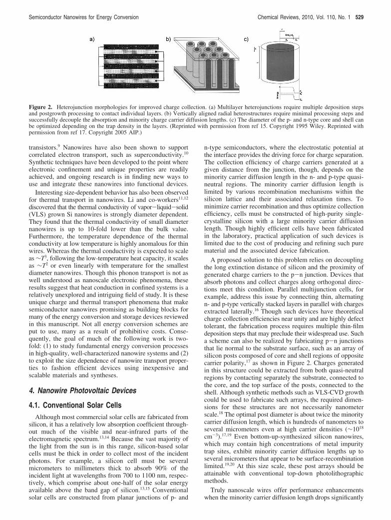
A proposed solution to this problem relies on decouplingthe long extinction distance of silicon and the proximity ofgenerated charge carriers to the p-n junction. Devices thatabsorb photons and collect charges along orthogonal direc-tions meet this condition. Parallel multijunction cells, forexample, address this issue by connecting thin, alternatingn- and p-type vertically stacked layers in parallel with chargesextracted laterally.16 Though such devices have theoreticalcharge collection efficiencies near unity and are highly defecttolerant, the fabrication process requires multiple thin-filmdeposition steps that may preclude their widespread use. Sucha scheme can also be realized by fabricating p-n junctionsthat lie normal to the substrate surface, such as an array ofsilicon posts composed of core and shell regions of oppositecarrier polarity,17 as shown in Figure 2. Charges generatedin this structure could be extracted from both quasi-neutralregions by contacting separately the substrate, connected tothe core, and the top surface of the posts, connected to theshell. Although synthetic methods such as VLS-CVD growthcould be used to fabricate such arrays, the required dimen-sions for these structures are not necessarily nanometerscale.18 The optimal post diameter is about twice the minoritycarrier diffusion length, which is hundreds of nanometers toseveral micrometers even at high carrier densities (∼1018
cm-3).17,19 Even bottom-up-synthesized silicon nanowires,which may contain high concentrations of metal impuritytrap sites, exhibit minority carrier diffusion lengths up toseveral micrometers that appear to be surface-recombinationlimited.19,20 At this size scale, these post arrays should beattainable with conventional top-down photolithographicmethods.
Truly nanoscale wires offer performance enhancementswhen the minority carrier diffusion length drops significantly
Figure 2. Heterojunction morphologies for improved charge collection. (a) Multilayer heterojunctions require multiple deposition stepsand postgrowth processing to contact individual layers. (b) Vertically aligned radial heterostructures require minimal processing steps andsuccessfully decouple the absorption and minority charge carrier diffusion lengths. (c) The diameter of the p- and n-type core and shell canbe optimized depending on the trap density in the layers. (Reprinted with permission from ref 15. Copyright 1995 Wiley. Reprinted withpermission from ref 17. Copyright 2005 AIP.)
Semiconductor Nanowires for Energy Conversion Chemical Reviews, 2010, Vol. 110, No. 1 529

as is the case with highly defective silicon. For manyapplications the critical parameter of power generation is costper Watt. Even relatively inefficient solar cells, therefore,are practical as long as their fabrication costs are low enough.The cost of silicon and substrate processing comprises10-50% of the total cost of a solar cell,14,21,22 and much ofthe cost is due to the purification process, as metallurgicalgrade silicon (99-99.99% purity, or about 1019-1021 impuri-ties per cm3) is 50 times less expensive than higher gradesilicon.23 Consequently, the price per Watt of power fromconventional solar cells could drop significantly if thesedevices tolerated higher defect concentrations.24 The powerconversion efficiency of a solar cell is given as η )(FF|JSC|VOC)/Pin, where FF is the fill factor, JSC is the currentdensity at short circuit (V ) 0), VOC is the photovoltage atopen circuit (I ) 0), and Pin is the incident light powerdensity. The main cause of efficiency losses from latticedefects in silicon solar cells is an increase in the recombina-tion current resulting from minority carrier recombinationat trap sites. Recombination currents can account for a 25%or more decrease in overall cell efficiency, depending onthe energy of the impurity acceptor or donor states, due tolower VOC and FF.25,26 This recombination current varies asIrec ∝ (LnLp)-1, where Ln/p is the minority carrier diffusionlength for n- or p-type carriers and Ln/p ∝ Nt
-1/2, where Nt isthe carrier trap density.26,27 Photovoltaic devices made fromnanostructured dirty silicon would benefit from shorterminority carrier conduction lengths that might mitigate thisproblem.
Several studies of silicon nanowire-based solar cellsprimarily explore the advantages of greater light absorptionwithin the nanowire array. The vertical array geometryscatters light efficiently, especially at short wavelengths, and,depending on the nanowire dimensions, can absorb morelight than a comparably thick solid crystalline film.28 Thisresult has been born out in several studies where the p-njunction lies below the surface of the wafer upon which thearray stands.29-31 Since nanowires do not span the junctionin these devices, the cells behave like conventional single-crystalline p-n junction cells, only with greater absorptionof incident light. These cells, schematically shown in Figure3a, do not reach the efficiencies of conventional cells for acouple reasons. First, the junctions made in the lab bydiffusion doping are generally of poor quality, so the VOC
suffers significantly.29,31 Second, charge extraction occurs
through the nanowires, decreasing JSC due to the larger seriesresistance of the nanowires and their contacts. The lattereffect isespeciallypronouncedin theVLS-grownnanowires30,32
because they cover very little of the substrate surface, thusreducing the conduction cross-section. Consequently, theirefficiencies are 0.1% or less. Mg-doped GaN nanowiresgrown on silicon substrates have analogous antireflectionproperties and power conversion efficiencies of nearly 3%.33
These cells also possess larger internal fields, improving VOC
to 0.95 V. This work is also promising for fabricatingphotovoltaic devices with lattice-mismatched materials sincenanowires can withstand more strain than corresponding thinfilms.34-36
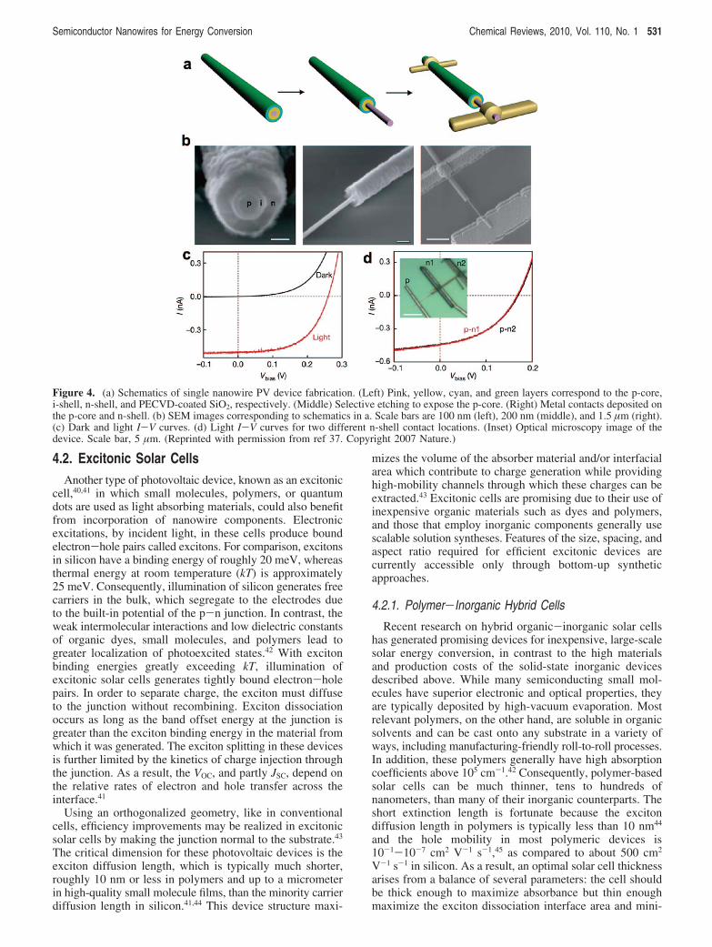
Silicon nanowire radial heterostructures, on the other hand,are the optimal design for efficient charge collection. Thesestructures have been realized with VLS-grown32,37 andelectrolessly etched silicon nanowire arrays.38 Both methodsfirst synthesize the nanowires and then deposit conformalpolycrystalline thin films of intrinsic or complementarypolarity silicon. Garnett and co-workers fabricated radial p-njunctions, shown in Figure 3b and c, on nanowire arrayssynthesized by a scalable, aqueous solution etching synthe-sis39 which exhibit cell efficiencies of about 0.5%. The lowefficiency is due partly to interfacial recombination losses(decreasing VOC and FF), as evidenced by a significant darkcurrent, and partly to a large series resistance in thepolycrystalline shell (decreasing JSC).38 Tian and co-workerssynthesized similar nanowires with p-n and p-i-n radialheterostructures by the VLS mechanism and subsequent thinfilm deposition and characterized the photovoltaic responseof individual nanowires (Figure 4). Though VOC and JSC werenot reported for the p-n device, it is clear from the idealityfactor and breakdown voltage that the p-i-n heterostructurecontains a more robust junction. The VOC of this device issimilar to the radial p-n nanowire arrays of Garnett et al.,but JSC is four to five times greater, possibly a result ofsignificantly lower polycrystalline shell resistivity. The deviceefficiency was calculated to be between 2.3% and 3.4%.Additionally, Tian and co-workers demonstrated a single-nanowire photovoltaic device by selective chemical etchingand contacting the p- and n-type regions separately. More-over, this device was able to power a logic circuit and ananowire pH sensor on a self-contained circuit.37
Figure 3. Nanowire array solar cells. (a) Schematic of a subsurface p-n junction device fabrication process. (b) Schematic of a radialheterostructure nanowire array, and TEM image of one of the synthesized nanowires showing the n-type crystalline core and p-typepolycrystalline shell. (Reprinted with permission from ref 29. Copyright 2005 Wiley. Reprinted with permission from ref 38. Copyright2008 American Chemical Society.)
530 Chemical Reviews, 2010, Vol. 110, No. 1 Hochbaum and Yang
4.2. Excitonic Solar CellsAnother type of photovoltaic device, known as an excitonic
cell,40,41 in which small molecules, polymers, or quantumdots are used as light absorbing materials, could also benefitfrom incorporation of nanowire components. Electronicexcitations, by incident light, in these cells produce boundelectron-hole pairs called excitons. For comparison, excitonsin silicon have a binding energy of roughly 20 meV, whereasthermal energy at room temperature (kT) is approximately25 meV. Consequently, illumination of silicon generates freecarriers in the bulk, which segregate to the electrodes dueto the built-in potential of the p-n junction. In contrast, theweak intermolecular interactions and low dielectric constantsof organic dyes, small molecules, and polymers lead togreater localization of photoexcited states.42 With excitonbinding energies greatly exceeding kT, illumination ofexcitonic solar cells generates tightly bound electron-holepairs. In order to separate charge, the exciton must diffuseto the junction without recombining. Exciton dissociationoccurs as long as the band offset energy at the junction isgreater than the exciton binding energy in the material fromwhich it was generated. The exciton splitting in these devicesis further limited by the kinetics of charge injection throughthe junction. As a result, the VOC, and partly JSC, depend onthe relative rates of electron and hole transfer across theinterface.41
Using an orthogonalized geometry, like in conventionalcells, efficiency improvements may be realized in excitonicsolar cells by making the junction normal to the substrate.43
The critical dimension for these photovoltaic devices is theexciton diffusion length, which is typically much shorter,roughly 10 nm or less in polymers and up to a micrometerin high-quality small molecule films, than the minority carrierdiffusion length in silicon.41,44 This device structure maxi-
mizes the volume of the absorber material and/or interfacialarea which contribute to charge generation while providinghigh-mobility channels through which these charges can beextracted.43 Excitonic cells are promising due to their use ofinexpensive organic materials such as dyes and polymers,and those that employ inorganic components generally usescalable solution syntheses. Features of the size, spacing, andaspect ratio required for efficient excitonic devices arecurrently accessible only through bottom-up syntheticapproaches.
4.2.1. Polymer-Inorganic Hybrid Cells
Recent research on hybrid organic-inorganic solar cellshas generated promising devices for inexpensive, large-scalesolar energy conversion, in contrast to the high materialsand production costs of the solid-state inorganic devicesdescribed above. While many semiconducting small mol-ecules have superior electronic and optical properties, theyare typically deposited by high-vacuum evaporation. Mostrelevant polymers, on the other hand, are soluble in organicsolvents and can be cast onto any substrate in a variety ofways, including manufacturing-friendly roll-to-roll processes.In addition, these polymers generally have high absorptioncoefficients above 105 cm-1.42 Consequently, polymer-basedsolar cells can be much thinner, tens to hundreds ofnanometers, than many of their inorganic counterparts. Theshort extinction length is fortunate because the excitondiffusion length in polymers is typically less than 10 nm44
and the hole mobility in most polymeric devices is10-1-10-7 cm2 V-1 s-1,45 as compared to about 500 cm2
V-1 s-1 in silicon. As a result, an optimal solar cell thicknessarises from a balance of several parameters: the cell shouldbe thick enough to maximize absorbance but thin enoughmaximize the exciton dissociation interface area and mini-
Figure 4. (a) Schematics of single nanowire PV device fabrication. (Left) Pink, yellow, cyan, and green layers correspond to the p-core,i-shell, n-shell, and PECVD-coated SiO2, respectively. (Middle) Selective etching to expose the p-core. (Right) Metal contacts deposited onthe p-core and n-shell. (b) SEM images corresponding to schematics in a. Scale bars are 100 nm (left), 200 nm (middle), and 1.5 µm (right).(c) Dark and light I-V curves. (d) Light I-V curves for two different n-shell contact locations. (Inset) Optical microscopy image of thedevice. Scale bar, 5 µm. (Reprinted with permission from ref 37. Copyright 2007 Nature.)
Semiconductor Nanowires for Energy Conversion Chemical Reviews, 2010, Vol. 110, No. 1 531
mize the series resistance of the cell. Devices similar toconventional parallel multijunction cells have been producedto decouple these design parameters from film thickness.46,47
The poor exciton and charge transport in polymer photo-voltaic devices, though, suggests nanowire array anodes arethe ideal structures to maximize their efficiency.43,45
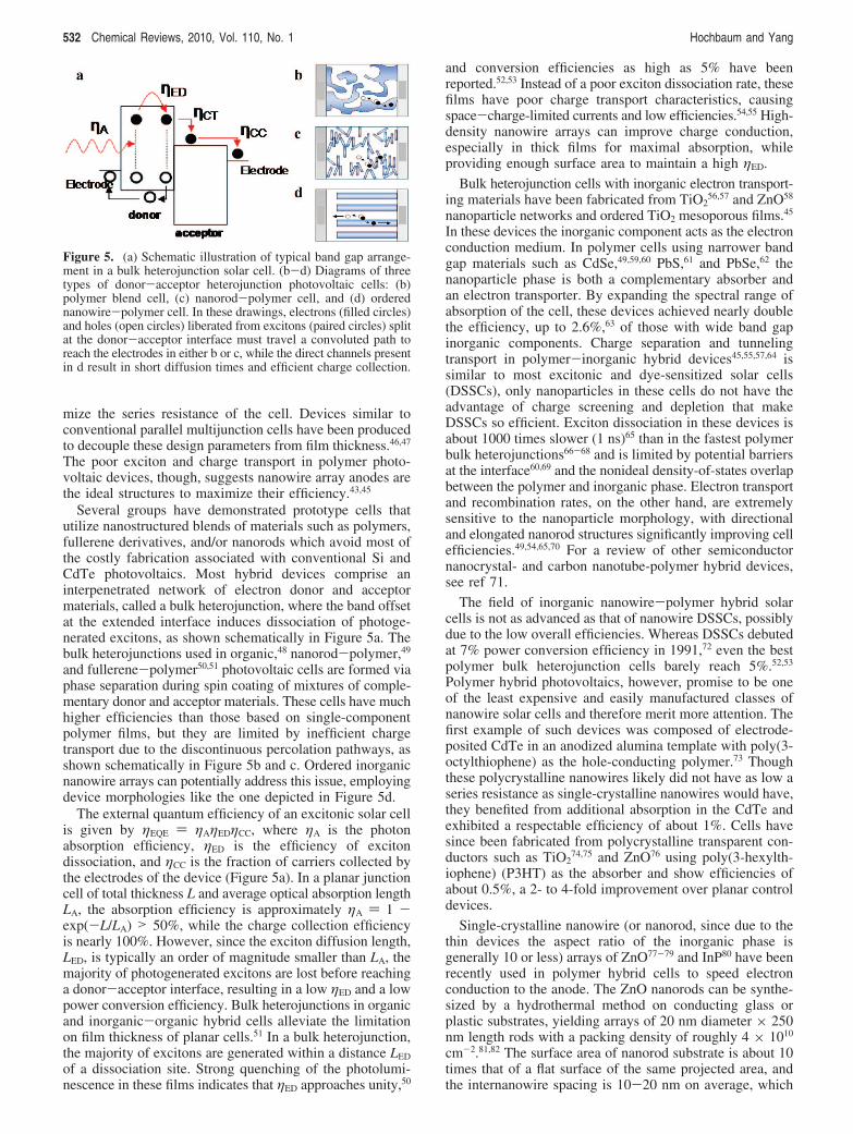
Several groups have demonstrated prototype cells thatutilize nanostructured blends of materials such as polymers,fullerene derivatives, and/or nanorods which avoid most ofthe costly fabrication associated with conventional Si andCdTe photovoltaics. Most hybrid devices comprise aninterpenetrated network of electron donor and acceptormaterials, called a bulk heterojunction, where the band offsetat the extended interface induces dissociation of photoge-nerated excitons, as shown schematically in Figure 5a. Thebulk heterojunctions used in organic,48 nanorod-polymer,49
and fullerene-polymer50,51 photovoltaic cells are formed viaphase separation during spin coating of mixtures of comple-mentary donor and acceptor materials. These cells have muchhigher efficiencies than those based on single-componentpolymer films, but they are limited by inefficient chargetransport due to the discontinuous percolation pathways, asshown schematically in Figure 5b and c. Ordered inorganicnanowire arrays can potentially address this issue, employingdevice morphologies like the one depicted in Figure 5d.
The external quantum efficiency of an excitonic solar cellis given by ηEQE ) ηAηEDηCC, where ηA is the photonabsorption efficiency, ηED is the efficiency of excitondissociation, and ηCC is the fraction of carriers collected bythe electrodes of the device (Figure 5a). In a planar junctioncell of total thickness L and average optical absorption lengthLA, the absorption efficiency is approximately ηA ) 1 -exp(-L/LA) > 50%, while the charge collection efficiencyis nearly 100%. However, since the exciton diffusion length,LED, is typically an order of magnitude smaller than LA, themajority of photogenerated excitons are lost before reachinga donor-acceptor interface, resulting in a low ηED and a lowpower conversion efficiency. Bulk heterojunctions in organicand inorganic-organic hybrid cells alleviate the limitationon film thickness of planar cells.51 In a bulk heterojunction,the majority of excitons are generated within a distance LED
of a dissociation site. Strong quenching of the photolumi-nescence in these films indicates that ηED approaches unity,50
and conversion efficiencies as high as 5% have beenreported.52,53 Instead of a poor exciton dissociation rate, thesefilms have poor charge transport characteristics, causingspace-charge-limited currents and low efficiencies.54,55 High-density nanowire arrays can improve charge conduction,especially in thick films for maximal absorption, whileproviding enough surface area to maintain a high ηED.
Bulk heterojunction cells with inorganic electron transport-ing materials have been fabricated from TiO2
56,57 and ZnO58
nanoparticle networks and ordered TiO2 mesoporous films.45
In these devices the inorganic component acts as the electronconduction medium. In polymer cells using narrower bandgap materials such as CdSe,49,59,60 PbS,61 and PbSe,62 thenanoparticle phase is both a complementary absorber andan electron transporter. By expanding the spectral range ofabsorption of the cell, these devices achieved nearly doublethe efficiency, up to 2.6%,63 of those with wide band gapinorganic components. Charge separation and tunnelingtransport in polymer-inorganic hybrid devices45,55,57,64 issimilar to most excitonic and dye-sensitized solar cells(DSSCs), only nanoparticles in these cells do not have theadvantage of charge screening and depletion that makeDSSCs so efficient. Exciton dissociation in these devices isabout 1000 times slower (1 ns)65 than in the fastest polymerbulk heterojunctions66-68 and is limited by potential barriersat the interface60,69 and the nonideal density-of-states overlapbetween the polymer and inorganic phase. Electron transportand recombination rates, on the other hand, are extremelysensitive to the nanoparticle morphology, with directionaland elongated nanorod structures significantly improving cellefficiencies.49,54,65,70 For a review of other semiconductornanocrystal- and carbon nanotube-polymer hybrid devices,see ref 71.
The field of inorganic nanowire-polymer hybrid solarcells is not as advanced as that of nanowire DSSCs, possiblydue to the low overall efficiencies. Whereas DSSCs debutedat 7% power conversion efficiency in 1991,72 even the bestpolymer bulk heterojunction cells barely reach 5%.52,53
Polymer hybrid photovoltaics, however, promise to be oneof the least expensive and easily manufactured classes ofnanowire solar cells and therefore merit more attention. Thefirst example of such devices was composed of electrode-posited CdTe in an anodized alumina template with poly(3-octylthiophene) as the hole-conducting polymer.73 Thoughthese polycrystalline nanowires likely did not have as low aseries resistance as single-crystalline nanowires would have,they benefited from additional absorption in the CdTe andexhibited a respectable efficiency of about 1%. Cells havesince been fabricated from polycrystalline transparent con-ductors such as TiO2
74,75 and ZnO76 using poly(3-hexylth-iophene) (P3HT) as the absorber and show efficiencies ofabout 0.5%, a 2- to 4-fold improvement over planar controldevices.
Single-crystalline nanowire (or nanorod, since due to thethin devices the aspect ratio of the inorganic phase isgenerally 10 or less) arrays of ZnO77-79 and InP80 have beenrecently used in polymer hybrid cells to speed electronconduction to the anode. The ZnO nanorods can be synthe-sized by a hydrothermal method on conducting glass orplastic substrates, yielding arrays of 20 nm diameter × 250nm length rods with a packing density of roughly 4 × 10¹⁰
cm-2.81,82 The surface area of nanorod substrate is about 10times that of a flat surface of the same projected area, andthe internanowire spacing is 10-20 nm on average, which
Figure 5. (a) Schematic illustration of typical band gap arrange-ment in a bulk heterojunction solar cell. (b-d) Diagrams of threetypes of donor-acceptor heterojunction photovoltaic cells: (b)polymer blend cell, (c) nanorod-polymer cell, and (d) orderednanowire-polymer cell. In these drawings, electrons (filled circles)and holes (open circles) liberated from excitons (paired circles) splitat the donor-acceptor interface must travel a convoluted path toreach the electrodes in either b or c, while the direct channels presentin d result in short diffusion times and efficient charge collection.
532 Chemical Reviews, 2010, Vol. 110, No. 1 Hochbaum and Yang
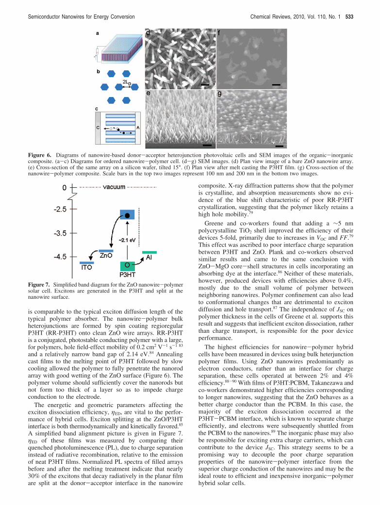
is comparable to the typical exciton diffusion length of thetypical polymer absorber. The nanowire-polymer bulkheterojunctions are formed by spin coating regioregularP3HT (RR-P3HT) onto clean ZnO wire arrays. RR-P3HTis a conjugated, photostable conducting polymer with a large,for polymers, hole field-effect mobility of 0.2 cm2 V-1 s-1 83
and a relatively narrow band gap of 2.14 eV.84 Annealingcast films to the melting point of P3HT followed by slowcooling allowed the polymer to fully penetrate the nanorodarray with good wetting of the ZnO surface (Figure 6). Thepolymer volume should sufficiently cover the nanorods butnot form too thick of a layer so as to impede chargeconduction to the electrode.
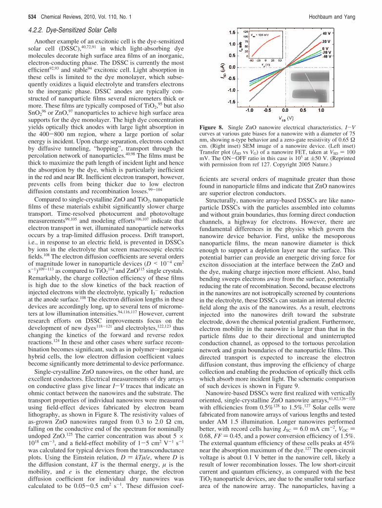
The energetic and geometric parameters affecting theexciton dissociation efficiency, ηED, are vital to the perfor-mance of hybrid cells. Exciton splitting at the ZnO/P3HTinterface is both thermodynamically and kinetically favored.85
A simplified band alignment picture is given in Figure 7.ηED of these films was measured by comparing theirquenched photoluminescence (PL), due to charge separationinstead of radiative recombination, relative to the emissionof neat P3HT films. Normalized PL spectra of filled arraysbefore and after the melting treatment indicate that nearly30% of the excitons that decay radiatively in the planar filmare split at the donor-acceptor interface in the nanowire
composite. X-ray diffraction patterns show that the polymeris crystalline, and absorption measurements show no evi-dence of the blue shift characteristic of poor RR-P3HTcrystallization, suggesting that the polymer likely retains ahigh hole mobility.79
Greene and co-workers found that adding a ∼5 nmpolycrystalline TiO2 shell improved the efficiency of theirdevices 5-fold, primarily due to increases in VOC and FF.79
This effect was ascribed to poor interface charge separationbetween P3HT and ZnO. Plank and co-workers observedsimilar results and came to the same conclusion withZnO-MgO core-shell structures in cells incorporating anabsorbing dye at the interface.86 Neither of these materials,however, produced devices with efficiencies above 0.4%,mostly due to the small volume of polymer betweenneighboring nanowires. Polymer confinement can also leadto conformational changes that are detrimental to excitondiffusion and hole transport.87 The independence of JSC onpolymer thickness in the cells of Greene et al. supports thisresult and suggests that inefficient exciton dissociation, ratherthan charge transport, is responsible for the poor deviceperformance.
The highest efficiencies for nanowire-polymer hybridcells have been measured in devices using bulk heterjunctionpolymer films. Using ZnO nanowires predominantly aselectron conductors, rather than an interface for chargeseparation, these cells operated at between 2% and 4%efficiency.88-90 With films of P3HT:PCBM, Takanezawa andco-workers demonstrated higher efficiencies correspondingto longer nanowires, suggesting that the ZnO behaves as abetter charge conductor than the PCBM. In this case, themajority of the exciton dissociation occurred at theP3HT-PCBM interface, which is known to separate chargeefficiently, and electrons were subsequently shuttled fromthe PCBM to the nanowires.89 The inorganic phase may alsobe responsible for exciting extra charge carriers, which cancontribute to the device JSC. This strategy seems to be apromising way to decouple the poor charge separationproperties of the nanowire-polymer interface from thesuperior charge conduction of the nanowires and may be theideal route to efficient and inexpensive inorganic-polymerhybrid solar cells.
Figure 6. Diagrams of nanowire-based donor-acceptor heterojunction photovoltaic cells and SEM images of the organic-inorganiccomposite. (a-c) Diagrams for ordered nanowire-polymer cell. (d-g) SEM images. (d) Plan view image of a bare ZnO nanowire array.(e) Cross-section of the same array on a silicon wafer, tilted 15°. (f) Plan view after melt casting the P3HT film. (g) Cross-section of thenanowire-polymer composite. Scale bars in the top two images represent 100 nm and 200 nm in the bottom two images.
Figure 7. Simplified band diagram for the ZnO nanowire-polymersolar cell. Excitons are generated in the P3HT and split at thenanowire surface.
Semiconductor Nanowires for Energy Conversion Chemical Reviews, 2010, Vol. 110, No. 1 533
4.2.2. Dye-Sensitized Solar Cells
Another example of an excitonic cell is the dye-sensitizedsolar cell (DSSC),40,72,91 in which light-absorbing dyemolecules decorate high surface area films of an inorganic,electron-conducting phase. The DSSC is currently the mostefficient92,93 and stable94 excitonic cell. Light absorption inthese cells is limited to the dye monolayer, which subse-quently oxidizes a liquid electrolyte and transfers electronsto the inorganic phase. DSSC anodes are typically con-structed of nanoparticle films several micrometers thick ormore. These films are typically composed of TiO2,95 but alsoSnO2
96 or ZnO,97 nanoparticles to achieve high surface areasupports for the dye monolayer. The high dye concentrationyields optically thick anodes with large light absorption inthe 400-800 nm region, where a large portion of solarenergy is incident. Upon charge separation, electrons conductby diffusive tunneling, “hopping”, transport through thepercolation network of nanoparticles.40,98 The films must bethick to maximize the path length of incident light and hencethe absorption by the dye, which is particularly inefficientin the red and near IR. Inefficient electron transport, however,prevents cells from being thicker due to low electrondiffusion constants and recombination losses.99-104
Compared to single-crystalline ZnO and TiO2, nanoparticlefilms of these materials exhibit significantly slower chargetransport. Time-resolved photocurrent and photovoltagemeasurements99,105 and modeling efforts106,107 indicate thatelectron transport in wet, illuminated nanoparticle networksoccurs by a trap-limited diffusion process. Drift transport,i.e., in response to an electric field, is prevented in DSSCsby ions in the electrolyte that screen macroscopic electricfields.108 The electron diffusion coefficients are several ordersof magnitude lower in nanoparticle devices (D < 10-4 cm2
s-1)109-113 as compared to TiO2114 and ZnO115 single crystals.
Remarkably, the charge collection efficiency of these filmsis high due to the slow kinetics of the back reaction ofinjected electrons with the electrolyte, typically I3
- reductionat the anode surface.108 The electron diffusion lengths in thesedevices are accordingly long, up to several tens of microme-ters at low illumination intensities.94,116,117 However, currentresearch efforts on DSSC improvements focus on thedevelopment of new dyes118-121 and electrolytes,122,123 thuschanging the kinetics of the forward and reverse redoxreactions.124 In these and other cases where surface recom-bination becomes significant, such as in polymer-inorganichybrid cells, the low electron diffusion coefficient valuesbecome significantly more detrimental to device performance.
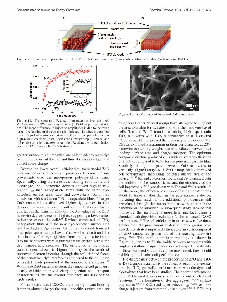
Single-crystalline ZnO nanowires, on the other hand, areexcellent conductors. Electrical measurements of dry arrayson conductive glass give linear I-V traces that indicate anohmic contact between the nanowires and the substrate. Thetransport properties of individual nanowires were measuredusing field-effect devices fabricated by electron beamlithography, as shown in Figure 8. The resistivity values ofas-grown ZnO nanowires ranged from 0.3 to 2.0 Ω cm,falling on the conductive end of the spectrum for nominallyundoped ZnO.125 The carrier concentration was about 5 ×1018 cm-3, and a field-effect mobility of 1-5 cm2 V-1 s-1
was calculated for typical devices from the transconductanceplots. Using the Einstein relation, D ) kTµ/e, where D isthe diffusion constant, kT is the thermal energy, µ is themobility, and e is the elementary charge, the electrondiffusion coefficient for individual dry nanowires wascalculated to be 0.05-0.5 cm2 s-1. These diffusion coef-
ficients are several orders of magnitude greater than thosefound in nanoparticle films and indicate that ZnO nanowiresare superior electron conductors.
Structurally, nanowire array-based DSSCs are like nano-particle DSSCs with the particles assembled into columnsand without grain boundaries, thus forming direct conductionchannels, a highway for electrons. However, there arefundamental differences in the physics which govern thenanowire device behavior. First, unlike the mesoporousnanoparticle films, the mean nanowire diameter is thickenough to support a depletion layer near the surface. Thispotential barrier can provide an energetic driving force forexciton dissociation at the interface between the ZnO andthe dye, making charge injection more efficient. Also, bandbending sweeps electrons away from the surface, potentiallyreducing the rate of recombination. Second, because electronsin the nanowires are not isotropically screened by counterionsin the electrolyte, these DSSCs can sustain an internal electricfield along the axis of the nanowires. As a result, electronsinjected into the nanowires drift toward the substrateelectrode, down the chemical potential gradient. Furthermore,electron mobility in the nanowire is larger than that in theparticle films due to their directional and uninterruptedconduction channel, as opposed to the tortuous percolationnetwork and grain boundaries of the nanoparticle films. Thisdirected transport is expected to increase the electrondiffusion constant, thus improving the efficiency of chargecollection and enabling the production of optically thick cellswhich absorb more incident light. The schematic comparisonof such devices is shown in Figure 9.
Nanowire-based DSSCs were first realized with verticallyoriented, single-crystalline ZnO nanowire arrays,81,82,126-128
with efficiencies from 0.5%128 to 1.5%.127 Solar cells werefabricated from nanowire arrays of various lengths and testedunder AM 1.5 illumination. Longer nanowires performedbetter, with record cells having JSC ) 6.0 mA cm-2, VOC )0.68, FF ) 0.45, and a power conversion efficiency of 1.5%.The external quantum efficiency of these cells peaks at 45%near the absorption maximum of the dye.127 The open-circuitvoltage is about 0.1 V better in the nanowire cell, likely aresult of lower recombination losses. The low short-circuitcurrent and quantum efficiency, as compared with the bestTiO2 nanoparticle devices, are due to the smaller total surfacearea of the nanowire array. The nanoparticles, having a
Figure 8. Single ZnO nanowire electrical characteristics. I-Vcurves at various gate biases for a nanowire with a diameter of 75nm, showing n-type behavior and a zero-gate resistivity of 0.65 Ωcm. (Right inset) SEM image of a nanowire device. (Left inset)Transfer plot (ISD vs VG) of a nanowire FET, taken at VSD ) 100mV. The ON-OFF ratio in this case is 105 at (50 V. (Reprintedwith permission from ref 127. Copyright 2005 Nature.)
534 Chemical Reviews, 2010, Vol. 110, No. 1 Hochbaum and Yang
greater surface to volume ratio, are able to adsorb more dyeper unit thickness of the cell and thus absorb more light andcollect more charge.
Despite the lower overall efficiencies, these model ZnOnanowire devices demonstrate promising fundamental im-provements over the mesoporous polycrystalline films.Specifically, using the same dye, loading conditions, andelectrolyte, ZnO nanowire devices showed significantlyhigher JSC than nanoparticle films with the same dye-adsorbed surface area. Law and co-workers found that,consistent with studies on TiO2 nanoparticle films,129 largerZnO nanoparticles displayed higher JSC values in thindevices, presumably as a result of the higher diffusionconstant in the films. In addition, the JSC values of the ZnOnanowire devices were still higher, suggesting a lower seriesresistance within the cell.130 Devices composed of TiO2
nanoparticle films with the same dye-adsorbed surface areahad the highest JSC values. Using femtosecond transientabsorption spectroscopy, Law and co-workers also found thatthe kinetics of charge injection from the dye excited stateinto the nanowires were significantly faster than across thedye-nanoparticle interface. The difference in the chargetransfer rates, shown in Figure 10, may be the result ofimproved electron injection through the well-defined facetsof the nanowire-dye interface as compared to the multitudeof crystal facets presented at the nanoparticle surfaces.127
Within the ZnO material system, the nanowire cell geometryclearly exhibits improved charge injection and transportcharacteristics, but the overall efficiency still lags behindTiO2 anodes.
For nanowire-based DSSCs, the most significant limitingfactor is almost always the small specific surface area (or
roughness factor). Several groups have attempted to augmentthe area available for dye absorption in the nanowire-basedcells. Tan and Wu131 found that mixing high aspect ratioTiO2 nanowires with TiO2 nanoparticles in a disorderedDSSC anode film improved the efficiency of the device. TheDSSCs exhibited a maximum in their performance, at 20%nanowire content by weight, due to a balance between dyeloading surface area and charge transport. The optimumcomposite mixture produced cells with an average efficiencyof 8.6% as compared to 6.7% for the pure nanoparticle film.Similarly, filling the space between ZnO nanowires invertically aligned arrays with ZnO nanoparticles improvedcell performance, increasing the total surface area of thedevice.132,133 Ku and co-workers found that JSC increased withthe addition of the nanoparticles, and the efficiency of thecell improved 3-fold, consistent with Tan and Wu’s results.132
Furthermore, the effective electron diffusion constant wasabout 10 times smaller than in the pure nanowire device,indicating that much of the additional photocurrent stillpercolated through the nanoparticle network to either thenanowire or the substrate. A subsequent study showed thatimproving the nanowire-nanoparticle interface using achemical bath deposition technique further enhanced DSSCperformance.134 The cell efficiency in this case was five timesgreater than the pure nanowire device. Other groups havealso demonstrated improved efficiencies in cells composedof ZnO nanowires grown off of the existing nanowirearray.135,136 This tree-like anode morphology, as shown inFigure 11, serves to fill the voids between nanowires withsingle-crystalline charge conduction pathways. If the densityof these branched structures can be maximized, they shouldexhibit optimal solar cell performance.
The discrepancy between the properties of ZnO and TiO2
as DSSC anode materials is the subject of ongoing investiga-tion, but TiO2 generally performs better with the dyes andelectrolytes that have been studied. The poorer performanceof the ZnO-based devices may be a result of surface chemicalreactions,137 the formation of dye aggregates,138,139 surfacetrap states,140,141 ZnO seed layer processing,142,143 or slowcharge injection from commonly used dyes.105,144,145 To this
Figure 9. Schematic representations of a DSSC. (a) Traditional cell (nanoparticle film electrode). (b) Nanowire DSSCs.
Figure 10. Transient mid-IR absorption traces of dye-sensitizedZnO nanowire (NW) and nanoparticle (NP) films pumped at 400nm. The large difference in injection amplitudes is due to the muchlarger dye loading of the particle film. Injection in wires is completeafter ∼5 ps but continues out to ∼100 ps in the particle case. Ahigh-resolution trace (inset) shows the ultrafast step (<250 fs) and∼3 ps rise time for a nanowire sample. (Reprinted with permissionfrom ref 127. Copyright 2005 Nature.)
Figure 11. SEM image of branched ZnO nanowires.
Semiconductor Nanowires for Energy Conversion Chemical Reviews, 2010, Vol. 110, No. 1 535
end, several groups have employed radial (core-shell)nanowire heterostructures to exploit the charge transfercharacteristics and surface stability of TiO2 while retainingthe fast electron transport of single-crystalline nanowires.Law and co-workers146 synthesized ZnO nanowire arrayscoated by atomic layer deposition (ALD) with TiO2 filmsof varying thickness. The difference between the Fermi levelsof the ZnO core and TiO2 shell creates a weak type II bandoffset at the interface, which provides a potential barrier tocharge recombination. Overall, the core-shell devicesexhibited a 2-fold improvement in efficiency (0.85-2.1%)that was attributed to a combination of improved chargeinjection and reduced recombination current.147 Similardevices were constructed using SnO2 nanowires as theconducting core with TiO2 nanoparticle148 and ALD-deposited148,149 films. The nanoparticle-coated arrays gavethe best device efficiencies, about 4%, and recombinationtime constants, as calculated from VOC decay curves, wereabout 100-fold longer for the nanowire arrays than thenanoparticle films.
Although ZnO appears to be an inferior material to TiO2
as the DSSC anode, model TiO2 nanowire array structureshave proved a significant synthetic challenge. Varioustechniques have been developed to reduce the resistance toelectron transport between particles, such as growth ofaligned polycrystalline nanotubes,150-152 high-temperaturesintering,153 ordering of the mesoporous structure,154,155 andsynthesis of particle films by oriented attachment.156 All thesemethods strive to minimize electronic defects at the grainboundaries, but none will likely demonstrate as great animprovement as high surface area single crystals. Thedecreased density of trap states leading to faster electrontransport improves overall cell performance only whencoupled with the energetic barrier to charge recombinationprovided by the nanowire structure.100,157 Recently, severalgroups have achieved high-density, single-crystalline, verti-cally aligned TiO2 nanowire arrays.158,159 The efficiency ofDSSCs fabricated from these arrays is encouraging, about5%, though the nanowire density is too low such that thesurface area available for dye adsorption suffers.158 Withfurther synthetic optimization, or perhaps combination withnanoparticles in a composite film, these TiO2 nanowireanodes are promising candidates for high-efficiency DSSCs.
Analogous photovoltaic devices based on the principlesof DSSCs have also been fabricated on ZnO nanowiresubstrates. Leschkies and co-workers used CdSe quantumdots, instead of an absorbing dye, to sensitize arrays of ZnOnanowires immersed in an I2/I3
- redox couple solution.Though the cell efficiency was low (0.4%), it had areasonable VOC of 0.6 V and an internal quantum efficiencyof 50-60% over the wavelengths corresponding to the firstexcitonic transition of the nanoparticles.160 Different nano-particle sizes or compositions can be used to tune theabsorption range of these cells independent of surfacechemistry, unlike the sensitizing dyes. All inorganic-sensitized solar cells were fabricated on a ZnO nanowirearray, with a CdSe or CdTe absorber layer, and CuSCNtransparent hole-conducting layer deposited from a chemicalbath solution.161,162 The cells with the CdSe absorber layerperformed better, with a 2.3% power conversion efficiencyat low illumination intensities (36 mW cm2), but bothsuffered from significant recombination losses.
The energy conversion efficiencies of current nanowire-based excitonic cells are not better than the best nanoparticle-
based DSSCs, but the studies discussed above show that theirelectron transport properties are superior. Nanoparticle filmshave at least a 5-fold larger surface area than the bestnanowire arrays, resulting in more dye loading per area ofthe cell and hence more absorption within the particle films.Longer or thinner nanowire arrays with comparable surfaceareas are a synthetic challenge, but they should improve bothlight absorption and charge transport within the anode.
Inorganic nanowires represent an ideal charge transportmedium for nanostructured solar cells and display promisingimprovements over planar and nanoparticle-based devices.Further efficiency improvements may be realized in severalareas of research. (1) Better synthetic control. Ideal electrodestructures have not been realized, in terms of both theirsurface area and length as well as their band gap. (2)Improved device architectures. The performance of nanorod-polymer devices has been disappointing thus far. Incorporat-ing different absorbers, such as small molecules or nano-crystals, and hole conductors, such as inorganic layers, in avariety of device schemes would provide comparative datato help understand the factors that determine efficiency.Atomic layer deposition is a particularly useful technique inthis regard. (3) Time-dependent transport experiments. Time-and frequency-domain photocurrent and voltage experimentsmay shed light on the charge separation and transportproperties of nanowire-based solar cell. (4) Device modeling.Three-dimensional models of nanostructured solar cellswould help explain the role of electric fields and themicroscopic dynamics of recombination in these cells.
5. Nanowires for Electrochemical Energy StorageThe storage of energy through electrochemical reactions
is a crucial technology for portable power needs and loadleveling of many alternative and conventional power sources.The proliferation of personal electronics and commercializa-tion of electric and hybrid electric vehicles has popularizedthe need for rechargeable, portable power sources. High-capacity energy storage is also necessary for the widespreaduse of intermittent alternative energy resources, most notablyfrom the sun and wind. For these technologies to contributesignificantly to the global demand for electricity, they requireefficient methods to store excess energy when it is abundant,during the day, for example, or when the wind blows, andto release it as needed. Such storage would also improvethe efficiency of conventional power generation by levelingthe peaks and valleys of daily energy demand.163,164 Batteriesfulfill these requirements by providing a direct route to theconversion of electrical to chemical energy.
The basis for this energy conversion is the simultaneousshuttling of electrons to and from electrodes via comple-mentary chemical reactions. During discharge, electrons aredelivered from the cathode to the anode through an electro-lyte medium by spontaneous reduction and oxidation,respectively, of chemical species at the electrodes. Electronssupply power by flowing from the anode back to the cathodethrough an external load. Applying an opposing voltageacross the cell reverses the reactions at the electrodes, thusrecharging the battery capacity. Fuel cells are similar tobatteries in that spontaneous redox reactions at the electrodesproduce a voltage to push electrons across an external load.The reactants for these reactions, however, are generally notrecycled within the cell but rather supplied to the electrodesfrom an external source as liquids or gases. In a hydrogenfuel cell, for example, hydrogen and oxygen gas are oxidized
536 Chemical Reviews, 2010, Vol. 110, No. 1 Hochbaum and Yang
and reduced at the anode and cathode, respectively, formingwater, which is subsequently removed. Similarly, photoelec-trochemical (PEC) cells use a photovoltage, instead of anexternally applied voltage, to drive redox reactions at theelectrode surfaces in a process analogous to battery charging.The DSSC devices discussed above are in fact PEC cellswhere the chemical fuel, the oxidized electrolyte, is convertedback to an electrical potential internally. The factors affectingPEC efficiencies are therefore similar to those in the DSSCsection above and will not be covered in further detail.Suffice it to say that nanowires have been used in PECdevices with some demonstrated advantages over planar andnanoparticle-based electrodes.152,165-174
Lithium ion batteries, which use lithium cations totransport charge between electrodes, are promising forrechargeable chemical energy storage due to the fast mobilityand high energy density of lithium ions. Lithium also has alarge negative reduction potential (E0 ) -3.05 V) whichgenerates a high-voltage output. Only hydrogen would offerbetter storage and transport properties if not for the difficultyof storing large weight fractions of it.163 The energy storedin these batteries is a result of the difference in the redoxpotentials of lithium insertion into the two electrodes. As aresult, the battery capacity depends on the weight or volumefraction of lithium that each electrode can hold, and the rateof charging and discharging depends on the electricalresistance of the electrodes and the rate of lithium diffusionin and out of the electrode materials.164
Nanoparticles have been employed as electrode materialsto improve cell properties in several ways. First, smalldiameter particles have large surface-to-volume ratios andshort lithium diffusion lengths. The diffusion time varies asthe square of the length, so the greater available surface areaand reduction of particle sizes from micro- to nanometersresult in orders of magnitude increases in lithium insertionand discharging kinetics. Nam and co-workers, for example,used viral capsid templates to nucleate monodisperse Co3O4
and Au-Co3O4 composite nanoparticles by a low-temper-ature synthesis, which exhibited superior lithium storage anddischarge properties normally found only in higher temper-ature syntheses (∼500 °C).175 Second, nanoparticles maysustain more damaging structural changes than their bulkmaterial counterparts. Particles below a critical size mayresist phase transformations176 or undergo transitions throughand amorphous intermediate177,178 and prevent large latticestrains resulting from phase coexistence. Furthermore, nano-particles resist cracking due to strain relaxation at thesurface179,180 and mechanical considerations.181 Finally, thehigh surface-to-volume ratio of the nanoparticle electrodesincreases their reactivity significantly, which allows fordifferent reaction mechanisms than are observed at bulkmaterial surfaces. For example, instead of incorporating intothe lattice of several metal-oxide electrode materials, lithiumreversibly reduces the electrodes to metal particles sur-rounded by LixO.182
As with PEC or solar cells, nanoparticle battery electrodessuffer from poor charge transport. While some materials withhigh lithium storage capacities are inherently poor conduc-tors, the cyclic strain fluctuations of the electrodes uponlithium insertion and removal causes greater separationbetween nanoparticles and impedes charge percolation to andfrom the current collectors. The former can be addressedwith impurity doping of the electrode material, though thesedefects may lead to deterioration of the electrochemical
properties of the electrode. The latter problem is oftenremedied by encapsulating the nanoparticles in a conductivecarbon matrix, thus reducing the series resistance to thecurrent collector.176 Carbon, however, even in the form ofgraphite has a limited capacity for intercalating lithium, suchthat a pure graphite electrode can reach a specific capacityof about 350 mAh g-1.164,183 As a result, the specific capacityof the electrode suffers. In materials such as silicon and tinthe effects of volume expansion and contraction (up to 400%for Li4.4Si) are exacerbated due to their especially highcapacity for lithium.184 For a comprehensive review of siliconnanoparticle-based anodes, see ref 185. The high lithiumcontent of these alloys though is precisely the property thatmakes these materials so attractive for battery anodes.
Due to the lack of a conductive matrix, nanometer-scalethin films of amorphous silicon exhibit much greater specificcapacities than nanoparticle electrodes and longer cycle livesthan bulk silicon.185 These films routinely store >3000-4000mAh g-1 due to their large surface-to-volume ratio andexhibit excellent capacity retention up to several hundredcycles. For up to 200 cycles, Ohara and co-workers foundthat thinner amorphous silicon films had a greater specificcapacity, 3700, 2900, and 2900 mAh g-1 for 50, 150, and440 nm films, and that the capacity loss per cycle increasedwith thickness.186,187 Their results follow this trend up tothicker films of several micrometers.188 The researchersconcluded that the improved charge retention in the thinnerfilms was a result of less cracking and degradation of theelectrical contact between the thinner films and theirsubstrates. The thinner the films, the better they were ableto withstand the expansion and contraction cycles underlithium loading. Although these results are fundamentallysignificant, the application of thin films in commercial batterytechnologies seems limited since the surface area accessibleto the electrolyte is limited by the area of the substrate.
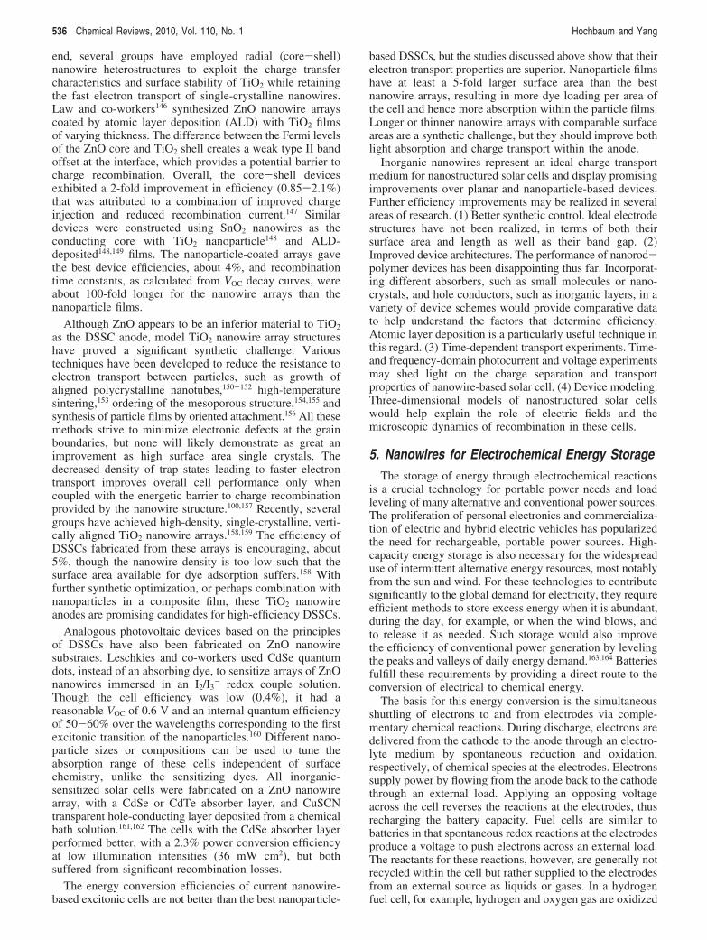
Nanowire anodes, in contrast to nanoparticle and thin filmmaterials, should in principle maximize the electrode surfacearea while maintaining good electrical connections to thecurrent collector (Figure 12). Indeed, Gao and co-workersadopted this strategy for VLS-grown silicon and germaniumnanowires but with disappointing capacities of about800-1500 mAh g-1 and no cycling experiments.189 Chanand co-workers discovered they could achieve near theoreti-cal specific capacity (4200 mAh g-1) for VLS-grown siliconnanowire anodes on a stainless steel current collector.190 Theanode capacity fell immediately following the first cycle butremained constant at about 3000 mAh g-1 for 10 cycles ata C/20 rate (i.e., discharging 1/20th the cell capacity perhour). Another device exhibited a capacity of roughly 3500mAh g-1 for 20 cycles at a C/5 rate. TEM images show thatthe initially single-crystalline nanowires became amorphousafter lithium insertion and reverted to amorphous silicon afterthe first discharge cycle. Ge nanowire anodes synthesizedin a similar manner exhibited analogous results, albeit at alower specific capacity of 1141 mAh g-1 over 20 cycles ata C/20 rate.191 With another variation, Cui and co-workersinvestigatedthecyclingbehaviorofcrystallinecore-amorphousshell silicon nanowire anodes also grown by the VLSmechanism.192 Due to differences in the reduction potentialof lithium in amorphous versus crystalline silicon, theresearchers proposed that the core could serve as a mechan-ical support and provide high electrical conductivity alongthe entire length of the nanowire array. Indeed, the lithiumreduction peaks were distinguishable in electrochemical
Semiconductor Nanowires for Energy Conversion Chemical Reviews, 2010, Vol. 110, No. 1 537
potential spectroscopy scans. Although cycling below thecrystalline silicon reduction potential for lithium produceda large initial specific capacity, 2400 mAh g-1, the capacitydropped about 20% over 30 cycles. By cycling the cells witha lower voltage limit above this potential, the anodesexhibited lower capacities, about 800-1000 mAh g-1, butlost less than 10% of their capacity over 100 cycles, makingthem promising candidates for practical applications.
Other nanowire-based anodes have been studied in avariety of material systems and also demonstrate improvedproperties as compared to nanoparticle and bulk materials.Mesoporous materials, essentially inverse nanowire struc-tures, composed of carbon and polycrystalline silicon-carboncomposites, akin to encapsulated nanoparticle systems, havedemonstrated higher specific capacities and rate capabilities(the capacity upon discharge at various rates) than films orbulk electrodes.193-195 These improvements are likely a resultof the high electrode surface area, and the short lithiumdiffusion lengths improve the rate at which charge can beextracted from the electrode. SnO2 nanowire anodes havealso shown improved specific capacity for lithium insertionas compared to nanoparticle anodes and retain these highcapacities even at fast discharge rates (>700 mAh g-1 at8C).196,197 Similar capacities were measured for mesoporousFeC2O4 nanoribbons.198 Titania nanowires, synthesized asTiO2-B, a polymorph of titania with a more open latticestructure than anatase and rutile,199 exhibited better lithiumcapacity than nanoparticles in both liquid and polymerelectrolyte cells.200,201 TiO2-B also has the added benefit ofreducing lithium at a much higher potential than lithiummetal, thus preventing growth of elemental lithium dendrites,which can short cells and lead to excessive heating andexplosion, even under fast charging conditions.201 Single-and polycrystalline Co3O4 nanowires have also been imple-mented as battery anodes with improved capacity and ratecapabilities.175,202-204 Analogous arrays of vertically aligned,electrodeposited Cu nanowires have been used as supports
for polycrystalline Fe3O4 shells, which produced cells withsurprisingly persistent specific capacities of 800-900 mAhg-1 over 50 cycles and high rate capacities, retaining 75%of the discharge capacity of the C/32 rate at a 8C rate.205
Cathodes composed of nanowire-based materials showimproved properties as well, the main difference betweenthese and anode materials being the voltage at which theyreduce lithium. The measured specific capacities and ratecapability of LiMn2O4 nanowire and nanotube cathodes isgreater than comparable nanoparticle electrodes (∼100 mAhg-1 at slow discharge rates).206,207 The discharge capacity atvarious rates was found to improve with decreasing nanotubewall thickness, consistent with the shorter lithium diffusionlengths.206 Furthermore, Kim and co-workers found that thenanowires retained good electronic connections to the currentcollector through many charge/discharge cycles. Conse-quently, less conductive carbon was required to preserveconductivity through the electrode, effectively increasing thespecific capacity of the nanowire array to twice that ofcommercial nanoparticle cathodes.207 Similar improvementswere observed in C@Au@V2O5 core-shell-shell nanorodstructures synthesized by a template method.208 The crystal-linity of V2O5 nanorods also aids Li intercalation, asTakahashi and co-workers discovered that nanorods grownby electrochemical deposition had 5 times greater currentdensity than substrates with poorer crystallinity synthesizedby a sol-gel method.209,210 V2O5 ·nH2O was found to be evenmore active for lithium incorporation, and Ni@V2O5 ·nH2Ocore-shell nanowire arrays showed 10 times greater currentdensity than the crystalline nanorods.211 Somewhat conflict-ingly, another study found that amorphous V2O5 nanotubearrays also showed promising specific capacities of about300 mAh g-1 but degraded by cycling to 160 mAh g-1.212
In addition to short diffusion lengths and large surface areas,the diffusion constant of lithium in V2O5 is sensitive to thematerial dimensions. Chan and co-workers determined thatthe diffusion of lithium in V2O5 was up to 1000 times fasterin nanoribbons than in bulk and, moreover, that Li3V2O5
reverted to crystalline V2O5 upon removal of lithium fromthe electrode.213 The increased surface reactivity of thenanoribbons is presumably responsible for facilitating thephase transformations associated with lithium insertion andextraction. Of particular interest is the energy storagemechanism of these V2O5 nanostructured materials. Theirenergy density resembles that of typical batteries, while theirpower density is comparable to that of capacitors, anotherdevice for which nanowire electrodes are receiving increasingattention. These nanostructures clearly store chemical energyin different ways than conventional materials and representan intriguing avenue for future research.
In short, nanowire-based materials have demonstratedsignificant improvements over conventional lithium batteryelectrode materials with higher specific capacities, ratecapabilities, better cycling performance, and new phasetransformation behavior. Although it is unlikely that lithiumsecondary batteries will be used for all applications, espe-cially those requiring very high rate capabilities, the designprinciples elucidated by the study of nanowire electrodes inthese cells may help develop significantly improved elec-trodes in other rechargeable battery systems. For example,transportation accounts for over 60% of the petroleum energyconsumption in the United States and about 20% of totalenergy consumption worldwide.214 Lithium ion batteries arecurrently used to power electric and hybrid vehicles and
Figure 12. Schematic representation of (a) the failure mechanismsof thin film and nanoparticle silicon lithium ion battery anodes and(b) the expected mechanisms of cycling stability of silicon nanowireanodes. (Reprinted with permission from ref 190. Copyright 2008Nature.)
538 Chemical Reviews, 2010, Vol. 110, No. 1 Hochbaum and Yang
could potentially provide inroads for alternative energy intothese markets in place of relatively inefficient combustionengines. However, due to current limitations on the propertiesof electrolytes, separators, and charge collectors, specificcapacities above 1000 mAh g-1 or energy densities above 1Ah cm-3 are unlikely to significantly improve overall batteryperformance.185 Looking forward, the most important ad-vances will likely come from discovering more inexpensiveand abundant materials that can achieve dense lithium storagecapacities and long cycle lifetimes by altering the electrodemorphology. In this sense, the promise of scalable synthe-ses215 of nanowire-based anodes with long cycle lives isencouraging for future energy storage applications.
6. Nanowires for Thermoelectric ApplicationsThermoelectric materials convert heat to electricity. When
placed in a temperature gradient, these materials generatean electrical potential that can be used to power an externalload. Conversely, passing a current through a thermoelectricmaterial will establish a temperature gradient across thematerial, shunting heat from one side to the other. Conse-quently, depending on their temperature range of maximumefficiency, these materials may be used for either solid-statepower generation or cooling. Thermoelectric modules mayalso be used as power cogenerators by salvaging waste heatfrom other power generators such as combustion engines.Approximately 90% of the world’s power (∼1013 W or 10TW) is generated by heat engines that operate at 30-40%efficiency, such that roughly 15 TW of heat is lost to theenvironment. Thermoelectric materials may potentially con-vert part of this low-grade waste heat to electricity, whichcould result in significant fuel savings and a reduction incarbon emissions.
In a temperature gradient, charge carriers on the hot sideof a material occupy higher energy electronic states thanthose on the cold side. These hot electrons (or holes) diffuseto the cold side, where the density of available states isgreater, until the opposing electric field is sufficient to stopthe flow of charge. The efficiency at which thermoelectricmaterials convert heat to electricity depends on the thermo-electric figure of merit (ZT), which is defined as ZT ) S2T/Fk, where S, F, k, and T are the Seebeck coefficient, electricalresistivity, thermal conductivity, and absolute temperature,respectively. Conceptually, ideal thermoelectric materialsmust have a low k, to maintain large temperature gradients,and a low F, to minimize Joule heating and maximize theavailable charge carriers contributing to the thermoelectriceffect. S depends on the electronic band structure of thematerial near the Fermi level and varies with the change incarrier density per degree Kelvin. The total efficiency of athermoelectric material is a function of the Carnot efficiency(the thermodynamic maximum efficiency) and ZT accordingto
η) ηC√1+ ZT- 1
√1+ ZT+ Tc ⁄ Th
In the above equation Th and Tc are the temperature of thehot and cold sides in degrees Kelvin, respectively, and ηC isthe Carnot efficiency (ηC )(Th - Tc)/(Th) for power genera-tion and ηC ) (Tc)/(Th - Tc) for refrigeration). In this case,ZT is taken at the average temperature between the two sides.As an example, for Th and Tc of 400 and 300K, respectively,a ZT of 1, 2, and 3 corresponds to conversion efficiencies of
approximately 20%, 30%, and 35% of Carnot, respectively.Compression engines used for refrigeration typically operateat around 30% of Carnot efficiency, so thermoelectricmodules with ZT > 2-3 could potentially replace these withsolid-state devices, which do not use compressed gases orany moving parts. Similarly, such devices could be used tosalvage waste heat from automobile engines to either runhybrid electric engines or recharge batteries.
Currently, the most commonly used commercial thermo-electric material is Bi2Te3 and its alloys, which have ZT ≈1 at room temperature. Over the past five decades, however,it has been challenging to increase ZT above 1, since theparameters of ZT are generally interdependent.216-218 For agiven material, F decreases with increasing charge carrierconcentration but so does S, while k increases. Both electronsand lattice vibrations, called phonons, can conduct heat. Asa result, k can be decomposed into two terms, kl and ke, whichcorrespond to the lattice and electronic contributions tothermal conductivity, respectively. At very high carrierconcentrations, such as in metals, ke contributes significantlyto the total k and reduces S significantly, thus diminishingZT. At the other extreme, insulators generally have a low kand high S but F is too large for the material to exhibit ahigh ZT. As a general rule, ZT is maximized when the carrierconcentration is about 1019-1021 cm-3, corresponding tohighly doped semiconductors and semimetals.216,217,219
Mingo and Dresselhaus and co-workers predicted thatdimensionally confined materials may exhibit greatly en-hanced thermoelectric performance due to changes in theirelectronic band structure.220-226 As F depends on theelectronic density of states (DOS) and S depends on theenergy derivative of the DOS near the Fermi energy, sharpincreases in the DOS due to electronic confinement maysignificantly improve these parameters. Experimental resultshave borne out the predicted enhancement of S or the powerfactor (S2/F) with electronic confinement in nanostructuredmaterials, but none have demonstrated an overall improve-ment in ZT.227-229 Nanowire materials have been investigatedas promising materials in this respect for some time, thoughwith mixed results. As the diameter or grain size of nanowirescomposed of Bi and its alloys (Se, Te, and Sb) decreases,surface scattering of electrons dominates and the transportmeasurements become sample dependent.230-233 Severalgroups have observed enhanced Seebeck coefficients indisordered thin films of Bi alloy and PbTe nanowires andnanorods, though the characterization of these films is poor,and hence, the cause of this enhancement remains un-clear.234-239 The thermoelectric properties of individual InSband CrSi2 nanowires have also been measured and werefound to suffer from similar surface effects.240-242 In anotherapproach, field-effect gating of thermoelectric nanowires tomanipulate the DOS near the Fermi level has been pre-dicted243 and shown to effectively enhance S and ZToverall,244 though not enough to improve upon state-of-the-art bulk materials. Recent experimental work on thallium-doped bulk PbTe demonstrated for the first time thatincreasing the density of states near the Fermi level doeslead to a 2-fold increase in ZT (from 0.7 to 1.5 at 800 K),though this result is irrespective of electronic confinement.245
Consequently, nanoscale manipulation of the electronic bandstructure as a means to improve the thermoelectric propertiesof materials is still a work in progress. The large theoreticalenhancements in ZT should motivate future research in
Semiconductor Nanowires for Energy Conversion Chemical Reviews, 2010, Vol. 110, No. 1 539

surface passivation, through chemistry or heterostructures,to realize these predictions.
Nanostructured thermoelectric materials have shown greatpromise as several groups have observed ZT values of1.5-2.5.246-248 Electronic confinement and subsequent changesin the electronic band structure, however, are not the sourcesof this ZT enhancement. In these recent, high-ZT bulknanostructured materials, the electronic properties, F and S,remain similar to homogeneous bulk materials. Their k, onthe other hand, is significantly lower. All other materialparameters being equal, this decrease in thermal conductivityis the cause of ZT enhancement in nanostructured bulkmaterials.218 The nanostructures incorporated either throughcontrolled growth methods, such as molecular beam epitaxy(MBE),246,248 or by precipitation during crystallization247,249
evidently play a crucial role in reducing the thermalconductivity of these materials.
Nanostructures in these materials impede the flow of heatby increasing the rate of phonon scattering. Treating phonontransport as purely diffusive, the Boltzmann transport equa-tion gives the thermal conductivity as k ) 1/3CVl, whichcan also be expressed with frequency dependence by k )1/3∫C(ω)V(ω)l(ω) dω, where C(ω), V(ω), and l(ω) are thephonon frequency-dependent heat capacity, group velocity,and mean free path, respectively. Assuming that incorporatednanostructures do not change the phonon dispersion relation,C(ω) and V(ω) will essentially be the same as in the bulkhomogeneous material. l(ω), on the other hand, is propor-tional to the relaxation time, τ, of different phonon scatteringmechanisms within the crystal lattice. For multiple simul-taneous scattering processes, the scattering probabilities,related to the inverse of τ corresponding to each process (τ1,τ2, etc.), are additive, such that lph
-1(ω) ) l1-1(ω) + l2
-1(ω) +... This relation implies that lph of a given phonon mode (i.e.,frequency) will be limited by the scattering mechanism withthe highest probability, i.e. the shortest l.
Keeping in mind the frequency dependence of the variousrelaxation times, phonon modes of different wavelengths willscatter with different probabilities by each process. Forexample, random atomic impurities in the lattice may scattershort wavelength phonons efficiently due to their comparabledimensions, whereas long-wavelength phonons spanningmany unit cells may pass unaffected. Tailoring the dimen-sions of various scattering elements provides a promisingapproach for broadband impedance of phonon transport.Nanostructures, in particular, play a significant role inscattering phonons and can lead to thermal transport proper-ties which significantly differ from bulk behavior.250 Thus,by careful incorporation of atomic- and nanoscale scatteringsites, novel materials may be fabricated with superiorthermoelectric performance.
Point defects or impurities have long been known to impactthe lattice thermal conductivity of materials.251-253 Evenisotopic impurities affect low-temperature phonon trans-port.254 At very low temperatures, boundary and impurityscattering limit phonon transport. The peak thermal conduc-tivity occurs at temperatures where high-energy modes beginto scatter by phonon-phonon interactions, called Umklappprocesses. This peak typically occurs below 50 K, andtemperatures above this will be referred to, generally, as“high temperatures”. Umklapp scattering scales as ω2, suchthat at high temperatures most of the high-frequency modesare scattered, leaving the long-wavelength modes to dominatephonon transport.255 Generally, materials with low lattice
thermal conductivity values near room temperature are thosewith low symmetry, polyatomic, ionic lattices, and large massdisparities between their constituent atoms. Common ex-amples include the lead chalcogenides, bismuth telluride andits alloys, perovskites, and spinel structures and their alloys.This mass asymmetry, along with bond anharmonicity,prevents the propagation of some of the long-wavelengthmodes, thus reducing the overall thermal conductivity nearroom temperature and above to several W m-1 K-1. Highlysymmetric, monatomic, covalent lattices of light elements,such as silicon and diamond, on the other hand, conduct heatvery well, on the order of 100 and 1000 W m-1 K-1,respectively. Consequently, long-wavelength phonons havesignificantly longer mean free paths in these materials. It isprecisely because of this high thermal conductivity that bulksilicon is a poor thermoelectric material (ZT ) 0.01).
Silicon has recently become an interesting material forthermoelectric research, however, due to the long mean freepath of phonons that dominate heat transport in silicon at hightemperature. Mid- to long-wavelength phonons are efficientlyscattered at boundaries and nanoscale interfaces.252,256 Goodsonand co-workers examined the thermal conductivity of thinsilicon films, down to less than 100 nm, and found significantreductions in thermal conductivity at high temperatures. Incontrast to the work on layered nanostructures deposited byMBE, where layers were of the order of nanometers inthickness, Goodson and co-workers discovered that thethermal conductivity of silicon decreased in layers thinnerthan about a micrometer.257,258 These findings suggest thatsome long-wavelength phonons propagate more than amicrometer before scattering in bulk silicon at room tem-perature. They estimated that the mean free path of phononsin silicon at room temperature is close to 300 nm, and filmsless than 100 nm thick have a thermal conductivity one-halfthat of bulk.259 In contrast, electrons in highly doped silicon,i.e., with optimal electrical conductivity for thermoelectricapplications, have a mean free path of 1-10 nm at roomtemperature.26,260 Materials with characteristic length scaleswithin the range of tens to hundreds of nanometers shouldeffectively decrease thermal conductivity while maintainingbulk electronic properties. This strategy has been explicitlyrealized in nanocrystalline p- and n-type BiSbTe261-263 andp- and n-type SiGe264,265 alloys with enhanced ZT values1.5-2 times those of the corresponding bulk materials.Similar results were obtained in LAST-type materials249 andInGaAs266 with the intentional inclusion of nanoscale par-ticles into crystalline lattices. Specifically, Kim and co-workers showed that the thermal conductivity nanostructuredmaterials could be reduced beyond the alloy limit, i.e., thelowest k achievable by point defect scattering.266 Semicon-ductor nanowires, with their extensive surface area andestablished electrical properties, are seemingly ideal struc-tures to exploit this length scale disparity for improvedthermoelectric performance.
Indeed, silicon nanowires exhibit interesting thermaltransport behavior. Majumdar and co-workers developed amethod by which to directly measure the thermal conductiv-ity of individual nanowires using microfabricated de-vices.11,12,267 Two thermally isolated resistive thermometersare bridged by a single nanowire which, to a very highaccuracy, is the only channel for heat conduction betweenthem. As the temperature on one side increases, the rise intemperature on the other side is measured, and the differencebetween the two is used to extract the thermal conductivity
540 Chemical Reviews, 2010, Vol. 110, No. 1 Hochbaum and Yang
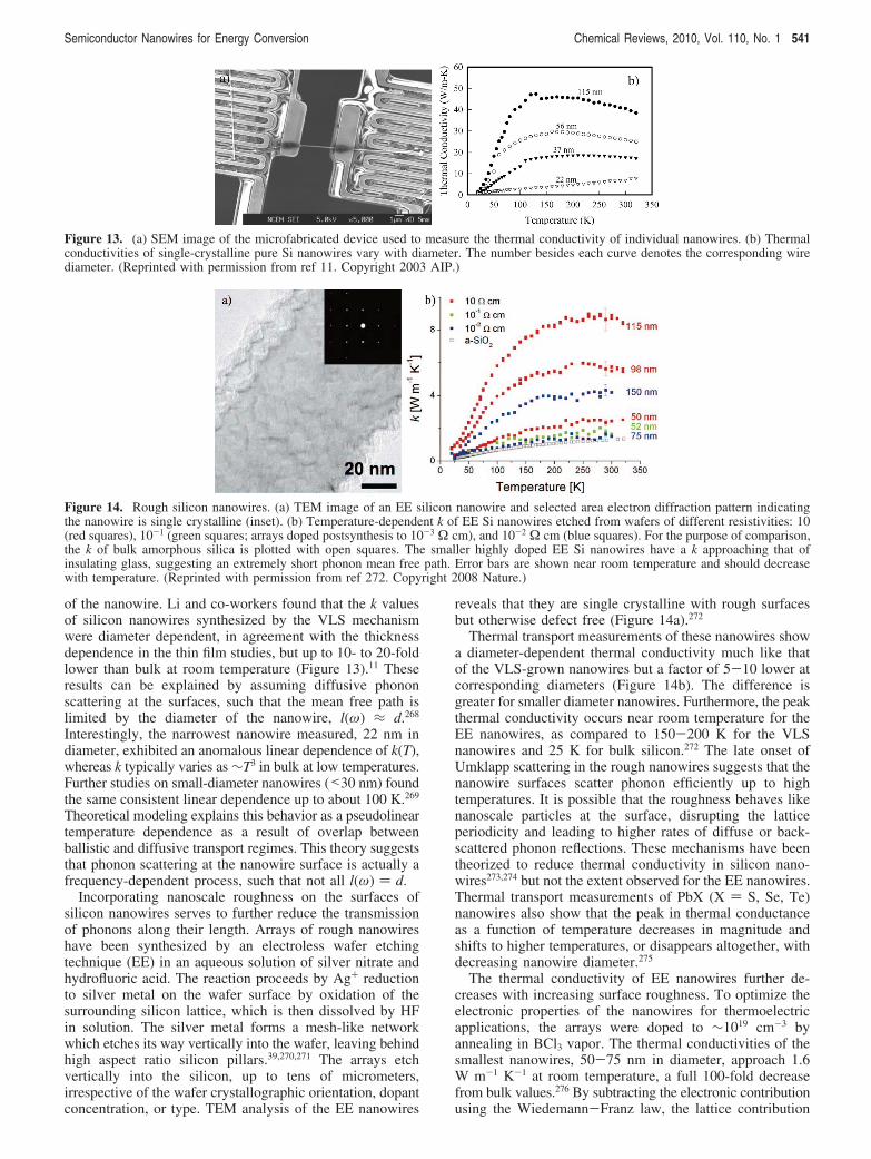
of the nanowire. Li and co-workers found that the k valuesof silicon nanowires synthesized by the VLS mechanismwere diameter dependent, in agreement with the thicknessdependence in the thin film studies, but up to 10- to 20-foldlower than bulk at room temperature (Figure 13).11 Theseresults can be explained by assuming diffusive phononscattering at the surfaces, such that the mean free path islimited by the diameter of the nanowire, l(ω) ≈ d.268
Interestingly, the narrowest nanowire measured, 22 nm indiameter, exhibited an anomalous linear dependence of k(T),whereas k typically varies as ∼T3 in bulk at low temperatures.Further studies on small-diameter nanowires (<30 nm) foundthe same consistent linear dependence up to about 100 K.269
Theoretical modeling explains this behavior as a pseudolineartemperature dependence as a result of overlap betweenballistic and diffusive transport regimes. This theory suggeststhat phonon scattering at the nanowire surface is actually afrequency-dependent process, such that not all l(ω) ) d.
Incorporating nanoscale roughness on the surfaces ofsilicon nanowires serves to further reduce the transmissionof phonons along their length. Arrays of rough nanowireshave been synthesized by an electroless wafer etchingtechnique (EE) in an aqueous solution of silver nitrate andhydrofluoric acid. The reaction proceeds by Ag+ reductionto silver metal on the wafer surface by oxidation of thesurrounding silicon lattice, which is then dissolved by HFin solution. The silver metal forms a mesh-like networkwhich etches its way vertically into the wafer, leaving behindhigh aspect ratio silicon pillars.39,270,271 The arrays etchvertically into the silicon, up to tens of micrometers,irrespective of the wafer crystallographic orientation, dopantconcentration, or type. TEM analysis of the EE nanowires
reveals that they are single crystalline with rough surfacesbut otherwise defect free (Figure 14a).272
Thermal transport measurements of these nanowires showa diameter-dependent thermal conductivity much like thatof the VLS-grown nanowires but a factor of 5-10 lower atcorresponding diameters (Figure 14b). The difference isgreater for smaller diameter nanowires. Furthermore, the peakthermal conductivity occurs near room temperature for theEE nanowires, as compared to 150-200 K for the VLSnanowires and 25 K for bulk silicon.272 The late onset ofUmklapp scattering in the rough nanowires suggests that thenanowire surfaces scatter phonon efficiently up to hightemperatures. It is possible that the roughness behaves likenanoscale particles at the surface, disrupting the latticeperiodicity and leading to higher rates of diffuse or back-scattered phonon reflections. These mechanisms have beentheorized to reduce thermal conductivity in silicon nano-wires273,274 but not the extent observed for the EE nanowires.Thermal transport measurements of PbX (X ) S, Se, Te)nanowires also show that the peak in thermal conductanceas a function of temperature decreases in magnitude andshifts to higher temperatures, or disappears altogether, withdecreasing nanowire diameter.275
The thermal conductivity of EE nanowires further de-creases with increasing surface roughness. To optimize theelectronic properties of the nanowires for thermoelectricapplications, the arrays were doped to ∼1019 cm-3 byannealing in BCl3 vapor. The thermal conductivities of thesmallest nanowires, 50-75 nm in diameter, approach 1.6W m-1 K-1 at room temperature, a full 100-fold decreasefrom bulk values.276 By subtracting the electronic contributionusing the Wiedemann-Franz law, the lattice contribution
Figure 13. (a) SEM image of the microfabricated device used to measure the thermal conductivity of individual nanowires. (b) Thermalconductivities of single-crystalline pure Si nanowires vary with diameter. The number besides each curve denotes the corresponding wirediameter. (Reprinted with permission from ref 11. Copyright 2003 AIP.)
Figure 14. Rough silicon nanowires. (a) TEM image of an EE silicon nanowire and selected area electron diffraction pattern indicatingthe nanowire is single crystalline (inset). (b) Temperature-dependent k of EE Si nanowires etched from wafers of different resistivities: 10(red squares), 10-1 (green squares; arrays doped postsynthesis to 10-3 Ω cm), and 10-2 Ω cm (blue squares). For the purpose of comparison,the k of bulk amorphous silica is plotted with open squares. The smaller highly doped EE Si nanowires have a k approaching that ofinsulating glass, suggesting an extremely short phonon mean free path. Error bars are shown near room temperature and should decreasewith temperature. (Reprinted with permission from ref 272. Copyright 2008 Nature.)
Semiconductor Nanowires for Energy Conversion Chemical Reviews, 2010, Vol. 110, No. 1 541
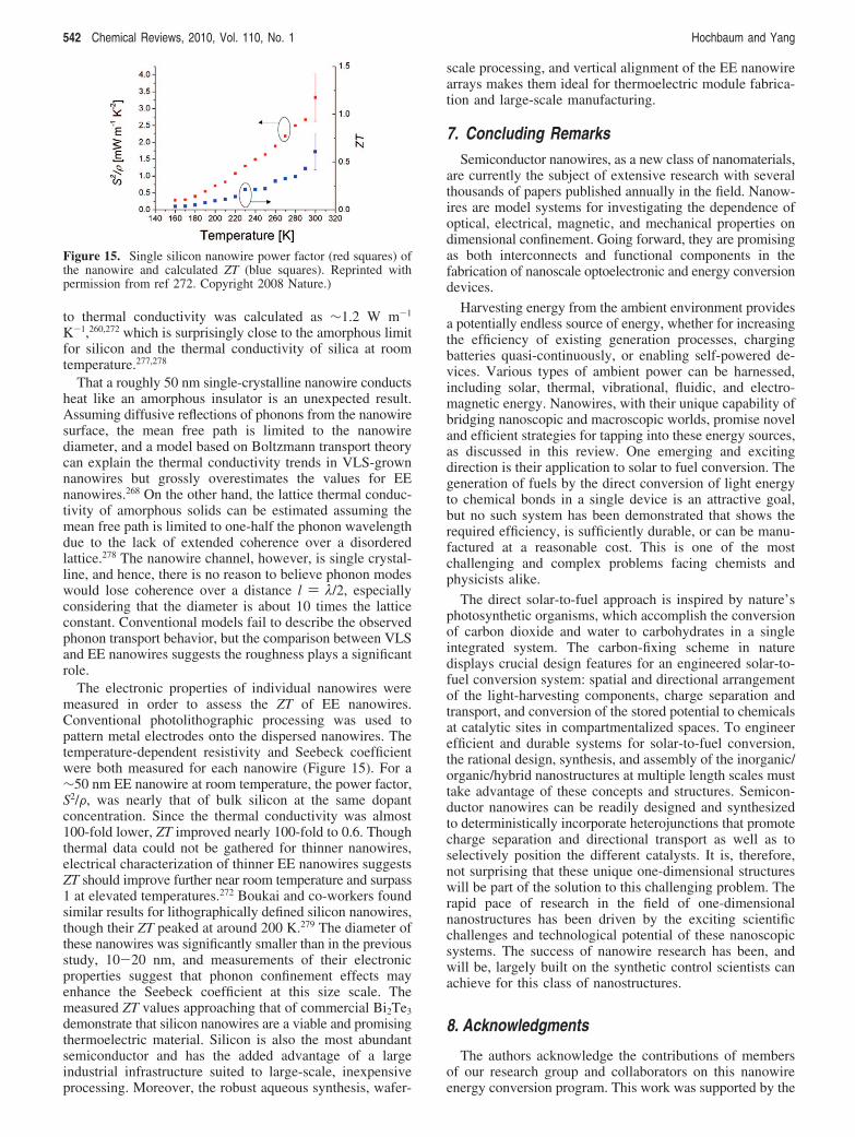
to thermal conductivity was calculated as ∼1.2 W m-1
K-1,260,272 which is surprisingly close to the amorphous limitfor silicon and the thermal conductivity of silica at roomtemperature.277,278
That a roughly 50 nm single-crystalline nanowire conductsheat like an amorphous insulator is an unexpected result.Assuming diffusive reflections of phonons from the nanowiresurface, the mean free path is limited to the nanowirediameter, and a model based on Boltzmann transport theorycan explain the thermal conductivity trends in VLS-grownnanowires but grossly overestimates the values for EEnanowires.268 On the other hand, the lattice thermal conduc-tivity of amorphous solids can be estimated assuming themean free path is limited to one-half the phonon wavelengthdue to the lack of extended coherence over a disorderedlattice.278 The nanowire channel, however, is single crystal-line, and hence, there is no reason to believe phonon modeswould lose coherence over a distance l ) λ/2, especiallyconsidering that the diameter is about 10 times the latticeconstant. Conventional models fail to describe the observedphonon transport behavior, but the comparison between VLSand EE nanowires suggests the roughness plays a significantrole.
The electronic properties of individual nanowires weremeasured in order to assess the ZT of EE nanowires.Conventional photolithographic processing was used topattern metal electrodes onto the dispersed nanowires. Thetemperature-dependent resistivity and Seebeck coefficientwere both measured for each nanowire (Figure 15). For a∼50 nm EE nanowire at room temperature, the power factor,S2/F, was nearly that of bulk silicon at the same dopantconcentration. Since the thermal conductivity was almost100-fold lower, ZT improved nearly 100-fold to 0.6. Thoughthermal data could not be gathered for thinner nanowires,electrical characterization of thinner EE nanowires suggestsZT should improve further near room temperature and surpass1 at elevated temperatures.272 Boukai and co-workers foundsimilar results for lithographically defined silicon nanowires,though their ZT peaked at around 200 K.279 The diameter ofthese nanowires was significantly smaller than in the previousstudy, 10-20 nm, and measurements of their electronicproperties suggest that phonon confinement effects mayenhance the Seebeck coefficient at this size scale. Themeasured ZT values approaching that of commercial Bi2Te3
demonstrate that silicon nanowires are a viable and promisingthermoelectric material. Silicon is also the most abundantsemiconductor and has the added advantage of a largeindustrial infrastructure suited to large-scale, inexpensiveprocessing. Moreover, the robust aqueous synthesis, wafer-
scale processing, and vertical alignment of the EE nanowirearrays makes them ideal for thermoelectric module fabrica-tion and large-scale manufacturing.
7. Concluding RemarksSemiconductor nanowires, as a new class of nanomaterials,
are currently the subject of extensive research with severalthousands of papers published annually in the field. Nanow-ires are model systems for investigating the dependence ofoptical, electrical, magnetic, and mechanical properties ondimensional confinement. Going forward, they are promisingas both interconnects and functional components in thefabrication of nanoscale optoelectronic and energy conversiondevices.
Harvesting energy from the ambient environment providesa potentially endless source of energy, whether for increasingthe efficiency of existing generation processes, chargingbatteries quasi-continuously, or enabling self-powered de-vices. Various types of ambient power can be harnessed,including solar, thermal, vibrational, fluidic, and electro-magnetic energy. Nanowires, with their unique capability ofbridging nanoscopic and macroscopic worlds, promise noveland efficient strategies for tapping into these energy sources,as discussed in this review. One emerging and excitingdirection is their application to solar to fuel conversion. Thegeneration of fuels by the direct conversion of light energyto chemical bonds in a single device is an attractive goal,but no such system has been demonstrated that shows therequired efficiency, is sufficiently durable, or can be manu-factured at a reasonable cost. This is one of the mostchallenging and complex problems facing chemists andphysicists alike.
The direct solar-to-fuel approach is inspired by nature’sphotosynthetic organisms, which accomplish the conversionof carbon dioxide and water to carbohydrates in a singleintegrated system. The carbon-fixing scheme in naturedisplays crucial design features for an engineered solar-to-fuel conversion system: spatial and directional arrangementof the light-harvesting components, charge separation andtransport, and conversion of the stored potential to chemicalsat catalytic sites in compartmentalized spaces. To engineerefficient and durable systems for solar-to-fuel conversion,the rational design, synthesis, and assembly of the inorganic/organic/hybrid nanostructures at multiple length scales musttake advantage of these concepts and structures. Semicon-ductor nanowires can be readily designed and synthesizedto deterministically incorporate heterojunctions that promotecharge separation and directional transport as well as toselectively position the different catalysts. It is, therefore,not surprising that these unique one-dimensional structureswill be part of the solution to this challenging problem. Therapid pace of research in the field of one-dimensionalnanostructures has been driven by the exciting scientificchallenges and technological potential of these nanoscopicsystems. The success of nanowire research has been, andwill be, largely built on the synthetic control scientists canachieve for this class of nanostructures.
8. Acknowledgments
The authors acknowledge the contributions of membersof our research group and collaborators on this nanowireenergy conversion program. This work was supported by the
Figure 15. Single silicon nanowire power factor (red squares) ofthe nanowire and calculated ZT (blue squares). Reprinted withpermission from ref 272. Copyright 2008 Nature.)
542 Chemical Reviews, 2010, Vol. 110, No. 1 Hochbaum and Yang
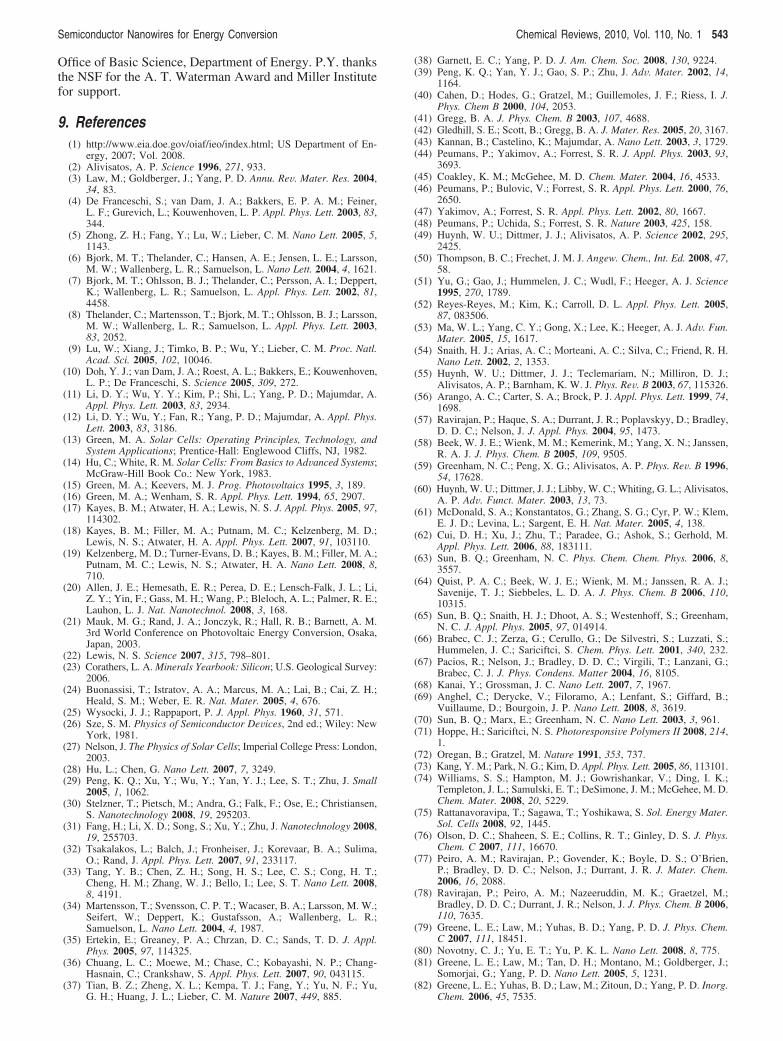
Office of Basic Science, Department of Energy. P.Y. thanksthe NSF for the A. T. Waterman Award and Miller Institutefor support.
9. References(1) http://www.eia.doe.gov/oiaf/ieo/index.html; US Department of En-
ergy, 2007; Vol. 2008.(2) Alivisatos, A. P. Science 1996, 271, 933.(3) Law, M.; Goldberger, J.; Yang, P. D. Annu. ReV. Mater. Res. 2004,
34, 83.(4) De Franceschi, S.; van Dam, J. A.; Bakkers, E. P. A. M.; Feiner,
L. F.; Gurevich, L.; Kouwenhoven, L. P. Appl. Phys. Lett. 2003, 83,344.
(5) Zhong, Z. H.; Fang, Y.; Lu, W.; Lieber, C. M. Nano Lett. 2005, 5,1143.
(6) Bjork, M. T.; Thelander, C.; Hansen, A. E.; Jensen, L. E.; Larsson,M. W.; Wallenberg, L. R.; Samuelson, L. Nano Lett. 2004, 4, 1621.
(7) Bjork, M. T.; Ohlsson, B. J.; Thelander, C.; Persson, A. I.; Deppert,K.; Wallenberg, L. R.; Samuelson, L. Appl. Phys. Lett. 2002, 81,4458.
(8) Thelander, C.; Martensson, T.; Bjork, M. T.; Ohlsson, B. J.; Larsson,M. W.; Wallenberg, L. R.; Samuelson, L. Appl. Phys. Lett. 2003,83, 2052.
(9) Lu, W.; Xiang, J.; Timko, B. P.; Wu, Y.; Lieber, C. M. Proc. Natl.Acad. Sci. 2005, 102, 10046.
(10) Doh, Y. J.; van Dam, J. A.; Roest, A. L.; Bakkers, E.; Kouwenhoven,L. P.; De Franceschi, S. Science 2005, 309, 272.
(11) Li, D. Y.; Wu, Y. Y.; Kim, P.; Shi, L.; Yang, P. D.; Majumdar, A.Appl. Phys. Lett. 2003, 83, 2934.
(12) Li, D. Y.; Wu, Y.; Fan, R.; Yang, P. D.; Majumdar, A. Appl. Phys.Lett. 2003, 83, 3186.
(13) Green, M. A. Solar Cells: Operating Principles, Technology, andSystem Applications; Prentice-Hall: Englewood Cliffs, NJ, 1982.
(14) Hu, C.; White, R. M. Solar Cells: From Basics to AdVanced Systems;McGraw-Hill Book Co.: New York, 1983.
(15) Green, M. A.; Keevers, M. J. Prog. PhotoVoltaics 1995, 3, 189.(16) Green, M. A.; Wenham, S. R. Appl. Phys. Lett. 1994, 65, 2907.(17) Kayes, B. M.; Atwater, H. A.; Lewis, N. S. J. Appl. Phys. 2005, 97,
114302.(18) Kayes, B. M.; Filler, M. A.; Putnam, M. C.; Kelzenberg, M. D.;
Lewis, N. S.; Atwater, H. A. Appl. Phys. Lett. 2007, 91, 103110.(19) Kelzenberg, M. D.; Turner-Evans, D. B.; Kayes, B. M.; Filler, M. A.;
Putnam, M. C.; Lewis, N. S.; Atwater, H. A. Nano Lett. 2008, 8,710.
(20) Allen, J. E.; Hemesath, E. R.; Perea, D. E.; Lensch-Falk, J. L.; Li,Z. Y.; Yin, F.; Gass, M. H.; Wang, P.; Bleloch, A. L.; Palmer, R. E.;Lauhon, L. J. Nat. Nanotechnol. 2008, 3, 168.
(21) Mauk, M. G.; Rand, J. A.; Jonczyk, R.; Hall, R. B.; Barnett, A. M.3rd World Conference on Photovoltaic Energy Conversion, Osaka,Japan, 2003.
(22) Lewis, N. S. Science 2007, 315, 798–801.(23) Corathers, L. A. Minerals Yearbook: Silicon; U.S. Geological Survey:
2006.(24) Buonassisi, T.; Istratov, A. A.; Marcus, M. A.; Lai, B.; Cai, Z. H.;
Heald, S. M.; Weber, E. R. Nat. Mater. 2005, 4, 676.(25) Wysocki, J. J.; Rappaport, P. J. Appl. Phys. 1960, 31, 571.(26) Sze, S. M. Physics of Semiconductor DeVices, 2nd ed.; Wiley: New
York, 1981.(27) Nelson, J. The Physics of Solar Cells; Imperial College Press: London,
2003.(28) Hu, L.; Chen, G. Nano Lett. 2007, 7, 3249.(29) Peng, K. Q.; Xu, Y.; Wu, Y.; Yan, Y. J.; Lee, S. T.; Zhu, J. Small
2005, 1, 1062.(30) Stelzner, T.; Pietsch, M.; Andra, G.; Falk, F.; Ose, E.; Christiansen,
S. Nanotechnology 2008, 19, 295203.(31) Fang, H.; Li, X. D.; Song, S.; Xu, Y.; Zhu, J. Nanotechnology 2008,
19, 255703.(32) Tsakalakos, L.; Balch, J.; Fronheiser, J.; Korevaar, B. A.; Sulima,
O.; Rand, J. Appl. Phys. Lett. 2007, 91, 233117.(33) Tang, Y. B.; Chen, Z. H.; Song, H. S.; Lee, C. S.; Cong, H. T.;
Cheng, H. M.; Zhang, W. J.; Bello, I.; Lee, S. T. Nano Lett. 2008,8, 4191.
(34) Martensson, T.; Svensson, C. P. T.; Wacaser, B. A.; Larsson, M. W.;Seifert, W.; Deppert, K.; Gustafsson, A.; Wallenberg, L. R.;Samuelson, L. Nano Lett. 2004, 4, 1987.
(35) Ertekin, E.; Greaney, P. A.; Chrzan, D. C.; Sands, T. D. J. Appl.Phys. 2005, 97, 114325.
(36) Chuang, L. C.; Moewe, M.; Chase, C.; Kobayashi, N. P.; Chang-Hasnain, C.; Crankshaw, S. Appl. Phys. Lett. 2007, 90, 043115.
(37) Tian, B. Z.; Zheng, X. L.; Kempa, T. J.; Fang, Y.; Yu, N. F.; Yu,G. H.; Huang, J. L.; Lieber, C. M. Nature 2007, 449, 885.
(38) Garnett, E. C.; Yang, P. D. J. Am. Chem. Soc. 2008, 130, 9224.(39) Peng, K. Q.; Yan, Y. J.; Gao, S. P.; Zhu, J. AdV. Mater. 2002, 14,
1164.(40) Cahen, D.; Hodes, G.; Gratzel, M.; Guillemoles, J. F.; Riess, I. J.
Phys. Chem B 2000, 104, 2053.(41) Gregg, B. A. J. Phys. Chem. B 2003, 107, 4688.(42) Gledhill, S. E.; Scott, B.; Gregg, B. A. J. Mater. Res. 2005, 20, 3167.(43) Kannan, B.; Castelino, K.; Majumdar, A. Nano Lett. 2003, 3, 1729.(44) Peumans, P.; Yakimov, A.; Forrest, S. R. J. Appl. Phys. 2003, 93,
3693.(45) Coakley, K. M.; McGehee, M. D. Chem. Mater. 2004, 16, 4533.(46) Peumans, P.; Bulovic, V.; Forrest, S. R. Appl. Phys. Lett. 2000, 76,
2650.(47) Yakimov, A.; Forrest, S. R. Appl. Phys. Lett. 2002, 80, 1667.(48) Peumans, P.; Uchida, S.; Forrest, S. R. Nature 2003, 425, 158.(49) Huynh, W. U.; Dittmer, J. J.; Alivisatos, A. P. Science 2002, 295,
2425.(50) Thompson, B. C.; Frechet, J. M. J. Angew. Chem., Int. Ed. 2008, 47,
58.(51) Yu, G.; Gao, J.; Hummelen, J. C.; Wudl, F.; Heeger, A. J. Science
1995, 270, 1789.(52) Reyes-Reyes, M.; Kim, K.; Carroll, D. L. Appl. Phys. Lett. 2005,
87, 083506.(53) Ma, W. L.; Yang, C. Y.; Gong, X.; Lee, K.; Heeger, A. J. AdV. Fun.
Mater. 2005, 15, 1617.(54) Snaith, H. J.; Arias, A. C.; Morteani, A. C.; Silva, C.; Friend, R. H.
Nano Lett. 2002, 2, 1353.(55) Huynh, W. U.; Dittmer, J. J.; Teclemariam, N.; Milliron, D. J.;
Alivisatos, A. P.; Barnham, K. W. J. Phys. ReV. B 2003, 67, 115326.(56) Arango, A. C.; Carter, S. A.; Brock, P. J. Appl. Phys. Lett. 1999, 74,
1698.(57) Ravirajan, P.; Haque, S. A.; Durrant, J. R.; Poplavskyy, D.; Bradley,
D. D. C.; Nelson, J. J. Appl. Phys. 2004, 95, 1473.(58) Beek, W. J. E.; Wienk, M. M.; Kemerink, M.; Yang, X. N.; Janssen,
R. A. J. J. Phys. Chem. B 2005, 109, 9505.(59) Greenham, N. C.; Peng, X. G.; Alivisatos, A. P. Phys. ReV. B 1996,
54, 17628.(60) Huynh, W. U.; Dittmer, J. J.; Libby, W. C.; Whiting, G. L.; Alivisatos,
A. P. AdV. Funct. Mater. 2003, 13, 73.(61) McDonald, S. A.; Konstantatos, G.; Zhang, S. G.; Cyr, P. W.; Klem,
E. J. D.; Levina, L.; Sargent, E. H. Nat. Mater. 2005, 4, 138.(62) Cui, D. H.; Xu, J.; Zhu, T.; Paradee, G.; Ashok, S.; Gerhold, M.
Appl. Phys. Lett. 2006, 88, 183111.(63) Sun, B. Q.; Greenham, N. C. Phys. Chem. Chem. Phys. 2006, 8,
3557.(64) Quist, P. A. C.; Beek, W. J. E.; Wienk, M. M.; Janssen, R. A. J.;
Savenije, T. J.; Siebbeles, L. D. A. J. Phys. Chem. B 2006, 110,10315.
(65) Sun, B. Q.; Snaith, H. J.; Dhoot, A. S.; Westenhoff, S.; Greenham,N. C. J. Appl. Phys. 2005, 97, 014914.
(66) Brabec, C. J.; Zerza, G.; Cerullo, G.; De Silvestri, S.; Luzzati, S.;Hummelen, J. C.; Sariciftci, S. Chem. Phys. Lett. 2001, 340, 232.
(67) Pacios, R.; Nelson, J.; Bradley, D. D. C.; Virgili, T.; Lanzani, G.;Brabec, C. J. J. Phys. Condens. Matter 2004, 16, 8105.
(68) Kanai, Y.; Grossman, J. C. Nano Lett. 2007, 7, 1967.(69) Anghel, C.; Derycke, V.; Filoramo, A.; Lenfant, S.; Giffard, B.;
Vuillaume, D.; Bourgoin, J. P. Nano Lett. 2008, 8, 3619.(70) Sun, B. Q.; Marx, E.; Greenham, N. C. Nano Lett. 2003, 3, 961.(71) Hoppe, H.; Sariciftci, N. S. PhotoresponsiVe Polymers II 2008, 214,
1.(72) Oregan, B.; Gratzel, M. Nature 1991, 353, 737.(73) Kang, Y. M.; Park, N. G.; Kim, D. Appl. Phys. Lett. 2005, 86, 113101.(74) Williams, S. S.; Hampton, M. J.; Gowrishankar, V.; Ding, I. K.;
Templeton, J. L.; Samulski, E. T.; DeSimone, J. M.; McGehee, M. D.Chem. Mater. 2008, 20, 5229.
(75) Rattanavoravipa, T.; Sagawa, T.; Yoshikawa, S. Sol. Energy Mater.Sol. Cells 2008, 92, 1445.
(76) Olson, D. C.; Shaheen, S. E.; Collins, R. T.; Ginley, D. S. J. Phys.Chem. C 2007, 111, 16670.
(77) Peiro, A. M.; Ravirajan, P.; Govender, K.; Boyle, D. S.; O’Brien,P.; Bradley, D. D. C.; Nelson, J.; Durrant, J. R. J. Mater. Chem.2006, 16, 2088.
(78) Ravirajan, P.; Peiro, A. M.; Nazeeruddin, M. K.; Graetzel, M.;Bradley, D. D. C.; Durrant, J. R.; Nelson, J. J. Phys. Chem. B 2006,110, 7635.
(79) Greene, L. E.; Law, M.; Yuhas, B. D.; Yang, P. D. J. Phys. Chem.C 2007, 111, 18451.
(80) Novotny, C. J.; Yu, E. T.; Yu, P. K. L. Nano Lett. 2008, 8, 775.(81) Greene, L. E.; Law, M.; Tan, D. H.; Montano, M.; Goldberger, J.;
Somorjai, G.; Yang, P. D. Nano Lett. 2005, 5, 1231.(82) Greene, L. E.; Yuhas, B. D.; Law, M.; Zitoun, D.; Yang, P. D. Inorg.
Chem. 2006, 45, 7535.
Semiconductor Nanowires for Energy Conversion Chemical Reviews, 2010, Vol. 110, No. 1 543
(83) Wang, G. M.; Swensen, J.; Moses, D.; Heeger, A. J. J. Appl. Phys.2003, 93, 6137.
(84) Chirvase, D.; Chiguvare, Z.; Knipper, M.; Parisi, J.; Dyakonov, V.;Hummelen, J. C. J. Appl. Phys. 2003, 93, 3376.
(85) Kroeze, J. E.; Savenije, T. J.; Vermeulen, M. J. W.; Warman, J. M.J. Phys. Chem. B 2003, 107, 7696.
(86) Plank, N. O. V.; Snaith, H. J.; Ducati, C.; Bendall, J. S.; Schmidt-Mende, L.; Welland, M. E. Nanotechnology 2008, 19, 465603.
(87) Coakley, K. M.; Srinivasan, B. S.; Ziebarth, J. M.; Goh, C.; Liu,Y. X.; McGehee, M. D. AdV. Funct. Mater. 2005, 15, 1927.
(88) Olson, D. C.; Piris, J.; Collins, R. T.; Shaheen, S. E.; Ginley, D. S.Thin Solid Films 2006, 496, 26.
(89) Takanezawa, K.; Hirota, K.; Wei, Q. S.; Tajima, K.; Hashimoto, K.J. Phys. Chem. C 2007, 111, 7218.
(90) Takanezawa, K.; Tajima, K.; Hashimoto, K. Appl. Phys. Lett. 2008,93, 063308.
(91) Gratzel, M. Nature 2001, 414, 338.(92) Chiba, Y.; Islam, A.; Watanabe, Y.; Komiya, R.; Koide, N.; Han,
L. Y. Jpn. J. Appl. Phys., Part 2: Lett. Expr. Lett. 2006, 45, L638.(93) Kroon, J. M.; Bakker, N. J.; Smit, H. J. P.; Liska, P.; Thampi, K. R.;
Wang, P.; Zakeeruddin, S. M.; Gratzel, M.; Hinsch, A.; Hore, S.;Wurfel, U.; Sastrawan, R.; Durrant, J. R.; Palomares, E.; Pettersson,H.; Gruszecki, T.; Walter, J.; Skupien, K.; Tulloch, G. E. Prog.PhotoVoltaics 2007, 15, 1.
(94) Wang, P.; Zakeeruddin, S. M.; Moser, J. E.; Nazeeruddin, M. K.;Sekiguchi, T.; Gratzel, M. Nat. Mater. 2003, 2, 402.
(95) Rensmo, H.; Keis, K.; Lindstrom, H.; Sodergren, S.; Solbrand, A.;Hagfeldt, A.; Lindquist, S. E.; Wang, L. N.; Muhammed, M. J. Phys.Chem. B 1997, 101, 2598.
(96) Tennakone, K.; Kumara, G. R. R. A.; Kottegoda, I. R. M.; Perera,V. P. S. Chem. Commun. 1999, 15.
(97) Keis, K.; Magnusson, E.; Lindstrom, H.; Lindquist, S. E.; Hagfeldt,A. Sol. Energy Mater. Sol. Cells 2002, 73, 51.
(98) Solbrand, A.; Keis, K.; Sodergren, S.; Lindstrom, H.; Lindquist, S. E.;Hagfeldt, A. Sol. Energy Mater. Sol. Cells 2000, 60, 181.
(99) Fisher, A. C.; Peter, L. M.; Ponomarev, E. A.; Walker, A. B.;Wijayantha, K. G. U. J. Phys. Chem. B 2000, 104, 949.
(100) Green, A. N. M.; Palomares, E.; Haque, S. A.; Kroon, J. M.; Durrant,J. R. J. Phys. Chem. B 2005, 109, 12525.
(101) Rensmo, H.; Lindstrom, H.; Sodergren, S.; Willstedt, A. K.; Solbrand,A.; Hagfeldt, A.; Lindquist, S. E. J. Electrochem. Soc. 1996, 143,3173.
(102) Lindstrom, H.; Rensmo, H.; Sodergren, S.; Solbrand, A.; Lindquist,S. E. J. Phys. Chem. 1996, 100, 3084.
(103) Sodergren, S.; Hagfeldt, A.; Olsson, J.; Lindquist, S. E. J. Phys. Chem.1994, 98, 5552.
(104) van de Lagemaat, J.; Park, N. G.; Frank, A. J. J. Phys. Chem. B2000, 104, 2044.
(105) Oekermann, T.; Zhang, D.; Yoshida, T.; Minoura, H. J. Phys. Chem.B 2004, 108, 2227.
(106) Nelson, J. Phys. ReV. B 1999, 59, 15374.(107) van de Lagemaat, J.; Frank, A. J. J. Phys. Chem. B 2001, 105, 11194.(108) Kopidakis, N.; Schiff, E. A.; Park, N. G.; van de Lagemaat, J.; Frank,
A. J. J. Phys. Chem. B 2000, 104, 3930.(109) Noack, V.; Weller, H.; Eychmuller, A. J. Phys. Chem. B 2002, 106,
8514.(110) Galoppini, E.; Rochford, J.; Chen, H. H.; Saraf, G.; Lu, Y. C.;
Hagfeldt, A.; Boschloo, G. J. Phys. Chem. B 2006, 110, 16159.(111) Enache-Pommer, E.; Boercker, J. E.; Aydil, E. S. Appl. Phys. Lett.
2007, 91, 123116.(112) Wang, Q.; Moser, J. E.; Gratzel, M. J. Phys. Chem. B 2005, 109,
14945.(113) Adachi, M.; Sakamoto, M.; Jiu, J. T.; Ogata, Y.; Isoda, S. J. Phys.
Chem. B 2006, 110, 13872.(114) Kavan, L.; Gratzel, M.; Gilbert, S. E.; Klemenz, C.; Scheel, H. J.
J. Am. Chem. Soc. 1996, 118, 6716.(115) Wagner, P.; Helbig, R. J. Phys. Chem. Solids 1974, 35, 327.(116) Nazeeruddin, M. K.; Pechy, P.; Renouard, T.; Zakeeruddin, S. M.;
Humphry-Baker, R.; Comte, P.; Liska, P.; Cevey, L.; Costa, E.;Shklover, V.; Spiccia, L.; Deacon, G. B.; Bignozzi, C. A.; Gratzel,M. J. Am. Chem. Soc. 2001, 123, 1613.
(117) Nakade, S.; Matsuda, M.; Kambe, S.; Saito, Y.; Kitamura, T.; Sakata,T.; Wada, Y.; Mori, H.; Yanagida, S. J. Phys. Chem. B 2002, 106,10004.
(118) Robertson, N. Angew. Chem., Int. Ed. 2006, 45, 2338.(119) Renouard, T.; Fallahpour, R. A.; Nazeeruddin, M. K.; Humphry-
Baker, R.; Gorelsky, S. I.; Lever, A. B. P.; Gratzel, M. Inorg. Chem.2002, 41, 367.
(120) Hara, K.; Kurashige, M.; Dan-oh, Y.; Kasada, C.; Shinpo, A.; Suga,S.; Sayama, K.; Arakawa, H. New J. Chem. 2003, 27, 783.
(121) Fan, S. H.; Wang, K. Z. Chin. J. Inorg. Chem. 2008, 24, 1206.(122) Bai, Y.; Cao, Y. M.; Zhang, J.; Wang, M.; Li, R. Z.; Wang, P.;
Zakeeruddin, S. M.; Gratzel, M. Nat. Mater. 2008, 7, 626.
(123) Gorlov, M.; Kloo, L. Dalton Trans. 2008, 2655.(124) Kron, G.; Egerter, T.; Werner, J. H.; Rau, U. J. Phys. Chem. B 2003,
107, 3556.(125) Thomas, D. G.; Lander, J. J. J. Chem. Phys. 1956, 25, 1136.(126) Greene, L. E.; Law, M.; Goldberger, J.; Kim, F.; Johnson, J. C.;
Zhang, Y. F.; Saykally, R. J.; Yang, P. D. Angew. Chem., Int. Ed.2003, 42, 3031.
(127) Law, M.; Greene, L. E.; Johnson, J. C.; Saykally, R.; Yang, P. D.Nat. Mater. 2005, 4, 455.
(128) Baxter, J. B.; Aydil, E. S. Appl. Phys. Lett. 2005, 86, 053114.(129) Nakade, S.; Saito, Y.; Kubo, W.; Kitamura, T.; Wada, Y.; Yanagida,
S. J. Phys. Chem. B 2003, 107, 8607.(130) Schumacher, J. O.; Wettling, W. In Clean Electricity from Photo-
Voltaics; Archer, M. D., Hill, R., Eds.; Imperial College Press:London, 2001.
(131) Tan, B.; Wu, Y. Y. J. Phys. Chem. B 2006, 110, 15932.(132) Ku, C. H.; Wu, J. J. Appl. Phys. Lett. 2007, 91, 093117.(133) Jiang, C. Y.; Sun, X. W.; Tan, K. W.; Lo, G. Q.; Kyaw, A. K. K.;
Kwong, D. L. Appl. Phys. Lett. 2008, 92, 143101.(134) Ku, C. H.; Wu, J. J. Nanotechnology 2007, 18, 505706.(135) Suh, D. I.; Lee, S. Y.; Kim, T. H.; Chun, J. M.; Suh, E. K.; Yang,
O. B.; Lee, S. K. Chem. Phys. Lett. 2007, 442, 348–353.(136) Baxter, J. B.; Walker, A. M.; van Ommering, K.; Aydil, E. S.
Nanotechnology 2006, 17, S304.(137) Horiuchi, H.; Katoh, R.; Hara, K.; Yanagida, M.; Murata, S.;
Arakawa, H.; Tachiya, M. J. Phys. Chem. B 2003, 107, 2570.(138) Keis, K.; Lindgren, J.; Lindquist, S. E.; Hagfeldt, A. Langmuir 2000,
16, 4688.(139) Oekermann, T.; Yoshida, T.; Minoura, H.; Wijayantha, K. G. U.;
Peter, L. M. J. Phys. Chem. B 2004, 108, 8364.(140) Liao, Z. M.; Xu, J.; Zhang, J. M.; Yu, D. P. Appl. Phys. Lett. 2008,
93, 023111.(141) Goldberger, J.; Sirbuly, D. J.; Law, M.; Yang, P. J. Phys. Chem. B
2005, 109, 9.(142) Elias, J.; Tena-Zaera, R.; Levy-Clement, C. Thin Solid Films 2007,
515, 8553.(143) Noh, J. H.; Lee, S. H.; Lee, S.; Jung, H. S. Electron. Mater. Lett.
2008, 4, 71.(144) Redmond, G.; Fitzmaurice, D.; Graetzel, M. Chem. Mater. 1994, 6,
686.(145) Wu, J. J.; Chen, G. R.; Yang, H. H.; Ku, C. H.; Lai, J. Y. Appl.
Phys. Lett. 2007, 90, 213109.(146) Law, M.; Greene, L. E.; Radenovic, A.; Kuykendall, T.; Liphardt,
J.; Yang, P. D. J. Phys. Chem. B 2006, 110, 22652.(147) Palomares, E.; Clifford, J. N.; Haque, S. A.; Lutz, T.; Durrant, J. R.
J. Am. Chem. Soc. 2003, 125, 475.(148) Gubbala, S.; Chakrapani, V.; Kumar, V.; Sunkara, M. K. AdV. Funct.
Mater. 2008, 18, 2411.(149) Joanni, E.; Savu, R.; Goes, M. D.; Bueno, P. R.; de Freitas, J. N.;
Nogueira, A. F.; Longo, E.; Varela, J. A. Scr. Mater. 2007, 57, 277.(150) Mor, G. K.; Shankar, K.; Paulose, M.; Varghese, O. K.; Grimes,
C. A. Nano Lett. 2006, 6, 215.(151) Zhu, K.; Vinzant, T. B.; Neale, N. R.; Frank, A. J. Nano Lett. 2007,
7, 3739.(152) Grimes, C. A.; Varghese, O. K.; Ranjan, S. Light, Water, Hydrogen:
The Solar Generation of Hydrogen by Water Photolysis; Springer:New York, 2008.
(153) Hou, K.; Tian, B. Z.; Li, F. Y.; Bian, Z. Q.; Zhao, D. Y.; Huang,C. H. J. Mater. Chem. 2005, 15, 2414.
(154) Zukalova, M.; Zukal, A.; Kavan, L.; Nazeeruddin, M. K.; Liska, P.;Gratzel, M. Nano Lett. 2005, 5, 1789.
(155) Zukalova, M.; Prochazka, J.; Zukal, A.; Yum, J. H.; Kavan, L. Inorg.Chim. Acta 2008, 361, 656.
(156) Adachi, M.; Murata, Y.; Takao, J.; Jiu, J. T.; Sakamoto, M.; Wang,F. M. J. Am. Chem. Soc. 2004, 126, 14943.
(157) Kopidakis, N.; Benkstein, K. D.; van de Lagemaat, J.; Frank, A. J.J. Phys. Chem. B 2003, 107, 11307.
(158) Feng, X. J.; Shankar, K.; Varghese, O. K.; Paulose, M.; Latempa,T. J.; Grimes, C. A. Nano Lett. 2008, 8, 3781.
(159) Liu, B.; Boercker, J. E.; Aydil, E. S. Nanotechnology 2008, 19,505604.
(160) Leschkies, K. S.; Divakar, R.; Basu, J.; Enache-Pommer, E.; Boercker,J. E.; Carter, C. B.; Kortshagen, U. R.; Norris, D. J.; Aydil, E. S.Nano Lett. 2007, 7, 1793.
(161) Levy-Clement, C.; Tena-Zaera, R.; Ryan, M. A.; Katty, A.; Hodes,G. AdV. Mater. 2005, 17, 1512.
(162) Tena-Zaera, R.; Katty, A.; Bastide, S.; Levy-Clement, C.; O’Regan,B.; Munoz-Sanjose, V. Thin Solid Films 2005, 483, 372.
(163) Whittingham, M. S. MRS Bull. 2008, 33, 411.(164) Linden, D. Handbook of Batteries, 1st ed.; McGraw-Hill: New York,
1995.(165) Ahn, K. S.; Shet, S.; Deutsch, T.; Jiang, C. S.; Yan, Y. F.; Al-Jassim,
M.; Turner, J. J. Power Sources 2008, 176, 387.
544 Chemical Reviews, 2010, Vol. 110, No. 1 Hochbaum and Yang
(166) Goodey, A. P.; Eichfeld, S. M.; Lew, K. K.; Redwing, J. M.; Mallouk,T. E. J. Am. Chem. Soc. 2007, 129, 12344.
(167) Guo, M.; Diao, P.; Cai, S. M. Appl. Surf. Sci. 2005, 249, 71.(168) Khan, S. U. M.; Sultana, T. Sol. Energy Mater. Sol. Cells 2003, 76,
211.(169) Maiolo, J. R.; Kayes, B. M.; Filler, M. A.; Putnam, M. C.; Kelzenberg,
M. D.; Atwater, H. A.; Lewis, N. S. J. Am. Chem. Soc. 2007, 129,12346.
(170) Peng, K. Q.; Wang, X.; Lee, S. T. Appl. Phys. Lett. 2008, 92, 163103.(171) Schierhorn, M.; Boettcher, S. W.; Ivanovskaya, A.; Norvell, E.;
Sherman, J. B.; Stucky, G. D.; Moskovits, M. J. Phys. Chem. C 2008,112, 8516.
(172) Spurgeon, J. M.; Atwater, H. A.; Lewis, N. S. J. Phys. Chem. C2008, 112, 6186.
(173) Yang, S. F.; Wen, X. G.; Zhang, W. X.; Yang, S. H. J. Electrochem.Soc. 2005, 152, G220.
(174) Wang, R. Y.; Feser, J. P.; Lee, J. S.; Talapin, D. V.; Segalman, R.;Majumdar, A. Nano Lett. 2008, 8, 2283.
(175) Nam, K. T.; Kim, D. W.; Yoo, P. J.; Chiang, C. Y.; Meethong, N.;Hammond, P. T.; Chiang, Y. M.; Belcher, A. M. Science 2006, 312,885.
(176) Guo, Y. G.; Hu, J. S.; Wan, L. J. AdV. Mater. 2008, 20, 2878.(177) Meethong, N.; Huang, H. Y. S.; Carter, W. C.; Chiang, Y. M.
Electrochem. Solid State Lett. 2007, 10, A134.(178) Meethong, N.; Kao, Y. H.; Tang, M.; Huang, H. Y.; Carter, W. C.;
Chiang, Y. M. Chem. Mater. 2008, 20, 6189.(179) Yang, J.; Winter, M.; Besenhard, J. O. Solid State Ionics 1996, 90,
281.(180) Cheng, Y. T.; Verbrugge, M. W. J. Appl. Phys. 2008, 104, 083521.(181) Huggins, R. A.; Nix, W. D. Ionics 2000, 6, 57.(182) Poizot, P.; Laruelle, S.; Grugeon, S.; Dupont, L.; Tarascon, J. M.
Nature 2000, 407, 496.(183) Whittingham, M. S. Dalton Trans. 2008, 5424.(184) Ryu, J. H.; Kim, J. W.; Sung, Y. E.; Oh, S. M. Electrochem. Solid
State Lett. 2004, 7, A306.(185) Kasavajjula, U.; Wang, C. S.; Appleby, A. J. J. Power Sources 2007,
163, 1003.(186) Ohara, S.; Suzuki, J.; Sekine, K.; Takamura, T. J. Power Sources
2004, 136, 303.(187) Takamura, T.; Ohara, S.; Uehara, M.; Suzuki, J.; Sekine, K. J. Power
Sources 2004, 129, 96.(188) Uehara, M.; Suzuki, J.; Tamura, K.; Sekine, K.; Takamura, T. J.
Power Sources 2005, 146, 441.(189) Gao, B.; Sinha, S.; Fleming, L.; Zhou, O. AdV. Mater. 2001, 13,
816.(190) Chan, C. K.; Peng, H. L.; Liu, G.; McIlwrath, K.; Zhang, X. F.;
Huggins, R. A.; Cui, Y. Nat. Nanotechnol. 2008, 3, 31.(191) Chan, C. K.; Zhang, X. F.; Cui, Y. Nano Lett. 2008, 8, 307.(192) Cui, L. F.; Ruffo, R.; Chan, C. K.; Peng, H. L.; Cui, Y. Nano Lett.
2009, 9, 491.(193) Kim, H.; Cho, J. Nano Lett. 2008, 8, 3688.(194) Kim, H.; Han, B.; Choo, J.; Cho, J. Angew. Chem., Int. Ed. 2008,
47, 10151.(195) Li, N. C.; Mitchell, D. T.; Lee, K. P.; Martin, C. R. J. Electrochem.
Soc. 2003, 150, A979.(196) Li, N. C.; Martin, C. R. J. Electrochem. Soc. 2001, 148, A164.(197) Park, M. S.; Wang, G. X.; Kang, Y. M.; Wexler, D.; Dou, S. X.;
Liu, H. K. Angew. Chem., Int. Ed. 2007, 46, 750.(198) Aragon, M. J.; Leon, B.; Vicente, C. P.; Tirado, J. L. Inorg. Chem.
2008, 47, 10366.(199) Armstrong, A. R.; Armstrong, G.; Canales, J.; Bruce, P. G. Angew.
Chem., Int. Ed. 2004, 43, 2286.(200) Armstrong, A. R.; Armstrong, G.; Canales, J.; Garcia, R.; Bruce,
P. G. AdV. Mater. 2005, 17, 862.(201) Armstrong, G.; Armstrong, A. R.; Bruce, P. G.; Reale, P.; Scrosati,
B. AdV. Mater. 2006, 18, 2597.(202) Li, Y. G.; Tan, B.; Wu, Y. Y. Nano Lett. 2008, 8, 265.(203) Lou, X. W.; Deng, D.; Lee, J. Y.; Feng, J.; Archer, L. A. AdV. Mater.
2008, 20, 258.(204) Shaju, K. M.; Jiao, F.; Debart, A.; Bruce, P. G. Phys. Chem. Chem.
Phys. 2007, 9, 1837.(205) Taberna, L.; Mitra, S.; Poizot, P.; Simon, P.; Tarascon, J. M. Nat.
Mater. 2006, 5, 567.(206) Li, N. C.; Patrissi, C. J.; Che, G. L.; Martin, C. R. J. Electrochem.
Soc. 2000, 147, 2044.(207) Kim, D. K.; Muralidharan, P.; Lee, H. W.; Ruffo, R.; Yang, Y.; Chan,
C. K.; Peng, H.; Huggins, R. A.; Cui, Y. Nano Lett. 2008, 8, 3948.(208) Kim, Y. S.; Ahn, H. J.; Nam, S. H.; Lee, S. H.; Shim, H. S.; Kim,
W. B. Appl. Phys. Lett. 2008, 93, 103104.(209) Takahashi, K.; Limmer, S. J.; Wang, Y.; Cao, G. Z. J. Phys. Chem.
B 2004, 108, 9795.(210) Takahashi, K.; Wang, Y.; Cao, G. Z. Appl. Phys. Lett. 2005, 86,
053102.
(211) Takahashi, K.; Wang, Y.; Cao, G. Z. J. Phys. Chem. B 2005, 109,48.
(212) Wang, Y.; Takahashi, K.; Shang, H. M.; Cao, G. Z. J. Phys. Chem.B 2005, 109, 3085.
(213) Chan, C. K.; Peng, H. L.; Twesten, R. D.; Jarausch, K.; Zhang, X. F.;Cui, Y. Nano Lett. 2007, 7, 490.
(214) http://www.eia.doe.gov/oiaf/ieo/index.html; US Department of En-ergy, 2008.
(215) Peng, K.; Jie, J.; Zhang, W.; Lee, S. T. Appl. Phys. Lett. 2008, 93,033105.
(216) Heikes, R. R.; Ure, R. W. Thermoelectricity: Science and Engineer-ing; Interscience Publishers: New York, 1961.
(217) Rowe, D. M. CRC Handbook of Thermoelectricity; CRC Press LLC:Boca Raton, 1995.
(218) Majumdar, A. Science 2004, 303, 777.(219) Snyder, G. J.; Toberer, E. S. Nat. Mater. 2008, 7, 105.(220) Hicks, L. D.; Dresselhaus, M. S. Phys. ReV. B 1993, 47, 12727.(221) Hicks, L. D.; Dresselhaus, M. S. Phys. ReV. B 1993, 47, 16631.(222) Lin, Y. M.; Dresselhaus, M. S. Phys. ReV. B 2003, 68, 075304.(223) Humphrey, T. E.; Linke, H. Phys. ReV. Lett. 2005, 94, 096601.(224) Rabina, O.; Lin, Y. M.; Dresselhaus, M. S. Appl. Phys. Lett. 2001,
79, 81.(225) Mingo, N. Appl. Phys. Lett. 2004, 85, 5986.(226) Mingo, N. Appl. Phys. Lett. 2004, 84, 2652.(227) Hicks, L. D.; Harman, T. C.; Sun, X.; Dresselhaus, M. S. Phys. ReV.
B 1996, 53, 10493.(228) Lin, Y. M.; Rabin, O.; Cronin, S. B.; Ying, J. Y.; Dresselhaus, M. S.
Appl. Phys. Lett. 2002, 81, 2403.(229) Ohta, H.; Kim, S.; Mune, Y.; Mizoguchi, T.; Nomura, K.; Ohta, S.;
Nomura, T.; Nakanishi, Y.; Ikuhara, Y.; Hirano, M.; Hosono, H.;Koumoto, K. Nat. Mater. 2007, 6, 129.
(230) Boukai, A.; Xu, K.; Heath, J. R. AdV. Mater. 2006, 18, 864.(231) Grozav, A. D.; Condrea, E. J. Phys. Condens. Matter 2004, 16, 6507.(232) Heremans, J. P.; Thrush, C. M.; Morelli, D. T.; Wu, M. C. Phys.
ReV. Lett. 2002, 88, 216801.(233) Zhou, J. H.; Jin, C. G.; Seol, J. H.; Li, X. G.; Shi, L. Appl. Phys.
Lett. 2005, 87, 133109.(234) Liufu, S. C.; Chen, L. D.; Yao, Q.; Wang, C. F. Appl. Phys. Lett.
2007, 90, 112106.(235) Qiu, X. F.; Austin, L. N.; Muscarella, P. A.; Dyck, J. S.; Burda, C.
Angew. Chem., Int. Ed. 2006, 45, 5656.(236) Tai, G.; Zhou, B.; Guo, W. L. J. Phys. Chem. C 2008, 112, 11314.(237) Tai, G. A.; Guo, W. L.; Zhang, Z. H. Cryst. Growth Des. 2008, 8,
2906.(238) Zhang, G. Q.; Wang, W.; Li, X. G. AdV. Mater. 2008, 20, 3654.(239) Yan, Q. Y.; Chen, H.; Zhou, W. W.; Hng, H. H.; Boey, F. Y. C.;
Ma, J. Chem. Mater. 2008, 20, 6298.(240) Zhou, F.; Szczech, J.; Pettes, M. T.; Moore, A. L.; Jin, S.; Shi, L.
Nano Lett. 2007, 7, 1649.(241) Seol, J. H.; Moore, A. L.; Saha, S. K.; Zhou, F.; Shi, L.; Ye, Q. L.;
Scheffler, R.; Mingo, N.; Yamada, T. J. Appl. Phys. 2007, 101,023706.
(242) Zhou, F.; Seol, J. H.; Moore, A. L.; Shi, L.; Ye, Q. L.; Scheffler, R.J. Phys. Condens. Matter 2006, 18, 9651.
(243) Kantser, V. G.; Bejenari, I. M.; Meglei, D. F. Mater. Sci. Eng., C2006, 26, 1175.
(244) Liang, W. J.; Hochbaum, A. I.; Fardy, M.; Rabin, O.; Zhang, M. J.;Yang, P. D. Nano Lett. 2009, 9, 1689.
(245) Heremans, J. P.; Jovovic, V.; Toberer, E. S.; Saramat, A.; Kurosaki,K.; Charoenphakdee, A.; Yamanaka, S.; Snyder, G. J. Science 2008,321, 554.
(246) Harman, T. C.; Taylor, P. J.; Walsh, M. P.; LaForge, B. E. Science2002, 297, 2229.
(247) Hsu, K. F.; Loo, S.; Guo, F.; Chen, W.; Dyck, J. S.; Uher, C.; Hogan,T.; Polychroniadis, E. K.; Kanatzidis, M. G. Science 2004, 303, 818.
(248) Venkatasubramanian, R.; Siivola, E.; Colpitts, T.; O’Quinn, B. Nature2001, 413, 597.
(249) Androulakis, J.; Hsu, K. F.; Pcionek, R.; Kong, H.; Uher, C.;DAngelo, J. J.; Downey, A.; Hogan, T.; Kanatzidis, M. G. AdV.Mater. 2006, 18, 1170.
(250) Chen, G. Phys. ReV. B 1998, 57, 14958.(251) Brinson, M. E.; Dunstan, W. J. Phys., Part C: Solid State Phys. 1970,
3, 483.(252) Cahill, D. G.; Ford, W. K.; Goodson, K. E.; Mahan, G. D.; Majumdar,
A.; Maris, H. J.; Merlin, R.; Phillpot, S. R. J. Appl. Phys. 2003, 93,793.
(253) Weber, L.; Gmelin, E. Appl. Phys. A: Mater. Sci. Proc. 1991, 53,136.
(254) Ruf, T.; Henn, R. W.; Asen-Palmer, M.; Gmelin, E.; Cardona, M.;Pohl, H. J.; Devyatych, G. G.; Sennikov, P. G. Solid State Commun.2000, 115, 243.
(255) Nolas, G. S.; Sharp, J.; Goldsmid, H. J. Thermoelectrics: BasicPrinciples and New Materials DeVelopments; Springer: Berlin, 2001.
Semiconductor Nanowires for Energy Conversion Chemical Reviews, 2010, Vol. 110, No. 1 545
(256) Cahill, D. G.; Goodson, K.; Majumdar, A. J. Heat Transfer: Trans.ASME 2002, 124, 223.
(257) Asheghi, M.; Leung, Y. K.; Wong, S. S.; Goodson, K. E. Appl. Phys.Lett. 1997, 71, 1798.
(258) Asheghi, M.; Touzelbaev, M. N.; Goodson, K. E.; Leung, Y. K.;Wong, S. S. J. Heat Transfer: Trans. ASME 1998, 120, 30.
(259) Ju, Y. S.; Goodson, K. E. Appl. Phys. Lett. 1999, 74, 3005.(260) Ashcroft, N. W.; Mermin, N. D. Solid State Physics; Saunders College
Publishers: Fort Worth, TX, 1976.(261) Poudel, B.; Hao, Q.; Ma, Y.; Lan, Y. C.; Minnich, A.; Yu, B.; Yan,
X.; Wang, D. Z.; Muto, A.; Vashaee, D.; Chen, X. Y.; Liu, J. M.;Dresselhaus, M. S.; Chen, G.; Ren, Z. Science 2008, 320, 634.
(262) Cao, Y. Q.; Zhu, T. J.; Zhao, X. B.; Zhang, X. B.; Tu, J. P. Appl.Phys. A: Mater. Sci. Process. 2008, 92, 321.
(263) Zhao, X. B.; Ji, X. H.; Zhang, Y. H.; Zhu, T. J.; Tu, J. P.; Zhang,X. B. Appl. Phys. Lett. 2005, 86, 062111.
(264) Joshi, G.; Lee, H.; Lan, Y. C.; Wang, X. W.; Zhu, G. H.; Wang,D. Z.; Gould, R. W.; Cuff, D. C.; Tang, M. Y.; Dresselhaus, M. S.;Chen, G.; Ren, Z. F. Nano Lett. 2008, 8, 4670.
(265) Wang, X. W.; Lee, H.; Lan, Y. C.; Zhu, G. H.; Joshi, G.; Wang,D. Z.; Yang, J.; Muto, A. J.; Tang, M. Y.; Klatsky, J.; Song, S.;Dresselhaus, M. S.; Chen, G.; Ren, Z. F. Appl. Phys. Lett. 2008, 93,193121.
(266) Kim, W.; Zide, J.; Gossard, A.; Klenov, D.; Stemmer, S.; Shakouri,A.; Majumdar, A. Phys. ReV. Lett. 2006, 96, 045901.
(267) Shi, L.; Li, D. Y.; Yu, C. H.; Jang, W. Y.; Kim, D. Y.; Yao, Z.;Kim, P.; Majumdar, A. J. Heat Transfer: Trans. ASME 2003, 125,1209.
(268) Mingo, N.; Yang, L.; Li, D.; Majumdar, A. Nano Lett. 2003, 3, 1713.(269) Chen, R.; Hochbaum, A. I.; Murphy, P.; Moore, J.; Yang, P. D.;
Majumdar, A. Phys. ReV. Lett. 2008, 101, 105501.(270) Peng, K. Q.; Wu, Y.; Fang, H.; Zhong, X. Y.; Xu, Y.; Zhu, J. Angew.
Chem., Int. Ed. 2005, 44, 2737.(271) Peng, K. Q.; Yan, Y. J.; Gao, S. P.; Zhu, J. AdV. Funct. Mater. 2003,
13, 127.(272) Hochbaum, A. I.; Chen, R. K.; Delgado, R. D.; Liang, W. J.; Garnett,
E. C.; Najarian, M.; Majumdar, A.; Yang, P. D. Nature 2008, 451,163.
(273) Moore, A. L.; Saha, S. K.; Prasher, R. S.; Shi, L. Appl. Phys. Lett.2008, 93, 083112.
(274) Zou, J.; Balandin, A. J. Appl. Phys. 2001, 89, 2932.(275) Fardy, M.; Hochbaum, A. I.; Goldberger, J.; Zhang, M. M.; Yang,
P. D. AdV. Mater. 2007, 19, 3047.(276) Touloukian, Y. S.; Powell, R. W.; Ho, C. Y.; Klemens, P. G. Thermal
ConductiVity: Metallic Elements and Alloys; IFI/Plenum: New York,1970.
(277) Cahill, D. G.; Pohl, R. O. Phys. ReV. B 1987, 35, 4067.(278) Cahill, D. G.; Watson, S. K.; Pohl, R. O. Phys. ReV. B 1992, 46,
6131.(279) Boukai, A. I.; Bunimovich, Y.; Tahir-Kheli, J.; Yu, J. K.; Goddard,
W. A.; Heath, J. R. Nature 2008, 451, 168.
CR900075V
546 Chemical Reviews, 2010, Vol. 110, No. 1 Hochbaum and Yang
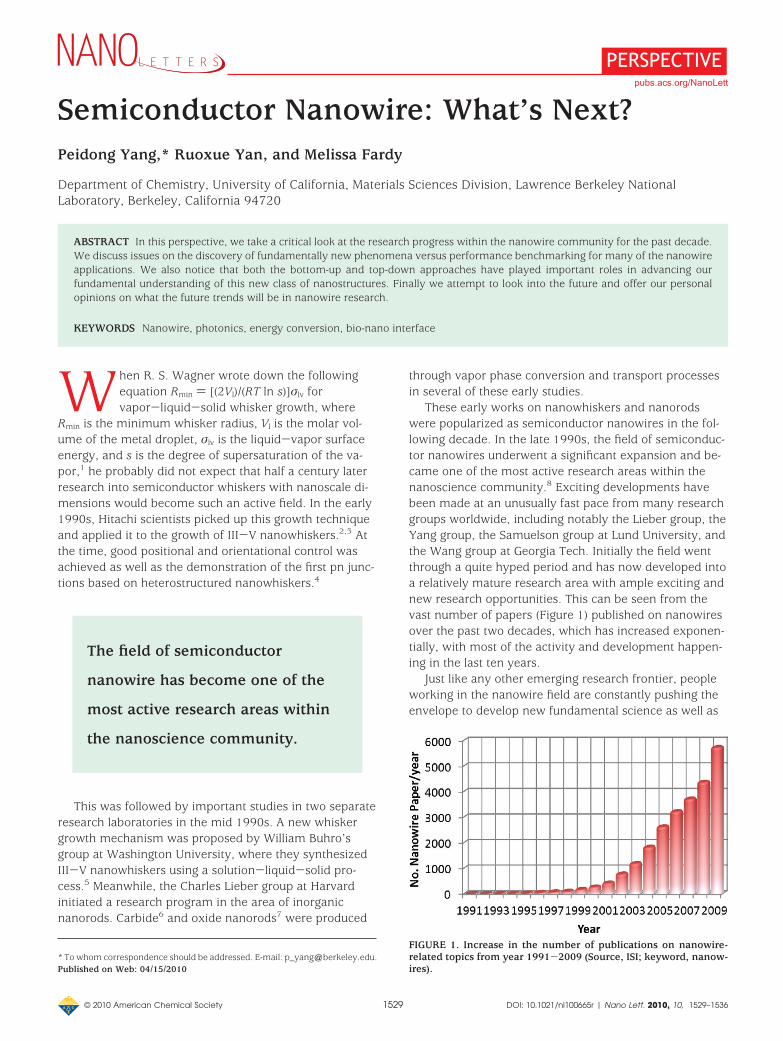
Semiconductor Nanowire: What’s Next?Peidong Yang,* Ruoxue Yan, and Melissa Fardy
Department of Chemistry, University of California, Materials Sciences Division, Lawrence Berkeley NationalLaboratory, Berkeley, California 94720
ABSTRACT In this perspective, we take a critical look at the research progress within the nanowire community for the past decade.We discuss issues on the discovery of fundamentally new phenomena versus performance benchmarking for many of the nanowireapplications. We also notice that both the bottom-up and top-down approaches have played important roles in advancing ourfundamental understanding of this new class of nanostructures. Finally we attempt to look into the future and offer our personalopinions on what the future trends will be in nanowire research.
KEYWORDS Nanowire, photonics, energy conversion, bio-nano interface
When R. S. Wagner wrote down the followingequation Rmin ) [(2Vl)/(RT ln s)]σlv forvapor-liquid-solid whisker growth, where
Rmin is the minimum whisker radius, Vl is the molar vol-ume of the metal droplet, σlv is the liquid-vapor surfaceenergy, and s is the degree of supersaturation of the va-por,1 he probably did not expect that half a century laterresearch into semiconductor whiskers with nanoscale di-mensions would become such an active field. In the early1990s, Hitachi scientists picked up this growth techniqueand applied it to the growth of III-V nanowhiskers.2,3 Atthe time, good positional and orientational control wasachieved as well as the demonstration of the first pn junc-tions based on heterostructured nanowhiskers.4
This was followed by important studies in two separateresearch laboratories in the mid 1990s. A new whiskergrowth mechanism was proposed by William Buhro’sgroup at Washington University, where they synthesizedIII-V nanowhiskers using a solution-liquid-solid pro-cess.5 Meanwhile, the Charles Lieber group at Harvardinitiated a research program in the area of inorganicnanorods. Carbide6 and oxide nanorods7 were produced
through vapor phase conversion and transport processesin several of these early studies.
These early works on nanowhiskers and nanorodswere popularized as semiconductor nanowires in the fol-lowing decade. In the late 1990s, the field of semiconduc-tor nanowires underwent a significant expansion and be-came one of the most active research areas within thenanoscience community.8 Exciting developments havebeen made at an unusually fast pace from many researchgroups worldwide, including notably the Lieber group, theYang group, the Samuelson group at Lund University, andthe Wang group at Georgia Tech. Initially the field wentthrough a quite hyped period and has now developed intoa relatively mature research area with ample exciting andnew research opportunities. This can be seen from thevast number of papers (Figure 1) published on nanowiresover the past two decades, which has increased exponen-tially, with most of the activity and development happen-ing in the last ten years.
Just like any other emerging research frontier, peopleworking in the nanowire field are constantly pushing theenvelope to develop new fundamental science as well as
* To whom correspondence should be addressed. E-mail: [email protected] on Web: 04/15/2010
The field of semiconductor
nanowire has become one of the
most active research areas within
the nanoscience community.
FIGURE 1. Increase in the number of publications on nanowire-related topics from year 1991-2009 (Source, ISI; keyword, nanow-ires).
PERSPECTIVEpubs.acs.org/NanoLett
© 2010 American Chemical Society 1529 DOI: 10.1021/nl100665r | Nano Lett. 2010, 10, 1529–1536
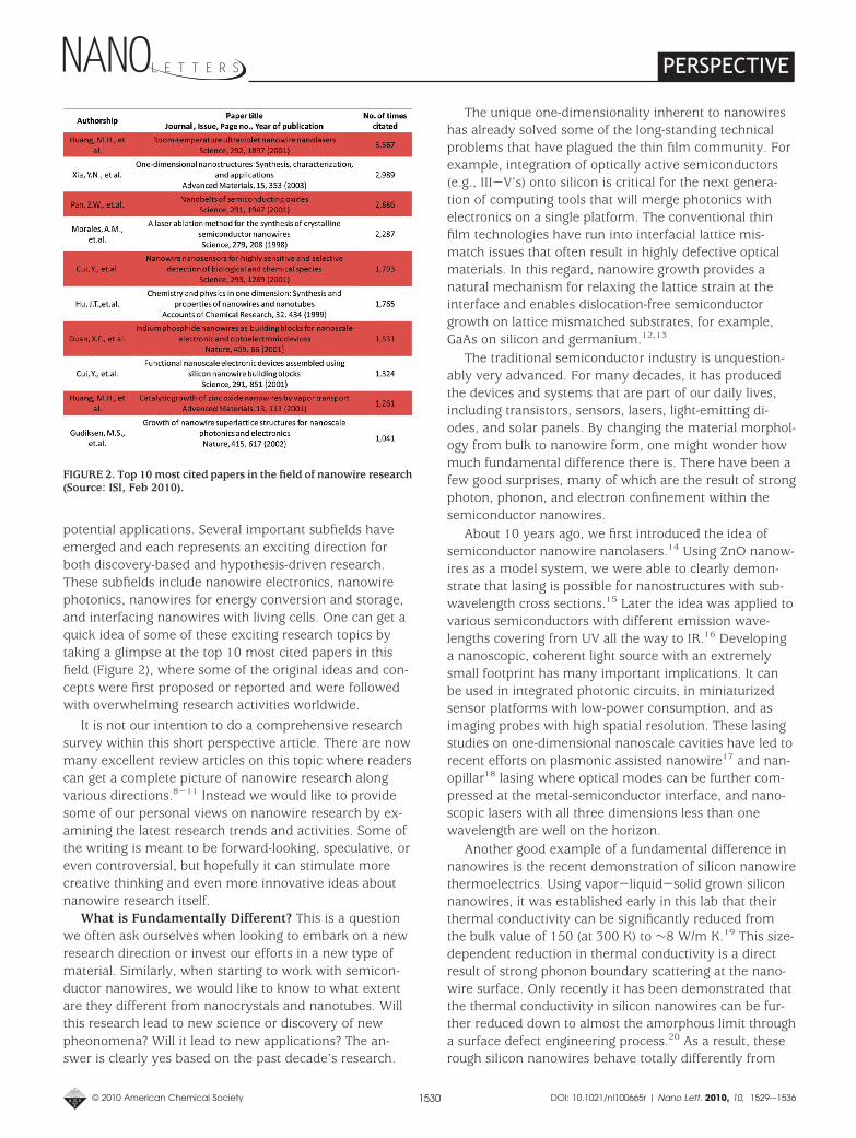
potential applications. Several important subfields haveemerged and each represents an exciting direction forboth discovery-based and hypothesis-driven research.These subfields include nanowire electronics, nanowirephotonics, nanowires for energy conversion and storage,and interfacing nanowires with living cells. One can get aquick idea of some of these exciting research topics bytaking a glimpse at the top 10 most cited papers in thisfield (Figure 2), where some of the original ideas and con-cepts were first proposed or reported and were followedwith overwhelming research activities worldwide.
It is not our intention to do a comprehensive researchsurvey within this short perspective article. There are nowmany excellent review articles on this topic where readerscan get a complete picture of nanowire research alongvarious directions.8-11 Instead we would like to providesome of our personal views on nanowire research by ex-amining the latest research trends and activities. Some ofthe writing is meant to be forward-looking, speculative, oreven controversial, but hopefully it can stimulate morecreative thinking and even more innovative ideas aboutnanowire research itself.
What is Fundamentally Different? This is a questionwe often ask ourselves when looking to embark on a newresearch direction or invest our efforts in a new type ofmaterial. Similarly, when starting to work with semicon-ductor nanowires, we would like to know to what extentare they different from nanocrystals and nanotubes. Willthis research lead to new science or discovery of newpheonomena? Will it lead to new applications? The an-swer is clearly yes based on the past decade’s research.
The unique one-dimensionality inherent to nanowireshas already solved some of the long-standing technicalproblems that have plagued the thin film community. Forexample, integration of optically active semiconductors(e.g., III-V’s) onto silicon is critical for the next genera-tion of computing tools that will merge photonics withelectronics on a single platform. The conventional thinfilm technologies have run into interfacial lattice mis-match issues that often result in highly defective opticalmaterials. In this regard, nanowire growth provides anatural mechanism for relaxing the lattice strain at theinterface and enables dislocation-free semiconductorgrowth on lattice mismatched substrates, for example,GaAs on silicon and germanium.12,13
The traditional semiconductor industry is unquestion-ably very advanced. For many decades, it has producedthe devices and systems that are part of our daily lives,including transistors, sensors, lasers, light-emitting di-odes, and solar panels. By changing the material morphol-ogy from bulk to nanowire form, one might wonder howmuch fundamental difference there is. There have been afew good surprises, many of which are the result of strongphoton, phonon, and electron confinement within thesemiconductor nanowires.
About 10 years ago, we first introduced the idea ofsemiconductor nanowire nanolasers.14 Using ZnO nanow-ires as a model system, we were able to clearly demon-strate that lasing is possible for nanostructures with sub-wavelength cross sections.15 Later the idea was applied tovarious semiconductors with different emission wave-lengths covering from UV all the way to IR.16 Developinga nanoscopic, coherent light source with an extremelysmall footprint has many important implications. It canbe used in integrated photonic circuits, in miniaturizedsensor platforms with low-power consumption, and asimaging probes with high spatial resolution. These lasingstudies on one-dimensional nanoscale cavities have led torecent efforts on plasmonic assisted nanowire17 and nan-opillar18 lasing where optical modes can be further com-pressed at the metal-semiconductor interface, and nano-scopic lasers with all three dimensions less than onewavelength are well on the horizon.
Another good example of a fundamental difference innanowires is the recent demonstration of silicon nanowirethermoelectrics. Using vapor-liquid-solid grown siliconnanowires, it was established early in this lab that theirthermal conductivity can be significantly reduced fromthe bulk value of 150 (at 300 K) to ∼8 W/m K.19 This size-dependent reduction in thermal conductivity is a directresult of strong phonon boundary scattering at the nano-wire surface. Only recently it has been demonstrated thatthe thermal conductivity in silicon nanowires can be fur-ther reduced down to almost the amorphous limit througha surface defect engineering process.20 As a result, theserough silicon nanowires behave totally differently from
FIGURE 2. Top 10 most cited papers in the field of nanowire research(Source: ISI, Feb 2010).
PERSPECTIVE
© 2010 American Chemical Society 1530 DOI: 10.1021/nl100665r | Nano Lett. 2010, 10, 1529-–1536
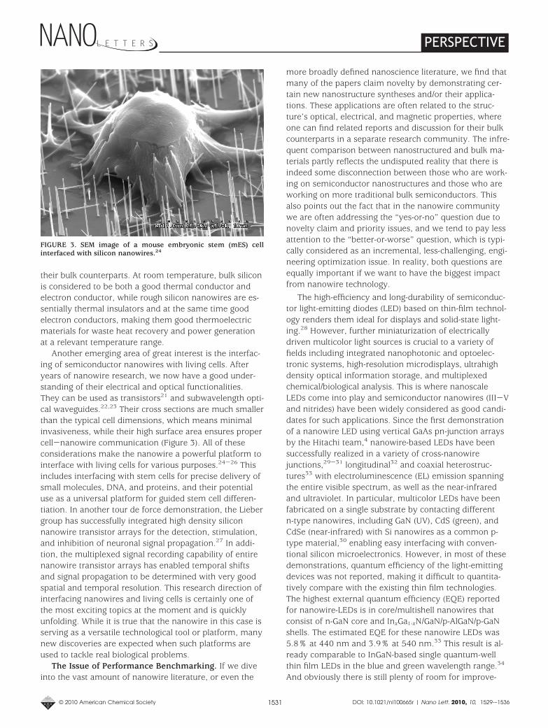
their bulk counterparts. At room temperature, bulk siliconis considered to be both a good thermal conductor andelectron conductor, while rough silicon nanowires are es-sentially thermal insulators and at the same time goodelectron conductors, making them good thermoelectricmaterials for waste heat recovery and power generationat a relevant temperature range.
Another emerging area of great interest is the interfac-ing of semiconductor nanowires with living cells. Afteryears of nanowire research, we now have a good under-standing of their electrical and optical functionalities.They can be used as transistors21 and subwavelength opti-cal waveguides.22,23 Their cross sections are much smallerthan the typical cell dimensions, which means minimalinvasiveness, while their high surface area ensures propercell-nanowire communication (Figure 3). All of theseconsiderations make the nanowire a powerful platform tointerface with living cells for various purposes.24-26 Thisincludes interfacing with stem cells for precise delivery ofsmall molecules, DNA, and proteins, and their potentialuse as a universal platform for guided stem cell differen-tiation. In another tour de force demonstration, the Liebergroup has successfully integrated high density siliconnanowire transistor arrays for the detection, stimulation,and inhibition of neuronal signal propagation.27 In addi-tion, the multiplexed signal recording capability of entirenanowire transistor arrays has enabled temporal shiftsand signal propagation to be determined with very goodspatial and temporal resolution. This research direction ofinterfacing nanowires and living cells is certainly one ofthe most exciting topics at the moment and is quicklyunfolding. While it is true that the nanowire in this case isserving as a versatile technological tool or platform, manynew discoveries are expected when such platforms areused to tackle real biological problems.
The Issue of Performance Benchmarking. If we diveinto the vast amount of nanowire literature, or even the
more broadly defined nanoscience literature, we find thatmany of the papers claim novelty by demonstrating cer-tain new nanostructure syntheses and/or their applica-tions. These applications are often related to the struc-ture’s optical, electrical, and magnetic properties, whereone can find related reports and discussion for their bulkcounterparts in a separate research community. The infre-quent comparison between nanostructured and bulk ma-terials partly reflects the undisputed reality that there isindeed some disconnection between those who are work-ing on semiconductor nanostructures and those who areworking on more traditional bulk semiconductors. Thisalso points out the fact that in the nanowire communitywe are often addressing the “yes-or-no” question due tonovelty claim and priority issues, and we tend to pay lessattention to the “better-or-worse” question, which is typi-cally considered as an incremental, less-challenging, engi-neering optimization issue. In reality, both questions areequally important if we want to have the biggest impactfrom nanowire technology.
The high-efficiency and long-durability of semiconduc-tor light-emitting diodes (LED) based on thin-film technol-ogy renders them ideal for displays and solid-state light-ing.28 However, further miniaturization of electricallydriven multicolor light sources is crucial to a variety offields including integrated nanophotonic and optoelec-tronic systems, high-resolution microdisplays, ultrahighdensity optical information storage, and multiplexedchemical/biological analysis. This is where nanoscaleLEDs come into play and semiconductor nanowires (III-Vand nitrides) have been widely considered as good candi-dates for such applications. Since the first demonstrationof a nanowire LED using vertical GaAs pn-junction arraysby the Hitachi team,4 nanowire-based LEDs have beensuccessfully realized in a variety of cross-nanowirejunctions,29-31 longitudinal32 and coaxial heterostruc-tures33 with electroluminescence (EL) emission spanningthe entire visible spectrum, as well as the near-infraredand ultraviolet. In particular, multicolor LEDs have beenfabricated on a single substrate by contacting differentn-type nanowires, including GaN (UV), CdS (green), andCdSe (near-infrared) with Si nanowires as a common p-type material,30 enabling easy interfacing with conven-tional silicon microelectronics. However, in most of thesedemonstrations, quantum efficiency of the light-emittingdevices was not reported, making it difficult to quantita-tively compare with the existing thin film technologies.The highest external quantum efficiency (EQE) reportedfor nanowire-LEDs is in core/multishell nanowires thatconsist of n-GaN core and InxGa1-xN/GaN/p-AlGaN/p-GaNshells. The estimated EQE for these nanowire LEDs was5.8% at 440 nm and 3.9% at 540 nm.33 This result is al-ready comparable to InGaN-based single quantum-wellthin film LEDs in the blue and green wavelength range.34
And obviously there is still plenty of room for improve-
FIGURE 3. SEM image of a mouse embryonic stem (mES) cellinterfaced with silicon nanowires.24
PERSPECTIVE
© 2010 American Chemical Society 1531 DOI: 10.1021/nl100665r | Nano Lett. 2010, 10, 1529-–1536
ment by optimizing collection efficiency and interfacecontrol to minimize undesired nonradiativerecombination.
A similar comparison can be made between nanowireand conventional thin-film solar cells. Solar cells are beingpursued as environmentally friendly, renewable powersources to ease the energy crisis currently confrontinghuman society. However, it remains a challenge to makeinexpensive, high-efficiency photovoltaic devices for largescale energy conversion. Semiconductor nanowires havebeen proposed to be fundamentally advantageous forphotovoltaic applications due to their unique properties.Some of the many advantages that nanowires offer in-clude long absorption path lengths while maintainingshort distances for carrier collection/transport; interpen-etrating heterojunction interfaces, allowing efficient car-rier extraction following light absorption; strong light trap-ping in high-density nanowire arrays; and modification ofmaterial properties and cell efficiencies through size andcomposition variation of the nanostructures. Dye-sensi-tized solar cells using dense arrays of oriented, crystallineZnO nanowires as the anode have been designed to im-prove charge collection efficiency.35 The direct electricalpathways provided by the nanowires ensure the rapidcollection of carriers generated throughout the device,and an efficiency of 2.5%36 under AM 1.5 illuminationhas been demonstrated, limited primarily by the need toimprove dye-loading by increasing the surface area of thenanowire array. Coaxial silicon nanowires (p-type/intrin-sic/n-type (p-i-n)) have achieved an apparent energy con-version efficiency of up to 3.4% under AM 1.5 illumina-tion and are able to drive functional nanoelectronicsensors and logic devices.37 And more recently, stronglight-trapping effects were observed in high-density siliconcore-shell nanowire array solar cells with efficiencies upto 6%.38 Integrated with ultralow power nanosystems,such as remote and mobile chemical and environmentalsensors, nanoelectronic and nanophotonic circuitry, thesenanowire-based photovoltaic devices may serve as cleanand sustainable miniature power sources. However, itremains a scientific challenge to design and synthesizenanowires and their heterostructures with performancesexceeding that of the existing silicon photovoltaic technol-ogy, which has a commercial efficiency larger than 20%and is being pushed to it is theoretical limiting efficiencyof 29%.39 Issues to be considered include surface recom-bination problems associated with the high surface areaof the nanowires.
A couple of years ago, a nanogenerator based on ZnOnanowires40 was developed to power battery-free wirelessnanodevices by converting ambient vibrations, hydraulicenergy, or mechanical movement to electricity. Thesedevices with their varying configurations41-44 demon-strate the capability of harvesting energy from ambientvibrations in different media,41,45 even from body and
muscle movements,46 and under a variety of frequencies(<10 Hz to 41 kHz).41,42 However, the major bottleneck tothe application of these nanogenerators is their low out-put power, which is usually on the order of nanowatts(areal power density <1 µW/cm2)43,47 and low output volt-age, which is dictated by individual nanowires and is typi-cally <100 mV.44,46,48,49 In comparison, a commercialpiezo generator based on piezoceramic thin films operat-ing in the same frequency range can be 3-4 orders ofmagnitude higher in these parameters (e.g., piezoelectricheel-strike generators50). Although different strategies toimprove the output power and voltage have been pro-posed,51 these nanogenerators may never be able topower our homes or even our flash lights. However, ZnOnanowire-based nanogenerators possess unique featuresthat make them promising solutions for independent, sus-tainable, maintenance-free nanosystems that have low-power consumption, such as implantable biosensors, nan-orobotics, and possibly portable/wearable personalelectronics.
While the previous section focused on the scientificbreakthroughs achieved by constantly pushing the funda-mental limits of nanowires, here we would like to makethe case that a technological breakthrough will come onlyafter we address both “yes-or-no” and “better-or-worse”issues with all of our undivided attention. Long-term sta-bility will also be a common problem for many of thenanowire-based devices and systems. It is true for theLEDs, solar cells, and piezoelectric generators we dis-cussed here, as well as sensors, batteries, and transistors.We need to keep in mind that all of these areas have ex-isting mature industrial technologies (largely technologiesbased on thin film and bulk semiconductors). Unless thereare significant cost and/or performance benefits from us-ing nanowires, it will be difficult to displace the existingtechnologies.
Bottom-up versus Top-down. There are now manydifferent methods for making semiconductor nanowires.They are commonly placed into two categories, namely,the bottom-up and top-down approaches. The bottom-upapproach starts with individual atoms and molecules andbuilds up the desired nanostructures. For nanowire syn-thesis, this includes vapor-liquid-solid (VLS) chemicalvapor deposition, the solid-liquid-solid process, nanop-ore templating, and various hydrothermal methods. Thetop-down approach relies on dimensional reductionthrough selective etching and various nanoimprintingtechniques. Similarly, for the integration of nanowirebuilding blocks, there are also two such general ap-proaches, the first being chemical assembly such asLangmuir-Blodgett techniques, the other being litho-graphical processes. So, which one is better?
The answer as of now is a bit of both. It is clear at thispoint that we need both approaches for many of the ap-plications related to semiconductor nanowires. Synthesis-
PERSPECTIVE
© 2010 American Chemical Society 1532 DOI: 10.1021/nl100665r | Nano Lett. 2010, 10, 1529-–1536
based bottom-up approaches can be used to generatestructures with dimensions ranging from angstroms tohundreds of nanometers. On the other hand, while thefabrication based top-down processes still have difficultycreating structures below 10 nm, they have a great advan-tage when integration and addressability are concerned.
There are a couple of good examples that illustrate thevalue of both strategies. The thermoelectric performanceof silicon nanowires has been examined in both syntheticand fabricated nanowires. The Yang group has focused onVLS grown and chemically etched nanowires20 while theHeath group has had great success with their SuperlatticeNanowire Pattern Transfer (SNAP) process to producevery thin silicon nanowires.52 In both cases, similar ther-moelectric performance was observed.
The concept of nanowire based solar cells has attractedsignificant attention because of their potential benefits incarrier transport, charge separation, and light absorption.The Lieber group has developed a fairly sophiscatedcore-sheath growth and contact strategy for their siliconp-i-n nanowire solar cells with efficiencies up to 3.5%.37
On the other hand, etching and overgrowth processeshave also been developed to fabricate high density siliconcore-shell solar cells. Efficiencies up to 6% have beendemonstrated in this type of top-down fabricated nano-wire core-shell arrays.38 Here, both synthetic and fabri-cated nanowires offer similar core-shell solar cell de-signs, and therefore the same operational principle, butwith differences in interface sharpness and carrier recom-bination kinetics.
We can find a similar situation when it comes to sen-sor and laser research. On the basis of chemically synthe-sized nanowires, chemical/biological sensors53-55 andnanolasers14,56,57 have been developed in the Lieber andYang groups. On the other hand, fully integrated nano-wire chemical sensors58 and nanopillar lasers18 have beenfabricated and tested using all top-down processes. Thetop-down approach typically has the advantage of beinghigh throughput and more amenable for large scaleintegration.
As for the integration of ultrahigh density nanowirecircuitry, this has been one of the major challenges fornanowires prepared by either method. We have manydifferent methods to assemble high-density nanowire ar-rays in either two or three dimensions. However, whenone wants to carry out large scale integration, the choicesare fairly limited, especially for addressability at the singlenanowire level. In this regard, the SNAP method proposedby the Heath group is quite promising.59 They have pro-posed a demultiplexer architecture for bridging the sub-micrometer dimensions of lithographic patterning to thenanometer-scale dimensions for ultrahigh-density nano-wire circuits. This concept has been experimentally dem-onstrated on submicrometer wires and on an array of 150
silicon nanowires patterned at nanowire widths of 13 nmand a pitch of 34 nm.60
Where Is the Killer Application? So where is the killerapplication after all these years? Or is there one?
Optimistically, the field has made great progress inadvancing the fundamental science related to semicon-ductor nanowires. There are also many startups trying tocommercialize some of the important applications, includ-ing Nanosys, Alphabet Energy, Vista Therapeutics, andQuNano. Below are three areas, in our opinion, that willsee great research activity and progress in the comingyears.
Integrated Nanophotonics. Imagine what you can doif you can have a nanoscopic light source that is as smallas a semiconductor transistor.
The ability to manipulate pulses of light withinsubmicrometer volumes is vital for highly integrated light-based devices, such as optical computers, to be realized.Chemically synthesized nanowires have several uniquefeatures that make them good photonic building blocks,including inherent one-dimensionality, a variety of opticaland electrical properties, good size control, low surfaceroughness and, in principle, the ability to operate bothabove and below the diffraction limit. While state-of-artlithography techniques are capable of fabricatingnanostructured features with dimensions discussed in thisarticle, chemically grown nanowires still possess uniqueadvantages such as single crystallinity, atomically smoothsurfaces and low defect density. Using a combination ofnanolithographic tools, it is highly feasible to assemblephotonic circuits (Figure 4) from a collection of nanowireelements that assume various functions, such as lightcreation, routing, and detection. Since the range ofnanowire materials now includes active, passive,nonlinear and semiconducting inorganic crystals,9
synthesizing from the bottom-up offers novel design-by-choice schemes to facilitate the assembly of multifunctioncomponents on the same substrate. Such systems can beused in parallel with existing sensing technologies such assurface-enhanced Raman spectroscopy and microfluidicsystems, and could be used in many potential areas suchas chemical/biological sensing, environmental monitoring,imaging, and information processing. Because of theirsmall footprint and low power consumption, they can beself-powered and readily embedded in cell phones orwrist-watches.
Nanowire-Based Single Cell Endoscopy. Thedevelopment of a nanoscopic coherent light source couldalso lead to a new type of nanowire probe for in situsingle cell imaging, essentially a nanowire-based singlecell endoscopy.
Development of such nanowire probes would enableus to carry out intracellular imaging and probing with highspatial resolution (Figure 5), monitor in vivo biologicalprocesses within single living cells and greatly improve
PERSPECTIVE
© 2010 American Chemical Society 1533 DOI: 10.1021/nl100665r | Nano Lett. 2010, 10, 1529-–1536
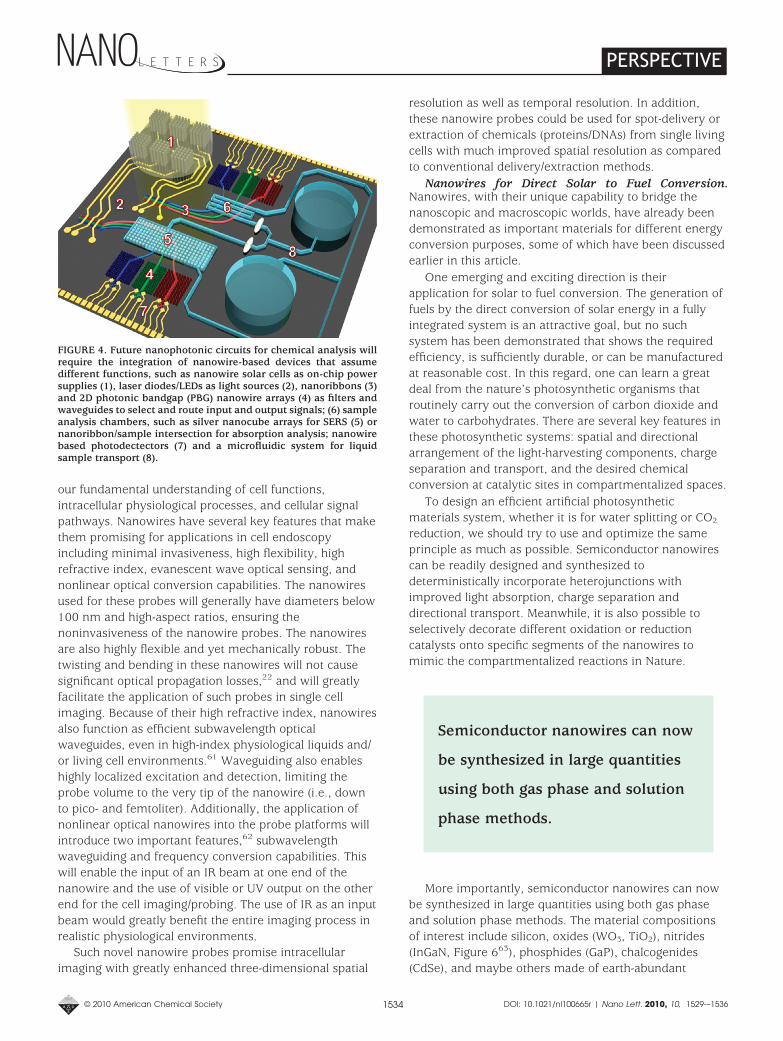
our fundamental understanding of cell functions,intracellular physiological processes, and cellular signalpathways. Nanowires have several key features that makethem promising for applications in cell endoscopyincluding minimal invasiveness, high flexibility, highrefractive index, evanescent wave optical sensing, andnonlinear optical conversion capabilities. The nanowiresused for these probes will generally have diameters below100 nm and high-aspect ratios, ensuring thenoninvasiveness of the nanowire probes. The nanowiresare also highly flexible and yet mechanically robust. Thetwisting and bending in these nanowires will not causesignificant optical propagation losses,22 and will greatlyfacilitate the application of such probes in single cellimaging. Because of their high refractive index, nanowiresalso function as efficient subwavelength opticalwaveguides, even in high-index physiological liquids and/or living cell environments.61 Waveguiding also enableshighly localized excitation and detection, limiting theprobe volume to the very tip of the nanowire (i.e., downto pico- and femtoliter). Additionally, the application ofnonlinear optical nanowires into the probe platforms willintroduce two important features,62 subwavelengthwaveguiding and frequency conversion capabilities. Thiswill enable the input of an IR beam at one end of thenanowire and the use of visible or UV output on the otherend for the cell imaging/probing. The use of IR as an inputbeam would greatly benefit the entire imaging process inrealistic physiological environments.
Such novel nanowire probes promise intracellularimaging with greatly enhanced three-dimensional spatial
resolution as well as temporal resolution. In addition,these nanowire probes could be used for spot-delivery orextraction of chemicals (proteins/DNAs) from single livingcells with much improved spatial resolution as comparedto conventional delivery/extraction methods.
Nanowires for Direct Solar to Fuel Conversion.Nanowires, with their unique capability to bridge thenanoscopic and macroscopic worlds, have already beendemonstrated as important materials for different energyconversion purposes, some of which have been discussedearlier in this article.
One emerging and exciting direction is theirapplication for solar to fuel conversion. The generation offuels by the direct conversion of solar energy in a fullyintegrated system is an attractive goal, but no suchsystem has been demonstrated that shows the requiredefficiency, is sufficiently durable, or can be manufacturedat reasonable cost. In this regard, one can learn a greatdeal from the nature’s photosynthetic organisms thatroutinely carry out the conversion of carbon dioxide andwater to carbohydrates. There are several key features inthese photosynthetic systems: spatial and directionalarrangement of the light-harvesting components, chargeseparation and transport, and the desired chemicalconversion at catalytic sites in compartmentalized spaces.
To design an efficient artificial photosyntheticmaterials system, whether it is for water splitting or CO2
reduction, we should try to use and optimize the sameprinciple as much as possible. Semiconductor nanowirescan be readily designed and synthesized todeterministically incorporate heterojunctions withimproved light absorption, charge separation anddirectional transport. Meanwhile, it is also possible toselectively decorate different oxidation or reductioncatalysts onto specific segments of the nanowires tomimic the compartmentalized reactions in Nature.
More importantly, semiconductor nanowires can nowbe synthesized in large quantities using both gas phaseand solution phase methods. The material compositionsof interest include silicon, oxides (WO3, TiO2), nitrides(InGaN, Figure 663), phosphides (GaP), chalcogenides(CdSe), and maybe others made of earth-abundant
FIGURE 4. Future nanophotonic circuits for chemical analysis willrequire the integration of nanowire-based devices that assumedifferent functions, such as nanowire solar cells as on-chip powersupplies (1), laser diodes/LEDs as light sources (2), nanoribbons (3)and 2D photonic bandgap (PBG) nanowire arrays (4) as filters andwaveguides to select and route input and output signals; (6) sampleanalysis chambers, such as silver nanocube arrays for SERS (5) ornanoribbon/sample intersection for absorption analysis; nanowirebased photodectectors (7) and a microfluidic system for liquidsample transport (8).
Semiconductor nanowires can now
be synthesized in large quantities
using both gas phase and solution
phase methods.
PERSPECTIVE
© 2010 American Chemical Society 1534 DOI: 10.1021/nl100665r | Nano Lett. 2010, 10, 1529-–1536
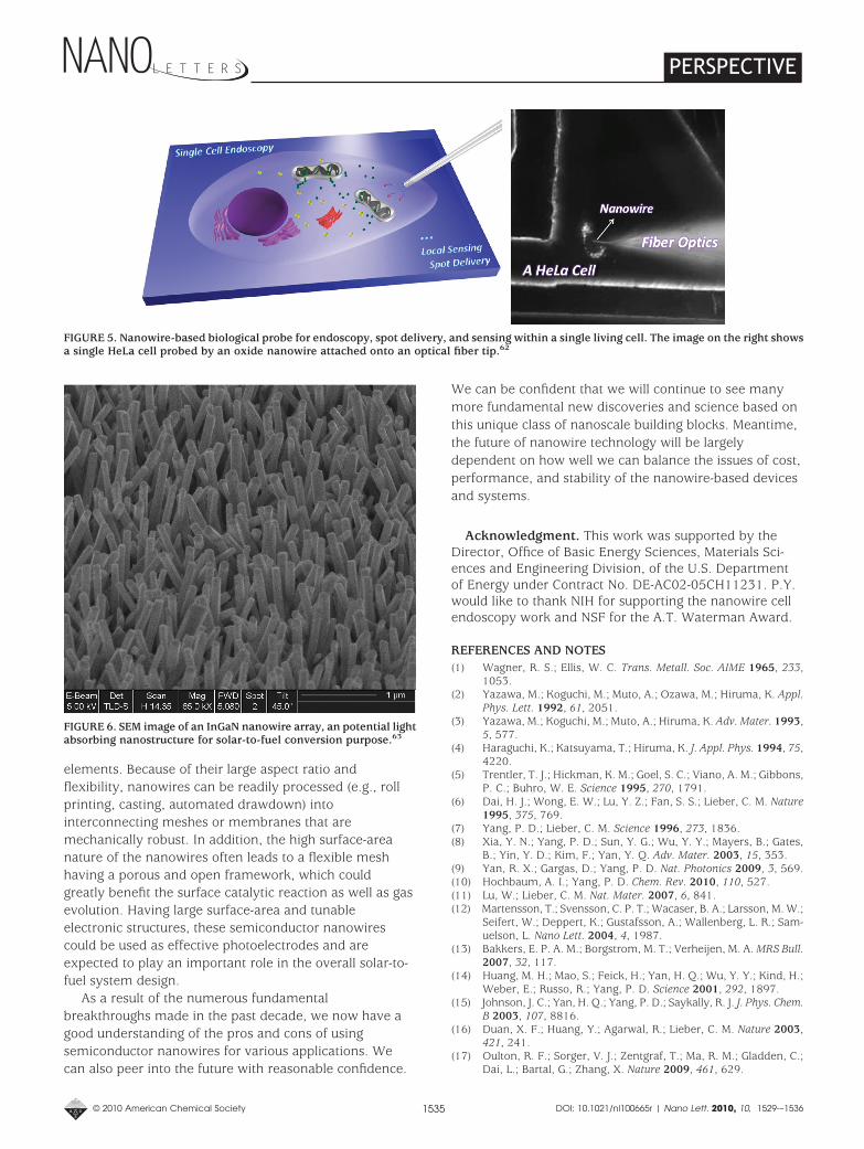
elements. Because of their large aspect ratio andflexibility, nanowires can be readily processed (e.g., rollprinting, casting, automated drawdown) intointerconnecting meshes or membranes that aremechanically robust. In addition, the high surface-areanature of the nanowires often leads to a flexible meshhaving a porous and open framework, which couldgreatly benefit the surface catalytic reaction as well as gasevolution. Having large surface-area and tunableelectronic structures, these semiconductor nanowirescould be used as effective photoelectrodes and areexpected to play an important role in the overall solar-to-fuel system design.
As a result of the numerous fundamentalbreakthroughs made in the past decade, we now have agood understanding of the pros and cons of usingsemiconductor nanowires for various applications. Wecan also peer into the future with reasonable confidence.
We can be confident that we will continue to see manymore fundamental new discoveries and science based onthis unique class of nanoscale building blocks. Meantime,the future of nanowire technology will be largelydependent on how well we can balance the issues of cost,performance, and stability of the nanowire-based devicesand systems.
Acknowledgment. This work was supported by theDirector, Office of Basic Energy Sciences, Materials Sci-ences and Engineering Division, of the U.S. Departmentof Energy under Contract No. DE-AC02-05CH11231. P.Y.would like to thank NIH for supporting the nanowire cellendoscopy work and NSF for the A.T. Waterman Award.
REFERENCES AND NOTES(1) Wagner, R. S.; Ellis, W. C. Trans. Metall. Soc. AIME 1965, 233,
1053.(2) Yazawa, M.; Koguchi, M.; Muto, A.; Ozawa, M.; Hiruma, K. Appl.
Phys. Lett. 1992, 61, 2051.(3) Yazawa, M.; Koguchi, M.; Muto, A.; Hiruma, K. Adv. Mater. 1993,
5, 577.(4) Haraguchi, K.; Katsuyama, T.; Hiruma, K. J. Appl. Phys. 1994, 75,
4220.(5) Trentler, T. J.; Hickman, K. M.; Goel, S. C.; Viano, A. M.; Gibbons,
P. C.; Buhro, W. E. Science 1995, 270, 1791.(6) Dai, H. J.; Wong, E. W.; Lu, Y. Z.; Fan, S. S.; Lieber, C. M. Nature
1995, 375, 769.(7) Yang, P. D.; Lieber, C. M. Science 1996, 273, 1836.(8) Xia, Y. N.; Yang, P. D.; Sun, Y. G.; Wu, Y. Y.; Mayers, B.; Gates,
B.; Yin, Y. D.; Kim, F.; Yan, Y. Q. Adv. Mater. 2003, 15, 353.(9) Yan, R. X.; Gargas, D.; Yang, P. D. Nat. Photonics 2009, 3, 569.(10) Hochbaum, A. I.; Yang, P. D. Chem. Rev. 2010, 110, 527.(11) Lu, W.; Lieber, C. M. Nat. Mater. 2007, 6, 841.(12) Martensson, T.; Svensson, C. P. T.; Wacaser, B. A.; Larsson, M. W.;
Seifert, W.; Deppert, K.; Gustafsson, A.; Wallenberg, L. R.; Sam-uelson, L. Nano Lett. 2004, 4, 1987.
(13) Bakkers, E. P. A. M.; Borgstrom, M. T.; Verheijen, M. A. MRS Bull.2007, 32, 117.
(14) Huang, M. H.; Mao, S.; Feick, H.; Yan, H. Q.; Wu, Y. Y.; Kind, H.;Weber, E.; Russo, R.; Yang, P. D. Science 2001, 292, 1897.
(15) Johnson, J. C.; Yan, H. Q.; Yang, P. D.; Saykally, R. J. J. Phys. Chem.B 2003, 107, 8816.
(16) Duan, X. F.; Huang, Y.; Agarwal, R.; Lieber, C. M. Nature 2003,421, 241.
(17) Oulton, R. F.; Sorger, V. J.; Zentgraf, T.; Ma, R. M.; Gladden, C.;Dai, L.; Bartal, G.; Zhang, X. Nature 2009, 461, 629.
FIGURE 5. Nanowire-based biological probe for endoscopy, spot delivery, and sensing within a single living cell. The image on the right showsa single HeLa cell probed by an oxide nanowire attached onto an optical fiber tip.62
FIGURE 6. SEM image of an InGaN nanowire array, an potential lightabsorbing nanostructure for solar-to-fuel conversion purpose.63
PERSPECTIVE
© 2010 American Chemical Society 1535 DOI: 10.1021/nl100665r | Nano Lett. 2010, 10, 1529-–1536
(18) Hill, M. T.; Oei, Y. S.; Smalbrugge, B.; Zhu, Y.; De Vries, T.; VanVeldhoven, P. J.; Van Otten, F. W. M.; Eijkemans, T. J.; Turkiewicz,J. P.; De Waardt, H.; Geluk, E. J.; Kwon, S. H.; Lee, Y. H.; Notzel,R.; Smit, M. K. Nat. Photonics 2007, 1, 589.
(19) Li, D. Y.; Wu, Y. Y.; Kim, P.; Shi, L.; Yang, P. D.; Majumdar, A.Appl. Phys. Lett. 2003, 83, 2934.
(20) Hochbaum, A. I.; Chen, R. K.; Delgado, R. D.; Liang, W. J.; Garnett,E. C.; Najarian, M.; Majumdar, A.; Yang, P. D. Nature 2008, 451,163.
(21) Li, Y.; Qian, F.; Xiang, J.; Lieber, C. M. Mater. Today. 2006, 9, 18.(22) Law, M.; Sirbuly, D. J.; Johnson, J. C.; Goldberger, J.; Saykally, R. J.;
Yang, P. D. Science 2004, 305, 1269.(23) Yan, R. X.; Pausauskie, P.; Huang, J. X.; Yang, P. D. Proc. Natl.
Acad. Sci. U.S.A. 2009, 106, 21045.(24) Kim, W.; Ng, J. K.; Kunitake, M. E.; Conklin, B. R.; Yang, P. D.
J. Am. Chem. Soc. 2007, 129, 7228.(25) Hallstrom, W.; Martensson, T.; Prinz, C.; Gustavsson, P.; Mon-
telius, L.; Samuelson, L.; Kanje, M. Nano Lett. 2007, 7, 2960.(26) Shalek, A. K.; Robinson, J. T.; Karp, E. S.; Lee, J. S.; Ahn, D. R.;
Yoon, M. H.; Sutton, A.; Jorgolli, M.; Gertner, R. S.; Gujral, T. S.;MacBeath, G.; Yang, E. G.; Park, H. Proc. Natl. Acad. Sci. U.S.A.2010, 107, 1870.
(27) Patolsky, F.; Timko, B. P.; Yu, G. H.; Fang, Y.; Greytak, A. B.;Zheng, G. F.; Lieber, C. M. Science 2006, 313, 1100.
(28) Ponce, F. A.; Bour, D. P. Nature 1997, 386, 351.(29) Duan, X. F.; Huang, Y.; Cui, Y.; Wang, J. F.; Lieber, C. M. Nature
2001, 409, 66.(30) Huang, Y.; Duan, X. F.; Lieber, C. M. Small 2005, 1, 142.(31) Zhong, Z. H.; Qian, F.; Wang, D. L.; Lieber, C. M. Nano Lett. 2003,
3, 343.(32) Minot, E. D.; Kelkensberg, F.; van Kouwen, M.; van Dam, J. A.;
Kouwenhoven, L. P.; Zwiller, V.; Borgstrom, M. T.; Wunnicke, O.;Verheijen, M. A.; Bakkers, E. P. A. M. Nano Lett. 2007, 7, 367.
(33) Qian, F.; Li, Y.; Gradecak, S.; Wang, D. L.; Barrelet, C. J.; Lieber,C. M. Nano Lett. 2004, 4, 1975.
(34) Mukai, T. IEEE J. Sel. Top. Quantum Electron. 2002, 8, 264.(35) Law, M.; Greene, L. E.; Johnson, J. C.; Saykally, R.; Yang, P. D.
Nat. Mater. 2005, 4, 455.(36) Law, M.; Greene, L. E.; Radenovic, A.; Kuykendall, T.; Liphardt,
J.; Yang, P. D. J. Phys. Chem. B 2006, 110, 22652.(37) Tian, B. Z.; Zheng, X. L.; Kempa, T. J.; Fang, Y.; Yu, N. F.; Yu,
G. H.; Huang, J. L.; Lieber, C. M. Nature 2007, 449, 885.(38) Garnett, E.; Yang, P. Nano. Lett., in press.(39) Green, M. A. Physica E 2002, 14, 65.(40) Wang, Z. L.; Song, J. H. Science 2006, 312, 242.
(41) Wang, X. D.; Song, J. H.; Liu, J.; Wang, Z. L. Science 2007, 316,102.
(42) Qin, Y.; Wang, X. D.; Wang, Z. L. Nature 2008, 451, 809.(43) Xu, S.; Wei, Y. G.; Liu, J.; Yang, R.; Wang, Z. L. Nano Lett. 2008,
8, 4027.(44) Yang, R. S.; Qin, Y.; Dai, L. M.; Wang, Z. L. Nat. Nanotechnol. 2009,
4, 34.(45) Wang, X. D.; Liu, J.; Song, J. H.; Wang, Z. L. Nano Lett. 2007, 7,
2475.(46) Yang, R.; Qin, Y.; Li, C.; Zhu, G.; Wang, Z. L. Nano Lett. 2009, 9,
1201.(47) Liu, J.; Fei, P.; Zhou, J.; Tummala, R.; Wang, Z. L. Appl. Phys. Lett.
2008, 92.(48) Wang, Z. L. Adv. Funct. Mater. 2008, 18, 3553.(49) Lu, M. P.; Song, J.; Lu, M. Y.; Chen, M. T.; Gao, Y.; Chen, L. J.;
Wang, Z. L. Nano Lett. 2009, 9, 1223.(50) Howells, C. A. Energy Convers. Manage. 2009, 50, 1847.(51) Zhong Lin, W.; Xudong, W.; Jinhui, S.; Jin, L.; Yifan, G. IEEE
Pervasive Comput. 2008, 7, 49.(52) Boukai, A. I.; Bunimovich, Y.; Tahir-Kheli, J.; Yu, J. K.; Goddard,
W. A.; Heath, J. R. Nature 2008, 451, 168.(53) Cui, Y.; Wei, Q. Q.; Park, H. K.; Lieber, C. M. Science 2001, 293,
1289.(54) Zheng, G. F.; Patolsky, F.; Cui, Y.; Wang, W. U.; Lieber, C. M. Nat.
Biotechnol. 2005, 23, 1294.(55) Hu, Y. J.; Churchill, H. O. H.; Reilly, D. J.; Xiang, J.; Lieber, C. M.;
Marcus, C. M. Nat. Nanotechnol. 2007, 2, 622.(56) Pauzauskie, P. J.; Sirbuly, D. J.; Yang, P. D. Phys. Rev. Lett. 2006,
96, 143903.(57) Johnson, J. C.; Choi, H. J.; Knutsen, K. P.; Schaller, R. D.; Yang,
P. D.; Saykally, R. J. Nat. Mater. 2002, 1, 106.(58) Stern, E.; Klemic, J. F.; Routenberg, D. A.; Wyrembak, P. N.;
Turner-Evans, D. B.; Hamilton, A. D.; LaVan, D. A.; Fahmy, T. M.;Reed, M. A. Nature 2007, 445, 519.
(59) Melosh, N. A.; Boukai, A.; Diana, F.; Gerardot, B.; Badolato, A.;Petroff, P. M.; Heath, J. R. Science 2003, 300, 112.
(60) Beckman, R.; Johnston-Halperin, E.; Luo, Y.; Green, J. E.; Heath,J. R. Science 2005, 310, 465.
(61) Sirbuly, D. J.; Law, M.; Pauzauskie, P.; Yan, H. Q.; Maslov, A. V.;Knutsen, K.; Ning, C. Z.; Saykally, R. J.; Yang, P. D. Proc. Natl.Acad. Sci. U.S.A. 2005, 102, 7800.
(62) Nakayama, Y.; Pauzauskie, P. J.; Radenovic, A.; Onorato, R. M.;Saykally, R. J.; Liphardt, J.; Yang, P. D. Nature 2007, 447, 1908.
(63) Kuykendall, T.; Ulrich, P.; Aloni, S.; Yang, P. Nat. Mater. 2007, 6,951.
PERSPECTIVE
© 2010 American Chemical Society 1536 DOI: 10.1021/nl100665r | Nano Lett. 2010, 10, 1529-–1536

![119 Nanowires 4. Nanowires - UFAMhome.ufam.edu.br/berti/nanomateriais/Nanowires.pdf · 119 Nanowires 4. Nanowires ... written about carbon nanotubes [4.57–59], which can be ...](https://static.fdocuments.net/doc/165x107/5abfd11e7f8b9a5d718eba2b/119-nanowires-4-nanowires-nanowires-4-nanowires-written-about-carbon-nanotubes.jpg)