
Fully Integrated CMOS Transmitter and Power Amplifier for ...
34
Fully Integrated CMOS Transmitter and Power Amplifier for Software Defined Radios and Cognitive Radios Immanuel Raja and Gaurab Banerjee, Department of Electrical Communication Engineering, Indian Institute of Science, Bangalore, INDIA Problem Statement The aim of this thesis is to design a complete transmitter with an integrated power amplifier in CMOS that can serve as an RF front- end for software defined radios. The requirements are: ➢ Reconfigurability -- to transmit at different carrier frequencies and maintain sufficient output power and efficiency across the entire frequency range. ➢ Transmit signals with different modulation schemes -- both constant and varying envelope signals. ➢ Transmit signals with different bandwidths. ➢ Output power control at all frequencies. Advantages ➢ Tunability required only at the output stage. ➢ Reconfiguration of baseband digital filters is much easier to accomplish. ➢ Scales well with technology. Output Power Drain Efficiency Suppression of the 2 nd harmonic spur Output power and efficiency vs input code Predistortion to linearize the DAC. Proposed Transmitter Architecture ➢ Digital inputs – I and Q data streams (9-bits wide each) ➢ RF Input – Continuous wave signal at 2 x f C ➢ Clock generation block – generates differential rail-to-rail quadrature clock phases. ➢ Digital processing block – DPD, 2 levels of filtering. ➢ Digital mixing ➢ Tunable RF Power DAC as the output stage. Website: http://www.ece.iisc.ernet.in/~arsl E-Mail: [email protected] Figure: Modifying a traditional transmitter for SDR. Figure: Proposed transmitter architecture. Figure: Digital signal processing for spur suppression. Figure: RF-DAC PA Switches. Figure: Reconfigurable Class-E PA Schematic. Frequency 800 MHz 1 GHz 2 GHz EVM (RMS) 3.1% 4% 13.4% Magnitude Error 1.6% 1.9% 8.3% Phase Error 2.15 deg 3.5 deg 10.4 deg Quadrature Error 0.7 deg 1.1 deg 3.6 deg Gain Imbalance 0.3 dB 0.3 dB 0.14 dB Measured linearity parameters while transmitting a 16 QAM signal at different carrier frequencies. Publications I. Raja and G. Banerjee, “An inductor-less transmission line based 60 GHz PA in 65-nm CMOS with analog power control,” IEEE ICECS, Monte Carlo, 2016, pp. 149-152. I. Raja, V. Khatri, Z. Zahir and G. Banerjee, “A 0.1–2-GHz Quadrature Correction Loop for Digital Multiphase Clock Generation Circuits in 130-nm CMOS,” in IEEE TVLSI Systems, vol. 25, no. 3, pp. 1044-1053, March 2017. I. Raja, G. Banerjee, M. A. Zeidan and J. A. Abraham, “A 0.1–3.5-GHz Duty-Cycle Measurement and Correction Technique in 130-nm CMOS,” in IEEE TVLSI Systems, vol. 24, no. 5, pp. 1975-1983, May 2016. J. S. Gaggatur, V. Khatri, I. Raja, M. K. Lenka and G. Banerjee, “Differential multi-phase DLL for reconfigurable radio frequency synthesizer,” 2014 IEEE CONECCT, Bangalore, 2014, pp. 1-5.
Transcript of Fully Integrated CMOS Transmitter and Power Amplifier for ...

Fully Integrated CMOS Transmitter and Power Amplifier for
Software Defined Radios and Cognitive RadiosImmanuel Raja and Gaurab Banerjee, Department of Electrical Communication Engineering,
Indian Institute of Science, Bangalore, INDIA
Problem StatementThe aim of this thesis is to design a complete transmitter with an integrated power amplifier in CMOS that can serve as an RF front-end for software defined radios. The requirements are:Reconfigurability -- to transmit at different carrier frequencies and maintain sufficient output power and efficiency across the entire frequency range.
Transmit signals with different modulation schemes -- both constant and varying envelope signals.
Transmit signals with different bandwidths.Output power control at all frequencies.
AdvantagesTunability required only at the output stage.
Reconfiguration of baseband digital filters is much easier to accomplish.
Scales well with technology.
Output Power Drain Efficiency Suppression of the 2nd harmonic spur Output power and efficiency vs input code
Predistortion to linearize the DAC.
Proposed Transmitter ArchitectureDigital inputs – I and Q data streams (9-bits wide each)RF Input – Continuous wave signal at 2 x fC
Clock generation block – generates differential rail-to-rail quadrature clock phases.
Digital processing block – DPD, 2 levels of filtering. Digital mixingTunable RF Power DAC as the output stage.
Website: http://www.ece.iisc.ernet.in/~arslE-Mail: [email protected]
Figure: Modifying a traditional transmitter for SDR.
Figure: Proposed transmitter architecture.
Figure: Digital signal processing for spur suppression.
Figure: RF-DAC PA Switches.
Figure: Reconfigurable Class-E PA Schematic.
Frequency 800 MHz 1 GHz 2 GHz
EVM(RMS)
3.1% 4% 13.4%
MagnitudeError
1.6% 1.9% 8.3%
Phase Error
2.15 deg 3.5 deg 10.4 deg
QuadratureError
0.7 deg 1.1 deg 3.6 deg
Gain Imbalance
0.3 dB 0.3 dB 0.14 dB
Measured linearity parameters while transmittinga 16 QAM signal at different carrier frequencies.
PublicationsI. Raja and G. Banerjee, “An inductor-less transmission line based 60 GHz PA in 65-nm CMOS with analog power control,” IEEE ICECS, Monte Carlo, 2016, pp. 149-152.I. Raja, V. Khatri, Z. Zahir and G. Banerjee, “A 0.1–2-GHz Quadrature Correction Loop for Digital Multiphase Clock Generation Circuits in 130-nm CMOS,” in IEEE TVLSI Systems, vol. 25, no. 3, pp. 1044-1053, March 2017.I. Raja, G. Banerjee, M. A. Zeidan and J. A. Abraham, “A 0.1–3.5-GHz Duty-Cycle Measurement and Correction Technique in 130-nm CMOS,” in IEEE TVLSI Systems, vol. 24, no. 5, pp. 1975-1983, May 2016.J. S. Gaggatur, V. Khatri, I. Raja, M. K. Lenka and G. Banerjee, “Differential multi-phase DLL for reconfigurable radio frequency synthesizer,” 2014 IEEE CONECCT, Bangalore, 2014, pp. 1-5.

Fully Integrated CMOS Transmitter and Power Amplifier
for Software Defined Radios and Cognitive Radios
Immanuel Raja
Under the guidance of
Dr. Gaurab Banerjee
Analog and RF Systems LaboratoryDepartment of Electrical Communication Engineering
Indian Institute of ScienceBangalore
Immanuel Raja (IISc) Fully Integrated CMOS TX for SDR 1 / 33

Overview
1 Introduction
2 Proposed Transmitter Architecture
3 Reconfigurable Power Amplifier
4 Conclusion
Immanuel Raja (IISc) Fully Integrated CMOS TX for SDR 2 / 33

Introduction – Software Defined Radio (SDR)
SDR is “a radio that is substantially defined in software and whosephysical layer behaviour can be significantly altered through changes to itssoftware... In other words, the same piece of hardware can be modified toperform different functions at different times, allowing the hardware to bespecifically tailored to the application in hand.”J. H. Reed, Software radio: a modern approach to radio engineering. Prentice Hall
Professional, 2002.
Benefits of SDR:
Multifunctionality
Ease of upgradation
Obsolescence mitigation
Global usage.
Figure : Block diagram of an ideal SDRtransceiver.
Immanuel Raja (IISc) Fully Integrated CMOS TX for SDR 3 / 33

Problem Statement
The aim of this thesis is to design a complete transmitter with an
integrated power amplifier in CMOS that can serve as an RF
front-end for software defined radios.
The requirements are:
Reconfigurability – to transmit at different carrier frequencies andmaintain sufficient output power and efficiency across the entirefrequency range.
Transmit signals with different modulation schemes – both constantand varying envelope signals.
Transmit signals with different bandwidths.
Output power control at all frequencies.
Immanuel Raja (IISc) Fully Integrated CMOS TX for SDR 4 / 33

Power Amplifier - Classes
Figure : Voltage and current waveformsfor different PA classes.
The Power Amplifier (PA) is at theheart of any transmitter. Thearchitectural design of thetransmitter heavily depends on thetype of PA used.
Linear PAs–Classes A, B, AB, CGood linearity with poorefficiency. Linearity traded offfor efficiency.
Switching PAs–Classes D, E, F,SHigh Efficiency, but can supportonly constant envelope signals.
Immanuel Raja (IISc) Fully Integrated CMOS TX for SDR 5 / 33

Modifying a Traditional Transmitter for SDR
Figure : Traditional transmitter architecture adapted for wideband SDR/CR
Extremely difficult to implement.
Tuning one block would affect the other blocks.
Digital transmitters are better suited for SDR applications.
Immanuel Raja (IISc) Fully Integrated CMOS TX for SDR 6 / 33

Techniques to use Switching PAs to Transmit Signals with
Amplitude Modulation
Immanuel Raja (IISc) Fully Integrated CMOS TX for SDR 7 / 33

Proposed Architecture
Figure : Detailed system diagram of theproposed transmitter
Digital inputs – I andQ data streams (9-bitswide each)
RF Input – Continuouswave signal at 2 × fc .
Clock generation block– generates differentialrail-to-rail quadratureclock phases.
Digital processingblock – DPD, 2 levelsof filtering.
Digital mixing
Tunable RF PowerDAC as the outputstage.
Immanuel Raja (IISc) Fully Integrated CMOS TX for SDR 8 / 33

Proposed Digital Filtering
Figure : Digital processing of the input signal for spur suppression
2 stages of up-sampling with filtering
Immanuel Raja (IISc) Fully Integrated CMOS TX for SDR 9 / 33

Measured Result – Transmitting a 16 QAM Signal
Figure : Wideband spectrum while transmitting at 1 GHz. The spurs exist only atthe harmonics of 1 GHz. The other spurs are cleaned up by the digital processingblock.
Immanuel Raja (IISc) Fully Integrated CMOS TX for SDR 10 / 33

Clock Generation
Figure : Quadrature clock generation and correction scheme. DCC: Duty CycleCorrector. QCC: Quadrature Correction Circuit
The input CW signal at 2 × fc is converted to differential rail-to-railquadrature signals.Duty cycle and quadrature impairments arise due to mismatches and PVTvariations – need real-time correctionAssorter to identify the I phase, Q phase and their complements.2 DCC circuits correct the I and Q phases to have 50% duty cycle.QCC corrects the quadrature error.DCC and QCC need to function across the entire frequency range – requirewide frequency range DCC and QCC circuits.
Immanuel Raja (IISc) Fully Integrated CMOS TX for SDR 11 / 33

Duty Cycle Correction
Figure : Architecture of the Duty CycleCorrector
Analog negative feedback loopto correct duty cycle errrors.
Duty cycle detector (DCD) –operates on differential clockphases – DC average.
Pulsewidth Modification Cell(PMC) – changes the duty cycleaccording to the control voltage.
Differential Amplifier – for gainand biasing the control voltage.
“A 0.13.5-GHz Duty-Cycle Measurement and Correction Technique in 130-nm CMOS,”in IEEE Transactions on Very Large Scale Integration (VLSI) Systems, vol. 24, no. 5,pp. 1975-1983, May 2016.
Immanuel Raja (IISc) Fully Integrated CMOS TX for SDR 12 / 33

Quadrature Correction Circuit
Figure : Architecture of the quadrature correction loop.
Fixed delay in the I path and a variable delay in the Q path.Quadrature error converted to duty cycle error using an XOR.Perfect quadrature implies 50% duty cycle at the XOR outputAnalog negative feedback loop which adjusts the delay on the Q pathto optimize for 50% duty cycle at the output of the XOR.
“A 0.1 to 2 GHz Quadrature Correction Loop for Digital Multiphase Clock GenerationCircuits in 130-nm CMOS”, IEEE Transactions on Very Large Scale Integration (VLSI)Systems, vol. 25, no. 3, pp. 1044-1053, March 2017.
Immanuel Raja (IISc) Fully Integrated CMOS TX for SDR 13 / 33

Digital Mixing
I+
I-
SGN_I
BI0
BI7
Q+
Q-
SGN_Q
BQ0
BQ7
8
8
0
1
0
1
PA
Class-E
Reconfigurable
Figure : Schematic of the mixer and drivers
Mixing using NAND gates.
25% duty-cycle clocks used to obtain effective 50% ON/OFF time atthe PA.
Complementary phase selected for negative data values.
Immanuel Raja (IISc) Fully Integrated CMOS TX for SDR 14 / 33

Reconfigurable Class-E Power Amplifier
Design
“A 0.75 2.5 GHz All-Digital RF Transmitter with a Tunable IntegratedClass-E Power Amplifier for SDR/CR” Immanuel Raja, Gaurab Banerjee.
(Manuscript under preparation.)
Immanuel Raja (IISc) Fully Integrated CMOS TX for SDR 15 / 33

Traditional Class-E Implementation
Vdd
LDC
L0 C0 X
CSH
SWITCH
RL
tuned at ω0
Figure : Traditional Class-E poweramplifier schematic.
Vdd
LS
R0=50ΩCPCSH
LDC
SWITCH
CDC
Figure : Implementation of a Class-Epower amplifier showing the impedancetransformation network.
RL = 0.5768V 2
DD
POUT
CSH = 0.18361
ωRL
X = 1.152RL
ZL =R0
1 + (ωR0CP )2+ j
(
ωLS −ωR2
0CP
1 + (ωR0CP)2
)
The component values are calculated as follows:
CP =1
ωR0
√
R0
RL
− 1
LS =1
ω
(
X +ωR2
0CP
1 + (ωR0CP)2
)
Immanuel Raja (IISc) Fully Integrated CMOS TX for SDR 16 / 33

Component Values for a Traditional Class-E PA
POUT = 18 dBm RL = 18Ω VDD = 1.5 V
Frequency CP LS CSH
750 MHz 5.08 pF 10.25 nH 1.89 pF
800 MHz 4.76 pF 9.6 nH 1.77 pF
1 GHz 3.8 pF 7.68 nH 1.42 pF
1.5 GHz 2.54 pF 5.12 nH 947 fF
2 GHz 1.9 pF 3.84 nH 710 fF
2.5 GHz 1.52 pF 3.07 nH 568 fF
LS varies from 3nH to 10.25nH which is impossible to synthesizeon-chip.
Using a varactor tuned secondary to change the effective inductanceof the primary in a transformer – very less inductance range.
Need to design Class-E PAs with a fixed LS over a wide frequencyrange.
Immanuel Raja (IISc) Fully Integrated CMOS TX for SDR 17 / 33
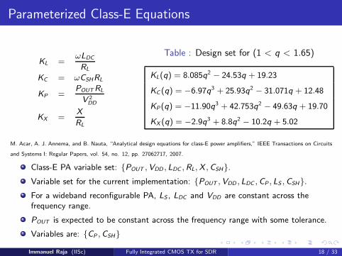
Parameterized Class-E Equations
KL =ωLDC
RL
KC = ωCSHRL
KP =POUTRL
V 2DD
KX =X
RL
Table : Design set for (1 < q < 1.65)
KL(q) = 8.085q2 − 24.53q + 19.23
KC (q) = −6.97q3 + 25.93q2 − 31.071q + 12.48
KP(q) = −11.90q3 + 42.753q2 − 49.63q + 19.70
KX (q) = −2.9q3 + 8.8q2 − 10.2q + 5.02
M. Acar, A. J. Annema, and B. Nauta, “Analytical design equations for class-E power amplifiers,” IEEE Transactions on Circuits
and Systems I: Regular Papers, vol. 54, no. 12, pp. 27062717, 2007.
Class-E PA variable set: POUT ,VDD , LDC ,RL,X ,CSH.
Variable set for the current implementation: POUT ,VDD , LDC ,CP , LS ,CSH.
For a wideband reconfigurable PA, LS , LDC and VDD are constant across thefrequency range.
POUT is expected to be constant across the frequency range with some tolerance.
Variables are: CP ,CSH
Immanuel Raja (IISc) Fully Integrated CMOS TX for SDR 18 / 33

Digital-to-RF Conversion – RF-DAC
Vprot
... ...
Vdd
I Path Q Path
Thick-oxide devices
BI0 BI1 BI7 BQ0 BQ1 BQ7
LDC
Binary-weighted switches form the switch of the PA.
25% duty cycle for I and Q paths such that the maximum ON period of thetotal switch is 50%.
Binary-weighted thick oxide devices for protecting the switching transistors.
Vprot chosen such that resistance of the thick oxide transistor is minimizedand bottom device is protected at the same time.
Immanuel Raja (IISc) Fully Integrated CMOS TX for SDR 19 / 33
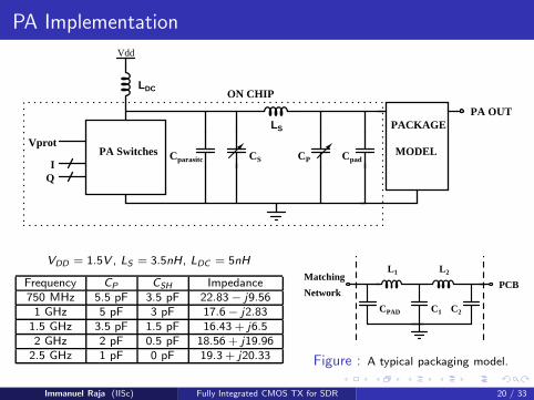
PA Implementation
Vdd
PA SwitchesVprot
IQ
Cparasitc CP CpadCS
PA OUT
ON CHIP
PACKAGE LS
LDC
MODEL
VDD = 1.5V , LS = 3.5nH, LDC = 5nH
Frequency CP CSH Impedance750 MHz 5.5 pF 3.5 pF 22.83− j9.561 GHz 5 pF 3 pF 17.6− j2.831.5 GHz 3.5 pF 1.5 pF 16.43 + j6.52 GHz 2 pF 0.5 pF 18.56 + j19.962.5 GHz 1 pF 0 pF 19.3 + j20.33
Matching
NetworkPCB
CPAD C2C1
L1 L2
Figure : A typical packaging model.
Immanuel Raja (IISc) Fully Integrated CMOS TX for SDR 20 / 33

Chip Details
Figure : Chip micrograph.
Fabricated in UMC 130nm RFCMOS process (8 metal layers).
Active area: 1mm × 1mm.
Packaged in a QFN48 .
Digital Pre-distortion (DPD), FIR filtering, DC feed inductor implemented off-chip.
Immanuel Raja (IISc) Fully Integrated CMOS TX for SDR 21 / 33

Experimental Setup for Test and Measurement
Immanuel Raja (IISc) Fully Integrated CMOS TX for SDR 22 / 33

Measured ResultsOutput Power
0.75 1 1.25 1.5 1.75 2 2.25 2.5
x 109
−10
−5
0
5
10
15
20
Frequency
Out
put P
ower
in d
Bm
Measured ouput powerSimulated output power
Efficiency
0.75 1 1.25 1.5 1.75 2 2.25 2.5
x 109
0
5
10
15
20
25
30
35
40
45
50
Frequency
Dra
in E
ffici
ency
in %
Measured efficiencySimulated efficiency
2nd harmonic suppression
0.75 1 1.25 1.5 1.75 2 2.25 2.5
x 109
0
5
10
15
20
25
30
35
40
Frequency
Sup
pres
sion
of 2
nd H
arm
onic
in d
Bc
Measured suppressionSimulated suppression
Reasons for discrepancies between simulated
and measured performance:
Inductor performance.
Off-chip placement of the DC Feedinductor.
High frequency slew degradation atpossibly slow corner, high temperatureoperation.
Immanuel Raja (IISc) Fully Integrated CMOS TX for SDR 23 / 33

Measured Results – DAC Performance and Digital
Pre-distortion (DPD)
0 50 100 150 200 250−25
−20
−15
−10
−5
0
5
10
15
Input Code
Out
put P
ower
in d
Bm
0 50 100 150 200 2500
2
4
6
8
10
12
14
16
Effi
cien
cy in
%
Output Power in dBmEfficiency
0 50 100 150 200 2500
0.1
0.2
0.3
0.4
0.5
0.6
0.7
0.8
0.9
1
Input CodeD
AC
Out
put V
olta
ge (
RM
S)
PA OutputIdeal DAC voltageAfter Pre−distortio
End-fit linearization for the DAC.
Mapping the equivalent voltage characteristics to a straight line.
Jumps at MSB transitions can be avoided by using thermometerencoding.
Immanuel Raja (IISc) Fully Integrated CMOS TX for SDR 24 / 33

Measured Results – Transmitting a 16 QAM Signal
Figure : Close-up spectrum while transmitting a 16-QAM signal at 1 GHz.
Frequency 800 MHz 1 GHz 2 GHzEVM(RMS)
3.1% 4% 13.4%
MagnitudeError
1.6% 1.9% 8.3%
Phase Er-ror
2.15 deg 3.5 deg 10.4 deg
QuadratureError
0.7 deg 1.1 deg 3.6 deg
Gain Im-balance
0.3 dB 0.3 dB 0.14 dB
Immanuel Raja (IISc) Fully Integrated CMOS TX for SDR 25 / 33

Comparison with the State-of-the-Art
Reference Yin2015 Ingels2010 This work
PA Class Class-AB Buffer Common SourcePre-power ampli-fier
Class E
Frequency Range 4-band solutionbetween 0.1 to6 GHz (0.1-0.7,0.7-1.4, 1.2-3.2,3-6) GHz
0.75 - 2.5 GHz 0.75 - 2.5 GHz
Output Power 2dBm 0-4 dBm 5-13 dBm
Efficiency – – 8-14%
EVM 2.3% @ 1.7dBm,LTE20 QPSK
3.2% @ 0dBm 4% for 16-QAMat 1 GHz withoutbackoff
Technology 65nm CMOS 40nm CMOS 130nm CMOS
VDD 2.5V 2.5V 1.5V
Area 2.2× 0.95mm2 1.3mm2 1mm2
Immanuel Raja (IISc) Fully Integrated CMOS TX for SDR 26 / 33

Conclusion
Immanuel Raja (IISc) Fully Integrated CMOS TX for SDR 27 / 33

Key Contributions
A fully integrated CMOS transmitter and power amplifierfor SDR has been designed and developed.The main contributions to the field as presented in this thesis are asfollows:
Differential quadrature clock generation across a wide frequencyrange from a single-ended CW input at twice the carrier frequency.
Architectural solutions for suppression of spurious components arisingdue of sampling of digital signals.
Duty cycle correction (DCC) circuit working across the entirefrequency range.
An alternate duty cycle measurement algorithm. Using frequencydomain information of the signal up to the third harmonic, timedomain information like duty cycle, rise and fall times can becalculated.
Immanuel Raja (IISc) Fully Integrated CMOS TX for SDR 28 / 33

Key Contributions (Contd.)
Quadrature correction circuit functional across the entire frequencyrange.
Development of theory and design methodology for a reconfigurableClass-E PA, with a single fixed series inductor. The PA is reconfiguredthrough capacitor banks.
Design of CMOS power amplifier that can span this wide frequencyrange with sufficient output power and efficiency, uniformly across thefrequency range, supporting varying envelope complex modulationsignals, with good linearity across the frequency range.
Digital power control over the frequency range of interest.
Digital pre-distortion scheme for the designed PA.
The proposed transmitter is the first reported wide-range all digital
RF transmitter with an integrated tunable Class-E PA which can
support non-constant envelope complex modulation.
Immanuel Raja (IISc) Fully Integrated CMOS TX for SDR 29 / 33

Publications
I. Raja; G. Banerjee; M. A. Zeidan; J. A. Abraham, “A 0.1-3.5-GHzDuty-Cycle Measurement and Correction Technique in 130-nmCMOS,” in IEEE Transactions on Very Large Scale Integration (VLSI)Systems , (Accepted/In press - Oct 8 2015 – Early Access)
I. Raja, V. Khatri, Z.Zaira, G. Banerjee, “A 0.1 to 2 GHz QuadratureCorrection Loop for Digital Multiphase Clock Generation Circuits in130-nm CMOS” Submitted to IEEE Transactions on Very Large ScaleIntegration (VLSI) Systems
I. Raja, G. Banerjee, “A 0.75 2.5 GHz All-Digital RF Transmitterwith a Tunable Integrated Class-E Power Amplifier for SDR/CR”(Manuscript under preparation.)
Immanuel Raja (IISc) Fully Integrated CMOS TX for SDR 30 / 33

Fabricated Chips
Immanuel Raja (IISc) Fully Integrated CMOS TX for SDR 31 / 33

Future Directions
Thermometer implementation of the DAC – to improve linearity andmonotonicity.
Better modelling of passives and interconnects.
Use of differential architecture to suppress the 2nd harmonic content.
Implementation in advanced technology nodes – lesser powerconsumption by digital blocks, clock and driver circuitry.
Implementation in advanced technology nodes – more stacking of thePA transistors – higher supply voltages – higher output power.
Immanuel Raja (IISc) Fully Integrated CMOS TX for SDR 32 / 33

Thank You
Immanuel Raja (IISc) Fully Integrated CMOS TX for SDR 33 / 33


![Operational Transconductance Amplifier (OTA) in 45nm CMOS · Amplifier (OTA) in 45nm CMOS YOUNGSEOK LEE ... Design of Analog CMOS Integrated Circuits. McGraw-Hill, 2002. [2] B. Ahuja,](https://static.fdocuments.net/doc/165x107/5fbfc7035b7a87264a188ff5/operational-transconductance-amplifier-ota-in-45nm-cmos-amplifier-ota-in-45nm.jpg)