Characterization of local dielectric breakdown in...
9
Characterization of local dielectric breakdown in ultrathin SiO 2 films using scanning tunneling microscopy and spectroscopy Heiji Watanabe, Toshio Baba, and Masakazu Ichikawa Citation: Journal of Applied Physics 85, 6704 (1999); doi: 10.1063/1.370182 View online: http://dx.doi.org/10.1063/1.370182 View Table of Contents: http://scitation.aip.org/content/aip/journal/jap/85/9?ver=pdfcov Published by the AIP Publishing Articles you may be interested in Electrical damage of an ultrathin Si oxynitride layer induced by scanning tunneling spectroscopy J. Appl. Phys. 92, 1850 (2002); 10.1063/1.1492865 Photo-enhanced negative differential resistance and photo-accelerated time-dependent dielectric breakdown in thin nitride-oxide dielectric film Appl. Phys. Lett. 78, 3241 (2001); 10.1063/1.1373409 Defect generation in ultrathin silicon dioxide films produced by anode hole injection Appl. Phys. Lett. 77, 2716 (2000); 10.1063/1.1320460 Scanning tunneling microscopy and spectroscopy characterization of ion-beam-induced dielectric degradation in ultrathin SiO 2 films and its thermal recovery process J. Appl. Phys. 87, 44 (2000); 10.1063/1.371824 Observation and creation of current leakage sites in ultrathin silicon dioxide films using scanning tunneling microscopy Appl. Phys. Lett. 72, 1987 (1998); 10.1063/1.121241 [This article is copyrighted as indicated in the article. Reuse of AIP content is subject to the terms at: http://scitation.aip.org/termsconditions. Downloaded to ] IP: 131.91.169.193 On: Mon, 24 Nov 2014 05:24:32
Transcript of Characterization of local dielectric breakdown in...

Characterization of local dielectric breakdown in ultrathin SiO 2 films using scanningtunneling microscopy and spectroscopyHeiji Watanabe, Toshio Baba, and Masakazu Ichikawa Citation: Journal of Applied Physics 85, 6704 (1999); doi: 10.1063/1.370182 View online: http://dx.doi.org/10.1063/1.370182 View Table of Contents: http://scitation.aip.org/content/aip/journal/jap/85/9?ver=pdfcov Published by the AIP Publishing Articles you may be interested in Electrical damage of an ultrathin Si oxynitride layer induced by scanning tunneling spectroscopy J. Appl. Phys. 92, 1850 (2002); 10.1063/1.1492865 Photo-enhanced negative differential resistance and photo-accelerated time-dependent dielectric breakdown inthin nitride-oxide dielectric film Appl. Phys. Lett. 78, 3241 (2001); 10.1063/1.1373409 Defect generation in ultrathin silicon dioxide films produced by anode hole injection Appl. Phys. Lett. 77, 2716 (2000); 10.1063/1.1320460 Scanning tunneling microscopy and spectroscopy characterization of ion-beam-induced dielectric degradation inultrathin SiO 2 films and its thermal recovery process J. Appl. Phys. 87, 44 (2000); 10.1063/1.371824 Observation and creation of current leakage sites in ultrathin silicon dioxide films using scanning tunnelingmicroscopy Appl. Phys. Lett. 72, 1987 (1998); 10.1063/1.121241
[This article is copyrighted as indicated in the article. Reuse of AIP content is subject to the terms at: http://scitation.aip.org/termsconditions. Downloaded to ] IP:
131.91.169.193 On: Mon, 24 Nov 2014 05:24:32
Characterization of local dielectric breakdown in ultrathin SiO 2 filmsusing scanning tunneling microscopy and spectroscopy
Heiji Watanabea) and Toshio BabaFundamental Research Laboratories, NEC Corporation, 34 Miyukigaoka, Tsukuba, Ibaraki 305-8501, Japan
Masakazu IchikawaJoint Research Center for Atom Technology, Angstrom Technology Partnership, 1-1-4 Higashi, Tsukuba,Ibaraki 305-0046, Japan
~Received 22 October 1998; accepted for publication 27 January 1999!
Local dielectric breakdown of ultrathin SiO2 films grown on silicon substrates has been investigatedby using scanning tunneling microscopy~STM! and scanning tunneling spectroscopy~STS!. Wefound that STM observation can reveal individual quasibreakdown spots created by hot-electroninjection into the oxide, as well as features of the topography such as atomic steps on the oxidesurface. STS was used to study the local electrical properties of the oxide films before and afterelectrical stressing. We observed a leakage current at the quasibreakdown spots that passed throughdefect levels in the ultrathin oxide films. We also found that several tunneling spectra obtained fromnear leakage sites showed clear negative differential resistance. This phenomenon was attributed tothe conductance change in the leakage path due to electron charging effects. Moreover, weconfirmed the stressing polarity dependence of the leakage-site creation, and that atomic steps on theoxide and at the SiO2/Si interface did not cause any serous problem in the quasibreakdown process.© 1999 American Institute of Physics.@S0021-8979~99!03709-3#
I. INTRODUCTION
Dielectric breakdown of SiO2 films continues to be atechnologically important issue concerning the operation ofmetal–oxide–semiconductor~MOS! devices. As individualdevices are scaled down, the gate-oxide thickness of MOSdevices will reach the nanometer level.1 When such ultrathinoxide films are used, quasibreakdown, as well as completebreakdown, has been observed after electrical stressing.2
These types of phenomena have been extensively studiedthrough the degradation characteristics of MOS capacitors,which provide spatially averaged information on the break-down processes. In the case of complete breakdown, micro-scopic analysis by cross-sectional transmission electron mi-croscope proved leakage sites to be physically damagedregions in the oxide films; these regions were composed ofcrystallized silicon that resulted from local Joule heating.3
On the other hand, the most likely quasibreakdown mecha-nism, as deduced from the characterization of MOS devicedegradation, has been reported to be trap-assisted tunnelingin ultrathin oxide films.2 In this process, hot-electron or hot-hole injection during electrical stressing is thought to createtrap levels in the oxide.4 However, due to technological dif-ficulties, there have been few reports on the microscopiccharacterization of the quasibreakdown, such as on the iden-tification of individual leakage sites or its local electricalproperties.
Recently, scanning probe techniques have been utilizedto study SiO2 films. The surface morphology of oxide filmshas been observed by using atomic force microscopy~AFM!,5–7 and a conductive cantilever has been used for
electrical analysis.8 Several groups have used ballistic elec-tron emission microscopy to investigate the electronic trans-port properties of thin oxide films.9,10 However, these tech-niques have not been used to study the details of thedegradation process and the characteristics of individualleakage sites in oxide films. Up until now, scanning tunnel-ing microscopy~STM! has been mainly used for surfaceanalysis, for example, to study the initial oxidation of Sisubstrates.11–13 We have also demonstrated that topologicalinformation concerning ultrathin SiO2 films can be obtainedthrough STM images.14,15 Moreover, we have recentlyshown that STM can reveal local electrical properties of theoxide films related to oxide degradation.16
In this article, we describe the use of STM and scanningtunneling spectroscopy~STS! techniques for local character-ization of the quasibreakdown of ultrathin SiO2 films. Wehave observed individual leakage sites created by electricalstressing,16 and have used STS to characterize the local elec-trical properties at the quasibreakdown spot. We also inves-tigated the stressing polarity and surface structure depen-dence of the defect creation through STM images.
II. EXPERIMENT
Experiments were carried out using an ultrahigh vacuum~UHV! surface analysis system that performs STM and x-rayphotoelectron spectroscopy~XPS!.17 The vacuum system,except for the STM chamber, was evacuated by turbomo-lecular pumps, which enabled us to introduce oxygen gasinto the oxidation chamber to the 1024 Torr order. All STMimages were obtained using a Pt–Ir tip at room temperature.The XPS was performed with MgKa excitation and a 60°take-off angle with respect to the normal to the surface. Wea!Electronic mail: [email protected]
JOURNAL OF APPLIED PHYSICS VOLUME 85, NUMBER 9 1 MAY 1999
67040021-8979/99/85(9)/6704/7/$15.00 © 1999 American Institute of Physics
[This article is copyrighted as indicated in the article. Reuse of AIP content is subject to the terms at: http://scitation.aip.org/termsconditions. Downloaded to ] IP:
131.91.169.193 On: Mon, 24 Nov 2014 05:24:32
used 1132.5 mm2 specimens cut from Czochralski-grownn-type Si~111! and ~001! wafers. The samples were cleanedby flash heating with a direct current under UHV conditions~1100 °C for 10 s!. Typical Si(111)-737 and (001)-231surfaces were identified after the cleaning procedure. Weoxidized the sample surfaces by introducing molecular oxy-gen into the UHV chamber that was connected to the UHV-STM chamber and to the XPS chamber. In this study, weused 1-nm-thick ultrathin SiO2 films that were grown at a740 °C substrate temperature and a 131024 Torr oxygen gaspressure. The oxide thickness was estimated from the Si 2pcore-level spectra.18 The oxide sample was transferred to theSTM chamber without exposure to the air.
As we previously reported, STM reveals both the surfacemorphology and the interfacial structure of ultrathin SiO2
films, depending on the sample bias.15 When we apply a lowsample bias of less than14 V, the STM tip is made toapproach the oxide surface to ensure electron tunneling be-tween the metal tip and the Si substrate through the ultrathinoxide. In this case, STM shows the interfacial structures.Under a higher sample bias of over14 V, electron tunnelingfrom the tip to the conduction band of the oxide film isallowed, so we can observe the surface morphology of theoxide. In this study, all STM images were taken at a15 Vsample bias with a constant 0.5 nA tunneling current. Thetunneling spectra@current–voltage (I –V) curves# were ac-quired with a fixed tip–sample distance that ensured a con-stant 0.5 nA current at a15 V sample bias, and the samplebias was scanned from26 to 16 V.
III. RESULTS AND DISCUSSION
A. STM and STS studies of ultrathin SiO 2 films
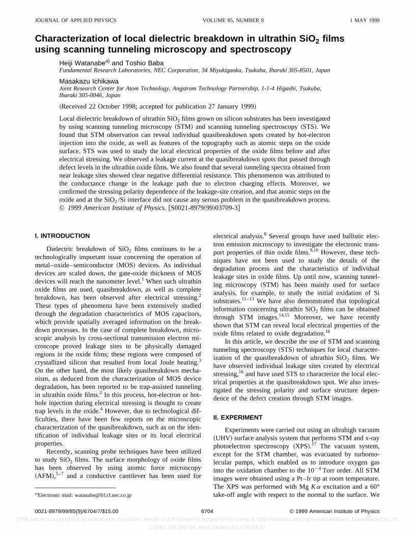
Figure 1 shows a STM image of a 1-nm-thick SiO2 filmgrown on a Si~111! substrate. We can see a step structure,which originates from the initial Si substrate. Observation ofthis step means that layer-by-layer oxidation preserves theinitial surface morphology of the Si~111! substrate,18–21 andensures atomic-scale uniformity of the ultrathin oxide films.We also confirmed that STM observation under these condi-tions caused no changes in the oxide film.
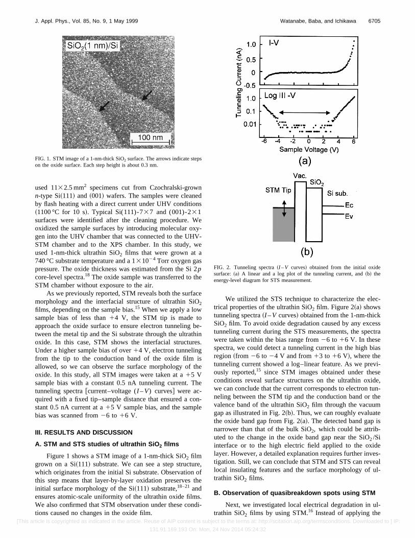
We utilized the STS technique to characterize the elec-trical properties of the ultrathin SiO2 film. Figure 2~a! showstunneling spectra~I –V curves! obtained from the 1-nm-thickSiO2 film. To avoid oxide degradation caused by any excesstunneling current during the STS measurements, the spectrawere taken within the bias range from26 to 16 V. In thesespectra, we could detect a tunneling current in the high biasregion~from 26 to 24 V and from13 to 16 V!, where thetunneling current showed a log–linear feature. As we previ-ously reported,15 since STM images obtained under theseconditions reveal surface structures on the ultrathin oxide,we can conclude that the current corresponds to electron tun-neling between the STM tip and the conduction band or thevalence band of the ultrathin SiO2 film through the vacuumgap as illustrated in Fig. 2~b!. Thus, we can roughly evaluatethe oxide band gap from Fig. 2~a!. The detected band gap isnarrower than that of the bulk SiO2, which could be attrib-uted to the change in the oxide band gap near the SiO2/Siinterface or to the high electric field applied to the oxidelayer. However, a detailed explanation requires further inves-tigation. Still, we can conclude that STM and STS can reveallocal insulating features and the surface morphology of ul-trathin SiO2 films.
B. Observation of quasibreakdown spots using STM
Next, we investigated local electrical degradation in ul-trathin SiO2 films by using STM.16 Instead of applying the
FIG. 1. STM image of a 1-nm-thick SiO2 surface. The arrows indicate stepson the oxide surface. Each step height is about 0.3 nm.
FIG. 2. Tunneling spectra~I –V curves! obtained from the initial oxidesurface:~a! A linear and a log plot of the tunneling current, and~b! theenergy-level diagram for STS measurement.
6705J. Appl. Phys., Vol. 85, No. 9, 1 May 1999 Watanabe, Baba, and Ichikawa
[This article is copyrighted as indicated in the article. Reuse of AIP content is subject to the terms at: http://scitation.aip.org/termsconditions. Downloaded to ] IP:
131.91.169.193 On: Mon, 24 Nov 2014 05:24:32
conventional stressing method to MOS capacitors,2 we de-graded ultrathin SiO2 films through hot-electron injectionfrom the STM tip into the oxide films. The tip was scannedover a 1003100 mm2 area at a110 V sample bias and witha constant current of 6 nA, enabling hot electrons to be in-jected from the STM tip to the oxide by Fowler–Nordheimtunneling. Under these conditions, the tip–sample distancewas increased compared with that during surface observationat a 15 V sample bias. Assuming the tip–sample distanceranged from 1 to 2 nm, the electric field applied to the oxidelayer would correspond to the order of 10 MV/cm. In addi-tion, since we scanned the STM tip under a constant tunnel-ing current of 6 nA, the Joule heating was unlikely to causea complete breakdown of the oxide.
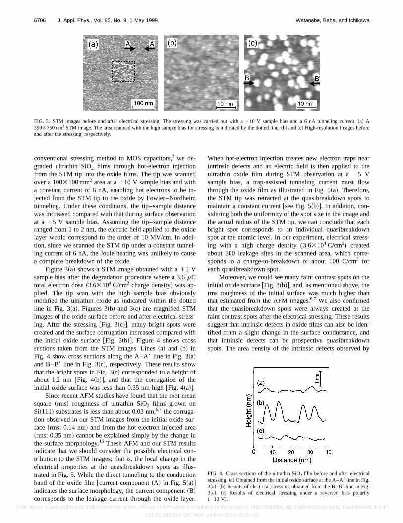
Figure 3~a! shows a STM image obtained with a15 Vsample bias after the degradation procedure where a 3.6mCtotal electron dose~3.63104 C/cm2 charge density! was ap-plied. The tip scan with the high sample bias obviouslymodified the ultrathin oxide as indicated within the dottedline in Fig. 3~a!. Figures 3~b! and 3~c! are magnified STMimages of the oxide surface before and after electrical stress-ing. After the stressing@Fig. 3~c!#, many bright spots werecreated and the surface corrugation increased compared withthe initial oxide surface@Fig. 3~b!#. Figure 4 shows crosssections taken from the STM images. Lines~a! and ~b! inFig. 4 show cross sections along the A–A8 line in Fig. 3~a!and B–B8 line in Fig. 3~c!, respectively. These results showthat the bright spots in Fig. 3~c! corresponded to a height ofabout 1.2 nm@Fig. 4~b!#, and that the corrugation of theinitial oxide surface was less than 0.35 nm high@Fig. 4~a!#.
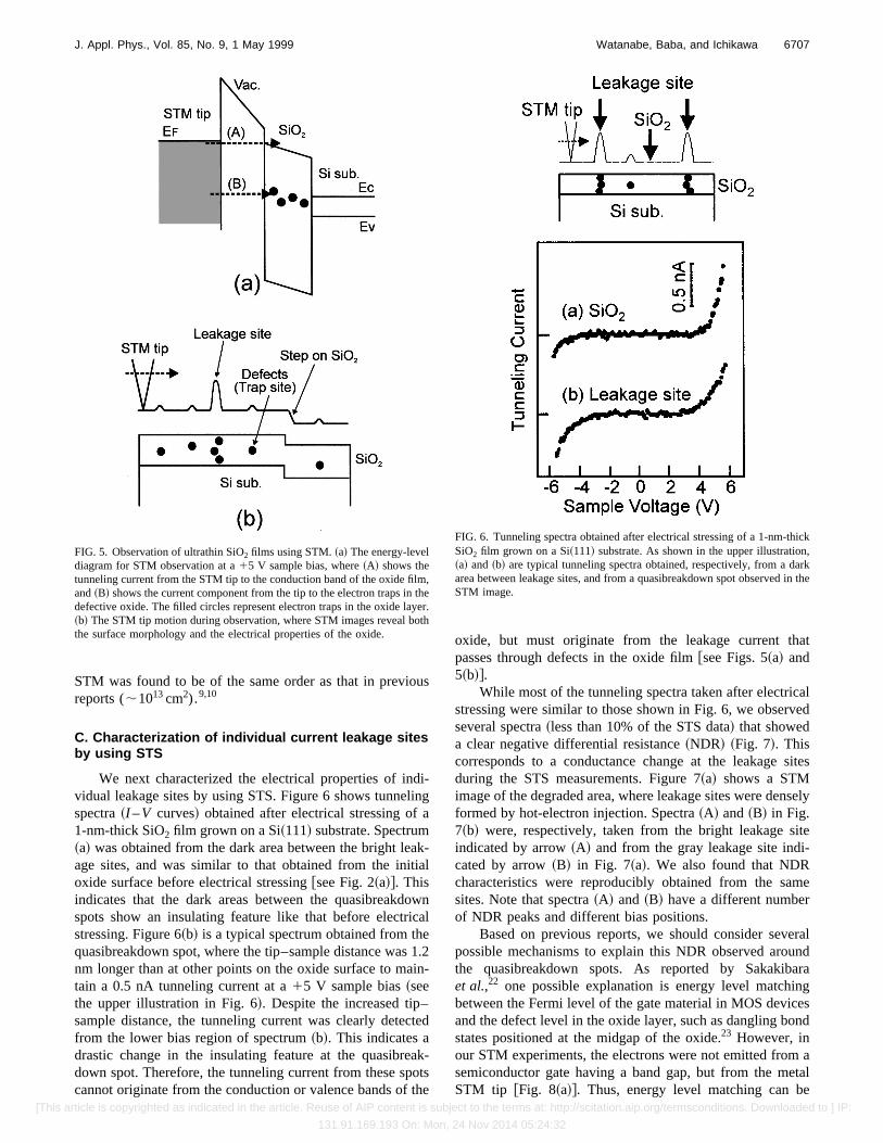
Since recent AFM studies have found that the root meansquare~rms! roughness of ultrathin SiO2 films grown onSi~111! substrates is less than about 0.03 nm,6,7 the corruga-tion observed in our STM images from the initial oxide sur-face ~rms: 0.14 nm! and from the hot-electron injected area~rms: 0.35 nm! cannot be explained simply by the change inthe surface morphology.16 These AFM and our STM resultsindicate that we should consider the possible electrical con-tribution to the STM images; that is, the local change in theelectrical properties at the quasibreakdown spots as illus-trated in Fig. 5. While the direct tunneling to the conductionband of the oxide film@current component~A! in Fig. 5~a!#indicates the surface morphology, the current component~B!corresponds to the leakage current through the oxide layer.
When hot-electron injection creates new electron traps nearintrinsic defects and an electric field is then applied to theultrathin oxide film during STM observation at a15 Vsample bias, a trap-assisted tunneling current must flowthrough the oxide film as illustrated in Fig. 5~a!. Therefore,the STM tip was retracted at the quasibreakdown spots tomaintain a constant current@see Fig. 5~b!#. In addition, con-sidering both the uniformity of the spot size in the image andthe actual radius of the STM tip, we can conclude that eachbright spot corresponds to an individual quasibreakdownspot at the atomic level. In our experiment, electrical stress-ing with a high charge density (3.63104 C/cm2) createdabout 300 leakage sites in the scanned area, which corre-sponds to a charge-to-breakdown of about 100 C/cm2 foreach quasibreakdown spot.
Moreover, we could see many faint contrast spots on theinitial oxide surface@Fig. 3~b!#, and, as mentioned above, therms roughness of the initial surface was much higher thanthat estimated from the AFM images.6,7 We also confirmedthat the quasibreakdown spots were always created at thefaint contrast spots after the electrical stressing. These resultssuggest that intrinsic defects in oxide films can also be iden-tified from a slight change in the surface conductance, andthat intrinsic defects can be prospective quasibreakdownspots. The area density of the intrinsic defects observed by
FIG. 3. STM images before and after electrical stressing. The stressing was carried out with a110 V sample bias and a 6 nA tunneling current.~a! A3503350 nm2 STM image. The area scanned with the high sample bias for stressing is indicated by the dotted line.~b! and~c! High-resolution images beforeand after the stressing, respectively.
FIG. 4. Cross sections of the ultrathin SiO2 film before and after electricalstressing.~a! Obtained from the initial oxide surface at the A–A8 line in Fig.3~a!. ~b! Results of electrical stressing obtained from the B–B8 line in Fig.3~c!. ~c! Results of electrical stressing under a reversed bias polarity~210 V!.
6706 J. Appl. Phys., Vol. 85, No. 9, 1 May 1999 Watanabe, Baba, and Ichikawa
[This article is copyrighted as indicated in the article. Reuse of AIP content is subject to the terms at: http://scitation.aip.org/termsconditions. Downloaded to ] IP:
131.91.169.193 On: Mon, 24 Nov 2014 05:24:32
STM was found to be of the same order as that in previousreports (;1013cm2).9,10
C. Characterization of individual current leakage sitesby using STS
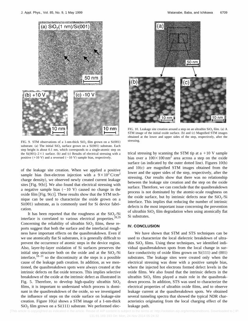
We next characterized the electrical properties of indi-vidual leakage sites by using STS. Figure 6 shows tunnelingspectra~I –V curves! obtained after electrical stressing of a1-nm-thick SiO2 film grown on a Si~111! substrate. Spectrum~a! was obtained from the dark area between the bright leak-age sites, and was similar to that obtained from the initialoxide surface before electrical stressing@see Fig. 2~a!#. Thisindicates that the dark areas between the quasibreakdownspots show an insulating feature like that before electricalstressing. Figure 6~b! is a typical spectrum obtained from thequasibreakdown spot, where the tip–sample distance was 1.2nm longer than at other points on the oxide surface to main-tain a 0.5 nA tunneling current at a15 V sample bias~seethe upper illustration in Fig. 6!. Despite the increased tip–sample distance, the tunneling current was clearly detectedfrom the lower bias region of spectrum~b!. This indicates adrastic change in the insulating feature at the quasibreak-down spot. Therefore, the tunneling current from these spotscannot originate from the conduction or valence bands of the
oxide, but must originate from the leakage current thatpasses through defects in the oxide film@see Figs. 5~a! and5~b!#.
While most of the tunneling spectra taken after electricalstressing were similar to those shown in Fig. 6, we observedseveral spectra~less than 10% of the STS data! that showeda clear negative differential resistance~NDR! ~Fig. 7!. Thiscorresponds to a conductance change at the leakage sitesduring the STS measurements. Figure 7~a! shows a STMimage of the degraded area, where leakage sites were denselyformed by hot-electron injection. Spectra~A! and~B! in Fig.7~b! were, respectively, taken from the bright leakage siteindicated by arrow~A! and from the gray leakage site indi-cated by arrow~B! in Fig. 7~a!. We also found that NDRcharacteristics were reproducibly obtained from the samesites. Note that spectra~A! and ~B! have a different numberof NDR peaks and different bias positions.
Based on previous reports, we should consider severalpossible mechanisms to explain this NDR observed aroundthe quasibreakdown spots. As reported by Sakakibaraet al.,22 one possible explanation is energy level matchingbetween the Fermi level of the gate material in MOS devicesand the defect level in the oxide layer, such as dangling bondstates positioned at the midgap of the oxide.23 However, inour STM experiments, the electrons were not emitted from asemiconductor gate having a band gap, but from the metalSTM tip @Fig. 8~a!#. Thus, energy level matching can be
FIG. 5. Observation of ultrathin SiO2 films using STM.~a! The energy-leveldiagram for STM observation at a15 V sample bias, where~A! shows thetunneling current from the STM tip to the conduction band of the oxide film,and~B! shows the current component from the tip to the electron traps in thedefective oxide. The filled circles represent electron traps in the oxide layer.~b! The STM tip motion during observation, where STM images reveal boththe surface morphology and the electrical properties of the oxide.
FIG. 6. Tunneling spectra obtained after electrical stressing of a 1-nm-thickSiO2 film grown on a Si~111! substrate. As shown in the upper illustration,~a! and~b! are typical tunneling spectra obtained, respectively, from a darkarea between leakage sites, and from a quasibreakdown spot observed in theSTM image.
6707J. Appl. Phys., Vol. 85, No. 9, 1 May 1999 Watanabe, Baba, and Ichikawa
[This article is copyrighted as indicated in the article. Reuse of AIP content is subject to the terms at: http://scitation.aip.org/termsconditions. Downloaded to ] IP:
131.91.169.193 On: Mon, 24 Nov 2014 05:24:32
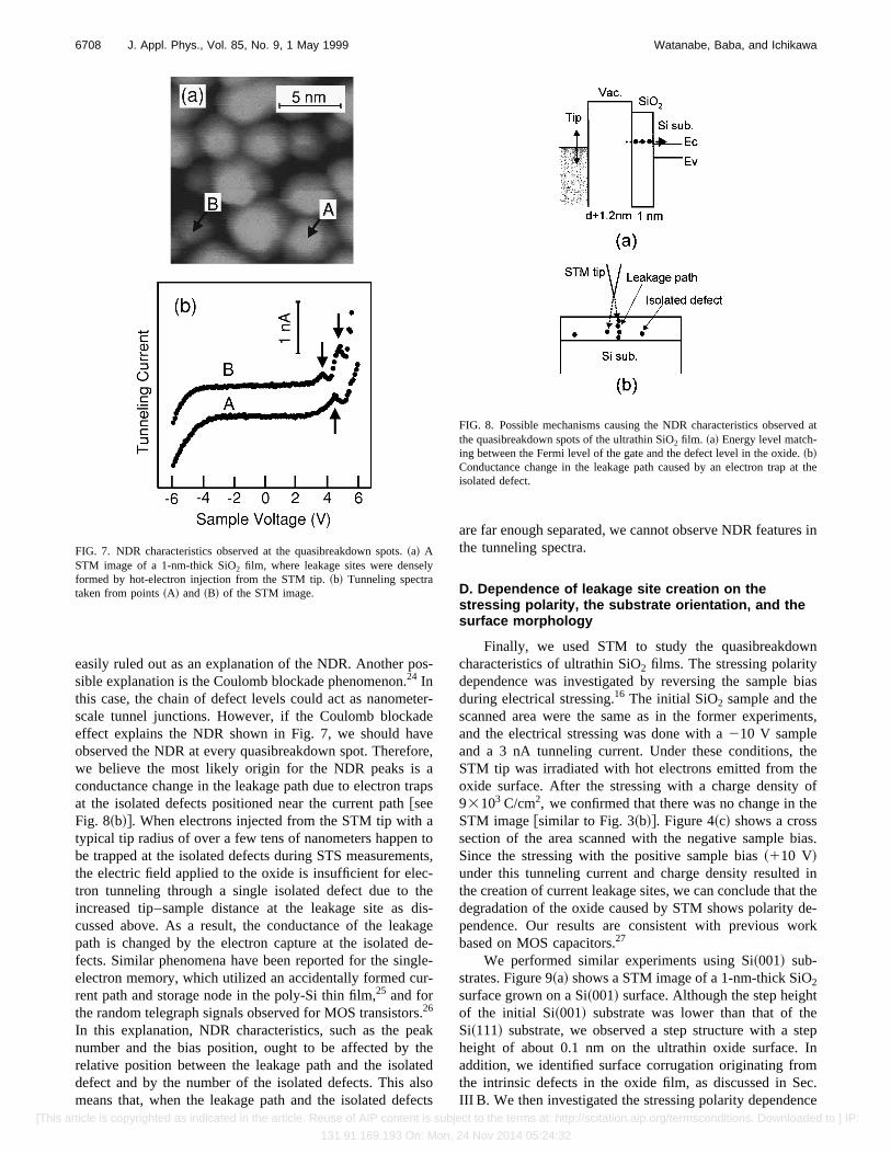
easily ruled out as an explanation of the NDR. Another pos-sible explanation is the Coulomb blockade phenomenon.24 Inthis case, the chain of defect levels could act as nanometer-scale tunnel junctions. However, if the Coulomb blockadeeffect explains the NDR shown in Fig. 7, we should haveobserved the NDR at every quasibreakdown spot. Therefore,we believe the most likely origin for the NDR peaks is aconductance change in the leakage path due to electron trapsat the isolated defects positioned near the current path@seeFig. 8~b!#. When electrons injected from the STM tip with atypical tip radius of over a few tens of nanometers happen tobe trapped at the isolated defects during STS measurements,the electric field applied to the oxide is insufficient for elec-tron tunneling through a single isolated defect due to theincreased tip–sample distance at the leakage site as dis-cussed above. As a result, the conductance of the leakagepath is changed by the electron capture at the isolated de-fects. Similar phenomena have been reported for the single-electron memory, which utilized an accidentally formed cur-rent path and storage node in the poly-Si thin film,25 and forthe random telegraph signals observed for MOS transistors.26
In this explanation, NDR characteristics, such as the peaknumber and the bias position, ought to be affected by therelative position between the leakage path and the isolateddefect and by the number of the isolated defects. This alsomeans that, when the leakage path and the isolated defects
are far enough separated, we cannot observe NDR features inthe tunneling spectra.
D. Dependence of leakage site creation on thestressing polarity, the substrate orientation, and thesurface morphology
Finally, we used STM to study the quasibreakdowncharacteristics of ultrathin SiO2 films. The stressing polaritydependence was investigated by reversing the sample biasduring electrical stressing.16 The initial SiO2 sample and thescanned area were the same as in the former experiments,and the electrical stressing was done with a210 V sampleand a 3 nA tunneling current. Under these conditions, theSTM tip was irradiated with hot electrons emitted from theoxide surface. After the stressing with a charge density of93103 C/cm2, we confirmed that there was no change in theSTM image@similar to Fig. 3~b!#. Figure 4~c! shows a crosssection of the area scanned with the negative sample bias.Since the stressing with the positive sample bias~110 V!under this tunneling current and charge density resulted inthe creation of current leakage sites, we can conclude that thedegradation of the oxide caused by STM shows polarity de-pendence. Our results are consistent with previous workbased on MOS capacitors.27
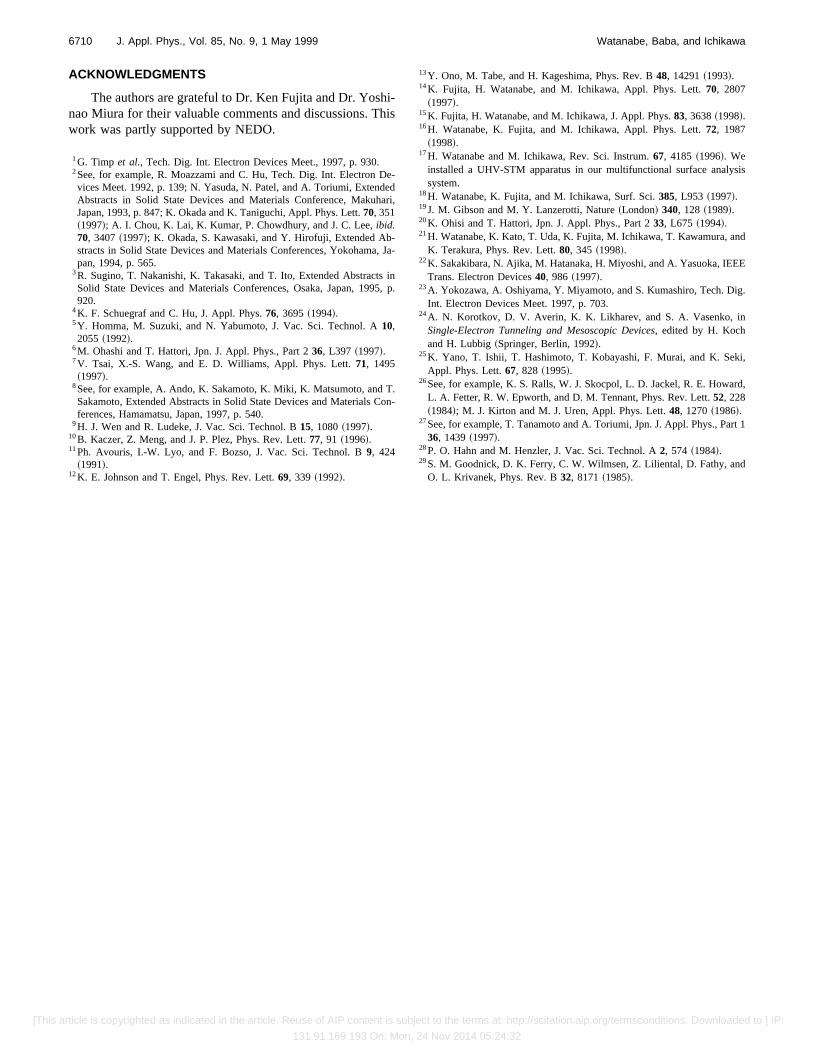
We performed similar experiments using Si~001! sub-strates. Figure 9~a! shows a STM image of a 1-nm-thick SiO2
surface grown on a Si~001! surface. Although the step heightof the initial Si~001! substrate was lower than that of theSi~111! substrate, we observed a step structure with a stepheight of about 0.1 nm on the ultrathin oxide surface. Inaddition, we identified surface corrugation originating fromthe intrinsic defects in the oxide film, as discussed in Sec.III B. We then investigated the stressing polarity dependence
FIG. 7. NDR characteristics observed at the quasibreakdown spots.~a! ASTM image of a 1-nm-thick SiO2 film, where leakage sites were denselyformed by hot-electron injection from the STM tip.~b! Tunneling spectrataken from points~A! and ~B! of the STM image.
FIG. 8. Possible mechanisms causing the NDR characteristics observed atthe quasibreakdown spots of the ultrathin SiO2 film. ~a! Energy level match-ing between the Fermi level of the gate and the defect level in the oxide.~b!Conductance change in the leakage path caused by an electron trap at theisolated defect.
6708 J. Appl. Phys., Vol. 85, No. 9, 1 May 1999 Watanabe, Baba, and Ichikawa
[This article is copyrighted as indicated in the article. Reuse of AIP content is subject to the terms at: http://scitation.aip.org/termsconditions. Downloaded to ] IP:
131.91.169.193 On: Mon, 24 Nov 2014 05:24:32
of the leakage site creation. When we applied a positivesample bias~hot-electron injection with a 93103 C/cm2
charge density!, we observed newly created current leakagesites@Fig. 9~b!#. We also found that electrical stressing witha negative sample bias~210 V! caused no change in theoxide film @Fig. 9~c!#. These results show that the STM tech-nique can be used to characterize the oxide grown on aSi~001! substrate, as is commonly used for Si device fabri-cation.
It has been reported that the roughness at the SiO2/Siinterface is correlated to various electrical properties.28,29
Concerning the reliability of ultrathin SiO2 films, these re-ports suggest that both the surface and the interfacial rough-ness have important effects on the quasibreakdown. Even ifwe use atomically flat Si substrates, it is generally difficult toprevent the occurrence of atomic steps in the device region.Also, layer-by-layer oxidation of Si surfaces preserves theinitial step structure both on the oxide and at the SiO2/Siinterface,18–21 so the discontinuity at the steps is a possiblecause of the leakage path creation. In addition, as we men-tioned, the quasibreakdown spots were always created at theintrinsic defects on flat oxide terraces. This implies selectivebreakdown of the oxide at the intrinsic defect as illustrated inFig. 5. Therefore, to develop high-quality ultrathin SiO2
films, it is important to understand which process is domi-nant in the quasibreakdown of the oxide, so we investigatedthe influence of steps on the oxide surface on leakage-sitecreation. Figure 10~a! shows a STM image of a 1-nm-thickSiO2 film grown on a Si~111! substrate. We performed elec-
trical stressing by scanning the STM tip at a110 V samplebias over a 1003100 nm2 area across a step on the oxidesurface~as indicated by the outer dotted line!. Figures 10~b!and 10~c! are magnified STM images obtained from thelower and the upper sides of the step, respectively, after thestressing. Our results show that there was no relationshipbetween the leakage site creation and the step on the oxidesurface. Therefore, we can conclude that the quasibreakdownprocess is not dominated by the atomic-scale roughness onthe oxide surface, but by intrinsic defects near the SiO2/Siinterface. This implies that reducing the number of intrinsicdefects is the most important issue concerning the preventionof ultrathin SiO2 film degradation when using atomically flatSi substrates.
IV. CONCLUSION
We have shown that STM and STS techniques can beused to characterize the local dielectric breakdown of ultra-thin SiO2 films. Using these techniques, we identified indi-vidual quasibreakdown spots from the local change in sur-face conductivity of oxide films grown on Si~111! and~001!substrates. The leakage sites were created only when theelectrical stressing was done with a positive sample bias,where the injected hot electrons formed defect levels in theoxide films. We also found that the intrinsic defects in theultrathin SiO2 films played a main role in the quasibreak-down process. In addition, STS was used to characterize theelectrical properties of ultrathin oxide films, and to observeleakage current at the quasibreakdown spots. We obtainedseveral tunneling spectra that showed the typical NDR char-acteristics originating from the local charging effect of theleakage path.
FIG. 9. STM observations of a 1-nm-thick SiO2 film grown on a Si~001!substrate.~a! The initial SiO2 surface grown on a Si~001! substrate. Eachstep height is about 0.1 nm, which corresponds to a single-atomic step onthe Si(001)-231 surface.~b! and ~c! Results of electrical stressing with apositive ~110 V! and a reversed~210 V! sample bias, respectively.
FIG. 10. Leakage site creation around a step on an ultrathin SiO2 film. ~a! ASTM image of the initial oxide surface.~b! and~c! Magnified STM imagesobtained at the lower and upper sides of the step, respectively, after thestressing.
6709J. Appl. Phys., Vol. 85, No. 9, 1 May 1999 Watanabe, Baba, and Ichikawa
[This article is copyrighted as indicated in the article. Reuse of AIP content is subject to the terms at: http://scitation.aip.org/termsconditions. Downloaded to ] IP:
131.91.169.193 On: Mon, 24 Nov 2014 05:24:32
ACKNOWLEDGMENTS
The authors are grateful to Dr. Ken Fujita and Dr. Yoshi-nao Miura for their valuable comments and discussions. Thiswork was partly supported by NEDO.
1G. Timp et al., Tech. Dig. Int. Electron Devices Meet., 1997, p. 930.2See, for example, R. Moazzami and C. Hu, Tech. Dig. Int. Electron De-vices Meet. 1992, p. 139; N. Yasuda, N. Patel, and A. Toriumi, ExtendedAbstracts in Solid State Devices and Materials Conference, Makuhari,Japan, 1993, p. 847; K. Okada and K. Taniguchi, Appl. Phys. Lett.70, 351~1997!; A. I. Chou, K. Lai, K. Kumar, P. Chowdhury, and J. C. Lee,ibid.70, 3407~1997!; K. Okada, S. Kawasaki, and Y. Hirofuji, Extended Ab-stracts in Solid State Devices and Materials Conferences, Yokohama, Ja-pan, 1994, p. 565.
3R. Sugino, T. Nakanishi, K. Takasaki, and T. Ito, Extended Abstracts inSolid State Devices and Materials Conferences, Osaka, Japan, 1995, p.920.
4K. F. Schuegraf and C. Hu, J. Appl. Phys.76, 3695~1994!.5Y. Homma, M. Suzuki, and N. Yabumoto, J. Vac. Sci. Technol. A10,2055 ~1992!.
6M. Ohashi and T. Hattori, Jpn. J. Appl. Phys., Part 236, L397 ~1997!.7V. Tsai, X.-S. Wang, and E. D. Williams, Appl. Phys. Lett.71, 1495~1997!.
8See, for example, A. Ando, K. Sakamoto, K. Miki, K. Matsumoto, and T.Sakamoto, Extended Abstracts in Solid State Devices and Materials Con-ferences, Hamamatsu, Japan, 1997, p. 540.
9H. J. Wen and R. Ludeke, J. Vac. Sci. Technol. B15, 1080~1997!.10B. Kaczer, Z. Meng, and J. P. Plez, Phys. Rev. Lett.77, 91 ~1996!.11Ph. Avouris, I.-W. Lyo, and F. Bozso, J. Vac. Sci. Technol. B9, 424
~1991!.12K. E. Johnson and T. Engel, Phys. Rev. Lett.69, 339 ~1992!.
13Y. Ono, M. Tabe, and H. Kageshima, Phys. Rev. B48, 14291~1993!.14K. Fujita, H. Watanabe, and M. Ichikawa, Appl. Phys. Lett.70, 2807
~1997!.15K. Fujita, H. Watanabe, and M. Ichikawa, J. Appl. Phys.83, 3638~1998!.16H. Watanabe, K. Fujita, and M. Ichikawa, Appl. Phys. Lett.72, 1987
~1998!.17H. Watanabe and M. Ichikawa, Rev. Sci. Instrum.67, 4185 ~1996!. We
installed a UHV-STM apparatus in our multifunctional surface analysissystem.
18H. Watanabe, K. Fujita, and M. Ichikawa, Surf. Sci.385, L953 ~1997!.19J. M. Gibson and M. Y. Lanzerotti, Nature~London! 340, 128 ~1989!.20K. Ohisi and T. Hattori, Jpn. J. Appl. Phys., Part 233, L675 ~1994!.21H. Watanabe, K. Kato, T. Uda, K. Fujita, M. Ichikawa, T. Kawamura, and
K. Terakura, Phys. Rev. Lett.80, 345 ~1998!.22K. Sakakibara, N. Ajika, M. Hatanaka, H. Miyoshi, and A. Yasuoka, IEEE
Trans. Electron Devices40, 986 ~1997!.23A. Yokozawa, A. Oshiyama, Y. Miyamoto, and S. Kumashiro, Tech. Dig.
Int. Electron Devices Meet. 1997, p. 703.24A. N. Korotkov, D. V. Averin, K. K. Likharev, and S. A. Vasenko, in
Single-Electron Tunneling and Mesoscopic Devices, edited by H. Kochand H. Lubbig~Springer, Berlin, 1992!.
25K. Yano, T. Ishii, T. Hashimoto, T. Kobayashi, F. Murai, and K. Seki,Appl. Phys. Lett.67, 828 ~1995!.
26See, for example, K. S. Ralls, W. J. Skocpol, L. D. Jackel, R. E. Howard,L. A. Fetter, R. W. Epworth, and D. M. Tennant, Phys. Rev. Lett.52, 228~1984!; M. J. Kirton and M. J. Uren, Appl. Phys. Lett.48, 1270~1986!.
27See, for example, T. Tanamoto and A. Toriumi, Jpn. J. Appl. Phys., Part 136, 1439~1997!.
28P. O. Hahn and M. Henzler, J. Vac. Sci. Technol. A2, 574 ~1984!.29S. M. Goodnick, D. K. Ferry, C. W. Wilmsen, Z. Liliental, D. Fathy, and
O. L. Krivanek, Phys. Rev. B32, 8171~1985!.
6710 J. Appl. Phys., Vol. 85, No. 9, 1 May 1999 Watanabe, Baba, and Ichikawa
[This article is copyrighted as indicated in the article. Reuse of AIP content is subject to the terms at: http://scitation.aip.org/termsconditions. Downloaded to ] IP:
131.91.169.193 On: Mon, 24 Nov 2014 05:24:32

本文献由“学霸图书馆-文献云下载”收集自网络,仅供学习交流使用。
学霸图书馆(www.xuebalib.com)是一个“整合众多图书馆数据库资源,
提供一站式文献检索和下载服务”的24 小时在线不限IP
图书馆。
图书馆致力于便利、促进学习与科研,提供最强文献下载服务。
图书馆导航:
图书馆首页 文献云下载 图书馆入口 外文数据库大全 疑难文献辅助工具