HIGH VOLTAGE SUBNANOSECOND DIELECTRIC …privat.bahnhof.se/wb907234/pics/31295012202627.pdfhigh...
110
? HIGH VOLTAGE SUBNANOSECOND DIELECTRIC BREAKDOWN by JOHN JEROME MANKOWSKI, B.S.E.E., M.S.E.E. A DISSERTATION IN ELECTRICAL ENGINEERING Submitted to the Graduate Faculty of Texas Tech University in Partial FulfiUment of the Requirements for the Degree of DOCTOR OF PHILOSOPHY ./ / /Approved December, 1997
Transcript of HIGH VOLTAGE SUBNANOSECOND DIELECTRIC …privat.bahnhof.se/wb907234/pics/31295012202627.pdfhigh...
?
HIGH VOLTAGE SUBNANOSECOND DIELECTRIC
BREAKDOWN
by
JOHN JEROME MANKOWSKI, B.S.E.E., M.S.E.E.
A DISSERTATION
IN
ELECTRICAL ENGINEERING
Submitted to the Graduate Faculty of Texas Tech University in
Partial FulfiUment of the Requirements for
the Degree of
DOCTOR OF PHILOSOPHY
./ / /Approved
December, 1997
ACKNOWLEDGEMENTS
I would like to express my appreciation to Dr. M. Kristiansen for his support and
technical advice during this research project. I would also like to thank the other
members of my conMnittee, Dr. L. Hatfield, Dr. M. Giesselmann, and Dr. H. Krompholz
for their guidance. I am also grateful to Dr. J. Dickens for his direction and advice in the
designing and building of the necessary hardware to complete this project.
I am indebted to the USAF Phillips Laboratory, especially Dr. F.J. Agee and W.
Prather, for their direction and AFOSR/MURI for the financial support of this project.
Finally, I would like to thank my family and especially my girlfriend, Amanda,
who has provided support and encouragement throughout this last year.
11
E=BC
TABLE OF CONTENTS
ACKNOWLEDGEMENTS ii
ABSTRACT v
LISTOFHGURES vi
CHAPTER
L INTRODUCTION 1
n. THEORY OF ELECTRICAL BREAKDOWN 3
Introduction 3
Townsend Breakdown 3
Paschen'sLaw 7
Streamer Theory 8
Dielectric Breakdown Strength Dependence on Voltage Polarity 16
Time Lag of Pulsed Breakdown 19
Liquid Dielectric Breakdown 22
ffl. EXPERIMENTAL SETUP 27
Introduction 27
SEF-303A Nanosecond Pulser 27
Marx Bank Driven PEL Pulser 32
UV Radiation Semp 38
Streak Camera Semp 38
Test Gap 41
111
IV. DL\GNOSTICS 48
Introduction 48
High Voltage Dividers 48
Umbrella Probe 54
Probe Design 58
Diagnostic Semp 59
Probe Calibration 62
V. EXPERIMENTAL RESULTS 68
Introduction 68
E-field versus Breakdown Time for Gases 68
An Empirical Relationship for Gas Breakdown 76
E-field versus Breakdown Time for Liquids 78
An Empirical Relationship for Transformer Oil Breakdown 79
Dielectric Breakdown Strength Dependence on Polarity 81
Streak Camera Images 82
Effect of Ultraviolet Radiation on Statistical Lag Time 87
VL CONCLUSIONS 96
REFERENCES 98
IV
ABSTRACT
Current interests in ultrawideband radar sources are in the microwave regime,
which corresponds to voltage pulse risetimes less than a nanosecond. Some new sources,
including the PhiUips Laboratory Hindenberg series of hydrogen gas switched pulsers, use
hydrogen at hundreds of atmospheres of pressure in the switch. Unfortunately, the
published data of electrical breakdown of gas and liquid media at times less than a
nanosecond are relatively scarce.
A smdy was conducted on the electrical breakdown properties of liquid and gas
dielectrics at subnanosecond and nanoseconds. Two separate voltage sources with pulse
risetimes less than 400 ps were developed. Diagnostic probes were designed and tested for
their capability of detecting high voltage pulses at these fast risetimes.
A thorough investigation into E-field strengths of hquid and gas dielectrics at
breakdown times ranging from 0.4 to 5 ns was performed. The breakdown strength
dependence on voltage polarity was observed. Streak camera images of streamer formation
were taken. The effect of ultraviolet radiation, incident upon the gap, on statistical lag time
was determined.

LIST OF FIGURES
2.1. Current-voltage relationship of gas gap 4
2.2. Paschen curve for various gases 8
2.3. E-field distribution across the gap including the effect of space charge 9
2.4. Sketch of the propagation of a streamer due to ionized gas
ft"om radiation, (a) Anode directed (b) Cathode directed 10
2.5. Formative time measurements for air 13
2.6. Typical breakdown trigger current of a trigatron 15
2.7. Breakdown times for various gases 16
2.8. DC breakdown voltage for SF6 rod-plane gap (distance from rod to plane d = 20 mm, rod radius r = 1 mm) 17
2.9. Diagram of positive point with space charge including E-field strength distribution between positive point and grounded plane with and without space charge 18
2.10. Diagram of negative point with space charge including E-field strength distribution between negative point and grounded plane with and without space charge 19
2.11. Time lag compenents under a step voltage. Vg static breakdown voltage,
Vp peak voltage, ts statistical lag time, tf formative time 20
2.12. Histograms of observational delay time, (a) Brass (b) Graphite 21
2.13. Histograms of observational delay time for various overvoltages 22
2.14. Streamer velocity in transformer oil. (a) positive polarity (b) negative polarity ....24
2.15. E-field strength versus breakdown time for transformer oil 25
2.16. Various breakdown data for transformer oil 26
3.1. SEF-303A compact pulsed power source 28
VI

3.2 Traces of charging voltage of the forming line
and of the output voltage at different load resistances 29
3.3. Experimental setup with SEF-303A pulser 29
3.4. Voltage output of SEF-303A pulser into experimental semp 30
3.5. Experimental setup of SEF-303 A with peaking gap 31
3.6. Photograph of the SEF-303A with peaking gap experimental setup 31
3.7. Gap voltages from the SEF-303A with and without peaking gap 32
3.8. Marx bank driven PEL subnanosecond pulser 32
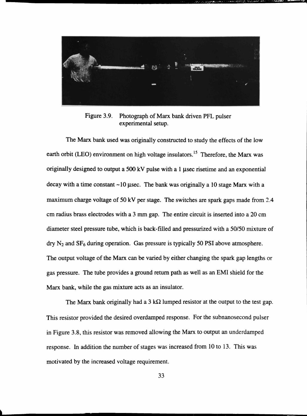
3.9. Photograph of Marx bank driven PEL pulser experimental setup 33
3.10. Equivalent circuits of Marx bank driven PEL. (a) DC state (b) Erected Marx 34
3.11. Charging voltage of the PEL (a) Simulated (b) Acmal 36
3.12. Test gap voltage from the Marx bank driven PEL 37
3.13. Transmittance of a 1 cm thick ultraviolet grade fused silica 38
3.14. Schemetic of the Hamamatsu streak camera 39
3.15. Schematic of the experimental setup with streak camera 40
3.16. Test chamber for the experimental setup 41
3.17. Photograph of the hemispherical brass electrodes 41
3.18. Photograph of the point-plane geometry electrodes 42
3.19. Plot of maximum and average E-field vs gap distance 43
3.20 E-field strength plot using Maxwell 3D for hemispherical electrodes
and 500 kV gap voltage: (a) 5 mm gap, (b) 1 cm gap, (c) 2 cm gap 44
3.21. E-field at point tip and average E-field across the gap vs gap distance 45
3.22. E-field strength plots for test chamber with point-plane electrodes and 500 kV gap voltage: (a) 1 mm gap, (b) 2 mm gap, (c) 5 mm gap 46
Vll

4.1. Equivalent circuit of a resistive divider 49
4.2. Step response of a resistive divider with R<i = 0 Q 49
4.3. Schematic of a typical capacitive divider 50
4.4. Circuit equivalent of a typical capacitive divider 50
4.5. Measured step response of a capacitor divider at different time scales 52
4.6. A dense dielectric supported stripline E-field sensor 53
4.7. Step response of the dense dielectric supported stripline E-field sensor 54
4.8. Coaxial line with umbrella probe 55
4.9. Close-up view of a capacitive probe 59
4.10. Diagnostic setup 59
4.11. Input reactance of an open-circuited transmission line 61
4.12. Diagram of an LTI system in the time domain 62
4.13. Diagram of an LTI system in the frequency domain 63
4.14. Calibration setup of frequency and phase response test 64
4.15. Frequency magnimde response of a CVD 64
4.16. Phase response of a CVD 64
4.17. Normalized frequency response of
compensated and uncompensated waveforms 65
4.18. Normalized voltage of compensated and uncompensated waveforms 66
4.19. Calibration setup with known input pulse 66
4.20. Normalized voltage of the applied pulse and CVD pulse 67
5.1. Voltage waveforms at the cathode and anode for H2 at 9 MPa (1300 psi) and 1.8 mm gap spacing 69
5.2. Peak E-field versus time to breakdown for various gases 70
viii

5.3. E-field versus breakdown time scaled with gas pressure for various gases 70
5.4. E-field versus breakdown time for air with breakdown times down to 6(X) ps 71
5.5. Paschen curve for various gases 72
5.6. Comparison between F & P and author's data of breakdown in air 73
5.7. Collected gas breakdown data compared with the Martin curve 74
5.8. Breakdown data for various gases including Martin curve.
Also shows curve fit of selected data 77
5.9. Peak E-field versus time to breakdown for various liquid dielectrics 78
5.10. Breakdown data for transformer oil 79
5.11. Empirical curve fit for collected transformer oil breakdown data 80
5.12. Breakdown data for point-plane geometry in transformer oil 81
5.13. Breakdown data of a point-plane geometry in air 82
5.14. 5 ns streak of 1 mm transformer oil gap after arc formation 83
5.15. Streak images of the beginning of the arc formation of a 1mm
transformer oil gap at time lengths of (a) 5 ns and (b) 10 ns 84
5.16. Close-up view of arc formation in the 5 ns streak 85
5.17. Streak image of the beginning of arc formation of a 2.8 MPa (4(X) psi), 4 mm air gap at a 10 ns sweep 86
5.18. Streak image of the beginning of arc formation of a 2.8 MPa (400) psi, 4 mm air gap at a 5 ns sweep 86
5.19. Close-up view of the arc formation of the 2.8 MPa (4(X) psi), 4 mm air gap at a 5 ns sweep 87
5.20. Distribution of breakdown times in H2 for (a) lOlkPa (14.7 psi) with a 4.5 mm gap, 50 kV gap voltage and (b) 1.4 kPa (200 psi) with a 4 mm gap, 200 kV gap voltage 88
IX
5.21. Median breakdown time of N2 at a gap length of 4 mm for various pressures with and without UV. Error bars are 1 standard deviation 91
5.22. Percent difference of median breakdown time between a nitrogen gap with and without UV radiation at various gap lengths versus gas pressure 92
5.23. Percent difference of median breakdown time between a nitrogen gap with and without UV radiation at various gap lengths versus E-field 92
5.24. Percent difference of median breakdown time between a nitrogen gap with and without UV radiation at various gap lengths versus E-field/pressure 93
5.25. Percent difference of median breakdown time between a hydrogen gap with and without UV radiation at various gap lengths versus E-field/pressure 94
5.26. Percent difference of median breakdown time between a helium gap with and without UV radiation at various gap lengths versus E-field/pressure 95
CHAPTER I
INTRODUCTION
Present interests in ultrawideband radiation sources are in the microwave regime,
which corresponds to voltage pulse risetimes less than a nanosecond.' The high
fi:equencies contained in the pulses provide oppormnities to develop information rich radar
systems. Some new sources, including the Phillips Laboratory Hindenberg series of
hydrogen gas switched pulsers use hydrogen at hundreds of atmospheres of pressure in the
switch.^ Unformnately, the published data of electrical breakdown of gas and hquid media
at times less than a nanosecond are relatively scarce. This dissertation is a part of the
research effort that is underway at the Phillips Laboratory and at a number of universities
related to research problems in high power microwaves and sponsored by the Air Force
Office of Scientific Research/MURI.
First, the theory of electrical breakdown is discussed. Topics such as Townsend
breakdown, Paschen's law, and ionization coefficients are briefly described. Streamer
theory is discussed in detail. Breakdown dependence on polarity and the statistical lag
present in pulsed breakdown are characterized. Also, the mechanisms of liquid breakdown
are discussed.
In the next chapter, the experimental semp is described. The operation and design
of the voltage sources used are discussed. These sources include the SEF-303 A pulser,
with and without an added peaking gap, and a Marx bank driven pulse forming line. The
setups of a UV effects and streak camera smdy are detailed. Also discussed is the design
and 3D-field simulation of the test gap.
The next chapter is dedicated to the diagnostic scheme used in the experimental
semp. An entire chapter is devoted to this subject due to the importance of accurate
diagnostics at these fast pulse risetimes. An investigation into the bandwidth of the
capacitive dividers utilized is described.
Next, the experimental results are presented. These results include E-field strengths
obtained for various gas and hquid dielectrics at breakdown times from 500 ps to 5 ns.
Additional data obtained include UV effect on statistical time lag, breakdown strength
dependence on voltage polarity, and streak camera images of the arc formation.
Finally, conclusions drawn from data obtained in the previous chapter are
presented.
CHAPTER n
THEORY OF ELECTRICAL BREAKDOWN
Introduction
Two major types of electrical breakdown are dc and pulsed. DC breakdown
decribes breakdown which occurs between electrodes which have had a voltage
difference for a long time (steady state). Pulsed breakdown describes breakdown which
occurs as a result of a fast voltage pulse between electrodes. The voltages required for
pulsed breakdown are typically 20% greater than voltages in dc breakdown. The
processes which comprise these two types of breakdown and related topics are described
in this chapter.
Townsend Breakdown
A state of equilibrium exists in an ordinary gas between the rate of electron and
positive ion generation and losses. However, when an external electric field is applied
this equilibrium is upset. Townsend first smdied the current generated in gases between
two parallel electrodes.
The V-I characteristic for an ordinary gas between parallel plate electrodes is
shown in Figure 2.1. As the gap voltage increases from zero to Vi the current increases
linearly. For a gap voltage between Vi and V2 the current remains constant at a value IQ.
This current, lo, is known as the saturation current and is the current generated when the
cathode is irradiated with UV light.
^ ^ B B S Z S S
Figure 2.1. Current-voltage relationship of gas gap.
Above a voltage V2, the electrons leaving the cathode are accelerated high enough
to cause ionization upon collision with gas molecules. Townsend defined the number of
electrons produced per unit length as the quantity a. Using Townsend's first ionization
coefficient the incremental increase of electrons is given as
dn = an dx. (2.1)
where n is the number of electrons at a distance x away from the cathode. Integrating this
equation over the distance, d, from cathode to anode gives
ocd
n = no e , (2.2)
where no is the number of primary electrons generated at the cathode. In terms of current
at the anode
1 = 106"^, (2.3)
where lo is the current leaving the cathode.
The ionization coefficient a is acmally dependent on the electron energy
distribudon in gas, which depends only on E/P, where E is the applied electric field and P
is the gas pressure. Therefore, a can be written as
a = Pf .P>
(2.4)
or
a _ fE)
" ' A P (2.5)
P
This dependence between a/P and E/P has been confirmed experimentally.
A number of other secondary processes contribute to the breakdown process.
Some of these include secondary electrons produced at the cathode by positive ion
impact, secondary electron emission at the cathode by photon impact, and ion impact
ionization of the gas. In order to account for these processes the Townsend second
ionization coefficient, y, is introduced. The steady state current equafion (2.3),
accounting for both Townsend coefficients, can be rewritten as
ad
where y may represent one or more possible mechanisms (y = Yi + Yph + .. )•
Experimental values for yean be determined from eqn. (2.6) for known values of
E, P, gap distance, and a. Values for y are highly dependent on cathode surface. Low
work function materials will produce greater emissions. The value of y is small at low
values of E/P and higher at greater values of E/P. This is to be expected since at high

values of E/P there will be a greater number of positive ions and photons with energies
high enough to eject electrons from the cathode.
Referring to equafion (2.6)
^ = 0 73^^71)'
Substituting eqn. (2.4) for a, eqn. (2.6) can be rewritten as
/' V ^
I = Io 7 7V^^' (2-7) (PdX
Pd 1 - y e ^™^-l y
As the gap voltage increases, the electrode current at the anode increases
according to equation (2.6). The current will increase until at some point the
denominator of eqn. (2.6) becomes zero, or
Y(e" ' - l )=l . (2.8)
At this point, eqn (2.6) predicts that the electrode current becomes infinite. This is
defined as the transition from self-sustained discharge to breakdown.
Theoretically, the value of the current becomes infinite, but in practice it is
limited by the external circuit and voltage drop across the gap. A self-sustaining
discharge occurs when the number of ion pairs produced in the gap by the passage of one
electron avalanche is large enough that the resulting positive ions, on bombarding the
cathode, are able to release one secondary electron and cause a repetition of the
avalanche process. The discharge may also be self-sustaining as a result of the secondary
electron photoemission process.
Paschen's Law
An analytic expression for breakdown voltage with respect to pressure and gap
distance can be derived from eqn. (2.4). Since the first Townsend coefficient can be
written as
a = Pf '5
eqn. (2.8) may be expressed as
(lh=i. (2.9)
Taking the namral logarithm of both sides of eqn. (2.9) results in.
In h V
/
= ln >
= K
rE y. f\ \ - P d = ln
Vi -Hi = K (2.10)
For a uniform field, Vb = Ed, the breakdown voltage can be written as
f\j \
, P d , Pd
Vb = (l)(Pd), (2.11)
which means the breakdown voltage is a function of the gas pressure and gap distance.
This relationship is known as the Paschen Law.
A Paschen curve for various gases^ is shown in Figure 2.2. Note that the
breakdown voltage goes through a minimum value at a particular (Pd)nun value. This
Vbmin can be explained qualitatively. For Pd > (Pd)min, electrons crossing the gap make
more frequent collisions than at (Pd)min, but the energy gained between collisions is less.
7
^ t J - ^ ^ - * " - -
This results in a lower ionization level for a given gap voltage. For Pd < (Pd)niin,
electrons crossing the gap make less frequent collisions than at (Pd)min. Therefore,
(Pd)min corresponds to the highest ionization frequency.
I0»
I » » -
- K C >
0.02
T-rr
-I0>
i -LJ
I—'—r-nri—r
I K) p.d(olni. mils)
I
K)«5
ipoo
Figure 2.2. Paschen curve for various gases.
Streamer Theory
Thus far, breakdown dependent mainly on electron ionization in the gas and ion
bombardment of the cathode has been discussed. However, for over-voltaged gaps
(typically 20% or higher of dc breakdown voltage) at pressures greater than lOO's of
Torr, much shorter breakdown delay times have been observed than what is predicted by
the ion drift velocity. This discrepancy led to the development of the streamer theory of
breakdown.
8
g«a5=
A streamer is started due to field enhancement at the head of the initial avalanche.
.10 A diagram of the electric field across the gap including the space charge distortion of
the initial avalanche is shown in Figure 2.3. The average field across the gap is Eo. The
electron and positive ion clouds are separated due to the higher mobility of the electrons.
The field at the anode side of the avalanche is enhanced. Between the electron and
positive ion clouds the field strength is reduced due to shielding from the E-field across
the gap. A field enhancement is also present at the cathode side of the avalanche.
' ^ r
(P^C
B{x\
Figure 2.3. E-field distribution across the gap including the effect of the space charge.'
When the carrier number in the initial avalanche reaches n = 10 , the field
enhancement becomes on the order of the applied field and may lead to the initiation of a
streamer. Once the avalanche reaches this critical size, the electron density at the head of
the anode side of the avalanche, which is in a highly enhanced E-field, begins to grow
rapidly towards the anode. This growth is due to photoionization, caused by ionizing
radiation generated at the avalanche head, and is called a streamer. This progression
moves at the speed of light due to the photon mechanism. At the cathode side of the
avalanche a similar process occurs. Electrons produced by photoionization are
accelerated toward the positive charge cloud head. This increases the size of the positive
charge cloud towards the cathode. Once the cathode is reached, breakdown occurs. A
schematic"* of the streamer process is shown in Figure 2.4.
Anode Anode
ff-Vz-) Photon
Cathode (a)
Cathode (b)
Figure 2.4. Sketch of the propagation of a streamer due to ionized gas from radiation, (a) Anode directed (b) Cathode directed."*
Raether has developed an empirical expression for the streamer initiated
breakdown formation
ax, = 17.7 -h In X, -h In — , E
(2.12)
where Er is the field strength at the anode side of the avalanche, Xc is the length of the
avalanche path in the field direction when it reaches the critical size. The condition for
criticality is Er = E, in which case eqn. (2.12) becomes
10

ax, =17.7-HIn X,. (2.13)
If Xc is larger than the gap length, then the initiation of streamers is unlikely.
Therefore, the minimum breakdown value by streamer mechanism is when Xc = d, where
d is the gap distance. Then eqn (2.13) becomes
ad = 17.7-Hlnd, (2.14)
which gives the minimum value of a for which streamer breakdown can occur.
Raether observed that a typical value for which streamer development can occur
is
axc = 20. (2.15)
Using this value he developed a formative time for breakdown. Since the streamer
propagation velocity is on the order of the speed of light, the formative time is the time it
takes an avalanche to become critical, or
t . . ^ . ^ , (2.16)
where Ve is the electron drift velocity.
Meek^ has developed a similar equation for streamer initiated breakdown. The
transition from avalanche to streamer breakdown is taken to be when the enhanced field
at the tail end of the avalanche due to the positive ions is on the order of the applied field.
This radial E-field at the tail end of the avalanche can be calculated from the expression
7 ae"" E, =5.3x10"' volts/cm, (2.17)
I P >
11
where x is the distance (in cm) which the avalanche has progressed and P is the gas
pressure in Torr. As before, letting Er = E and x = d, a minimum breakdown from
streamer occurs when
ad-h ln - = 14.5-Hln- + - l n - . (2.18) P P 2 p
Felsenthal and Proud have taken a slightly different approach. They show
analytically that under certain conditions, monopolar-pulsed and pulsed-microwave
breakdown are directly comparable. It is assumed that the field in the gap is undistorted
by the space charge. Also, effectively electrodeless monopolar-pulsed breakdown is
assumed.
The formative lag time is then the measured characteristic time for buildup of
ionization in the gap space. The electron continuity equation is used which relates the net
rate of change of electron density to the generation and loss mechanism,
— = V-n-v^n-V»r , (2.19)
where n is the electron density, Vi is the ionization frequency, Va is the attachment
frequency, and T is the particle flow. However, if the experimental design is such to
fulfill the requirement for an effectively electrodeless system, then the V»r term is
neglected. Equation (2.19) is modified to formulate predicted curves of E/P versus Px,
where T is the formative time to breakdown, for each of the gases studied. Writing the
ionization and attachment frequencies in terms of the Townsend first ionization
coefficient a and attachment coefficient p, this formula is
12
• • " ! • • ' ' • i . ' . i t t ^ i ' i ' i ' " ' ^
Px = ^n(nb/"o)
k(E/pXa/P-P/p)' (2.20)
where k(E/P) is the electron drift velocity which is dependent on E/P and nb/no is the ratio
of breakdown and initial electron densities.
Experimental results by Felsenthal and Proud matched well with this theoretical
model. Figure 2.5 shows formative time measurements in air compared with eqn. (2.20)
and data reported.
to
EIO' E E o
> 2 fO UJ
I I r MiiT[ r I I iiiiij I 1 t iiMn \ I I m m \ i i i im[ i i i itnn i i i i iiii
F & P Results
Gould ond Roberts Pultod Mierowov*
10 I ^-J" 1111 I I I I I I 11 I I I ' ' ' • " " ' I • • • i i i i t I I I ! m i l I . 1 1 m i l ' • " • •
10"' .o-» 10 I0-* »0 r5 10 - 4 10 r 3 10
- 2
P r (mm Hg tec)
Figure 2.5. Formative time measurements for air.
T.H. Martin^ takes a more empirical approach to breakdown delay. He has
developed a scaling relationship between the electric field and the breakdown time. Data
13
t .<i j ,^«>ff^M»,m.i„i .um.^.um*. 'JUjm.i^.^
were taken from many diverse experiments including laser-triggered switches, sharp
point to plane gaps, and uniform field gaps. The empirical relationship is given as
E pT = 9 7 8 0 q -
^r:V^^ (2.21)
where p is the gas density in gm/cm^, x is the time delay to breakdown in seconds, and E
is the electric field in kV/cm. One interesting observation can be made from this
relationship is that breakdown times are highly dependent on E and p.
Martin describes a tentative model for the electrical breakdown in the following
maimer. A fast discharge closes the gap in a short time compared with the overall
breakdown time. This fast discharge leaves behind a highly ionized channel. Electrical
energy is converted to thermal energy during a heating phase. During this phase there is
no significant change in the voltage across the gap. After many electron collisions, the
gas temperamre increases, thereby lowering the chaimel resistance. Finally, the gap
resistance drops to a point where the electrical driving circuit heats the channel more
efficiently. The gap resistance then drops rapidly along with the gap voltage to very low
values and the gap closes. The scaling with gas density in eqn. 2.21 is expected since the
relationship is one describing heating. Since the specific heats of most gases, except SFe,
are similar, the gas density becomes the important scaling factor.
This tentative model is based particularly on a typical trigger pre-breakdown
current for a trigatron, for which a waveform is shown in Figure 2.6. The fast discharge
in this waveform is short compared to the heating phase (5 ns to 3(X) ns). Unfortunately,
Martin does not speculate as to the nature of this fast discharge.
14

at
« 20-
Time in microseconds
Figure 2.6. Typical breakdown trigger current of a trigatron.
Figure 2.7 shows a plot of nitrogen, helium, SF6, and argon from the Felsenthal
and Proud^ database and also a plot of J.C. Martin^ data for air at 1 atm. As the plot
shows, the empirical relationship is rather good at long times and somewhat low at
shorter times. In fact, for all the data examined by T.H. Martin, it is the short time
Felsenthal and Proud data which are consistently above the predicted value. The
remaining data, all of which were at greater values of the product of gas density and
breakdown time, followed the empirical relationship closely.
15

^SBS
IMO
1*10 -O
^
B
> IMO
5 _
IMO
—
1
• •
•
•
• •
" ^ ^ " ^ ^
1
r
•
o
1
Empi N2 HE SF6 AR AIR
•
1 1
•
•
•
•
•
•
I 1
—
lMO-^5 IMO -14 1 . 1 0 - " i-io-'2 IMO -11 IMO -10
Pt (g/cc)(sec)
Figure 2.7. Breakdown times for various gases (F&P'-N2, He, Ar, and SFe, JCM^-air).
Dielectric Breakdown Strength Dependence on Voltage Polaritv
For point-plane like electrode geometries, the breakdown voltage is dependent on
the voltage polarity applied to the point electrode. In Figure 2.8 is shown polarity
dependence for SF6, where Vb is the breakdown voltage. ^ Notice that the breakdown
voltage is independent of polarity up to approximately 1.5 bar. This is due to the
establishment of a steady-state corona discharge about the positive point which acts to
stabilize the gap against breakdown. Above this pressure the stabilization ceases and the
breakdown for the positively charged point electrode falls to a consistently lower value.
16
H ^ E ^ ^ S izsc
i
^ 200 >
^ 150 o
>
100
50
-
-
-J 1 1
,****^ negative point
^ ^ positive ^ ^ point
1 1 1
Figure 2.8.
1 2 3 4 5 6 Pressure (bar)
D.C. breakdown voltage for SF6 rod-plane gap (distance from rod to plane d=20 mm, rod radius r l mm).'°
The difference between positively and negatively charged point electrode
breakdown voltage is explained in the following manner. For the positively charged
point case, ionization near the point will take place. The electrons will impact the anode
while the positive ions will be left behind due to their lower mobility. This positive space
charge will decrease the field enhancement, in effect, "rounding off the point. A
diagram of this process and a plot of the E-field with and without the space charge' is
shown in Figure 2.9. In time the positive ions move towards the cathode, thereby
increasing the field strength. The field strength may become great enough at the head of
the positive space charge to cause a cathode directed streamer, which will initiate
breakdown.
17
^^a H'-t^ I I II
Figure 2.9.
E(x)
e e ® ®
with space charge
h
without space chai:ge
Diagram of positive point with space charge including E-field strength distribution between positive point and grounded plane with and without space charge.'°
For the negatively charged point, ionization will occur in the high field near the
point. Electrons will immediately be repelled toward the anode due to their high mobility
10 (Figure 2.10). The positive ions around the negative point cause an intense field,
however, the ionization area is greatly decreased when compared with the positively
charged point. So much so, that the ionization will stop. The space charge will be swept
away by the applied field and ionization around the point will start again. In order to
overcome this effect, a higher field strength is required. Therefore, a negatively charged
point will have a higher breakdown voltage than a positively charged point.
18

® ^-^••MiSif^
E(x[ e
6 e e
'* ^without space charge
I'
with space charge
Figure 2.10. Diagram of negative point with space charge including E-field strength distribution between negative point and grounded plane with and without space charge.'°
Time Lag of Pulsed Breakdown
The time it takes for a gap to break down, once a pulsed voltage is applied at the
gap, is comprised of a statistical lag time and a formative time. The latter is typically
determined by the ion transit to the cathode and has been described in depth in this
chapter. Statistical lag time is the time it takes for an initiating electron to begin an
avalanche once the incident voltage arrives at the gap.
The statistical lag time is dependent on the density of free electrons present in the
gap when the incident pulse arrives. The appearance of these electrons is statistically
distributed in time. The width of this distribution can be greatly decreased, under certain
conditions, when the cathode is illuminated by an external UV light or spark.
19
n « H
fc 11 I I I "PP-
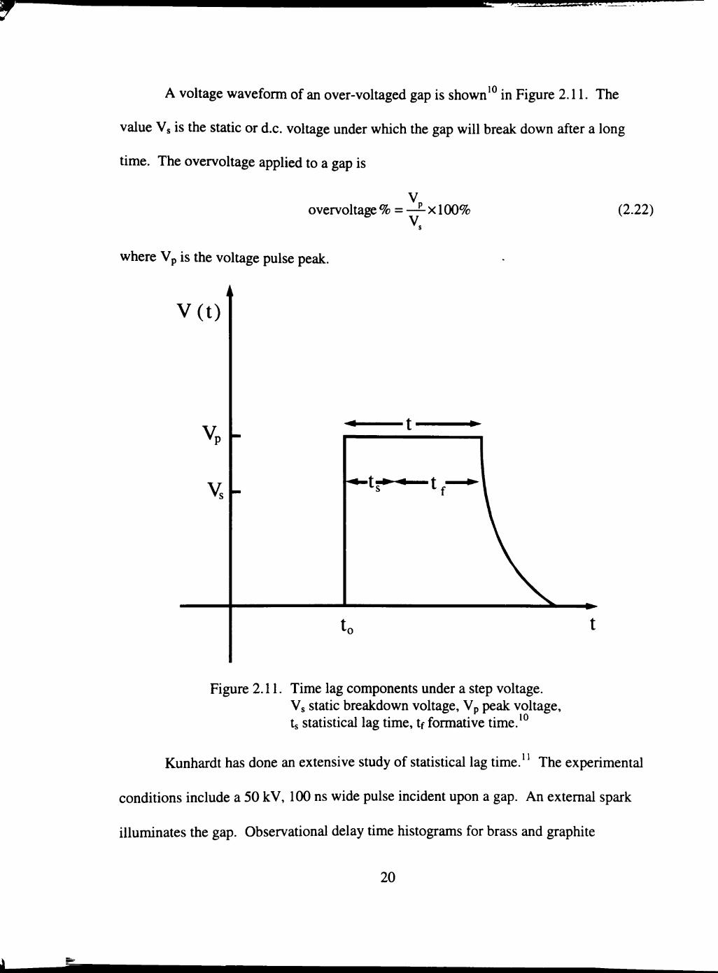
10 A voltage waveform of an over-voltaged gap is shown in Figure 2.11. The
value Vs is the static or d.c. voltage under which the gap will break down after a long
time. The overvoltage applied to a gap is
overvoltage % = —^ x 100% (2.22)
where Vp is the voltage pulse peak.
V ( t )
Vn
V. •t:
t
t
t 0 t
Figure 2.11. Time lag components under a step voltage. Vs static breakdown voltage, Vp peak voltage. ts statistical lag time, tf formative time 10
Kunhardt has done an extensive study of statistical lag time. ' The experimental
conditions include a 50 kV, 100 ns wide pulse incident upon a gap. An external spark
illuminates the gap. Observational delay time histograms for brass and graphite
20
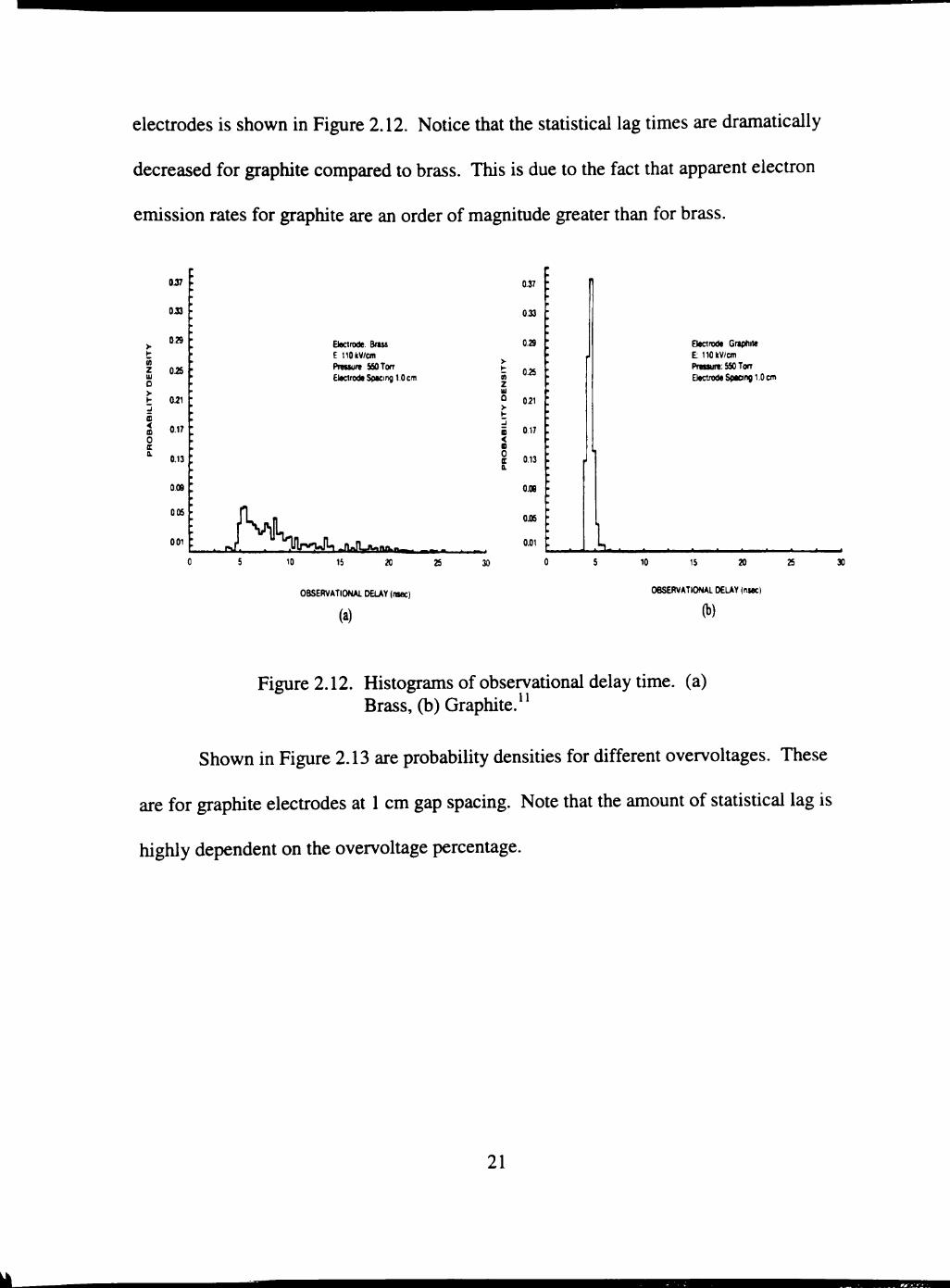
electrodes is shown in Figure 2.12. Notice that the statistical lag times are dramatically
decreased for graphite compared to brass. This is due to the fact that apparent electron
emission rates for graphite are an order of magnimde greater than for brass.
> U z 0 >
o < ffi 0 c a
0J7
0J3
029
OiS
071
0.17
0.13
OOS
005
001 t
Electrode. Brau E nOkV/cm Preuure SSOTorr Electrode Spacing 1.0 cm
J^^UxJU JlnPj^nflina 20
OBSERVATIONAL DELAY (rsecl
(a)
t-
z UI 0 >• t-
0.37
033
0i9
OiS
021 t
017 ; < B C 013 0.
o.oe
Oi)5
0.01
30 I
Electrode Graphite E: nOkV/cm Pressutc: S50 Torr Electrode Spaang 1.0 cm
10 15 20
OBSERVATIONAL DELAY (ruec)
(b)
X
Figure 2.12. Histograms of observational delay time, (a) Brass, (b) Graphite. 11
Shown in Figure 2.13 are probability densities for different overvoltages. These
are for graphite electrodes at 1 cm gap spacing. Note that the amount of statistical lag is
highly dependent on the overvoltage percentage.
21
^mm

>
W
z UJ
o > m < m 0 E
I
Gap Spacing: 1cm
Pressure: SSOTorr
% Overvoltage: 390%
X
10 15 20 0 5
OBSERVATIONAL DELAY (nsec)
Gap Spacing 1cm
Pressure 1050 Torr
% Overvoltage 200%
JUU.
10 15 20
z Ui Q >
< m 0 d Q.
Gap Spacing: 1cm
Pressure: 750 Torr
% Overvoltage: 280%
Gap Spacing: 1cm
Pressure 1350 Torr
% Overvollage 150%
. V ^ ^ ^ I V ^ 10 15 20 0 5
OBSERVATIONAL DELAY (nsec)
10 15 20
Figure 2.13. Histograms of observational delay time for various overvoltages.''
Liquid Dielectric Breakdown
Unlike electrical gas breakdown, the mechanics of liquid breakdown is not as well
established. Two general theories of liquid breakdown exist.'° One is an extension of
gas breakdown in which avalanche ionization caused by electron collision is the main
process. The electrons are introduced into the liquid gap from the cathode by either field
22

emission or field enhanced thermionic emission. This type of breakdown is reserved for
liquids of high purity.
The other theory of liquid breakdown is derived from the presence of foreign
particles in the liquid dielectric. These particles with radii, r, and permittivity, e, will
become polarized upon application of an E-field and a force will be applied , given by
F = r ' - ^ - = ^ E ( V E ) . (2.23)
For particles with e > £0, this force will cause these particles to move to the region
of highest field strength, which is the uniform gap. These particles in the gap will
enhance field lines at the surface causing perturbations in the uniform field. The
perturbations will influence particles to align in a bridge across the gap. This bridge will
enhance the entire field to a point to allow breakdown to occur.
Other types of mechanisms leading to breakdown include cavity breakdown due
to gas bubbles and electroconvection and electrohydrodynamic effects. Recall that the
breakdown formative times of interest are primarily in the nanosecond regime. It is
apparent that most of these theories require formative times of much longer periods, with
the exception being the gas breakdown extension.
J.C. Martin has collected much empirical data on liquid breakdown.'" One
particular set of data consists of propagation velocities of high voltage streamers in
several liquids. The experiments were conducted using a sphere-point electrode semp
with gap voltages up to 1.3 MV. Liquids tested include transformer oil, carbon
tetrachloride, glycerine, and deionized water.
23

The empirical expression resulting from this data relates streamer velocity to gap
voltage. The general expression is
v = kV°, (2.25)
where v is the mean streamer velocity, V is the gap voltage, and k and n are constants
dependent on the liquid dielectric. As an example, for positive polarity voltage in
transformer oil the streamer velocity expression is
v = (90±12)V' 75±O.I2 (2.26)
In Figure 2.14 are shown the plotted results for streamer velocity versus gap
voltage in transformer oil for both positive and negative polarity.
10& • f ' • » 1 ' T - T
1 100 KV
' •• ^
100
1 MV
Voltage
(a)
-5- 10
i >
1 I I I I I I I
1 100 KV
Vottage
(b)
• ••
1 MV
Figure 2.14. Streamer velocity in transformer oil. (a) positive polarity, (b) negative polarity. '
24
•«BB
1 1
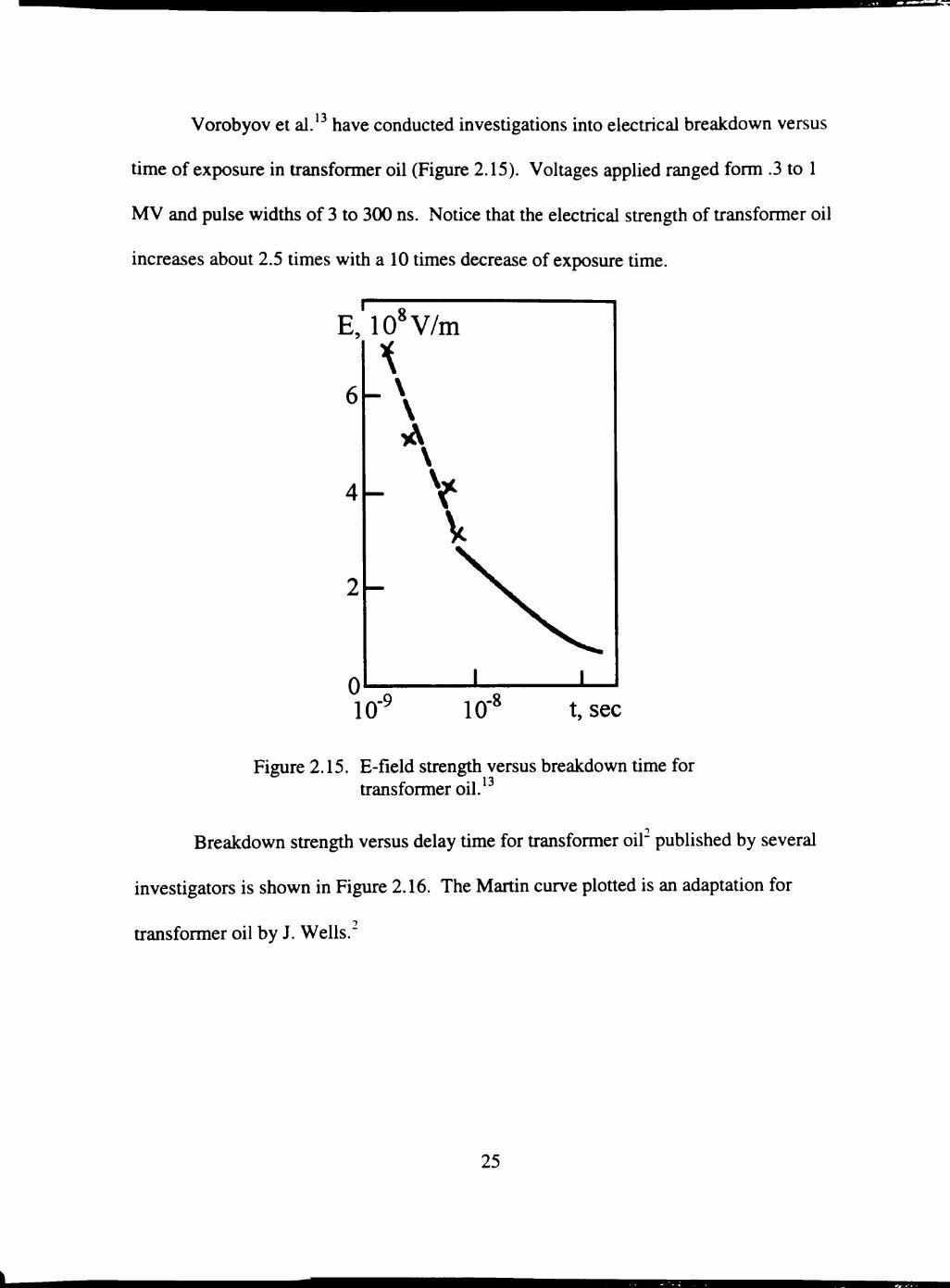
Vorobyov et al. have conducted investigations into electrical breakdown versus
time of exposure in transformer oil (Figure 2.15). Voltages applied ranged form .3 to 1
MV and pulse widths of 3 to 3(X) ns. Notice that the electrical strength of transformer oil
increases about 2.5 times with a 10 times decrease of exposure time.
t, sec
Figure 2.15. E-field strength versus breakdown time for transformer oil, 13
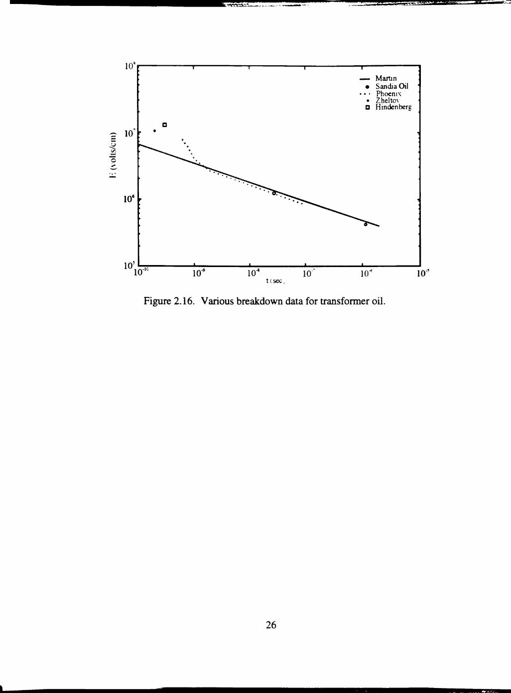
Breakdown strength versus delay time for transformer oil" published by several
investigators is shown in Figure 2.16. The Martin curve plotted is an adaptation for
transformer oil by J. Wells."
25
3 = 3 ^s
loV I -— Martin
e Sandia Oil • • • Phoenix
• Zhelto\ a Hindenbere
- 10
10'
10' 10
•10 10 10^ 10
t(sec, 10" 10'
Figure 2.16. Various breakdown data for transformer oil.
26
^sn
CHAPTER ffl
EXPERIMENTAL SETUP
Introduction
The objective to be met by the experimental semp is to investigate electrical
breakdown of liquids and gases at pressures greater than 100 atm. Breakdown time
lengths to be observed range from 500 ps to 5 ns. This required a source to supply a pulse
to a test gap area with a risetime as low as 4(X) ps. Peak electric field strengths required
at these breakdown times are as high as 7 MV/cm. Hence, for a uniform gap length of 1
mm the required voltage of the incident pulse is 100 kV.
SEF-303A Nanosecond Pulser
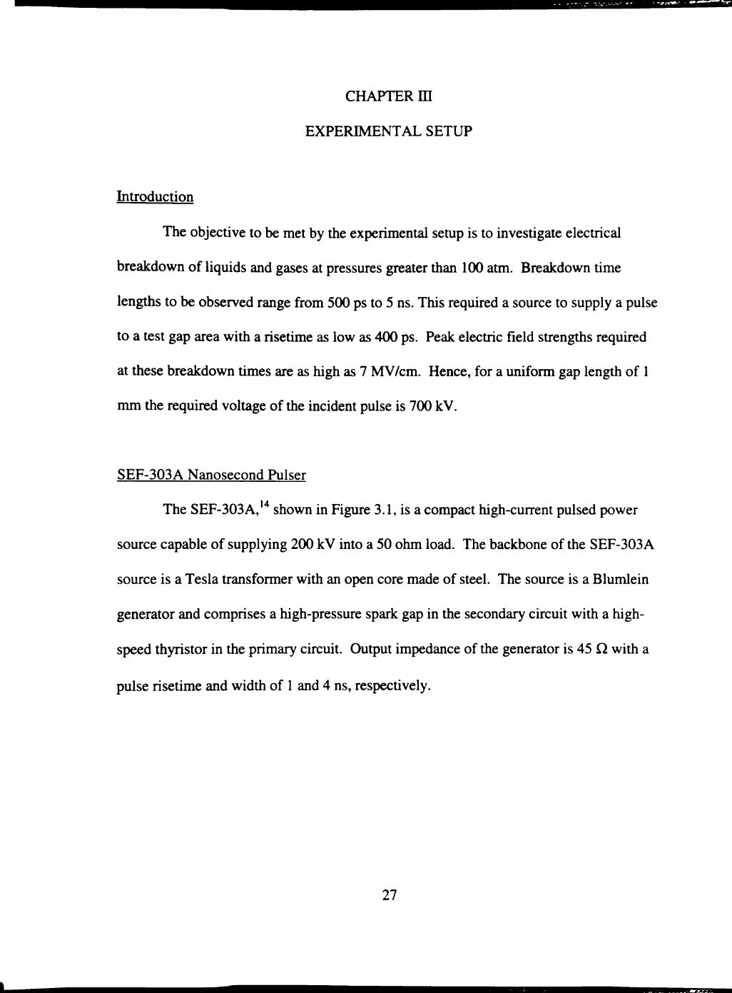
The SEF-303A, '* shown in Figure 3.1, is a compact high-current pulsed power
source capable of supplying 200 kV into a 50 ohm load. The backbone of the SEF-303 A
source is a Tesla transformer with an open core made of steel. The source is a Blumlein
generator and comprises a high-pressure spark gap in the secondary circuit with a high
speed thyristor in the primary circuit. Output impedance of the generator is 45 Q with a
pulse risetime and width of 1 and 4 ns, respectively.
27
rr r'" T
S2<S-
Sl (1-5
Figure 3.1. SEF-303A compact pulsed power source: 1-2, primary and secondary windings; 3-4, external and intemal parts of the open core; 5, spark gap switch; 6, load (e.g., e-beam or x-ray mbe); 7-8, capacitor dividers; A1-A4,
lifiers; D, driver; timers; B1-B4, pulsed amph S1-S2, output sync pulses.
The compactness of the SEF-303 A is derived from the fact that the voltage across
the primary winding is held to a relatively low value (450-5(X) V). The low primary
voltage is possible by use of a high-speed thyristor (10 kA, 0.9 kV, di/dt = 5 kA/ s) which
acts as the primary switch.
Typical operation of the SEF-303A is as follows. A 5(X) V pulse is applied across
the primary pulse transformer by way of the high voltage thyristor. The secondary
winding and Blumlein generator are charged to 150 kV in 5 }xsec (see Figure 3.2). At 5
fxsec the spark gap breaks down. When the spark gap is shorted, voltage pulses are
launched down each branch of the Blumlein, each being at an opposite polarity of the
charging voltage and at half the magnimde. These pulses combine at the output of the
pulser to form a voltage pulse of-150 kV, 4 ns wide, and 1 ns risetime into a matched
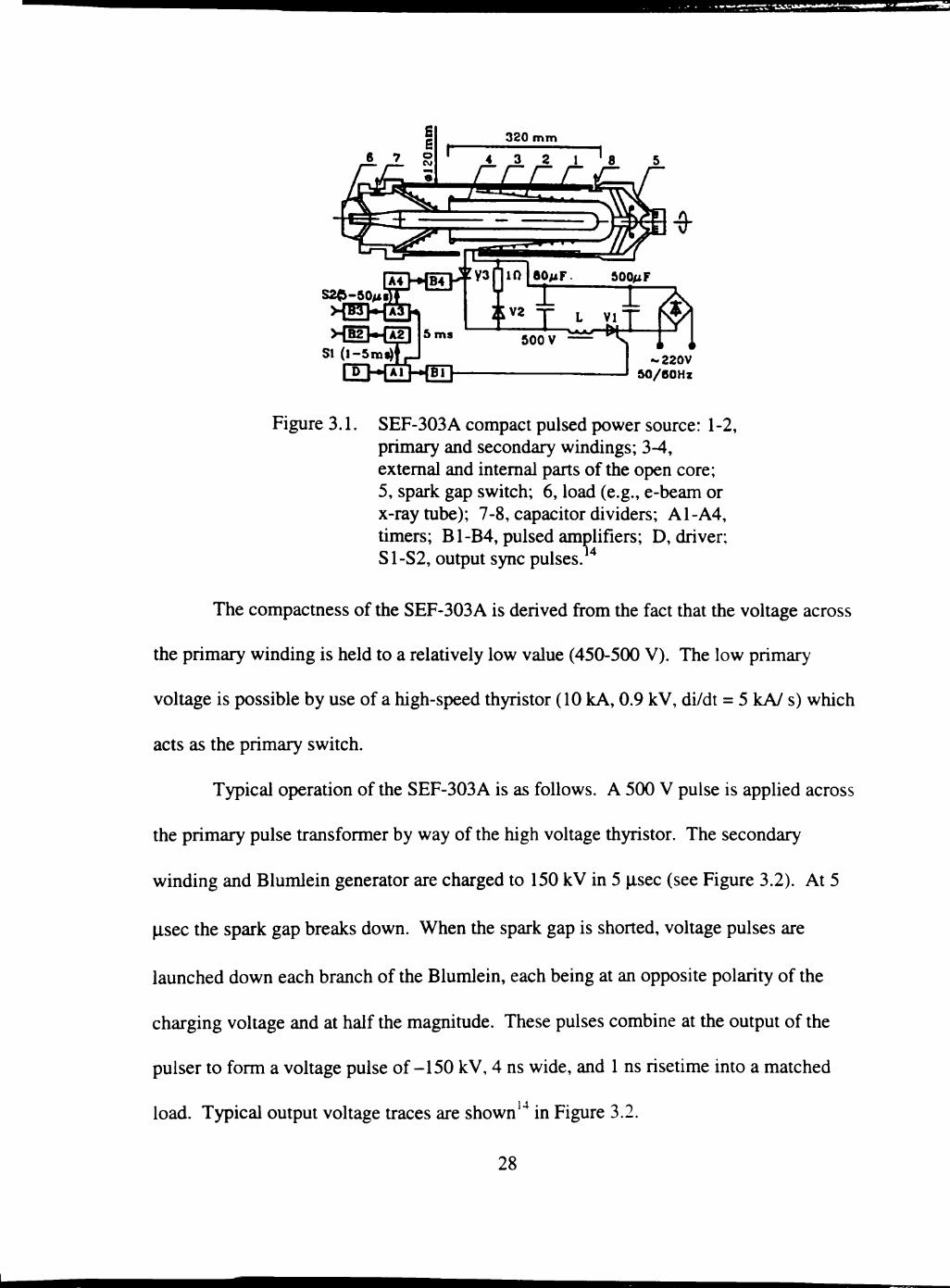
14 load. Typical output voltage traces are shown in Figure 3.2
28
^g^B^^
Figure 3.2. Traces of charging voltage of the forming line, (A), and of the output voltage at different load resistances (B refers to 50 ohm, C to 150 ohm).'^
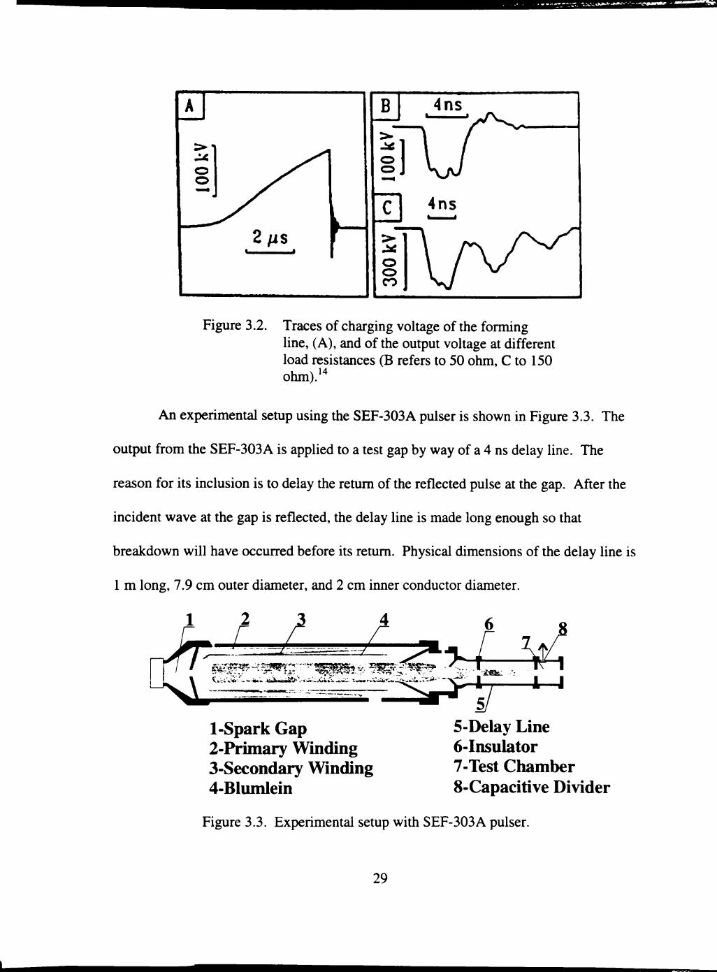
An experimental semp using the SEF-303 A pulser is shown in Figure 3.3. The
output from the SEF-303 A is applied to a test gap by way of a 4 ns delay line. The
reason for its inclusion is to delay the retum of the reflected pulse at the gap. After the
incident wave at the gap is reflected, the delay line is made long enough so that
breakdown will have occurred before its remm. Physical dimensions of the delay line is
1 m long, 7.9 cm outer diameter, and 2 cm inner conductor diameter.
A
1-Spark Gap 2-Primary Winding 3-Secondary Winding 4-Blumlein
5-Delay Line 6-Insulator 7-Test Chamber 8-Capacitive Divider
Figure 3.3. Experimental setup with SEF-303 A pulser.
29
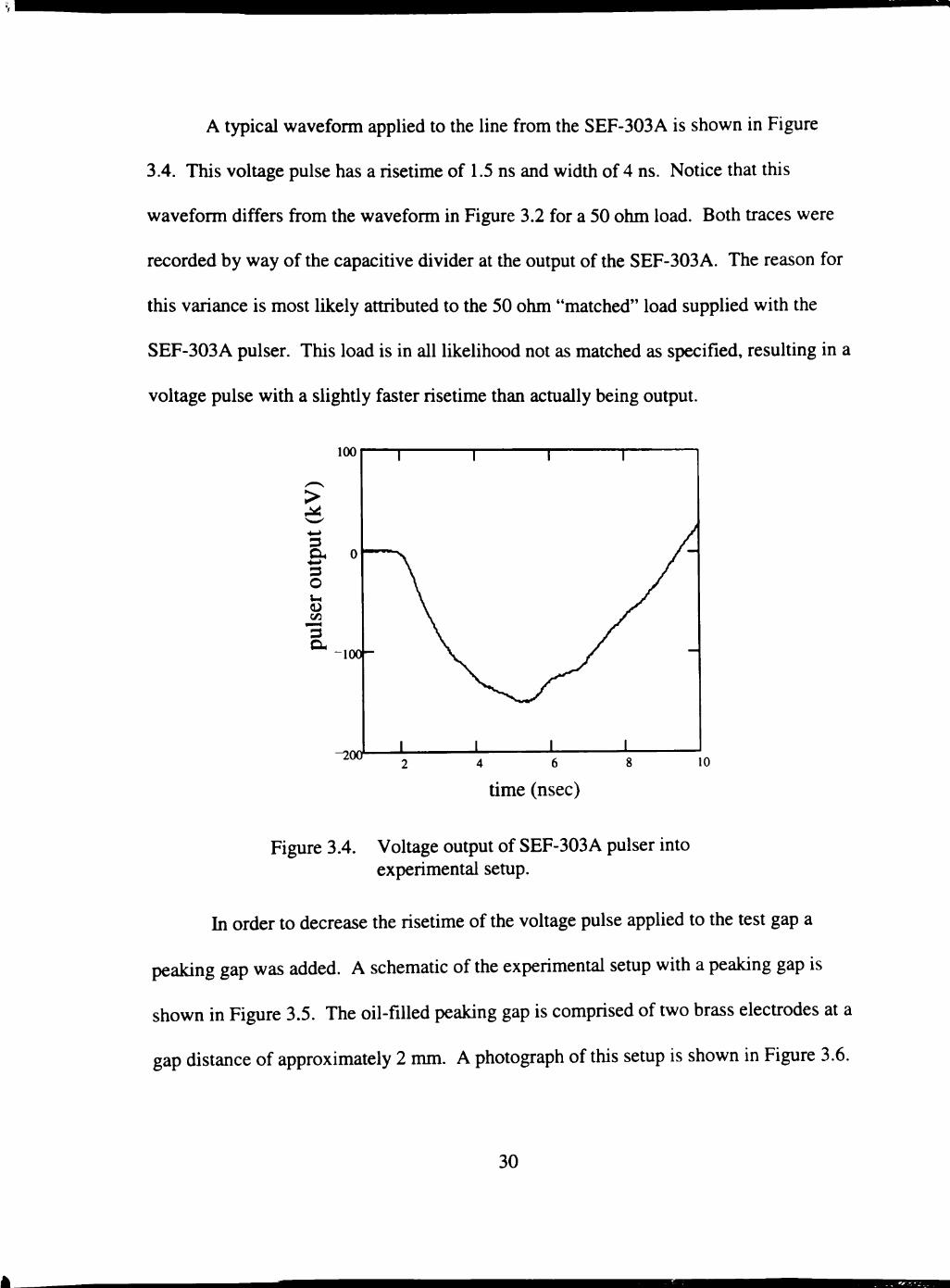
A typical waveform applied to the line from the SEF-303A is shown in Figure
3.4. This voltage pulse has a risetime of 1.5 ns and width of 4 ns. Notice that this
waveform differs from the waveform in Figure 3.2 for a 50 ohm load. Both traces were
recorded by way of the capacitive divider at the output of the SEF-303 A. The reason for
this variance is most likely attributed to the 50 ohm "matched" load supplied with the
SEF-303A pulser. This load is in all likelihood not as matched as specified, resulting in a
voltage pulse with a slightiy faster risetime than acmally being output.
>
3
3 O
(/J
a.
^ O t f
time (nsec)
Figure 3.4. Voltage output of SEF-303 A pulser into experimental semp.
In order to decrease the risetime of the voltage pulse applied to the test gap a
peaking gap was added. A schematic of the experimental semp with a peaking gap is
shown in Figure 3.5. The oil-filled peaking gap is comprised of two brass electrodes at a
gap distance of approximately 2 mm. A photograph of this setup is shown in Figure 3.6.
30

1 r
i Z 6 2; ^
1-Spark Gap 2-Primary Winding 3-Secondary Winding 4-Blumlein
I—I
5-Peaking Gap 6-Insulator 7-Test Chamber 8-Capacitive Divider
Figure 3.5. Experimental semp of SEF-303 A with peaking gap.
Figure 3.6. Photograph of the SEF-303A with peaking gap experimental semp.
A comparison of the incident voltage to an open load between the SEF-303A with
and without the peaking gap is shown in Figure 3.7. By including the peaking gap the
risetime is decreased from 1.5 ns to approximately 400 ps. Notice that the pulsewidth
and voltage magnimde remain essentially unchanged. The pre-pulse voltage in the
peaking gap waveform is a result of capactive charge across the oil-filled peaking gap.
31

BWria ^ £ 3
100
- 300 -
-400
A^ j-« ' . ^ - .
•f
with peaking gi
\nthout paaldng gap,
tinie(ns)
Figure 3.7. Gap voltages from the SEF-303A with and without peaking gap.
Marx Bank Driven PEL Pulser
The second setup is a Marx bank driven pulse forming line (PEL) capable of
delivering a 700 kV, 400 ps risetime, 3 ns wide pulse to an open test gap. A diagram of
the pulser is shown in Figure 3.8. The higher voltage allowed for a larger test gap length
thereby minimizing electrode surface effects. A photograph of this setup is shown in
Figure 3.9.
50 kV power pack 3 stage Marx bank Peaking gap Testing gap
-IHHHNHflHHHHHH ^ ^
Lexan feedthrough
Pulse forming line
Knei^.
\
T
Shorting gap
I I
Figure 3.8. Marx bank driven PEL subnanosecond pulser.
32
« « ^
Figure 3.9. Photograph of Marx bank driven PEL pulser experimental semp.
The Marx bank used was originally constructed to smdy the effects of the low
earth orbit (LEO) environment on high voltage insulators. ^ Therefore, the Marx was
originally designed to output a 500 kV pulse with a 1 p.sec risetime and an exponential
decay with a time constant -10 |xsec. The bank was originally a 10 stage Marx with a
maximum charge voltage of 50 kV per stage. The switches are spark gaps made from 2.4
cm radius brass electrodes with a 3 mm gap. The entire circuit is inserted into a 20 cm
diameter steel pressure mbe, which is back-filled and pressurized with a 50/50 mixture of
dry N2 and SF6 during operation. Gas pressure is typically 50 PSI above atmosphere.
The output voltage of the Marx can be varied by either changing the spark gap lengths or
gas pressure. The tube provides a ground retum path as well as an EMI shield for the
Marx bank, while the gas mixmre acts as an insulator.
The Marx bank originally had a 3 kQ lumped resistor at the output to the test gap.
This resistor provided the desired overdamped response. For the subnanosecond pulser
in Figure 3.8, this resistor was removed allowing the Marx to output an underdamped
response. In addition the number of stages was increased from 10 to 13. This was
motivated by the increased voltage requirement.
33
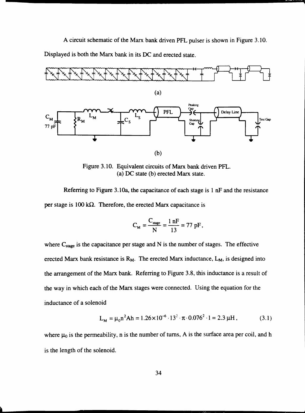
A circuit schematic of the Marx bank driven PEL pulser is shown in Figure 3.10.
Displayed is both the Marx bank in its DC and erected state.
• " " K * ' " I x * ^ ^ >•.<.'- T '" U ' " K " ' I k . ' " I k ' " I k — I k — iv""" )C >"» <v i j j ) ( • n J •
N,\r,.sr...NT• .ST \r \r..xr ^J^M M' \ ' ' T I I TI \ J ,mm Tt . . . H . . . II . . . •» . . . II . . . M . . . M M - - „ M ^ -^ M - - . M . . . N ] j | I I I I i
(a)
77 pF
rY>nr\_yC-
"RM " ^ _Lc ^VM;) ^^ h
F^aldng Gap
Shorting Gap \ 1 /
/TV
X j Delay Line j —
Test Gap
vl/ /TV
(b)
Figure 3.10. Equivalent circuits of Marx bank driven PITL. (a) DC state (b) erected Marx state.
Referring to Figure 3.10a, the capacitance of each stage is 1 nF and the resistance
per stage is 100 kQ. Therefore, the erected Marx capacitance is
C.,=S2IL = iilF = 77pF, 'M N 13
where Cstage is the capacitance per stage and N is the number of stages. The effective
erected Marx bank resistance is RM- The erected Marx inductance, LM, is designed into
the arrangement of the Marx bank. Referring to Figure 3.8, this inductance is a result of
the way in which each of the Marx stages were connected. Using the equation for the
inductance of a solenoid
L , = lon'Ah = 1.26x10"^ 13' 7c0.076^ • 1 = 2.3 iH, (3.1)
where Ho is the permeability, n is the number of mms, A is the surface area per coil, and h
is the length of the solenoid.
34
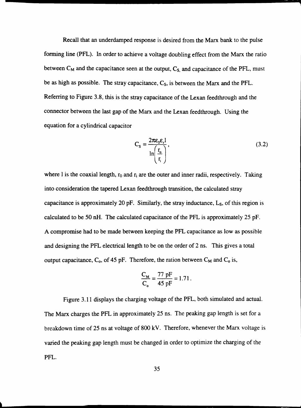
Recall that an underdamped response is desired from the Marx bank to the pulse
forming line (PEL). In order to achieve a voltage doubling effect from the Marx the ratio
between CM and the capacitance seen at the output, Cs, and capacitance of the PEL, must
be as high as possible. The stray capacitance, Cs, is between the Marx and the PEL.
Referring to Figure 3.8, this is the stray capacitance of the Lexan feedthrough and the
coimector between the last gap of the Marx and the Lexan feedthrough. Using the
equation for a cylindrical capacitor
27tene,l
In C s = - 7 H ' (3.2)
To
where 1 is the coaxial length, ro and ri are the outer and inner radii, respectively. Taking
into consideration the tapered Lexan feedthrough transition, the calculated stray
capacitance is approximately 20 pF. Similarly, the stray inductance, Ls, of this region is
calculated to be 50 nH. The calculated capacitance of the PFT- is approximately 25 pF.
A compromise had to be made between keeping the PEL capacitance as low as possible
and designing the PEL electrical length to be on the order of 2 ns. This gives a total
output capacitance, Co, of 45 pF. Therefore, the ration between CM and Co is.
Co 45 pF
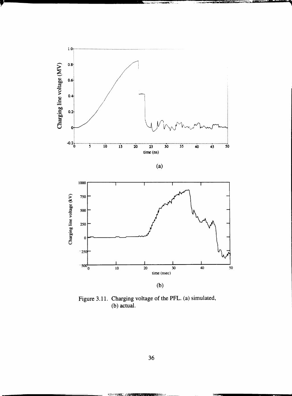
Figure 3.11 displays the charging voltage of the PEL, both simulated and actual.
The Marx charges the PEL in approximately 25 ns. The peaking gap length is set for a
breakdown time of 25 ns at voltage of 8(X) kV. Therefore, whenever the Marx voltage is
varied the peaking gap length must be changed in order to optimize the charging of the
PEL.
35
'
• I 111'. ' .» • n j i L i j ^ e t g r m ; m r r itm
l.Or
>
B "o > C
c
t s: U
5 10 15 20 25 30 35 40 45 time (ns)
'50
(a)
1000
>
u 00 B > u c 00 c '5b x: U
10 20 30 time (nsec)
40 50
(b)
Figure 3.11. Charging voltage of the PEL. (a) simulated, (b) actual.
36
tixy^'-
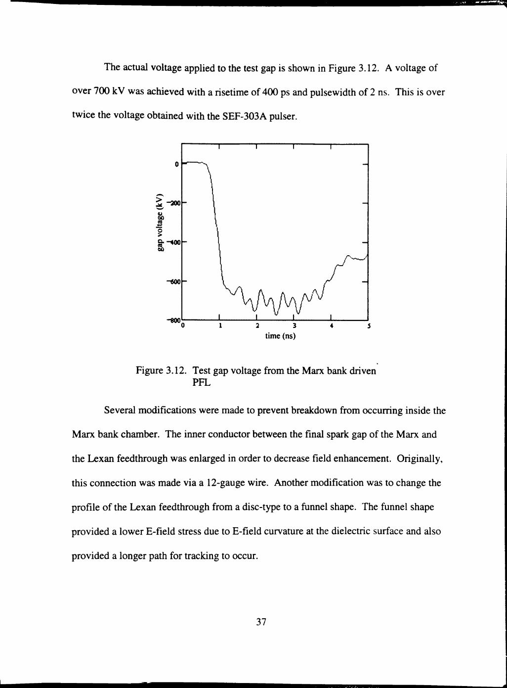
The acmal voltage applied to the test gap is shown in Figure 3.12. A voltage of
over 700 kV was achieved with a risetime of 400 ps and pulsewidth of 2 ns. This is over
twice the voltage obtained with the SEF-303A pulser.
Figure 3.12. Test gap voltage from the Marx bank driven PEL
Several modifications were made to prevent breakdown from occurring inside the
Marx bank chamber. The inner conductor between the final spark gap of the Marx and
the Lexan feedthrough was enlarged in order to decrease field enhancement. Originally,
this connection was made via a 12-gauge wire. Another modification was to change the
profile of the Lexan feedthrough from a disc-type to a funnel shape. The funnel shape
provided a lower E-field stress due to E-field curvature at the dielectric surface and also
provided a longer path for tracking to occur.
37
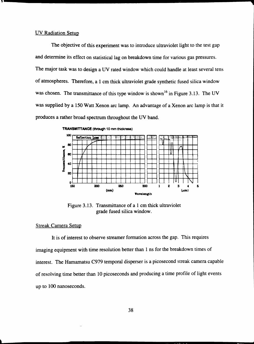
UV Radiation Setup
The objective of this experiment was to introduce ultraviolet light to the test gap
and determine its effect on statistical lag on breakdown time for various gas pressures.
The major task was to design a UV rated window which could handle at least several tens
of atmospheres. Therefore, a 1 cm thick ultraviolet grade synthetic fused silica window
was chosen. The transmittance of this type window is shown' in Figure 3.13. The UV
was supplied by a 150 Watt Xenon arc lamp. An advantage of a Xenon arc lamp is that it
produces a rather broad spectrum throughout the UV band.
TRANSMriTANCE (through 10 mm thickness)
100
80
60
40
20
• 'Mw^n.Um.x rrrr.
J /
/
' : , ; • - ' • : ; - • - .
•S' 1 yA-'. •:•':
.•.\fti iy«'.«
,1 M
u
A
i;;.'-'
I \ ,,
[\
i
160 200 260 (nm)
300
Wavelan^h
3 4
Figure 3.13. Transmittance of a 1 cm thick ultraviolet grade fused silica window.
Streak Camera Setup
It is of interest to observe streamer formation across the gap. This requires
imaging equipment with time resolution better than 1 ns for the breakdown times of
interest. The Hamamatsu C979 temporal disperser is a picosecond streak camera capable
of resolving time better than 10 picoseconds and producing a time profile of light events
up to 1(X) nanoseconds.
38
n

The temporal disperser principle of operation' is as follows (see Figure 3.14).
Light incident on the input slit is focused onto the photocathode. The incident photons
are converted to electrons and accelerated from the photocathode toward the sweeping
electrodes via an accelerating mesh. Voltage across the sweeping electrodes is
synchronized with the arriving electrons to decrease linearly in time, which sweeps the
electrons from top down during the streak operation. The swept electrons are projected
onto a micro-channel-plate where electron multiplication is accomplished. These
electrons exit the micro-channel-plate and bombard the phosphor screen, and are
converted into an optical image.
Trigger •
Incident Light
Photocathode
Sweep Generator
_ y uectrode Sweeping Electrode
MicroChannel-Plate Phosphor
Screen
Accel. Mesh
^
Figure 3.14. Schemetic of the Hamamatsu streak camera.
Figure 3.15 shows a schematic of the experimental semp incorporating the streak
camera. When the SEF-303A pulser is triggered a voltage is output from the
microsecond detector several microseconds before the SEF-303A output pulse is applied
to the test gap. This detector voltage is delayed by the delay generator and output to the
trigger input of the streak camera. The streak camera requires a trigger approximately 10
to 20 ns before the event to be recorded. The gap is imaged on the slit of the camera via a
39
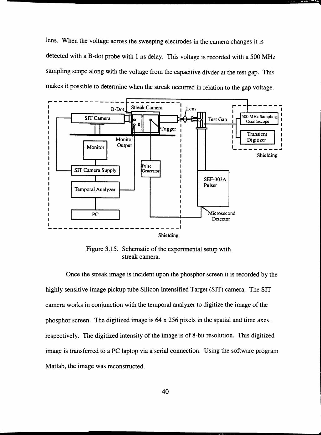
lens. When the voltage across the sweeping electrodes in the camera changes it is
detected with a B-dot probe with 1 ns delay. This voltage is recorded with a 500 MHz
sampling scope along with the voltage from the capacitive divder at the test gap. This
makes it possible to determine when the streak occurred in relation to the gap voltage.
B-Dot. Streak Camera ns
SIT Camera
Monitor
I
Monitor Output
SIT Camera Supply
Temporal Analyzer
fTngger
Pulse Generator
PC
Test Gap • f 500 MHz Sampling
Oscilloscope
Transient Digitizer
Shielding
SEF-303A Pulser
FT Microsecond Detector
Shielding
Figure 3.15. Schematic of the experimental semp with streak camera.
Once the streak image is incident upon the phosphor screen it is recorded by the
highly sensitive image pickup mbe Silicon Intensified Target (SIT) camera. The SIT
camera works in conjunction with the temporal analyzer to digitize the image of the
phosphor screen. The digitized image is 64 x 256 pixels in the spatial and time axes,
respectively. The digitized intensity of the image is of 8-bit resolution. This digitized
image is transferred to a PC laptop via a serial connection. Using the software program
Matlab, the image was reconstructed.
40
VWMSMkXW^'v.i gsBc: M i l l " ' ' '"ii"T'ar""
Test Gap
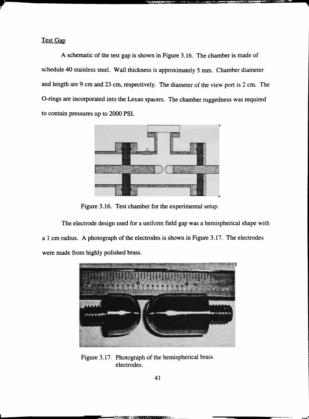
A schematic of the test gap is shown in Figure 3.16. The chamber is made of
schedule 40 stainless steel. Wall thickness is approximately 5 mm. Chamber diameter
and length are 9 cm and 23 cm, respectively. The diameter of the view port is 2 cm. The
O-rings are incorporated into the Lexan spacers. The chamber mggedness was required
to contain pressures up to 2000 PSI.
'g."*1tf» '-:
fe.WWigJW'W^ <;;jf..*.w..jjjmj.\i-ja'."i.va«..atMWCT?T
Figure 3.16. Test chamber for the experimental setup.
The electrode design used for a uniform field gap was a hemispherical shape with
a 1 cm radius. A photograph of the electrodes is shown in Figure 3.17. The electrodes
were made from highly polished brass.
Figure 3.17. Photograph of the hemispherical brass electrodes.
41
"m
I I I I l ^ p — T -
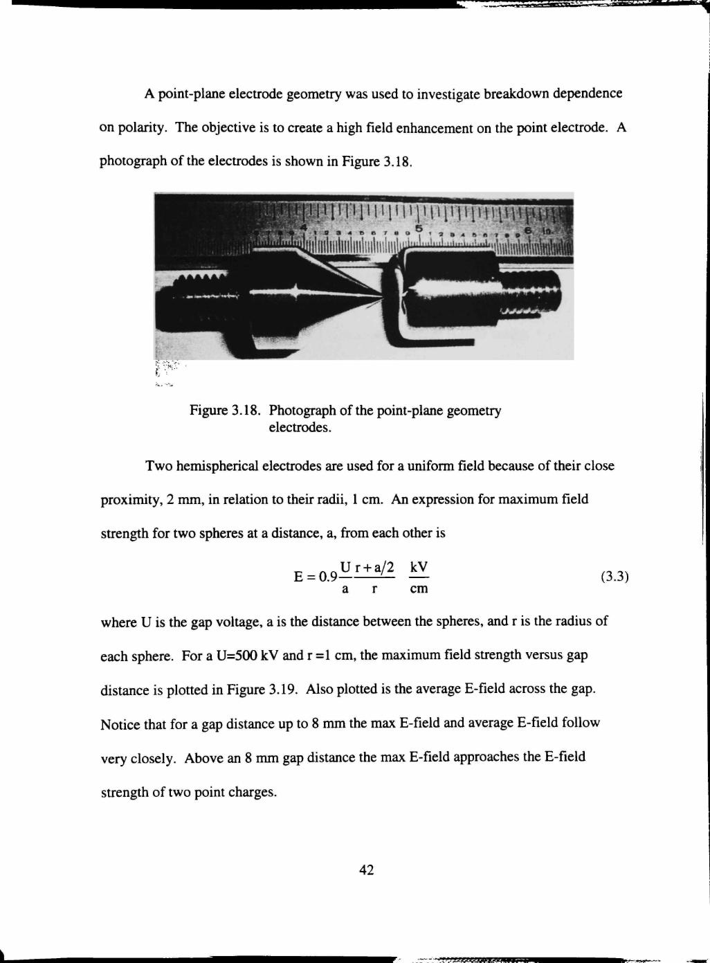
A point-plane electrode geometry was used to investigate breakdown dependence
on polarity. The objective is to create a high field enhancement on the point electrode. A
photograph of the electrodes is shown in Figure 3.18.
Figure 3.18. Photograph of the point-plane geometry electrodes.
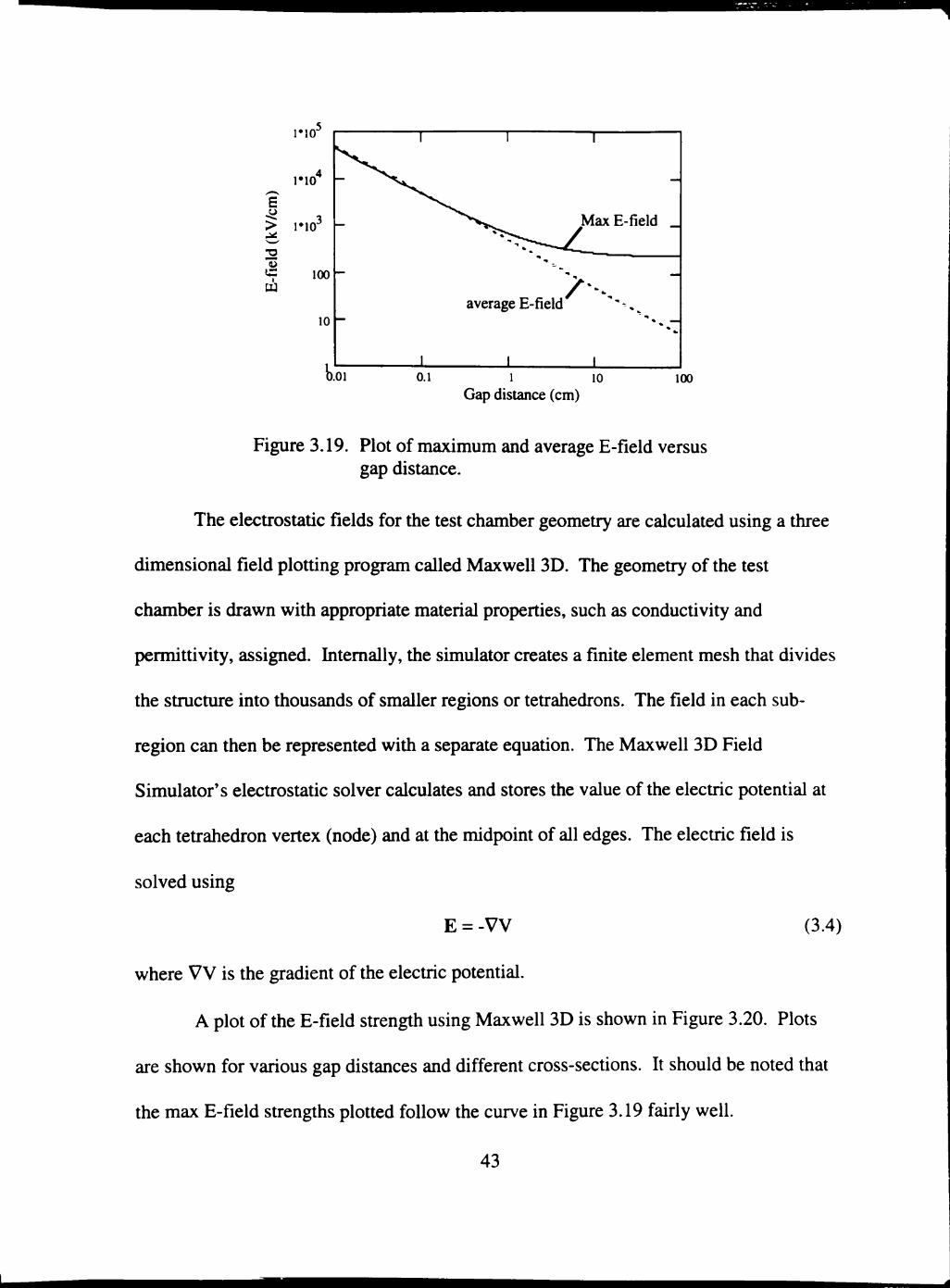
Two hemispherical electrodes are used for a uniform field because of their close
proximity, 2 mm, in relation to their radii, 1 cm. An expression for maximum field
strength for two spheres at a distance, a, from each other is
E = 0.9 Ur-Ha/2 kV
(3.3) cm
where U is the gap voltage, a is the distance between the spheres, and r is the radius of
each sphere. For a U=500 kV and r =1 cm, the maximum field strength versus gap
distance is plotted in Figure 3.19. Also plotted is the average E-field across the gap.
Notice that for a gap distance up to 8 mm the max E-field and average E-field follow
very closely. Above an 8 mm gap distance the max E-field approaches the E-field
strength of two point charges.
42
^
10
1.01
Max E-field _
average E-field
0.1 1 10
Gap distance (cm) 100
Figure 3.19. Plot of maximum and average E-field versus gap distance.
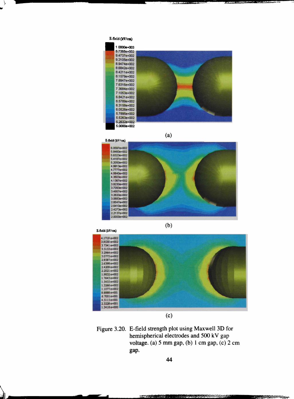
The electrostatic fields for the test chamber geometry are calculated using a three
dimensional field plotting program called Maxwell 3D. The geometry of the test
chamber is drawn with appropriate material properties, such as conductivity and
permittivity, assigned. Internally, the simulator creates a finite element mesh that divides
the strucmre into thousands of smaller regions or tetrahedrons. The field in each sub-
region can then be represented with a separate equation. The Maxwell 3D Field
Simulator's electrostatic solver calculates and stores the value of the electric potential at
each tetrahedron vertex (node) and at the midpoint of all edges. The electric field is
solved using
E = -VV (3.4)
where W is the gradient of the electric potential.
A plot of the E-field strength using Maxwell 3D is shown in Figure 3.20. Plots
are shown for various gap distances and different cross-sections. It should be noted that
the max E-field strengths plotted follow the curve in Figure 3.19 fairly well.
43
•^IHS^BE "H aa ^s
Enfield (kV/cm)
1000064003 9 7368e+002 9 4737e+Q02 9 2105e+002 8 9474ef002
, e.6842e>002 8 4211e-)-002 81579e*G02
I 7 8947e+002 7 6316e*002
j 7 3684e+002 71053e*002 8.8421 e+002 6.5789e+002 6.3158e*002 6.G528e+002 5.7895e*G02 5.526364002 5263264002 5.000064002
E-fieldftV/cnO
6.05976+002 5 846064002 5 6323e+002 5 4187e+002
! 5 205064002 I 4.991304002 4.777764002 4.564064002 4.350364002 4.136764002 3.923064002 3.709364002 3.495764002 3.282064002 3.068364002 2.854764002 2.641064002 2.427364002 2.213764002 2.W00e4002
E-field (kV/caO
14.1719 64002 13.9230 64002 13 734164002 3 515364002 "3 2964 64002 13.077564002 12.8587 6+002 12.6398 e+002 12.420964002 12.20216+002
1.98326+002 11 76436+002
154556+002 132666+002
11 1077 6+002 18 88886+001 16.70016+001 14 51156+001 13 3228 6+001
1.3418 6+000
(a)
(b)
Figure 3.20. E-field strength plot using Maxwell 3D for hemispherical electrodes and 5(X) kV gap voltage, (a) 5 mm gap, (b) 1 cm gap, (c) 2 cm gap.
44
I u m pjin^w! is^mAA^u-.iy^. '._^is_^ -lyiLia
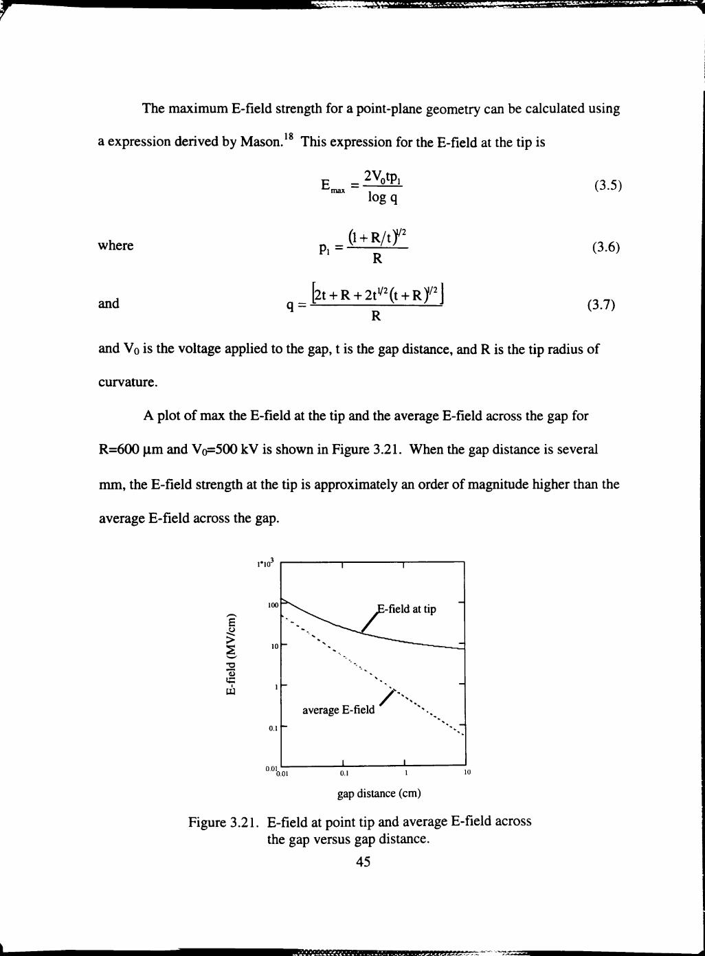
The maximum E-field strength for a point-plane geometry can be calculated using
18 a expression derived by Mason. This expression for the E-field at the tip is
E _ = max
_ 2Votp, logq
(3.5)
where O^R/tf (3.6)
and q = [2t-HR-h2t'/^(t-HRf j
R (3.7)
and Vo is the voltage applied to the gap, t is the gap distance, and R is the tip radius of
curvamre.
A plot of max the E-field at the tip and the average E-field across the gap for
R=600 |im and Vo=500 kV is shown in Figure 3.21. When the gap distance is several
mm, the E-field strength at the tip is approximately an order of magnimde higher than the
average E-field across the gap.
rio^
100 -field at tip E o >
0.1
0,01
average E-field / ..
0.01 0.1 10
gap distance (cm)
Figure 3.21. E-field at point tip and average E-field across the gap versus gap distance.
45
WQgfiWWaaHllilllUIMllJM 'KMlfJMJL'-^^-

The electrostatic field for the test chamber with a point-plane electrode geometry
is calculated using Maxwell 3D. In Figure 3.22 are several plots for E-field su-ength at
different gap distances and cross-sections. These E-field strengths compare well with
those predicted in Figure 3.21.
Enfield (MV/cm)
1.27076+001 1.20376+001 1.13676+001 1.06986+001 1.00286+001 9.35776+000 8.68786+000 8.01796+000 7.34806+000 6.67806+000 6.00816+000 5.33826+000 4.66836+000 3.99846+000 3.32846+000 2.65856+000 1.98866+000 1.31876+000 6.48766+000 0.00006+000
Figure 3.22. E-field strength plots for test chamber with point-plane electrodes and 500 kV gap voltage, (a) 1 mm gap, (b) 2 mm gap, (c) 5 mm gap
46
mmmmm
E-ficld (MV/cm)
9.91706+000 9.39516+000 8.87316+000 8.35126+000 7.82926+000 7.30736+000 6.78536+000 6.26346+000 5.74146+000 5.2195e+000 4.69756+000 4.1756e+000 3.65366+000 3.13176+000 2.60976+000 2.08786+000 1.56586+000 1.04396+000 5.21956-001 O.OOOOe+000
Trrr Enfield (MV/cm)
2076+000 ^ ^ ^ ^ ^ ^ ^ ^ ^ ^ 6.74596+000 6.37126+000 5.99646+000 5.62166+000 5.24686+000 4.87216+000 4.49736+000 4.12256+000 3.74776+000 3.37306+000 2.99826+000 2.62346+000 2.24866+000 1.87396+000 1.49916+000 1.12436+000
7.49556-001 3.74776-001 O.OOOOe+000 ^H
(c)
Figure 3.22. Continued.
47
ZJ-'-Ci SSSSSBEEOEBB^^z
giQ^gg • ^ ^ • ^ ^ • B
CHAPTER IV
DL\GNOSTICS
Introduction
Ultrawideband pulses with their fast risetimes (-150 ps) require diagnostics with
high bandwidths (-4 GHz). The 150 ps risetime was an initial goal; however, risetimes
-400 ps were acmally achieved. The four major components of the diagnostics semp are
the high voltage divider, wide-band attenuator, wide-band cable, and the recorder. The
chosen recorder is the Tektronix SCD-5000 transient event digitizer. The analog
bandwidth of the SCD 5000 is approximately 4.5 GHz. This corresponds to recording
risetimes of
0.35 0.35
The wide-band cable used is semi-rigid with a bandwidth greater than 15 GHz. The
wide-band attenuator has a bandwidth of 8 GHz and a rated peak power of 5 kW.
High Voltage Dividers
For the measurement of high voltage pulses there are two distinct types of
attenuators to consider: a resistor divider and a capacitor divider. A schematic of a
resistor divider circuit is shown^^ in Figure 4.1. The RH refers to the high impedance
element and RL refers to the low impedance element of the resistive divider. The R<i is a
damping resistor included to attenuate the high frequency oscillation due to the stray
capacitances and residual inductance. The capacitors shown represent capacitive coupling
48
between various points on the divider. The CH refers to coupling between various points
on the divider, and Co refers to coupling between points on the divider and ground.
V; ^ ^
Figure 4.1. Equivalent circuit of a resistive divider. 19
The step response of the circuit in Figure 4.1 is shown in Figure 4.2 for a damping
resistor of zero ohms. ^ It is obvious that such a device is unsuitable for the measurement
of a signal which has significant variations on time scales shorter than about 10 |j,sec
because high frequency oscillations would be induced on the output waveform that were
not present on the input voltage. When a value of the damping resistor is increased, the
oscillations are damped, however the response time of the divider decreases. For
example, when Rd = 57 Q the oscillations are successfully damped but the response time
of the divider increases from 45 ns to 90 ns.
V(t)
tOisec)
Figure 4.2. Step response of a resistive divider with Rd = 0 Q 19
49
It is evident that a resistor divider is not adequate for the measurement of
nanosecond voltage pulses. Therefore a capacitor divider is the preferred attenuator. The
schematic of a typical capacitive divider, often used in coaxial systems, is shown in
Figure 4.3. The capacitances Ci and C2 are not lumped elements but rather stray
capacitances designed into the geometry of the system for desired values. A simplified
equivalent circuit for this type of divider is shown ^ in Figure 4.4. The impedance of the
cable is assumed to match R2.
High Voltage Electrode
_^i Line Dielectric
c
C2 I
Ground Plane y
Dielectric Sleeve*
Grounded Sleeve" I:-Cable Connectoi r ^
'Conducting Piece
Resistors
Figure 4.3. Schematic of a typical capacitive divider 20
If V,
Rl i ^ R V.
Figure 4.4. Circuit equivalent of a typical capacitive divider 19
50
t i - •.-r"~C=C=acCttSB
The calculated unit step response of the circuit in Figure 4.4 is given by
/ ^ V D \ C c,+c.
R.
R,-HR. V(t)= — ^ — ^ exp(-t/T) (4.2)
where the time constant, x, is
T = (C,-hC2(R,+R2)) (4.3)
Choosing typical values,
C2=10-*tolO-^F»C„
R, = R2=50Q,
yields a time constant of
T = 100 to 1000 ns.
A measured step response for this type of capacitive divider is shown'^ in Figure
4.5. This was a low voltage measurement with the pulse being supplied to the gas-
insulated test line through a mercury-wetted relay. The risetime of the pulse is on the
order of 1 ns which was expected from the relay. It can be seen in Figure 4.5 that
oscillations occur after 20 ns. These are not due to characteristics of the divider but
rather are due to reflections in the high voltage circuit. A second observation is that there
is significant droop in the output of the divider during the first 50 ns. The divider,
therefore, could not be used without correction for an accurate measurement of voltages
which have variations on these time scales. For measurements at these time scales,
correction by either software or hardware would be required.
51
r^rr^^^^^nw-" '' • 'vnrMUiirfiiirrim""
200 m V ^
u 00
S
3 a. "3 O
0
200 mVp-
00 S o > "3 a.
O
0
J. 10
Time (ns)
250 Time (ns)
20
Figure 4.5. Measured step response of a capacitor divider at different time scales. ^
Although the droop of a capacitive divider is an important characteristic, it is of
less importance than the risetime when measuring nanosecond wide pulses. Recall that
the time constant of this type of capacitive divider is typically between 100 and ICXX) ns.
The question then arises, what are the shortest risetimes that can be obtained from a
capacitive divider.
Risetimes on the order of a 100 ps have been recorded. The behavior of a ground
plane mounted transmission line E-field sensor, as shown in Figure 4.6, has been
21 investigated by Buchenauer and Marek. The output pulse applied to the sensor was a
52
step with a 10 volt amplitude and 45 ps risetime. Acceptable performance is achieved
only when the incident wave direction is perpendicular to the stripline axis or <p = 0°.
L'
n>^ 2a
Top View
. ^
Ground Plane
Stnpline Sensor StrpHne-to-Coax transition
Side View ielectric
Figure 4.6. A dense dielectric supported stripline E-field sensor.
Figure 4.7 shows the step response of this sensor constmcted on teflon for (p = 0**
and L' of several lengths. The mid-trace aberration diminishes with increasing L'. This
is an end effect that occurs on a dielectric strip of finite length because the electrode is
not raised to a constant potential along its length after passage of the incident wave. Net
longimdinal surface currents begin flowing near the end as the wave traverses the width
of the line, thus generating the aberrant signal at time L/Ceff, where Ceff is the effective
speed of light through the dielectric. This effect diminishes with increasing L' as
electrical conditions approach those for a infinite dielectric strip. This effect has also
been observed by the author using a similar type sensor.
53

I'lriii ir'-''-''-r' ' ' U f i r w
100 mV"
20 mV /div
-20raV 74.27 ns 1 SO ns/div 75.77 ns
Figure 4.7. Step response of the dense dielectric supported stripline E-field sensor. ^
The risetime of the strip line step response is observed to be about 130 ps. Recall
that the applied pulse risetime is 45 ps. The sensor response is altered by the dielectric.
However, to accurately maintain sub-millimeter physical height, which is necessary to
meet the high attenuation requirement, a solid dielectric must often be used.
Umbrella Probe
A variation of the strip line for a coaxial geometry is the umbrella probe.~~ A
cross-section of a coaxial line with an umbrella probe is shown in Figure 4.8. The
attenuation of such a probe can easily be calculated.
54
^S^SSSSBS^^SS^ Unilu u\i\ •! 11 iiiirii laMMiiTfriiiafc^
Inner Conductor
Line Dielectric
Outer Conductor
Umbrella Probe
50 ohm cable
Probe Dielectric, £2
Figure 4.8. Coaxial line with umbrella probe.
As a transverse electromagnetic (TEM) wave propagates along a coaxial line the
electric field intensity is directed only along the radial axis normal to the cylindrical
surface. The expression for the E-field intensity with respect to r for two concentric
conducting planes can be found easily from applying Gauss law
i: — i l l (4.4)
where ps is the surface charge density and e is the medium permittivity. The potential
difference between the inner conductor and the outer conductor of the umbrella probe is
'ab
r=a a /
= - j E , d l = -J a. r=b
\
' l y
(4.5)
where a is the inner conductor radius, b is the radius to the umbrella probe, and ei is the
permittivity of the coaxial line. Similarly, the potential difference across the umbrella
probe is found to be
55
^^hjBB I > 11 ai'w^^ A • • - -» -I II ni Tm-1»' KSsmii. i—L6Mr,nf.nBirBM

^
V.=^ln P £-2
(4.6)
where c is the radius of the outer conductor and £2 is the permittivity of the umbrella
probe dielectric.
The voltage applied to the coaxial line,Vac, is the sum of these two voltages
Vac — Vab + Vbc (4.7)
The probe attenuation is found to be
A = 'be 'be
^ i n f -1 e, In
ac v.. + v^
P^ln £2
^c^
voy £2 In + e, In
.b>
(4.8)
The probe attenuation can also be found in terms of the capacitance. The capacitance
between the inner conductor and the umbrella probe is
C , = 27ce, 1
In '-1 ^a>
w probe
P"** 27tb ' (4.9)
where Wprobe is the width of the probe and Iprobe is the length of the probe. The
capacitance between the umbrella probe and the outer conductor is
C. = 27ce.
w. probe
In ^ ^ N "probe 27jb '
(4.10)
Vbj
where both capacitance calculations neglect fringing. Inserting eqns. (4.9) and (4.10) into
eqn. (4.8) we get.
56

2n£,2 Iprobe 1 £ W
1 r p->^ 2nb C, C, A = = ^ — = •— f 4 1 n
27C£^ Iprob^ 27C£^ Vob^ — + — C . - h C , • ^ • ^
' C, ' ^P- ' «27 ib ' ^^ ' C2 '^•^'*27ib C, C2
These probes are designed to detect voltages in the Megavolt range. For coaxial
lines with radii in the cm range, an umbrella probe thickness, 6, of 10 to 100 ^m will
provide attenuation of about 1000. Another factor in determining 6 is the typical voltage
to be applied on the probe and the breakdown strength of the dielectric. Some common
dielectrics used are polyethylene and kapton.
The geometrical shape of the umbrella can be, in principle, arbitrary, but its
characteristic dimension (e.g., the radius of a round umbrella) must satisfy the condition
of quasi-steadiness. According to this condition, the time of the wave path along the
characteristic dimension must be significantiy lower than the duration, T, of the
registered pulse. For example, for a round umbrella
R « - r - , (4.12)
^Je2
where R is the umbrella radius, c is the speed of light in vacuum, and £2 is the probe
permittivity.
The advantages of the capacitive umbrella probe are the wide bandwidth due to
the inherently vanishingly small inductance from the geometry and the ability to obtain a
rough attenuation coefficient by measuring the probe capacitance and calculating from
eqn. (4.11). The upper boundary of the bandwidth (several Gigahertz) is determined by
the physical dimensions of the probe.
57
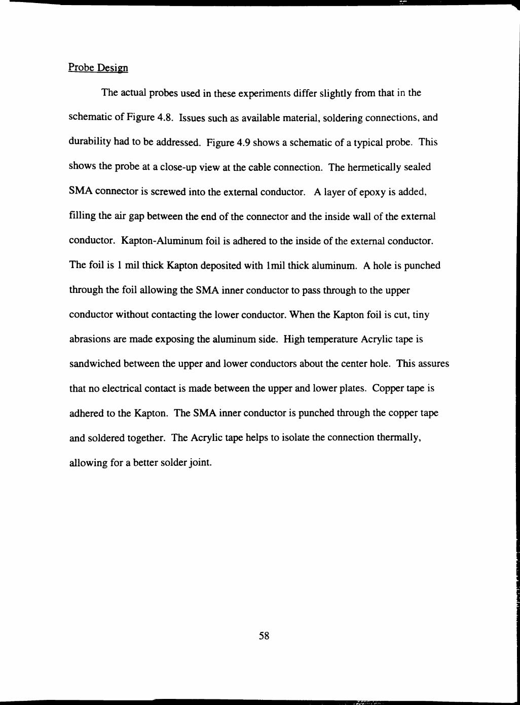
Probe Design
The acmal probes used in these experiments differ slightiy from that in the
schematic of Figure 4.8. Issues such as available material, soldering connections, and
durability had to be addressed. Figure 4.9 shows a schematic of a typical probe. This
shows the probe at a close-up view at the cable connection. The hermetically sealed
SMA coimector is screwed into the extemal conductor. A layer of epoxy is added,
filling the air gap between the end of the connector and the inside wall of the extemal
conductor. Kapton-Aluminum foil is adhered to the inside of the extemal conductor.
The foil is 1 mil thick Kapton deposited with Imil thick aluminum. A hole is punched
through the foil allowing the SMA inner conductor to pass through to the upper
conductor without contacting the lower conductor. When the Kapton foil is cut, tiny
abrasions are made exposing the aluminum side. High temperamre Acrylic tape is
sandwiched between the upper and lower conductors about the center hole. This assures
that no electrical contact is made between the upper and lower plates. Copper tape is
adhered to the Kapton. The SMA inner conductor is punched through the copper tape
and soldered together. The Acrylic tape helps to isolate the connection thermally,
allowing for a better solder joint.
58

^ ^
Copper tape
Kapton
^ :/^//////>'.V^V>'^^-'/T'
/ / / ^ ^ - - - > ^ ' - " - " - " - " • " - '
Aluminum
SMA
High temp. Acrylic tape
Epoxy
^^^^^^^^^^^^^r^^^^ryfT^^ External Conductor
?';''-''';'<^^i'-"-'-'-'^^^^"^T^r^
SMA dielectric
Figure 4.9. Close-up view of a capacitive probe.
Diagnostic Setup
The diagnostic setup is shown in Figure 4.10. Typical attenuation values for the
capacitive voltage dividers (CVD) and wide-band attenuators are 60 dB and 40 dB,
respectively. The screen room provides protection from EMP noise.
Wide Band Cable
Capacitive Divider
Wide Band Attenuater
Coaxial Li Test ChambeT
Figure 4.10. Diagnostic setup.
59
, ^ , . M m . • • > .
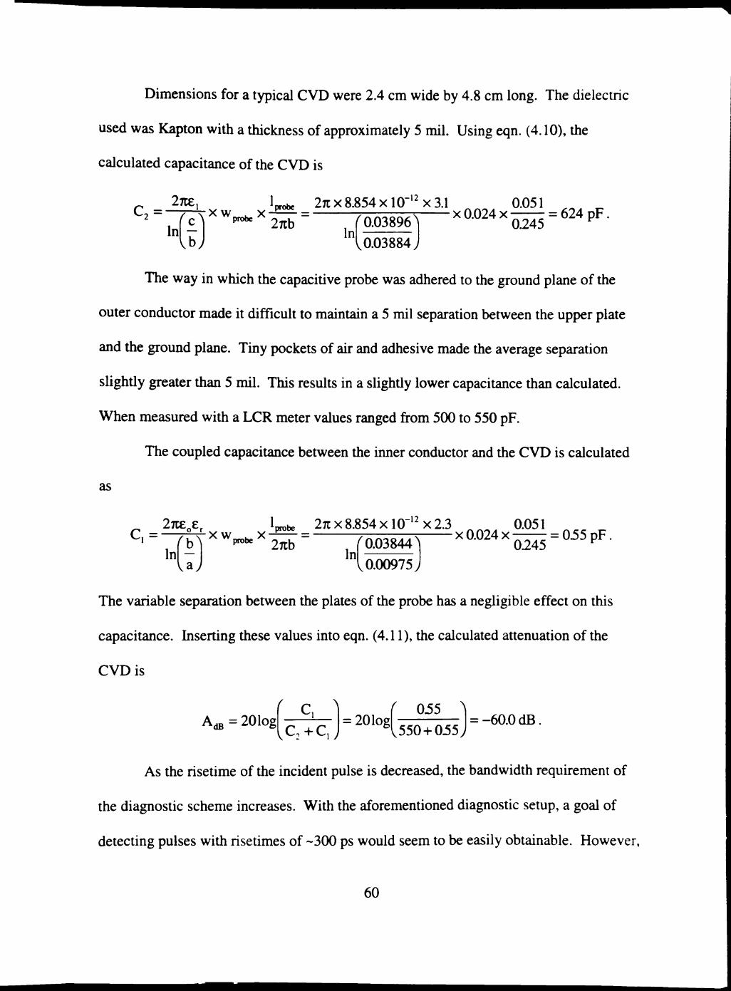
Dimensions for a typical CVD were 2.4 cm wide by 4.8 cm long. The dielectric
used was Kapton with a thickness of approximately 5 mil. Using eqn. (4.10), the
calculated capacitance of the CVD is
r ^ 1 ^ 2 ~
1. -12
In ^ c A ^ ^
Vh) P ^ 27Cb
27C X 8.854 X10"'X 3.1
In r 0.03896
X 0.024 X
V 0.03884 j
0.051
0.245 = 624 pF
The way in which the capacitive probe was adhered to the ground plane of the
outer conductor made it difficult to maintain a 5 mil separation between the upper plate
and the ground plane. Tiny pockets of air and adhesive made the average separation
slightiy greater than 5 mil. This results in a slightiy lower capacitance than calculated.
When measured with a LCR meter values ranged from 5(X) to 550 pF.
The coupled capacitance between the inner conductor and the CVD is calculated
as
C. = 27C£o£r Iprobe — T T T X W ^ . X ——
^b^ p™** 27:b In
27C X 8.854 X10"' X 2.3 0.051 X 0.024 x-r^TT = 0^5 pF
va In
0.03844 \
1,0.00975; 0245
The variable separation between the plates of the probe has a negligible effect on this
capacitance. Inserting these values into eqn. (4.11), the calculated attenuation of the
CVD is
AdB = 201og ' C, ^
V V_2 ' ^ 1 J
= 201og f 055 ^
,550-1-Oi5> = -60.0 dB.
As the risetime of the incident pulse is decreased, the bandwidth requirement of
the diagnostic scheme increases. With the aforementioned diagnostic setup, a goal of
detecting pulses with risetimes of -300 ps would seem to be easily obtainable. However,
60
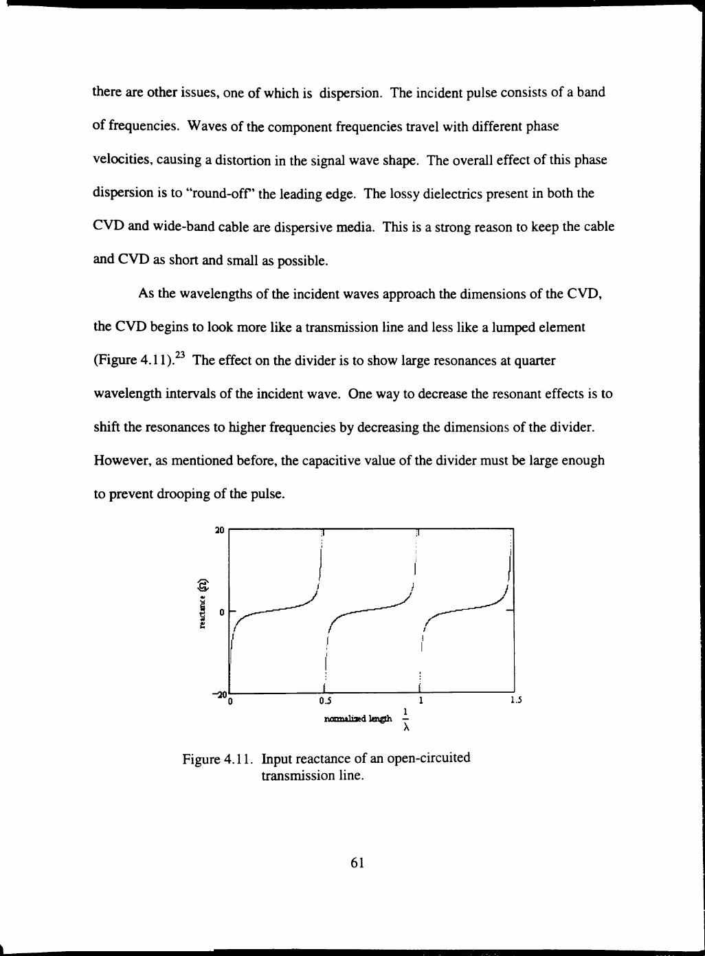
there are other issues, one of which is dispersion. The incident pulse consists of a band
of frequencies. Waves of the component frequencies travel with different phase
velocities, causing a distortion in the signal wave shape. The overall effect of this phase
dispersion is to "round-off the leading edge. The lossy dielectrics present in both the
CVD and wide-band cable are dispersive media. This is a strong reason to keep the cable
and CVD as short and small as possible.
As the wavelengths of the incident waves approach the dimensions of the CVD,
the CVD begins to look more like a transmission line and less like a lumped element
(Figure 4.11). The effect on the divider is to show large resonances at quarter
wavelength intervals of the incident wave. One way to decrease the resonant effects is to
shift the resonances to higher frequencies by decreasing the dimensions of the divider.
However, as mentioned before, the capacitive value of the divider must be large enough
to prevent drooping of the pulse.
©
-20
nacm«lla»d length — A
Figure 4.11. Input reactance of an open-circuited transmission line.
61

^
Probe Calibration
If the diagnostic semp is assumed to be a causal, linear-time-invariant system
(LTI), the output y(t) can be found from
t
y(t) = Jx(x)h(t-T)dx, (4.13) 0
where x(t) is the input and h(t) is the impulse response of the system. A schematic of an
LTI sytem in the time domain is shown in Figure 4.12.
y(t) ^
Figure 4.12. Diagram of an LTI system in the time domain.
The impulse response of the system can be found by inputting a delta function. For
example,
t t
y(t) = Jx(T)h(t - T)dT = J6(T)h(t - T)dT = h(t). (414) 0 0
If an impulse could be applied to the system, a pulse of width on the order of tens
of ps, one could obtain an approximation of the impulse response of the diagnostic setup.
One could then obtain an approximation of the acmal input pulse by knowing the output
and impulse response. The practical limitation of this method is in obtaining and
applying a known pulse with a width of several ten's of ps and of a voltage high enough
to provide a CVD signal with an adequate signal to noise ratio.
62
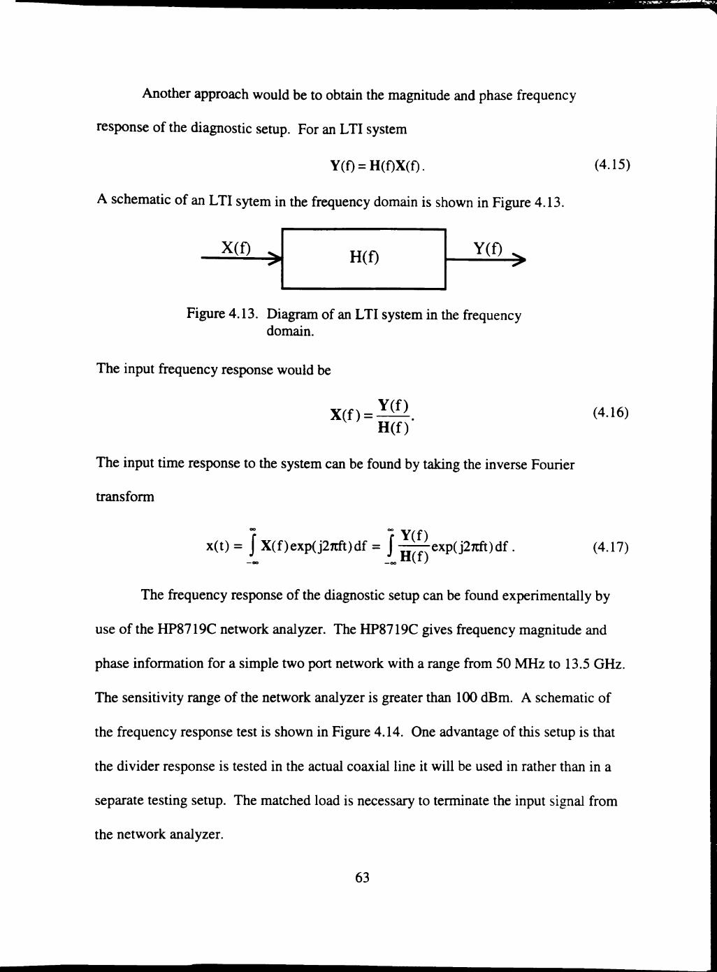
Another approach would be to obtain the magnimde and phase frequency
response of the diagnostic semp. For an LTI system
Y(f) = H(f)X(f). (4.15)
A schematic of an LTI sytem in the frequency domain is shown in Figure 4.13.
Y(f) ^
Figure 4.13. Diagram of an LTI system in the frequency domain.
The input frequency response would be
X(f) = X(Il. (4.16) H(f)
The input time response to the system can be found by taking the inverse Fourier
transform
x(t) = J X(f)exp(j27rft)df = J ^j^exp(j27cft)df. (4.17)
The frequency response of the diagnostic semp can be found experimentally by
use of the HP8719C network analyzer. The HP8719C gives frequency magnitude and
phase information for a simple two port network with a range from 50 MHz to 13.5 GHz.
The sensitivity range of the network analyzer is greater than 100 dBm. A schematic of
the frequency response test is shown in Figure 4.14. One advantage of this setup is that
the divider response is tested in the acmal coaxial line it will be used in rather than in a
separate testing setup. The matched load is necessary to terminate the input signal from
the network analyzer.
63
Wide-Band Matched Load
Figure 4.14. Calibration semp of frequency and phase response test.
The resulting frequency magnimde and phase response are shown in Figures 4.15
and 4.16, respectively. The magnimde response is relatively flat from dc to 1.5 GHz at
an attenuation of-60 dB. At 1.5 GHz the response falls about 4 dB.
1 2 Frequency (GHz)
Figure 4.15. Frequency magnimde response of a CVD.
270
180 c/l U H 90 u "O
r 0 t/> CQ
x: a. -90
-180
-270
1 1
— » .
—
V X - \ - ^
1
\ \ \
\ \ \ 1
\ \ \
k k \ I \ \ \ \ \ \ \
\ 1 >
1
1
\
0 1 2
Freq uency (GHz)
1
\ X Nv
>v \
^
1 3
Figure 4.16. Phase response of a CVD.
64
f0m^»d t.m^ <r**l*J&[^

In Figure 4.17 is displayed the frequency spectmm of a 4(X) ps risetime pulse
detected by a CVD. Also shown in Figure 4.17 is the frequency spectrum of the same
pulse after software compensation. This software compensation is an algorithm of eqn.
(4.17) using the frequency and phase response of the CVD obtained from the HP8719C.
Note the negligible change in frequency spectra between the compensated and
uncompensated waveforms.
0.8
I, H
O
a
0.6
0.4
0.2 -/ \
vine omp ens ate d
compensated
V V/VsA X
0.23 0.5
frequency (GHz)
0.75
Figure 4.17. Normalized frequency spectmm of compensated and uncompensated waveforms.
The normalized gap voltage waveforms, both compensated and uncompensated,
are shown in Figure 4.18. Note that the waveforms are nearly identical. It can safely be
said that the response of the CVD is capable of following pulse waveforms with risetimes
on the order of 4(X) ps.
65

fc> .-'r-.-jj?T^£^^«u-..r8s:-3J
OJ
0 -
-02-
DO
H
"5 -0.6 o G
-0.8
-1
-1.2
\ -N .
xtficontpensated
— cosqiensated
V - i,' ,J-:'
4 6
time (nsec)
. /
: • /
10
Figure 4.18. Normalized voltage of compensated and uncompensated waveforms.
Another calibration method was performed on the CVD. A 1 kV. 8(X) ps risetime
pulse from a reed switch pulser is applied to the coaxial line. The semp is shown in
Figure 4.19. An advantage of this semp is that the input pulse can be recorded at the
wide-band attenuator at the same time the output of the CVD is recorded.
To Oscilloscope
Switcfa To Oscilloscop)e
Wide-Band Matched Load
Figure 4.19. Calibration semp with known input pulse.
66
rffitV-:^^ • ^ - ^ • " — — "
The result of this calibration method is shown in Figure 4.20. Notice that the
output signal from the CVD follows the input pulse fairly accurately at the front of the
pulse. After 1 ns the output from the CVD begins to droop as compared to the input
pulse.
2 3
Time (ns)
Figure 4.20. Normalized voltage of the applied pulse and CVD pulse.
67
CHAPTER V
EXPERIMENTAL RESULTS
Introduction
This chapter presents the experimental results of the investigation into the
breakdown characteristics in the nanosecond and subnanosecond time regime for several
gases and liquids. These characteristics include electric field strength versus breakdown
time, dielectric strength dependence on polarity, statistical time lag, and streak camera
images of arc formation. The results are compared with data collected by others and
existing theoretical predictions. Finally, an empirical fit for these data is presented.
E-field versus Breakdown Time for Gas
Initial investigations into E-field versus breakdown time in gases focused on
breakdown times from 1 to 4 ns and pressures up to 11 MPa (16(X) psi). The voltage
source used in this experiment was the SEF-303A pulser without a peaking gap. This
provided gap voltages up to 350 kV. Figure 5.1 shows typical voltage waveforms at the
cathode and anode for high pressure gas with a time to breakdown of approximately 3 ns.
68
-400f
- 3 0 0 ->
tax) eo S -200-o >
1 -100-
100 0
Cathode
1 1 4 6
time (nanoseconds)
8 10
Figure 5.1. Voltage waveforms at the cathode and anode for H2 at 9 MPa (1300 psi) and 1.8 mm gap spacing.
Figure 5.2 presents peak E-field versus time to breakdown measurements for
various gases. Gas pressures were chosen as high as possible, limited only by bottie
pressure. The E-field across the gap is essentially uniform between the hemispherical
electrodes at the chosen gap distances of 1 to 5 mm. This assumption is verified by the
field distribution calculated by the Maxwell 3D simulation program presented in Chapter
2. Therefore, the E-field is simply the voltage difference across the gap divided by the
gap distance.
69
5
4.5
f " 1 3 - 2.5
1 2
0.5
0 J
• ^ w AvV-^ \ V ^ ^
V*t!l~*' • • ^^^
* ~ ^ ^—%^
) 2 4 (
time (ns)
— • — A i m MPa (1600 psi)
—•—Hydrogen 9.7 MPa (1400 psi)
—A—Nitrogen 11 MPa (1600 psi)
X SF6 2.4 MPa (350 psi)
— 5 i ^ Helium 6.9 MPa 5 (1000 psi)
Figure 5.2. Peak E-field versus time to breakdown for various gases.
A common way in which this type of breakdown data is presented is scaled with
pressure. The data in Figure 5.2 are presented in such a manner in Figure 5.3. Pressure is
in units of pascal. Also, a log-log graph is used.
1 .OE+04
(0
S 1.0E+03 E u
2 1.0E+02
UJ
1.0E+01
1.0E-06
^^""NifX
1 .OE-05
PMime (kPa)^(sec)
1 .OE-04
Air
Hydrogen
• Nitrogen
•SF6
"Helium
Figure 5.3. E-field versus breakdown time scaled with gas pressure for various gases.
70
The investigation of E-field versus breakdown time for gases was extended down
to breakdown times of 6(X) ps and up to gap voltages of 350 kV. This was accomplished
with a modification of the SEF-303 A pulser in which a oil-filled peaking gap was added.
Figure 5.4 shows E-field versus breakdown time for various gases at these shorter
breakdown times.
3
? 2 u
t 1.5 2 •
0.5
0
(
. ... 1
i iJ^..+
^
) 0.5
^ X
• j
1
time (ns)
• 1.3 mm gap at 2.75 MPa (400 psi)
X1.3 mm gap at 4.15 MPa (600 psi)
+1.3 mm gap at 5.2 MPa (750 psi)
1.5 2
Figure 5.4. E-field versus breakdown time for air with breakdown times down to 600 ps.
These data can also be presented in a Paschen curve. In Figure 5.5 is breakdown
voltage versus pressure times gap distance for various gases. Also shown is the Paschen
curves for these gases for dc breakdown. From these curves the overvoltage percentage
in eqn. (2.24) can be calculated.
71

asgv vs-. .
1.0E+03
CO 0>
1.0E+02
1.0E+01
I 1
. • ^ i
u .4
#
; * ; ; ; A—'—•—'—r-
# , ! . ^-^^
. 1 1 1
1 i 1 1 1 !
. •v'
\ ^ '
: 1 ' ! j : 1
1.0E+02 1.0E+03
pd (atrnXmils)
\ air I hydrogen
V SF6
— airdc
— hydrogen dc
— .SF6dc
1.0E+04
Figure 5.5. Paschen curve for various gases.
The ability to compare these data with data collected by others is limited.
Breakdown data for gases at these pressures and fast times are nonexistent. Therefore,
comparison can only be made on a relative basis. The only known empirical curve at
these time lengths is that of Felsenthal and Proud.^ Their curve for air and the data
collected by the author are displayed in Figure 5.6.
Notice the disparity between the two sets of data. The F and P values for E/P are
lower than observed by the author. In acmality, the comparison between these two sets
of data is not equal. The time to breakdown of this set of the F and P data are longer (>10
ns).
72
'*.'.• •a.vA
J 4 ** . •%, .
jxrasTjJ:
1 .OE+03
o
I 1.0E+02
a UJ
1.0E+01
1.00E-06
^~F&P empirical curve for air
• Air at 21 kTorr
A Air at 31 kTorr
X Air at 38 kTorr
1 psi = 52 Torr
1.00E-05
p*t (TorrKsec)
1 .OOE-04
Figure 5.6. Comparison between F&P empirical and author's data of breakdown in air.
A comparison of the collected gas breakdown data can be made with the
empirical relationship, eqn. (2.23), developed by T.H. Martin. This empirical formula is
pt = 97800 .P .
where p is gas density in g/cc, E is average electric field kV/cm, and t is time to
breakdown in seconds. Martin's curve fits a variety gases including air, N2, He, and
others. A comparison of observed breakdown data and the Martin curve is shown in
Figure 5.7.
73
r-> "w CO Q .
Q- o in o 1 - - *
(Q CO Q. Q-
^ 2 o te * - C\j CO « -1 - CO
CO C L
CO ' ^
D> £ E E E CO
CVJ • . -
• •
c
^-p-
, ^_ ^_ -^^—.—_ - —
- •
J • r
! • -
1 , , ! !
1
D + UJ o .,_
Q. O O
Q.
i n 1 ^ CM
(0 Q. (0 O )
E E CM
n
-
a T
-'
'<n Q . o o
CO Q.
i n • ^
TT
(0 Q . CO O )
E E
• ^
•
—'—
—— - -
. -
>
- -
'</) Q .
O O CO
CO Q. ^ in
T t
CO Q . CO
E E
CO
• ^
+
—t
' 1
-^
-
X
4* - —
a o in c . t:^ CO
^ ^ Q. IE 2 CM CM in
'^ 13 CO Q .
CO ^ ^
D) E E E E CO
• ^ • ^
• 1
1_^ —'— '
'
. . . -
• - - -K X . .
* ^
J I —
^ ^ : i
CO
+ UJ o o o
, . Ui
o. o o CO
CO
a. 2 • » —
CM ^ CO
CM
I Q CO
F E
CO CM
•
CO Q .
O
o in (0
Q.
in
CO
« CO
CM I Q . to Oi
E E CM
•
(0 (0
o o o in in CM
CO m Q. Q.
in CO "* i^ CO - i -
co c5 CM CD I I Q. to C3)
F E
Q. CO
F E
CD CO
CM ••
< X —
I '
—
o 3 O c "t: CO
1 1 §
i
-M—
1
—* *
--: I
'
— --
-—-
:
•
• / 1 f J
(
L c c
CO
a in CO
CO
a. j ^
o in CM
CO
(0
C3)
E E CM
O
+ u D 3
--
O
+ UJ q —
CO 1
UI o o o ^
CO 1
UJ o o
CO
U J
q
CO
ui o d> o
'ST c u B>
> r3 •—
—< c c . -
u, — - ^ J= y. . - ^
OX) ^
-a "^
cj cd U CL
u S
r--l o u Urn 3 ex) uu
(oo/6)/(uio/A>l) d/p|OU-3
74
i • o ^
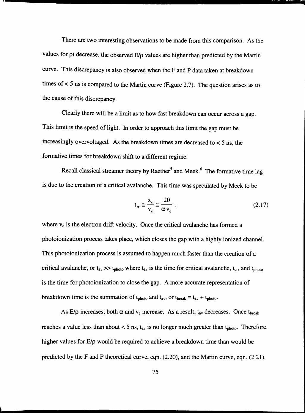
There are two interesting observations to be made from this comparison. As the
values for pt decrease, the observed E/p values are higher than predicted by the Martin
curve. This discrepancy is also observed when the F and P data taken at breakdown
times of < 5 ns is compared to the Martin curve (Figure 2.7). The question arises as to
the cause of this discrepancy.
Clearly there will be a limit as to how fast breakdown can occur across a gap.
This limit is the speed of light. In order to approach this limit the gap must be
increasingly overvoltaged. As the breakdown times are decreased to < 5 ns, the
formative times for breakdown shift to a different regime.
Recall classical streamer theory by Raether and Meek. The formative time lag
is due to the creation of a critical avalanche. This time was speculated by Meek to be
X, 20 tcr= — = - — ^ (2.17) Ve CXV
where Ve is the electron drift velocity. Once the critical avalanche has formed a
photoionization process takes place, which closes the gap with a highly ionized channel.
This photoionization process is assumed to happen much faster than the creation of a
critical avalanche, or tav»tphoto where tav is the time for critical avalanche, tcr, and tphoto
is the time for photoionization to close the gap. A more accurate representation of
breakdown time is the sunmiation of tphoto and tav, or tbreak = tav + tphoto-
As E/p increases, both a and Ve increase. As a result, tav decreases. Once tbreak
reaches a value less than about < 5 ns, tav is no longer much greater than tphoto- Therefore,
higher values for E/p would be required to achieve a breakdown time than would be
predicted by the F and P theoretical curve, eqn. (2.20), and the Martin curve, eqn. (2.21).
75

The second discrepancy between the data collected and the Martin curve is the
large difference between the E/p values for H2. The Martin curve was developed for
various gases, however, H2 was not one of these gases. It is possible that the ionization
coefficient, a, for H2 is much less than a for the other gases observed for a given E/p.
This would require higher E/p values for H2 to obtain equivalent breakdown times for
other gases.
An Empirical Relationship for Gas Breakdown
An empirical relationship for the relationship between E-field and breakdown
time for gases is attempted. Figure 5.8 displays breakdown data for air, relating E/p
versus pt on a log-log scale. Also shown is the Martin curve of eqn. 2.23 and selected F
and P data of breakdown of air at low pressures and fast breakdown time (~ Ins).
The expression for the curve fit shown in Figure 5.8 is
E_
P
f
0.9 j
2.25
(5.1)
where E is in kV/cm, p is gas density in g/cc, and t is in nanoseconds. This expression
fits the breakdown data for times less than 5 ns and gases tested which include air, N2,
SF6, and He. The breakdown data collected on H2 does not fit well with eqn. (5.1).
An additional expression has been fitted to the H2 breakdown data. This
expression is
E_
P ^0.9;
2.05 (5.2)
Notice that the only change is in the value of the exponent. 76

^
o
It 1 1 1 ^ S 1 1 ^ ==- =H ^ a a
Cvj
cB IB
p h» CM 13 ^
in
• *
13 ^
• ^
'^ ia ^ cti
CJ id
n k .
CVJ in ffi ^ cd CO Q - TO to Q . ffl
S I §; S I I
8 I I ^ £ ig I £ S 1 S 8 I 5 I « R iri i l i S CV] 5{j! CO ••-
• 1 3 rt 13 13 JNl 13 JM OJ
CM fc CO
CM 1 - : CO CO
X H
cB
k
13 13
CO fc t o CO c\i CO csi -r-:
• ^ X X
- H i
1 i 1
[ l l l l r
j I
' '<
\ I I I ! 1 = — ^ ^
,
. ^^ ,
- — ' 1-- — r ^
* - - ' ' '
1 1 1 1 1
H ^ \ : 1
M M M M
M l
. , . ; -*
r~—'—'—', H ~ ^
- -^^-^^m^ X '
= ^ ^ - ^ . : : : : - — ^ ^ ' . — • — ' — ' — ' — • — ' — = ^
' '
^ J £-J^ 9 f^+^
# - - — - -f
! y ' / ' I
I I I ! 1 1 1 1 j — \ 1 ! '—< 1
i 1 ! ' ' 1
1 I
M
#
i
f
,r i '
#
s #
#
* 1 - 1 ! / !===
\ 1—1 § M — h 1—• / h t + ^ \—^--/ "+^^
' / ' ' ' ' i
M \— _ — - M - ^ 1—
J 1
1—"~~^ ^—# —
• J
ff
K 1
—§—i— TH—^— r—'—'—1
— ^ - — •
-~- ^—,
— 1 — ' — 1 —
I
^ a
c '•3
D ^
.2 ^ > -S o o 2 < 03
c > "S ^ 3 T3
3 .S i ^ t: ^
0 0
in
3
tu
(33/B)/(uJ3/A>l) " / P i e u - i
77
i
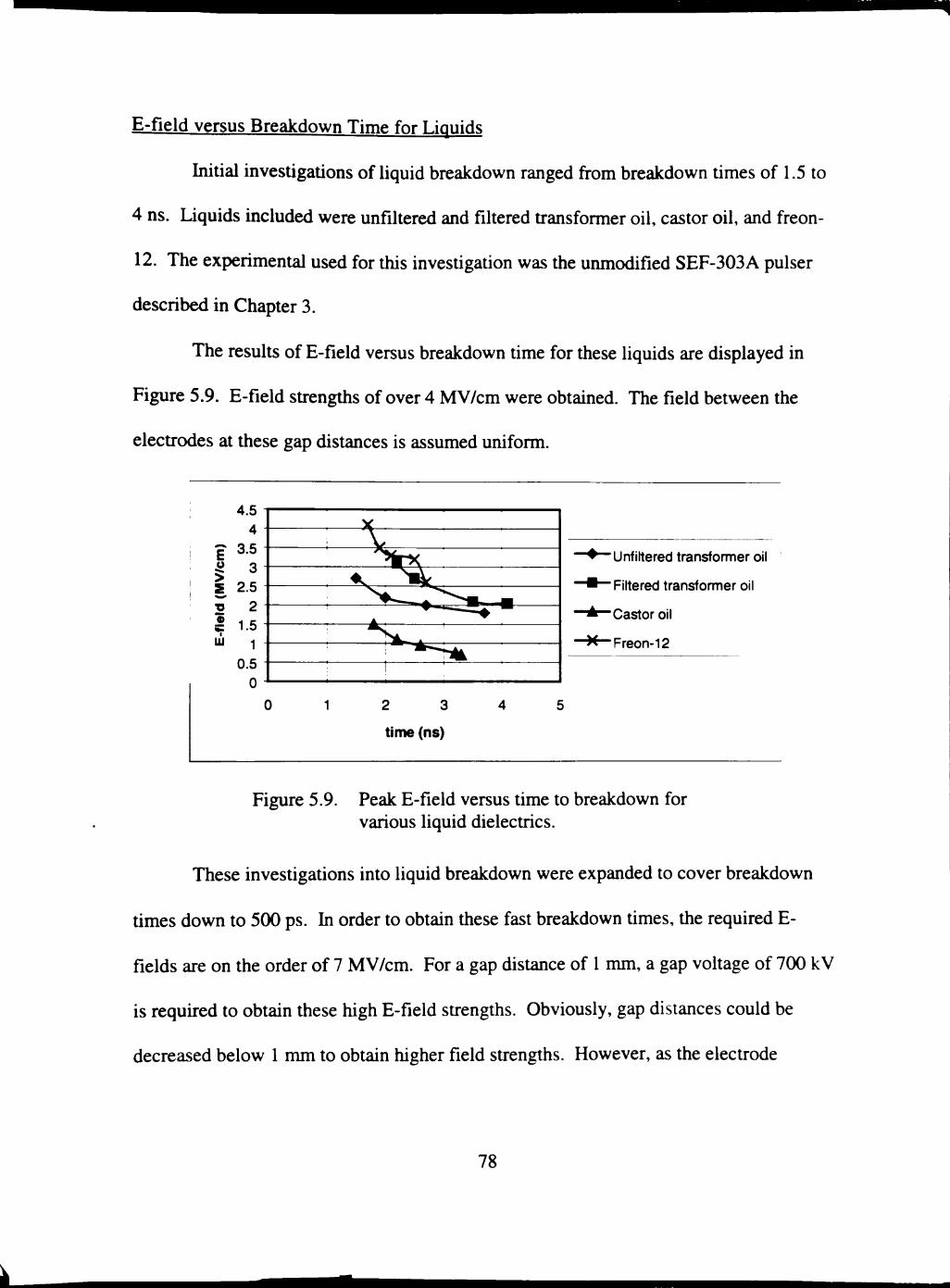
E-field versus Breakdown Time for Liquids
Initial investigations of liquid breakdown ranged from breakdown times of 1.5 to
4 ns. Liquids included were unfiltered and filtered transformer oil, castor oil, and freon-
12. The experimental used for this investigation was the unmodified SEF-303 A pulser
described in Chapter 3.
The results of E-field versus breakdown time for these liquids are displayed in
Figure 5.9. E-field strengths of over 4 MV/cm were obtained. The field between the
electrodes at these gap distances is assumed uniform.
time (ns)
"Unfiltered transformer oil
"Filtered transformer oil
"Castor oil
"Freon-12
Figure 5.9. Peak E-field versus time to breakdown for various liquid dielectrics.
These investigations into liquid breakdown were expanded to cover breakdown
times down to 500 ps. In order to obtain these fast breakdown times, the required E-
fields are on the order of 7 MV/cm. For a gap distance of 1 mm, a gap voltage of 700 kV
is required to obtain these high E-field strengths. Obviously, gap distances could be
decreased below 1 nmi to obtain higher field strengths. However, as the electrode
78
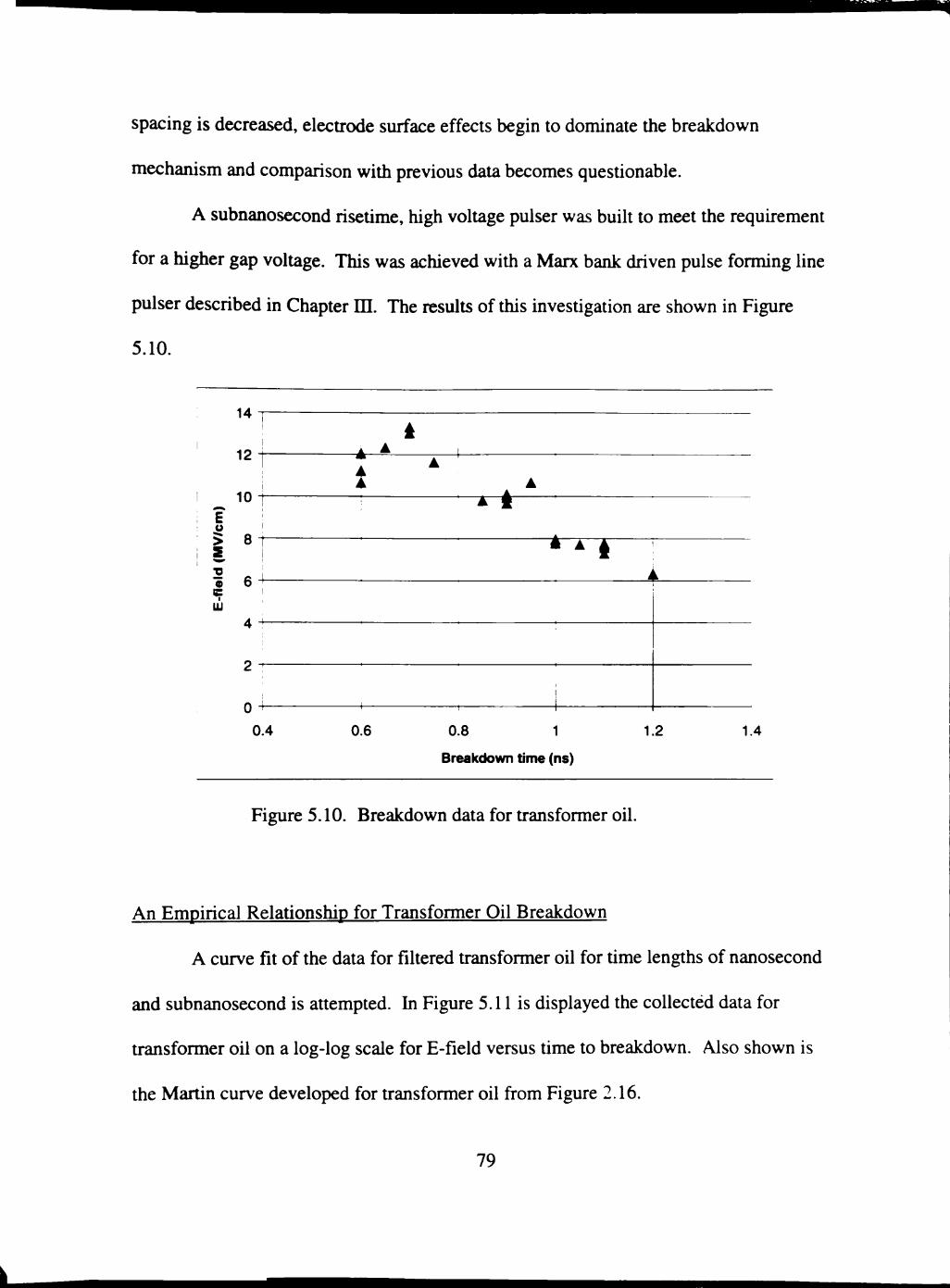
spacing is decreased, electrode surface effects begin to dominate the breakdown
mechanism and comparison with previous data becomes questionable.
A subnanosecond risetime, high voltage pulser was built to meet the requirement
for a higher gap voltage. This was achieved with a Marx bank driven pulse forming line
pulser described in Chapter IE. The results of this investigation are shown in Figure
5.10.
'
1 ^^ E o >
; s "D O C
14
12
10
8
6
UJ
4 ^
0 4 -
0.4
t
0.6
rt
* ^ ^
0.8 1
Breakdown time (ns)
1.2 1.4
Figure 5.10. Breakdown data for transformer oil.
An Empirical Relationship for Transformer Oil Breakdown
A curve fit of the data for filtered transformer oil for time lengths of nanosecond
and subnanosecond is attempted. In Figure 5.11 is displayed the collected data for
transformer oil on a log-log scale for E-field versus time to breakdown. Also shown is
the Martin curve developed for transformer oil from Figure 2.16.
79
100
E o >
S 10
UJ
1 100.0E-3
• 0.8mm gap • 0.6mm gap A 0.4mm gap • nanosecond data - Martin curve - - Curve Fit - - JC Martin Curve
1.0E+0
time (nsec)
10.0E+0
Figure 5.11. Empirical curve fit for collected transformer oil breakdown data.
The expression relating E-field versus time to breakdown is
E = 7.9t -0.95 (5.3)
where E is in MV/cm and t is in nanoseconds. This expression is only valid for times less
than ~5 ns. At greater times, the Martin curve becomes valid. The J.C. Martin curve,
shown in Figure 5.11, for breakdown voltage in transformer oil is
E2 = 80
'eff
(5.4)
where E is in MV/cm and tgff is in nanoseconds. The effective time, teff, is the duration of
the pulse between 63% and 100% of the peak voltge reached and ranged from 150 to 300
ns. This approach was one of measuring the threshold voltage before breakdown rather
than breakdown time. The threshold voltage approach and the long duration times of the
J.C. Martin curve result in the discrepancy of curves seen in Figure 5.11.
80
i.-ri^ii iifiiiii^^iisssaBk
Dielectric Breakdown Strength Dependence on Polaritv
The polarity dependence of dielectric breakdown was discussed in Chapter n.
Polarity dependence is typically caused by the presence of space charge about the point in
a point-plane electrode geometry. A point-cathode will typically have a higher
breakdown strength than a point-anode for a given gap spacing, voltage, and gas pressure.
The presence of this effect is investigated for nanosecond breakdown times.
The dielectrics investigated were transformer oil and air. The point-plane
breakdown data for transformer oil are shown in Figure 5.12. The negative-point
arrangement has a higher E-field breakdown strength, especially at the shorter breakdown
times. The breakdown strength of the negative-point arrangement is approximately 50%
greater than the positive-point. This value is in agreement with findings reported by J.C.
Martin 12
m lU
9 -
? 8-o ^ 7 -S ^ 6 -^ 5 -1
UJ
0, 4 -
i 2-1 -
U i
(
^
A A A A Jt'
o neg. point .33 mm gap
D neg. point .49 mm gap
• pes. point .49 mm gap
A pes. point .65 mm gap
\— 1 '
D 1 2 3
time to breakdown
Figure 5.12. Breakdown data for point-plane geometry in transformer oil.
81

Breakdown data of a point-plane geometry in air at different pressures are shown
in Figure 5.13. Again, the negative point has a higher breakdown strength. The
fractional increase in breakdown strength for the negative point seems to decrease with
an increase in gas pressure. This amount varies from approximately 20 to 90%. Values
reported by J.C. Martin'^ are as high as 100%.
1.6-.
1.4-
? 1-2-
1 '• » 0.8-1
UJ
S. 0-6-a 1 0.4-<
0.2-
0-(
O
o DO D
D
• • •
3 0.5 1 1.5 2 2.5
Breakdown time (nsec)
• BDS. point 200 PSI
n Neg. point 200 PSI
• BDS. point 400 PSI
O Neg. point 400 PSI
Figure 5.13. Breakdown data of a point-plane geometry in air.
Streak Camera Images
Images of the arc formation during nanosecond and subnanosecond breakdown
were recorded with a fast streak camera. The semp of this procedure was described in
Chapter m. Dielectric media investigated were transformer oil and air. Of specific
interest is the propagation velocity of the streamer and the time it takes for the channel to
become highly ionized.
82
1^ -^J^tmwMW»^^-:A¥'^-^r- • w i i . ] j ; i j •»» jagliittiife:^
Streak images of a 1 mm wide transformer oil-filled gap were taken. The applied
voltage pulse had a 400 ps risetime, a 4.5 ns width, and a magnitude of 300 kV. In
Figure 5.14 is shown a 5 ns streak of the gap some time after the arc has been established.
u
S Z3
4 6 distance (mm)
Figure 5.14. 5 ns streak of 1 nam transformer oil filled gap after arc formation.
In Figure 5.15 a and b are streak images of the 1 mm transformer oil gap at the
beginning of arc formation at streak lengths of 5 and 10 ns, respectively. The transition
from the onset of ionization to gap closure appears to occur in approximately 500 ps. A
closer view of the beginning of the arc formation in the 5 ns sweep is shown in Figure
5.16.
83
•--^.^mjQiSSSfi^^fif^t^Uffii.irr''-'- - —.rn^sSM^USSSi.
-^mnnjMitfffiflmflTI"''' 'I'l vif'n rv 'iYiKAV>mi"-'"'"'"
u
•3, a
0 4 6 distance (mm)
(a)
4 6 distance (mm)
(b)
Figure 5.15. Streak images of the beginning of the arc formation of a 1mm transformer oil gap at time lengths of (a) 5 ns and (b) 10 ns.
84
1 WfiJf^^^^WiaAtaiiftufApff^^^ ^i*BrrfBM<i
' ^^' ' "• • - - r " — ^ ^ h ^ ^ ^ t . ^ t i Y - ^ r - " ^ " " ' "
o
distance (mm)
Figure 5.16. Close up view of arc formation in the 5 ns streak.
An estimate of gap-closure velocity for oil can be made from Fig. 5.16. For a 1
nmi gap and a 5(X) ps closure time, the gap-closure velocity for oil is
Voil = 0.1 cm
0.5 ns = 0.2 cm
ns (5.5)
Streak images of gas gaps have also been captured. Compressed air at a pressure
of 400 psi was investigated. The first streak image is of a 4 mm gap at a 10 ns sweep
(Figure 5.17).
85
^ ^ r*^t-ft:«9w^r-/-."-^t- •-- rr^ WiffjefUft///tiittmi9JtgBSV^,..y - • •rviij.<o>jBrrjCgjM
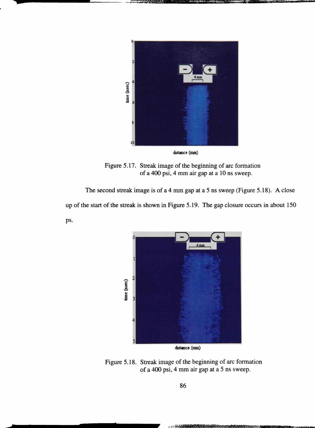
•IS\VV».'»M-J'. . K-tSs:£iV/ys<aBBi»"rt.-jo*>.;. •••-•* i r ^ ^ g 2 ^ ^ ^ ^ ^ ^ ( ^ m j ^ M l
distance (nun)
Figure 5.17. Streak image of the beginning of arc formation of a 400 psi, 4 mm air gap at a 10 ns sweep.
The second streak image is of a 4 nam gap at a 5 ns sweep (Figure 5.18). A close
up of the start of the streak is shown in Figure 5.19. The gap closure occurs in about 150
ps.
o *i M
I
distance (mm)
Figure 5.18. Streak image of the beginning of arc formation of a 400 psi, 4 mm air gap at a 5 ns sweep.
86
•^•.fX/A Wimti^*Mffi^immjij^^,^sm - r i i ' i f i f i fg r
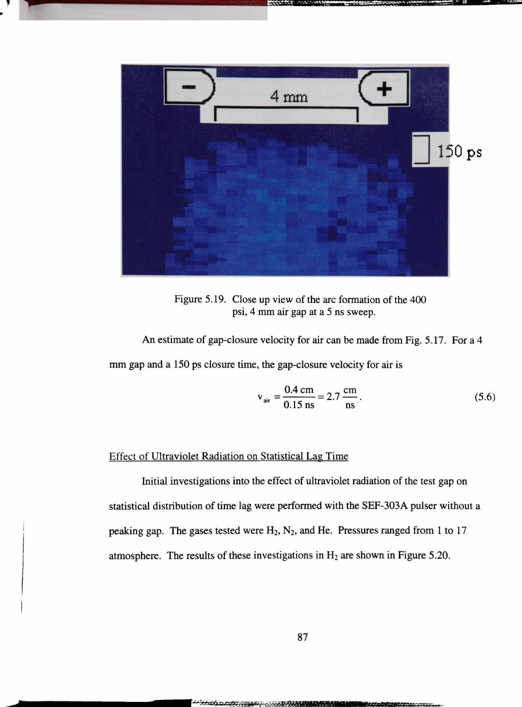
Figure 5.19. Close up view of the arc formation of the 400 psi, 4 mm air gap at a 5 ns sweep.
An estimate of gap-closure velocity for air can be made from Fig. 5.17. For a 4
nmi gap and a 150 ps closure time, the gap-closure velocity for air is
0.4 cm ^ ^ cm v„:. = = 2.7 — 0.15 ns ns
(5.6)
Effect of Ultraviolet Radiation on Statistical Lag Time
Initial investigations into the effect of ultraviolet radiation of the test gap on
statistical distribution of time lag were performed with the SEF-303 A pulser without a
peaking gap. The gases tested were H2, N2, and He. Pressures ranged from 1 to 17
atmosphere. The results of these investigations in H2 are shown in Figure 5.20.
87

• CXTOWt*.';-."K-ssL«wao?4j»\ s^^-
I f l 1 o
16
14
12 -
i 10
? 8 ^ 6
4
2
0
— -
1
--
-
. _ _ _ ._
—
r rTFtH 1 r • 11
1.4
1.45
1.5
1.55
1.6
1.65
1.7
1.75
1.8
Breakdown time (nsec)
nUVon
• UVoff
(a)
8 -[
7 -
6
o o c * A
3 4
S3 2 1 -
u -*
1 —
4
—
il hriii 11
1.75
1.8
1.85
1.9
1.95
2.05
2.1
2.15
2.2
Breakdown time (nsec)
nUVon
• UVoff
(b)
Figure 5.20. Distribution of breakdown times in H2 for (a) 1 atm with a 4.5 mm gap, 50 kV gap voltage and (b) 17 atm with a 4 mm gap, 200 kV gap voltage.
88

Referring to Figure 5.20a, when the gap is radiated with UV the statistical lag
time is decreased dramatically. This is due to the large number of free electrons present
in the gap prior to the arrival of the incident gap voltage. However, when the gas
pressure was increased (Figure 5.20b), the decrease in statistical lag time of a UV
radiated gap does not occur. This effect was observed in all three gases.
The first possibility is that the radiated UV does not reach the gap due to
photoabsoption or scattering by the high pressure gas. Therefore, the plethora of free
electrons in the gap are not present as they are for the gaps at atmospheric gas pressures.
After some simple calculations this is probably not the case.
Photoabsorption of ultraviolet radiation is caused by ionization of the medium.
Recall Figure 3.13 which shows the transmittance of the fused sihca window. Notice that
smallest wavelength which can pass through this window is 160 nm. Assuming a
uniform UV source across the UV spectrum from the Xenon lamp, the highest radiation
energies which will be in the gap is 7.75 eV. The ionization potentials for H2, He, and N2
are 15.4, 24.6, and 15.6 respectively. Therefore, the ultraviolet radiation energy is not
high enough to ionize the gases examined, however, with a work function of 4.5 eV for
brass, the UV radiation is high enough to free electrons from the brass electrodes.
Another approach is to calculate the attenuation of UV radiation through the
atmosphere and correlate it with the experimental setup. The transmittance of
monochromatic radiation along a path in air can be expressed as"
T = e-^^, (5.7)
where y is an attenuation coefficient and AL is the length of tiie path traversed by the
radiation. The attenuation coefficient y is given by
89
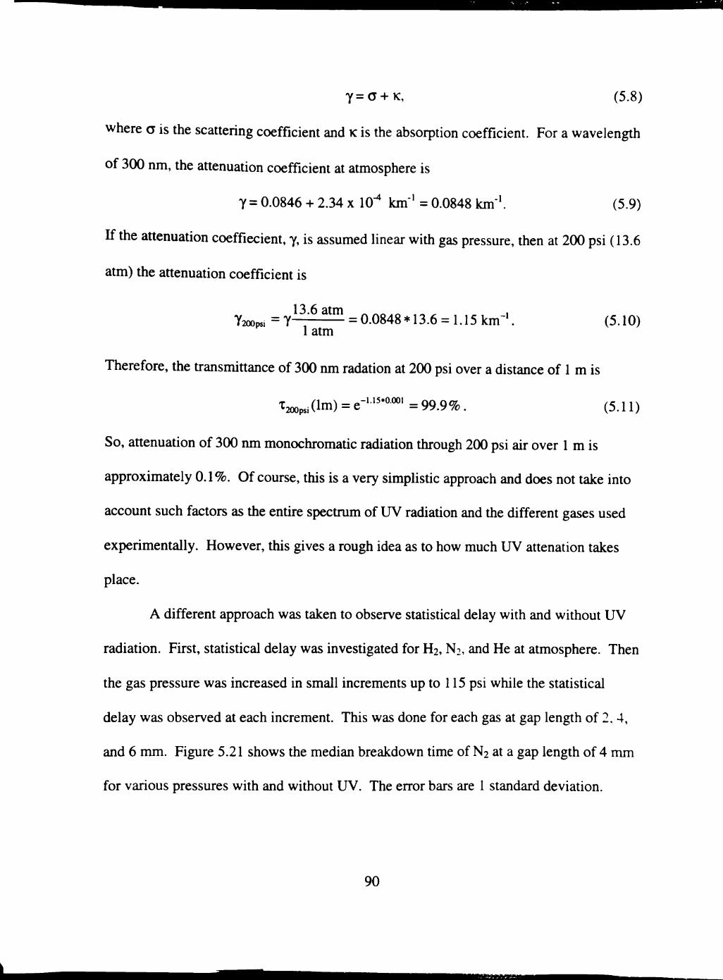
Y=a + K, (5.8)
where o is the scattering coefficient and K is the absorption coefficient. For a wavelength
of 300 nm, the attenuation coefficient at atmosphere is
Y= 0.0846 + 2.34 x 10" km' = 0.0848 km*'. (5.9)
If the attenuation coeffiecient, y, is assumed linear with gas pressure, then at 200 psi (13.6
atm) the attenuation coefficient is
Y200PS. = y i ^ : ^ ^ = 0.0848 * 13.6 = 1.15 km"' 1 atm
(5.10)
Therefore, the transmittance of 300 nm radation at 200 psi over a distance of 1 m is
'C2ooosi(lm) = e -1.15*0.001 = 99.9% (5.11)
So, attenuation of 300 nm monochromatic radiation through 200 psi air over 1 m is
approximately 0.1%. Of course, this is a very simplistic approach and does not take into
account such factors as the entire spectmm of UV radiation and the different gases used
experimentally. However, this gives a rough idea as to how much UV attenation takes
place.
A different approach was taken to observe statistical delay with and without UV
radiation. First, statistical delay was investigated for H2, N2, and He at atmosphere. Then
the gas pressure was increased in small increments up to 115 psi while the statistical
delay was observed at each increment. This was done for each gas at gap length of 2, 4,
and 6 mm. Figure 5.21 shows the median breakdown time of N2 at a gap length of 4 mm
for various pressures with and without UV. The error bars are 1 standard deviation.
90
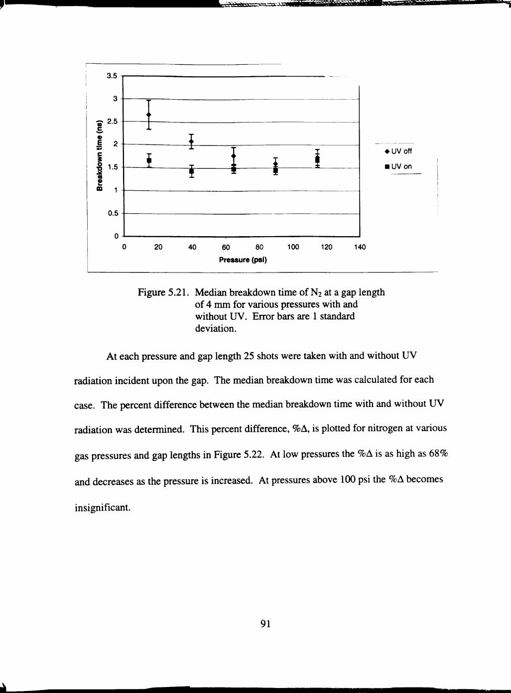
iKAA'i£!aXJss:?=ixxg:aa
3.5
^ 2 . 5
« £ 2 c € 1.5 CB
o 1 4
0.5
0 J
i i t
20 40 60 80
Pressure (psi)
100
• UVoff
• UVon
120 140
Figure 5.21. Median breakdown time of N2 at a gap length of 4 mm for various pressures with and without UV. Error bars are 1 standard deviation.
At each pressure and gap length 25 shots were taken with and without UV
radiation incident upon the gap. The median breakdown time was calculated for each
case. The percent difference between the median breakdown time with and without UV
radiation was determined. This percent difference, %A, is plotted for nitrogen at various
gas pressures and gap lengths in Figure 5.22. At low pressures the %A is as high as 68%
and decreases as the pressure is increased. At pressures above 100 psi the %A becomes
insignificant.
91
•' mmtmm •m-iCJii2Bia:.x»; ksiuraK
-2 m m gap ,
-4 m m gap
•6 m m gap i
140
Figure 5.22. Percent difference of median breakdown time between a nitrogen gap with and without UV radiation at various gap lengths versus gas pressures.
As the pressure is increased the gap voltage is increased in order to obtain
approximately the same breakdown time (-1.5 ns). The %A is plotted with respect to E-
field in Figure 5.23. As the E-field is increased, the %A decreases.
-2 mm gap
-4 mm gap
-6 mm gap
100 200 -10
300 400
E-f Mid (kV/em)
500 600 700
Figure 5.23. Percent difference of median breakdown time between a nitrogen gap with and without UV radiation at various gap lengths versus E-field.
92
k
The interesting case is when %A is plotted with respect to E-field/pressure as in
Figure 5.24. The %A is relatively independent of gap distance. When E/P is less than 5,
the %A becomes insignificant. However, when E/P is greater than 5, the %A increases
dramatically.
-2 mm gap •4 mm gap -6 mm gap
E/P (kV/cm)/(psi)
Figure 5.24. Percent difference of median breakdown time between a nitrogen gap with and without UV radiation at various gap lengths versus E-field/pressure.
A hypothetical explanation for these phenomena is presented. At high values of
E/P the free electrons, due to the UV radiation, present in the gap contribute significantiy
to the initial avalanche which leads to breakdown. The high E/P of the gap allows these
seed electrons to attain high enough energies to create the initial avalanche. As E/P is
decreased, these seed electrons contribute less and less to the initial avalanche until E/P
becomes so low that these seed electrons no longer contribute at all to the breakdown. In
this case, the supply of electrons which lead to the initial avalanche is from explosive
93
emission on the cathode surface. The applied E-field in excess of 100 kV/cm makes the
explosive emission process possible.
The %A versus E/P for H2 and He was also observed. These plots are similar to
those for N2. The plots are shown in Figures 5.25 and 5.26.
4 6 8
E/P (kV/cm)/(psi)
10 12
•2 mm gap •4 mm gap •6 mm gap
14
Figure 5.25. Percent difference of median breakdown time between a hydrogen gap with and without UV radiation at various gap lengths versus E-field/pressure.
94
v.'jitt'/iftfiftg

.!e<«crv?tr«
9 0 -
80-'
70 -
60 -
S 50 -
Q
5? 40 -
3 0 -
20 j
10 -
0^
•2 mm gap
•4 mm gap
•6 mm gap
10 12
E/P (kV/cm)/(psi)
Figure 5.26. Percent difference of median breakdown time between a helium gap with and without UV radiation at various gap lengths versus E-field/pressure.
95
•r/.'.v/Agrfeaifc:
S B
CHAPTER V
CONCLUSIONS
An attempt has been made to investigate the breakdown characteristics of gas and
liquid dielectrics at breakdown times ranging from 500 ps to 5 ns. Two different voltage
sources were used to produce tiie fast risetimes (400 ps) and high E-fields (>10MV/cm)
necessary to carry out these fast breakdown times. The experimental investigations were
comprised of breakdown times versus E-field strengths, breakdown strength dependence
on polarity, streamer formation analysis using a fast streak camera, and the effect of
incident UV radiation on the statistical distribution of breakdown time.
The goals set for the specifications of the voltage sources were achieved. A
simple modification of the SEF-303 A (inclusion of a peaking gap) allowed for a fast
risetime (4(X) ps) source with a variable voltage output that was easy to change. Another
source, a Marx bank driven PFL, was designed and built and met the specification
requirements of 400 ps ristime and 100 kV output. Modifications to the Marx bank and
peaking gap could allow for faster risetimes (<3(X) ps) and higher voltage outputs
(>1MV) in the fumre.
Experimental investigation into the E-field strengths achieved at various
breakdown times were successfiil. Although E-field strengths at these breakdown times
(>500 ps) have been attained by other investigators, nothing close to the high pressure
gas dielectrics used here has been examined. It was found that the E-field strengths
required to break down these high pressure gases at these short times (-500 ps) is higher
96
than predicted by others. These fast breakdown times require different empirical
formulas in order to predict breakdown strengths.
It was found that the breakdown strength of several gas dielectrics and
transformer oil is dependent on gap polarity. As predicted, in a point-plane electrode
geometry the negative point consistentiy attained higher breakdown strengths. The
amount of this difference is on the order, though somewhat less, than those observed b}
other investigators.
The results of the streak camera investigation of the streamer formation were
successful. Streamer formation of breakdown in transformer oil and air can be seen.
However, streamer formation in gas occurs faster than in transformer oil and the time
resolution is not as good. These results are most likely indicative of the breakdown times
observed (the breakdown time in air was faster than in transformer oil) than any other
factor. Streamer gap closure in tranformer oil and air occurred in approximate times of
500 and 150 ps, respectively (0.2 cm/ns and 2.7 cm/ns, respectively).
The investigation of the effect of UV radiation on the statistical namre of
breakdown time was successful. The effect of UV on statistical time lag on gases at
atmosphere pressure was dramatic, but at pressures of 1.4 MPa (200 psi) and above the
UV had no effect. A careful observation of statisitical time lag with and without UV. as
the gas pressure was incrementally increased, was made. It was found that UV effect on
statistical delay time is dependent on E-field/pressure and relatively independent on gap
length.
97
REFERENCES
1. D. Herskovitz, "Antennas and Transmission Systems: Wide, Wider, Widest," Journal of Electronic Defense, pp. 51-58, July, 1995.
2. F.J. Agee, D.W. Schofield, R.P. Copeland, T.H. Martin, J.J. Carroll, J. Mankowski. M. Kristiansen, and L. Hatfield, "A Review of Catastrophic Electromagnetic Breakdown for Short Pulse Widths," Proceedings ofSPIE '96, pp. 172-182, August, 1996.
3. D.G. Fink, Standard Handbook for Electrical Engineers, New York: McGraw Hill, tentii edition, 1968.
4. L.L. Alston, High Voltage Technology, London: Oxford University Press, 1968.
5. H. Raether, Electron Avalanches and Breakdown in Gases, Washington D.C: Butterworth, 1964.
6. J.M. Meek, Phys. Rev., 57, 722, 1940.
7. P. Felsenthal and J.M. Proud, Phys. Rev., 139, al796, 1965.
8. T.H. Martin, "An Empirical Formula for Gas Switch Breakdown Delay," Res. Sci. of Pulsed Power, Sandia National Labs, pp. 73-79, 1991.
9. J.C. Martin, Dielectric Strength Notes, 15, first printed as SSWA/JCM/679/71, AWE intemal publication, 1967.
10. E. Kuffel and W.S. Zaengl, High Voltage Engineering, Oxford, New York: Pergamon Press, 1984.
11. E.E. Kunhardt, "Nanosecond Pulse Breakdown of Gas Insulated Gaps," NATO AS! Series, Series B: Physics, Vol. 89a, New York: Plenum Press, 1983.
12. T.H. Martin, A.H. Guenther, and M. Kristiansen, J.C. Martin on Pulsed Power, Vol. 3, chap. 4, New York: Plenum Press, 1996.
13. A. Vorobyov, V. Ushakov, and V. Bagin, "Electrical Strength of Liquid Dielectrics at Voltage Pulses of a Nanosecond Duration," Electrotechnika, vol. 7, pp. 55-57, 1971.
14. SEF-303 A Compact High-Current Pulsed Power Source, Description and Technical Manual, Ehaterinburg, Russia, Electrophysical Instimte: 1991.
98
15. M. Mayerchak, Pulsed High Voltage Insulator Flashover in a Simulated Low Earth Orbit Environment, Master's Thesis, Texas Tech University, May, 1991.
16. V & L Products Inc, Optical Specifications, Berlin, NJ: 1997.
17. Hamamatsu Temporal Disperser, Description and Technical Manual, Middlesex, NJ: 1980.
18. J.H. Mason, "Breakdown of SoUd Dielectrics in Divergent Fields," Institute Monograph, No. 127M, April, 1955.
19. R. Hebner, 'The Measurement of High Current and Voltage Pulsed," AF Pulsed Power Lecture Series, No. 35, Texas Tech University, 1980.
20. W.A. Edson and G.N. Oetzel, "Capacitance Voltage Divider for High-Voltage Pulse Measurement," Rev. Sci. Instrum., 52(4), pp. 604-607, 1981.
21. C.J. Buchenauer and R. Marek, "Antennas and Electric Field Sensors for Time Domain Measurements: An Experimental Investigation", Ultra-Wideband Short-Pulse Electromagnetics 2, New York: Plenum Press, 1994.
22. K. A. Zheltov, Picosecond High Current Electron Accelerators, Moscow: Energoatomizdat, 1991.
23. D. Cheng, Field and Wave Electromagnetics, Reading, MA: Addison-Wesley, 1989.
24. W. DriscoU and W. Vaughan, Handbook of Optics, New York: McGraw-Hill, pp. 14.9-14.11, 1978.
99
w^Wto*'^ '- •^>"*'