21. LECTURE 21: INTRODUCTION TO DIELECTRIC BREAKDOWNL21_ECE695A.pdf · LECTURE 21: INTRODUCTION TO...
15
98 98 21. LECTURE 21: INTRODUCTION TO DIELECTRIC BREAKDOWN 21.1 Review/Background This class is an introduction to Time Dependent Dielectric Breakdown (TDDB). In the following 9 chapters, we will discuss the theory of TDDB in terms of thin and thick dielectrics and statistics of it. Dielectric breakdown has been with us for a long time. Corona discharge, arc discharge, discharge in gas tube are examples of dielectric breakdown which are reversible, that is, the dielectric is restored to its original state once the stress voltage is removed and no permanent damage is expected (except perhaps at the electrodes). Nowadays, these processes arewidely used in plasma display, fluorescent lamps and so on which depend on the reversible breakdown gases and vapor for their operation. Since people have used electricity as power sources about one hundred years ago, dielectric breakdown in solid state material has been observed which is an irreversible process. Breakdown phenomenon of metal wires and connector coated with insulation materials has become issues of long haul power lines. Problem of dielectric breakdown process occurs in MOSFETs. Although Negative Bias Temperature Instability (NBTI) and Hot Carrier Injection (HCI) involve in interface between semiconductors and insulator film, TDDB involves breaking Si-O bonds in a bulk insulator which does not relax and hence defects continue to build up accumulatively throughout the lifetime of the operation of the device. After the invention of the MOSFETs, historically, TDDB has not been seriously concerned compared to other reliability issues like NBTI and HCI because relatively thicker dielectric and low applied voltage; however, the continued scaling of MOSFETs
-
Upload
hoangduong -
Category
Documents
-
view
222 -
download
0
Transcript of 21. LECTURE 21: INTRODUCTION TO DIELECTRIC BREAKDOWNL21_ECE695A.pdf · LECTURE 21: INTRODUCTION TO...
98
98
21. LECTURE 21: INTRODUCTION TO DIELECTRIC
BREAKDOWN
21.1 Review/Background
This class is an introduction to Time Dependent Dielectric Breakdown (TDDB).
In the following 9 chapters, we will discuss the theory of TDDB in terms of thin and
thick dielectrics and statistics of it.
Dielectric breakdown has been with us for a long time. Corona discharge, arc
discharge, discharge in gas tube are examples of dielectric breakdown which are
reversible, that is, the dielectric is restored to its original state once the stress voltage is
removed and no permanent damage is expected (except perhaps at the electrodes).
Nowadays, these processes arewidely used in plasma display, fluorescent lamps and so
on which depend on the reversible breakdown gases and vapor for their operation.
Since people have used electricity as power sources about one hundred years
ago, dielectric breakdown in solid state material has been observed which is an
irreversible process. Breakdown phenomenon of metal wires and connector coated with
insulation materials has become issues of long haul power lines.
Problem of dielectric breakdown process occurs in MOSFETs. Although
Negative Bias Temperature Instability (NBTI) and Hot Carrier Injection (HCI) involve in
interface between semiconductors and insulator film, TDDB involves breaking Si-O
bonds in a bulk insulator which does not relax and hence defects continue to build up
accumulatively throughout the lifetime of the operation of the device.
After the invention of the MOSFETs, historically, TDDB has not been seriously
concerned compared to other reliability issues like NBTI and HCI because relatively
thicker dielectric and low applied voltage; however, the continued scaling of MOSFETs
99
99
dimension causes TDDB to be a governing issues for developing highly scaled
MOSFETs.
Aggressive scaling of dielectric in MOSFETs for higher electrical performance
leads to new insight into the phenomena when it was observed the breakdown mechanism
behind of TDDB of thin and thick dielectric are very different and as we will discuss later
this difference is a reason how industry can survive. Briefly, the reason is thick dielectric
breakdown is correlated but thin dielectric breakdown is uncorrelated and random.
Therefore the TDDB in thin dielectric needs statistical approach because its thin layer
consists of a few atoms. The different TDDB mechanism allows thin dielectric film to
have much longer life time and better survivability. It was not understood well in 1990s
and has become clear only in mid 2000s.
We think TDDB is catastrophic degradation because it happens accidentally
during normal operation; however, NBTI and HCI is parametric degradation because it
shows gradual degradation and it is finally broken.
21.2 Basic features of gate dielectric breakdown
21.2.1 Feature: Breakdown can correlated or uncorrelated
There are two kinds of the breakdown mechanism of the defect formation.
Briefly, the thick dielectric is the correlated breakdown and the thin dielectric is the
uncorrelated breakdown.
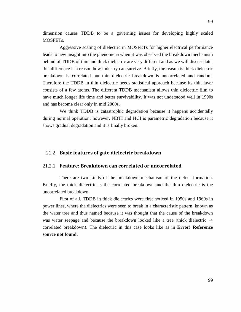
First of all, TDDB in thick dielectrics were first noticed in 1950s and 1960s in
power lines, where the dielectrics were seen to break in a characteristic pattern, known as
the water tree and thus named because it was thought that the cause of the breakdown
was water seepage and because the breakdown looked like a tree (thick dielectric →
correlated breakdown). The dielectric in this case looks like as in Error! Reference
source not found.
100
100
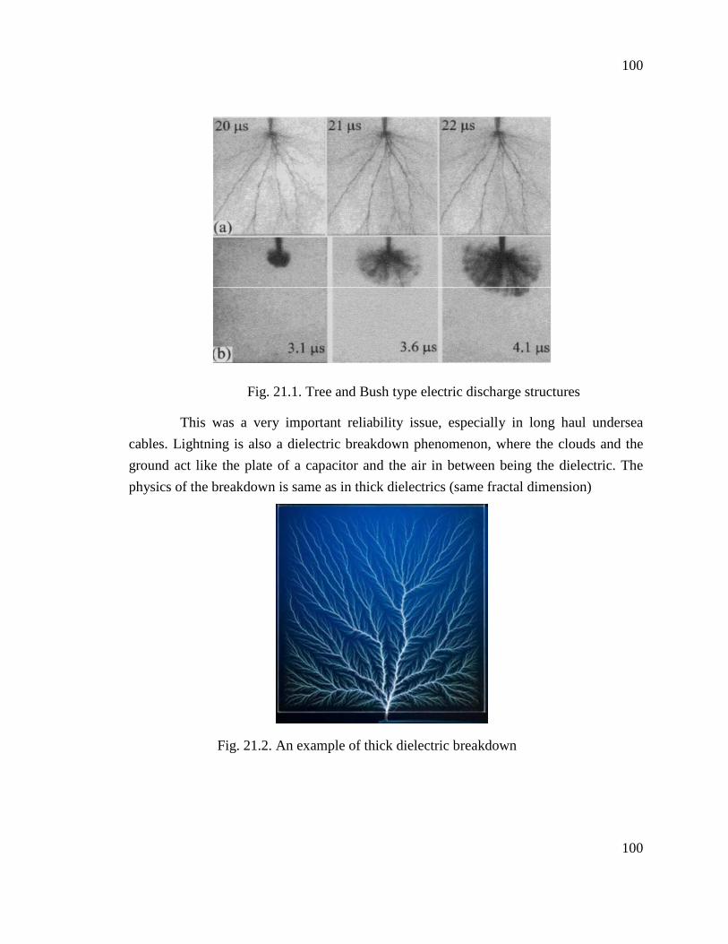
This was a very important reliability issue, especially in long haul undersea
cables. Lightning is also a dielectric breakdown phenomenon, where the clouds and the
ground act like the plate of a capacitor and the air in between being the dielectric. The
physics of the breakdown is same as in thick dielectrics (same fractal dimension)
Fig. 21.1. Tree and Bush type electric discharge structures
Fig. 21.2. An example of thick dielectric breakdown
101
101
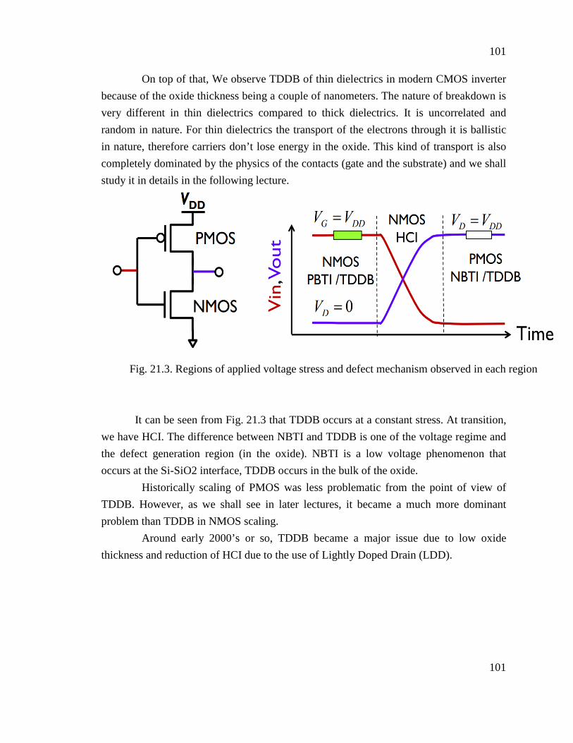
On top of that, We observe TDDB of thin dielectrics in modern CMOS inverter
because of the oxide thickness being a couple of nanometers. The nature of breakdown is
very different in thin dielectrics compared to thick dielectrics. It is uncorrelated and
random in nature. For thin dielectrics the transport of the electrons through it is ballistic
in nature, therefore carriers don’t lose energy in the oxide. This kind of transport is also
completely dominated by the physics of the contacts (gate and the substrate) and we shall
study it in details in the following lecture.
It can be seen from Fig. 21.3 that TDDB occurs at a constant stress. At transition,
we have HCI. The difference between NBTI and TDDB is one of the voltage regime and
the defect generation region (in the oxide). NBTI is a low voltage phenomenon that
occurs at the Si-SiO2 interface, TDDB occurs in the bulk of the oxide.
Historically scaling of PMOS was less problematic from the point of view of
TDDB. However, as we shall see in later lectures, it became a much more dominant
problem than TDDB in NMOS scaling.
Around early 2000’s or so, TDDB became a major issue due to low oxide
thickness and reduction of HCI due to the use of Lightly Doped Drain (LDD).
Fig. 21.3. Regions of applied voltage stress and defect mechanism observed in each region
102
102
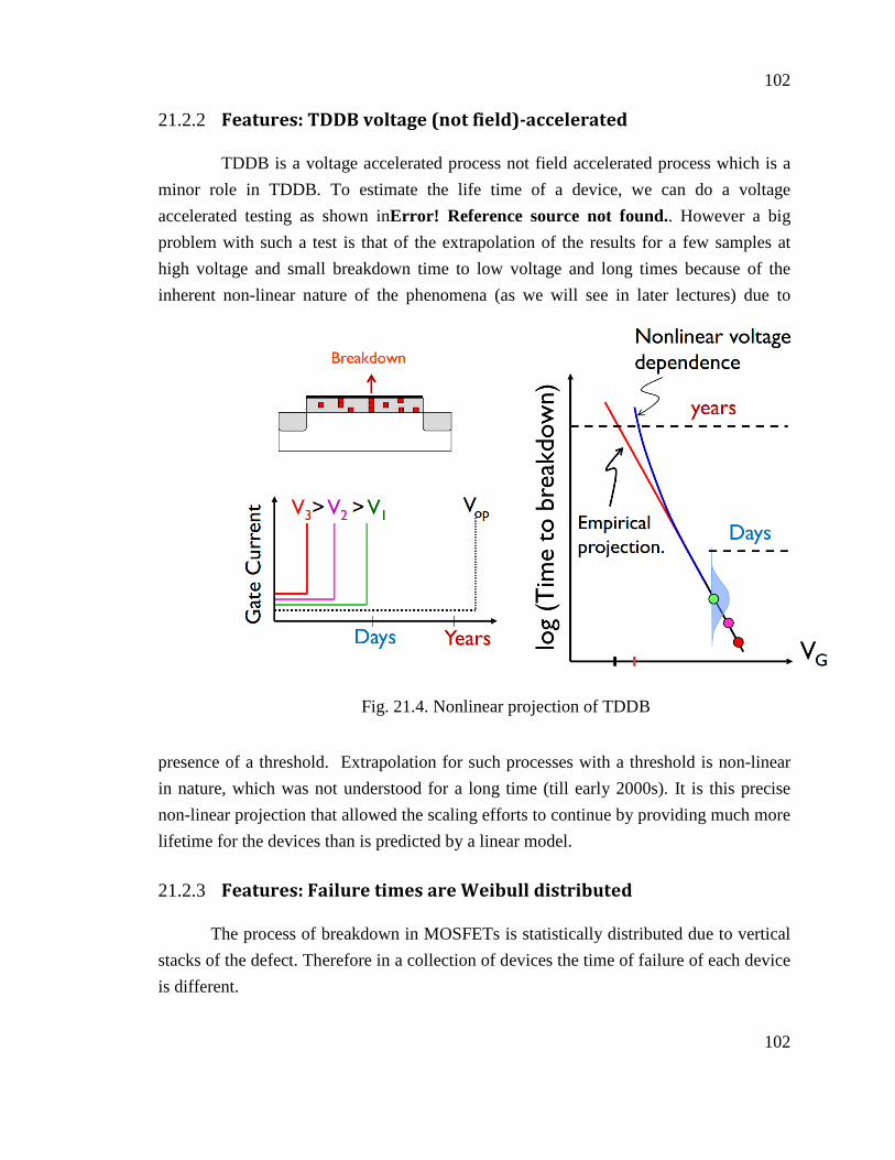
21.2.2 Features: TDDB voltage (not field)-accelerated
TDDB is a voltage accelerated process not field accelerated process which is a
minor role in TDDB. To estimate the life time of a device, we can do a voltage
accelerated testing as shown inError! Reference source not found.. However a big
problem with such a test is that of the extrapolation of the results for a few samples at
high voltage and small breakdown time to low voltage and long times because of the
inherent non-linear nature of the phenomena (as we will see in later lectures) due to
presence of a threshold. Extrapolation for such processes with a threshold is non-linear
in nature, which was not understood for a long time (till early 2000s). It is this precise
non-linear projection that allowed the scaling efforts to continue by providing much more
lifetime for the devices than is predicted by a linear model.
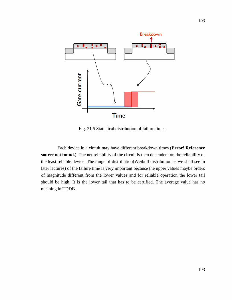
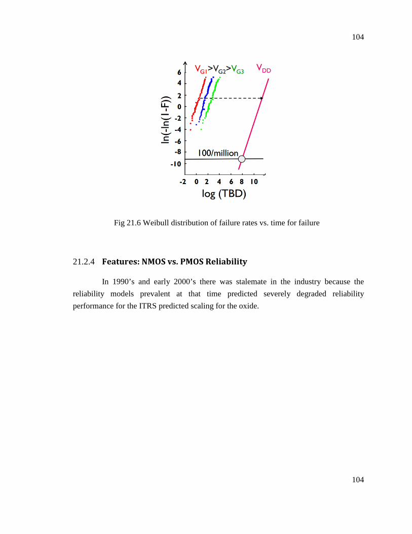
21.2.3 Features: Failure times are Weibull distributed
The process of breakdown in MOSFETs is statistically distributed due to vertical
stacks of the defect. Therefore in a collection of devices the time of failure of each device
is different.
Fig. 21.4. Nonlinear projection of TDDB
103
103
Each device in a circuit may have different breakdown times (Error! Reference
source not found.). The net reliability of the circuit is then dependent on the reliability of
the least reliable device. The range of distribution(Weibull distribution as we shall see in
later lectures) of the failure time is very important because the upper values maybe orders
of magnitude different from the lower values and for reliable operation the lower tail
should be high. It is the lower tail that has to be certified. The average value has no
meaning in TDDB.
Fig. 21.5 Statistical distribution of failure times
104
104
21.2.4 Features: NMOS vs. PMOS Reliability
In 1990’s and early 2000’s there was stalemate in the industry because the
reliability models prevalent at that time predicted severely degraded reliability
performance for the ITRS predicted scaling for the oxide.
Fig 21.6 Weibull distribution of failure rates vs. time for failure
105
105
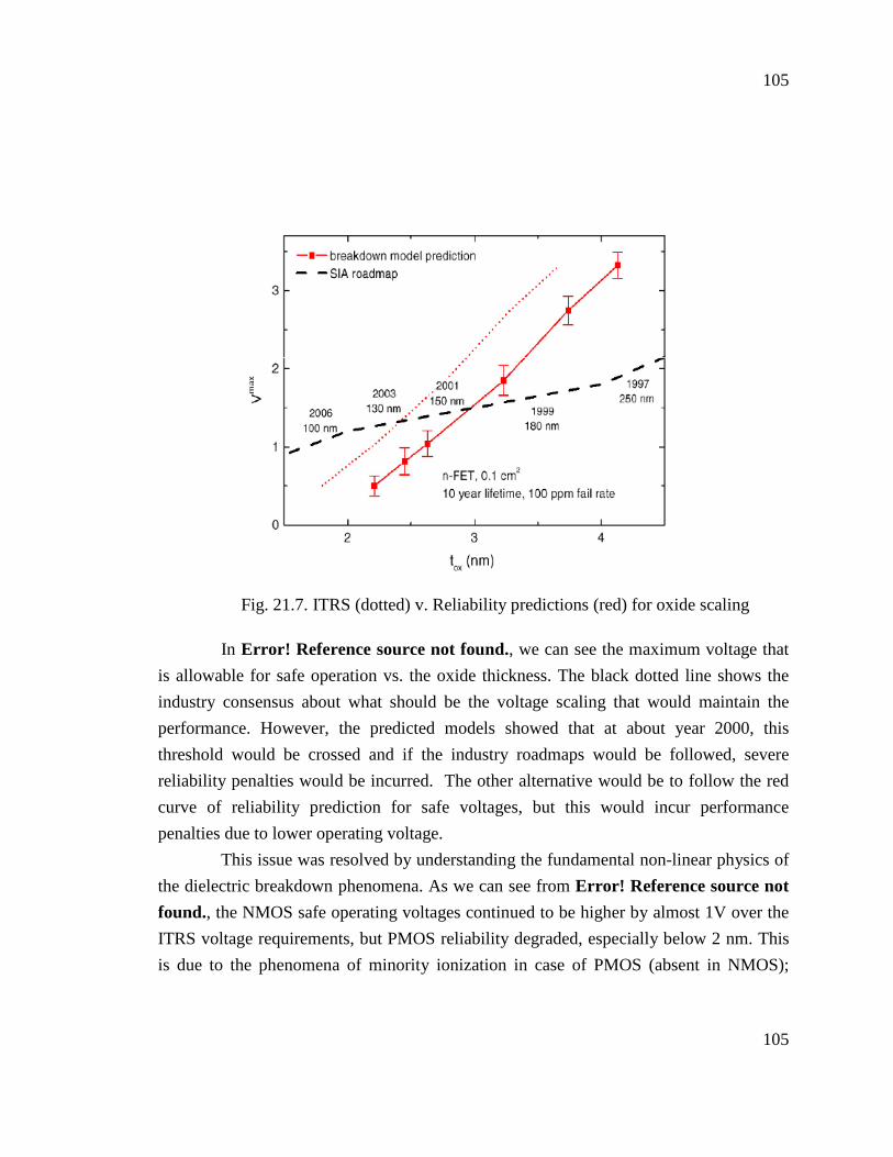
In Error! Reference source not found., we can see the maximum voltage that
is allowable for safe operation vs. the oxide thickness. The black dotted line shows the
industry consensus about what should be the voltage scaling that would maintain the
performance. However, the predicted models showed that at about year 2000, this
threshold would be crossed and if the industry roadmaps would be followed, severe
reliability penalties would be incurred. The other alternative would be to follow the red
curve of reliability prediction for safe voltages, but this would incur performance
penalties due to lower operating voltage.
This issue was resolved by understanding the fundamental non-linear physics of
the dielectric breakdown phenomena. As we can see from Error! Reference source not
found., the NMOS safe operating voltages continued to be higher by almost 1V over the
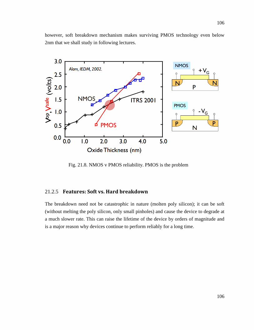
ITRS voltage requirements, but PMOS reliability degraded, especially below 2 nm. This
is due to the phenomena of minority ionization in case of PMOS (absent in NMOS);
Fig. 21.7. ITRS (dotted) v. Reliability predictions (red) for oxide scaling
106
106
however, soft breakdown mechanism makes surviving PMOS technology even below
2nm that we shall study in following lectures.
21.2.5 Features: Soft vs. Hard breakdown
The breakdown need not be catastrophic in nature (molten poly silicon); it can be soft
(without melting the poly silicon, only small pinholes) and cause the device to degrade at
a much slower rate. This can raise the lifetime of the device by orders of magnitude and
is a major reason why devices continue to perform reliably for a long time.
Fig. 21.8. NMOS v PMOS reliability. PMOS is the problem
107
107
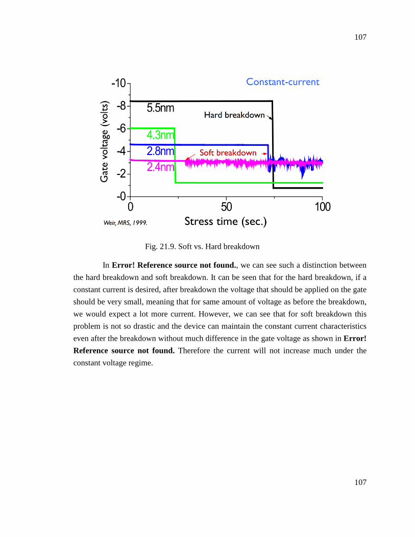
In Error! Reference source not found., we can see such a distinction between
the hard breakdown and soft breakdown. It can be seen that for the hard breakdown, if a
constant current is desired, after breakdown the voltage that should be applied on the gate
should be very small, meaning that for same amount of voltage as before the breakdown,
we would expect a lot more current. However, we can see that for soft breakdown this
problem is not so drastic and the device can maintain the constant current characteristics
even after the breakdown without much difference in the gate voltage as shown in Error!
Reference source not found. Therefore the current will not increase much under the
constant voltage regime.
Fig. 21.9. Soft vs. Hard breakdown
108
108
21.3 Physical characterization of breakdown spot
TDDB can cause significant damage to the device. It can melt the silicon and
make it go through the oxide into the poly silicon gate and eventually it reaches to source
drain contact. Following figures describes various breakdown spots.
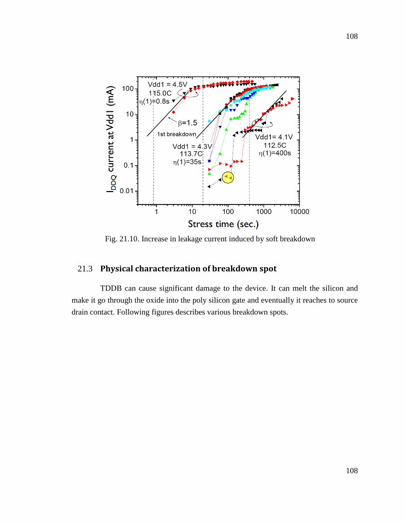
Fig. 21.10. Increase in leakage current induced by soft breakdown
109
109
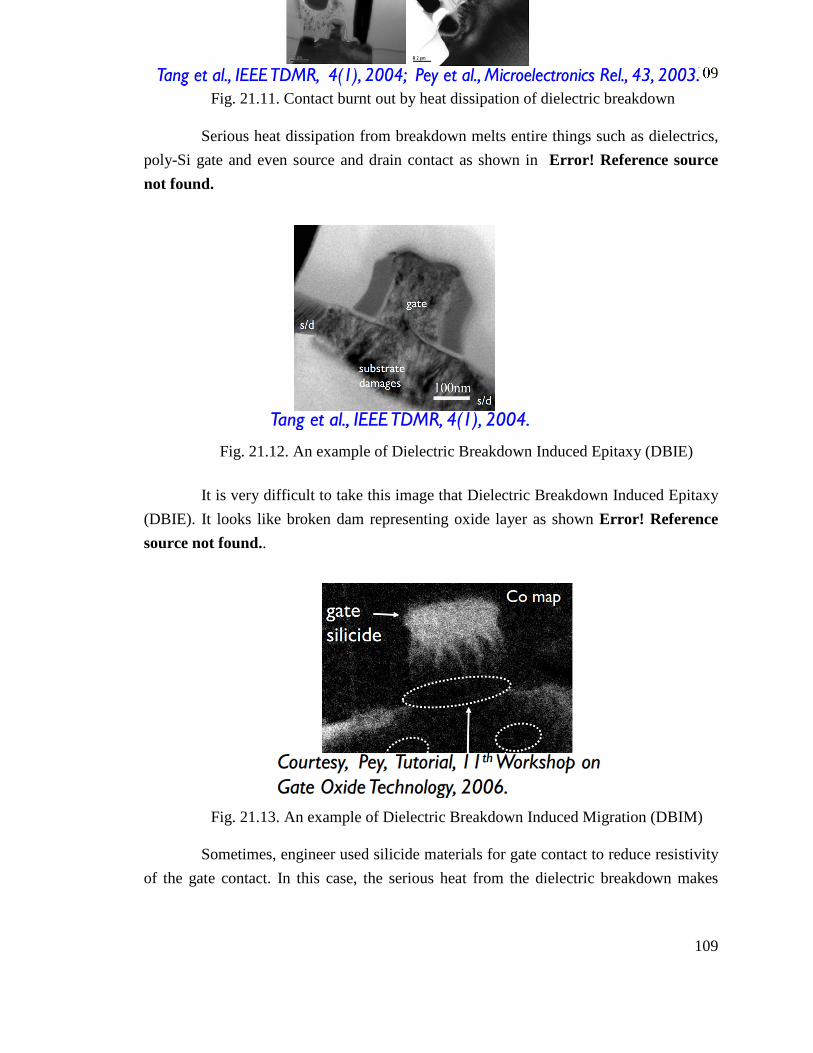
Serious heat dissipation from breakdown melts entire things such as dielectrics,
poly-Si gate and even source and drain contact as shown in Error! Reference source
not found.
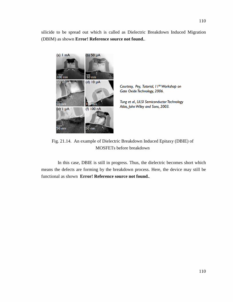
It is very difficult to take this image that Dielectric Breakdown Induced Epitaxy
(DBIE). It looks like broken dam representing oxide layer as shown Error! Reference
source not found..
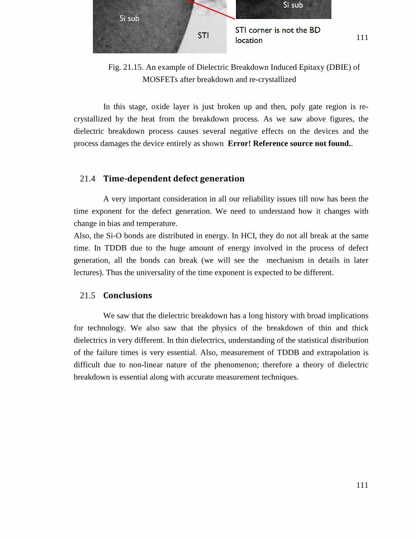
Sometimes, engineer used silicide materials for gate contact to reduce resistivity
of the gate contact. In this case, the serious heat from the dielectric breakdown makes
Fig. 21.11. Contact burnt out by heat dissipation of dielectric breakdown
Fig. 21.12. An example of Dielectric Breakdown Induced Epitaxy (DBIE)
Fig. 21.13. An example of Dielectric Breakdown Induced Migration (DBIM)
110
110
silicide to be spread out which is called as Dielectric Breakdown Induced Migration
(DBIM) as shown Error! Reference source not found..
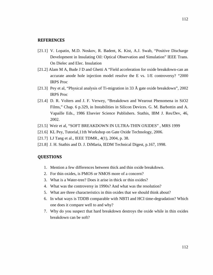
In this case, DBIE is still in progress. Thus, the dielectric becomes short which
means the defects are forming by the breakdown process. Here, the device may still be
functional as shown Error! Reference source not found..
Fig. 21.14. An example of Dielectric Breakdown Induced Epitaxy (DBIE) of
MOSFETs before breakdown
111
111
In this stage, oxide layer is just broken up and then, poly gate region is re-
crystallized by the heat from the breakdown process. As we saw above figures, the
dielectric breakdown process causes several negative effects on the devices and the
process damages the device entirely as shown Error! Reference source not found..
21.4 Time-dependent defect generation
A very important consideration in all our reliability issues till now has been the
time exponent for the defect generation. We need to understand how it changes with
change in bias and temperature.
Also, the Si-O bonds are distributed in energy. In HCI, they do not all break at the same
time. In TDDB due to the huge amount of energy involved in the process of defect
generation, all the bonds can break (we will see the mechanism in details in later
lectures). Thus the universality of the time exponent is expected to be different.
21.5 Conclusions
We saw that the dielectric breakdown has a long history with broad implications
for technology. We also saw that the physics of the breakdown of thin and thick
dielectrics in very different. In thin dielectrics, understanding of the statistical distribution
of the failure times is very essential. Also, measurement of TDDB and extrapolation is
difficult due to non-linear nature of the phenomenon; therefore a theory of dielectric
breakdown is essential along with accurate measurement techniques.
Fig. 21.15. An example of Dielectric Breakdown Induced Epitaxy (DBIE) of
MOSFETs after breakdown and re-crystallized
112
112
REFERENCES
[21.1] V. Lopatin, M.D. Noskov, R. Badent, K. Kist, A.J. Swab, “Positive Discharge
Development in Insulating Oil: Optical Observation and Simulation” IEEE Trans.
On Dielec and Elec. Insulation
[21.2] Alam M A, Bude J D and Ghetti A “Field acceleration for oxide breakdown-can an
accurate anode hole injection model resolve the E vs. 1/E controversy? “2000
IRPS Proc
[21.3] Pey et al, “Physical analysis of Ti-migration in 33 Å gate oxide breakdown”, 2002
IRPS Proc
[21.4] D. R. Volters and J. F. Verwey, “Breakdown and Wearout Phenomena in SiO2
Films,” Chap. 6 p.329, in Instabilities in Silicon Devices. G. M. Barbottin and A.
Vapaille Eds., 1986 Elsevier Science Publishers. Stathis, IBM J. Res/Dev, 46,
2002.
[21.5] Weir et al, “SOFT BREAKDOWN IN ULTRA-THIN OXIDES” , MRS 1999
[21.6] KL Pey, Tutorial,11th Workshop on Gate Oxide Technology, 2006.
[21.7] LJ Tang et al., IEEE TDMR., 4(1), 2004, p. 38.
[21.8] J. H. Stathis and D. J. DiMaria, IEDM Technical Digest, p.167, 1998.
QUESTIONS
1. Mention a few differences between thick and thin oxide breakdown.
2. For thin oxides, is PMOS or NMOS more of a concern?
3. What is a Water-tree? Does it arise in thick or thin oxides?
4. What was the controversy in 1990s? And what was the resolution?
5. What are three characteristics in thin oxides that we should think about?
6. In what ways is TDDB comparable with NBTI and HCI time-degradation? Which
one does it compare well to and why?
7. Why do you suspect that hard breakdown destroys the oxide while in thin oxides
breakdown can be soft?