
Unidad 1 Respuesta en Alta y Baja Frecuencia Con Amp. BJT y FET
Upload
jessica-hamiltonCategory
view
221download
3
CHAPTER 4CHAPTER 4
1
POWER AMPLIFIERPOWER AMPLIFIER

Outcome of Chapter 4Outcome of Chapter 4
Ability to perform simple DESIGN and EVALUATE A, B and AB classes of BJT and FET amplifiers, in terms of their frequency response, equivalent circuit, termal management (power dissipation) and gain.
2
OutlineOutline
3
Introduction
Concept of Power Amplifier
Power Amplifier Classification
BJTs/ MOSFETs Power Amplifier
Class A Power Amplifier

IntroductionIntroductionPower amplifiers are used to deliver a relatively high
amount of power, usually to a low resistance load. Typical load values range from 300W (for transmission
antennas) to 8W (for audio speaker). Although these load values do not cover every
possibility, they do illustrate the fact that power amplifiers usually drive low-resistance loads.
Typical output power rating of a power amplifier will be 1W or higher.
Ideal power amplifier will deliver 100% of the power it draws from the supply to load. In practice, this can never occur.
The reason for this is the fact that the components in the amplifier will all dissipate some of the power that is being drawn form the supply.
4
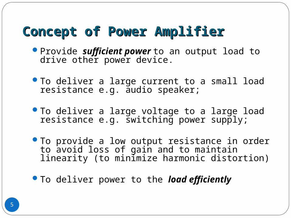
Concept of Power AmplifierConcept of Power Amplifier
5
Provide sufficient power to an output load to drive other power device.
To deliver a large current to a small load resistance e.g. audio speaker;
To deliver a large voltage to a large load resistance e.g. switching power supply;
To provide a low output resistance in order to avoid loss of gain and to maintain linearity (to minimize harmonic distortion)
To deliver power to the load efficiently

6
Power Amplifier Power Power Amplifier Power DissipationDissipation
P1 = I12R1
P2 = I22R2
ICQRC
RE
R1
R2
VCC
I1
I2
ICC
PC = ICQ2 RC
PT = ITQ2 RT
PE = IEQ2 RE
IEQ
The total amount of power being dissipated by the amplifier, Ptot , is
Ptot = P1 + P2 + PC + PT + PE
The difference between this total value and the total power being drawn from the supply is the power that actually goes to the load – i.e. output power.

7
Power Amplifier Efficiency Power Amplifier Efficiency A figure of merit for the power amplifier is its
efficiency, .
Efficiency ( of an amplifier is defined as the ratio of ac output power (power delivered to load) to dc input power .
By formula :
As we will see, certain amplifier configurations have much higher efficiency ratings than others.
This is primary consideration when deciding which type of power amplifier to use for a specific application.
%100)(
)(%100
dcP
acP
powerinputdc
poweroutputac
i
o

Power Amplifiers Classification Power Amplifiers Classification
8
Class A - The transistor conducts during the whole cycle of sinusoidal input signal
Class B - The transistor conducts during one-half cycle of input signal
Class AB - The transistor conducts for slightly more than half a cycle of input signal
Class C - The transistor conducts for less than half a cycle of input signal

9
Efficiency RatingsEfficiency Ratings The maximum theoretical efficiency
ratings of class-A, B, and C amplifiers are:
Amplifier Maximum Theoretical Efficiency, max
Class A 25%
Class B 78.5%
Class C 99%

BJT Power AmplifierBJT Power Amplifier
Comparison of the characteristics and maximum ratings of a small-signal and power BJT
ParameterSmall-signal BJT
(2N2222A)Power BJT(2N3055)
Power BJT(2N6078)
VCE (max) (V) 40 60 250
IC (max) (A) 0.8 15 7
PD (max) (W) 1.2 115 45
35 – 100 5 – 20 12 – 70
fT (MHz) 300 0.8 1
10
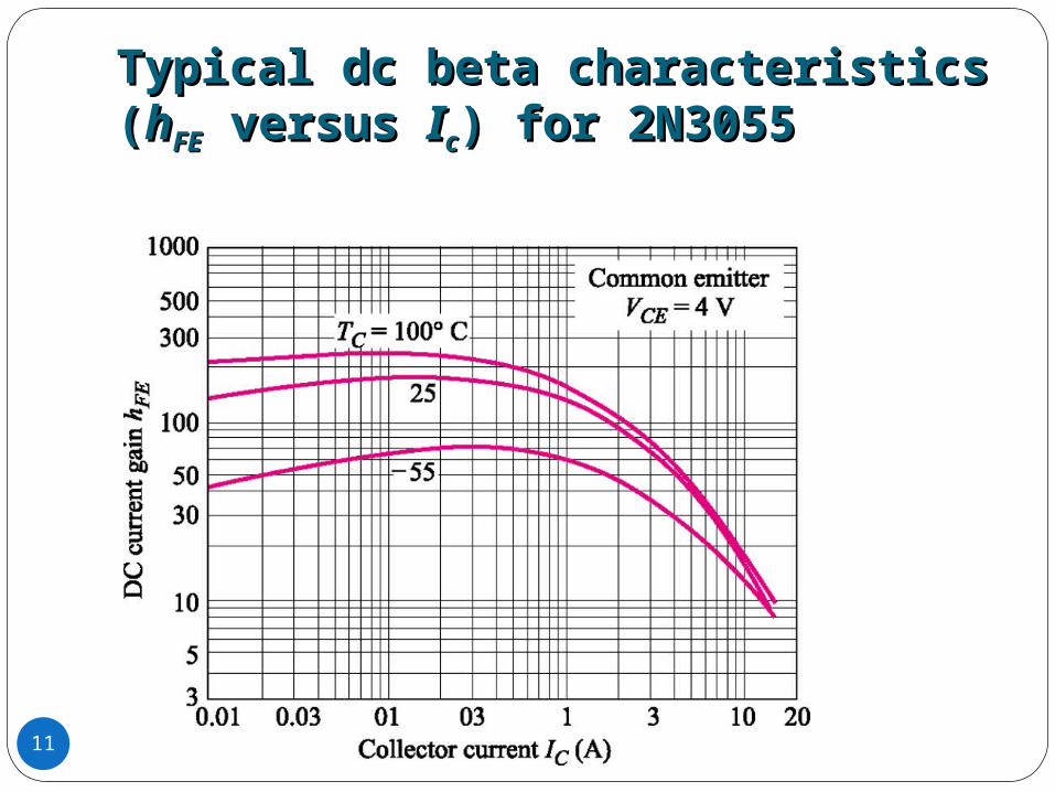
Typical dc beta characteristics Typical dc beta characteristics ((hhFEFE versus versus IIcc) for 2N3055) for 2N3055
11

BJTs Power AmplifierBJTs Power Amplifier
12
Current gain is smaller in power amplifier BJT. The gain depends on IC and temperature may be
related to the following:
maximum current that connecting wires can handle
at which current gain falls below a stated value current which leads to maximum power
dissipation. maximum voltage limitation associated with
avalanche breakdown in reverse-biased collector-base junction.
second breakdown in BJT operating at high voltage and current.

13
VCE(sus) =115 volt at which these curve merge and the minimum voltage necessary to sustain the transistor in breakdown.
The breakdown voltage, VCE0 ~130 volt when the base terminal is open circuited, IB=0

Instantaneous power dissipation
The average power over one cycle
The maximum rated power,
CCEBBECCEQ ivivivp
T
CCEQ dtivT
P0
1
14
CCET IVP

MOSFETs Power AmplifierMOSFETs Power AmplifierCharacteristic of two power MOSFETs
ParameterPower
MOSFET2N6757
Power MOSFET2N6792
VDS (max) (V) 150 400
ID (max) (A) (at T = 25C) 8 2
PD (max) (W) 75 20
15
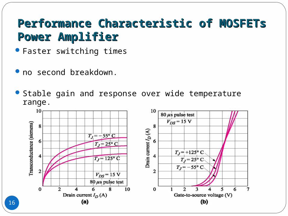
Performance Characteristic of MOSFETs Performance Characteristic of MOSFETs Power AmplifierPower Amplifier
16
Faster switching times
no second breakdown.
Stable gain and response over wide temperature range.

17
Class A AmplifierClass A Amplifier
output waveform same shape input waveform + phase shift.
The collector current is nonzero 100% of the time. inefficient, since even with zero input signal, ICQ is nonzero(i.e. transistor dissipates power in the rest, or quiescent, condition)
vin voutAv
18
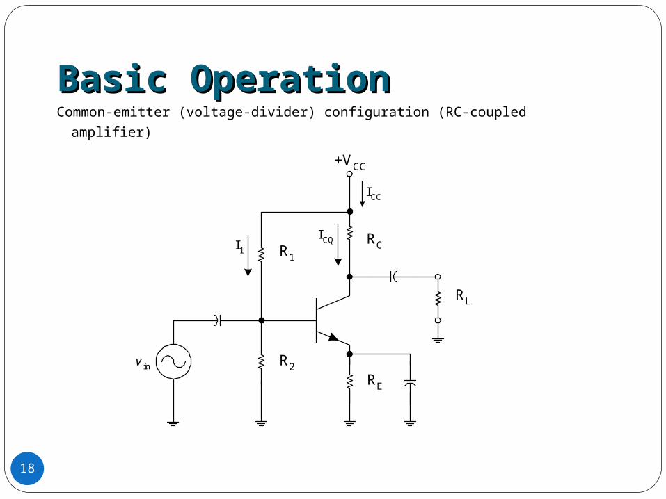
Basic OperationBasic OperationCommon-emitter (voltage-divider) configuration (RC-coupled amplifier)
RC
+VCC
RE
R1
R2
RL
v in
ICQI1
ICC

Typical Characteristic Curves for Typical Characteristic Curves for Class A OperationClass A Operation
19
Configuration : No inductor @ transformer are used
(a) Common-emitter amplifier,
(b) dc load line (the Q point is at centre of the load line)
(c) instantaneous power dissipation versus time in the transistor

20
DC Input PowerDC Input Power
RC
+VCC
RE
R1
R2
RL
v in
ICQI1
ICCThe total dc power, Pi(dc) , that an
amplifier draws from the power supply :
CCCCiIVdcP )(
1III
CQCC
CQCCII )(
1II
CQ
CQCCiIVdcP )(
Note that this equation is valid for most amplifier power analyses. We can rewrite for the above equation for the ideal amplifier as
CQCEQiIVdcP 2)(

21
AC Output Power AC Output Power
R1//R2
vcevin
vo
ic
RC//RLrC
AC output (or load) power, Po(ac)
Above equations can be used to calculate the maximum possible value of ac load power. HOW??
L
rmso
rmsormsco R
vviacP
2
)(
)()()(
Disadvantage of using class-A amplifiers is the fact that their efficiency ratings are so low, max 25% .
Why?? A majority of the power that is drawn from the supply by a class-A amplifier is used up by the amplifier itself.

22
IC(mA)
VCE
VCE(off) = VCC
IC(sat) = VCC/(RC+RE)
DC Load LineIC
VCE
IC(sat) = ICQ + (VCEQ/rC)
VCE(off) = VCEQ + ICQrC
ac load line
IC
VCE
Q - point
ac load line
dc load line
L
PP
CQCEQ
CQCEQ
o R
VIV
IVacP
82
1
22)(
2
%25%10022
1
%100)(
)( CQCEQ
CQCEQ
dci
aco
IV
IV
P
P

23
LimitationLimitation
24
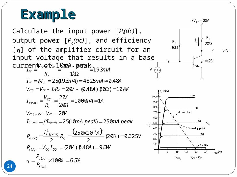
ExampleExampleCalculate the input power [Pi(dc)], output power
[Po(ac)], and efficiency [] of the amplifier circuit for
an input voltage that results in a base current of 10mA peak.
RCRB
+VCC = 20V
IC
Vi
25
20k1
Vo
%5.6%100
6.9)48.0)(20(
625.0)20(2
10250
2
250)10(25
20
1100020
20
4.10)20)(48.0(20
48.05.482)3.19(25
3.191
7.020
)(
)(
)(
232)(
)(
)(
)()(
)(
dci
aco
CQCCdci
CpeakC
aco
C
CCsatc
B
P
P
WAVIVP
WA
RI
P
peakmApeakmAII
VVV
AmAV
R
VI
VAVRIVV
AmAmAII
mAk
VV
R
VVI
peakbpeakC
CCcutoffCE
CCCCCEQ
CQ
B
BECC
BQ

ExampleExample
25
The common source circuit parameters are VDD=10V, RD=5kΩ and the transistor parameters are Kn=1mA/V2, VTN=1V and =0.
Assume the output voltage swing is limited to the range between the transition point and vDS=9V to minimize nonlinear distortion.
Calculate the actual efficiency of a class A output stage.
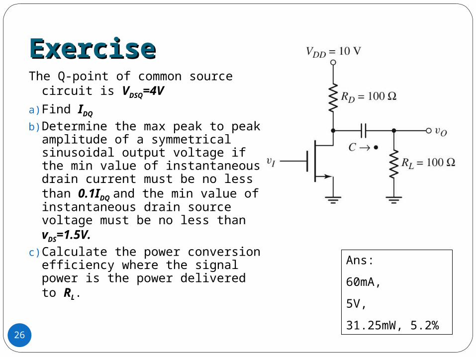
ExerciseExercise
26
The Q-point of common source circuit is VDSQ=4V
a) Find IDQ
b) Determine the max peak to peak amplitude of a symmetrical sinusoidal output voltage if the min value of instantaneous drain current must be no less than 0.1IDQ and the min value of instantaneous drain source voltage must be no less than vDS=1.5V.
c) Calculate the power conversion efficiency where the signal power is the power delivered to RL.
Ans:
60mA,
5V,
31.25mW, 5.2%

Design of Class A C-E Design of Class A C-E AmplifierAmplifierTo find R1, R2, RE, RC use the DC analysis and
design formula;
To find Zi, Zo, Av, Ai use AC analysis (without loading effect)
To find Zi, Zo, Avs, Ai use AC analysis (with loading effect if have Ri and RL
27
LC
CQC
ECCCQ
CCEQ
II
II
RR
VV
VV
10; Rhave If
sheet.data in given10
;2
;10
L
2

Example & ExerciseExample & Exercise
Will be given in our class.
28

Class B Power AmplifierClass B Power Amplifier Consists of complementary pair electronic devices
One conducts for one half cycle of the input signal and the other conducts for another half of the input signal
When the input is zero, both devices are off, the bias currents are zero and the output is zero.
Ideal voltage gain is unity
29

For input larger than zero, A turn ON and supplies current to the load.
For input less than zero, B turn ON and sinks current from the load
30
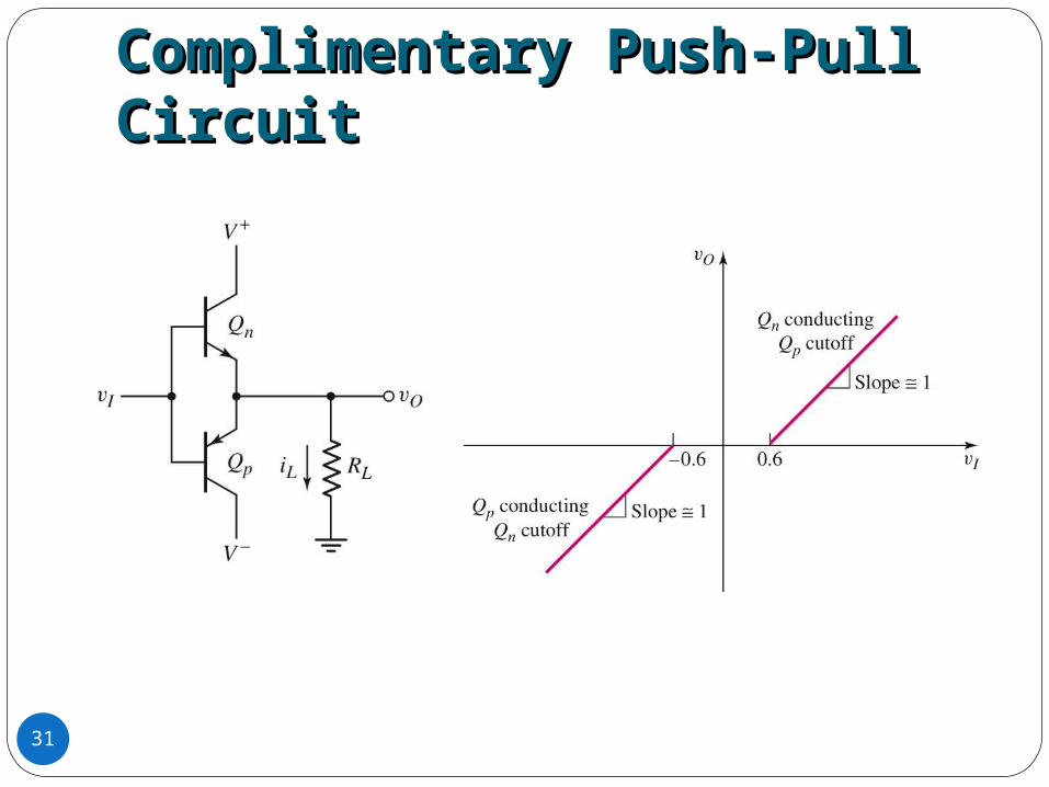
Complimentary Push-Pull CircuitComplimentary Push-Pull Circuit
31

DEAD BAND
CROSSOVER DISTORTION
32
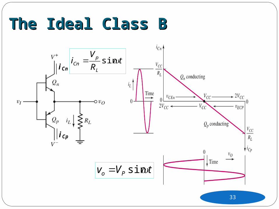
The Ideal Class BThe Ideal Class B
tVv po sin
tR
Vi
L
pCn sin
i Cn
i Cp
tVv Po sin
sin tR
Vi
L
pCn
33

• Maximum possible value of Vp is VCC
• The instantaneous power in Qn is;
tVVv pCCCEn sin
CnCEnQn ivp
t
R
VtVVp
L
ppCCQn sinsin
34
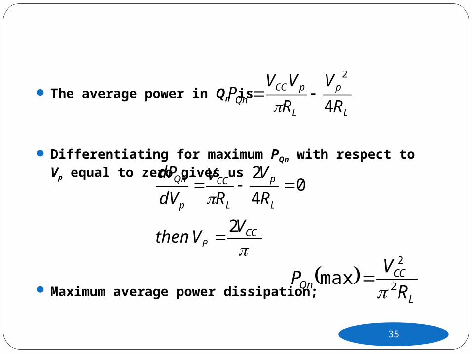
The average power in Qn is
Differentiating for maximum PQn with respect to Vp equal to zero gives us
Maximum average power dissipation;
L
p
L
pCCQn R
V
R
VVP
4
2
L
CCQn R
VP
2
2
max
CCP
L
p
L
CC
p
Qn
VVthen
R
V
R
V
dV
dP
2
04
2
35

The average power delivered to the load is
Power source supplies half sinewave of current,
the average value is;
The total power supplied by the two sources is
L
pS R
VI
L
pL R
VP
2
2
1
L
pCCSCCsS R
VVIVPP
L
pCCSCCS R
VVIVP
22
36

The efficiency is
%5.78785.04
when efficiency maximum
42
2
21
CCP
CC
p
RV
CC
RV
S
L
VV
V
V
VP
P
L
P
L
P
37

Class AB Power AmplifierClass AB Power Amplifier
Small quiescent bias on each output transistor to eliminate crossover distortion
38

Class C Power AmplifierClass C Power Amplifier
39
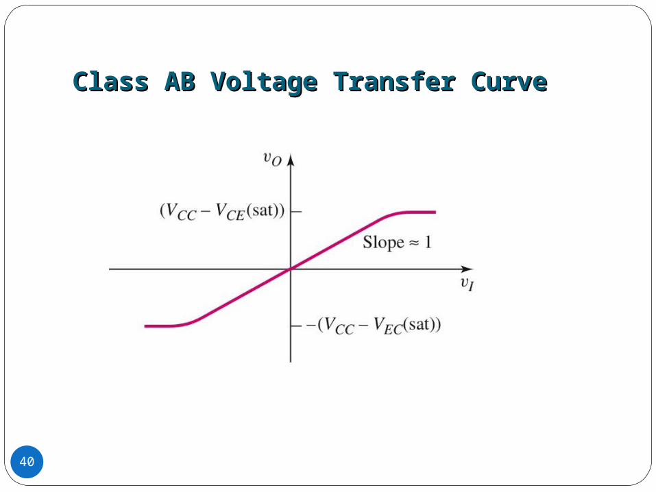
Class AB Voltage Transfer CurveClass AB Voltage Transfer Curve
40
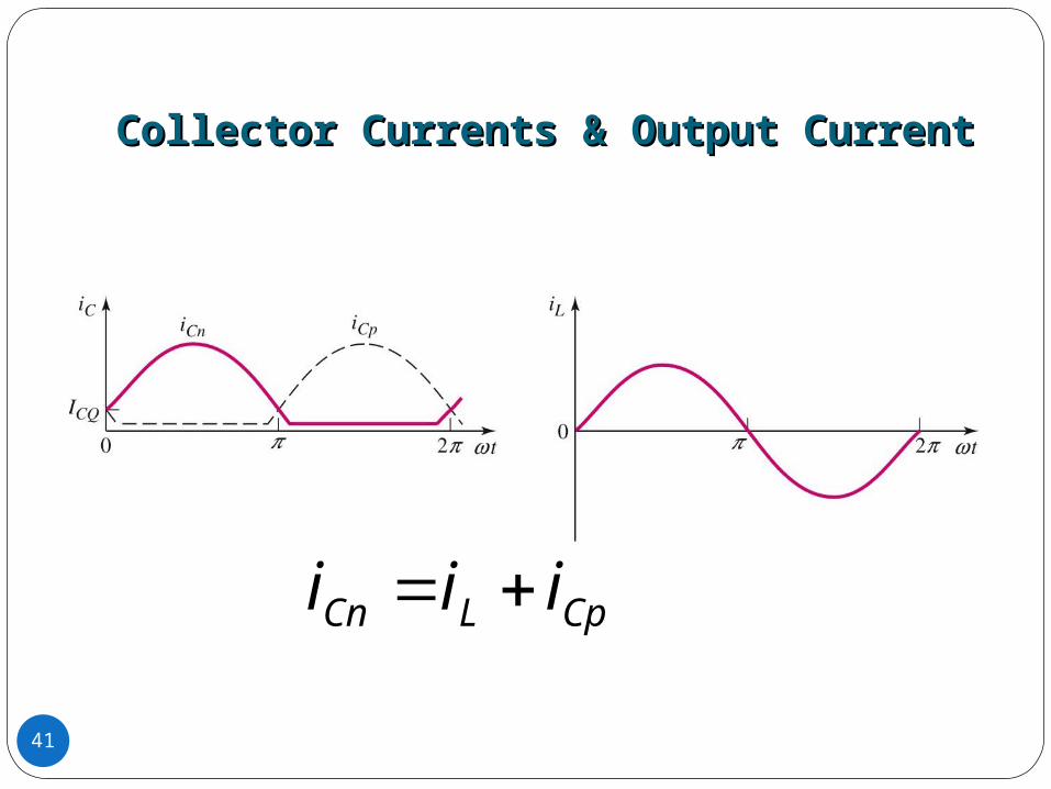
Collector Currents & Output CurrentCollector Currents & Output Current
CpLCn iii
41

ExampleExample
The parameters are VDD=10V, RL=20Ω. The transistor are matched and K=0.2A/V2, VT=1V, IDQ=0.05 when vo=5V.
Determine the required biasing in a MOSFET class AB output stage.
42
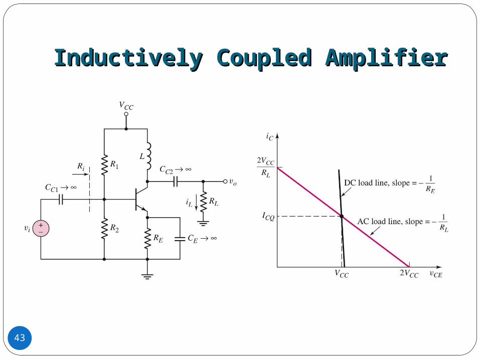
Inductively Coupled AmplifierInductively Coupled Amplifier
43
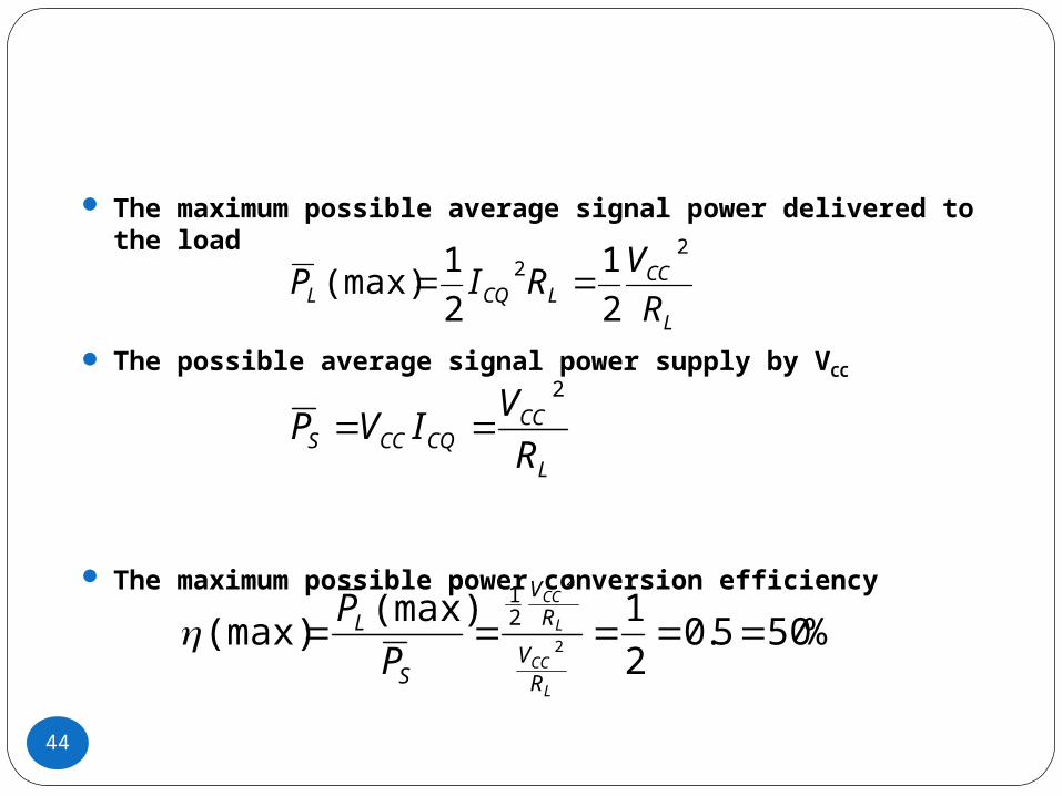
The maximum possible average signal power delivered to the load
The possible average signal power supply by VCC
The maximum possible power conversion efficiency
L
CCLCQL R
VRIP
22
2
1
2
1(max)
L
CCCQCCS R
VIVP
2
%505.02
1(max)(max) 2
2
21
L
CC
L
CC
RV
RV
S
L
P
P
44

Transformer Coupled AmplifierTransformer Coupled Amplifier
45
• The theoretical maximum efficiency of a basic RC-coupled class-A amplifier is limited to 25%.
• In practical circuit, the efficiency is less than 25%.
• Used for output power of about 1 W only.
• Transformer coupling can increase the maximum efficiency to 50%
• Disadvantage of transformer coupling – expensive & bulky.

46
Neglecting transformer resistance and assuming RE is small;
CCCEQ VV

47
a
vvaii CL
12 and
For ideal transformer;
2
1ratioturn N
Na
CLL ai
av
i
vR
/12
21 1
ai
vR
CL
i C
CL i
vR 1' LL RaR 2'

48
Turn ratio is designed for maximum symmetrical swing, hence;
The maximum average power delivered to load equals maximum average power delivered to the primary of the transformer
LCQ
CC
CQ
CCL Ra
I
V
I
VR 2
2
2'
CQCCL IVP2
1max
(VCC and ICQ are maximum possible amplitudes of signal)

49
The average power supplied by the VCC source is;
CQCCS IVP
The maximum possible efficiency is;
%505.0
max
S
L
P
P


![Junction Transistor (Revision with Ques.) · [9 ] BJT FET BJT (bipolar junction transistor ) is the bipolar device FET (field effect transistor) is a uni - polar device Its operation](https://static.fdocuments.net/doc/165x107/5e080e954f3d5f6410302f8e/junction-transistor-revision-with-ques-9-bjt-fet-bjt-bipolar-junction-transistor.jpg)


![[DSE] 2 Amplificacion de pequeña señal con transistores BJT y FET](https://static.fdocuments.net/doc/165x107/5571f19949795947648b6367/dse-2-amplificacion-de-pequena-senal-con-transistores-bjt-y-fet.jpg)