Transistors: BJT, FET and MOSFET
18
TRANSISTORS: BJT, FET AND MOSFET Semiconductor Engineering W A T Mahesh Dananjaya [email protected] ISAAC Intelligent Systems and Advanced Computing
-
Upload
mahesh-dananjaya -
Category
Engineering
-
view
220 -
download
12
Transcript of Transistors: BJT, FET and MOSFET

TRANSISTORS: BJT, FET AND
MOSFET
Semiconductor Engineering
W A T Mahesh Dananjaya [email protected]
ISAAC Intelligent Systems and Advanced Computing

TRANSISTORS: BJT, FET
AND MOSFET
Semiconductor Engineering
ISAAC
Intelligent Systems and Advanced Computing
W A T Mahesh Dananjaya
Department of Electronic and Telecommunication Engineering
University of Moratuwa
Sri Lanka

Contents 1 Semiconductor Engineering .................................................................................................................. 3
1.1 Semiconductors ............................................................................................................................ 3
1.1.1 Extrinsic Semiconductors ...................................................................................................... 3
1.2 Transistors ..................................................................................................................................... 4
1.2.1 Bipolar Junction Transistors (BJT) ......................................................................................... 4
1.2.2 FET (Field Effect Transistor) .................................................................................................. 5
1 Semiconductor Engineering
1.1 Semiconductors
Material that has both conduction and insulation properties are called a semiconductor. As the name
implies the semiconductors are materials of having conductivity between insulators and pure conductors.
Operation of semiconductors is based on the quantum physics and energy band theories. Materials such
as Silicon, Germanium are well known semiconductors.
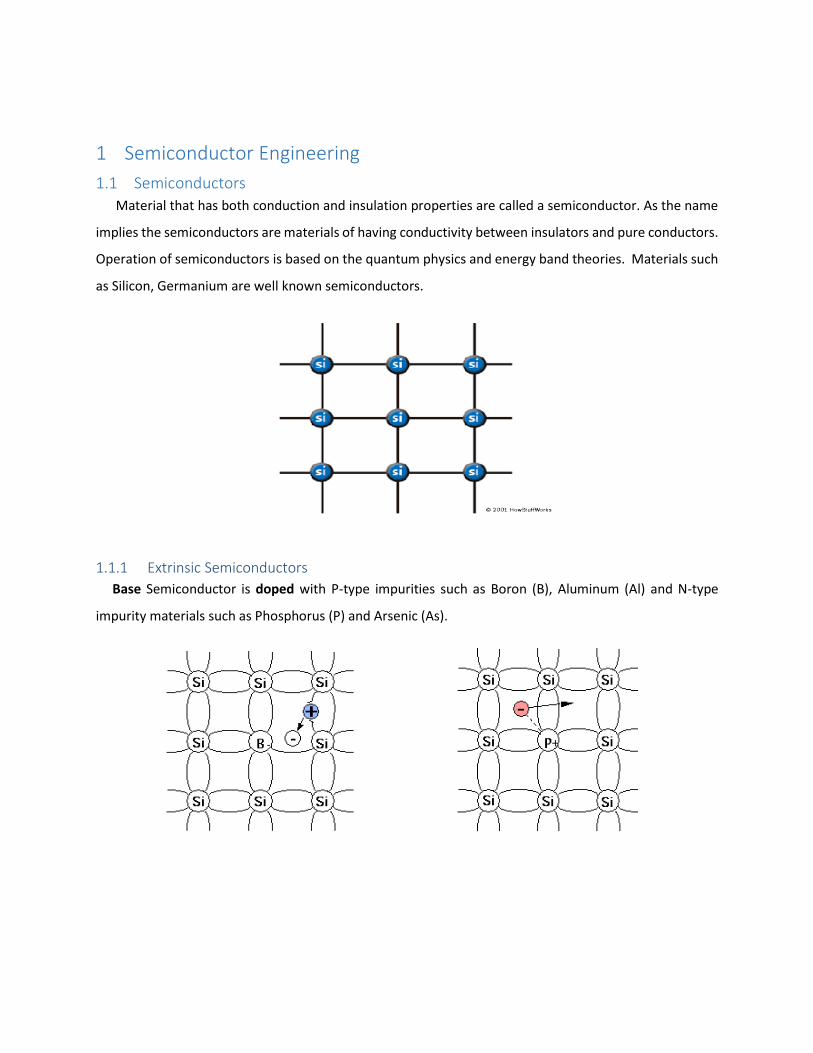
1.1.1 Extrinsic Semiconductors
Base Semiconductor is doped with P-type impurities such as Boron (B), Aluminum (Al) and N-type
impurity materials such as Phosphorus (P) and Arsenic (As).

1.2 Transistors
Transistors are the semiconductor devices which can be used as an electronic switches, amplifiers and
power sources. There are two types of transistors, Bipolar Junction Transistors (BJT) and Field Effect
Transistors (FET).
1.2.1 Bipolar Junction Transistors (BJT)
Bipolar Junction Transistors are relies on the contact and combining of two types of semiconductor for
its operation. BJT can be used as amplifier, switches and oscillators. Operation of BJT involves both
electrons and holes. Uniquely in semiconductors these two type s are originated with the two different
doping of impurities in to base material. Current flow is due to diffusion of charge carriers across the
junction between two regions of different charge concentrations. Electrons are majority charge carriers
in n-type semiconductors, whereas holes are majority charge carriers in p-type semiconductors.
Basically BJTs are consisting of 3 lead called Base, Collector and Emitter. Therefore we can use
characteristics equations and graphs to identify the operation of the BJT.

By controlling the electric field across Base-Emitter junction thus depletion layer we can control the
charged carriers flows between collector and emitter. Above figure shows the operation of NPN transistor.
Characteristics graph of the BJTs are shown here. This will illustrate the operation of NPN transistor. PNP
transistor also works in a similar way.
Transistors are used in three different configurations, common Base, common Collector and common
collector. We are not discussed them here and our aim is to illustrate power of those semiconductor
materials later.
Unipolar Transistors
1.2.2 FET (Field Effect Transistor)
Field Effect Transistor (FET) is one of unipolar transistors that use an electric field to control the shape
and hence the conductivity of a channel of one type of charge carrier in a semiconductor material and
involve single carrier operation. FET are single charged carrier device and FET is consist of an active
channel through which charge carriers, electrons and holes, flow from the source to drain. Source and
drain terminal conducts are connected to the semiconductor through Ohmic contacts. More important
characteristic of this device is that the conductivity of the channel is a function of the potential applied
across the gate and source terminals. There are three leads for FET, gate, source and drain.
Field Effect Transistor (FET) operates as a conducting semiconductor channel with two Ohmic
contacts between semiconductor and metal, the source and the drain, where the amount of charged
carriers the channel is controlled by the third contact, the gate. In the vertical direction the gate channel
and the substrate structure (gate junction) can be regarded as an orthogonal two terminal device, which
is either a MOS structure or a reverse biased rectifying device that controls the mobile charge across the
channel by capacitive coupling (Filed Effect).
Metal Oxide Semiconductor FET (MOSFET), junction gate FET (JFET), Metal Semiconductor
(MESFET), Heterostructure FET (HFET), are types of FETs.
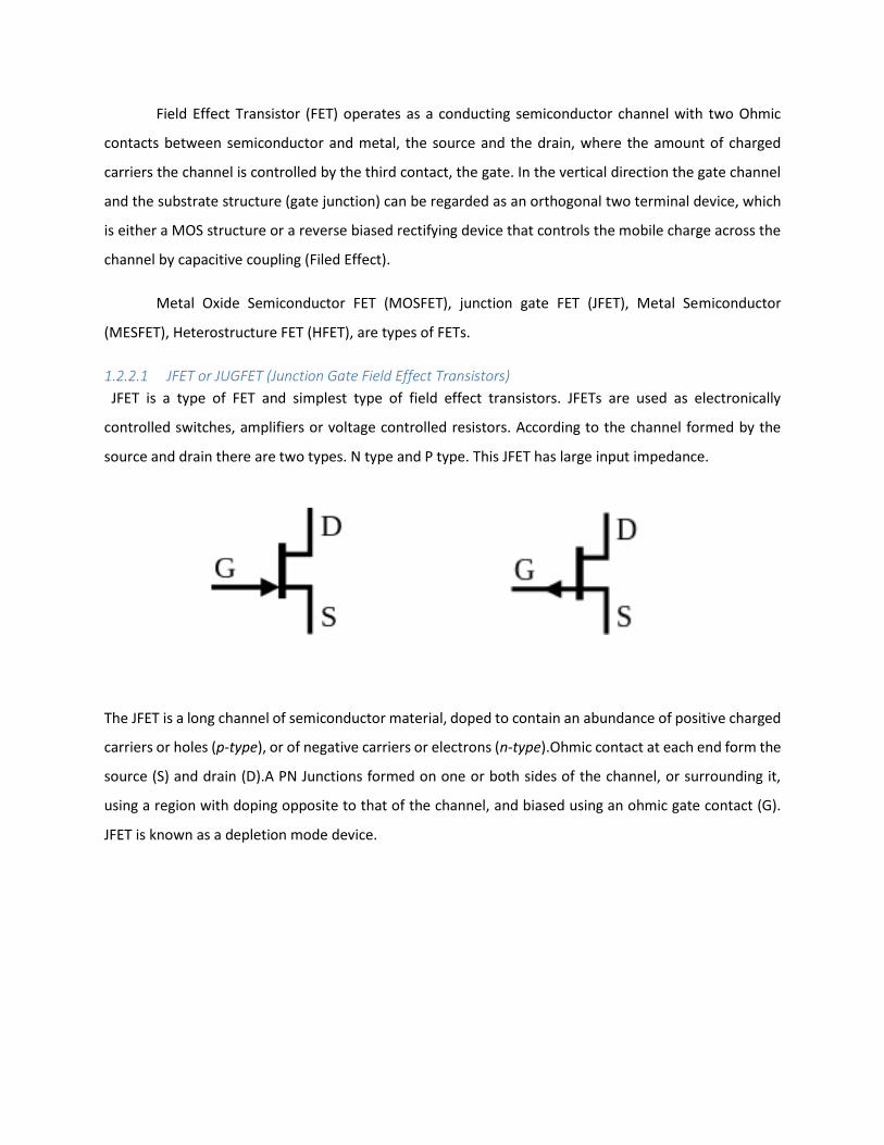
1.2.2.1 JFET or JUGFET (Junction Gate Field Effect Transistors)
JFET is a type of FET and simplest type of field effect transistors. JFETs are used as electronically
controlled switches, amplifiers or voltage controlled resistors. According to the channel formed by the
source and drain there are two types. N type and P type. This JFET has large input impedance.
The JFET is a long channel of semiconductor material, doped to contain an abundance of positive charged
carriers or holes (p-type), or of negative carriers or electrons (n-type).Ohmic contact at each end form the
source (S) and drain (D).A PN Junctions formed on one or both sides of the channel, or surrounding it,
using a region with doping opposite to that of the channel, and biased using an ohmic gate contact (G).
JFET is known as a depletion mode device.
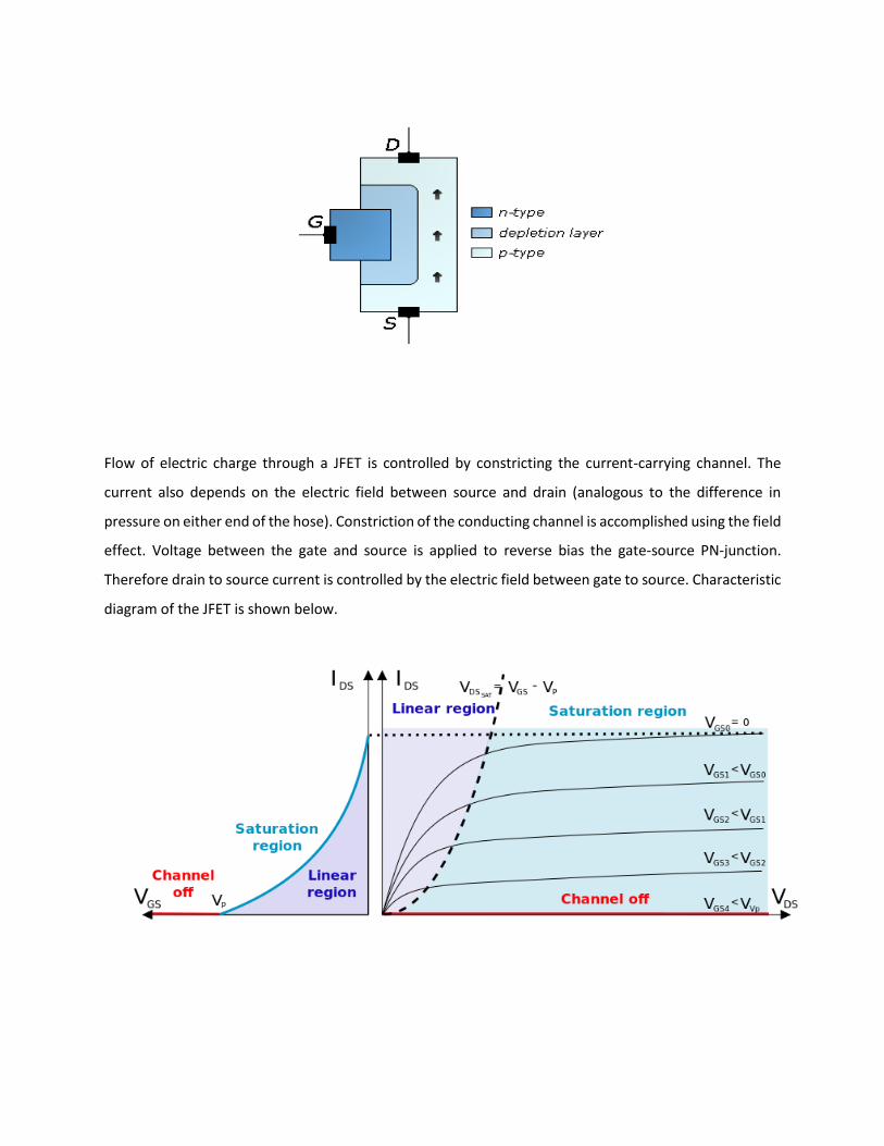
Flow of electric charge through a JFET is controlled by constricting the current-carrying channel. The
current also depends on the electric field between source and drain (analogous to the difference in
pressure on either end of the hose). Constriction of the conducting channel is accomplished using the field
effect. Voltage between the gate and source is applied to reverse bias the gate-source PN-junction.
Therefore drain to source current is controlled by the electric field between gate to source. Characteristic
diagram of the JFET is shown below.

1.2.2.2 MOSFET (Metal Oxide Semiconductor)
The most important FET is the MOSFET. In a silicon MOSFET, the gate contact is separated from
the channel by an insulating silicon dioxide layer. The charge carrier of the conducting channel constitute
an inversion charge, that is, electrons in the case of a P-type substrate in n channel device and holes in
the case of a n-type substrate in P channel devices, induced in the semiconductor at the silicon insulator
interface by the voltage applied across the gate electrodes. The electrons enter and exit the channel at n+
source and drain contacts regarding the N channel MOSFET and at p+ regarding the P channel MOSFET.
1.2.2.2.1 MOS Capacitance
MOSFET is different from the JFET operation because rather than having a reverse biased
rectifying features MOS structure has a MOS capacitor which make a bridge between gate and the
substrate layer. MOS capacitance is the vital part of MOSFET which constitutes the important gate-
channel-substrate structure of the MOSFET. MOS capacitor is a two terminal semiconductor device of
practical interest in its own right. As shown in the below figure it consist of a metal contact separate from
the semiconductor by a dielectric insulator. An additional Ohmic contact is provided at the semiconductor

substrate. Most of the time MOS structure use doped silicon as the substrate and its native oxide, silicon
oxide as the insulator part.
Because of the
insulator it creates an infinite input impedance, preventing any charged carrier transport across the
dielectric layer when a bias voltage is applied between the metal and the semiconductor. Instead, the
applied voltage will induce charge and counter charges and counter charges in the metal and in the
interface layer of the semiconductor, similar to what we expect in the metal plates of a conventional
parallel plate capacitor. However in the MOS capacitor we may use the applied voltage to control the type
of interface charge we induce in the semiconductor, majority carriers, minority carriers and depletion
charge.
1.2.2.2.2 Basic MOSFET Operation
In the MOSFET an inversion layer at the semiconductor oxide interface acts as a conducting
channel. For example in an n channel MOSFET, the substrate is a p-type silicon and the inversion charge
consist of electrons that form a conducting channel between the n+ ohmic source and the drain contacts.
At DC condition, the depletion region and the neutral substrate provide isolation between devices and
fabricated on the same substrate.

In MOS capacitor, inversion charge can be induced in the channel by applying a suitable gate voltage
relative to other terminals. The onset of strong inversion is defined in terms of a threshold voltage Vt
being applied to the gate electrode relative to the other terminals. In order to assure that the induced
inversion channel extends all the way from source to drain, it is essential that the MOSFET gate structure
either overlaps slightly or align with the edges of these contacts. Self-alignment is preferable since it
minimize the parasitic gate-source and gate-drain capacitances.
1.2.2.2.3 MOSFET- Depletion Mode and Enhancement Mode
So far we have discussed about the paramount importance of the MOSFET to the VLSI technology
and without MOSFETs contribution modern electronic systems consist of VLSI technology and large scale
integration is impossible. MOSFETs are usually capable of voltage gain and signal power gain. In this
section we will try to get some understanding about the MOSFET modes and operations which are very
deeply contribute to the VLSI power architectural analysis. N channel and P channel MOSFETs are the two
basic types of MOSFETs. In n channel MOSFET current is due to the flow of electrons in inversion layer and
in p channel current is due to the flow of holes. There are two modes of MOSFET based on their design
architecture, Depletion mode and Enhancement mode. Due to various reasons such as performance,
power and efficiency enhancement mode is widely used in VLSI designs.

1.2.2.2.4 1.2.2.2.4 P Channel MOSFET
MOSFET which deploy p channel region between source and drain is called p-channel MOSFET. Usually
it’s a four terminal device gate, source, drain and substrate or body. Mostly substrate lead is connected
with source lead. Drain and the source are heavily doped with p type impurities thus called p+ regions and
substrate is a doped n-type region. Current flow due to flow of positively charged holes that’s why it’s
called p channel MOSFET.
Depletion Mode: There is a p-type region beneath the oxide layer thus already has a current flowing path
and already form a junction between n-type substrate materials. Therefore it’s really effects the
characteristic MOSFET.
MOSFET
Enhancement Mode
N Channel P Channel
Depletion Mode
N Channel P Channel

Enhancement Mode: There is no p-type region beneath the insulation part and thus threshold voltage is
higher than the depletion mode type. Weak inversion layer is established by the holes extracted by the
p+ regions such as source and drain and minority carriers of the n type substrate.
When applying negative gate voltage, the electrons present beneath the oxide layer, experiences
repulsive force and they are pushed downwards into the substrate, the depletion region is populated by
the bound positive charges which are associated with the donor atoms. Provided that negative voltage to
the gate attracts holes from p+ source and drain region in to the channel region. Thus the channel is
formed with the holes. Now if we apply a voltage difference between the source and the drain, current is
flowing through the channel. The gate voltage controls the Hole concentration of the channel. Only
different in the enhancement mode and depletion mode is that depletion mode MOSFET already contain
a conduction channel (path) and has inversion layer, but enhancement mode do not have a inversion layer

and thus form a weak inversion layer when negative voltage is supplied to the gate by extracting p (holes)
from p+ regions. Thus compose a conduction channel and when gate to source voltage exceeds the
threshold, conduction happens from source to drain if we provide a drain to source voltage.
Characteristic curves of P channel MOSFET
P channel Enhancement Mode Operation

P Channel Depletion Mode
1.2.2.2.5 1.2.2.2.5 N Channel MOSFET
MOSFET having an n-channel region between source and drain is known as n-channel MOSFET. N
channel MOSFET is also consist with four terminals, source, drain, gate and substrate or body. The drain
and source are heavily doped n+ and the substrate is p-type. The current flows due to flow of the
negatively charged electrons. Thus it is called an n-channel MOSFET.
Depletion Mode: There is a n-type region beneath the oxide layer thus already has a current
flowing path and already form a junction between p-type substrate materials. Therefore it’s really effects
the characteristic MOSFET.

Enhancement Mode: There is no n-type region or channel beneath the insulation part and thus
threshold voltage is higher than the depletion mode type. There is no inversion layer and the weak
inversion layer is established by the holes extracted by the n+ regions such as source and drain and
minority carriers of the p type substrate.
Comparison Curves
JFET MOSFET-Depletion MOSFET-Enhancement

NMOS, PMOS, CMOS
MOS logic is built upon the MOSFET and especially CMOS which is widely used in VLSI designs.
NMOS is N type MOSFET and PMOS is a P type MOSFET. CMOS is the combination of p-type and n-type
which is widely used in VLSI power designs.
CMOS is the combining PMOS and NMOS MOSFETs to design MOS logic. CMOS Inverter is shown below.
Basic Logic Cell
CMOS Inverter

More Information…
ISAAC- Intelligent Systems and Advanced Computing
W A T Mahesh Dananjaya
Department of Electronic and Telecommunication Engineering
Faculty of Engineering,
University of Moratuwa,
Sri Lanka