
,Aiii.°1°.€¦ · effect transistor detracts little from its usefulness. Field-effect-transistor...
83
J , ,Aiii.°1°.
Transcript of ,Aiii.°1°.€¦ · effect transistor detracts little from its usefulness. Field-effect-transistor...

J
,
,Aiii.°1°.

FET Circuits
byRufus P. Turner
Howard W. Sams & Co., Inc.4300 WEST 62ND ST. INDIANAPOLIS. INDIANA 46268 USA
Copyright © 1967 and 1977 by Howard W. Sams & Co., Inc.,
Indianapolis, Indiana 46268
Second EditionFirst Printing -1977
All rights reserved. Reproduction or use, withoutexpress permission, of editorial or pictorial content,in any manner, is prohibited. No patent liability isassumed with respect to the use of the informationcontained herein. While every precaution has beentaken in the preparation of this book, the publisherassumes no responsibility for errors or omissions.Neither is any liability assumed for damages resultingfrom the use of the information contained herein.
International Standard Book Number: 0-672-21439-6Library of Congress Catalog Card Number: 77-72611
Printed in the United States of America.
Preface
The chief merit of the field-effect transistor is its high inputimpedance, a feature that makes it more adaptable than theconventional (or bipolar) transistor to tube -type circuits. Butit also possesses those qualities that recommend all transistors :
simplicity ; small size ; ruggedness ; instant operation ; highoverall efficiency; and freedom from hum, microphonics, and,in most cases, generation of heat.
Now that the FET is commercially available at comfortableprices, designers and experimenters at all levels are showinginterest in its applications. This book attempts to meet the de-mand for practical information on the subject.
The numerous tested circuits described on the followingpages cover the field of applications from amplifiers to test in-struments and will be especially interesting to experimentersand hobbyists. (A great many of the circuits contain only oneor two FE Ts.) This collection is made up of circuits that sur-vived impartial tests to eliminate those that gave only margi-nal performance.
The reader may use these circuits singly or in such combina-tions as his needs suggest. The present collection by no meansexhausts the possibilities of FET application; therefore, manyof these circuits might also serve as idea generators.
The author is grateful to Siliconix Inc. and to Texas Instru-ments, Inc., who kindly supplied operating data and generous

samplings of their field-effect transistors for use in developingthe circuits described in this book.
In the several years since the first edition of FET Circuitsappeared, field-effect transistors have become firmly establishedin solid-state electronics. At the same time, new types haveentered the market, some of the original types are no longermanufactured, and additional applications have come forth.
This second edition of FET Circuits contains revisions ofdiagrams and text necessitated by this progress in field-effecttransistors. Several new circuits also have been added, andsome of the descriptions have been reworded for increasedclarity.
RUFUS P. TURNERContents
CHAPTER 1
FUNDAMENTALS OF THE FETThe Field Effect-Background of the FET-FET Structureand Operation - FET Performance - FET Ratings - FETTypes
CHAPTER 2
AMPLIFIER CIRCUITSSimple Small -Signal AF Preamplifier-Single-Stage, Low -Gain AF Preamplifier-Single-Stage, Medium -Gain AF Pre-amplifier-AF Source Follower-Two-Stage, RC -Coupled AFAmplifier-Two-Stage, Transformer -Coupled AF Amplifier-High-Impedance Input for Bipolar Transistor-High-Input-Impedance, High -Gain Audio Preamplifier - ConventionalPhase Inverter-Paraphase Phase Inverter-Dual-ChannelAudio Mixer-LC-Tuned Bandpass AF Amplifier-RC-TunedBandpass AF Amplifier - RC -Tuned Band -Suppression(Notch) AF Amplifier-Video Amplifier -455 -kHz I -F Am-plifier-Auxiliary Headphone Amplifier-Simple Audio AGCAmplifier-Simple DC Amplifier
19

CHAPTER 3 CHAPTER 7
OSCILLATOR CIRCUITSTransformer -Feedback AF Oscillator-LC-Tuned AF Oscilla-tor - Phase -Shift AF Oscillator - Single -Frequency Wien -Bridge AF Oscillator-Drain-Coupled Multivibrator-Source-Coupled Multivibrator-Self-Excited RF Oscillator-Conven-tional Crystal Oscillator-Pierce Crystal Oscillator -110 -kHzCrystal Oscillator-Colpitts AF Oscillator-Code-PracticeOscillator-Flip-Flop
CHAPTER 4
RECEIVER AND RECEIVER -ACCESSORY CIRCUITS . .
Superhet Broadcast Receiver - Regenerative Broadcast Re-ceiver-All-Wave Regenerative Receiver-Single-Frequency,Crystal -Controlled Converter-Beat-Frequency Oscillator-Q-Multiplier - "Selectojet" - Audio Squelch Amplifier - DrainDetector-Infinite-Impedance Detector-Simple RF Mixer-Cascode Preselector
CHAPTER 5
43
61
TRANSMITTER AND TRANSMITTER -ACCESSORY CIRCUITS . 79Single -Stage Crystal -Controlled Transmitter - Single -Stage0.8 -Watt Crystal -Controlled Transmitter-Two-Stage Trans-mitter-Push-Pull Final Amplifier -100 -MHz Grounded -GateAmplifier - Single -Ended Frequency Multiplier - Push -PushDoubler - Four -Band Exciter - Balanced Modulator - CWMonitor-Modulating the FET Transmitters-Single-Control("TNT") Transmitter-Phone Monitor-Variable-FrequencyOscillator (VFO)-Buffer for VFO
CHAPTER 6
CONTROL CIRCUITS 101DC Relay-AC RF Relay-Touch-Plate Relay-AmplifiedPhotocell-Timer-FET as Voltage -Variable Resistor-Con-stant-Current Source-Sensitive AC AF Relay-Sound-Oper-ated Relay - Modulated -Light Detector/Amplifier - PhaseShifter
INSTRUMENT CIRCUITS 117Single-FET Electronic DC Voltmeter-Balanced ElectronicDC Voltmeter-Electronic AC Voltmeter-Electronic AC Volt-meter/Millivoltmeter - Crystal Dual -Frequency Standard -100-kHz/10-kHz Secondary Frequency Standard - Direct -Reading Audio -Frequency Meter - 4.5 -MHz Sound -MarkerGenerator-Variable-Frequency Audio Oscillator-Dip Oscil-lator-AF Milliammeter-Inductance Checker-Substitution-Type Capacitance Meter-Impedance Meter-Heterodyne Fre-quency Meter - Harmonic -Distortion Meter - AF RF SignalTracer Geiger Counter-Electroscope
APPENDIX A
TERMINAL GUIDE FOR DIODES AND TRANSISTORS . 155
APPENDIX B
MANUFACTURERS OF SEMICONDUCTORS 157
INDEX 158

1
Fundamentals ofthe FET
The field-effect transistor, because it behaves very much likea vacuum tube, opens new approaches to semiconductor circuitdesign. Some circuits in which regular transistors either oper-ate poorly or require special components now operate efficientlyand without modification with field-effect transistors.
We can wish that the field-effect transistor had come first.Many transistor circuits then would have been much simplerthan at present, and the transition from tubes to transistorswould have been less painful than it was. The regular transis-tor, as a later development, would have had many special-purpose applications. Nevertheless, the late coming of the field-effect transistor detracts little from its usefulness.
Field-effect-transistor theory differs somewhat from that ofthe regular transistor. However, it can be presented in simpleterms. Obviously, the circuit designer functions with increasedease and profit when he understands how this new semicon-ductor device works. This chapter presents the necessary ele-mentary theory so that this understanding can be developed.
THE FIELD EFFECT
For more than a century, electrical men occasionally pon-dered the idea of controlling current in a conductor by apply -
9

ing an electrostatic field across the latter. And undoubtedly agreat many of them tried it--unsuccessfully. Indeed, sooner orlater every experimental -minded student gets around to mount-ing a resistor or a length of insulated wire between the platesof a capacitor to see if a voltage applied to the plates will affectthe current in the resistor or wire. But no practical device
emerged from any early experiments of this kind.
HIGH CURRENT MEDIUM CURRENT
LOAD
IRLI
(A) Zero control voltage.
LOW CURRENT
LOAD
(RI)POWER SUPPLY
LOAD
IR1)
POWER SUPPLY
(B) Medium control voltage.
(C) High control voltage.
Fig. 1-1. The field effect.
The electrostatic control that these experimenters sought is
appropriately termed the field effect. This phenomenon is illus-trated by Fig. 1-1. Here A and B are metallic plates parallel toeach other and mounted close to, but out of contact with, somesort of resistor (R1) which is sensitive to an electrostatic field.If a voltage is applied to the plates through terminals 1 and 2,the field set up between the plates penetrates the resistor. Apower supply, represented by battery Ml, passes currentthrough the sensitive resistor (R1) and a load resistor (RL)in series. When the control voltage is zero (Fig. 1-1A), no fieldexists between the plates, and resistance R1 has a very lowvalue. Consequently, there is a high current through the load.When a finite control voltage subsequently is applied to thecontrol terminals (1, 2), R1 will change and so will the loadcurrent. Thus, when the control voltage (battery M2) hassome medium value (Fig. 1-1B) , R1 assumes a somewhathigher value than before, and the load current decreases to amedium level. Similarly, when the control voltage is high (Fig.1-1C), R1 becomes high and the load current is reduced to a
10
low value. If the control voltage is very high, R1 becomes in-finite and the load current falls to zero. In this way the loadcurrent is modulated by the control voltage. Another way ofthinking about the field effect is to suppose that the controlvoltage increases the sensitive resistance.
The advantage of such a field-effect device is its voltage -re-sponsive character. That is, ideally no current is drawn fromthe control -voltage source, although the controlled current maybe sizable. This is the same advantage offered by the vacuumtube. Unlike the tube, however, the field-effect device requiresno heater. The field-effect transistor is the first practical ex-ample of such a device.
BACKGROUND OF THE FET
Early searchers for a crystal triode were frustrated in theirattempts to use an electrostatic field to modulate current in asemiconductor. They had hoped in this way to imitate thevacuum tube, and their later studies seeking to find out whythe arrangement refused to work led to the invention of theregular transistor. That this transistor became immensely use-ful is history. But its low input impedance resulted in (1) in-ability to replace the tube in some circuits, (2) need for tappedcoils and step-down transformers, and (3) difficulty for manypersons to shift from voltage-amplifier-tube thinking to cur-rent-amplifier-transistor thinking.
Despite the success of the regular transistor, work contin-ued along the original line. Accordingly, several experimentalfield -type transistors appeared in the United States and in Eu-rope during the 1950s. (Dr. William Shockley, one of the in-ventors of the first transistor, reported some of his work alongthis line in an article, "A Unipolar Field -Effect Transistor," inthe November 1952, issue of Proceedings of the I. R. E.) Themodern field-effect transistor (FET) is the culmination of thiscontinued investigation.
The FET has supplied the high input impedance, throughelectrostatic control, that was sought by the original research-ers. Being more compatible with the vacuum tube than theregular transistor, the FET gives promise of eventually re-placing the tube --and the regular transistor-in many circuitsused in electronic equipment.
11

FET STRUCTURE AND OPERATION
Fig. 1-2 shows the basic structure of the FET. While this isnot the actual configuration of some commercial models, it isaccurate enough for explanatory purposes. The heart of thedevice is a thin bar or wafer of silicon (infrequently, germa-nium) with an ohmic (nonrectifying) contact (A, B) at eachend. The end -to -end electrical path through this bar is termedthe channel. If the silicon is n type, as in Fig. 1-2A, a p regionis processed into each face of the bar in such a way that eachsuch region is parallel to the other, and a connection (C, D) ismade to each. These regions are termed the gates. (In mostcommercial FETs, the gates, if two are used, are "wired" to-gether internally and connected to a single terminal.) Thecompleted transistor is given the name n-channel field-effecttransistor (NFET). If, instead, the silicon is p type, as in Fig.1-2B, then the gates are n regions and the transistor is namedp -channel field-effect transistor (PFET) .
N -TYPE SILICON BAR
AlifiVerP REGION,'
D
(A) N -channel.
P REGION P -TYPE SILICON BAR
N REGION:
D
N REGION
(B) P -channel.
Fig. 1-2. Basic structure of a field-effect transistor.
When a de voltage is applied between A and B, the currentcarriers (electrons in the n -channel and holes in the p -channelFET) flowing through the bar must pass through the channelbetween the two gate electrodes. The anode terminal (A) istermed the drain, and the cathode terminal (B) the source. Ina symmetrical FET, either terminal may be the source, and theother the drain. The drain is equivalent to the plate of a tubeor the collector of a regular transistor ; the source is equivalentto the cathode of a tube or the emitter of a regular transistor;the gate is equivalent to the control grid of a tube or the baseof a regular transistor. For FET symbols, see Fig. 1-3. To em -
12
phasize the resemblance of the FET to the tube and to elimi-nate new terms, some early researchers called the gate, drain,and source by the comparable familiar names of grid, plate,and cathode, but their example failed to be adopted.
It is the nature of a pn junction that a thin depletion layer ispresent at the junction. This is a region in which there are noavailable current carriers. The depletion layer for each FETjunction is indicated in Fig. 1-4 as the region inside the dottedlines at the gate junctions. The depletion layer may be deep-ened by applying a reverse voltage between the gate andsource, the depth increasing with voltage. Such an increase indepth narrows the channel through which the current carriersmust pass, thus increasing the resistance of that path.
Fig. 1-4 shows FET action. Here a reverse voltage, VGs, isapplied between gate and source. A second voltage, Vfls, is ap-plied between drain and source. These are equivalent to thegrid and plate voltages, respectively, of a tube. An n -channelunit is shown ; for a p -channel, reverse both VGs and VDs. InFig. 1-4A, the shallow depletion layers result from the lowgate voltage, and the channel between them therefore is wide(permitting a large number of electrons to flow through thebar), so the drain current, ID, is high. In Fig. 1-4B, the gatevoltage is high and it deepens the depletion layers, causingthem to penetrate farther into the bar. This, in turn, narrowsthe channel and reduces the drain current. When the gate volt-age reaches a critical value, termed the pinch -off voltage, thedepletion layers meet, reducing the current to practically zero.Because the control voltage, VGs, reverse -biases the gate junc-tion, any gate current, IGss, is exceedingly tiny (on the order of0.1 nanoampere). This accounts for the high input impedance
DRAIN
SOURCE
(A) N -channel.DRAIN
GATE SUBSTRATE
SOURCE SOURCE
(C) MOSFET. (D) Tetrode.Fig. 1-3. FET symbols.
GATE
DRAIN
SOURCE
(B) P -channel.DRAIN
GATE 1 GATE 2
13

VG
DEPLETION LAYER
GATE
(A) Low gate voltage. (B) High. gate voltage.
Fig. 1-4. FET action (n -channel shown).
DS
of the FET and consequently its behavior as a voltage -con-trolled device. Because the resistance of the silicon bar is modi-fied by the gate -voltage field, the FET is a true field-effectdevice.
The FET is called unipolar from the fact that it uses onlyone type of current carrier-majority carriers (electrons inthe n -channel FETs and holes in the p -channel). Similarly, theregular transistor is called bipolar because it uses both types-majority and minority carriers (electrons internal, holes in-jected, in the npn ; holes internal, electrons injected, in thePnP)
FET PERFORMANCE
The control action in an FET is similar to that in a tube. Toillustrate this, Fig. 1-5 shows a family of curves obtained by
-0.5 V
-1. 0 V
-2.0 V
-2.5 V-3.0 V
DRA IN -SOURCE VOLTAGE lcicVI------
Fig. 1-5. Typical FET performance curves.
14
varying the drain -to -source voltage, VIA, at various levels ofgate -to -source voltage, VGs, and noting the drain current, ID.These curves resemble those of a pentode tube. Note that theavalanche breakdown of the gate junction will be reached ifVDs is made high enough. The sudden increase of drain currentat the breakdown point is indicated by the dotted extension ofeach curve. This breakdown voltage decreases as VGs increases,since VGs acts in series with Vim to break down the junction.
Because the FET is a voltage amplifier, its performance, likethat of a tube, may be rated in terms of transconductance. Inthe FET, forward transconductance for the common -sourcecircuit (equivalent to the grounded -cathode tube circuit) is theratio of a change in drain current to the change in gate -to -source voltage which produces it :
d IDgfs x 1000
dID
where,grs is the forward transconductance in µmhos,ID is the drain current in milliamperes,VGs is the gate -to -source voltage in volts.
Depending on make, type, and dc operating voltages of theFET, the transconductance ranges from a low of 35 to a maxi-mum of 50,000 imihos.
The FET lends itself readily to use in tube -type circuits. Fig.1-6, for example, shows a common -source audio -frequency am-plifier stage. This is equivalent to the grounded -cathode tube -type amplifier. The following chapters of this book are devotedto the description of such practical circuits.
Fig. 1-6. Typical application (FET audio amplifier).
15

FET RATINGS
In their data sheets, FET manufacturers give minimum andmaximum values of various operating parameters. These in-clude the following, dependent on make and type :
1. Common -Source Forward Transconductance (gfs). Theratio of dID to V. Similar to tube transconductance(gm). Given for a specified VDS, VGs, and f = 1 kHz.Range : 35 to 50,000 iimhos.
2. Common -Source Output Conductance (Input Shorted)(g.ss). Reciprocal of drain -source output resistance.Given for specified VDS, VGS, and f = 1 kHz. Range: 1 to600 prnhos.
3. Common -Source Input Capacitance (Output Shorted)(Ciss) . Capacitance between gate and source. Given forspecified VDS, VGS, and f = 1 kHz. Range : 2 to 65 pF.
4. Common -Source Reverse Transfer Capacitance (C.)Given for specified VDS, VGS, and f = 1 kHz. Range : 1.5
to 6 pF.5. Drain Current at Zero Gate Voltage (IDss) . The current
in the drain -to -source circuit (i.e., through the channel)when VGs = 0. Given for specified VDs. Ranges: VDS = 5V : 0.1 to 10 mA. VDs = 8 V : 5 to 25 mA. VDs = 10 V :0.03 to 0.6 mA. VDs = 15 V : 0.2 to 20 mA. VDs = 20 V :0.4 to 7.5 mA. Vim = 35 V : 80 to 250 mA.
6. Drain Cutoff Current (ID4oFF)) . Channel leakage currentwhen VGs has been adjusted for output cutoff. Given forspecified VDs and Vas. Range (for VDs of 15 V) : 0.05 nAat VGs 5 V, to 0.07 nA at VGs 10 V.
7. Gate -Drain Voltage (VGD). Also called drain -gate volt-age. The maximum voltage that may appear betweenthe gate and drain electrodes.. Range : 20 to 50 V at25°C.
8. Gate Reverse Current (IGss). Also called gate cutoff cur-rent. The reverse current in the gate -to -source circuit.Given for VDs = 0 and a specified VGs. Range : VGs 15 V :2 nA. VGs 20 V : 10 pA to 0.5 nA. VGs 30 V : 0.1 to 30 nA.
9. Gate -Source Breakdown Voltage (BVGss) . The voltageat which the gate junction will enter avalanche. Givenfor IG = 1µA and VDs = 0. Range: 20 to 50 V at 25°C.
16
10. Gate -Source Pinch -off Voltage (VP). The gate -to -sourcevoltage at which the field just closes the conductionchannel. Given for ID = 1 nA, 10 nA, or 1µA, and aspecified VDS (e.g., 5 to 15 V.) Range: 0.6 to 50 V.
11. Gate -Source Voltage (VGs). Also called source -gate volt-age. The maximum voltage that may appear between thegate and source electrodes. Range: 20 to 50 V at 25°C.
12. Noise Figure (NF) . Internal noise generated. Given forVGs = 0, and a specified VDs (e.g., 15 V) and frequency(e.g., 1 kHz, 200 -Hz bandwidth). Range: 0.5 to 3 dB.
13. Total Device Dissipation (P). Maximum power that canbe safely dissipated by the FET structure. Range : 200mW to 0.8 W in free air at 25°C.
FET TYPES
It has already been noted that FETs may be classified asn -channel or p -channel according to whether n -type or p -typesemiconductor material is used in the channel. Alternate termi-nology is NFET and PFET.
In addition to these two basic types, a later FET employs ametallic gate which is insulated from the semiconductor by athin oxide film. This device, which provides an extremely highinput impedance because of the near -zero IGss and also givesgood rf performance, is known by four names : IGFET (insu-lated -gate field-effect transistor), MOS (metal -oxide -semi-conductor), MOSFET (metal -oxide -semiconductor field-effecttransistor), and MOST (metal -oxide -semiconductor transis-tor). The symbol for this FET is given in Fig. 1-3C.
Another development is the tetrode FET. This unit has twogate terminals ("front gate" and "back gate"), and its sym-bol is given in Fig. 1-3D. The tetrode, which acts like a variablepinch -off FET, provides a high gaGgss ratio and consequentlygives superior performance as a radio -frequency amplifier.
17

2
Amplifier CircuitsThe FET offers several immediate advantages over the bi-
polar transistor in amplifier circuits. Circuit design techniques,for example, are identical-or very nearly so-with the famil-iar ones used for tube circuits. And the high input impedanceof the FET permits the simple cascading of RC -coupled stages,without loss of gain between stages. Also, high -impedance de-vices-crystal microphones and pickups, piezoelectric trans-ducers, and capacitance -type transducers-may be operateddirectly into FET amplifiers.
Representative amplifier circuits are described in this chap-ter. The operating data given with them were obtained withthe particular FETs used by the author. Therefore, the readeris cautioned that individual performance may vary above orbelow these figures because of the spread in FET characteris-tics (the transconductance spread, for example, can be as highas 7.5 :1, and the drain current at zero gate voltage can spreadover a range of 30 :1). The single -stage amplifiers shown heremay be cascaded for higher gain.
The input resistance (impedance) of any one of the circuitsmay be boosted, if desired, by substituting a higher value ofgate resistor. In most cases, up to 22 megohms is permissible.
SIMPLE SMALL -SIGNAL AF PREAMPLIFIER
Fig. 2-1 shows the circuit of a simplified, common -source ofamplifier employing a 2N3819 FET. The source is grounded
19
AF INPUT
2K
0.1
DC SUPPLY(SEE TEXT)
15V4 mA
S
0.1
2N3819
Fig. 2-1. Simple small -signal af preamplifier.
AF OUTPUT
directly, and this arrangement is suitable for af input levelsbelow 0.6 volt rms.
At a de supply voltage level of 6 volts (2.5 mA), the singlestage gives a no-load voltage gain of 2.5. At 9 V de (3.1 mA),the gain is 3.7. And at 15 V dc (4.0 mA), the gain is 8. Themaximum signal input before output -peak clipping is approxi-mately 0.58 volt rms. Frequency response, referred to 1 kHz,is flat within 2 dB from 50 Hz to 50 kHz. All gain figures aregiven on the basis of a 1-megohm output load.
The 2N3819 is encapsulated in plastic and gives no installa-tion problems. All wiring must be kept as short and direct aspractical, for reduction of stray pickup at the low signal levelsat which this amplifier can operate.
The 2-megohm gate resistor (R1) and 2000 -ohm drain re-sistor (R2) both are 1/2 watt.
SINGLE -STAGE, LOW -GAIN 'AF PREAMPLIFIER
Higher gain than that afforded by the preceding circuit andhigher output voltage, as well, may be obtained by self -biasingthe FET. A low -gain circuit of this latter type, based on a2N4868 FET, is shown in Fig. 2-2. Here, source resistor R3(bypassed by capacitor C3) provides the required gate bias.Note the similarity of this circuit to that of the familiargrounded -cathode tube amplifier or the common -emitter bi-
20
AF INPUT AF OUTPUT
Fig. 2-2. Single -stage, low -gain af preamplifier.
polar -transistor amplifier. All resistors are 1/2 watt, and elec-trolytic capacitor C3 is rated at 25 dcwv.
With the de supply of 9 volts (0.3 mA), the open -circuit volt-age gain is 20. The maximum signal input before output -peakclipping is 50 millivolts rms, and the corresponding output sig-nal is 1 volt rms.
All wiring must be kept as short and direct as practical tominimize stray pickup at the low signal levels at which thisamplifier can operate. One pigtail of the 2N4868 is connectedto the metal case of this FET and should be grounded, forshielding.
SINGLE -STAGE, MEDIUM -GAIN AF PREAMPLIFIER
Higher voltage gain than that afforded by the preceding low -gain circuit is obtained with the self -biased, common -source afpreamplifier, based on a 2N4338 FET, shown in Fig. 2-3. Notehere also the similarity of this circuit to that of a grounded -cathode tube amplifier or a common -emitter bipolar -transistoramplifier.
With a dc supply of 15 volts (8 µA), the voltage gain (opencircuit) is 45, and the maximum signal input before output -peak clipping is 78 millivolts rms. This results in a maximumsignal output of 3.51 volts rms. Frequency response, referredto 1 kHz, is flat within 0.5 dB from 50 Hz to 20 kHz, andwithin 4 dB from 50 Hz to 50 kHz.
21

AF INPUT
2N4338
0.1
AF OUTPUT
Fig. 2-3. Single -stage, medium -gain of preamplifier.
The 1-megohm gate resistor (R1), 80,000 -ohm drain resistor(R2), and 3000 -ohm source resistor (R3) are 1/2 watt. Elec-trolytic capacitor C2 is rated at 25 dcwv.
All wiring must be kept as short and direct as practical tominimize stray pickup at the low signal levels at which thisamplifier can operate. Care must be taken also in the locationof the 2N4338, since the gate electrode is internally connectedto the metal case of this FET.
AF SOURCE FOLLOWER
Fig. 2-4 shows the circuit of a source follower employing a2N4340 FET. Note that with its unbypassed source resistor(R2) across which the output signal voltage is developed, thiscircuit closely resembles its counterparts-the tube -type cath-ode follower and bipolar -transistor emitter follower. Like thelatter two circuits, the source follower is invaluable for trans-forming a high -impedance input to a low -impedance output.This circuit finds regular use, therefore, in matching a high -impedance output to a low -impedance transmission line, match-ing a high -impedance transducer to a low -input -impedancetransistor stage, etc.
With the dc supply of 15 volts (1 mA), the voltage gain is0.75, and the maximum signal input before output -peak clip-ping is 0.7 volt rms. This results in a maximum signal outputof 0.52 volt rms. Frequency response, referred to 1 kHz, is fiat
22
within 1 dB from 50 Hz to 100 kHz. The gain and frequencyresponse are given here on a no-load basis.
The output impedance of the source follower is somewhatlower than the 1000 ohms of source resistor R2. In this in-stance, it is 250 ohms. This situation is similar to that whichcharacterizes the cathode follower and emitter follower. In theFET circuit,
AF INPUT
Fig. 2-4. Af source follower.
RR - Rg° 1 + go,Ro
AF OUTPUT
IZ - 250 01
where,Ro is the output impedance (resistance) in ohms,Ro is the source resistance (R2 in Fig. 2-4) in ohms,gm is the forward transconductance of the FET in mhos.
All resistors are 1/2 watt, and R1 may be raised as high as22 megohms if a higher input impedance is desired. Input -circuit wiring must be kept as short and direct as practical toprevent stray pickup by this high -impedance circuit. Care mustbe taken also in locating and mounting the 2N4340, since themetal case of this FET is internally connected to the gateelectrode.
TWO -STAGE, RC -COUPLED AF AMPLIFIER
One of the advantages afforded by the high input impedanceof the FET is the latter's adaptability to conventional RC -
23

Fig. 2-5. Two -stage RC -coupled af amplifier.
coupled multistage amplifiers. As in tube practice, there is nolimiting loss of gain between stages as there is in RC -coupledbipolar -transistor amplifiers. Fig. 2-5 shows the circuit of atwo -stage, RC -coupled amplifier, employing two 2N4338 FETs.Cascaded, self -biased common -source stages are used.
The total dc drain is 200 µA at 15 volts. With this dc supply,the overall voltage gain of the amplifier is 1000 when poten-tiometer R4 is set for full output. At this level, the maximumsignal input before output -peak clipping is 4 millivolts rms,and this corresponds to a maximum signal output of 4 voltsrms. Frequency response, referred to 1 kHz, is down 4 dB at50 Hz and at 50 kHz. Gain and frequency -response figures aregiven in terms of a 1-megohm load across the output.
All resistors are 1/2 watt. Electrolytic capacitors C2 and C4are rated at 25 dcwv. All wiring must be kept as short anddirect as practical to minimize stray pickup at low signal levels.Care must be taken also in the location of the 2N4338s, sincethe gate electrode is internally connected to the metal case ofthis FET.
TWO -STAGE, TRANSFORMER -COUPLED AF AMPLIFIER
The high input impedance of the FET makes practical theuse of step-up coupling transformers between amplifier stages,
24
as is common in tube -type amplifiers. The additional voltagegain due to the step-up turns ratio of the transformer thus iseasily obtained. (In transformer -coupled bipolar -transistoramplifiers, on the other hand, the low input impedance of thebipolar unit necessitates a step-down ratio.)
cs
Fig. 2-6. Two -stage, transformer -coupled af amplifier.
Fig. 2-6 shows the circuit of a two -stage amplifier employingtransformer interstage coupling. Here, transformer T1 pro-vides a 2 :1 step-up, and may be any convenient tube -type inter -stage transformer. Note the usual primary (P, B) and second-ary (G, F) labels. This amplifier is based on two 2N3823 FETs(Q1, Q2) ; however, the same scheme may be used with otherfield-effect transistors. In fact, some designers will favor trans-former coupling to overcome the low voltage amplification pro-vided by low-transconductance FETs.
At 1000 Hz, the voltage gain (with potentiometer R3 set forfull output, and the amplifier loaded with 1 megohm) is 3000.This corresponds to a maximum signal input of 1 millivolt rmsfor 3 volts rms output before output -peak clipping. For highergain, a higher turns ratio than the 2:1 value of the author'stransformer may be used. Frequency response of the ampli-fier is dictated largely by that of the transformer. Total cur-rent drain of the circuit is 1.6 mA at 9 V dc.
All leads must be kept as short and direct as practical tominimize stray pickup and stray coupling, and the transformercase should be grounded. A fourth pigtail of the 2N3823 isconnected to the metal shell of this FET and should be
25

grounded, for shielding. All fixed resistors in Fig. 2-6 are 1/2watt, and electrolytic capacitors C2, C3, and C4 are rated at25 dcwv.
HIGH -IMPEDANCE INPUT FOR BIPOLAR TRANSISTOR
A convenient application of the FET is the provision of highinput impedance for a high -gain bipolar-transistor amplifier.In this instance, the FET serves as an input -impedance trans-former.
Fig. 2-7 shows such an arrangement. Here, a 2N4340 FETsource follower, similar to the one described earlier in thischapter, is connected ahead of a high -gain stage employing a2N333 silicon transistor (Q2). The 2N333 stage alone providesa voltage gain of 200 when bias resistor R3 is adjusted to anoptimum value for the particular transistor used. And sincethe 2N4340 stage gives a voltage gain of 0.5, the overall gainof the complete circuit is 100 when the output is terminatedwith 1 megohm.
The maximum signal input before output -peak clipping is
20 millivolts rms, and this corresponds to a signal output of2 volts rms. The circuit draws approximately 1.04 mA at15 V dc.
All resistors in Fig. 2-7 are 1/2 watt. Electrolytic capacitorC4 is rated at 25 dcwv. Either R1 or R2 may be made a potenti-
+ 15 V1.04 mA
Fig. 2-7. FET high -impedance input for bipolar transistor.
26
ometer for gain control, although varying R2 will introduceless noise.
HIGH -INPUT -IMPEDANCE, HIGH -GAINAUDIO PREAMPLIFIER
The hybrid audio preamplifier circuit shown in Fig. 2-8 issimilar to the one described in the preceding section, but itoffers higher input impedance, lower output impedance, andwider frequency response, and it requires a lower -voltage dcsupply than the earlier circuit (Fig. 2-7). In Fig. 2-8, a HEPF1036 FET (Q1) is the heart of the high -impedance input
AF INPUT145 mV rms max) Nrc 0.47 O
AF OUTPUT
12 1/4 V rms max)
Fig. 2-8. High -impedance -input, high -gain of preamp.
stage and is RC -coupled to a HEP 50015 silicon bipolartransistor (Q2) , which supplies the bulk of the gain of thispreamplifier. The input impedance is approximately equal toresistance R5: 22 megohms. The output impedance is ap-proximately 25 kilohms.
The maximum input -signal voltage before output -peak clip-ping is 45 millivolts rms, and this input produces an outputsignal of 21/4 volts rms ; the overall open -circuit voltage gaintherefore is 50. Frequency response is flat within ±1 dB of the1000 -Hz value from 10 Hz to 100 kHz. Current drain is ap-
27
proximately 1 mA from the 9-volt dc supply. All resistors are1/2 watt.
CONVENTIONAL PHASE INVERTER
Fig. 2-9 shows the circuit of a conventional two -triode ofphase inverter based on two 2N4338 FETs (Q1, Q2). The twooutputs are 180 degrees out of phase with each other. Output 1
is 180 degrees out of phase with the input signal ; output 2 is inphase with the input signal.
IOUTPUT 1
-0 COMMON
OUTPUT 2
Fig. 2-9. Conventional phase inverter.
The circuit operates in the same manner as the equivalenttube -type circuit. That is, the signal is amplified and invertedby transistor Q1, and the output of Q1 (developed across re-sistors R7 and R6) is delivered to the OUTPUT 1 terminal. A
portion of this output signal is applied to the gate of transistorQ2, and is amplified and inverted by this latter transistor. The
output of Q2 (developed across resistors R8 and R6) is deliv-ered to the OUTPUT 2 terminal. Resistors R7 and R8 may servedirectly as the gate -to -ground resistors of a succeeding push-pull FET stage, or as the grid resistors if the push-pull stagecontains tubes.
Like the equivalent tube circuit, this phase inverter is self -balancing : The signal voltage developed across resistor R6 bythe output of transistor Q2 bucks the signal voltage developedacross this resistor by the output of Q1 (these two voltages
28
being out of phase with each other), and this action reducesthe gate -to -ground signal voltage of transistor Q2 and thuskeeps the signal at OUTPUT 1 and OUTPUT 2 substantially equal.The inverter draws 0.4 mA at 15 V dc.
Capacitor C3 and resistor R4 form a decoupling filter thatpromotes stability ; these may be omitted in some layouts ifthere is no trouble from motorboating. All resistors are 1/2watt, and electrolytic capacitors C2 and C3 are rated at 25dcwv. In the 2N4338, the gate electrode is internally connectedto the metal case of this FET; hence, care must be taken inthe placement of this transistor.
PARAPHASE PHASE INVERTER
A single-FET ("paraphase") phase inverter, equivalent tothe single -tube circuit, is shown in Fig. 2-10. This circuit,which employs a U183 FET, exploits the 180 -degree phase dif-ference between source output and drain output (equivalent tocathode output and plate output, respectively), and providesthe simplest arrangement for converting from single end topush-pull without a transformer.
The signal at the OUTPUT 1 terminal is 180 degrees out ofphase with the input signal, that at OUTPUT 2 is in phase withthe input. And the equality of drain resistor R2 and source
AF INPUT
0. 1
15 V0.25 mA
20 p1
5K
U183
0.1
Fig. 2-10. Paraphase phase inverter.
o OUTPUT 1
COMMON
OUTPUT 2
29
resistor R3, together with the large amount of degenerationsupplied by the unbypassed source resistor, keeps these twooutputs approximately equal. (They may be equalized exactlythrough close adjustment of either R2 or R3, one with respectto the other.) The circuit draws 0.25 mA at 15 V dc.
The maximum signal input before output -peak clipping is1 volt rms, and the voltage gain in each half of the circuit isapproximately 0.8. Frequency response, referred to 1 kHz, isflat within 3 dB from 50 Hz to 50 kHz. Gain and frequency -response figures are given for 1-megohm output load.
All resistors are 1/2 watt, and electrolytic capacitor C2 israted at 25 dcwv. A fourth terminal of the U183 is internallyconnected to the metal case of this FET and should begrounded, for shielding.
DUAL -CHANNEL AUDIO MIXER
Fig. 2-11 shows a conventional circuit for mixing two of sig-nals or for selecting one or the other. Like the equivalent tubeor bipolar -transistor circuit, it provides separate inputs and acommon output. Separate gain controls (1-megohm potentiom-eters R1 and R2) are provided, and the resistances of thesecontrols may be increased to 5 megohms each, if a higher inputimpedance is desired.
AF INPUT 1
AF INPUT 2
I
30
1 MfgGAIN
CONTROL 2
Fig. 2-11. Dual -channel audio mixer.
05
AF OUTPUT
Using two 2N4868 FETs (Q1, Q2), the circuit gives maxi-mum voltage gain of 10 per half. This corresponds to a maxi-mum signal input of 15 millivolts rms for an output of 1.5 voltsrms before output -peak clipping. Current drain is 350 ILA at15 V dc.
All resistors are 1/2 watt, and electrolytic capacitor C3 israted at 25 dcwv. A fourth terminal of the 2N4868 is internallyconnected to the metal case of this FET and should begrounded, for shielding.
LC -TUNED BANDPASS AF AMPLIFIER
An amplifier that can be tuned for peak output at a desiredaudio frequency is invaluable in bridge balancing, signal selec-tion, telemetering, cw signal peaking, selective signaling, andelectronic control. Fig. 2-12A shows such a circuit which em-ploys two 2N4340 FETs (Q1, Q2) and is tuned by means ofinductance and capacitance. Fig. 2-12B shows the frequencyresponse.
The first stage is a common -source amplifier with an unby-passed source resistor (R2) . This resistor supplies substantialdegeneration for stability and low distortion. The second stageis also a common -source amplifier, with separate outputs fromits drain (high impedance) and source (low impedance) toaccommodate various loads. With potentiometer R3 set formaximum gain, the maximum input signal before output -peakclipping is 7 millivolts rms. The corresponding maximum sig-nal outputs are : AF OUTPUT 1, 2 volts rms ; AF OUTPUT 2, 0.45volt rms. The curve in Fig. 2-12B is based upon a 1-megohmload for AF OUTPUT 1. The circuit draws 0.6 mA at 15 V dc.
The inductance and capacitance values shown in Fig. 2-12Aare given for 1 -kHz operation : L1 is a U.T.C. Type VI -C15, 5.4 -henry adjustable inductor (or equivalent), and C2 is a .005-/..LFmica capacitor. A tuning screw allows the inductance to bevaried over a narrow range to set the frequency exactly to1 kHz. Other operating frequencies may be obtained by chang-ing the value of the coil inductance (L1) or the capacitance(C2). If necessary, both inductance and capacitance can bevaried.
All wiring must be kept as short and direct as practical tominimize stray coupling and pickup. The metal case of the
31

AF
INPUT
2
0500
(A) Circuit.
1000
FREQUENCY (Hz)
2000
0AF
OUTPUT 1
COMMON
AF
OUTPUT 2
(B) Response.
Fig. 2-12. LC -tuned bandpass af amplifier.
2N4340 is internally connected to the gate electrode, so thisFET must be mounted clear of contact with other components.All fixed resistors are 1/2 watt. .
RC -TUNED BANDPASS AF AMPLIFIER
Resistance -capacitance tuning of a bandpass af amplifier is a
more compact arrangement than the inductance -capacitancetuning described in the preceding section. Fig. 2-13A shows a1 -kHz amplifier that is RC-tuned. Fig. 2-13B shows the fre-
quency response.
32
The basic amplifier is a three -stage unit, based on 2N4340FETs (Q1, Q2, Q3). Unbypassed source resistors (R4, R10,and R13) supply a large amount of current degeneration forstability and low distortion. The overall voltage gain (with1-megohm output loading) is 42 dB, with potentiometer R11set for full output, and the odd number of stages rotates thephase correctly for negative feedback in the path through ca-pacitor C6 back to the input.
Tuning is accomplished with a parallel -T network (C3, C4,C5, R5, R6, R7). This is a null network (RC notch filter) con-
* 15 V
1.65 mA
(B) Response.
(A) Circuit.
10
20
30
ao
-50
GAINCONTROL
A500 ICAO
FREQUENCY (Hz1
Fig. 2-13. RC -tuned bandpass af amplifier.
20K
A
OUTPUT
O2K
2000
33
nected in the feedback loop between output transistor Q3 andinput transistor Q1. The 1-µF capacitor, C6, provides de block-ing for this network, and 100,000-ohm resistor R2 limits theloading of the network. Negative feedback through the loop issufficient, at the 42 -dB gain of the amplifier, to cancel the am-plifier gain. However, the parallel-T network removes feed-back voltage at the network null frequency. The result is trans-mission by the amplifier very sharply at that frequency, asshown by Fig. 2-13B. The values given for capacitors C3, C4,and C5 and for resistors R5, R6, and R7 in Fig. 2-13A are for1 -kHz tuning. Parallel -T networks may be set up for otherdesired frequencies, provided that the following relationshipsare maintained :
C5C3 = 0 v4 =
R5 = R6 = 2R7
The pass frequency of the amplifier then is
f_ 1
2irCR
where,f is the pass frequency of the amplifier in hertz,C is the capacitance of C3 in farads,R is the resistance of R5 in ohms.The amplifier draws 1.65 mA at 15 V dc. All fixed resistors
are 1/2 watt. The capacitors and resistors in the parallel -Twork must be rated at 1 -percent accuracy.
All wiring must be kept as short, rigid, and direct astical for stable operation and minimum pickup of stray signals.The gate electrode of the 2N4340 is internally connected to themetal case of this FET, so the latter should be mounted out ofcontact with other components.
RC -TUNED BAND -SUPPRESSION (NOTCH)AF AMPLIFIER
An amplifier that can be tuned sharply to eliminate an audiofrequency is invaluable for suppressing a heterodyne in radio-
phone reception, eliminating an undesired cw signal, separat-ing one frequency from a mixture, and removing a single hu
34
or noise component from a complex signal. Fig. 2-14A showsthe circuit of a resistance -capacitance -tuned amplifier of thistype, based on two 2N3823 FETs (Q1, Q2). Fig. 2-14B showsthe typical frequency response that can be expected of the cir-cuit. Note how a sharp drop in output of one band of frequen-cies can be designed into the circuit.
00.1AF
INPUT
0
2N3823
9V0.2 mA
0 03i(112r
@T. 01
@ C4 C5
1(
( I I
® 64K'5
(B) Response.
cz
50 pF
0 3
2N3823 D0.(1
GA IN 1 MOCONTROL
(A) Circuit.
2.0
5K
AFOUTPUT
C8 0
T50 yF
100 1, o00
FREQUENCY (Hz)
10K
Fig. 2-14. RC -tuned band -suppression (notch) amplifier.
The tuning network is a parallel -T filter (C4, C5, C6, R4, R5,R6) connected between the amplifier stages. The values givenfor the filter capacitances and resistances in Fig. 2-14A arefor 1 -kHz elimination. Similar filters may be set up for otherfrequencies, provided that the following relationships aremaintained :
35

CoC4 = C5 =-
R4=R5=2R6The null frequency then is
1f =2iTCR
where,f is the null frequency in hertz,C is the capacitance of C4 in farads,R is the resistance of R4 in ohms.If the filter capacitors and resistors are closely selected and
the capacitors are high Q, the notch point (see Fig. 2-14B) willbe very close to zero. At some distance on each side of thenotch frequency (say at 0.1f and 10f), the af output will be2 volts rms for a maximum af input of 3.75 millivolts rms be-
fore output -peak clipping. This assumes that potentiometer R8
is set for maximum gain and that the amplifier is terminatedwith a 1-megohm resistive load.
All wiring must be kept as short, rigid, and direct as practi-cal to promote stability and to minimize stray pickup and straycoupling. A fourth pigtail of the 2N3823 is connected to themetal case of this FET and should be grounded, for shielding.All fixed resistors are 1/2 watt, and electrolytic capacitors C2
and C8 are rated at 25 dcwv.The amplifier draws 0.2 mA at 9 volts dc.
VIDEO AMPLIFIER
Fig. 2-15 shows the circuit of a simple video amplifier usinga single 2N3819 FET. This circuit provides a voltage gain of5: the maximum signal input before output -peak clipping, at1-megohm load, is 0.6 volt rms for 3 volts rms output. Stagesmay be cascaded for increased gain.
The frequency response is within -±-2 dB from 50 Hz to 4
MHz. Inductor Ll (Miller No. 4508, or equivalent) is adjust-able by means of a screw -tuned slug from 24 to 35 µ,I1 and isset experimentally for flat output throughout the 50 -Hz to4 -MHz range with a constant -amplitude signal applied to theSIGNAL INPUT terminals. Total current drain is 8.6 mA at15 V dc.
36
To minimize strays and to stabilize operation, short, rigidleads are important in this circuit. Resistors R1 and R2 are1/2 watt.
Fig. 2-15. Video amplifier.
SIGNAL 0INPUT
455 -kHz I -F AMPLIFIER
SIGNALOUTPUT
Because of the reverse transfer capacitance of the FET(equivalent to grid -plate capacitance in a tube), the field-effecttransistor will oscillate in an amplifier in which LC tanks inthe input (gate) and output (drain) circuits are tuned to thesame frequency, unless the circuit is carefully neutralized.Such a circuit is the conventional, transformer-coupled inter-mediate -frequency amplifier. Neutralization can be a nuisance,since special tapped i-f transformers for single -ended neutrali-zation are not readily available except in the step-down typerequired by the bipolar transistor.
The i-f amplifier shown in Fig. 2-16 avoids this difficulty byusing a 455 -kHz ceramic filter (U.S. Sonics Type A25H4C, orequivalent) instead of a transformer. This filter, being self-
resonant, requires no tuning, and is connected simply betweentwo amplifier stages in place of the usual coupling capacitor.Its voltage insertion loss is approximately 1 dB.
The amplifier employs two 2N3823 FETs (Q1, Q2) and pro-vides an overall open -circuit gain of 400: The maximum i-finput is 2.5 millivolts rms before peak clipping occurs in the1 -volt rms output. Selectivity of the circuit corresponds veryclosely to that of the filter alone, i.e., -3 dB at 2 -kHz band -
37

IFI -F
OUTPUT
INPUT
Fig. 2-16. 455 -kHz i-f amplifier.
width to -40 dB at 160 -kHz bandwidth. Total current drain is0.2 mA at 9 V dc.
All wiring must be kept as short, rigid, and direct as prac-tical to minimize i-f losses and to promote stable operation. Afourth pigtail of the 2N3823 is connected to the metal case ofthis FET and should be grounded, for shielding.
AUXILIARY HEADPHONE AMPLIFIER
Often magnetic headphones must be connected to a receiveror other instrument without appreciably loading the device.
To do this requires an auxiliary amplifier with high inputimpedance.
Fig. 2-17 shows the circuit of an amplifier with 2 megohmsinput resistance, driving a pair of magnetic headphones having2000 -ohms de resistance. This amplifier, based on a single2N3823 FET, provides a voltage gain of 40: This correspondsto a maximum af signal input of 75 millivolts rms before peakclipping in the 3 -volt rms output signal (potentiometer R1 isset for maximum volume).
The circuit draws 1.2 mA at 9 V dc. This power may be sup-plied by a self-contained battery or may be taken from thepower supply of the device that delivers the signal to theheadphone amplifier.
Resistor R2 is 1/2 watt, and electrolytic capacitor C2 israted at 25 dcwv.
38
Fig. 2-17. Auxiliary headphoneamplifier.
AF
INPUT VOLUMECONTROL
SIMPLE AUDIO AGC AMPLIFIER
The gain of the FET amplifier stage is easily controlled byvarying the dc gate bias voltage, the gain varying inverselywith the voltage. When the control voltage is derived fromsome key signal point, such as the output of a multistage ampli-fier (through rectification and filtering), and applied to one ormore stages, automatic gain control results.
Fig. 2-18 shows a simple, one -stage af amplifier employingthis principle. The dc control voltage is applied at the CONTROL -
VOLTAGE INPUT terminals and acts as additional gate bias for
19V
0.5-nAl0.1 ON -OFF
1AF INPUT
RI
0.1
,c7,02N4868
CONTROL VOLTAGE INPUT(0-6 V dc.)
0.1
Fig. 2-18. Simple audio agc amplifier.
AF OUTPUT
39

the 2N4868 FET (Q1). Initial operating bias is supplied bythe voltage drop across source -bias resistor R4. The maximumcurrent drawn from the control -voltage source is 60 micro-amperes.
When the dc control voltage is zero, the voltage gain of thestage is 10, with a maximum undistorted output signal of 1volt rms. When the control voltage is 6 volts dc, the stage out-put is reduced to 0.5 millivolt rms (better than 90 dB range) .A lower dc control voltage may be used if less decibel changeis needed. For minimum distortion, the maximum of input sig-nal reaching the gate of the 2N4868 must be held to 0.1 voltrms. Total current drain is 0.5 mA at 9 V dc.
All fixed resistors are 1/2 watt. The 50-/LF source bypass ca-pacitor, C2, is a 25-dcwv electrolytic, and the 0.1-µF input andoutput coupling capacitors, C1 and C3, are 100 -volt plastic orpaper units. A fourth pigtail of the 2N4868 is connected to themetal case of this FET and should be grounded as shown, forshielding.
The circuit has a great many uses other than for conven-tional automatic gain control in an audio amplifier. Any appli-cation is feasible in which an adjustable or fluctuating de
voltage (at virtually zero power) is available for varying theoutput of an audio channel. When the control voltage is positivewith respect to ground, use a p -channel FET (such as a2N2608), changing the values of R3 and R4 as required and
reversing capacitor C2.
SIMPLE DC AMPLIFIER
Fig. 2-19 shows the circuit of a simple one -stage dc voltageamplifier employing a 2N2608 FET (Q1) . This stage has a no-load voltage gain of 5.65. Similar stages may be cascaded forhigher gain, provided proper arrangements are made for bias-ing the gate -source junction of each stage.
When the de input signal is zero at the gate of the 2N2608,there is a maximum drain current of almost 1 mA throughdrain resistor R2. This produces a voltage drop across R2,which reduces the de output voltage to approximately 0.35 volt("false zero"). If exactly zero output is desired, the residualvoltage may be eliminated with a usual output -bucking cir-cuit. When the de input signal is 1.5 volts at the 2N2608 gate,
40
the drain current is cut off, and the output rises to -8.5 volts.The output values given above are for zero loading. This con-dition is obtained only when the amplifier feeds a high -resist-ance device, such as an oscilloscope, vtvm, or other amplifier.(At 10,000 -ohms load, the output drops to 5 volts dc.)
DC INPUT0 to 1.5 V
S1
V ION -OFF
10K
zero signal: 1 mA
max. signal: 0 mA
Fig. 2-19. Simple de amplifier.
DC OUTPUT
Oto8.5V
Because a positive input signal gives a negative output sig-nal, the amplifier is an inverter as well, and this feature will bewelcome in a number of applications. The unit is also a kind ofcurrent amplifier : virtually all of the signal -input current isaccounted for in gain -control potentiometer R1 (1.5 tkA at1.5 volts input), whereas the output current flows through anexternal load as the result of the amplified dc voltage. This is500 ,uA in a 10,000 -ohm load-a current gain of 332. (The cur-rent and voltage gains referred to here indicate a dc power gainof 1,000,000 plus.)
A simple dc amplifier of this type is useful in control sys-tems as well as in instruments. For example, it will drive a10,000 -ohm, 5 -volt dc relay, with an input signal of only 1.5volts at 1.5 microamperes. Various thresholds of operationmay be obtained simply by adjustment of gain control R1.
Layout of the amplifier is not critical. However, the 2N2608must be mounted clear of wiring and other components, as thegate lead is internally connected to the metal case of this FET.Drain resistor R2 is 1/2 watt.
41
3
Oscillator Circuits
The high input impedance and high gain of the FET pro-mote simplicity and efficiency in many transistorized oscillatorcircuits. Frequently, the FET may be used directly in tube-
type circuits and requires no special circuit components. Thislatter convenience is important, especially in crystal -controlled,RC -tuned, and capacitance -feedback oscillators.
Negligible loading of LC -tuned circuits by the FET may re-sult in higher output and lower distortion than are usuallyobtained with comparable bipolar transistors. These desirablecharacteristics also remove the need to tap coils for transistorimpedance matching, and tend to preserve undisturbed the Qof the tank circuit. The high gain obtainable with many FETsensures that sufficient output voltage will be available for effi-cient feedback.
FETs are useful in oscillators of all types. They can be usedacross the frequency-spectrum-from low audio frequencies tohigh radio frequencies. The oscillator output can be a sym-metrical sinusoidal waveform or a nonsinusoidal train ofpulses.
TRANSFORMER -FEEDBACK AF OSCILLATOR
Fig. 3-1 shows the circuit of an audio -frequency oscillatorthat uses inductance-capacitance tuning and inductive feed -
43

back, and employs one 2N2608 p -channel FET. This simplearrangement is useful for general-purpose, single -frequencyapplications, such as bridge excitation, tone signaling, signalinjection and tracing, and amplifier testing.
Feedback from the drain (output) circuit to the gate (in-put) circuit is provided by an interstage audio transformer,T1, which supplies a 2:1 (or higher) step-up turns ratio be-tween primary and secondary windings. This transformer mustbe polarized correctly for regenerative feedback, by properconnection of the primary and secondary.
Fig. 3-1. Af oscillator with transformer feedback.
The oscillation frequency is determined by capacitance C.and the inductance of the transformer secondary :
1f =
2/n/LCwhere,
f is the oscillation frequency in hertz,L is the inductance of the transformer secondary in henrys,C is the capacitance of C. in farads.
Since transformer manufacturers do not usually specify theinductance of windings, this value must be measured-or vari-ous capacitors may be tried as C. until the desired frequency isobtained. Because of the self -capacitance of the secondary,
44
oscillation will occur at one frequency when no external ca-pacitor is in the circuit, and this is the highest frequency atwhich the circuit will operate.
The feedback amplitude is adjusted with potentiometer Rl.The latter must be set for best sine -wave output shown by anoscilloscope connected to the AF OUTPUT terminals. Excessivefeedback overdrives the FET and clips the output-wave peaks ;insufficient feedback causes instability and sluggish starting.
A U.T.C. Type S-8 transformer tested in this circuit gave afrequency of 500 Hz with C. = .002 µF, and 1100 Hz with noexternal capacitor. The open -circuit output voltage was 1 voltrms at 500 Hz, and the current drain 1 mA at 6 V dc. Compar-able operation is possible with some of the smaller, transistor-
type transformers.Since the output is capacitance coupled from the drain cir-
cuit which includes transformer T1, the external load will tendto detune the oscillator somewhat. This effect can be elimi-nated, however, by adding a source follower (see Chapter 2)to isolate the oscillator from the load.
The gate electrode of the 2N2608 is internally connected tothe metal case of this FET, so care must be taken in the mount-ing of the FET to avoid contact between the case and othercomponents or wiring. Resistor R2 is 1/2 watt, and electrolyticcapacitor C1 is rated at 25 dcwv.
LC -TUNED AF OSCILLATOR
In the oscillator circuit shown in Fig. 3-2, the frequency isdetermined by capacitance Cr and the inductance of iron -coredinductor L1:
1f -27n/LC
where,f is the frequency of oscillation in hertz,L is the inductance of L1 in henrys,C is the capacitance of C. in farads.
Here, L may be any convenient coil (from a filter choke to ahigh -Q adjustable inductor) , and C. may be selected to give adesired frequency. The experimenter may start with a givencoil and choose a capacitor, or start with a given capacitor andchoose an inductor.
45

The circuit is essentially a two -stage RC -coupled amplifier,employing 2N2608 FETs, with the tuned circuit (LC.) form-ing the plate tank of the first stage and with overall feedbackfor oscillation provided by capacitor C2. An even number ofstages is necessary for the required positive feedback.
Potentiometer R1 allows the feedback amplitude to be ad-justed for best sine -wave output, as observed with an oscillo-scope connected to the output terminals (either OUTPUT 1 orOUTPUT 2). Excessive feedback overdrives Q1 and distorts theoutput wave; insufficient feedback causes instability and slug-gish starting.
WAVEFORM
ADJUST
0 10K
0.5
Fig. 3-2. LC -tuned af oscillator.
OUTPUT 1
0OUTPUT 2
COMMON
0
With L1 = 5 H and C. = .005 the frequency is 1000 Hz.The open -circuit signal voltage at OUTPUT 1 (high -impedanceoutput) is 1 volt rms, and at OUTPUT' 2 (low -impedance out-put) is 0.6 volt rms. Current drain is 0.2 mA at 9 V dc.
All wiring must be kept short, direct, and rigid for maxi-mum stability and minimum stray pickup, and the entire de-vice should be box shielded. The gate electrode of the 2N2608is internally connected to the metal case of this FET, so careshould be taken to avoid contact between the FETs and othercomponents in the circuit. Fixed resistors R2, R3, R4, and R5are 1/2 watt.
46
PHASE -SHIFT AF OSCILLATOR
The phase -shift oscillator is well known for its excellent sine-
wave output and the simplicity and compactness of the re-sistance -capacitance network that determines its frequency.Fig. 3-3 shows an FET version of this familiar circuit, employ-ing a single 2N4338.
Fig. 3-3. Phase -shift af oscillator.
The frequency -determining RC network consists of identicalcapacitors Cl, C2, and C3, and identical resistors R1, R2, andR3. Each leg of this network (i.e., Cl-R1, C2 -R2, and C3 -R3)produces a 60 -degree phase shift. The total 180 -degree phaseshift thus introduced in the feedback path from drain to gateof the 2N4338 is correct for the positive feedback needed foroscillation. Oscillation occurs at that frequency at which thephase angle of each leg of the network is 60 degrees :
1f -10.87 RC
where,f is the frequency of oscillation in hertz,R is the resistance of R1, R2, or R3 in ohms,C is the capacitance of C1, C2, or C3 in farads.
From this relationship, C = 1/ (10.87fR) and R = 1/ (10.87fC)All capacitors and resistors must be rated at 1 percent or bet-ter accuracy.
47

The network values given in Fig. 3-3 (C1 = C2 = C3 = .002
p,F, and R1 = R2 = R3 = 100,000 ohms) give a signal fre-quency of approximately 460 Hz. The open -circuit output volt-age of the circuit at this frequency is 8 volts rms. Current drainis 0.2 mA at 22.5 V dc.
In this single -stage circuit, the FET must be a strong ampli-fier (i.e., its transconductance must be high), or no oscillationwill be obtained. Specifically, the voltage amplification of thecircuit must be high enough to override the insertion loss ofthe RC network; otherwise, the feedback voltage reaching thegate will be insufficient to set up oscillation.
As in other simple oscillators, the output here is capacitancecoupled from the drain circuit which includes the input end ofthe phase -shift network. Because of this, the external load maytend to detune the oscillator somewhat. This defect may becorrected, however, by adding a source follower (see Chapter2) to isolate the oscillator from the load.
All wiring must be kept short, rigid, and direct for maxi-mum stability and minimum stray pickup. However, completeshielding is unnecessary unless the oscillator is operated in anenvironment of strong magnetic fields. But care must be takento mount the 2N4338 clear of other components and wiring, asthe gate electrode is internally connected to the metal case ofthis FET and is vulnerable to capacitive pickup, as well as toshort circuits and grounds. All resistors are 1/2 watt, andelectrolytic capacitor C4 is rated at 25 dcwv.
SINGLE -FREQUENCY WIEN-BRIDGE AF OSCILLATOR
Another widely used RC -tuned audio oscillator is the Wien -bridge type. This circuit is somewhat simpler than the phase -shift oscillator described in the preceding section, since theWien bridge uses only two resistors and two capacitors to setthe frequency, whereas the phase -shift oscillator requires threecapacitors and three resistors. However, the Wien -bridge cir-cuit requires two FETs.
Fig. 3-4 shows a Wien -bridge oscillator circuit arranged forsingle -frequency audio operation. This circuit, employing two2N4340 FETs (Q1, Q2), is essentially a two -stage RC -coupledamplifier with a Wien bridge (C1, C2, R1, R2, operated againstR4, R5) connected in the feedback path from the output drain
48
032K
32K
2N4340
0 4
22.5 V 9,0.8 mA
30K
8KWAVEFORM
ADJUST
1.0 OF
1.0 1.1F
OUTPUT 1
OUTPUT 2
COMMON
Fig. 3-4. Single -frequency Wien -bridge of oscillator.
(Q2) to the input gate (Q1). In this frequency -determiningRC network, C1 = C2, and R1 = R2. At one frequency, deter-mined by these R and C values, the feedback voltage at the Q1gate is in the proper phase for oscillation, and at all other fre-quencies degeneration produced by the feedback -voltage dropacross R4 + R5 cancels oscillation. The output of the Wien -bridge oscillator therefore has an excellent sinusoidal wave-form. When Cl = C2, and R1 = R2,
1f =2/FR C
where,f is the oscillation frequency in hertz,R is the resistance of R1 in ohms,C is the capacitance of Cl in farads.
From this relationship, Cl = 1/ (27rfR), and R1 = 1/ (27rfC).The Cl, C2, R1, and R2 values given in Fig. 3-4 are correct
for 1000 -Hz operation. Excellent sine -wave output is obtainedat this frequency when potentiometer R6 is set for the bestwaveform observed with an oscilloscope connected to the OUT-PUT 1 and COMMON terminals. The no-load output is 6 volts rmsat the OUTPUT 1 (high -impedance) terminal, and 0.4 volt rmsat the OUTPUT 2 (low -impedance) terminal. Current drain is0.8 mA at 22.5 V dc.
49

For maximum stability and minimum stray pickup, all wir-ing must be kept short, rigid, and direct. And since the gateelectrode of the 2N4340 is internally connected to the metalcase of this FET, both transistors must be mounted clear ofother components. All fixed resistors are 1/2 watt. Since thehigh output is capacitance coupled from the Q2 drain circuitwhich is also coupled to the Wien -bridge network through ca-pacitor C4, the output load may tend to detune the oscillatorsomewhat. However, this defect may be corrected, as recom-mended for the phase -shift oscillator, by adding a source fol-lower (see Chapter 2) to isolate the oscillator from the load.
DRAIN -COUPLED MULTIVIBRATOR
Fig. 3-5 shows the circuit of a free -running multivibrator,based on two 2N4340 FE Ts (Q1, Q2). This arrangement isequivalent to the plate -coupled, tube -type multivibrator.
The multivibrator is essentially an RC -coupled amplifierwith the output of each of two stages driving the input of theother. Thus, in Fig. 3-5 the drain of Q1 is coupled through ca-pacitor C1 to the gate of Q2, and the drain of Q2 is coupledthrough capacitor C2 back to the gate of Ql.
As in the tube circuit, the generated frequency is governedby the time constants of the cross -coupled RC legs :
1f=r k-,,
DU1113 211'2
1. 15 V
100K
.002
C)*, 10K
2N4340(
0.1
OUTPUT
Fig. 3-5. Drain -coupled multivibrator.
50
where capacitances are in farads and resistances in ohms. Ifthe components are closely matched (i.e., C1 = C2, and R2 =R3), the formula becomes simply
1f -2C2R2
The coupling resistance and capacitance values in Fig. 3-5 give2500 -Hz operation. Some adjustment of these values may berequired with individual FETs.
The output signal is a rectangular wave having a no-loadamplitude of 12 volts peak to peak when a 15 -volt de supply isused. Current drain is 1.4 mA. A synchronizing signal may beinjected at either gate or either drain.
Resistors R2 and R3 must match within 1 percent or better,and so must capacitors Cl and C2. All resistors are 1/2 watt.Wiring should be kept short and rigid, but lead dress is notcritical except at frequencies of 5 kHz and higher. The 2N4340sshould be installed out of contact with each other or with othercomponents, since the gate electrode is internally connected tothe metal case in this FET.
SOURCE -COUPLED MULTIVIBRATOR
A somewhat simpler free-running multivibrator circuit thanthe one described in the preceding section is shown in Fig. 3-6.This source -coupled multivibrator is equivalent to the cathode -coupled, tube -type circuit. In this arrangement, using two
Fig. 3-6. Source -coupled multivibrator.
51

2N4340 FETs (Q1, Q2) , only one interstage coupling capaci-tor (C1 in the forward path from Q1 to Q2) is needed. Thecoupling back from the second FET (Q2) to the first (Q1) isobtained through the common source resistor, R3.
The generated frequency depends principally upon capaci-tance C1 and resistance R4. The Cl and R4 values shown inFig. 3-6 are for 550 -Hz operation. Increase C1 for lower fre-quencies, and decrease it for higher frequencies. The outputis a rectangular wave with an amplitude of 10.5 volts peak topeak when the dc supply is 0.2 mA at 15 volts dc. A synchroniz-ing voltage may be injected at the gate of Q1.
All resistors are 1/2 watt. As in the previous circuit, wiringshould be kept short and rigid, but lead dress is not critical ex-cept at frequencies of 5 kHz and higher. The 2N4340s must beinstalled free from contact with each other or with other com-ponents, since the gate electrode is internally connected to themetal case in this FET.
SELF-EXCITED RF OSCILLATOR
The 2N3823 FET has an excellent high -frequency figure ofmerit (ratio of transconductance to input capacitance) ; hence,it is useful for rf applications through the vhf region. Fig. 3-7shows the circuit of a self-excited radio -frequency oscillatoremploying this FET.
This is a series -fed Hartley circuit in which the tank circuitL1 -C1 determines the generated frequency. The values of Cland L1 may be determined for a desired frequency, either interms of an available capacitance or available inductance :
6V5.3 mA
Fig. 3-7. Self-excited rf oscillator.
52
ca
.0001
1RF
OUTPUT
I
CI =39.5f2L1
= 1
39.5f2C1where,
C1 is capacitance in microfarads,L1 is inductance in microhenrys,f is frequency in megahertz.
The inductance and capacitance values may also be found withthe aid of a reactance slide rule or 1 -c -f chart. For variable -frequency operation, either C1 or L1 may be adjustable. Thecoil is center tapped, but in some instances the tap may haveto be displaced somewhat from center.
Radio -frequency output may be capacitance coupled fromthe drain, as shown in Fig. 3-7. In this case, the no-load rf out-put amplitude is 2.5 volts rms when the dc input is 5.3 mA at6 V dc. Link coupling out of L1 also may be employed-the con-ventional manner. The rf potential across L1 is 1.3 volts peak.
All wiring must be kept short, direct, and rigid, especially atfrequencies above 1 MHz. The case of the 2N3823 is connectedto a fourth pigtail which should be grounded, as shown. Allresistors are 1/2 watt.
CONVENTIONAL CRYSTAL OSCILLATOR
Fig. 3-8 shows the circuit of a crystal -controlled rf oscillatoremploying a 2N3823 FET. This circuit is equivalent to the con-ventional plate -tuned, tube -type circuit and is operated in thesame way as the latter.
In this arrangement, capacitance Cl and inductance L1 arechosen to resonate at the crystal frequency. These tank -circuitvalues may be determined for a desired frequency either interms of an available capacitance or available inductance :
1C2 -39.5f2L1
1L1 =
39.5f2C2where,
C2 is capacitance in microfarads,L1 is inductance in microhenrys,f is frequency in megahertz.
53

XTAL
02N3823
C2 and LI:See Text
0
1001
.001
colR:F) OUTPUT
0
0-5 DC
DC INPUT(volts)
M1 CURRENT
(mA)
R -F OUTPUT
(V rms)
6 1.40 mA 0.40
9 1.41 0.52
15 2.00 0.80
22.5 2.50 1.40
M ILLIAMMETER
DC INPUT
Fig. 3-8. Conventional crystal oscillator.
The inductance and capacitance values may be determined alsowith the aid of a reactance slide rule or 1 -c -f chart. Either C2
or L1, or both, may be adjustable. The circuit is set to thecrystal frequency in the conventional manner-by tuning eitherC2 or L1 for drain -current dip indicated by dc milliammeterMl. Fig. 3-8 shows the no-load rf output voltages obtained withvarious values of dc supply voltage and current.
A simple capacitance -coupled rf output is shown in Fig. 3-8.However, energy may also be inductively coupled out of theoscillator, with a link coil coupled to the lower end of coil Ll.
All wiring must be kept short, direct, and rigid. The case ofthe 2N3823 is connected to a fourth pigtail which should begrounded, as shown. Both resistors are 1/2 watt. For best high -frequency performance, C1, C3, and C4 should be mica capaci-tors ; and if C2 is fixed, it should be silvered mica.
PIERCE CRYSTAL OSCILLATOR
The Pierce crystal oscillator is easy to use, since it requiresno tuning. This circuit has a long record of convenience in cali-brators, marker generators, crystal -testing oscillators, andradio transmitters.
Fig. 3-9 shows a Pierce circuit and the voltages obtainedwith various values of de supply. This is a vigorous oscillator.
The operator must be familiar with the type of crystal heuses in this circuit, as the Pierce oscillator favors the funda-
54
XTAL
A3823C RFC
2.5 mH
RF OUTPUT
DC INPUT
DC INPUTINPUT
CURRENTRF OUTPUT
MRS) (mA) (V pe40
6 1.8 5
9 2.0 6.6
15 2.6 11.0
Fig. 3-9. Pierce crystal oscillator.
mental frequency. Harmonic -type crystals operate here at theirfundamental frequency only.
All wiring must be kept short and rigid. The case of the2N3823 is connected to a fourth pigtail which should begrounded, as shown. Resistor R1 is 1/2 watt, and capacitor Clshould be a mica unit.
100 -kHz CRYSTAL OSCILLATOR
A 100 -kHz crystal oscillator is invaluable for use as a fre-quency standard and crystal calibrator. Fig. 3-10 shows thecircuit of a simple oscillator of this type employing a 2N3823FET, which requires no tuning.
100 -kHz
XTAL
Fig. 3-10. 100 -kHz crystal oscillator.
55
The circuit is a fast starter and vigorous oscillator. At 6volts, 0.8-mA de input, the no-load rf output is 5.4 volts rms,and this output is sufficiently nonsinusoidal that the 100 -kHzharmonics may be detected far into the radio -frequency spec-trum. If the oscillator frequency is to be set against standard -frequency signals from WWV or some other standard, the op-tional air trimmer capacitor Cl may be added. A 50-pF unitshould allow the crystal frequency to be shifted sufficiently forthe zero beating of a suitable harmonic with the high -frequencystandard signal.
All wiring must be kept short, direct, and rigid. The metalcase of the 2N3823 is connected to a fourth pigtail which shouldbe grounded, as shown. Resistors R1 and R2 are 1/2 watt, andC2 and C3 are mica capacitors. (The capacitance of C3 mayneed to be reduced in some applications to minimize loading ofthe oscillator. In all instances, coupling should be as loose aspossible.)
COLPITTS AF OSCILLATOR
The Colpitts oscillator has the advantage that its inductorneeds no tap, and no transformer is required for feedback. Inspite of this simplicity, the oscillator is capable of a good out-put waveform and will operate at radio and audio frequencies.
Fig. 3-11 shows the circuit of a Colpitts af oscillator. Whilethis is essentially a single -frequency unit (900 Hz), the fre-quency may be varied over a narrow range (650-900 Hz) if a
Fig. 3-11. Colpitts af oscillator.
56
AF OUTPUT
14.5V RMS, NO-LOAD)
slug -tuned, 5 -henry inductor (United Transformer VIC-15, orequivalent) is used as shown in Fig. 3-11.
This oscillator is built around a single plastic -encapsulatedFET (Q1). Direct -current drain is 0.5 mA at 9 volts, and thecorresponding no-load output signal is 4.5 volts rms. With theaid of an oscilloscope or distortion meter connected to the AFOUTPUT terminals, rheostat R2 may be set for best sine wave-form.
The frequency may be changed by substituting other valuesfor the Cl and C2 capacitances shown here; however, the 10:1ratio must be preserved between C1 and C2. A small shift offrequency may be obtained, when a fixed inductor is used forL1, by varying only one capacitance. If, for example, L1 = 5 Hyand C2 is changed to .07 /IF, the frequency becomes 1 kHz.However, rheostat R2 must then be readjusted for the best out-put waveform.
Source resistor R1 is 1/2 watt. Frequency -determining ca-pacitors Cl and C2 must be high-grade units for stability andgood waveform. (While mica is desirable, such capacitors areexpensive in the large capacitances shown here ; good plasticunits are almost as satisfactory.) Output coupling capacitorC3 is a 100 -volt plastic unit.
CODE -PRACTICE OSCILLATOR
An interesting application of the Colpitts circuit of the pre-vious section is the code -practice oscillator shown in Fig. 3-12.In this unit, the magnetic headphones themselves supply the
Fig. 3-12. Code -practice oscillator.
2000
MAGNETICHEADPHONES
57

inductance of the frequency -determining circuit, and no othercoil or transformer is needed.
This oscillator, which employs a single plastic -encapsulated2N3819 FET (Q1), gives a hefty signal (a maximum outputof 4.2 volts rms is developed across a pair of Trimm 2000 -ohmmagnetic headphones). Current drain is 0.8 mA at 9 V dc.
With the Trimm phones and with Cl = .01 /IF and C20.1 ILF, the signal frequency is approximately 1000 Hz. Thiscan be changed by altering the C1 and C2 values while pre-serving their 10:1 capacitance ratio; however, limited fre-quency variation may also be obtained, without killing oscilla-tion, by varying only C2. The lower the capacitances, thehigher the frequency is and vice versa.
The oscillator keys cleanly and has a good smooth tone. Theheadphone volume may be varied, with only slight effect on thefrequency and waveform, by means of 10-megohm rheostat R1.Since there is no current unless the key is depressed, there isno need for an ON -OFF switch.
Resistor R2 is 1/2 watt. The quality of capacitors C1 andC2 is not critical in this application, so both capacitors may beof any type that is convenient to the user. However, if fre-
es
00 6208 01 R2 620K
HEP R0052 HEP R0052
47 pF
TRIGGER
INPUT
HEP F1036
47 pF
NM.7.5 M.0
0 7.5 NIO
18 V
620K 15 0A
47 pF
7.5 MG
C 0
7.5 MO
620K C) 470 pF
HEP F1036
1+
OUTPUT
0
Fig. 3-13. Flip-flop.
58
quency stability and excellent waveform are demanded, Cl andC2 should be good -grade 100 -volt plastic units.
FLIP-FLOP
A conventional, drain -triggered flip-flop circuit employingtwo HEP F1036 FETs (Q1 and Q2) is shown in Fig. 3-13. Thisarrangement draws only 15 microamperes from the 18 -volt dcsupply. Although this circuit has a slow switching speed, beinglimited to the upper audio frequencies, it can find many appli-cations in control systems, low -speed counters, memories, andso on where high speed is not demanded.
A 9 -volt pulse applied to the TRIGGER INPUT terminals willswitch the flip-flop on or off in accordance with its previousstate. The on output is approximately 9 volts, assuming non-
load conditions at the output terminals.For best results, a matched pair of FETs (Q1, Q2) and a
matched pair of diodes (D1, D2) should be used. Likewise, re-sistors of the same value should be matched (i.e., R1 = R2 =R3 = R6, and R4 = R5 = R7 = R8), and the commutating ca-pacitors (C2, C4) should be matched.
59

4
Receiver andReceiver -AccessoryCircuits
Use of the field-effect transistor presents few problems inconventional receiver circuits. In fact, some FETs will replacetubes directly if cathode resistors are changed (where this isrequired), and if the original dc plate voltage is reduced toFET drain -voltage values. I -f and rf stages are neutralizedwhen these stages oscillate with triodes.
The receiver circuits given in this chapter are of special in-terest to the hobbyist and experimenter. In addition to actualreceivers, some accessory devices for use with receivers arealso described.
SUPERHET BROADCAST RECEIVER
Fig. 4-1 shows the circuit of a superheterodyne broadcast -
band receiver (540-1650 kHz). Three 2N3823 FETs are em-ployed in the combined oscillator -converter (Q1) and first andsecond rf amplifiers (Q2, Q3) ; a 2N3823 FET (Q4) is used inthe af driver stage. The second detector is a 1N295 (X1), andthe push-pull, Class -B af output stage employs 2N169A bipolartransistors (Q5, Q6).
The self-contained ferrite antenna, L1, is a Miller 2004 (orequivalent). Because the FET produces negligible loading, Q1
61

Fig. 4-1. Superhet broadcast receiver.
62
is connected across this entire antenna coil, and an outside an-tenna (when used) is connected to the low -impedance tap(ANT), giving a signal step-up through the autotransformerthus created. The oscillator transformer, T1, is a Miller 2020transistor -type unit (or equivalent). Tuning throughout thestandard -broadcast band is accomplished with dual 365-pFvariable capacitor C1 -C3. Trimmer capacitors C4 and C6 arepart of the tuning capacitor, but capacitor C2 is a separatepadder with 1200-pF maximum capacitance. During initialalignment of the receiver, the antenna coil and the oscillatortransformer are trimmed by means of capacitors C6 and C4,respectively, and the oscillator is adjusted additionally withthe aid of the tuning slug of Ti.
The converter is coupled to the i-f amplifier through a con-ventional transistor -type i-f transformer, T2, which is reverseconnected, as shown. The i-f amplifier is fixed -tuned and needsno alignment adjustments. The self -tuning of the circuit to455 kHz is provided by a Clevite TF-01A ceramic filter (M1) ,
which replaces the bypass capacitor across source resistor R4,and by a U. S. Sonics A25H4C ceramic filter (M2) inserted be-tween the two i-f stages.
The 1N295 diode, X1, is a combined second detector and agcrectifier. The volume -control potentiometer (R9) serves theadditional function of dc load resistor for this diode, and theagc voltage is taken from the top of the potentiometer and fedback to the first i-f stage through filter C9 -R10. The audio com-ponent of the detector output is taken from the potentiometerthrough coupling capacitor C13 and is presented to the gate ofthe FET driver (Q4). The Class -B coupling transformers areminiature transistor -type units : Input transformer T3 has a10K primary and 3K center-tapped secondary ; output trans-former T4 has a 500 -ohm center-tapped primary and a 4 -ohmsecondary.
The receiver delivers audio-output power of approximately110 milliwatts to the speaker. With a dc supply of 9 volts, thecurrent drain is 11 mA at zero signal; the drain is 260 mAwhen a maximum signal is received.
All fixed resistors are 1/2 watt, and electrolytic capacitorsC14 and C15 are rated at 25 dewy. Each FET has a fourth pig-tail which is connected to the metal shell internally and mustbe grounded as shown.
63

REGENERATIVE BROADCAST RECEIVER
The regenerative broadcast -band receiver circuit shown inFig. 4-2 will interest experimenters and hobbyists. This cir-cuit, employing one 2N2608 FET, makes a sensitive receiverwhich is surprisingly selective for a regenerative setup. Itpicks up local stations with a self-contained ferrite loop an-tenna, L1, and can bring in weak and distant stations with anoutside antenna and ground.
The 365-pF variable capacitor, C2, tunes the loop antennathroughout the standard -broadcast band (540-1650 kHz), andthe 200 -ohm rheostat, R2, provides smooth control of regen-eration from zero to full oscillation. Very strong stations comein satisfactorily with no regeneration at all (i.e., with R2 setto its maximum resistance) , whereas weak stations are miss-ing unless a good deal of regeneration is used. When the listeneris hunting for a very weak station, he can use maximum re-generation, which will produce a whistle when the station car-rier is located. He then can reduce the regeneration to the pointat which the whistle just disappears.
The circuit operates at battery voltages between 9 volts and22.5 volts, the higher voltages giving highest sensitivity andloudest signals. With 2000 -ohm headphones in the circuit, thecurrent drain is 3 mA at 9 volts, and 4 mA at 22.5 volts.
For increased volume, as for speaker operation, a suitabletransistorized audio amplifier may be added to the receiver
RFC
ANT 0p20 p1
FERRITE ANTENNA
GND
64
02N2608
200 0
REGENERATION
Fig. 4-2. Regenerative broadcast receiver.
2000 0HEADPHONES
ON -OFF
9 to 22.5 V
through a coupling transformer substituted for the head-phones.
ALL -WAVE REGENERATIVE RECEIVER
The simplest possible sensitive receiver for all -wave general -coverage and amateur -band phone and cw reception is theregenerative type. Fig. 4-3A shows the circuit of a receiver ofthis kind which tunes from 3.5 to 35 MHz with five plug-incoils.
A simple detector with drain tickler feedback is employed :Ll is the tickler coil, and L2 the tuning coil. Both coils arewound on a 1 -inch -diameter, 4 -pin, plug-in form, as shown inFig. 4-3B. Variable bypass capacitor C5 is the regenerationcontrol and is a midget 350-pF single -section unit. Audio out-put is delivered by T1, which may be any convenient transistor -
03-30 pF
ANT
GND0
ID
15 pF
IIUN-
NG
RFC
13511 pF
-(2.5mF11-10Pri a C
AFREGENER-
ATION
°
OUTPUT
250 pF
@ 0p100 pF
ANDSET
G
(A) Circuit.
000
r -DIAMETER 4 -PIN FORM
LI
(B) Coil detail. L2
HU HILJFor coil winding data,see Table 4-1.
Fig. 4-3. MI -wave regenerative receiver.
65
or tube -type interstage transformer with a step-up turns ratio.Either headphones or an of amplifier may be operated at theAF OUTPUT terminals.
The dc operating voltage may be any available value between6 and 22.5 volts, the higher values giving best sensitivity andloudest signals. The current drain is 4 mA at 6 V dc, and 8 mAat 22.5 V dc.
Table 4-1 gives coil -winding data. Some experimentationwith the number of turns shown in this table may be necessary,
Table 4-1. Coil Winding Data for All -WaveRegenerative Receiver*
80 -METER BAND (3.5-4 MHz)L1: 20 turns No. 30 enameled wire, closewound immediately at top of L2L2: 50 turns No. 24 enameled wire, closewound
40 -METER BAND (7-7.3 MHz)L1: 8 turns No. 30 enameled wire, closewound 1/8 inch from top of L2L2: 17 turns No. 22 enameled wire, spaced to winding length of 3/4 inch
20 -METER BAND (14-14.35 MHz)L1: 6 turns No. 22 enameled wire, closewound 1/4 inch from top of L2L2: 10 turns No. 22 enameled wire, spaced to winding length of 3/4 inch
15 -METER BAND (21-21.45 MHz)
L1: 4 turns No. 22 enameled wire, closewound 1/4 inch from top of L2L2: 7 turns No. 22 enameled wire, spaced to winding length of 3/4 inch
10 -METER BAND (28-29.7 MHz)
L1: 3 turns No. 22 enameled wire, closewound 1/4 inch from top of L2L2: 4 turns No. 22 enameled wire, spaced to winding length of 3/4 inch
All coils wound on 1 -inch diameter, 4 -pin coil forms (Millen 45004 or equivalent). SeeFig. 4-38.
since the FET and circuit capacitances .will vary in individuallayouts and will alter tuning characteristics. Coils L1 and L2must be wound in the same direction. The coils may be pluggedinto a standard tube socket.
If the receiver is used for ham -band reception, C3 will beused to set the receiver to the top of the band (with C2 set tozero capacitance) and bandspread tuning will be afforded byC2. For general -coverage tuning, C2 must be set to minimum(zero) capacitance and the receiver tuned by means of C3. An -
66
tenna trimmer Cl must be adjusted for minimum detuning bythe outside antenna used.
SINGLE -FREQUENCY, CRYSTAL -CONTROLLEDCONVERTER
Fig. 4-4 shows the circuit of a crystal -controlled superhetconverter which may be used ahead of an available i-f ampli-fier/detector/af amplifier channel. This arrangement is basedon 2N3823 FETs as mixer (Q1) and oscillator (Q2). This ar-rangement is intended for highly stable single -frequency re-ception, such as the monitoring of one station in standby serv-ice for communication or control purposes.
The antenna input coupler is composed of coils L1 and L2,and tuning capacitor Cl. The inductance of L2 is selected suchthat the desired signal frequency (f8) can be reached by vary-ing Cl, and the frequency (f.) of the crystal (XTAL) ischosen lower than the signal frequency by the amount of theintermediate frequency (fir), i.e., f. = fa - fir. Similarly, i-ftransformer T1 must be tunable to the desired intermediatefrequency. The primary coil (L1) of the antenna coupler will
Fig. 4-4. Crystal -controlled converter.
67

contain one-fourth to one-third the number of turns in the sondary coil (L2). The oscillator is tuned to the crystal frquency by adjustment of coil L3.
As a design example, consider that the converter is to oper-ate into a 455 -kHz i-f channel and that the received signal willbe 5 MHz. (1) The crystal frequency must be 5000 - 4554545 kHz. (2) To tune to this frequency, with C6 -= 100 pF, L3must be adjustable to 12.2 p,H, neglecting circuit and FETcapacitances. (3) For good leeway of adjustment, let the 5 -MHz signal be tuned in with C1 set to half -range, i.e., to 50 pF.This will require that L2 be 20 µII, neglecting circuit and FETcapacitances. This value of inductance is obtainable in commer-cial slug -tuned coils to which a primary (L1) may easily beadded by winding insulated wire around the bottom of thecoil. Alternatively, a 20-µH coil system may be wound on a1 -inch -diameter form, with L2 = 6 turns of No. 22 enameledwire spaced to a winding length of 1/2 inch, and L1 = 3 turnsof No. 22 enameled wire closewound 1/2 inch from the bottomof L2.
For stability, all wiring must be as short, rigid, and direct aspractical. A fourth pigtail of the 2N3823 is internally con-nected to the metal case, and for shielding purposes should begrounded as shown. All resistors are 1/2 watt; and for maxi-.mum stability, all capacitors should be silvered mica.
At 15 V dc, the total current drain is 1.6 mA.
BEAT -FREQUENCY OSCILLATOR
In a standard superhet receiver, a beat -frequency oscillator(bfo) is needed for cw reception. The usual procedure is tooperate the bfo at the intermediate frequency and to couple itsoutput into the second detector. A slight detuning of the bfothen will cause a beat note with the i-f carrier and will makethe cw signal audible. Fig. 4-5 shows the circuit of a bfo, usinga U183 FET, which may be used with a receiver having no bfoof its own.
This Colpitts-type circuit operates at 455 kHz, the oscilla-tion frequency being determined by 2.5-mH inductor L1 (whichmay be a conventional rf choke of that inductance) and theseries -parallel arrangement of capacitors Cl, C2, and C3. Thelfrequency is set initially, with C3 set to midcapacitance, by
68
Fig. 4-5. Beat -frequency oscillator.
adjustment of the tuning slug in coil L1 (Miller 21A223RBI,or equivalent). Subsequent tuning of variable capacitor C3 ad-justs the pitch of the beat note to suit the operator's ear.
At 6 V dc, the current drain is 2 mA and the no-load i-f out-put is 5 volts peak to peak ; at 9 V dc, the current drain is 2.1mA and the i-f output 7 volts peak to peak ; and at 15 V dc,the current drain is 2.2 mA and the i-f output 8.5 volts peak topeak. The bfo output is coupled to the second detector in thereceiver through a 3-30 pF trimmer capacitor, C5. This ca-pacitor must be set for optimum signal for a smooth beat notewithout receiver blocking.
Resistors R1 and R2 are 1/2 watt, and capacitors C1 and C2are silvered mica. For stability, all wiring must be kept short,rigid, and direct, and the fourth pigtail of the U183 (which isinternally connected to the metal case of this FET) should begrounded as shown.
The bfo may be adapted to a higher intermediate frequencyby using a lower -inductance coil in place of the 2.5-mH unitshown in Fig. 4-5.
Q -MULTIPLIER
The Q -multiplier is a handy device for boosting the selectiv-ity of a receiver in either phone or cw reception. This device
69

is especially valuable when the receiver has no crystal filter.Regeneration in the Q -multiplier sharpens the response of thei-f channel so as to peak a desired signal or reject an undesiredone. Fig. 4-6 shows the circuit of a simple Q -multiplier em-ploying a 2N3823 FET and designed for receivers having a455 -kHz i-f channel. The output of this instrument is coupled,through capacitor C1, to the plate, collector, or drain in themixer stage of the receiver (depending upon whether the re-ceiver uses tubes, bipolar transistors, or field-effect tran-sistors).
00.5-5
mH
TO
MIXERI
IN RECEIVER
Cl 500 pF
RECEIVER GROUND
Fig. 4-6. Q -multiplier.
RFC
The Q -multiplier shown here is a 455 -kHz Hartley oscillatorwith controlled regeneration. The operating frequency is de-termined by coil L1 (Miller 6323, or equivalent) which is ad-justable between 0.5 and 5 mH, and capacitors C2 and C3. Ini-tially, the instrument is set to 455 kHz, with C3 set to mid -capacitance, by adjustment of the tuning slug in the coil. Ca-pacitor C3 then is used subsequently to tune the multipliersharply to the receiver intermediate frequency.
The amount of regeneration, and thus the selectivity of thereceiver, is controlled by varying the 1 ET dc voltage with the10,000 -ohm potentiometer, R2. Two modes of operation areobtained : with a certain amount of regeneration, the Q -multi-plier acts as a notch filter, eliminating a signal to which thereceiver is tuned ; with more regeneration, the i-f response ispeaked, tuning the receiver sharply to one desired signal com-ing in on the set.
The shortest possible leads must be used between Q -multi-plier and receiver. Also, all wiring inside the Q -multiplier
70
must be short, rigid, and direct. Resistor R1 is 1/2 watt, andcapacitors C1, C2, and C4 are silvered mica. The instrumentshould be shielded by enclosing it in a metal box, and for addi-tional shielding the fourth pigtail of the 2N3823 (being con-nected internally to the metal case of this FET) must begrounded as shown.
At 6 V dc, the total current drain is 6 mA. The dc operatingpower for the Q -multiplier may be obtained from a self-con-tained battery or from the receiver power supply.
"SELECTOJET"
The "Selectojet," like the Q -multiplier and the crystal filter,permits either the selection or rejection of a signal but on thebasis of the latter's audio frequency. The "Selectojet" is con-nected between af stages of a receiver, or between second de-tector and audio channel.
Fig. 4-7A shows the circuit of a transistorized "Selectojet"employing four 2N3823 FETs. Fig. 4-7B shows performanceof the circuit. In this arrangement, which is essentially asharply tuned af amplifier, a dual rheostat (R4) serves as thetuning control. One rotation of this control tunes the "Selecto-jet" from 100 Hz to 10 kHz. Potentiometer R9 serves as theselectivity control (for adjusting the sharpness of response tosuit individual conditions) and dpdt switch S1 serves as thefunction switch (for selecting either the pass or reject func-tion of the circuit).
With the function switch in its PASS position, the response atthe frequency to which the "Selectojet" is tuned is shown bythe solid curve in Fig. 4-7B. With this switch in its REJECT posi-tion, the response is shown by the dotted curve. The height ofthe pass curve or the depth of the reject curve, and the widthof either curve, are controlled by the setting of potentiometerR9, highest selectivity in either case resulting when R9 is setfor maximum gain in FET Q4.
The select/reject response of the circuit results from the factthat the signal through the Q4 stage (from input to output of theentire circuit) is negative when the function switch is thrownto REJECT and therefore cancels the tuned -in signal, whereasthis feedback (this time, from the source of FET Q3 to the in-put of the circuit) is positive when the function switch is
71
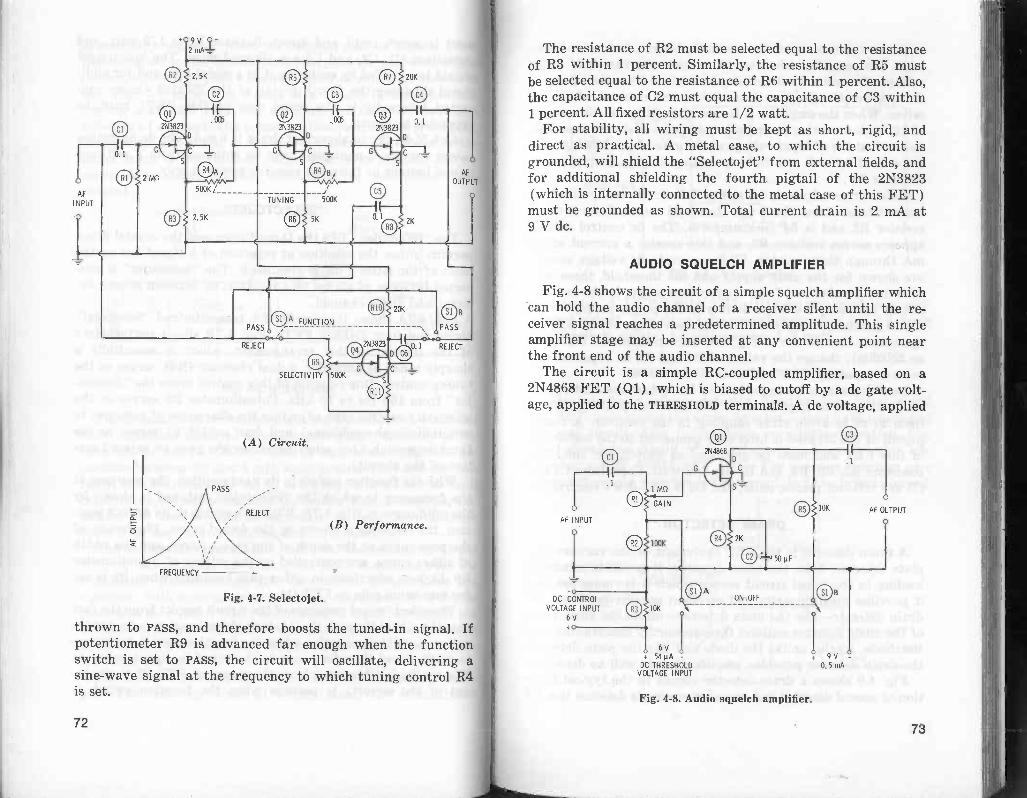
0
AF
INPUT
0
9 V 2-
2 rnA÷
0 2.5KI
R5
Ql 1(-.0E6
2N3823
C
o -REJECT
SELECTIVITY
(A) Circuit.
Fig. 4-7. Selectojet.
20K
00.1
D
2K
(B) Performance.
thrown to PASS, and therefore boosts the tuned -in signal. Ifpotentiometer R9 is advanced far enough when the functionswitch is set to PASS, the circuit will oscillate, delivering asine -wave signal at the frequency to which tuning control R4is set.
72
The resistance of R2 must be selected equal to the resistanceof R3 within 1 percent. Similarly, the resistance of R5 mustbe selected equal to the resistance of R6 within 1 percent. Also,the capacitance of C2 must equal the capacitance of C3 within1 percent. All fixed resistors are 1/2 watt.
For stability, all wiring must be kept as short, rigid, anddirect as practical. A metal case, to which the circuit isgrounded, will shield the "Selectojet" from external fields, andfor additional shielding the fourth pigtail of the 2N3823(which is internally connected to the metal case of this FET)must be grounded as shown. Total current drain is 2 mA at9 V dc.
AUDIO SQUELCH AMPLIFIER
Fig. 4-8 shows the circuit of a simple squelch amplifier whichCan hold the audio channel of a receiver silent until the re-ceiver signal reaches a predetermined amplitude. This singleamplifier stage may be inserted at any convenient point nearthe front end of the audio channel.
The circuit is a simple RC -coupled amplifier, based on a2N4868 FET (Q1), which is biased to cutoff by a dc gate volt-age, applied to the THRESHOLD terminals. A dc voltage, applied
AF INPUT
DC CONTROLVOLTAGE INPUT
6V
QlC3
6V+ 54 1.1A
DC THRESHOLDVOLTAGE INPUT
Fig. 4-8. Audio squelch amplifier.
73

to the DC CONTROL VOLTAGE terminals, bucks this bias and acti-vates the amplifier whenever it exceeds the threshold cutoffvoltage. The control voltage may be derived from the i-f ampli-fier (by rectification) or from the second detector of the re-ceiver. When the amplifier is in operation, it has a voltage gainof 10, with a maximum undistorted output of 1 volt rms. Thismeans that the of input voltage at the gate of the 2N4868 mustnot exceed 0.1 volt rms for any setting of gain -control poten-tiometer R1 .
Main current drain is 0.5 mA at 9 V dc. Virtually all of thecurrent taken from the 6 -volt threshold source flows throughresistor R2 and is 54 microamperes. The de control voltageappears across resistor R3, and this creates a current of 0.6mA through that resistor. While separate dc voltage sourcesare shown for the main supply and the threshold, these volt-ages may be obtained from appropriate points in the receivercircuit (as along a voltage divider in the power supply).
If a particular receiver circuit gives voltage of the polarityopposite to that shown in Fig. 4-8, use a p -channel FET (suchas 2N2608), change the values of R4 and R5 as required, andreverse capacitor C2.
Lead dress may be important in individual installations, soall leads must be kept as short and direct as practical. Routethem so as to avoid stray coupling in the receiver. A fourthpigtail of the 2N4868 is internally connected to the metal caseof this FET and must be grounded as shown, for shielding.Resistors R2, R3, R4, and R5 are 1/2 watt. Capacitors C1 andC3 are 100 -volt plastic units, and C2 is a 25-dcwv electrolytic.
DRAIN DETECTOR
A drain detector is the FET equivalent of the vacuum -tubeplate detector. Like the plate detector, it presents minimumloading to the tuned circuit across which it is connected, andit provides good linearity and excellent sensitivity. Thus, thedrain detector-like the plate detector-offers the advantagesof the diode detector without the noteworthy disadvantages ofthe diode. Again, unlike the diode and like the plate detector,the drain detector provides amplification as well as detection.
Fig. 4-9 shows a drain -detector circuit in the typical func-tion of second detector in a superhet or simple detector in a trf
74
HEP F0010
RF or I -FTRANSFORMER
RFC1
2 112 mH
0.001
0.47
Fig. 4-9. Drain detector.
10K
0.6 mA9V
/0.1
AF
OUTPUT
front end. A HEP F0010 FET (Q1) is employed in a self -biased circuit. The circuit draws approximately 0.6 mA fromthe 9 -volt de supply. All resistors are 1/2 watt.
INFINITE -IMPEDANCE DETECTOR
The infinite -impedance detector, like the plate detector andits FET counterpart the drain detector, offers light loading ofa tuned circuit. Also, it introduces very little distortion. Fig.4-10 shows the circuit of an infinite -impedance detector em-ploying a HEP F0015 FET (Q1). The common function of asuperhet second detector is illustrated, but the infinite-imped-
I -F TRANSFORMER
HEP F0015
6200
9V0.2 mA
cl
Fig. 4-10. Infinite -impedance detector.
AF OUTPUT
75

ance detector finds use in other receiver positions, as well asin instruments and control devices.
The source bias resistor (R2) is rf-bypassed by 470-pF ca-pacitor C2 which does not greatly disturb the audio -frequencycomponent. The gate bias of approximately 6 volts developedby FET current flowing through this resistor determines thehigh signal -handling capability of this detector.
The circuit draws approximately 0.2 mA from the 9 -volt desupply. All fixed resistors are 1/2 watt. The 25,000 -ohm gain -control potentiometer (R3) has an audio taper.
SIMPLE RF MIXER
Fig. 4-11 shows the circuit of a simple, untuned, RC -coupledrf mixer (converter). Employing a HEP F0015 FET (Q1),this circuit mixes the signal and local -oscillator components inits gate section, and delivers the resulting i-f signal to a capaci-tive output -voltage divider (C4-05). The mixer is useful atfrequencies from the standard broadcast band through theamateur 10 -meter band.
The circuit draws approximately 1 mA from the 9 -volt dcsupply. All resistors are 1/2 watt. The 0.1 -millihenry rf choke(RFC1) is a Miller 4642 unit, and the screwdriver -adjusted3-40 pF trimmer capacitor (C5) is a Miller MA -1 mica com-pression unit. The output of the mixer is low impedance, being
0/71.20 pF
OF SIGNAL INPUT
9 V, 1 mA-
00.01
RFC, 0.1 mH
HEP F0015
CS
3 - 40 pF
300 if
I -F SIGNAL
OSCILLATOR OUTPUTINPUT
76
Fig. 4-11. Simple rf mixer.
taken across the 300-pF capacitor (C4) of the voltage divider.All connecting leads must be kept as short as practical in thevoltage divider. Capacitor C4 must be a high-grade silveredmica unit.
CASCODE PRESELECTOR
Fig. 4-12 shows the circuit of a preselector employing twoHEP F0015 FETs (Q1, Q2) in a cascode arrangement. Thispreselector will provide a 20- to 25 -dB boost to signals. Con-tinuously variable tuning is afforded by the dual 50-pF vari-able capacitor, C1A-C1B. While the circuit is shown here toaccommodate plug-in coil combinations (Ll-L2 and L3 -L4)and is usually so arranged for use in amateur bands from 10to 80 meters, a coil switching turret also may be employed. Thetuning range for each coil set is preset by adjustment of theslug in L2 and L3, with C1A-C1B set to minimum capacitance.The inductance of the coils must be chosen for resonance with50 pF at the desired signal frequency (see "Conventional Crys-tal Oscillator" in Chapter 3). Low -impedance input and outputare provided by link -coupling coils L1 and L4.
The circuit draws approximately 2 mA from the 9 -volt desource. All resistors are 1/2 watt. All fixed capacitors must bemica or good -grade ceramic. Good shielding is essential in con-struction of the preselector.
RF
INPUT
(:)
4I r0
00.001
HEP F0015 HEP F0015 w.D 18
TUNING
--sner1600 0 33K
818200
To. ow
Fig. 4-12. Cascode preselector.
0+ 9 V, 2 mA
RECI 1 mH
if?0.001
C1 8I50
RF
OUTPUT
12
F.00
77

5
Transmitterand Transmitter -Accessory Circuits
The special features of the FET that recommend this tran-sistor for use in oscillators (see Chapter 3) also enable it toperform efficiently in low -powered transmitter circuits. Infact, many tube -type oscillator and rf amplifier circuits fortransmitters need no change other than voltage reduction ifthe tubes are replaced with suitable FETs. This means thatstandard coils, tuning capacitors, and chokes may be used, andalso that no loss results in capacitance -type interstage couplingin transmitters and exciters. Furthermore, the high input im-pedance of the FET tends to preserve the high Q of the trans-mitter tank circuit.
Low -powered circuits offering high overall efficiency andrelative simplicity are possible in this area with FETs. Thetransmitter circuits described in this chapter are of special in-terest to the radio experimenter, novice, and ham, but theywill also suggest applications to communications professionals.In addition to actual transmitters, some accessory devices foruse in transmitting stations are described. Additional devicesmay be found in Chapter 7.
Operation of transmitters is regulated by the Federal Com-munications Commission (FCC). Be sure you are complying
79

with their rules and procedures before you attempt to put asignal "on the air."
SINGLE -STAGE CRYSTAL -CONTROLLED TRANSMITTER
Fig. 5-1 shows the circuit of a simple crystal -controlled,oscillator -type cw transmitter with a low -impedance output.This single -stage unit, based on a 2N3823 FET, covers the ama-teur bands from 10 to 80 meters and is capable of 56 milliwattsde power input.
C.)2N3823
®
RF OUTPUT
KEY
0-5 DC 1+M I LL IAMMETER DC INPUT
Fig. 5-1. Single -stage 56-mW crystal -controlled transmitter.
The circuit is that of the basic drain -tuned crystal oscillator.The tuned tank circuit comprises .50-pF variable capacitor C2and tank coil Ll. Each plug-in "coil" consists of a tank coil(L1) and link -coupling coil (L2) as a unit (Millen low -pow-ered, single -ended 40,000 series, or equivalents) , and separateplug -ins are available for the 10-, 20-, 40-, and 80 -meter hambands. Special coils wound to suit individual demands willcover other frequencies. .
The low -impedance output may feed a coaxial antenna feederdirectly or may operate into a suitable antenna coupler. Inportable emergency applications, a whip antenna may be con-nected directly to the top of coil L1.
With the key depressed, the circuit is tuned, without antennaor other load, by adjusting C2 for drain -current dip, as indi-cated by 0-5 dc milliammeter Ml. The antenna then is con-nected, and any adjustments made to the antenna coupler (if
80
one is used) to "load" the drain current up to the highest valueat which the oscillator starts readily each time the key isclosed. Drain current is 1.40 mA at 6 V dc, 1.41 mA at 9 V dc,2.0 mA at 15 V dc, and 2.5 mA at 22.5 V dc. With an activecrystal, the oscillator can be made to act as a doubler, i.e., tankL1 -C2 may be tuned to twice the crystal frequency. The rf out-put will be lower, however, than in straight -through operation.
In addition to serving as a single -stage transmitter, this cir-cuit may also be used as the crystal oscillator in a multistagetransmitter. Either inductive or capacitive output couplingmay be used in the latter application.
All wiring must be kept as short and rigid as practical. Andthe fourth pigtail of the 2N3823 (being internally connected tothe metal case of this FET) must be grounded as shown. Re-sistors R1 and R2 are 1/2 watt; capacitors C1 and C3 are mica.
SINGLE -STAGE 0.8 -WATT CRYSTAL -CONTROLLEDTRANSMITTER
The U222 FET will provide a maximum of 1 watt rf outputat frequencies as high as 200 MHz. This capability makes theU222 especially attractive for transmitter use.
Fig. 5-2 shows the circuit of a single -stage crystal -controlledcw transmitter using the U222. This circuit is similar to theone described in the preceding section, except that the U222circuit employs shunt feed of the de supply through a 2.5-mH
TSXTAL
0U222
D
0-50 DC
MILLIAMMETERKEyC
=-165:1G
I.
001 /t.
22.5 V
I-
RF
OUTPUT
Fig. 5-2. Single -stage 0.8 -watt crystal -controlled transmitter.
81

rf choke (L3). This allows the bottom of the tank circuit, Li -C4, to be grounded. Plug-in coil sets (Ll-L2) permit the trans-mitter to be tuned to any frequency for which a crystal isavailable. Each plug-in set consists of a tank coil (Li) and link -coupling coil (L2) assembled as a unit. The Millen 40,000 seriesof low -powered single -ended coils provides sets for the 10-, 20-,40-, and 80 -meter ham bands. For nonham frequencies, otherL1 -L2 coils may be wound to suit individual demands.
The circuit is tuned, with the key depressed and with no an-tenna or other load, by adjusting C4 for drain -current dip, asindicated by 0-50 dc milliammeter M1. Then, the antenna isconnected and any adjustments made to the antenna coupler(if one is used) to "load" the drain current up to 35 mA mini-mum. At this point, the de power input is 0.8 watt. The low -impedance output may be connected directly to a coaxial an-tenna feeder or may operate into a suitable antenna coupler.
Like the preceding single -stage transmitter (Fig. 5-1), thisone may serve either as a complete cw transmitter or as theoscillator of a multistage transmitter.
Resistors R1 and R2 are 1/2 watt, and capacitors Cl, C2,and C3 are mica. All wiring must be short and rigid, for sta-bility. The gate electrode of the U222 is internally connectedto the metal case of this FET which accordingly must be keptout of contact with other components.
TWO -STAGE TRANSMITTER
Fig. 5-3 shows the circuit of a crystal -controlled oscillator -amplifier type of transmitter, employing single -ended stages.A 2N3823 FET is used in the oscillator (Q1) and a U222 FETin the rf amplifier (Q2) . The dc power input of the amplifieris 0.8 watt.
The oscillator is tuned by tank circuit Ll-C2. Here, Ll is aplug-in coil chosen to resonate with C2 at the crystal frequency.The amplifier is tuned by tank circuit L2 -C6, and here a plug-incoil set (L2 -L3) is used: L2 resonates with C6 at the crystalfrequency, and L3 is a link -coupling coil. For ham bands, theoscillator and amplifier coils both may be commercial low --powered units, such as the Millen 40,000 series of single -endedunits. For Ll, the main coil is used without the link winding.The low -impedance RF OUTPUT terminals of the transmitter can
82
Ql 2N3823
OSCILLATOR
Fig. 5-3. Two -stage transmitter.
feed a coaxial antenna feeder directly or can operate into asuitable coupler for a higher -impedance antenna.
A single 0-1 dc milliammeter (M1) is used for tune-up pur-poses. When meter switch Si is in its osc position, the meteris switched across 27 -ohm resistor R3, the scale is converted to0-3 mA, and the meter reads oscillator current; when Si is inits AMP position, the meter is switched across 1.3 -ohm shuntresistor R6, the scale is converted to 0-43 mA, and the meterreads amplifier current. (Both shunt resistors are stockvalues.) The transmitter is tuned to the crystal frequency, inthe conventional manner, by adjusting first the oscillator ca-pacitor (C2) and then the amplifier capacitor (C6) for drain-
current dip. Common drain -current values are 2.5 mA for theoscillator and 35 mA for the amplifier.
All wiring must be kept as short, direct, and rigid as prac-tical. Overall shielding, such as complete enclosure in a metalbox, is advantageous but not mandatory. However, the fourthPigtail of the 2N3823 (being internally connected to the metalcase of this FET) must be grounded as shown. The gate elec-trode of the U222 is internally connected to the metal case ofthat FET, so the U222 must be kept clear of all contact with
83

;r-
other components and wiring. All fixed resistors are 1/2 waand all fixed capacitors are mica.
PUSH-PULL FINAL AMPLIFIER
A push-pull final amplifier capable of approximately 1.6watts dc power input is shown in Fig. 5-4. This amplifier maybe driven by the two -stage circuit shown in Fig. 5-3 or by thecrystal oscillator shown in Fig. 5-2. Two U222 FETs are used.
The amplifier employs link -coupled input and output (low -impedance coupling coils L1 and L4). For ham bands, plug-incoils (such as the Millen 40,000 series, low -powered, center -tapped type) may be used both for the input (L1 -L2) and out-put (L3 -L4) tanks. Both tanks are tuned to the incomingfrequency.
15 pF
(Q1)U222
15 pF
0-103 DCMILLIAMMETER
Fig. 5-4. Push-pull final
22.5 V
_ 70 mA
amplifier.
CCF OUTPUT
.001
In many instances, the amplifier will self -oscillate and willneed to be neutralized. The 15-pF variable capacitors (C3,C4) are indicated for this purpose, but will not be needed inevery layout. The circuit should be tried first without them,noting if self -oscillation occurs at any setting of tuning capaci-tors C1A-C1B and C5A-05B. Neutralizing is accomplished inthe conventional manner.
84
All wiring must be kept short, direct, and rigid ; and careshould be taken to avoid contact between the FETs or betweenthem and other components, since the gate electrode is inter-nally connected to the metal case of the U222. Resistors R1 andR2 are 1 watt, and capacitors C2 and C6 are mica.
Current drain is approximately 70 mA at 22.5 volts, but maybe higher with individual FETs.
100 -MHz GROUNDED -GATE AMPLIFIER
The grounded -gate FET amplifier is the counterpart of thegrounded -grid tube amplifier. Neither of these amplifiers re-quires neutralization ; hence, both are usable at very high fre-quencies in circuits that are simpler than they otherwise mightbe. The grounded -gate (and grounded -grid) amplifier has theadditional advantage of somewhat higher output than that ofthe grounded source, grounded cathode, or grounded emitterunder similar operating conditions, since most of the excitationpower also appears in the amplifier output.
Fig. 5-5 shows the circuit of a grounded -gate rf amplifiersuitable for 100 -MHz use. Employing a U183 FET, this ampli-fier has 50 -ohm input and output (available through coaxialjacks J1 and J2, respectively).
In this arrangement, the input (source -to -gate) circuit istuned by means of tank L1 -C2, and the output (drain -to -gate)circuit by means of tank L2 -C3. Variable capacitors Cl and C5are used for coupling and impedance matching. Each of the
0 ® U183
RF
INPUT
8.7 pF
0-10 DCMILL !AMMETER
Fig. 5-5. 100 -MHz grounded -gate amplifier.
RF
OUTPUT
15v4.5 mA
85

variable capacitors (C1 to C5) has a maximum capacitance8.7 pF (E. F. Johnson 160-104 midget, or equivalent), aneach of the tank coils (L1, L2) is a slug -tuned 0.184-0.275 ittunit (Miller 40A227CBI, or equivalent). The coil slugs are sto tune the tanks to 100 MHz with C2 and C3 at half-capacitance.
Current drain is 4.5 mA at 15 V dc ; this corresponds to a dpower input of 67.5 mW. The rf input (driving) power is aproximately 4 mW.
All wiring must be kept as short, direct, and rigid as prac-tical ; and the fourth pigtail of the U183, being internally connetted to the metal case of this FET, must be grounded asshown. Fixed capacitor C4 must be silvered mica.
SINGLE -ENDED FREQUENCY MULTIPLIER
Fig. 5-6 shows the circuit of a single -ended frequencymultiplier stage. Although this circuit gives best efficiency asa frequency doubler, it may also be used as a tripler. Operatiois entirely conventional: the output tank (L1 -C4) simply ituned to twice or to three times the frequency of the rf inputas desired.
The circuit, which employs a single U222 FET, maydriven by either of the crystal oscillators described earlie(Figs. 5-1 and 5-2), but substantially higher output astripler will be obtained when the oscillator of Fig. 5-2 is useas the driver.
r001RI INPUT
86
RFC
0 U222
0-50 DCMILL (AMMETER
001
.001
22.5 V_ 35 mA
Fig. 5-6. Single -ended frequency multiplier.
RF OUTPUT
Inductance L1 is selected to resonate with capacitance C4at the desired multiple of the input -signal frequency. For theham bands, plug-in coils may be any of the commercial low -powered units, such as the Millen 40,000 series. Either capaci-tive output coupling may be used, as shown in Fig. 5-6, into ahigh -impedance load ; or low -impedance inductive couplingmay be obtained with the link coil supplied as part of the com-mercial plug-in coils (L1).
The dc power input is approximately 0.8 watt (35 mA at22.5 V dc). Drain -current dip, as indicated by 0-50 dc milli -ammeter Ml, indicates correct tuning of the multiplier.
All wiring must be kept short, direct, and rigid ; and sincethe gate electrode of the U222 is internally connected to themetal shell of this FET, the latter must be kept out of con-tact with other components and wiring. All resistors are 1/2watt, and all fixed capacitors are mica.
PUSH -PUSH DOUBLER
The push -push doubler, using two tubes or transistors, givesapproximately twice the rf power output of the single -endeddoubler. Fig. 5-7 shows the circuit of a push -push doubler em-ploying two U222 FETs.
Note that, in the conventional manner, the gates are con-nected in push-pull and the drains in parallel. Because of this
Ll
RF
INPUT
Fig. 5-7. Push -push doubler.
0-100 DCMILL [AMMETER
87

arrangement, a center -tapped input tank coil (L2) and single -ended output tank coil (L3) are required. (Both tanks are linkcoupled, the input through L1 and the output through L4.) Theinductance of L2 is selected to resonate with dual tuning capaci-tor C1A-C1B at the input frequency, and the inductance of L3to resonate with tuning capacitor C4 at twice the input fre-quency. Input- and output -coil sets may be low -powered com-mercial plug-in units, such as the Millen 40,000 series.
Tuning procedure is conventional: tune the input tank tothe input frequency by adjusting C1A-C1B for peak deflectionof milliammeter M1; then adjust the output tank for drain -current dip at twice the input frequency, as indicated by milli -ammeter M2. The dc power input is approximately 1.6 watt(70-mA drain current at 22.5 V dc).
All wiring must be as short, direct, and rigid as practical.Resistors R1 and R2 are 1 watt, and all fixed capacitors aremica. The U222s must be kept clear of contact with each otherand with wiring and other components, since the gate elec-trode is internally connected to the metal case of this FET.
FOUR -BAND EXCITER
Fig. 5-8 shows the circuit of a standard four -band exciter forham radio. This arrangement consists of a crystal oscillator(Q1) followed by three doublers (Q2, Q3, Q4), each stage con-taining a single U222 FET. The output (f1) of the oscillatoror that of the doublers (f2, f3, f4) is selected, as desired, bymeans of the single -pole, four -position rotary switch, S2. Allrf outputs are capacitance coupled (through C4, C9, C14, andC19, respectively). In a popular application of this type ofexciter, the crystal oscillator operates in the 80 -meter band,and the doublers in the 40-, 20-, and 10 -meter bands, respec-tively.
The various stages are tuned by means of separate tank ca-pacitors: C2 for the oscillator; C7, first doubler; C12, seconddoubler; and C17, third doubler. Each stage is tuned in theconventional manner, starting with the oscillator and progress-ing through the exciter, for drain -current dip. For economy inthis tuning, a single 0-1 de milliammeter (M1) is switched (bymeans of S1) across a shunt resistor (R3, R6, R9, R12) in anystage being adjusted. These resistances are low enough that
88
Fig. 5-8. Four -band exciter.
(JO
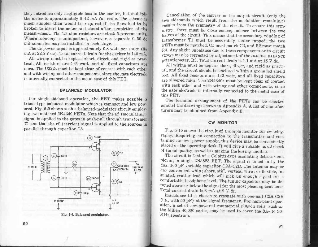
they introduce only negligible loss in the exciter, but multiplthe meter to approximately 0-42 mA full scale. The schememuch simpler than would be required if the lines had to bbroken to insert the meter and closed after completion of thmeasurement. The 1.3 -ohm resistors are stock 5 -percent units.Where economy is unimportant, however, a separate 0-50 demilliammeter may be installed in each stage.
The de power input is approximately 0.8 watt per stage (35mA at 22.5 V dc). Total current drain for the exciter is 140 mA.
All wiring must be kept as short, direct, and rigid as prac-tical. All resistors are 1/2 watt, and all fixed capacitors aremica. The U222s must be kept clear of contact with each otherand with wiring and other components, since the gate electrodeis internally connected to the metal case of this FET.
BALANCED MODULATOR
For single-sideband operation, the FET makes possible atriode -type balanced modulator which is compact and low pow-ered. Fig. 5-9 shows such a balanced -modulator circuit employ-ing two matched 2N4340 FETs. Note that the of (modulating)signal is applied to the gates in push-pull through transformerT1 and that the rf (carrier) signal is applied to the sources inparallel through capacitor C3.
AF INPUT
90
Ql2N4340
S
100 pF
0RF INPUT
I
15K
CARRIERTO
S I DEBANDBALANCE
FILTER
15K
15 V
11.1mA
Fig. 5-9. Balanced modulator.
Cancellation of the carrier in the output circuit (only thetwo sidebands which result from the modulation remaining)results from the symmetry of the circuit. To ensure this sym-metry, there must be close correspondence between the twohalves of the circuit. This means that the secondary winding oftransformer T1 must be accurately center tapped, the twoFETs must be matched, C1 must match C2, and R2 must matchR4. Any slight unbalance due to these components or to circuitstrays may be corrected by adjustment of the CARRIER BALANCEpotentiometer, R3. Total current drain is 1.1 mA at 15 V dc.
All wiring must be kept as short, direct, and rigid as practi-cal, and the circuit should be enclosed within a grounded shieldbox. All fixed resistors are 1/2 watt, and all fixed capacitorsare silvered mica. The 2N4340s must be kept clear of contactwith each other and with wiring and other components, sincethe gate electrode is internally connected to the metal case ofthis FET.
The terminal arrangement of the FETs can be checkedagainst the drawings shown in Appendix A. A list of manufac-turers may be obtained from Appendix B.
CW MONITOR
Fig. 5-10 shows the circuit of a simple monitor for cw teleg-raphy. Requiring no connection to the transmitter and con-taining its own power supply, this device may be convenientlyplaced on the operating desk. It will give a reliable aural checkof signal quality, as well as making the keying audible.
The circuit is that of a Colpitts-type oscillating detector em-ploying a single 2N3823 FET. The signal is tuned in by thedual 100-pF variable capacitor C2A-C2B. The antenna may beany convenient whip ; short, stiff, vertical wire ; or flexible, in-sulated, scatter lead which will pick up enough signal for acomfortable headphone level. The tuning capacitor may be de -tuned above or below the signal for the most pleasing beat tone.Total current drain is 3 mA at 9 V dc.
Inductance Ll is chosen to resonate with one-half C2A-C2B(i.e., with 50 pF) at the signal frequency. For ham -band oper-ation, a set of low -powered commercial plug-in coils, such asthe Millen 40,000 series, may be used to cover the 3.5- to 30 -MHz spectrum.
91

ANTENNA
Fig. 5-10. A cw monitor.
2000 0HEADPHONES
ON -OFF
The volume delivered by a pair of high -impedance magneticheadphones will be sufficient in most environments, especiallywith medium- and high -power transmitters. However, a tran-sistorized audio amplifier may be added to the monitor ifspeaker operation or louder headphone signals are desired.
All wiring must be kept as short, direct, and rigid as prac-tical, and the monitor circuit should be enclosed in a shield boxto which the circuit is grounded. For further shielding, thefourth pigtail of the 2N3823 (which is internally connected tothe metal case of this FET) must be grounded as shown. Re-sistor R1 is 1/2 watt, and capacitors C1, C3, and C4 are mica.The terminal arrangement for the FET is shown in Appen-dix A.
MODULATING THE FET TRANSMITTERS
The FET transmitters shown in this chapter are depictedfor cw telegraph operation. They may be amplitude modulatedfor telephony, however, by short-circuiting the telegraph keyand connecting a suitable af speech amplifier/modulator unitin series with the transmitter dc supply, as shown in Fig. 5-11.
The only requirements are that the af power output of themodulator must be at least twice the de drain power input ofthe transmitter, and that the impedance (Za) of the modulatoroutput transformer, T., match the impedance of the transmit -
92
MICROPHONE
SPEECHAMPLIFIER/ MODULATOR
IIIIIIAMPLIFIER / MODULATOR
DC SUPPLY
TO DC INPUT TERMINAL OF FETTRANSMITTER
_ TRANSMITTER
DC SUPPLY
Fig. 5-11. Amplitude -modulation arrangement.
ter. Table 5-1 shows the values of impedance (for each of theapplicable transmitters in this chapter) which transformer T.in the modulator must match. It also shows the af output powerneeded to modulate each of the transmitters 100 percent. Theprimary impedance (Zm) of the transformer matches the im-pedance of the transistor (s) in the modulator.
Table 5-1. A -M Modulator Data
TransmitterCircuit
TransmitterDc Voltage
Af Power(Milliwatts)
Transmitter Im-pedance (Ohms)
Fig. 5-1* 6.0 16.8 42909.0 25.4 6360
15.0 60.0 750022.5 56.2 9000
Fig. 5-2* 22.5 1600 645
Fig. 5-3 22.5 1600 645
Fig. 5-4 22.5 3200 32.2
Fig. 5-5 15.0 135 3300
Fig. 5-6 22.5 1600 645
Fig. 5-7 22.5 3200 32.2_ ... . .
u a e oscillators are prohibited in some services.
Note that the modulation must be applied to the final rfstage in the transmitter circuit given in Fig. 5-3.
93

SINGLE -CONTROL ("TNT") TRANSMITTER
Fig. 5-12 shows the circuit of a cw transmitter. This is avariation of the tuned -plate, tuned -grid (TPTG) oscillatorwhich uses tuning only in the output circuit. An untuned coilis used in the input circuit. This accounts for the descriptiveterm TNT ("tuned, nontuned").
In the arrangement shown here, the drain circuit is tunedby means of 50-pF variable capacitor C2 and a plug-in coil.Each plug-in coil set (Millen 43,000 series, or equivalent) con-sists of an untapped main coil (L4) and end link (L5) . Threesets provide coverage of the 3.5-, 7-, and 14 -MHz amateurbands. Corresponding untuned gate coils (L1, L2, and L3) forthese bands are selected by means of single -pole, three -positionswitch S1. The gate coils are preadjusted by means of theirscrewdriver -operated tuning slugs. (L1, 3.5 -MHz band, MillerNo. 40A475CBI. L2, 7 -MHz band, Miller No. 40A155CBI. L3,14 -MHz band, Miller No. 40A336CBI.)
The U222 FET (Q1) draws 35 mA at 22.5 volts dc, a dc in-put corresponding approximately to 0.8 watt. Lower dc volt-ages will produce correspondingly lower power input. A 0- to50 -dc milliammeter plugged into jack J2 allows drain currentto be read at intervals, or it can be monitored continuously.
In operation, the transmitter may be tuned throughout eachband simply by adjusting variable capacitor C2. There is suffi-cient distributed capacitance and circuit capacitance across thegate coil (L1, L2, L3) in most layouts that this coil, in true
BANDSWITCH
egKEY JACK
47K
c2 150 pF
TUNING
002[
RFC2 a 2.5 mH
?r.&+
DC POWER INPUT
?- (22.5 VI
L5
RF
OUTPUT
Fig. 5-12. Single -control ("TNT") transmitter.
94
MILLIAMMETERJACK
TNT fashion, needs no separate tuning. However, the trans-mitter output will be maximum around the one frequency atwhich the gate coil tends to self -resonate, and will fall off some-what at higher and lower frequencies. The optimum gate -coilinductance that will give best output throughout the band maybe selected by adjusting the gate -coil slug, varying capacitorC2, and noting the relative output as indicated by an rf vtvmconnected to the RF OUTPUT terminals, or by a 2 -volt pilot lamp(with a one -turn pickup coil) coupled to tank coil L4. In mostinstances, the gate coil will be adjusted for peak output at thecenter of the band. When maximum transmitter efficiency isdesired at some extreme frequency in any band, the appro-priate gate coil may be retrimmed for maximum output at thatfrequency.
The gate coils must be mounted at right angles to each otherand separated as widely as practical, to prevent power absorp-tion by the unused two. For maximum isolation, L1, L2, andL3 may be enclosed in separate shield cans.
Closed-circuit jacks are used both for the key (J1) and drainmilliammeter (J2). This allows the circuit to restore itselfautomatically when the key or meter is removed.
To prevent parasitic oscillation, all leads must be as short,rigid, and direct as practical. The U222 must be mounted clearof wiring, chassis, and all other components, since the gateelectrode is internally connected to the metal case of this FET.Resistor R1 is 2 watts, and capacitors C1 and C3 are mica.Selector switch S1 must be ceramic insulated.
The TNT circuit may be used as a doubler (3.5 to 7 MHz,and 7 to 14 MHz) if a driving signal is fed into the gate coiland the drain tank is tuned to twice the driving frequency.
PHONE MONITOR
A tuned diode detector with headphones is often used tomonitor radiophone transmissions. The semiconductor diodehas the advantage in this application that, at least for largesignals, its response is linear, so that it gives a faithful checkof the monitored signal. But its output is relatively low, so thatthe headphone signal cannot compete with room noise.
The solution is to use a headphone amplifier following thedetector. Fig. 5-13 shows an arrangement of this sort. The
95
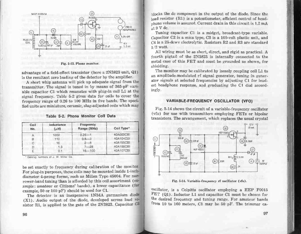
WHIP ANTENNA
PLUG-INCOIL
2N3823
Fig. 5-13. Phone monitor.
2000 C
HEADPHONES
ON -OFF
9V25 uF - 1.2 mA
advantage of a field-effect transistor (here a 2N3823 unit, Q1)is the resultant zero loading of the detector by the amplifier.
A short whip antenna will pick up adequate signal from thetransmitter. The signal is tuned in by means of 365-pF vari-able capacitor C1 which resonates with plug-in coil L1 at thesignal frequency. Table 5-2 gives data for coils to cover thefrequency range of 0.26 to 100 MHz in five bands. The speci-fied units are miniature, ceramic, slug -adjusted coils which may
Table 5-2. Phone Monitor Coil Data
CoilNo.
InductanceGAO
FrequencyRange (MHz) Coil Type*
A 1000 0.26-1 40A000CBI
B 110 0.8-3 40A104CBI
C 16 2-8 40A155CBI
D 1.3 7-28 40A156CB1
E 0.1 16-100 40A107CBI
Catalog numbers of J. W. Miller Co
be set exactly to frequency during calibration of the monitorFor plug-in purposes, these coils may be mounted inside 1 -inchdiameter 4 -prong forms, such as Millen Type 45004. For narower -band tuning than is afforded by this coil assortment (ex-ample: amateur or Citizens' bands), a lower capacitance (forexample, 50 or 100 pF) should be used for C1.
The detector is an inexpensive 1N34A germanium diod(X1). Audio output of the diode, developed across loadsistor R1, is applied to the gate of the 2N3823. Capacitor
96
blocks the de component in the output of the diode. Since theload resistor (R1) is a potentiometer, efficient control of head-phone volume is assured. Current drain in this circuit is 1.2 mAat 9 V dc.
Tuning capacitor C1 is a midget, broadcast -type variable.Capacitor C2 is a mica type, C3 is a 100 -volt plastic unit, andC4 is a 25-dcwv electrolytic. Resistors R2 and R3 are standard1/2 watt.
All wiring must be as short, direct, and rigid as practical. Afourth pigtail of the 2N3823 is internally connected to themetal case of this FET and must be grounded as shown, forshielding.
The monitor may be calibrated by loosely coupling coil L1 toan amplitude -modulated rf signal generator, tuning in gener-ator signals at selected frequencies by adjusting C1 for loud-est headphone response, and graduating the Cl dial accord-ingly.
VARIABLE -FREQUENCY OSCILLATOR (VFO)
Fig. 5-14 shows the circuit of a variable -frequency oscillator(vfo) for use with transmitters employing FETs or bipolartransistors. The arrangement, which replaces the usual crystal
+ 12V15mA /
TUNING
i.=.-
(DT
22 pF
Ql
HEP F0015
Of 100KRFC1 Z2.5 mH
01 1K
10068
Fig. 5-14. Variable -frequency rf oscillator (vfo).
1E--pF47
11 RF
OUTPUT
oscillator, is a Colpitts oscillator employing a HEP F0015FET (Q1). Inductor Ll and capacitor Cl must be chosen forthe desired frequency and tuning range. For amateur bandsfrom 10 to 160 meters, Cl may be 50 pF. The trimmer ca -
97

pacitor, C2, may be 15 pF and, together with the adjustmentof the slug in coil Ll, will set the upper -frequency limit of thetuning range.
Capacitances C4 and C5 are in the ratio of 10 to 1, and thiswill usually be satisfactory for good oscillation. However, anindividual FET may require some experimentation with thisratio for vigorous oscillation and maximum rf output. Diode
rectifies rf energy to provide a negative bias for the gate.The rf output is low impedance.
Fixed capacitors C3, C4, C5, C6, and C7 should be micaunits. For stability, all resistors should be 1 watt. The circuitdraws approximately 15 mA from the 12 -volt dc supply, whichshould be fully regulated. Solid construction and good shield-ing are imperative in the construction of the vfo.
BUFFER FOR VFO
In some installations, the vfo described in the preceding sec-tion may require isolation from the next transmitter stageinto which it operates. A buffer stage, which is useful for thispurpose and which will also boost the vfo output, is shown inFig. 5-15. This buffer employs a single 40820 MOSFET (Q1).This MOSFET is equipped with internal protective diodes (forsimplicity, not shown in the MOSFET symbol here) which au-tomatically prevent the gate from being damaged by carelesshandling of the MOSFET.
The circuit is an untuned RC -coupled rf amplifier with low -impedance output taken from across the 470 -ohm source re-
VFOINPUT
Fig. 5-15. Buffer for vfo.
98
RF
OUTPUT
sistor, R3, and it is useful in all amateur bands from 10 to 160meters. For stability, the resistors should be 1 watt, and thecapacitors should be mica or good -grade ceramic.
The buffer draws approximately 20 mA from the 12 -volt dcsupply. Solid construction and good shielding are imperativein the construction of the device.
99

6
Control Circuits
The sensitivity of the field-effect transistor to low signallevels and to small changes in level, together with its negligi-ble loading of timing circuits, signal circuits, and actuatingdevices, suits it to a variety of electronic control circuitrywhere special provision often must be made for the bipolartransistor. Usually, a simple FET circuit in a control systemoffers straightforwardness and economy not so easily obtainedwith either tubes or bipolar transistors.
In solid-state control circuits, the FET allows some compo-nents, such as high -resistance photocells and capacitive trans-ducers, to be operated with greater efficiency and conveniencethan is possible in such circuits containing bipolar transistors.
This chapter describes several basic control circuits that areintrinsically useful. Methods of operating relays from a varietyof signals-direct current, radio frequencies, audio frequen-cies, and illumination levels-are shown. Perhaps these canalso serve to generate ideas for other uses.
DC RELAY
Fig. 6-1 shows the circuit of an amplifier -type dc relay basedon a single 2N3819 FET. This circuit has an input resistanceof 10 megohms due entirely to resistor R1, so it draws only0.15 microampere from the dc control -signal source.
101

DC INPUT 00-1.5 V
BALANCE
06V
Fig. 6-1. A de relay.
TO
CONTROLLED
CIRCUIT
The 1000 -ohm, 1-mA dc relay (Sigma 5F, or equivalent) isconnected in a resistance -bridge circuit whose four arms areresistor R2, the internal drain -to -source resistance of the FET,and the two halves of potentiometer R3. With the DC INPUTterminals open, R3 is set to balance the static FET currentout of the relay (at balance, the relay opens firmly), and thebridge should remain balanced indefinitely without furtherattention.
Subsequent application of a dc input signal of 1.5 volts willunbalance the bridge by changing the FET drain -to -source re-sistance ; this will cause approximately 1.2 mA to flow throughthe relay, closing the latter. Up to 20 megohms may be usedat R1, thereby decreasing the drain on the signal source to aslittle as 0.075 microampere.
All fixed resistors are 1/2 watt. Maximum current drainfrom the 6 -volt dc supply (M1) is 10 mA. The 2N3819 isplastic -encapsulated FET which, because of this constructiondemands none of the installation precautions occasioned bmetal -cased units. The plastic housing will withstand solder-ing temperatures.
AC RF RELAY
The dc relay described in the preceding section may be actated by an ac or rf control signal if a diode rectifier is opeated ahead of the circuit, as shown in Fig. 6-2.
102
A shunt -diode rectifier circuit is used (C1 -R1 -X1) . The mainadvantage of the shunt diode is isolation from any dc compo-nent present in the signal source. In this arrangement, capaci-tor C1 is charged to the peak value of the ac signal (less thesmall forward voltage drop in the diode) on positive half -cycles of signal voltage, and this peak dc voltage (across 10-megohm load resistor R1) is presented to the gate of the FET.The diode must be polarized as shown for the de voltage at thegate to be negative. A silicon diode (1N3605) is required towork into the high load resistance, R1; the back resistance ofgermanium diodes is too low to support rectification with sucha high value of load. Resistor R2 and capacitor C2 form a filterto remove any signal -voltage fluctuations from the diode dcoutput.
AC RF INPUT0-0.71 V rms
Fig. 6-2. An ac rf relay.
TO
CONTROLLED
CIRCUIT
The 1000 -ohm, 1-mA dc relay (Sigma 5F, or equivalent) isconnected in a resistance -bridge circuit whose four arms areR3, the internal drain -to -source resistance of the FET(2N3819), and the two halves of potentiometer R4. With theAC -INPUT terminals open, R4 is set to balance the static FETcurrent out of the relay (at the balance point, the relay opensfirmly), and the bridge should then remain balanced indefi-nitely without further attention.
Subsequent application of an ac or rf input signal of 0.71volt rms will unbalance the bridge by changing the FET drain -to -source resistance, and this will cause approximately 1.2 mAto flow through the relay, closing the latter.
103
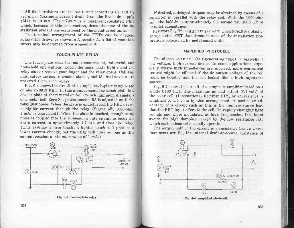
All fixed resistors are 1/2 watt, and capacitors Cl and C2are mica. Maximum current drain from the 6 -volt dc supply(M1) is 10 mA. The 2N3819 is a plastic -encapsulated FETwhich, because of this construction, demands none of the in-stallation precautions occasioned by the metal -cased units.
The terminal arrangement of the FETs can be checkedagainst the drawings shown in Appendix A. A list of manufac-turers may be obtained from Appendix B.
TOUCH -PLATE RELAY
The touch -plate relay has many commercial, industrial, andhousehold applications. Touch the metal plate lightly and therelay closes ; remove your finger and the relay opens. Call sig-nals, safety devices, intrusion alarms, and kindred devices areoperated from such relays.
Fig. 6-3 shows the circuit of a simple touch -plate relay basedon one 2N3819 FET. In this arrangement, the touch plate is adisc or plate of sheet metal or foil (2 -inch minimum diameter)or a metal ball. Zero Set potentiometer R3 is adjusted until therelay just opens. When the plate is undisturbed, the FET drawsnegligible current through the relay (Sigma 5F, 1000 -ohm,1-mA, or equivalent) . When the plate is touched, enough straynoise is coupled into the 10-megohm gate circuit to boost thedrain current to approximately 1.7 mA and close the relay.(This assumes a firm touch; a lighter touch will produce alower current change, but the relay will close as long as thiscurrent reaches a minimum value of 1 mA.)
METAL PLATE
1K W.W.
0 ON -OFFII
9 V ®
Fig. 6-3. Touch -plate relay.
104
TO
CONTROLLED
CIRCUIT
0
If desired, a delayed dropout may be obtained by means of acapacitor in parallel with the relay coil. With the 1000 -ohmcoil, the hold -in is approximately 0.8 second per 1000 ktF ofparallel capacitance.
Resistors R1, R2, and R4 are 1/2 watt. The 2N3819 is a plastic -encapsulated FET that demands none of the installation pre-cautions occasioned by metal -cased units.
AMPLIFIED PHOTOCELL
The silicon solar cell (self -generating type) is basically alow -voltage, high -current device. In some applications, espe-cially where high impedances are involved, more convenientcontrol might be effected if the dc output voltage of the cellcould be boosted and the cell looked like a high -impedancesource.
Fig. 6-4 shows the circuit of a simple dc amplifier based on asingle U183 FET. The maximum no-load output (0.4 volt) ofthe solar cell (International Rectifier S1M, or equivalent) isamplified to 1.6 volts by this arrangement. A particular ad-vantage of a circuit such as this is the high -resistance loadthat the FET input offers to the cell. On rapidly changing lightsignals and those modulated at high frequencies, this inputavoids the high damping caused by the low resistance intowhich such silicon cells usually operate.
The output half of the circuit is a resistance bridge whosefour arms are R1, the internal drain -to -source resistance of
22.5 V
Fig. 6-4. Amplified photocell.
RI
DC
OUTPUT
105

the FET, and the two halves of potentiometer R2. With thesolar cell completely darkened, R2 is set to balance the staticvoltage from the DC OUTPUT terminals (a dc vtvm temporarilyconnected to the output terminals will serve as a balance indi-cator). At the balance point, the indicator will read zero, andthe bridge should then remain balanced indefinitely withoutfurther attention.
Subsequent illumination of the cell will unbalance the bridgebecause the dc output voltage of the cell changes the drain -to -source resistance of the FET. This will cause 1.6 volts to ap-pear at the DC OUTPUT terminals. (This level of output voltagewill maintain itself across a 20,000 -ohm load.)
Wiring is uncritical. Resistor R1 is 1/2 watt, and poten-tiometer R2 is 1 watt. The fourth pigtail of the U183 is inter-nally connected to the metal case of this FET and should begrounded as shown. Total current drawn from the 22.5 -voltsource (M1) is 24 mA.
TIMER
Resistance-capacitance-controlled timers have been builtwith vacuum tubes, thyratron tubes, bipolar transistors of alltypes, and with no tubes or other active devices whatever. Thebipolar -transistor circuits, while offering the advantage ofcompactness, small size, light weight, freedom from the powerline, and zero heat generation, have been troublesome to de-sign because the low -impedance transistors load the re timingcircuit and impose undesirable limitations on it. The high in-put impedance of the field-effect transistor, however, allowsvacuum -tube performance to be attained in solid-state elec-tronic timers.
Fig. 6-5 shows the circuit of a timer employing a singleU183 FET. This is essentially a bridge -balanced dc amplifier,with a relay in its output circuit, which receives its driving sig-nal from a charged capacitor discharging through an adjust-able resistor. It provides a hold -in of the relay that ranges from1 second to 80 seconds, as selected by adjustment of theresistance.
The timing interval is determined by the number of secontaken by 100-p,F capacitor C1, after being full charged, to discharge through rheostat R1 to 0.4 of its charged voltage. Thi
106
capacitor is charged by momentarily depressing push-buttonswitch Si. This connects C1 to a 1.5 -volt tap on resistor R2.When released, the push-button blade returns to its normal po-sition against the upper contact, and this connects the chargedcapacitor to rheostat R1 and the gate of the FET.
ci
10 mA
Fig. 6-5. Timer.
TO
CONTROLLED
CIRCUIT
The 1000 -ohm, 1-mA dc relay (Sigma 5F, or equivalent) isconnected in a resistance bridge whose four arms are R3, theinternal drain -to -source resistance of the FET, and the twohalves of potentiometer R4. With capacitor Cl completely dis-charged, R4 is set to balance the static FET current out of therelay (at balance, the relay opens firmly), and the bridge thenshould remain balanced indefinitely without further attention.
To use the timer, depress Sl, charging capacitor Cl. Thenrelease this switch, whereupon the relay will pick up immedi-ately, since the negative voltage presented to the FET gate bythe charged capacitor unbalances the bridge, causing currentthrough the relay. The relay will hold in until the capacitorhas discharged sufficiently (through rheostat R1) to reducethe gate voltage to 0.4 of its value at full charge of the capaci-tor. This time interval depends on the resistance setting of R1,and the rheostat accordingly may be calibrated to read di-rectly in seconds. This may be done with a stopwatch, or thetime (t in seconds) may be calculated approximately from theresistance setting (R1 in ohms), the capacitance (C1 in
107

farads), and a multiplier (0.8 for the relay specified here).Thus :
t = 0.0001(0.8) R1 = 0.00008R1 seconds
With a 1-megohm volume control having an audio taper for R1,time intervals from 1 to 80 seconds may be read on a single dialscale.
Various combinations of capacitance and variable resistanceother than the 100 p,F and 1 megohm indicated in Fig. 6-5 maybe used. In any instance, the electrolytic capacitor used for thepurpose should be new and have a good power factor. Forclose reading or for coverage of narrow bands, severalswitched -in rheostats may be used against a single capacitor.
Resistor R3 is 1/2 watt; R2 and R4 may be wirewound rheo-stats with slotted shafts for screwdriver adjustment. Alterna-tively, R2 may be a stick -type resistor with slider. Electro-lytic capacitor C1 is rated at 25 dcwv. The fourth pigtail of theU183 is internally connected to the metal case of this FET andshould be grounded as shown.
FET AS VOLTAGE -VARIABLE RESISTOR
Since at any value of drain -to -source dc voltage, the draincurrent is a function of the applied gate -to -source bias voltage,
10
U222
-ADC
CONTROLVOLTAGE
C
RES ISTORTERMINALS
D-
(A) Circuit.
8
,560
0
6 4
2
0
103
VDS15 Vdc1 mA
75 mA
10 mA
8 mA
21
mA)
26 mA
30 mA
1K
RESISTANCE (OHMS)
(B) Performance.Fig. 6-6. FET as voltage -variable resistor.
108
OK 20K
the instantaneous value of internal drain -to -source resistancedepends on the dc gate bias. This provides a convenient meansof varying resistance with a variable voltage; and since thecorrectly polarized gate bias results in virtually zero gate cur-rent, the process is essentially a voltage -controlled one.
Fig. 6-6A shows the simple setup of a U222 (high -current)FET as a voltage -controlled resistor. Here, the control voltage(as gate bias) is applied to terminals A and B. Looking intoterminals C and D, one sees a resistor varied by the voltage onA and B. In use, this "resistor" is connected in series with ade supply and load device, the supply being polarized so thatC is positive and D negative. Some devices in which a voltage -variable resistor is advantageous are voltage regulators, signaltranslators, voltage -tuned frequency -sensitive RC networks,voltage -tuned audio oscillators, remote -control devices, tem-perature transducers, and remote volume controls.
Fig. 6-6B shows performance of the resistor when the volt-age between C and D is 15 volts. Note that the resistancevaries from 500 ohms (when the control voltage is zero) to15,000 ohms (when the control voltage is -8 volts). Other re-sistance ranges are obtained when the C -D voltage is somevalue other than 15 volts. The power -handling capability of thevariable FET resistor corresponds to the rated power dissipa-tion of the FET. (The manufacturer gives 300 mW as the ab-solute maximum device dissipation for the U222 at 25°C free -air temperature.) Note that the corresponding drain -currentvalues are given along the curve in Fig. 6-6B.
When using any FET as a voltage -variable resistor, keepwell within the maximum safe drain -to -source voltage, drain -current, and device -dissipation ratings supplied by the FETmanufacturer. The "resistor" may be calibrated by successivelyapplying the various intended values of bias voltage and notingthe corresponding drain current. The resistance is calculated ateach point as VD/ID, where VD is the instantaneous drain -to -source voltage (in volts) and ID is the corresponding draincurrent (in amperes).
CONSTANT -CURRENT SOURCE
The pentode -like drain-voltage/drain-current characteristiccurves of the FET suit this component for use as a constant -
109

current adapter. Fig. 6-7 shows the circuit of such an adapteremploying a 2N4859 FET.
The adapter is connected in series with an external dc powersupply and the device operated from the supply, with the sup-ply polarized correctly to make terminal A of the adapter posi-tive and B negative. Potentiometer R1 then is set for the de-sired load current, as indicated by 0-50 de milliammeter M2.(With the 2N4859, this may be any value between 1 and 40mA.) That current level then will be maintained automaticallywithin 6 percent, even if the voltage of the external supplyvaries between 3 and 20 volts.
22.5 V
45 µA
0 \ ON -OFF
2N4859
D0-50 DC
M I LLI AMMETER
Fig. 6-7. Constant -current source.
A.+ADAPTER
TERMINALS
Current drain from the 22.5 -volt gate bias supply, Ml, is 45microamperes, which is due entirely to current through the 0.5-megohm potentiometer, R1. Resistor R2 is 1/2 watt.
SENSITIVE AC AF RELAY
Using two FETs (Q1, Q2) and one silicon bipolar transistor(Q3), the circuit given in Fig. 6-8 closes a 1 -milliampere, 5 -volt de relay (K1) in response to an input signal of only 0.1volt rms (at approximately 0.1 microampere), when gain con-trol R4 is set to maximum. Good response is obtained through-out the spectrum from 50 Hz to 50 kHz.
The input signal is amplified by a two -stage RC -coupled sec-tion based on two FETs: 2N4868 (Q1) and 2N4340 (Q2). Theamplified signal then is rectified by the 1N34A diodes (Xl,X2), and the resultant direct current is amplified by a 2N2712plastic -encapsulated silicon bipolar transistor (Q3) and ap-
110
plied to the 1-mA, 5000 -ohm dc relay (K1, Sigma 5F, orequivalent).
With zero input signal, the 2N2712 draws virtually no cur-rent, and the total circuit drain is 1.8 mA at 9 V dc. With a0.1 -volt input signal (R4 set for maximum gain), the circuitdrain rises to 2.8 mA.
All fixed resistors are 1/2 watt. Capacitors Cl, C3, C5, andC6 are 100 -volt plastic units, and C2 and C4 are 25-dcwvelectrolytics.
0AC INPUT
(0. IV rms MAX)0
Fig. 6-8. Sensitive ac of relay.
f-10CONTROLLED
CIRCUIT
For stability, all wiring must be kept as short, direct, andrigid as practical, and the entire unit should be enclosed in agrounded shield box if interfering fields are present. A fourthpigtail of the 2N4868 is internally connected to the metal shellof this FET and must be grounded as shown, for shielding. Inthe 2N4340, the gate electrode is internally connected to themetal case, so this FET must be mounted clear of chassis, wir-ing, and other components. Signal input leads to the AC INPUTterminals should be shielded.
SOUND -OPERATED RELAY
Fig. 6-9 shows the circuit of a sound -operated relay based ontwo 2N4868 FETs (Q1, Q2) and one U183 FET (Q3). Withthis arrangement, a microphone output signal of 1.8 millivoltsrms (-52.5 dB) will close the 1-mA, 1000 -ohm dc relay (K1)when sensitivity control R4 is set to maximum.
111

The first two stages form a high -gain RC -coupled amplifier,the output of which is rectified by the 1N3605 silicon diode,X1. The resultant dc output voltage of the diode, developedacross load resistor R7, is applied to the gate of the U183 FE T(Q3) through the resistance -capacitance filter R8 -C6. TheU183 acts as a dc amplifier which drives a 1-mA, 1000 -ohm derelay (Sigma 5F, or equivalent). Current drain is 12 mA at9 V dc.
CRYSTALOR CERAMICMICROPHONE
Fig. 6-9. Sound -operated relay.
0TO
CONTROLLEDCIRCUIT
0
Initial adjustment of the circuit consists of balancing thestatic drain current of the U183 out of the relay :
1. Short-circuit the microphone terminals.2. Set potentiometer R4 for maximum sensitivity.3. Adjust potentiometer R10 until relay K1 opens.
(This adjustment may be made very precisely if a dc vtvm is
connected across the relay coil and R10 is adjusted for zerodeflection of the meter.)
All fixed resistors are 1/2 watt. Potentiometer R10 is wire -wound. Capacitors Cl, C3, C5, and C6 are 100 -volt plasticunits, and C2 and C4 are 25-dcwv electrolytics. The high -impedance input of the first stage will accommodate a crystalor ceramic microphone directly ; for a dynamic microphone, use
an appropriate input transformer.
112
For stability and minimum stray signal pickup, all wiringmust be as short, direct, and rigid as practical. For completeshielding in electrically noisy locations, the entire unit mustbe enclosed in a grounded metal box. In each of the FETs, afourth pigtail is internally connected to the metal case andmust be grounded as shown, for shielding.
MODULATED -LIGHT DETECTOR/AMPLIFIER
The S1M silicon solar cell is a good detector of modulatedlight (either chopped or smoothly modulated), and its af out-put is easily amplified. Fig. 6-10 shows a circuit composed of aS1M cell (X1) and a two -stage RC -coupled af amplifier em-ploying two 2N2608 FETs (Q1, Q2).
The sensitivity of this circuit is such that 5 foot-candles oflight modulated or chopped at a 1000 -Hz rate will produce 1volt rms (no load) at the AF OUTPUT terminals when poten-tiometer R4 is set for maximum gain. Current drain is 5 mAat 9 V dc.
The detector/amplifier has many uses, such as light -beamcommunication, alarm signaling, intrusion alarm service,sound -on -film pickup, and optoelectronic control. The virtuallyzero loading of the silicon cell by the amplifier results in maxi-mum efficiency of the S1M, while the amplifier produces a use-ful output -signal amplitude for direct application or furtheramplification.
0SILICONCELL
S1M
BLACK
RED
1M4
- 9V +
I.5 mA
070N -OFF
0 3.3K CI)
2N2608
330
3.3K
Fig. 6-10. Modulated light detector/amplifier.
50 uF
AF
OUTPUT
113

All fixed resistors are 1/2 watt. Capacitors C1 and C3 are100 -volt plastic units, and C2 is a 25-dcwv electrolytic. In the2N2608s, the gate electrode is internally connected to the metalcase of the FET, so each of these units must be mounted clearof other components, chassis, and wiring. All wiring must beas short, rigid, and direct as practical.
PHASE SHIFTER
The circuit given in Fig. 6-11, combining a triode phase in-verter and an adjustable RC circuit, provides continuouslyvariable phase shift from 0 to 180 degrees while leaving thesignal amplitude virtually untouched.
Oi/9V
ON -OFF =
INPUT500K
PHASE SHIFT
CLOSELY MATCHED
Fig. 6-11. Phase shifter.
OUTPUT
This arrangement, based on one 2N2608 FET (Q1), hasequal fixed resistances (R2 and R3, matched within 1 per-cent) in both drain and source legs. When rheostat R4 is set toone end of its range, the output is taken from the source of Q1and is in the same phase as the input signal (Q1 is then actingas a source follower) ; therefore, there is zero phase shift be-tween output and input. But when R4 is set to the opposite endof its range, the output is taken from the drain of Q1 and is ofopposite phase from the input (Q1 then is acting as a conven-tional triode amplifier) ; therefore, there is then 180 degreesphase shift between output and input. At intermediate settingsof R4, the various phase angles between 0 and 180 degrees are
114
obtained. Two identical stages may be cascaded for 0 to 360degrees phase shift.
The circuit provides good, full -range operation between 150liz and 5 kHz. Below 150 Hz and above 5 kHz, inherent phaseshifts in the circuit and components restrict the range to limitssomewhat higher than zero degrees on one end and somewhatlower than 180 degrees on the other. However, some improve-ment may be obtained by careful attention to lead dress andshortness of leads, and to minimization of stray capacitances.
For undistorted operation, the maximum input -signal am-plitude is 2 volts rms. With potentiometer R1 set for maximumgain, the corresponding output -signal amplitude is 0.75 voltrms. Current drain is 1 mA at 9 V dc.
Resistors R2 and R3 are 1 watt and are of the 1 -percentnoninductive, wirewound type. Capacitor Cl is silvered mica.
All wiring must be as short, rigid, and direct as practicaland kept well away from the metal chassis if one is used. Theinput and output circuits must be kept well separated. In the2N2608, the gate electrode is internally connected to the metalcase, so this FET must be mounted clear of other components,wiring, and chassis.
The dial of the phase -shift control, R4, may be calibrated indegrees by means of Lissajous figures. For this purpose, con-nect an audio -frequency signal generator to the INPUT termi-nals and to the vertical -amplifier input terminals of an oscillo-scope having excellent phase characteristics, and connect theOUTPUT terminals of the phase shifter to the horizontal -ampli-fier input of the oscilloscope.
115
Instrument Circuits
Solid-state test equipment has long been prized for its com-plete portability, electrically clean operation, and total isola-tion from the power line. In all classes of such equipment, thebipolar transistor, often in company with the semiconductordiode, brought about many improvements. However, using thesemiconductor diode generally necessitated design compro-mises. But the FET, being more nearly like the vacuum tube,demands few compromises in the transistorizing of standardinstrument circuits.
The electronic voltmeter is a clear example of successfultransistorization via the field-effect transistor. Here, the FEThas faithfully preserved the high input resistance (1 megohmor more per volt) which is characteristic of the vacuum -tubevoltmeter, whereas transistorization via the bipolar transistorusually afforded an input resistance of only 100,000 ohms pervolt. Another example is the highly useful dip oscillator; inthis instrument, the FET provides the same high sensitivityand excellent selectivity that is characteristic of the grid -diposcillator.
This chapter describes several simple instruments that aremade efficient, reliable, and completely portable by the FET.For circuits in other chapters, which may be used for instru-mentation, see Figs. 2-12, 2-13, 2-14, 3-1, 3-2, 3-3, 3-4, 3-7, 3-8,3-9, 3-10, 4-7, 5-10, and 6-5.
117

SINGLE-FET ELECTRONIC DC VOLTMETER
Fig. 7-1 shows a transistorized version of the extremely use-ful dc vacuum -tube voltmeter. This instrument, which (like itsvtvm counterpart) has a constant input resistance of 11 meg-ohms on all ranges, employs a single 2N2608 FET. (One meg-ohm of the input resistance is accounted for by isolating re-sistor R1 in the probe.)
SHIELDED
CABLE
01 MO
GND
PROBE
5M0
MQ
500K
00.5 V
01V
05 V
10 V
RANGE 1 MS2
02N 2608
S 50K
WI REWOUND
2.5 mA
CALIBRATION
0-50 DCMICROAMMETER
5K WI REWOUND
ZERO -SET
Fig. 7-1. Electronic de voltmeter (single FET).
ON -OFF
The instrument covers 0 to 1000 volts in eight ranges : 0-0.0-1, 0-5, 0-10, 0-50, 0-100, 0-500, and 0-1000 selected witsingle -pole, eight -position, nonshorting rotary switch Si. Thrange resistors (R2 to R9) in the input voltage -divider strinmust be accurate to at least 1 percent. Some of these (400and 4 megohm) are not stock values and must be made up bseries -connecting available resistors (300K + 100K, and 3 megohm + 1 megohm, respectively). Linearity of responsewithin -±-2 percent of full scale.
Resistor R10 and capacitor C1 form a filter to remove astray fluctuations picked up by the test leads. Rheostat R11
118
the CALIBRATION control mounted safely inside the instrumentcase, and potentiometer R13 is the front -panel ZERO -SET.
The 0-50 microampere scale of meter M1 is read directly onthe 50 -volt range, and is read on the 0.5-, 5-, 50-, and 500 -voltranges by mentally shifting the decimal point, as required.On the 1-, 10- 100-, and 1000 -volt ranges, however, the read-ings must be mentally multiplied by 2 or some multiple of 2(by 0.02 for the 1 -volt, by 0.2 for the 10 -volt, by 2 for the 100 -volt, and by 20 for the 1000 -volt range).
To calibrate the instrument :
1. Set switch S1 to the 1 -volt range.2. Set rheostat R11 approximately to the center of its range.3. Plug the test leads into jack J1 and the GND terminal.4. Close switch S2.5. Adjust potentiometer R13 to zero the meter.6. Connect an accurately known 1 -volt dc source to the in-
put (positive to the shielded test lead, negative to the GNDterminal).
7. Adjust rheostat R11 for exact full-scale deflection ofmeter Ml. This rheostat then need not be touched againuntil the instrument is routinely recalibrated.
A diode rectifier operated ahead of the input voltage dividerwill adapt the instrument for ac voltage measurements but willrequire special meter scales and calibrations, in addition to thedc ones.
All fixed resistors are 1 watt, and variable resistors R11 andR13 both are wirewound (the former is provided with a slottedshaft for screwdriver adjustment). Capacitor C1 may be micaor ceramic. The 2N2608 must be kept clear of contact with thechassis or other components, since the gate electrode is inter-nally connected to the metal case of this FET. Current drainfrom the 9 -volt battery, M2, is 2.5 mA.
BALANCED ELECTRONIC DC VOLTMETER
Like vacuum -tube voltmeters, a symmetrical (balanced)FET dc voltmeter is superior to the single -ended circuit de-scribed in the preceding section. The balanced circuit exhibitsless temperature drift, and therefore requires fewer zero reset -
119

SHIELDED 0CABLE
Rl
1 MQ
GND
oPROBE
0 0.5 V
01V
4 MO 67)5 VV__"./
RANGE 1 MQ
0 2IP2N 2608*
010 VCl
400K001 25K
CALIBRATION%SO V
0-50 DCM I CROAMMETER
0500 V ZERO -SET
01000 V5K W IREWOUND
MATCHED PAIR
Fig. 7-2. Electronic de voltmeter (balanced).
D. BALANCE1 MO
ON -OFF
9V1.2 mA
tings than in the simpler circuit. It also draws less currentfrom the power supply during normal operation.
Fig. 7-2 shows a balanced dc voltmeter circuit employing two2N2608 FETs. For best results, these FETs must be matched,and may be so obtained from the manufacturer. The circuit isessentially that of a resistance bridge, the four arms of whichare (1) the internal drain -to -source resistance of FET Q1,(2) the internal drain -to -source resistance of FET Q2, (3)R11 and that part of R14 to the left of the slider, and (4) R13and that part of R14 to the right of the slider. Adjustment ofpotentiometer R14 balances the bridge and thus zeros themeter. Application of a test voltage to the gate of Q1 (throughthe input terminals of the instrument) changes the internalresistance of Ql, unbalancing the bridge and causing the meterto deflect.
The instrument covers 0 to 1000 volts in eight ranges : 0-0.5,0-1, 0-5, 0-10, 0-50, 0-100, 0-500, and 0-1000 volts selectedwith single -pole, eight -position, nonshorting rotary switch Sl.The range resistors (R2 to R9) must be accurate to at least 1percent. Some of these (400K and 4 megohm) are not stockvalues and must be made up by series -connecting available re-sistors (300K + 100K, and 3 megohm + 1 megohm, respecively). Linearity of response is within ±2 percent of full scal
120
The input resistance of the instrument is constant at 11 meg-ohms on all ranges (1 megohm of this is accounted for by theisolating resistor, R1, in the test probe).
Resistor R10 and capacitor Cl form a filter to remove anystray fluctuations picked up by the test leads. Rheostat R12 isthe CALIBRATION control mounted safely inside the instrumentcase, and potentiometer R14 is the front -panel ZERO -SET. Po-tentiometer R15 (also mounted safely inside the case) is usedto balance the circuit by varying the grid bias on Q2 before theinstrument is placed into service.
The 0-50 microampere scale of meter M1 is read directly onthe 0-50 volt range, and is easily read on the 0.5-, 5-, 50-, and500 -volt ranges by mentally shifting the decimal point, as re-quired. On the 1-, 10-, 100-, and 1000 -volt ranges, however, thereading must be multiplied by 2 or some multiple of 2 (by0.02 for the 1 -volt, by 0.2 for the 10 -volt, by 2 for the 100-volt,and by 20 for the 1000 -volt range).
The circuit must be initially balanced in the following man-ner:
1. Unplug the test leads from jack J1 and GND.2. Set switch S1 to its 0.5 -volt range.3. Close switch S2.4. Adjust potentiometer R14 to zero the meter, changing the
setting of rheostat R12 if necessary to get a readable de-flection of the meter when unzeroed.
5. Temporarily ground the gate of FET Q1; this should drivethe meter from zero. Without touching R14, adjust R15to rezero the meter.
6. Remove the ground from the Q1 pte; this should drivethe meter from zero. Without touching R15, reset R14 torezero the meter.
7. Again, ground the gate of Q1 and note if the meter readsoff zero. If it does, repeat Step 5.
8. Continue to alternate between these steps until the zerosetting of the meter is undisturbed by grounding the gateof Q1. Potentiometer R15 then should be protected fromtampering.
After this initial balancing adjustment, the instrument maybe calibrated in the following manner :
121

1. Set switch S1 to the 1 -volt range.2. Set rheostat R12 to approximately the center of its range3. Plug the test leads into jack J1 and the GND terminal.4. Close switch S2.5. Adjust potentiometer R14 to zero the meter.6. Connect an accurately known 1 -volt dc source to the input
(positive to the shielded test lead, negative to the GNDterminal) .
7. Adjust rheostat R12 for exact full-scale deflection ofmeter Ml. This rheostat then need not be touched againuntil the meter is routinely recalibrated.
A diode rectifier may be operated ahead of the input voltagedivider to adapt the instrument to ac voltage measurements.However, this will require special meter scales and calibra-tions, in addition to the dc ones.
All fixed resistors are 1 watt, variable resistors R12 and R14both are wirewound, and variable resistor R15 (because of itshigh resistance) is a composition type. Resistors R12 and R15each should have a slotted shaft for screwdriver adjustment.Capacitor Cl may be mica or ceramic. The 2N2608s must bekept clear of contact with each other or with the chassis, wiring, or other components, since the gate electrode is internallconnected to the metal case of this FET. Current drain frothe 9 -volt battery, M2, is 1.2 mA.
ELECTRONIC AC .VOLTMETER
Fig. 7-3 shows the circuit of a high -impedance electronicvoltmeter suitable for audio and ultrasonic tests and measurments. This circuit, which is based on a single 2N4868 FEhas an input impedance of 1 megohm in series with 0.1 micrfarad on all voltage ranges.
The instrument covers 0 to 1000 volts rms in eight ranges0-0.5, 0-1, 0-5, 0-10, 0-50, 0-100, 0-500, and 0-1000, selectewith single -pole, eight -position, nonshorting rotary switch S1
The range resistors (R1 to R8) must be accurate to at leastpercent. Two of these (400K and 4 megohm) are not stovalues and must be made up by series -connecting available rsistors (300K + 100K, and 3 megohm + 1 megohm, respeeively). Linearity of response is within 5 percent of full seal
122
Cl0.1
500K
5AC
INPUT
0.5 V
01V
5 V00
40K
o WI.RANGE 1 Mg
010 V
050 V
5K
0100 V
4K
0 500 V
500 Q
01000 V
500 Q
0 ON -OFF 0.1111
1.7., 9 V, 0.4 mA
CALIBRATIONXl
II1.0 1N34A 5K
IN !REWOUND
X 1N34A
Fig. 7-3. Electronic ac voltmeter.
0-50 D C
M I CROAMMETER
Frequency response, referred to 1 kHz, is down 3.5 dB at 50 Hzand 2 dB at 50 kHz.
The circuit is the conventional amplifier -rectifier arrange-ment: the signal is amplified first by the FET and then is recti-fied by the two germanium diodes (X1, X2) . The de output ofthe diodes is more than sufficient to drive meter M1 to fullscale when a signal voltage of 0.5 volt rms is applied to theAC INPUT terminals. The meter deflection is proportional to theaverage value of the ac signal voltage, but the meter may becalibrated to read rms voltage on a sine -wave basis.
No zero adjustment is needed. Rheostat R12, the CALIBRA-TION control, is mounted safely inside the instrument case toprotect it from tampering after the instrument has beencalibrated.
The 0-50 microampere scale of the meter is read directly onthe 0-50 volt range, and is easily read on the 0.5-, 5-, 50-, and500 -volt ranges by mentally shifting the decimal point, as re-quired. On the 1-, 10-, 100-, and 1000 -volt ranges, however, thereading must be mentally multiplied by 2 or some multiple of 2(by 0.02 for the 1 -volt, by 0.2 for the 10 -volt, by 2 for the 100-volt, and by 20 for the 1000 -volt range).
123
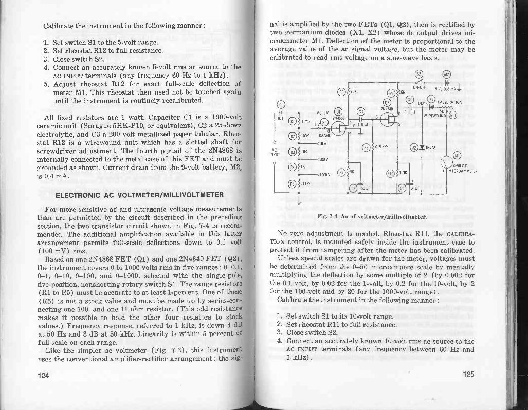
Calibrate the instrument in the following manner :
1. Set switch 51 to the 5 -volt range.2. Set rheostat R12 to full resistance.3. Close switch S2.4. Connect an accurately known 5 -volt rms ac source to the
AC INPUT terminals (any frequency 60 Hz to 1 kHz) .5. Adjust rheostat R12 for exact full-scale deflection of
meter Ml. This rheostat then need not be touched againuntil the instrument is routinely recalibrated.
All fixed resistors are 1 watt. Capacitor C1 is a 1000 -voltceramic unit (Sprague 51 -1K -P10, or equivalent) , C2 a 25-dcwvelectrolytic, and C3 a 200 -volt metallized paper tubular. Rheo-stat R12 is a wirewound unit which has a slotted shaft forscrewdriver adjustment. The fourth pigtail of the 2N4868 isinternally connected to the metal case of this FET and must begrounded as shown. Current drain from the 9 -volt battery, M2,is 0.4 mA.
ELECTRONIC AC VOLTMETER/MILLIVOLTMETER
For more sensitive af and ultrasonic voltage measurementsthan are permitted by the circuit described in the precedingsection, the two -transistor circuit shown in Fig. 7-4 is recom-mended. The additional amplification available in this latterarrangement permits full-scale deflections down to 0.1 volt(100 mV) rms.
Based on one 2N4868 FET (Q1) and one 2N4340 FET (Q2),the instrument covers 0 to 1000 volts rms in five ranges : 0-0.1,0-1, 0-10, 0-100, and 0-1000, selected with the single -pole,five -position, nonshorting rotary switch 51. The range resistors(R1 to R5) must be accurate to at least 1 -percent. One of these(R5) is not a stock value and must be made up by series -con-necting one 100- and one 11 -ohm resistor. (This odd resistancemakes it possible to hold the other four resistors to stockvalues.) Frequency response, referred to 1 kHz, is down 4 dBat 50 Hz and 3 dB at 50 kHz. Linearity is within 5 percent offull scale on each range.
Like the simpler ac voltmeter (Fig. 7-3), this instrumenuses the conventional amplifier -rectifier arrangement : the si
124
nal is amplified by the two FETs (Q1, Q2), then is rectified bytwo germanium diodes (X1, X2) whose dc output drives mi-croammeter Ml. Deflection of the meter is proportional to theaverage value of the ac signal voltage, but the meter may becalibrated to read rms voltage on a sine -wave basis.
0 . 1 80
INPUTAC C)
1 MQ1V
0.1V2N4868
100K
10K
1K
1115)
G
RANGE
10 V
100 V
20K
2N4340
G
P c 1.0 NF
1 000 V 0
s
5K
0 500F
0.5 Mf2
0 09 V. 0.8 rri7ON -OFF
A4--OK
0 1N 4AC) CALIBRATION
D 1.0 pF
3.3K
0 50 pF
Fig. 7-4. An af voltmeter/millivoltmeter.
0-50 DCM I CROAMMETER
No zero adjustment is needed. Rheostat R11, the CALIBRA-TION control, is mounted safely inside the instrument case toprotect it from tampering after the meter has been calibrated.
Unless special scales are drawn for the meter, voltages mustbe determined from the 0-50 microampere scale by mentallymultiplying the deflection by some multiple of 2 (by 0.002 forthe 0.1 -volt, by 0.02 for the 1 -volt, by 0.2 for the 10 -volt, by 2for the 100 -volt and by 20 for the 1000 -volt range).
Calibrate the instrument in the following manner :
1. Set switch Si to its 10 -volt range.2. Set rheostat R11 to full resistance.3. Close switch S2.4. Connect an accurately known 10 -volt rms ac source to the
AC INPUT terminals (any frequency between 60 Hz and1 kHz).
125

5. Adjust rheostat R11 for exact full-scale deflection ofmeter Ml. The rheostat then need not be touched againuntil the meter is routinely recalibrated.
All fixed resistors are 1 watt. Capacitor C1 is a 1000 -voltceramic unit (Sprague 5HK-P10, or equivalent), C3 is a 200 -volt metallized paper tubular, and C2 and C5 are 25-dcwv elec-trolytics. Rheostat R11 is a wirewound unit which has a slot-ted shaft for screwdriver adjustment. The fourth pigtail of the2N4868 (Q1) is internally connected to the metal case of thisFET and must be grounded as shown, but the gate electrodeof the 2N4340 (Q2) is internally connected to the metal caseof the latter FET, which accordingly must be kept clear ofcontact with wiring, chassis, and other components. Currentdrain from the 9 -volt battery, M2, is 0.8 mA.
The terminal arrangement for the FETs is shown in Appen-dix A. Manufacturers of FETs can be obtained from Appen-dix B.
CRYSTAL DUAL -FREQUENCY STANDARD
Fig. 7-5 shows the circuit of a dual crystal oscillator withoutput selectable at either 100 or 1000 kHz. Both signals givestrong harmonics for calibration purposes far into the high -frequency spectrum. The circuit is based on a single 2N3823FET.
A dpdt FREQUENCY SELECTOR switch (S1A-S1B) connects the100 -kHz crystal and the first tank (L1-05) into the circuit for100 -kHz output, or the 1000 -kHz crystal and the second tank(L2 -C6) into the circuit for 1000 -kHz output. The tank coilsare slug tuned for maximum output signal, as indicated by anac vtvm or transistorized electronic ac voltmeter connected tothe RF OUTPUT terminals. (L1 is a Miller No. 42A223CBI, orequivalent; L2 is a Miller No. 42A335CBI, or equivalent.) Eachcrystal frequency is adjustable over a narrow range by meansof a 50-pF trimmer capacitor (C1, C2) to standardize the out-puts against WWV transmissions or other standard -frequencysignals.
All wiring must be kept as short, direct, and rigid as prac-tical. Also, wiring should be kept well away from metal chassisor case, to minimize stray capacitance which will bypass
126
higher harmonics of the signals. Capacitors C3, C4, and C7are mica; C5 and C6 are silvered mica. The fourth pigtail ofthe 2N3823 is internally connected to the metal case of thisFET and must be grounded as shown. Current drain from the6 -volt battery, Ml, is 0.8 mA.
CIA,0
100 kHz 1000 kHz
XTAL-1MT
GAL-
,.(1000
(100 kHz) kHz)
2
50 pF
02N3823
0 470K
FREQUENCY SELECTOR
J_
1001
1.7-2.9 pH
1000 kHz0
.001
ON -OFF
Fig. 7-5. Crystal dual -frequency standard.
0.0001
6V0.8 mA
RF
OUTPUT
9
100-kHz/10-kHz SECONDARY FREQUENCY STANDARD
The secondary frequency standard circuit shown in Fig. 7-6has a 100 -kHz oscillator and 10 -kHz multivibrator. This ar-rangement provides 100 -kHz harmonics far into the high -frequency spectrum, and each 100 -kHz interval is subdividedby harmonics of the multivibrator. The oscillator is based on asingle 2N3823 FET (Q1) and the multivibrator on two 2N4340FETs (Q2, Q3).
The oscillator is tuned to the crystal frequency by adjustingthe slug -tuned coil, L1 (Miller No. 42A223CBI, or equivalent),and the crystal frequency is adjustable over a narrow rangeby means of 50-pF trimmer capacitor C1, to standardize the100 kHz against WWV transmissions or other standard -fre-quency signals. The 100 -kHz output is capacitance coupledthrough capacitor C3.
127

XTAL(100 kHz)
Ql
2N3823OSCILLATOR
(2)4470K
07,
100 kHz OUTPUT
1I
0-.0001
DC
8 2K
1. 7-
-2.90
10 kHz OUTPUT
7A).1.00017
10K
C8 C9
i4XLI2MULT !VIBRATOR . 002
D 02N4340 0 2N4340
WI REWOUND
20K
C25K
SK
10 kHz
ADJUST
Fig. 7-6. 100-kHz/10-kHz secondary frequency standard.
0:\10 kHz
ON -OFF
Synchronizing 100 -kHz voltage is injected into the multi -vibrator through potentiometer R5 which, with R4, forms thegate resistor of FET Q2. The 10 -kHz output is capacitancecoupled through capacitor C6.
The multivibrator is best adjusted by connecting the 100 -kHz output of the instrument to a communications receiver,closing switch S1, and adjusting potentiometer R5 until ex-actly nine intermediate (10 -kHz) signals can be counted be-tween each two adjacent 100 -kHz. harmonics. Adjustment ofR5 will cause the intermediate points to jump abruptly fromone number to another as the multivibrator synchronizes at 7,8, 9, 10, or 11 kHz. When the 10 -kHz harmonics are not wanted,switch S1 may be opened, and only the 100 -kHz harmonics willremain.
The 10 -kHz fundamental is separately available, through ca-pacitor C6, as a highly accurate audio frequency, as a squarewave, and as a synchronizing signal.
All wiring must be kept as short, direct, and rigid as prac-tical. Also, wiring should be kept well away from metal chassisor case, to minimize stray capacitance which will bypass higherharmonics of the signals. All fixed resistors are 1/2 watt, andall fixed capacitors are silvered mica. Potentiometer R5 is wire -wound and provided with a slotted shaft for screwdriver ad -
128
justment ; it should be mounted safely inside the instrumentcase to protect it from tampering. The fourth pigtail of the2N3823 is internally connected to the metal case of this FETand must be grounded as shown. The gate electrode of the2N4340 is internally connected to the metal case in the latterFET, however, so both 2N4340s must be kept clear of contactwith each other or with wiring, chassis, or other components.Total current drain from the 6 -volt battery, Ml, is 2.2 mA.
DIRECT -READING AUDIO -FREQUENCY METER
A direct -reading audio -frequency meter is a convenient in-strument. Feed an unknown audio frequency into its input ter-minals and read the frequency directly from the meter scale.No adjustments of any kind need be made ; only the frequencyrange must be switched in the same way that a voltmeter rangeis switched.
Fig. 7-7 shows the circuit of such an instrument, based onone 2N4868 FET (Q1) and one 2N4340 FET (Q2) . This in-strument covers 0 to 100 kHz in four ranges : 0-100 Hz, 0-1kHz, 0-10 kHz, and 0-100 kHz. The frequency is indicated onthe scale of microammeter M1. The indication is independent
RANGES
A. 0 to 100 HzB. 0 to 1 kHzC. 0 to 10 kHzD. 0 to ICO kHz
SIGNALINPUT
(E)f2OK
02N4868
0 \ON-OFF
01 9V1.4 mA
A
0.1
.01
CALIBRATION CONTROLS
0
°---75 OKV2.1)
RANGE WOKD 7 LE2)
cf 6.0OA 0 B
1534A
Fig. 7-7. Direct -reading audio -frequency meter.
0-50 DC
MICROAMMETER
129

of signal amplitude from 1.7 volts rms upward and is inde-pendent of waveform over a wide range. The response is lin-ear; hence, only one point need be calibrated in each frequencyrange.
The circuit exploits the same principle employed in sometube -type frequency meters : It is essentially two overdrivenamplifier stages in cascade. The output of the last stage accord-ingly is a square wave which is applied to an RC circuit (R6 -R9 and C4 -C7) and diode rectifiers X1 and X2. Since the squarewave is limited (i.e., of constant amplitude), the deflection ofmeter M1 depends only on the number of pulses passingthrough this meter during each second, so is directly propor-tional to the pulse frequency.
The frequency meter must be calibrated at one point in eachof its four ranges (the best point is the top frequency in eachrange). Rheostats R6, R7, R8, and R9 are the CALIBRATIONcontrols, and these units are provided with slotted shafts fora screwdriver. They are also mounted safely inside the instru-ment case to protect them from tampering. Follow this calibra-tion procedure :
1. Close switch Si.2. Set range switch S2 to position A.3. Connect an accurate audio oscillator to the SIGNAL IN-
PUT terminals and set its output to 2 to 3 volts rms.4. Set the signal frequency to 100 Hz and adjust R6 for
full-scale deflection of meter Ml.5. Set S2 to position B.6. Set the signal frequency to 1 kHz and adjust R7 for full-
scale deflection of the meter.7. Set S2 to position C.8. Set the signal frequency to 10 kHz and adjust R8 for
full-scale deflection of the meter.9. Set S2 to position D.
10. Set the signal frequency to 100 kHz and adjust R9 forfull-scale deflection of the meter.
All wiring must be kept as short, direct, and rigid as prac-tical. All fixed resistors are 1/2 watt. Capacitors C1 and C3 a400 -volt metallized paper tubulars, and C2 is a 25-dcwv eletrolytic. Capacitors C4 and C5 are 200 -volt metallized pap
130
tubulars, and C6 and C7 are silvered mica. While the rangecapacitors (C4 to C7) should be reasonably accurate, any de-viation in capacitance will be compensated by adjustment ofthe calibration controls (R6 to R9). The fourth pigtail of the2N4868 is internally connected to the metal case of this FETand must be grounded as shown. In the 2N4340, however, themetal case is internally connected to the gate electrode, so thislatter FET must be kept clear of contact with wiring, othercomponents, or chassis. Current drain from the 9 -volt battery,M2, is 1.4 mA.
4.5 -MHz SOUND -MARKER GENERATOR
Fig. 7-8 shows the circuit of a 4.5 -MHz crystal oscillator forsound -channel alignment in tv receivers. This oscillator, basedon a single 2N3823 FET, is tuned to the crystal frequency byadjusting the slug -tuned tank coil, Li (Miller No. 42A335CBI,or equivalent), for maximum output, as indicated by a com-munications receiver or an rf voltmeter connected to the RFOUTPUT terminals.
Fig. 7-8. Television sound -marker generator (4.5 MHz).
The open -circuit signal amplitude at the RF OUTPUT termi-nals is 4.0 volts rms when the dc supply is 6 volts at 1.4 mA.The signal strength may be continuously adjusted by makingC4 a 50-pF midget variable capacitor.
Resistors R1 and R2 are 1/2 watt. Capacitors Cl, C2, andC4 are mica, and capacitor C3 is silvered mica. The fourth pig -
131

tail of the 2N3823 is internally connected to the metal case ofthis FET and must be grounded as shown.
VARIABLE -FREQUENCY AUDIO OSCILLATOR
Fig. 7-9 shows the circuit of a variable -frequency RC -tunedaudio oscillator employing two 2N4340 FETs. Using the Wien -bridge frequency -determining network, this instrument covers20 Hz to 200 kHz in four ranges : 20-200 Hz, 200-2000 Hz, 2-20 kHz, and 20-200 kHz. Tuning in each range is accomplishedwith a dual 365-pF variable capacitor (C2), and ranges arechanged by switching identical resistors in pairs (R1 -R5, R2 -R6, R3 -R7, and R4 -R8). These resistances must be accurate toat least 1 percent.
A.
B.
C.
D.
RANGES
20 to 200 Hz
200 to 2000 Hz
2 to 20kHz 20
20 to MO kHz MO
5KOUTPUT
CONTROL
Fig. 7-9. Variable -frequency audio oscillator.
ON -OFF
sea0
22.5 V=0.8 mAI
10 piAF
OUTPUT
(i)
In this circuit there are two feedbacli paths, both throughcapacitor C4. One is through the bandswitched Wien bridge tothe gate of FET Q1 ; the other is through FEEDBACK ADJUSTrheostat R11 to the source of Q1. At the resonant frequency ofthe Wien bridge, the feedback to the Q1 gate is positive andcreates oscillation. The feedback through R11, however, isnegative and, since it cancels the oscillation on all frequenciesexcept the bridge resonant frequency, is responsible for thevery low distortion of this type of circuit.
132
The amplitude of the negative feedback is adjustable withrheostat R11, and the amplitude of the driving voltage pre-sented to the feedback/output amplifier (Q2) is adjustablewith potentiometer R12. Optimum adjustment of rheostat R11and potentiometer R12 results in lowest distortion of the out-put signal.
The low -impedance, source -follower output is adjustablewith potentiometer R14 from approximately zero to 0.4 voltrms. Current drain is 0.8 mA from the 22.5 -volt battery, Ml.Higher output amplitude (at the same current drain for theoscillator) may be obtained with an additional output -amplifierstage.
The tuning capacitor (C2) must be insulated from the metalchassis and should be enclosed in a grounded shield box. Thelower section of this capacitor is grounded, but the upper sec-tion floats and must be compensated with the 50-pF trimmercapacitor, C1. Solid construction must be employed through-out, and all wiring must be short, direct, and rigid.
The oscillator may be calibrated in the conventional manneragainst any available standard audio frequency, using an oscil-loscope set up for Lissajous figures. Another method makes useof a calibrated audio -frequency meter (see an earlier sectionof this chapter) connected to the AF OUTPUT terminals. Withswitch S1 set to the proper range, capacitor C2 is adjusted toresonance with the standard frequency (or to the desired fre-quency, as indicated by the audio -frequency meter). The dialof this tuning capacitor then is set to that frequency. Trimmercapacitor C1 is adjusted for continuous oscillation throughoutthe range.
Rheostat R11 is adjusted for constant output over the entirerange of the oscillator, as indicated by an electronic ac volt-meter or oscilloscope connected to the AF OUTPUT terminals. Po-tentiometer R12 is adjusted for minimum distortion (as indi-cated by an oscilloscope or distortion meter connected to theAF OUTPUT terminals). After adjustment, these two variableresistors need not be touched again until the instrument isroutinely rechecked.
All fixed resistors are 1 watt. Capacitors C4 and C5 are 50-dcwv electrolytics, and capacitor C3 is a 200 -volt metallizedpaper tubular. Rheostat R11 and potentiometer R12 have slot-ted shafts for screwdriver adjustment and are mounted safely
133

inside the instrument case to protect them from tampering,Trimmer capacitor Cl is also inside the case, being securelyfastened to the frame of tuning capacitor C2. The gate elec-trode of the 2N4340 is internally connected to the metal caseof this FET, so both 2N4340s must be kept clear of contactwith each other, other components, wiring or chassis.
DIP OSCILLATOR
The tube -type grid -dip oscillator is a well-known and usefulinstrument which needs no theoretical explanation nor a reci-tation of its merits here. Previously, some transistorized ver-sions of this device, while offering freedom from the powerline, have been less satisfying than the tube type, since the bi-polar transistor reduced sensitivity and selectivity of the cir-cuit. With an FET, however, the dip oscillator behaves just asit does with a tube, because the gate -to -ground impedance ofthe FET is comparable to the grid -to -ground impedance of thetube. Response is sharp and fast, and the indicating meter neednot be connected in some special part of the circuit differentfrom the grid circuit of the tube.
Fig. 7-10 shows the circuit of a dip oscillator, based on a2N3823 FET. With six plug-in coils, this instrument covers therange 1.1 to 95 MHz: (A) 1.1-2.5 MHz, (B) 2.5-5 MHz, (C)5-11 MHz, (D) 10-25 MHz, (E) 20-45 MHz, and (F) 40-95MHz. The circuit is that of a Colpitts oscillator tuned with adual 100-pF variable capacitor, C1..
Dip is indicated by the 0-50 dc microammeter, Ml, in thegate -to -ground leg, and the meter sensitivity is adjustable withrheostat R1. Downward deflection is sharp when the tank (L1 -C1) is tuned to the resonant frequency of an external LC cir-cuit to which the tank is loosely coupled.
Like other dip oscillators, the one shown in Fig. 7-10 is usefulfor checking signals as well as dead LC circuits. A closed-circuit jack, J1, is provided for high -resistance magnetic head-phones used for this purpose. When the headphones are pluggedin, the microammeter is automatically disconnected from thecircuit.
The instrument may be calibrated in either of two ways : (1)Loosely couple L1 to a succession of dead LC tank circuitswhose frequencies are accurately known, tune Cl successively
134
for dip at the various frequencies, and mark the dial of thisvariable capacitor correspondingly. (2) With headphonesplugged into jack J1, tune in a number of accurately knownsignals, adjusting Cl for zero beat at each frequency and mark-ing the dial of the tuning capacitor correspondingly.
For stability, the instrument must be solidly constructed,and the shortest, most direct, and most rigid wiring practicalmust be used. All coils are tightly wound on 1 -inch -diameter
$ plug-in forms (see Table 7-1 for coil -winding data) . The num-
0PLUG-IN COIL(SEE TABLE 7-11
HEADPHONES
200 pF 02N3823
Fig. 7-10. Dip oscillator.
.001
1K
Sl
ON -OFF
@6V5 mA
ber of turns in the coils may need some adjustment to compen-sate for stray capacitance in an individual instrument and forthe particular gate -to -source capacitance of an individual FET.Resistor R2 is 1/2 watt, and capacitors C2, C3, and C4 aresilvered mica. The fourth pigtail of the 2N3823 is internallyconnected to the metal case of this FET and must be groundedas shown. Current drain from the 6 -volt battery (M2 in Fig.7-10) is 5 mA.
The steady deflection of the microammeter does not have thesame value on all frequency ranges and may even change to ahigher or lower value as the instrument is tuned through asingle range. Adjustment of rheostat R1, however, enables theoperator to set the pointer of M1 to a desirable point on thescale before tuning for dip. This rheostat also provides somedegree of volume control when the instrument is used withheadphones.
135

Table 7-1. Coil -Winding Data*
Coil Frequency Range Specifications
A 1.1-2.5 MHz 150 turns No. 32 enameled wire, closewoundB 2.5-5 MHz 77 turns No. 28 enameled wire, closewoundC 5-11 MHz 35 turns No. 22 enameled wire, closewoundD 10-25 MHz 17 turns No. 22 enameled wire, spaced to
winding length of 1 inchE 20-45 MHz 8.5 turns No. 22 enameled wire, spaced to
winding length of 1 inchF 40-95 MHz 41/2 turns No. 22 enameled wire, spaced to
winding length of 1 inch
All coils wound on Millen No. 45004 1 -inch, 4 -pin coil forms. or equivalent (use two ofthe pins).
AF MILLIAMMETER
Fig. 7-11 shows the circuit of an audio -frequency milli -ammeter, based on a single 2N4868 FET (Q1), which coversthe current range 0 to 500 mA in seven full-scale ranges : 0.5,1, 5, 10, 50, 100, and 500 milliamperes. A two -pole, seven -posi-tion rotary selector switch (S1) switches in the appropriatevalues of shunt resistance (R1 to R7) . The double -pole switch-ing guarantees that the circuit is never exposed to excessivecurrent between switch positions. Linearity of response iswithin 5 percent of full scale. Frequency response, referred to
RANGE
19V
ON-OFF
0.4 mA
Fig. 7-11. An af milliammeter.
136
NAA,A,25K CALIBRATION
W. W. CONTROL
0-50 DCMI CROAMMETER
1 kHz, is down 3.5 dB at 50 Hz and 2 dB at 50 kHz. Currentdrain is 0.4 mA at 9 V dc.
Input -resistance values are : 0.5 mA, 1000 ohms ; 1 mA, 500ohms ; 5 mA, 100 ohms ; 10 mA, 50 ohms ; 50 mA, 10 ohms ; 100mA, 5 ohms ; and 500 mA, 1 ohm.
Like the af millivoltmeters described earlier in this chapter,this circuit uses the conventional amplifier -rectifier arrange-ment : the signal is developed by current through the selectedshunt resistors and is first amplified by the FET and then recti-fied by the two germanium diodes (X1, X2) . The dc output ofthe diodes is more than sufficient to drive microammeter M1 tofull scale. The meter deflection is proportional to the averagevalue of the input af current, but the meter may be calibratedto read rms current on a sine -wave basis.
No zero adjustment is needed. Rheostat R11, the CALIBRA-TION control, is mounted safely inside the instrument case toprotect it from being turned by accident after the instrumenthas been completely calibrated.
The 0- to 50 -dc microampere scale of meter M1 reads directlyon the 50-mA range, and is easily read on the 0.5-, 5-, and 500-mA ranges by mentally shifting the decimal point as required.On the 1-, 10-, and 100-mA ranges, however, the reading mustbe mentally multiplied by 2 or some multiple of 2 (thus, by0.02 for the 1-mA, by 0.2 for the 10-mA, or by 2 for the 100-mA range of the af milliammeter).
Calibrate the instrument in the following manner :
1. Set switch S1 to the 50-mA range.2. Set rheostat R11 to full resistance.3. Close switch S2.4. Connect an accurately known 50-mA ac source to the AF
INPUT terminals (any frequency between 60 Hz and 1kHz).
5. Adjust rheostat R11 for exact full-scale deflection ofmeter Ml. This rheostat then need not be touched againuntil the instrument is routinely recalibrated.
The instrument is now in calibration on all ranges if accuratevalues have been used for resistors R1 through R7.
All fixed resistors are 1 watt. (The range resistors-R1 toR7-must be accurate to at least 1 percent.) Capacitor C1 is
137

a 25-dcwv electrolytic ; C2 is a 100-volt plastic unit. RheostatR11 is a wirewound unit provided with a slotted shaft forscrewdriver adjustment.
For stability, all wiring must be as short, rigid, and directas practical ; and the fourth pigtail of the 2N4868, which is in-ternally connected to the metal case of this FET, must begrounded as shown, for shielding.
INDUCTANCE CHECKER
Any inductance between 60 /LH and 60,000 H may be
checked by the resonance method, using the circuit shown inFig. 7-12 with a variable -frequency audio oscillator. With theunknown inductance connected to terminals X -X, the oscil-lator is tuned for peak deflection of meter Ml, whereupon theinductance is determined (in terms of the .01-µF capacitance,C3) by calculation or by reference to the graph in Fig. 7-13.
In this circuit (Fig. 7-12), the U183 FET (Q1) serves as asource follower between the oscillator and the measuring cir-cuit. The advantages of this arrangement are : (a) the highinput impedance of the resultant circuit reduces oscillator load-ing to virtually zero, and (b) the follower isolates the measur-ing circuit (M1 -X1 -C3 -L,) from the signal source.
Potentiometer R1 allows adjustment of the gain for exactfull-scale resonant deflection of meter Ml. This is an addedconvenience even when the audio oscillator has its own outputcontrol. With R1 set for maximum gain, an oscillator output of
U183
G
OSCILLATOR INPUT
+ 9V3.3 mA
ON -OFF
100 vFC 0-50 DC
0 MICROAMMETER 0
.01
Fig. 7-12. Inductance checker.
138
bxTO UNKNOWN INDUCTANCE
X (Lx)
1.5 volts rms will drive meter M1 to full scale with most in-ductors which will be connected to terminals X -X. Dc micro-
ammeter M1 is made to respond to alternating current simplyby connecting the 1N34A germanium diode (X1) in parallelwith it. Current drain of the circuit is 3.3 mA at 9 V dc.
INDUCTANCE (HENRYS)
0.01 100 10,000.
0.001 0.1 10 1000
OAX101 0.01 100
0.00001 0.001 0.1 10
\\\10 100 200
FREQUENCY
(Hz(
100 1000 2000
1000 10K 20K
10K 100K 200K
Fig. 7-13. Inductance chart.
Resistor R2 is 1/2 watt. Capacitor Cl is a 100 -volt plasticunit; C2 is a 25-dcwv electrolytic. For stability and accuracy,C3 must be a silvered mica capacitor as close as practical tothe rated .01 /IF, since it is with reference to this capacitancethat the unknown inductance is determined.
The checker must be built mechanically solid, and all wiringmust be as short, rigid, and direct as possible. A fourth pigtail
139

of the U183 is internally connected to the metal case of thisFET and must be grounded as shown, for shielding.
To use the checker :
1. Connect a variable -frequency audio oscillator (tuningrange: 20 to 200,000 Hz) to the OSCILLATOR INPUT ter-minals.
2. Connect the unknown inductance (L,) to terminals X -X.3. Close switch Si, and switch on the oscillator.4. Starting at the bottom of the lowest frequency range,
tune the oscillator slowly throughout its ranges until asharp deflection of meter M1 occurs. Adjust the oscillatoroutput control and gain -control potentiometer R1 to bringthis deflection close to full scale of the meter.
5. At this point of peak deflection, read the frequency fromthe oscillator dial.
6. For close results, calculate the inductance :
1Lx (395 f2 x 10-9)
where,L, is the unknown inductance in henrys,f is the oscillator frequency in hertz.
7. For approximate results, eliminating calculations, use thechart given in Fig. 7-13.
SUBSTITUTION -TYPE CAPACITANCE METER
Small capacitances are accurately measured by means of thesubstitution process, since this method of measurement auto-matically compensates for stray capacitances in the test setup.It is advantageous to measure small capacitances (0.1 to 400pF ) at radio frequencies. Fig. 7-14 shows the circuit of a sub-stitution -type capacitance checker operated at 1 MHz.
This arrangement employs a 1 -MHz crystal oscillator basedon a 2N3823 FET (Q1). The fix -tuned oscillator tank (L1 -C2)is link -coupled to the resonant measuring circuit, which iscomposed of inductor L4, trimmer C4, variable capacitor C5,and unknown capacitance Cx connected to terminals X -X. Asimple rf voltmeter (consisting of germanium diode X1, rheo-stat R3, microammeter Ml, and rf bypass capacitor C6) is con -
140
0 MAIN ADJUSTMENT
EQL 6xTO UNKNOWN
F 10 pF 700 pF ? XCAPACITANCE
0 1N34AAUX LIARY
ADJUSTMENT
100K
T
SENSITIVITY
°°
Fig. 7-14. Substitution -type capacitance checker.
0-50 DCM I CROAMMETER
nected across the measuring circuit as a resonance indicator.Both C4 and C5 are provided with calibrated dials reading di-rectly in picofarads. The oscillator coil (L1) and the measur-ing -circuit coil (L4) are slug -tuned units (L1, adjusted to 250
Miller No. 20A224RBI ; L4, adjusted to 60 ttH, Miller No.41A685CBI) . Coils L2 and L3 are link -coupling coils whichmust be provided by the builder; each consists of two turns ofinsulated hookup wire closewound near the bottom ends of L1and L4, respectively.
All fixed resistors are 1/2 watt. Capacitors Cl, C3, and C6are mica ; C2 is silvered mica. All wiring must be short, direct,and rigid. Moreover, the wiring in the measuring circuit (i.e.,between L4, C4, C5, and terminals X -X) must be straight,solid No. 14 bus. A fourth pigtail of the 2N3823 is internallyconnected to the metal case of this FET and must be groundedas shown, for shielding. Total current drain is 12 mA at 15V dc.
After the assembly has been completed and the wiring veri-fied, the crystal oscillator must be initially adjusted :
1. Connect an rf vtvm between ground and the top of L1.2. Close switch Si.3. Adjust the L1 slug for peak deflection of the vtvm. This
slug need not be touched again except during routine re -calibration of the instrument.
Next, initially adjust the measuring circuit:
141

1. Set variable capacitor C4 to half capacitance and C5 tomaximum capacitance.
2. Set rheostat R3 to maximum resistance.3. Close switch S1.4. Adjust the L4 slug for peak deflection of meter M1, re-
ducing the resistance of R3 if necessary to ensure a read-able deflection. This slug need not be touched again ex-cept during routine recalibration of the instrument.
To use the checker :
1. Close switch Si, and resonate the circuit by setting C5 tomaximum capacitance and trimming with C4 for peak de-flection of meter M1. Thenceforth, do not touch C4.
2. Record the capacitance setting of C5 as Ca.3. Connect the unknown capacitance (C') to terminals X -X
by the shortest possible leads. This will detune the mea-suring circuit, and the meter deflection will either de-crease or disappear.
4. Retune C5 to restore resonance, as indicated by peak de-flection of Ml.
5. Record this new capacitance setting of C5 as Cb.
6. Calculate the unknown capacitance :
Cz=Ca-Cb
When long leads must be used to connect the unknown ca-pacitor to the instrument, install the leads first (in the sameposition they will take when the capacitor later is connected tothem) and then perform Steps 1 and 2. This automaticallycompensates for the lead capacitance. Then connect the un-known capacitor to the far end of the leads and perform Steps3 to 6 in the same manner described above.
When very small capacitances (0.1 to 1Q pF) are measured,all readings (Ca and Cb) should be taken from the dial of C4,and capacitor C5 should be used only to trim the circuit toresonance in Step 1. This step then consists of the followingprocedure:
1. Set C4 to maximum capacitance. Close switch Si, andtrim with C5 for peak deflection of meter Ml. Record thissetting of C4 as Ca, and thenceforth do not touch C5.
142
IMPEDANCE METER
Fig. 7-15 shows the circuit of an impedance meter that em-ploys a widely used principle of measurement : an af voltage isapplied to an unknown impedance (Z) in series with a cali-brated variable resistor (R), and the voltage drops (Ez and Er)across Z and R, respectively, are checked separately with anelectronic voltmeter while R is varied. When the voltage dropsare equal (i.e., Ez = E,.), Z = R and may be read directly fromthe calibrated dial of the variable resistor.
jMAIN
0 ciCONTROL
'' 10K W. W.,....=.....-..
1N34A 1.0 pF
O+
0-50 DC
M I CROAMMETER
X X
TOUNKNOWN IMPEDANCE
1N34A
slON -
OFF
9V0.4 mA
2N4868
G
Fig. 7-15. Impedance meter.
SENSITIVITY
In Fig. 7-15, rheostat R1 is the calibrated variable resistor(0 to 10,000 ohms) which is in series with the unknown im-pedance connected to terminals X -X. A signal voltage, derivedfrom an external audio oscillator, is applied to this series com-bination through input transformer Ti. The electronic volt-meter is composed of an af amplifier, based on a 2N4868 FET(Q1), followed by a two -diode rectifier (X1, X2) and a dcmicroammeter (M1). When switch S2 is in Position A, thisvoltmeter is connected across variable resistor R1 and readsEr; when S1 is in Position B, the voltmeter is connected acrossthe unknown impedance and reads Ez. The meter needs novoltage calibration, since it serves only to indicate referencepoints; the de scale of microammeter M1 may be used directlyfor this purpose. (It is necessary only to adjust R1 so that thedeflection is the same for each position of switch S2 ; the mag-
143

nitude of the deflection is inconsequential.) The input poten-tiometer (R5) of the voltmeter circuit allows the meter to beadjusted for deflection near full scale to increase accuracy.Current drain of the circuit is 0.4 mA at 9 V dc.
All fixed resistors are 1/2 watt. Rheostat R1 is wirewoundand must have a dial reading directly in ohms. Capacitors C1and C3 are 100 -volt plastic units ; C2 is a 25-dcwv electrolytic.Transformer T1 may be any convenient unit having a 1 :1, 2 :1,or 3:1 turns ratio, and preferably should be shielded.
All wiring must be as short, rigid, and direct as practical.Overall shielding is desirable but not mandatory. A fourthpigtailof the 2N4868 is internally connected to the metal case of thisFET and must be grounded as shown, for shielding.
Use this instrument in the following manner :
1. Connect an audio oscillator to the OSCILLATOR INPUTterminals (common test frequencies are 400, 500, and1000 Hz), switch it on, and set its output to a level thatwill not saturate transformer T1.
2. Connect the unknown impedance (Z,c) to terminals X -X.3. Set potentiometer R5 for maximum sensitivity.4. Close switch S1.5. Throw switch S2 to Position A, and adjust rheostat R1
and potentiometer R5 for a deflection near full scale ofmeter Ml. Note the meter reading.
6. Throw switch S2 to Position B and note the meterreading.
7. Adjust R1 to make the deflection the same as it was inStep 5.
8. Throw switch S2 back to Position A, note the deflection,and adjust R1 again, as in Step 7.
9. Continue this procedure until there is no change inmeter reading as S2 is thrown back and forth betweenA and B.
10. At this point, read the value of the unknown impedancefrom the ohms dial of rheostat R1.
HETERODYNE FREQUENCY METER
By means of the zero -beat method, radio frequencies far intothe spectrum may be spotted and measured with a calibrated
144
low -frequency rf oscillator. This is made possible by zero beat-ing between the unknown frequencies and harmonics of thecalibrated oscillator. When a mixer and calibrated oscillatorare combined for this purpose in one unit, the result -is aheterodyne frequency meter.
Fig. 7-16 shows the circuit of a heterodyne frequency meterconsisting of a 1- to 2 -MHz oscillator (Q1), an untuned mixer(X1), and an af (beat -note) amplifier (Q2). The oscillatoremploys a 2N3823 FET; the mixer, a 1N34A germanium di-ode; and the af amplifier, a 2N3823 FET.
RF SIGNAL INPUTIX
50 pF-
1Q)
Fig. 7-16. Heterodyne frequency meter.
The oscillator is the Hartley type and is continuously tunableover the range of 1 to 2 MHz. The oscillator tank comprisescoil Li, 365-pF tuning capacitor C4, and 50-pF trimmer capaci-tor C3. Coil L1 consists of 65 turns of No. 28 enameled wireclosewound on a 1-inch-diameter form, with a tap taken at thetwentieth turn from the ground end. Coil L2 is a coupling coilconsisting of 10 turns of No. 28 enameled wire closewoundaround the center of Ll and insulated from the latter.
The oscillator output is coupled, through L2, into the diodemixer simultaneously with the unknown rf signal (coupledthrough capacitor C5). A beat note between the two signals is
145

generated in the mixer and is transmitted to the af amplifierthrough coupling capacitor C7. The latter also serves to blockthe diode dc component from the 2N3823 gate. Magnetic head-phones, plugged into jack J1, complete the 2N3823 drain cir-cuit and make the beat note audible. Other beat -note indicators,such as a vtvm, oscilloscope, magic -eye tube, or audio -frequencymeter, may be used, provided J1 is shunted by a 2000 -ohmresistor to complete the 2N3823 de circuit.
The instrument draws 6.5 mA at 9 V dc. This value is con-stant for zero signal and maximum signal.
All fixed resistors are 1/2 watt. Capacitors C1, C5, and C6are mica ; C2 is silvered mica. Capacitor C7 is a 100 -volt plas-tic unit, and C8 a 25-dcwv electrolytic.
The oscillator tuning unit (L1 -C3 -C4) must be stoutlybuilt, and the entire oscillator stage should be enclosed in agrounded shield box. All wiring must be as short, direct, andrigid as practical. A fourth pigtail of both the 2N3823s is in-ternally connected to the metal case of these FETs and must begrounded as shown, for shielding.
Main tuning capacitor C4 must be provided with a dial cali-brated to read directly in frequency -1000 to 2000 kHz. Oneway to calibrate this dial is to feed an accurate, unmodulated rfsignal -generator output into the RF SIGNAL INPUT terminals,set C3 to midcapacitance, set the generator successively to asmany frequencies as practical between 1000 and 2000 kHz, andat each frequency set C4 to zero beat (as indicated by head-phone signal) and inscribe the C4 dial with the correspondingfrequency. This calibration then may be checked more pre-cisely by replacing the generator with a 100 -kHz crystal oscil-lator, which will set up an accurate spot frequency each 100kHz across the C4 dial. To standardize the oscillator in thefuture, it is necessary only to feed in the 100 -kHz oscillator,set the C4 dial to its 1000 -kHz point, and, adjust trimmer C3for zero beat. Since C3 needs no constant adjustment, it shouldbe mounted inside the instrument case, where it will be safefrom disturbance, and should be provided with a slotted shaftfor screwdriver adjustment.
On second harmonics, the 1- to 2 -MHz C4 dial covers 2 to 4MHz, on twentieth harmonics 20 to 40 MHz, and so on. Simi-larly, on the second "subharmonic" the dial covers 500 to1000 kHz.
HARMONIC -DISTORTION METER
A harmonic -distortion meter is convenient for measuringthe total distortion of an audio amplifier, a component, or anetwork. A pure sine -wave signal is applied to the input of thedevice under test, and the distortion meter is connected to theoutput. The meter is tuned to suppress the fundamental fre-quency of the test signal. The self-contained electronic -volt-meter section of the instrument then is used to sample the out-put -signal voltage before and after the suppression. The firstvoltage contains the fundamental and harmonics, whereas thesecond one contains only the harmonics (distortion compo-nents introduced by the device under test). The total distor-tion therefore is the ratio of the second voltage to the first, andcan be expressed either as a decimal or as a percentage.
Fig. 7-17 shows the circuit of a complete distortion meteremploying these principles. This instrument covers the fre-quency range of 20 Hz to 20 kHz in three bands : (a) 20-200Hz, (b) 200-2000 Hz, and (c) 2-20 kHz. Ranges are selectedby double -pole, three -position switch S2. The filter circuit iscomposed of range resistors R7 to R12 and dual 400-pF tuningcapacitor C3. Within the amplifier comprising FETs Ql, Q2,and Q3, this RC network nulls sharply at the frequency towhich it is tuned, and allows signals at other frequencies topass relatively untouched in amplitude. The RC network alonetunes broadly, but its response is sharpened by overall nega-tive feedback around the amplifier through capacitor C5 andresistor R13. The voltmeter section comprises FET Q4, inputrange selector S4 and R17 -R20, and rectifier -type microam-meter (M1 -X1 -X2). Total current drain is 2.2 mA at 12 V dc.
The amplifier section is based on three 2N4340 FETs (Q1,Q2, Q3). This section is followed by an af voltmeter based on asingle 2N4868 FET (Q4). When switch S3 is in Position A,the voltmeter checks the signal voltage before the filter; andwhen S3 is in Position B, the meter checks the signal voltageafter the filter.
All fixed resistors are 1 watt. Resistors R2, R3, R5, R6 toR12, R14, R16, and R17 to R20 must be rated at 1 percent. Inan individual layout, R13 may need adjustment for sharpestnull response of the circuit. Capacitors Cl, C2, C4, C5, and C6are 100 -volt plastic units ; C7 is a 25-dcwv electrolytic. Each
146 147

Fig. 7-17. Distortion meter.
section of the dual 400-pF tuning capacitor (C3) has a built-intrimmer for initial adjustment.
After the instrument has been completed and the wiringverified, first the voltmeter section should be calibrated :
1. Set potentiometer R1 for maximum sensitivity.2. Set switch S3 to Position A.3. Set switch S4 to its 5 -volt position.4. Connect an accurately known 5 -volt (rms) source to the
AF INPUT terminals.5. Close switch Si.6. Adjust rheostat R24 for exact full-scale deflection of
microammeter Ml.
The voltmeter now is calibrated on all ranges if resistors R17to R20 are accurate. (R24 need not be touched again exceptduring routine recalibration.)
Next, the filter (tuner) should be adjusted:
1. Set potentiometer R1 for maximum sensitivity.2. Set switch S2 to Position A.3. Set switch S3 to Position B.4. Set switch S4 to its 1 -volt position.5. Connect a high-grade audio oscillator to the AF INPUT
terminals and set it to 200 Hz at 1 -volt rms output.6. Set tuning capacitor C3 to minimum capacitance.7. Close switch Si.8. By adjusting the trimmers on C3A and C3B, tune the cir-
cuit for full dip (null) of the M1 deflection. (Readjust R1and S4, as required, for readable meter response.)
9. Tune C3 successively to various other frequencies downto 20 Hz, inscribing the C3 dial accordingly. The filternow will automatically be calibrated on the two otherbands (B and C) if resistors R7 to R12 are accurate.
Use of the instrument is straightforward :
1. Connect a high-grade sine -wave audio oscillator to theinput of the device under test.
2. Connect the distortion meter to the output of the device.3. Set switch S2 to the appropriate frequency range.
148
AL_149

4. Close switch S1.5. Set switch S3 to Position A.6. With switch S4 in the appropriate voltage position, ad-
just potentiometer R1 for full-scale deflection of meterM1.
7. Record this voltage as El.8. Set switch S3 to Position B.9. Tune capacitor C3 for null, and set S4 to successively
lower ranges for accurate reading of the voltage at null.10. Record the residual null voltage as E2.1.1. Calculate the distortion percentage :
E,D % = 100 =E,
Under certain conditions, the instrument may be direct read-ing in distortion percentage, requiring no calculations. Thus, ifE, is 1 volt, this point may be regarded as 100 percent. Thedistortion percentages at null then may be read directly ; e.g.,0.01 volt = 1 percent, 0.1 volt = 10 percent, and so on.
AF RF SIGNAL TRACER
The high input impedance of the FET makes possible for thefirst time a transistorized signal tracer which is fully com-petitive with the tube -type tracer. Basically, the signal traceris a high -gain af amplifier which drives a visual signal -strengthindicator and a speaker, and to which may be attached either asimple test probe for af input or a demodulator probe for a -mrf input.
Fig. 7-18 shows the circuit of a signal tracer employing twofield-effect transistors (Q1, Q2) and three npn bipolar transis-tors (Q3, Q4, Q5) . High sensitivity is provided by the frontend, which consists of an RC -coupled audio amplifier based onone 2N4868 FET (Q1) and one 2N4340 FET (Q2) . The afprobe or rf probe, as required, is plugged into this amplifierthrough concentric jack J1. The front-end amplifier drives me-ter M1 through germanium diodes X2 and X3. This providesthe visual indication of signal strength.
For aural indication of signal strength, a speaker is drivenby the power amplifier consisting of a driver stage (based on a2N169A transistor, Q3) and a push-pull Class -B output stage
150
Fig. 7-18. An af rf signal tracer.
151

(based on two 2N169A transistors, Q4 and Q5). The latterstage delivers 100 milliwatts to the speaker.
Switch S1 allows the speaker section to be turned off whenthe silent, visual indication provided by the meter is sufficient.At 9 V dc, the signal tracer draws a zero -signal current of 11mA whether the speaker is on or off, and a maximum -signalcurrent of 25 mA when the speaker is on and 11 mA when itis off.
All fixed resistors are 1/2 watt. Capacitor C1 is a 500 -voltceramic unit, while C2, C4, C6, and C7 are 100 -volt plastic orpaper units. Capacitors C3 and C5 are 25-dcwv electrolytics.
The layout is not critical ; however, all wiring must be asshort and direct as possible, to minimize stray coupling andinterference. For shielding, the entire unit must be enclosedin a metal box.
The instrument needs no calibration ; since response of themeter section is linear, the readings of microammeter M1 maybe taken directly as indications of signal strength, as long asthe setting of gain -control potentiometer R5 is undisturbedduring a measurement.
GEIGER COUNTER
Fig. 7-19 shows the circuit of a simple Geiger counter basedon one 2N4338 FET (Q1) and one 2N4868 FET (Q2). Basi-cally, this instrument is a high -gain RC -coupled of amplifierfollowed by an ac meter circuit (coupling capacitor C4, germa-nium diodes X1 and X2, microammeter Ml, and high -capaci-tance meter capacitor C6). A jack (J1) also is provided foralternate use of headphones ; and since this is a closed-circuitjack, withdrawal of the phone plug automatically switches themeter back into the circuit. Current drain is 0.6 mA at 12 V dc.
The amplifier receives its input signal from a Victoreen1B85 G -M tube (V1) biased by 900 V de (less than 10 mA).This is a beta -gamma particle counter. The type of self-con-tained supply selected for this high voltage will depend on theexpense to which the builder can go. It can vary from three300 -volt photoflash batteries (Eveready No. 493, or equivalent)connected in series, to one of the factory -built, miniature, dry -battery -operated high -voltage modules. Between these limitsare numerous build -it -yourself units operated from flashlight
152
Oil12V
ONO.6OmFAF
DANGER ! HIGH VOLTAGE
Fig. 7-19. Geiger counter.
HEADPHONE JACK
0-50 DCM I CROAMMETER
cells (1.5 to 6 volts) of the transistor -oscillator, buzzer, orpush-button-and-capacitor types. The ON -OFF switch in thehigh -voltage supply must be ganged with the instrumentswitch, S1.
All fixed resistors are 1/2 watt. Capacitor C1 is a 1000 -voltceramic unit; C3 and C4 are 100 -volt plastic; and C2, C5, andC6 are 25-dcwv electrolytics. All wiring must be short and di-rect. The gate electrode is internally connected to the case ofthe 2N4338 (Q1), so this FET must be mounted clear of wir-ing, chassis, and other components. A fourth pigtail of the2N4868 (Q2) is internally connected to the metal case of thisFET and should be grounded as shown, for shielding.
The count -rate range of the instrument may be determinedby exposing the 1B85 tube to various calibrated radioactivesamples, noting the corresponding deflections of meter Ml, andgraduating the scale of the meter accordingly.
ELECTROSCOPE
Fig. 7-20 shows the circuit of a simple electronic electro-scope. Unlike the traditional electroscope, this instrument em-ploys a 0-50 de microammeter (M1) instead of the familiargold leaves. The active element is a 2N4868 FET (Q1).
153

POLISHED BRASS BALL
0III{
0
CASE - 9V, 3mA
Fig 7-20. Electroscope.
ON -OFF
The circuit is a dc amplifier of the type used in single-FETelectronic voltmeters. The gate of the FET floats, however,having no external connection to ground; it is therefore verysusceptible to voltage pickup via stray capacitance coupling.The gate is connected to a smooth metal rod tipped by a smallpolished brass ball, the pickup element. The rod emerges fromthe metal case of the electroscope through a wide hole insulatedwith polystyrene.
The static drain current of the FET is balanced out of themeter by setting potentiometer R2 for zero deflection, withthe pickup ball clear of the operator's body or any other ob-
ject. When a charged body is then brought near the ball, orvice versa, the meter deflection is proportional to the charge in-
tensity and the distance. The response is sensitive enough thatthe electroscope is vigorously actuated by stroked paper, a j ust-used comb, the high -voltage points -in a tv receiver, and simi-lar charged bodies.
The circuit draws approximately 3 mA from the self-con-tained 9 -volt transistor battery, M2.
154
1N34A
STRIPE
A
2N169A
E B C
2N3819
S G D
APPENDIX .A
Terminal Guidefor Diodes andTransistors
1N295
TRIPES
K
2N 333
C
2N3823
CASE
(CASE)
1N3605 HEP R0052
STRIPE STRIPE
------F._A K A
2N2608
D
2N4118
CASE
2N2712
2N4338
G (CASE)
155

2N4340
G (CASE)
HEP F0015
D S G
156
2N4868
G
CASE G2
REP F1036
D
U183
G
CASE
CASE
40823
Cl
HEP 50015
U222
G (CASE)
HEP F0010
G
S1M
CASE
APPENDIX R
Manufacturers ofSemiconductors1N34A1N2951N36052N169A2N3332N26082N27122N38192N38232N41182N43382N43402N486840820HEP F0010HEP F0015HEP F1036HEP R0052HEP 50015S1MU183U222
GEGEGEGEGE, Texas InstrumentsSiliconixGETexas InstrumentsTexas InstrumentsSiliconixSiliconixSiliconixSiliconixRCAMotorolaMotorolaMotorolaMotorolaMotorolaInternational RectifierSiliconixSiliconix
157

Index
Acaf relay, sensitive, 110-111millivoltmeter, electronic, 124-126rf relay, 102-104voltmeter, electronic, 122-126
Age amplifier, 39-40All -wave regenerative receiver,
65-66Amplified photocell, 105-106Amplifier
100 -MHz grounded gate, 85-86455 kHz i-f, 37-38audio agc, 39-40auxiliary headphone, 38common source, 31dc, 40-41LC -tuned bandpass af, 31modulated light, 113-114notch af, 34-36push-pull final, 84-85RC coupled af, 23-24
tuned bandpass af, 32-34squelch, 73-74transformer -coupled af, 24-26two -stage af, 23-26video, 36
Audioagc amplifier, 39-40frequency meter, 129-131mixer, dual channel, 30-31oscillator, variable -frequency,
132-134preamplifier, high gain, 27squelch amplifier, 73-74
Auxiliary headphone amplifier, 38
Background of FET, 11Balanced
electronic dc voltmeter, 119-122modulator, 90-91
Bandpass af amplifierLC tuned, 31RC tuned, 32-34
Beat -frequency oscillator, 68-69Bipolar, 14
transistor, 26
158
Broadcast receiverregenerative, 64superhet, 61-63
Buffer for vfo, 98-99
Capacitance meter, substitutiontype, 140-142
Cascaded, 24Cascode preselector, 77Channel, 12Checker, inductance, 138-140Code -practice oscillator, 57-58Colpitts af oscillator, 56-57Common -source amplifier, 31Constant -current source, 109-110Conventional
crystal oscillator, 53-54phase inverter, 28-29
Convertercrystal controlled, 67-68single frequency, 67-68
Counter, geiger, 152-153Crystal
controlled converter, 67-68transmitter, 80-82
dual -frequency standard, 126-127oscillator, 100 -kHz, 55-56
conventional, 53-54Pierce, 54-55
Current drain, 31Cw monitor, 91-92
Dcamplifier, 40-41relay, 101-102voltmeter, balanced electronic,
119-122electronic, 118-119
Detectordrain, 74infinite impedance, 75-76modulated light, 113-114
Dip oscillator, 134-136Direct -reading meter, 129-131Doubler, push -push, 87-88
Drain, 12coupled multivibrator, 50-51detector, 74
Dualchannel audio mixer, 30-31frequency standard, crystal,
126-127
Electronicac millivoltmeter, 124-126
voltmeter, 122-126de voltmeter, 118-119
balanced, 119-122Electroscope, 153-154Exciter, four band, 88-90False zero, 40FET
background, 11operation, 12-14performance, 14-15ratings, 16-17structure, 12-14transmitters, modulating, 92-93types, 17
Field effect, 9-11transistor, 9
Filter, notch, 33Final amplifier, push-pull, 84-85Flip-flop, 59Forward transconductance, 15Four -band exciter, 88-90Frequency
meter, heterodyne, 144-146multiplier, single ended, 86-87standard, secondary, 127-129
Gates, 12Geiger counter, 152-153Generator, sound marker, 131Grounded -gate amplifier, 100 -MHz,
85-86
Harmonic -distortion meter, 147-150Headphone amplifier, auxiliary, 38Heterodyne frequency meter,
144-146High
gain audio preamplifier, 27impedance input, 26
I -f amplifier, 455 kHz, 37-38Impedance meter, 143-144Inductance checker, 138-140Infinite -impedance detector, 75-76Input, high impedance, 26Inverter
conventional phase, 28-29paraphase phase, 29-30
LC -tunedaf oscillator, 45-46bandpass af amplifier, 31
Low -gain af preamplifier, 20-21
Medium -gain af preamplifier, 21-22Meter
audio frequency, 129-131direct reading, 129-131harmonic distortion, 147-150heterodyne frequency, 144-146impedance, 143-144substitution -type capacitance,
140-142Milliammeter, af, 136-138Millivoltmeter, electronic ac,
124-126Mixer
dual -channel audio, 30-31rf, 76
Modulated -lightamplifier, 113-114detector, 113-114
Modulating FET transmitters,92-93
Modulator, balanced, 90-91Monitor
cw, 91-92phone, 95-97
Multiplier, single -ended frequency,86-87
Multivibratordrain coupled, 50-51source coupled, 51-52
Notchaf amplifier, 34-36filter, 33
Null, 33
Operation, FET, 12-14Oscillator
100 -kHz crystal, 55-56beat frequency, 68-69code -practice, 57-58Colpitts, 56-57conventional crystal, 53-54dip, 134-136LC tuned af, 45-46phase shift, 47-48Pierce crystal, 54-55self-excited, 52-53single frequency, 48-50transformer -feedback af, 43-45variable frequency, 97-98, 132-134Wien bridge, 48-50
Output -peak clipping, 31
Parallel -T network, 34Paraphase phase inverter, 29-30Performance, FET, 14-15
159
Phaseinverter, conventional, 28-29
paraphase, 29-30shift af oscillator, 47-48shifter, 114-115
Phone monitor, 95-97Photocell, amplified, 105-106Pierce crystal oscillator, 54-55Pinch -off voltage, 13Preamplifier
high -gain audio, 27low -gain af, 20-21medium -gain af, 21-22single -stage af, 20-22small -signal af, 19-20
Preselector, cascode, 77Push
-pull final amplifier, 84-85-push doubler, 87-88
Q -multiplier, 69-71
Ratings, FET, 16-17RC
coupled af amplifier, 23-24tuned bandpass af amplifier,
32-34Receiver
all -wave regenerative, 65-66regenerative broadcast, 64superhet broadcast, 61-63
Regenerativebroadcast receiver, 64receiver, all -wave, 65-66
Relayac rf, 102-104dc, 101-102sensitive ac af, 110-111sound operated, 111-113touch plate, 104-105
Resistor, voltage variable, 108-109Rf
mixer, 76relay, ac, 102-104
Secondary frequency standard,127-129
Selectojet, 71-73Self-excited rf oscillator, 52-53Sensitive ac af relay, 110-111Shifter, phase, 114-115Signal tracer, 150-152Single
-control TNT transmitter, 94-95ended frequency multiplier, 86-87frequency converter, 67-68
oscillator, 48-50stage af preamplifier, 20-22
transmitter, 80-82
160
Small -signal af preamplifier, 19-20Sound
marker generator, 131-operated relay, 111-113
Source, 12constant current, 109-110coupled multivibrator, 51-52follower, af, 22-23
Squelch amplifier, 73-74Standard
crystal dual -frequency, 126-127secondary frequency, 127-129
Structure, FET, 12-14Substitution -type capacitance
meter, 140-142Superhet broadcast receiver, 61-63Symmetrical FET, 12
Timer, 106-108TNT transmitter, single control,
94-95Touch -plate relay, 104-105Tracer, signal, 150-152Transconductance, forward, 15Transformer
coupled af amplifier, 24-26feedback af oscillator, 43-45
Transistorbipolar, 26field-effect, 9
Transmitter (s)crystal controlled, 80-82modulating FET, 92-93single -control TNT, 94-95
stage, 80-82two -stage, 82-84
Two -stageaf amplifier, 23-26transmitter, 82-84
Unipolar, 14
Variable -frequencyaudio oscillator, 132-134oscillator, 97-98
Vfo, 97-98buffer, 98-99
Video amplifier, 36Voltage
pinch -off, 13variable resistor, 108-109
Voltmeterbalanced electronic dc, 119-122electronic ac, 122-126
dc, 118-119
Wien -bridge oscillator, 48-50

Second EditionField-effect transistors (FETs) have become firmly establishedin solid-state electronics. New types of FETs have entered themarket, some of the original types are no longer manufactured,and additional applications have been added.
The distinctive feature of the FET that sets it apart from othertransistors is its high input impedance. Although it is a transistorby construction, it resembles a vacuum tube in operation.
This Look is devoted almost entirely to a discussion of actual,workable circuits using FETs. The book begins with a discussionof the fundamentals of the FET, such as background, structureand operation, performance, ratings, and types of FET's. Ampli-fiers and oscillators each have a chapter of their own. Practicalcircuits for broadcast -band and all -wave receivers make up an-other chapter. Transmitters with their accessory equipment aredescribed in detail. Another chapter covers relays, timers, andphase shifters. Various test instruments that can use FETs toadvantage in their circuitry are also covered. There are twoappendices in the back of the book that list FET manufacturersand provide drawings of basing diagrams for the FETs discussedin the book. These are primarily for those who wish to experi-ment with FETs on their own.
Technicians, hobbyists, and experimenters will find FETCircuits a valuable aid in their search for up-to-date information.
Rufus Turner is no stranger to readers of technical literature. A prolific -writer, he has over 2500 magazine articles and more than 40 books tohis credit. He earned his B.A. degree (with honors) at California StateUniversity at Los Angeles, and his M.A. and Ph.D. degrees at the Uni-versity of Southern California. He is as a registered professionalengineer in California and has had experience both in engineering andcollege teaching. Some of the other books by Dr. Turner are abc's ofCalculus, abc's of Electronic Power, abc's of FETs, abc's of IntegratedCircuits, abc's of Resistance and Resistors, abc's of Voltage -DependentResistors, abc's of Zener Diodes, Frequency and Its Measurement,Metrics for the Millions, RC Circuits, Solar Cells and Photocells, Solid -State Components, and Technical Writer's and Editor's Stylebook, allpublished by Howard W. Sams & Co., Inc.
$4.95/21439 (Replaces 20585)