22. VOLTAGE DEPENDENCE OF THIN DIELECTRIC BREAKDOWN
19
113 113 22. VOLTAGE DEPENDENCE OF THIN DIELECTRIC BREAKDOWN 22.1 Review/Background: In chapter 21, we summarized the essential features of gate dielectric breakdown (DB) such as it’s time dependent, voltage (not field) accelerated, correlated/uncorrelated, following Weibull distribution, soft vs hard breakdown. We extended the discussion about time dependent degradation. The physics of it is very similar to hot carrier (HCI), because it involves Si-O bond dissociation. The thickness of the thin gate oxide is ~ 1 nm (six atoms or radius of the single stranded DNA). How does it survive for so many years enduring trillions and trillions cycles [22.1]? That is what we want to answer. In this lecture, we will learn about voltage dependence of the dielectric breakdown. We will discuss how the defects are generated inside the gate oxide based on the Anode Hole Injection (AHI) model [22.2] and [22.3]. The theory in many ways will be similar to HCI, like carriers are hot, and there will be impact ionization. Only difference is: the impact- ionization takes place in anode (receiving electrode) instead of channel. We will verify the Anode Hole Injection model with comparing to the experiment data in several aspects: the effect of the oxide thickness, substrate bias, and gate bias polarity. 22.2 Dielectric lifetime of an IC and basic of voltage acceleration Estimation of dielectric lifetime of an IC is started with the smaller size test structure of area A TEST . The life time of the actual IC with area A IC is scaled according to the Eq. 22.1. In practice the industry cannot wait to see for 50% return, so they do the estimation for very small q%. When we drop the voltage by 1 V, how many orders of magnitude enhancement in lifetime we get: can be explained by the voltage acceleration factor γ , in Eq. 22.3.
Transcript of 22. VOLTAGE DEPENDENCE OF THIN DIELECTRIC BREAKDOWN

113
113
22. VOLTAGE DEPENDENCE OF THIN DIELECTRIC
BREAKDOWN
22.1 Review/Background:
In chapter 21, we summarized the essential features of gate dielectric breakdown
(DB) such as it’s time dependent, voltage (not field) accelerated, correlated/uncorrelated,
following Weibull distribution, soft vs hard breakdown. We extended the discussion
about time dependent degradation. The physics of it is very similar to hot carrier (HCI),
because it involves Si-O bond dissociation. The thickness of the thin gate oxide is ~ 1 nm
(six atoms or radius of the single stranded DNA). How does it survive for so many years
enduring trillions and trillions cycles [22.1]? That is what we want to answer. In this
lecture, we will learn about voltage dependence of the dielectric breakdown. We will
discuss how the defects are generated inside the gate oxide based on the Anode Hole
Injection (AHI) model [22.2] and [22.3]. The theory in many ways will be similar to HCI,
like carriers are hot, and there will be impact ionization. Only difference is: the impact-
ionization takes place in anode (receiving electrode) instead of channel. We will verify
the Anode Hole Injection model with comparing to the experiment data in several
aspects: the effect of the oxide thickness, substrate bias, and gate bias polarity.
22.2 Dielectric lifetime of an IC and basic of voltage acceleration
Estimation of dielectric lifetime of an IC is started with the smaller size test
structure of area ATEST. The life time of the actual IC with area AIC is scaled according to
the Eq. 22.1. In practice the industry cannot wait to see for 50% return, so they do the
estimation for very small q%. When we drop the voltage by 1 V, how many orders of
magnitude enhancement in lifetime we get: can be explained by the voltage acceleration
factor γ�,��� in Eq. 22.3.

114
114
���%� ��� � � ���� ��⁄ ��/����%� ����� 22.1
����%� ��� � ����1 � � 100⁄ ����1 � 0.5� # ���%� ��� 22.2
$%&'( � $)(%) � �*+ �10-./����% # 01,&223 22.3
In Fig. 22.1 (left) for very large gate bias empirical projection matches well with the
actual curve. However, once the operating bias converges to the safe operating voltage
we see that empirical observation is showing pessimistic behavior. In principle we can
use a slightly higher voltage to make faster computer, if we know the essential physics.
The right side plot shows the voltage acceleration factor which is the slope of the left
plot. Voltage acceleration factor is related with the IC lifetime through the Eq. 22.3.
Figure 22.1 Mean life time vs gate bias plot shows that lifetime increases with the
reduction of gate bias. Physics is important to understand the deviation of the actual
curve (blue) from the projection (red). (Right) The slope of the mean life time vs VG
curve known as voltage acceleration factor (γ) is plotted with respect to the gate bias. The
experimental data for oxides of different thickness from the literature (symbols) compare
quite well with the simulation results (solid line).

115
115
22.3 Anode hole injection (AHI) model
The anode hole injection model describes a physical process to explain the
defect generation inside the gate dielectric material [22.4]. According to this model,
carriers injected from the gate (substrate) undergo negligible energy loss as they travel
through the oxide and on reaching the substrate (gate) these high-energy (“hot”) electrons
cause impact ionization producing hot holes (See Fig. 22.2). The hot holes tunneling back
into the oxide increase the current density at localized spots, probably through hole-
induced trap generation, until the final runaway process leads to the catastrophic
breakdown. The term Anode Hole Injection (AHI) arises from old cathode tube
terminology. Cathode emits the particles and anode collects them. In this case gate
(substrate) emits electrons and substrate (gate) collects them and the degradation (defect
generation in the oxide) is due to the holes created at the anode.
If electron current J5, impact ionization coefficient γ66, and hole transmission
coefficient T8 are controlled by electric field (9), they can be represented as
:( � �;<=�� > 9⁄ � 22.4
0?? � @�;<=��@> 9⁄ � 22.5
�A � B�;<=��B> 9⁄ � 22.6
CD� � :(0??�A 22.7
��� � C × FD��G��� 22.8
������� ∝ ���C� ∝ 1/9 22.9

116
116
Fig. 22.2 (top) Anode-Hole Injection model. (Bottom left) high VGS: impact
ionization inside thick oxide is controlled by electric field. (Bottom middle)
medium VGS: electrons are so energetic, they creates Plasmon inside the gate.
(Bottom right) low VGS with thin oxide: electrons lose little energy to anode
generating carriers through impact ionization. We will discuss this model to
explain thin dielectric breakdown.

117
117
From electron current, impact ionization coefficient, and hole transmission
coefficient dielectric breakdown time in general can be calculated by exploiting equation
22.9.
In the framework of AHI model, the amount of defects created depends on the
hot hole flux and is given by
:I � :(0??�A 22.10
where :I denotes the hole flux from the anode, :( denotes the electron flux to the
anode, 0?? denotes the impact ionization factor (~1-3) and �J denotes the hole
transmission probability through the gate oxide. To compute the tunneling currents and
impact ionization rates, an AHI model that heavily utilizes numerical methods was
proposed. Electron tunneling current is obtained by solving the Poisson and Schrodinger
equations self-consistently to account for quantum mechanical effects. Impact ionization
rates are computed by full-band Monte-Carlo Simulations, as shown in Fig. 22.4. At low
energy there are only very few carriers to cause impact ionization in Fig. 22.4 (middle).
There is a notch in the red curve (Fig. 22.4 (right)) because a separate valley essentially
comes in.
Fig. 22.3 Three pieces of information: electron current (red line), hole current
(blue line), and impact ionization phenomena in poly gate are explained through
band diagram.

118
118
22.4 Constant field vs bulk impact ionization
Constant field impact ionization takes place near the drain side in the channel or
in the thick oxide depending on biasing arrangement. Impact ionization generation rate is
a function of electric field, so constant field impact ionization. Constant field impact
ionization coefficient can be represented by the expression 22.5. In the case of thin oxide
impact ionization is dependent on gate bias instead of electric field through Eq. 22.11.
However, if the applied bias (thin oxide) is very high, instead of generating carriers
exponentially, the generation rate will be limited by the expression 22.12. Before second
impact ionization carriers need a time to relax, which reduces the energy of the carrier
drastically.
0?? ∝ ;<=�K$L�M9 < 9O,)IP 22.11
0?? � 1 � 3M9 > 9O,)IP 22.12
22.5 AHI model at high and low voltages (thin oxide)
If V G is relatively high, electron tunneling current and impact ionization
coefficient are represented by Eqs. 22.5 and 22.12, respectively. Hole tunneling
coefficient will be independent of electric field. So, dielectric lifetime can be explained
by the by Eq. 22.9. However, if VG is relatively low, electron tunneling current will not
be exponential function of electric field, the dielectric lifetime is controlled by the gate
bias (Eqs. 22.13, 22.14, and 22.15).
:( � F�9� 22.13
⟨0??�A⟩ � U;<=�K$L� 22.14
������� ∝ ���C� ∝ ���M:(0??�AP � �01$L 22.15

119
119
What will be the dielectric lifetime in between (high and low VG)? The lifetime
can be represented by the following expression. Detail derivation procedure is added in
the appendix of the lecture.
:A,%VW � :(0?? XBMY(O � 9O,)IP2[\I∗ ^�/> ;<= _ �Φa � βEde�/>BMY(O � 9O,)IPf 22.16
Here, W5h is the energy of the ballistic electron causing impact ionization, qΦa is the
barrier height for hole (for Si/SiO2 interface it is 4.9 eV), mk∗ is the effective mass of hole
inside gate oxide, Ede is the oxide electric field, βEde�/> is the Schottky barrier lowering.
The expression of the above equation is a counterpart to that of hot electron.
Fig. 22.4 Numerical calculation of the hole current components: (left) electron
injection current (red symbols are measurement), (middle) impact ionization
factor, and (right) hole tunneling probability.
120
120
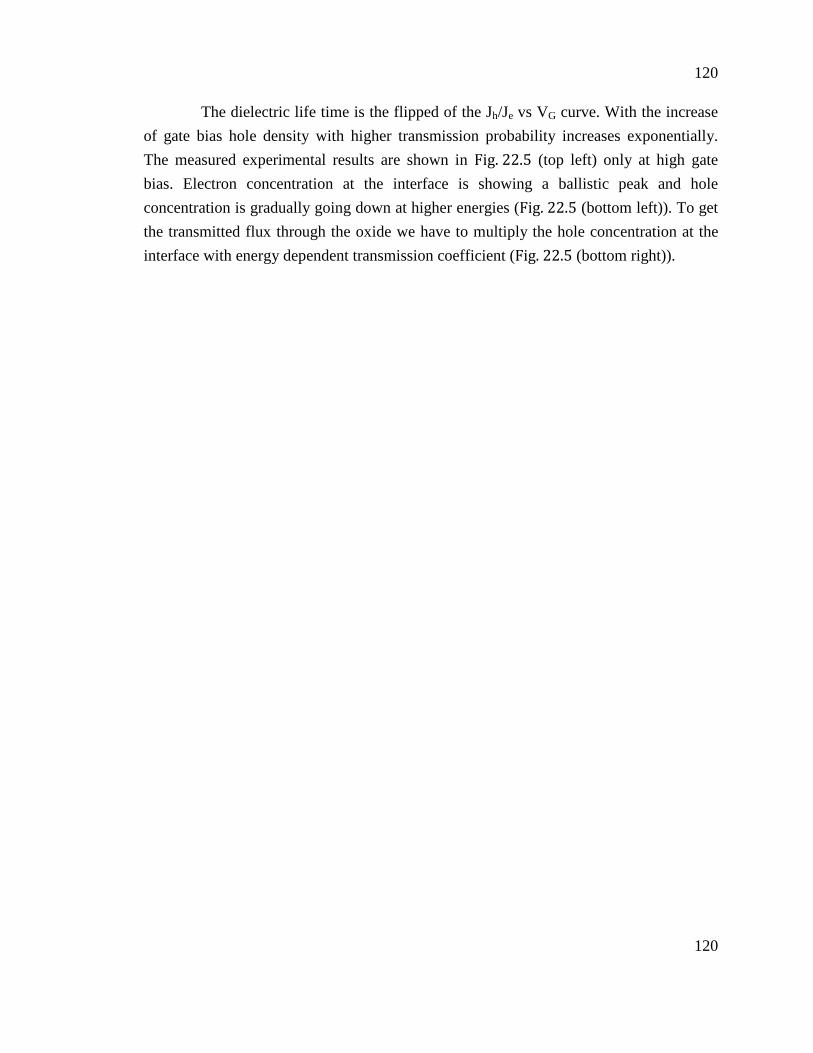
The dielectric life time is the flipped of the Jh/Je vs VG curve. With the increase
of gate bias hole density with higher transmission probability increases exponentially.
The measured experimental results are shown in Fig. 22.5 (top left) only at high gate
bias. Electron concentration at the interface is showing a ballistic peak and hole
concentration is gradually going down at higher energies (Fig. 22.5 (bottom left)). To get
the transmitted flux through the oxide we have to multiply the hole concentration at the
interface with energy dependent transmission coefficient (Fig. 22.5 (bottom right)).
121
121
Fig. 22.5 (Top left) Jh/Je vs VG plot. (Top right) With the increase of the gate bias
hole density with higher transmission probability increases exponentially. (Bottom
left) Electron and hole flux vs energy. Electron flux is showing a ballistic peak
(indicated by arrow). Hole concentration is gradually going down at higher
energies. (Bottom right) Transmitted hole flux, i.e., generated hole multiplied by
the transmission coefficient vs energy is plotted. Transmission probability of
hole is higher at higher energies.

122
122
22.6 Validation of AHI model with experiment
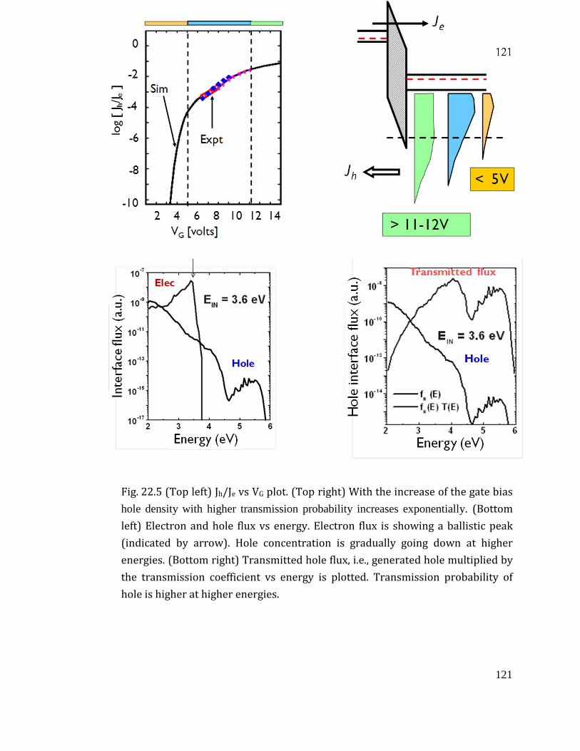
The verification of AHI model is very important because an improper examination of theory might cause an astronomical loss to the industry. Thus we need to verify the theory with experimental data in lots of aspects. According to the anode hole injection model, the determination of oxide time-to-breakdown (TBD) depends on multiple factors such as the oxide thickness and polarity of the oxide barrier. In this section some of these factors that affect TBD are discussed.
22.7 Thickness dependence
One puzzling feature of voltage scaling of TDDB is that for the same oxide
field, thinner oxides have relatively higher projected reliability (higher field acceleration
factor) compared to the thicker oxide (See Error! Reference source not found. (right)) [
22.5]. This suggest us to use parameter other than electric field, could possibly be
voltage, to explain the dielectric lifetime as a function of gate oxide thickness. This
counter-intuitive result can be explained within the framework of AHI model which
requires the lifetime data be plotted as a function of voltage rather than electric field. If
the electric field is fixed across the oxide layers, then the voltage drop across the oxide
has to be lower for the thinner oxide [22.6]. Thus the tunneling electrons do not have so
much energy so they can produce fewer holes. Since the lifetime is inversely proportional
to the hole tunneling current, thinner oxides show better voltage acceleration.
123
123
22.8 Effect of back-gate bias
The application of back-gate bias can influence the oxide time-to-breakdown.
Fig. 22.7 (left top) and (left bottom) below show a PMOS band diagram with two
different conditions: with and without the back-gate bias. As it can be seen from the
figure the larger positive back-gate bias, the more is the acceleration of the injected
electrons and as a result they generate “hotter” holes. This results in higher ionization
(γ66) of carriers in anode and a higher tunneling probability (Tp), and thus the oxide
lifetime is reduced as shown in Fig. 22.7 (right).
Fig. 22.6 For the same electric field (Top left) Schematic band diagram for thin
oxide with low applied bias and (middle) for thick oxide with high bias.
(Right) Dielectric breakdown cannot be explained universally (not scalable)
using field dependent model. Field dependent plot is showing higher
dielectric lifetime for thinner oxide at same lower electric field, which is
anomalous.

124
124
22.9 TBD difference between NMOS and PMOS
The time-to-breakdown also depends on the substrate doping type. Before
comparing TBD of NMOS and PMOS, first let us see the three different types of impact
ionization in the anode. As shown in Fig. 22.8 (bottom), the n-type substrate has majority
carrier impact ionization causing a hole of Energy Einj – EG where Einj is the energy of
injected electrons. For p-type substrate, in addition to the majority carrier ionization
(same as n-type substrate), there is an additional impact ionization called minority carrier
impact ionization. There are two types of minority carrier impact ionization: The hot
electrons can either drop to the conduction band and create a hot hole of energy Einj, or to
the valence band creating a hot hole of energy Einj + EG. The holes left behind deep
Fig. 22.7 The PMOS band diagram for (Left top) no back-gate bias and (left
bottom) positive back-gate bias. (Right) simulated charge-to-breakdown vs VGS
results and corresponding experimental data for different back-gate biases.

125
125
within the valence-band, although few in number, have large kinetic energy and enhanced
tunneling probabilities (See Fig. 22.9). As such, they contribute significantly to the hole
tunneling current.
As explained in Fig. 22.8 (top left), with thin gate oxide and n-type poly
gate there will be majority carrier impact ionization creating low energy holes in anode
(gate). Hole current through gate-oxide will be smaller, so the breakdown. Wherever, for
PMOS with p-type gate with thin gate oxide (Fig. 22.8 (top right)) there will be minority
carrier impact ionization creating highly energetic hole which will see negligible barrier
while flowing through oxide.
Here the availability of minority carrier impact ionization makes the
difference in the oxide time-to-breakdown between NMOS and PMOS (Fig. 22.8). If the
energy of the injected electron from the cathode is Einj, then the maximum energy of the
“hot” hole generated in the anode due to the majority ionization is going to be Einj - EG,
where EG is the silicon band gap (~1.1 eV). This is true for the case of high gate voltage
but the ionization process changes when the applied gate voltage is low.
In case of high gate voltage, the incident energy of the electrons, Einj, is much
larger than the band gap and hence, the hole generation is primarily due to the majority
carriers ionization. Therefore, both PMOS and NMOS have comparable impact
ionization coefficients (αp ~ αn) and hole tunneling probabilities (Tp,p ~ Tp,n) but the
injected electron current is higher in case of NMOS (Je,n > Je,p). Overall, therefore,
NMOS has shorter lifetime than PMOS.

126
126
Fig. 22.8 Schematic band diagram to explain dielectric breakdown mechanism
in (Top left) NMOS and (top right) PMOS. (Bottom) types of impact ionization
including majority and minority carriers.

127
127
For the low voltage case, if the minority carriers are available then the minority
carrier ionization can contribute significantly to the total hole tunneling current. In the
case of PMOS, due to presence of minority carriers at the anode/oxide interface,
additional hole are generated due to two minority carrier ionization mechanisms
discussed in the previous lecture. NMOS does not have free minority carriers. As a result,
PMOS has higher impact ionization and hole tunneling probability (αp >> αn, Tp,p >> Tp,n)
than the NMOS. Though the injected electron current is lower in case of PMOS (Je,n >
Je,p), the combined effect of higher hole ionization and tunneling probabilities ensures
that the oxide breakdown time is shorter in case of PMOS.
22.10 Polarity of gate bias dependence
Fig. 22.10 shows how the AHI model reproduces the polarity gap between gate
and substrate injection. In case of negative gate bias electron current flow direction will
be opposite to the positive gate bias. Since the substrate is p-type for NMOS, there will
Fig. 22.9 Hole generation probabilities with minority carrier impact ionization.
The probabilities for minority carrier impact ionization (sharp peaks at the
right corner) are very small but the corresponding holes are very hot.

128
128
be minority carrier impact ionization with negative gate bias which was unlikely for
positive bias case. As we learnt before that minority carrier impact ionization creates
highly energetic holes with higher transmission probability therefore more destructive.
Dielectric lifetime goes down significantly with negative gate bias for NMOS.
22.11 Voltage scaling and universal shape of TBD
The AHI model requires that TBD be plotted as a function of gate voltage, not as
a function of oxide field. For very high fields, where impact ionization is a weak function
of the electron injection energy, the two procedures are equivalent, because the hole
Fig. 22.10 Positive and negative gate bias dependence of the dielectric lifetime.
Band diagram (top left) at positive gate bias, (bottom left) at negative gate bias,
and (right) lifetime vs oxide electric field at positive and negative gate biases.
Because of minority carrier impact ionization life time goes down at negative gate
bias.

129
129
current is primarily determined by electron and hole tunneling components which can be
plotted against voltage or oxide field equally well. However, at lower voltages for thinner
oxides, the injection energy for electrons becomes critically important in determining the
impact ionization efficiency of the injected electrons. Since the injection energy is
directly related to the voltage, plotting TBD against voltage becomes appropriate for
thinner oxides. Therefore, we plot the simulation results for 4 and 7 nm oxides, discussed
in Error! Reference source not found., as a function of voltage in Fig. 22.11.
Interestingly, when scaled vertically with respect to each other (see Fig. 22.11), the TBD
vs. V curve does show a “universal” shape since the two contributing processes - the
tunneling current and the impact ionization, have specific voltage dependent variations.
This scaling of the “y-axis” by a constant factor accounts for the difference in critical trap
densities for different oxide thicknesses (i.e., TBD = NBD/R, R is the trap generation rate),
so that the shape of the shifted profile reflects the voltage dependence of trap generation
process. The field acceleration factor (γ66) of this particular “universal” curve as a
function of V (see Error! Reference source not found. (right)) does indicate the
possibility of improved voltage acceleration factor as gate voltage is reduced.
Fig. 22.11 (Top left) The simulation results shown in Error! Reference source not
found. (right) are re-plotted as a function of gate voltage. (Bottom left) If two
curves are scaled (“y-axis” only) with respect to each other, they show a
“universal” curve as a function of gate voltage. (Right) Few more results are

130
130
22.12 Conclusion:
The Anode-Hole Injection (AHI) model provides the theoretical framework for
understanding the time-dependent dielectric breakdown (TDDB) phenomena. The role of
hot holes in creating defects inside the gate dielectric implies that dielectric breakdown is
a voltage-driven process rather than a field-driven process because the low voltage hole
generation process is dominated by the efficiency of impact ionization process which is a
strong function of gate voltage. The universality of time-to-breakdown with respect to
gate voltage also validates that it is a voltage-driven process. AHI model also shows that
PMOS and NMOS have different voltage scaling relationship due to the availability of
minority carrier in the anode.
22.13 References
[22.1] M. A. Alam, Bonnie E. Weir, and P. Silverman, “A Future of Function or
Failure?,” IEEE Circuits and Devices - The Electronics and Photonics Magazine
18(2), pp. 42-48, 2002.
[22.2] B. Weir, C. Leung, P. Silverman, and M. Alam, “Gate Dielectric Breakdown in the
Time-Scale of ESD Breakdown,” Microelectronics Reliability, 45, pp. 427-436,
2005.
[22.3] B. E. Weir, C.-C. Leung, P. J. Silverman, and M. Alam, “Gate dielectric
breakdown: a focus on ESD protection,” Proc. of IRPS, pp. 399-404, 2004.
[22.4] A. Ghetti, M. A. Alam, and J. Bude, “Anode Hole Generation Mechanisms,”
Microelectronics Reliability, 41(9), pp. 1347-1354, 2001.
[22.5] M. A. Alam, Jeff Bude, and A. Ghetti, “Can an Accurate Anode Hole Injection
Model Resolve the E vs. 1/E controversy?,” Proceedings of International
Reliability Physics Symposium, pp. 21-26, (2000).
[22.6] M. A. Alam, R. K. Smith, B. E. Weir, and P. J. Silverman, “Uncorrelated
Breakdown of Silicon Integrated Circuits,” Nature, 6914, p. 378, 2002.

131
131
[22.7] M. Alam and R. K. Smith, “A Phenomenological Theory of Correlated Multiple
Soft Breakdown Events in Ultrathin Gate Dielectrics, ” Proc. of International
Reliability Physics Symposium, pp. 406-411, 2003.
[22.8] M. A. Alam, B. E. Weir, and P. J. Silverman, “A study of soft and hard
breakdown-Part I: Analysis of statistical percolation conductance,” IEEE
Transaction on Electron Devices, 49 (2), pp. 232-238, 2002.
[22.9] M. A. Alam, B. E. Weir, and P. J. Silverman, “A study of soft and hard
breakdown-Part II: Principles of area, thickness, and voltage scaling,” IEEE
Transaction on Electron Devices, 49 (2), pp. 239-246, 2002.
[22.10] B. E. Weir, M. A. Alam, J. D. Bude, P. J. Silverman, A. Ghetti, F. Baumann, P.
Diodato et al. "Gate oxide reliability projection to the sub-2 nm regime."
Semiconductor Science and Technology 15 (5), p. 455, 2000.
[22.11] Ben Kaczer, Robin Degraeve, Nadège Pangon, Tanya Nigam, and Guido
Groeseneken. "Investigation of temperature acceleration of thin oxide time-to-
breakdown." Microelectronic engineering 48 (1), pp. 47-50, 1999.
[22.12] J. S. Suehle , E. M. Vogel , B. Wang and J. B. Bernstein "Temperature
Dependence of Soft Breakdown and Wear-Out in Sub-3 nm SiO2 Films", Proc.
IRPS, pp.33 -39, 2000.
[22.13] M. A. Alam, “SILC as a Measure of Trap Generation and Predictor of TBD in
Ultrathin Oxides,” IEEE Transaction on Electron Devices, 49 (2), pp. 226-231,
2002.
[22.14] M. Alam, D. Monroe, B. Weir, and P. Silverman, “Theory of Current-Ratio
Method for Oxide Reliability: Proposal and Validation of a New Class of Two-
Dimensional Breakdown-Spot Characterization Techniques,” Proceedings of
International Electron Device Meeting, 2005.