Tutorial III: Nios II Processor Software Developmentlawford/3TB4/ref/nios2-1.pdf · Tutorial III:...
29
The Nios II IDE tool compiles C/C++ code for the Nios II processor and provides an integrated software development environment for Nios II systems. CHAPTER 16 Tutorial III: Nios II Processor Software Development
Transcript of Tutorial III: Nios II Processor Software Developmentlawford/3TB4/ref/nios2-1.pdf · Tutorial III:...
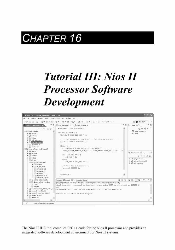
The Nios II IDE tool compiles C/C++ code for the Nios II processor and provides an integrated software development environment for Nios II systems.
CHAPTER 16
Tutorial III: Nios II Processor Software Development
322 Rapid Prototyping of Digital Systems Chapter 16
16 Tutorial III: Nios II Processor Software Development Designing systems with embeddeded processors requires both hardware and software design elements. A collection of CAD tools developed by Altera enable you to design both the hardware and software for a fully functional, customizable, soft-core processor called Nios II. This tutorial steps you through the software development for a Nios II processor executing on the DE board. A Nios II processor reference design targeted for the DE board is used here. To design a custom Nios II processor refer to Tutorial IV (in the following chapter), which introduces the hardware design tools for the Nios II processor.
Upon completion of this tutorial, you will be able to: • Navigate Altera’s Nios II Integrated Development Environment (IDE), • Write a C-language software program that executes on the Nios II
reference design, • Download and execute a software program on the Nios II processor, and • Test the peripherals and memory components of the Nios II reference
design on a DE1 or DE2 board. This tutorial will step you through writing and running two programs for the Nios II processor. First, a simple “Hello World” type of program will be written, compiled, downloaded to the DE board, and run. Next, a test program that uses interrupts, pushbuttons, switches, LEDs, SRAM, Flash memory, SDRAM, and the LCD display (on the DE2 board only) will be written that can be used to test the major peripherals on the DE board.
THE DVD CONTAINS A VERSION OF CHAPTERS 16 AND 17 FOR THE
UP 3 BOARDS.
16.1 Install the DE board files Run the installation program for Altera’s University Program IP Library. This program can be found on the DVD at \Altera_Software\UP_IP_Library.exe.
16.2 Starting a Nios II Software Project The Nios II Integrated Development Environment (IDE) is a standalone program that works in conjunction with Quartus II. To design software in the IDE, Quartus II does not have to be installed on your system; however, you will need a valid Quartus II project with a Nios II processor in it to use the IDE. A Nios II reference design for the DE board is included on the DVD that came with this book. This hardware design will be used for the remainder of this tutorial. Copy the design files from booksoft_fe\de2\chap16 on the DVD to a working directory on your hard drive. (If you are using a DE1 board, then copy the files from the booksoft_fe\de1\chap16 folder on the DVD.) The software design files will be stored in a subdirectory of this project directory.
Tutorial III: Nios II Processor Software Development 323
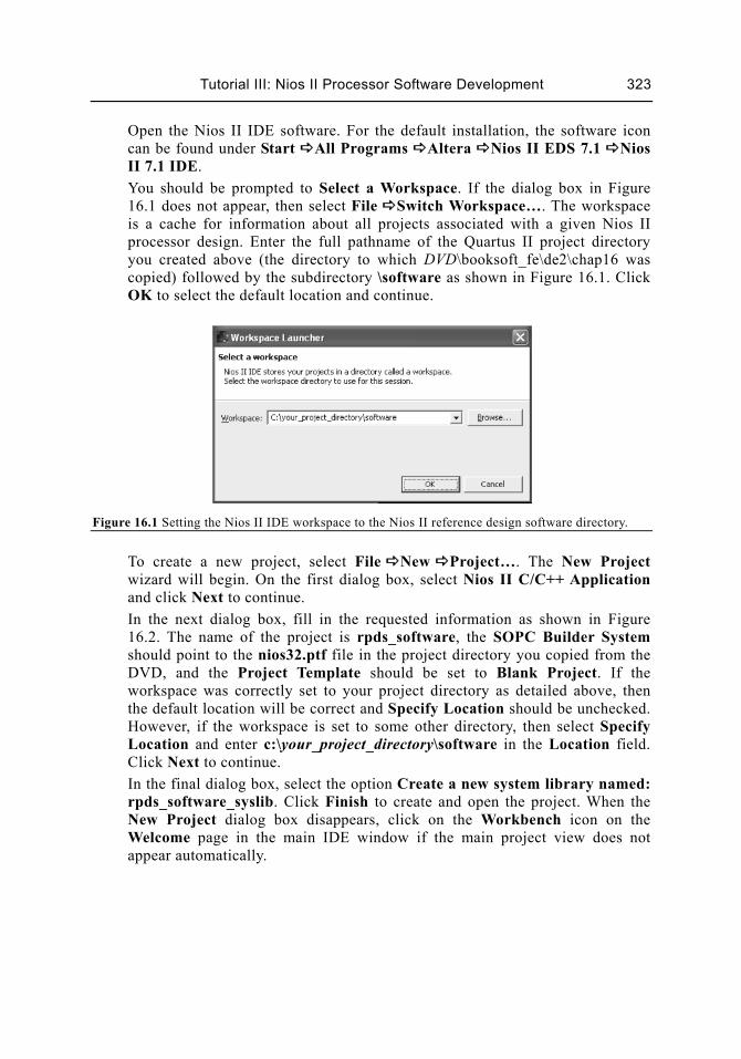
Open the Nios II IDE software. For the default installation, the software icon can be found under Start All Programs Altera Nios II EDS 7.1 Nios II 7.1 IDE. You should be prompted to Select a Workspace. If the dialog box in Figure 16.1 does not appear, then select File Switch Workspace…. The workspace is a cache for information about all projects associated with a given Nios II processor design. Enter the full pathname of the Quartus II project directory you created above (the directory to which DVD\booksoft_fe\de2\chap16 was copied) followed by the subdirectory \software as shown in Figure 16.1. Click OK to select the default location and continue.
Figure 16.1 Setting the Nios II IDE workspace to the Nios II reference design software directory.
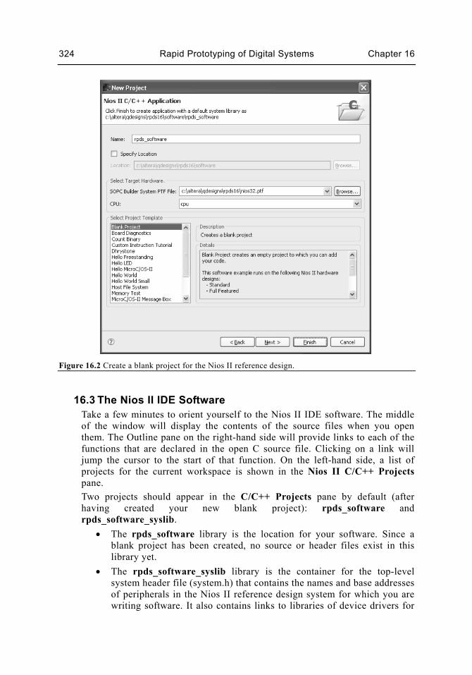
To create a new project, select File New Project…. The New Project wizard will begin. On the first dialog box, select Nios II C/C++ Application and click Next to continue. In the next dialog box, fill in the requested information as shown in Figure 16.2. The name of the project is rpds_software, the SOPC Builder System should point to the nios32.ptf file in the project directory you copied from the DVD, and the Project Template should be set to Blank Project. If the workspace was correctly set to your project directory as detailed above, then the default location will be correct and Specify Location should be unchecked. However, if the workspace is set to some other directory, then select Specify Location and enter c:\your_project_directory\software in the Location field. Click Next to continue. In the final dialog box, select the option Create a new system library named: rpds_software_syslib. Click Finish to create and open the project. When the New Project dialog box disappears, click on the Workbench icon on the Welcome page in the main IDE window if the main project view does not appear automatically.
324 Rapid Prototyping of Digital Systems Chapter 16
Figure 16.2 Create a blank project for the Nios II reference design.
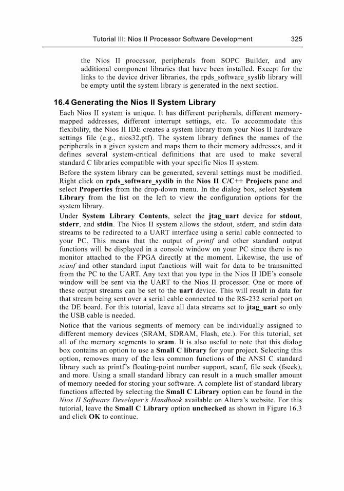
16.3 The Nios II IDE Software Take a few minutes to orient yourself to the Nios II IDE software. The middle of the window will display the contents of the source files when you open them. The Outline pane on the right-hand side will provide links to each of the functions that are declared in the open C source file. Clicking on a link will jump the cursor to the start of that function. On the left-hand side, a list of projects for the current workspace is shown in the Nios II C/C++ Projects pane. Two projects should appear in the C/C++ Projects pane by default (after having created your new blank project): rpds_software and rpds_software_syslib.
• The rpds_software library is the location for your software. Since a blank project has been created, no source or header files exist in this library yet.
• The rpds_software_syslib library is the container for the top-level system header file (system.h) that contains the names and base addresses of peripherals in the Nios II reference design system for which you are writing software. It also contains links to libraries of device drivers for
Tutorial III: Nios II Processor Software Development 325
the Nios II processor, peripherals from SOPC Builder, and any additional component libraries that have been installed. Except for the links to the device driver libraries, the rpds_software_syslib library will be empty until the system library is generated in the next section.
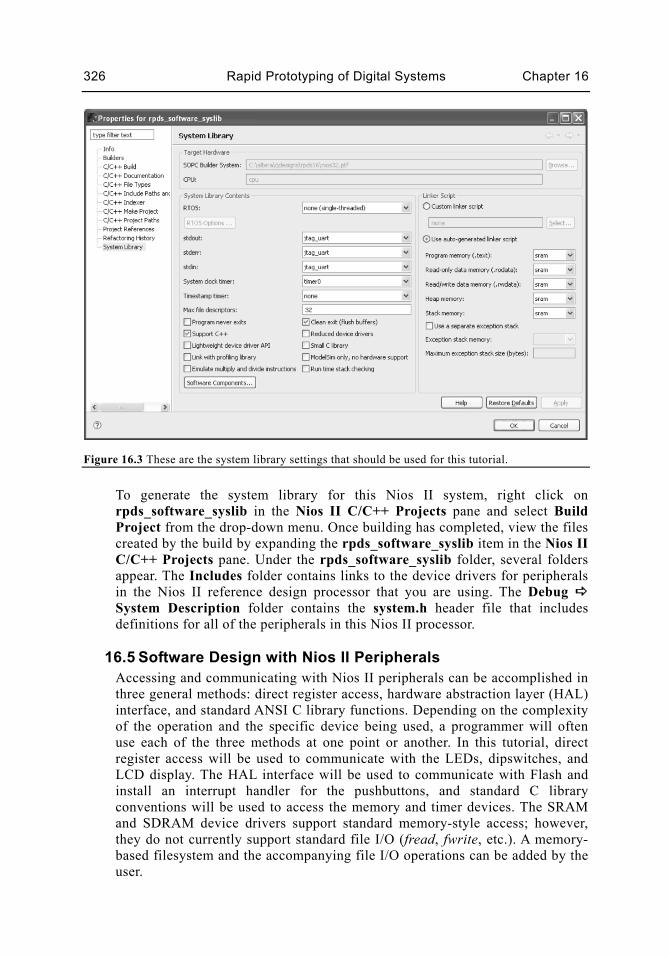
16.4 Generating the Nios II System Library Each Nios II system is unique. It has different peripherals, different memory-mapped addresses, different interrupt settings, etc. To accommodate this flexibility, the Nios II IDE creates a system library from your Nios II hardware settings file (e.g., nios32.ptf). The system library defines the names of the peripherals in a given system and maps them to their memory addresses, and it defines several system-critical definitions that are used to make several standard C libraries compatible with your specific Nios II system. Before the system library can be generated, several settings must be modified. Right click on rpds_software_syslib in the Nios II C/C++ Projects pane and select Properties from the drop-down menu. In the dialog box, select System Library from the list on the left to view the configuration options for the system library. Under System Library Contents, select the jtag_uart device for stdout, stderr, and stdin. The Nios II system allows the stdout, stderr, and stdin data streams to be redirected to a UART interface using a serial cable connected to your PC. This means that the output of printf and other standard output functions will be displayed in a console window on your PC since there is no monitor attached to the FPGA directly at the moment. Likewise, the use of scanf and other standard input functions will wait for data to be transmitted from the PC to the UART. Any text that you type in the Nios II IDE’s console window will be sent via the UART to the Nios II processor. One or more of these output streams can be set to the uart device. This will result in data for that stream being sent over a serial cable connected to the RS-232 serial port on the DE board. For this tutorial, leave all data streams set to jtag_uart so only the USB cable is needed. Notice that the various segments of memory can be individually assigned to different memory devices (SRAM, SDRAM, Flash, etc.). For this tutorial, set all of the memory segments to sram. It is also useful to note that this dialog box contains an option to use a Small C library for your project. Selecting this option, removes many of the less common functions of the ANSI C standard library such as printf’s floating-point number support, scanf, file seek (fseek), and more. Using a small standard library can result in a much smaller amount of memory needed for storing your software. A complete list of standard library functions affected by selecting the Small C Library option can be found in the Nios II Software Developer’s Handbook available on Altera’s website. For this tutorial, leave the Small C Library option unchecked as shown in Figure 16.3 and click OK to continue.
326 Rapid Prototyping of Digital Systems Chapter 16
Figure 16.3 These are the system library settings that should be used for this tutorial.
To generate the system library for this Nios II system, right click on rpds_software_syslib in the Nios II C/C++ Projects pane and select Build Project from the drop-down menu. Once building has completed, view the files created by the build by expanding the rpds_software_syslib item in the Nios II C/C++ Projects pane. Under the rpds_software_syslib folder, several folders appear. The Includes folder contains links to the device drivers for peripherals in the Nios II reference design processor that you are using. The Debug System Description folder contains the system.h header file that includes definitions for all of the peripherals in this Nios II processor.
16.5 Software Design with Nios II Peripherals Accessing and communicating with Nios II peripherals can be accomplished in three general methods: direct register access, hardware abstraction layer (HAL) interface, and standard ANSI C library functions. Depending on the complexity of the operation and the specific device being used, a programmer will often use each of the three methods at one point or another. In this tutorial, direct register access will be used to communicate with the LEDs, dipswitches, and LCD display. The HAL interface will be used to communicate with Flash and install an interrupt handler for the pushbuttons, and standard C library conventions will be used to access the memory and timer devices. The SRAM and SDRAM device drivers support standard memory-style access; however, they do not currently support standard file I/O (fread, fwrite, etc.). A memory-based filesystem and the accompanying file I/O operations can be added by the user.
Tutorial III: Nios II Processor Software Development 327
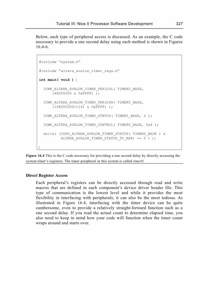
Below, each type of peripheral access is discussed. As an example, the C code necessary to provide a one second delay using each method is shown in Figures 16.4-6.
#include “system.h” #include “altera_avalon_timer_regs.h” int main( void ) { IOWR_ALTERA_AVALON_TIMER_PERIODL( TIMER0_BASE,
(48000000 & 0xFFFF) ); IOWR_ALTERA_AVALON_TIMER_PERIODH( TIMER0_BASE,
((48000000>>16) & 0xFFFF) ); IOWR_ALTERA_AVALON_TIMER_STATUS( TIMER0_BASE, 0 ); IOWR_ALTERA_AVALON_TIMER_CONTROL( TIMER0_BASE, 0x4 ); while( (IORD_ALTERA_AVALON_TIMER_STATUS( TIMER0_BASE ) & ALTERA_AVALON_TIMER_STATUS_TO_MSK) == 0 ) {} }
Figure 16.4 This is the C code necessary for providing a one second delay by directly accessing the system timer’s registers. The timer peripheral in this system is called timer0.
Direct Register Access
Each peripheral’s registers can be directly accessed through read and write macros that are defined in each component’s device driver header file. This type of communication is the lowest level and while it provides the most flexibility in interfacing with peripherals, it can also be the most tedious. As illustrated in Figure 16.4, interfacing with the timer device can be quite cumbersome, even to provide a relatively straight-forward function such as a one second delay. If you read the actual count to determine elapsed time, you also need to keep in mind how your code will function when the timer count wraps around and starts over.
328 Rapid Prototyping of Digital Systems Chapter 16
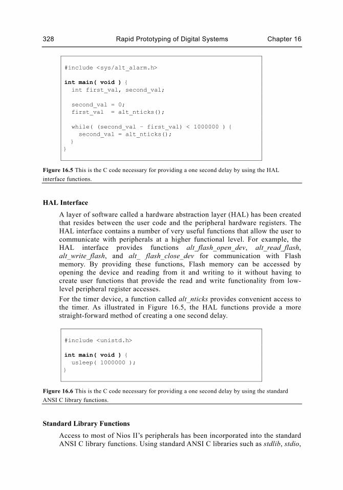
#include <sys/alt_alarm.h> int main( void ) { int first_val, second_val; second_val = 0; first_val = alt_nticks(); while( (second_val – first_val) < 1000000 ) { second_val = alt_nticks(); } }
Figure 16.5 This is the C code necessary for providing a one second delay by using the HAL interface functions.
HAL Interface
A layer of software called a hardware abstraction layer (HAL) has been created that resides between the user code and the peripheral hardware registers. The HAL interface contains a number of very useful functions that allow the user to communicate with peripherals at a higher functional level. For example, the HAL interface provides functions alt_flash_open_dev, alt_read_flash, alt_write_flash, and alt_ flash_close_dev for communication with Flash memory. By providing these functions, Flash memory can be accessed by opening the device and reading from it and writing to it without having to create user functions that provide the read and write functionality from low-level peripheral register accesses. For the timer device, a function called alt_nticks provides convenient access to the timer. As illustrated in Figure 16.5, the HAL functions provide a more straight-forward method of creating a one second delay.
#include <unistd.h> int main( void ) { usleep( 1000000 ); }
Figure 16.6 This is the C code necessary for providing a one second delay by using the standard ANSI C library functions.
Standard Library Functions
Access to most of Nios II’s peripherals has been incorporated into the standard ANSI C library functions. Using standard ANSI C libraries such as stdlib, stdio,

Tutorial III: Nios II Processor Software Development 329
string, time, malloc, etc. you can manipulate strings, access memory and memory-like devices through standard file I/O functions, use the timer to add a delay using usleep or wait functions, and much more. This is the highest level of abstraction provided by the Nios II IDE. Many of these functions use the peripheral-specific HAL functions to provide a single common interface to various types of peripherals. For example, fopen, fread, fwrite, and fclose functions from the stdio library can be used for memory accesses on some SDRAM, Flash, or SRAM memory devices. The system library functions will use the appropriate HAL function calls for each access depending on the particular memory device being used. To create a one second delay using the timer, a single call to the standard library function usleep can be made as shown in Figure 16.6
#ifndef _RPDS_SOFTWARE_H_ #define _RPDS_SOFTWARE_H_ #include <stdio.h> #include <unistd.h> #include "system.h" #include "altera_avalon_pio_regs.h" #endif //_RPDS_SOFTWARE_H_
Figure 16.7 This is your first C program’s main header file.
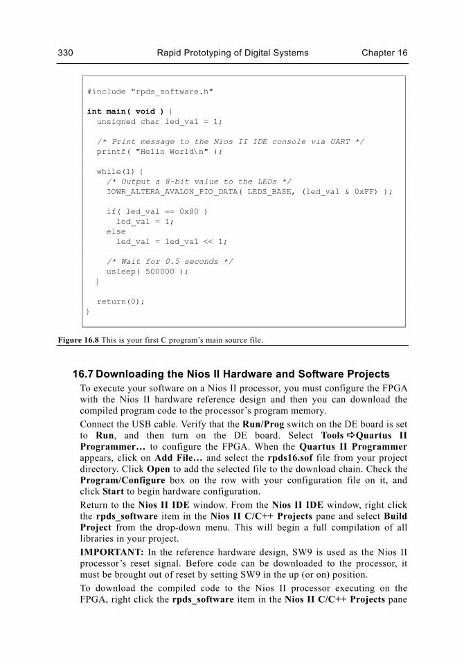
16.6 Starting Software Design – main() Create a C header file by selecting the rpds_software item in the Nios II C/C++ Projects pane. Choose File New Header File. When the dialog box appears, enter rpds_software.h for the Header File and click Finish to continue. Start your program’s main header file by adding the #include and definition statements shown in Figure 16.7. The C program that you will now write will print “Hello World” in the Nios II IDE’s console window (via the UART and serial cable), and it will blink eight of the red LEDs on the DE board. Create your program’s main C source file by selecting the rpds_software item in the Nios II C/C++ Projects pane. Choose File New File. When the dialog box appears, enter rpds_software.c for the File name and click Finish to continue. Start your program by including the rpds_software.h header file and typing the code shown in Figure 16.8.
330 Rapid Prototyping of Digital Systems Chapter 16
#include "rpds_software.h" int main( void ) { unsigned char led_val = 1; /* Print message to the Nios II IDE console via UART */ printf( "Hello World\n" ); while(1) { /* Output a 8-bit value to the LEDs */ IOWR_ALTERA_AVALON_PIO_DATA( LEDS_BASE, (led_val & 0xFF) ); if( led_val == 0x80 ) led_val = 1; else led_val = led_val << 1; /* Wait for 0.5 seconds */ usleep( 500000 ); } return(0); }
Figure 16.8 This is your first C program’s main source file.
16.7 Downloading the Nios II Hardware and Software Projects To execute your software on a Nios II processor, you must configure the FPGA with the Nios II hardware reference design and then you can download the compiled program code to the processor’s program memory. Connect the USB cable. Verify that the Run/Prog switch on the DE board is set to Run, and then turn on the DE board. Select Tools Quartus II Programmer… to configure the FPGA. When the Quartus II Programmer appears, click on Add File… and select the rpds16.sof file from your project directory. Click Open to add the selected file to the download chain. Check the Program/Configure box on the row with your configuration file on it, and click Start to begin hardware configuration. Return to the Nios II IDE window. From the Nios II IDE window, right click the rpds_software item in the Nios II C/C++ Projects pane and select Build Project from the drop-down menu. This will begin a full compilation of all libraries in your project. IMPORTANT: In the reference hardware design, SW9 is used as the Nios II processor’s reset signal. Before code can be downloaded to the processor, it must be brought out of reset by setting SW9 in the up (or on) position. To download the compiled code to the Nios II processor executing on the FPGA, right click the rpds_software item in the Nios II C/C++ Projects pane
Tutorial III: Nios II Processor Software Development 331
and select Run As Nios II Hardware. If the run settings dialog box appears, click the Run button to close this box. If the run settings dialog box appears, click the Run button to close this box.
16.8 Executing the Software Once the program code has been downloaded to the Nios II processor’s program memory (SRAM in this configuration), your code automatically begins executing. As a part of the normal download process, the Nios II IDE downloads your program to memory and then reads the program memory back to verify that the code in program memory is correct. If there are any problems with downloading your program, then the processor is stalled and a message that alerts you to this fact appears in the Console pane in the bottom right-hand side of the Nios II IDE window. If this happens, verify that SW9 is in the up (on) position and then right click the rpds_software item in the Nios II C/C++ Projects pane and select Run As Nios II Hardware again. Once your program begins executing, the Nios II IDE’s Console pane becomes a standard input/output terminal connected to your processor via the RS-232 UART device and cable. The text message “Hello World” should appear in the Console pane as soon as your program begins. Also, eight of the red LEDs on the DE board should blink one at a time.
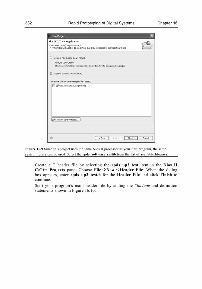
16.9 Starting Software Design for a Peripheral Test Program Now that you have written your first program and have it successfully running on the DE board, it is time to write a longer program that will test each of the major peripheral components on the DE board. A second project can be added to the current workspace, and since the same Nios II processor is being used for all projects in this workspace, the same system library can be used for them all. This option will be selected in the dialog box shown in Figure 16.9. To create a new project, select File New Project…. The New Project wizard will begin. On the first dialog box, select Nios II C/C++ Application and click Next to continue. In the next dialog box, fill in the requested information. The name of the project is rpds_de_test, the SOPC Builder System should point to the nios32.ptf file in your hardware project directory, and the Project Template should be set to Blank Project. If the workspace was correctly set to your project directory as detailed above, then the default location will be correct and Specify Location should be unchecked. However, if the workspace is set to some other directory, then select Specify Location and enter c:\your_project_directory\software in the Location field. Click Next to continue. In the final dialog box, select the option Select or create a system library and choose the rpds_software_syslib project from the list of Available System Library Projects for: nios32 as shown in Figure 16.9. Click Finish to create and open the project.
332 Rapid Prototyping of Digital Systems Chapter 16
Figure 16.9 Since this project uses the same Nios II processor as your first program, the same system library can be used. Select the rpds_software_syslib from the list of available libraries.
Create a C header file by selecting the rpds_up3_test item in the Nios II C/C++ Projects pane. Choose File New Header File. When the dialog box appears, enter rpds_up3_test.h for the Header File and click Finish to continue. Start your program’s main header file by adding the #include and definition statements shown in Figure 16.10.
Tutorial III: Nios II Processor Software Development 333
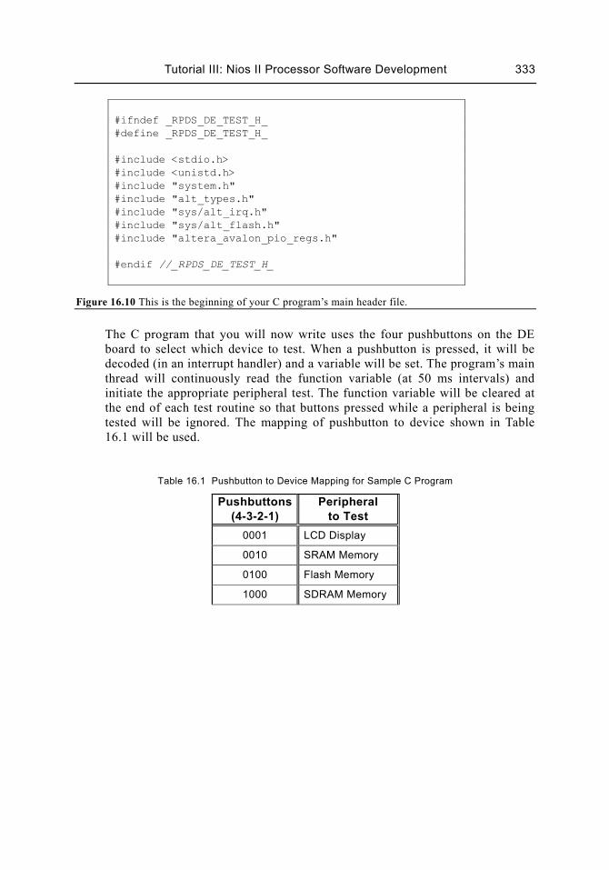
#ifndef _RPDS_DE_TEST_H_ #define _RPDS_DE_TEST_H_ #include <stdio.h> #include <unistd.h> #include "system.h" #include "alt_types.h" #include "sys/alt_irq.h" #include "sys/alt_flash.h" #include "altera_avalon_pio_regs.h" #endif //_RPDS_DE_TEST_H_
Figure 16.10 This is the beginning of your C program’s main header file.
The C program that you will now write uses the four pushbuttons on the DE board to select which device to test. When a pushbutton is pressed, it will be decoded (in an interrupt handler) and a variable will be set. The program’s main thread will continuously read the function variable (at 50 ms intervals) and initiate the appropriate peripheral test. The function variable will be cleared at the end of each test routine so that buttons pressed while a peripheral is being tested will be ignored. The mapping of pushbutton to device shown in Table 16.1 will be used.
Table 16.1 Pushbutton to Device Mapping for Sample C Program
Pushbuttons(4-3-2-1)
Peripheral to Test
0001 LCD Display
0010 SRAM Memory
0100 Flash Memory
1000 SDRAM Memory
334 Rapid Prototyping of Digital Systems Chapter 16
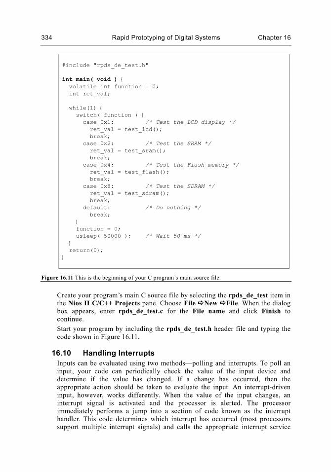
#include "rpds_de_test.h" int main( void ) { volatile int function = 0; int ret_val; while(1) { switch( function ) { case 0x1: /* Test the LCD display */ ret_val = test_lcd(); break; case 0x2: /* Test the SRAM */ ret_val = test_sram(); break; case 0x4: /* Test the Flash memory */ ret_val = test_flash(); break; case 0x8: /* Test the SDRAM */ ret_val = test_sdram(); break; default: /* Do nothing */ break; } function = 0; usleep( 50000 ); /* Wait 50 ms */ } return(0); }
Figure 16.11 This is the beginning of your C program’s main source file.
Create your program’s main C source file by selecting the rpds_de_test item in the Nios II C/C++ Projects pane. Choose File New File. When the dialog box appears, enter rpds_de_test.c for the File name and click Finish to continue. Start your program by including the rpds_de_test.h header file and typing the code shown in Figure 16.11.
16.10 Handling Interrupts Inputs can be evaluated using two methods—polling and interrupts. To poll an input, your code can periodically check the value of the input device and determine if the value has changed. If a change has occurred, then the appropriate action should be taken to evaluate the input. An interrupt-driven input, however, works differently. When the value of the input changes, an interrupt signal is activated and the processor is alerted. The processor immediately performs a jump into a section of code known as the interrupt handler. This code determines which interrupt has occurred (most processors support multiple interrupt signals) and calls the appropriate interrupt service
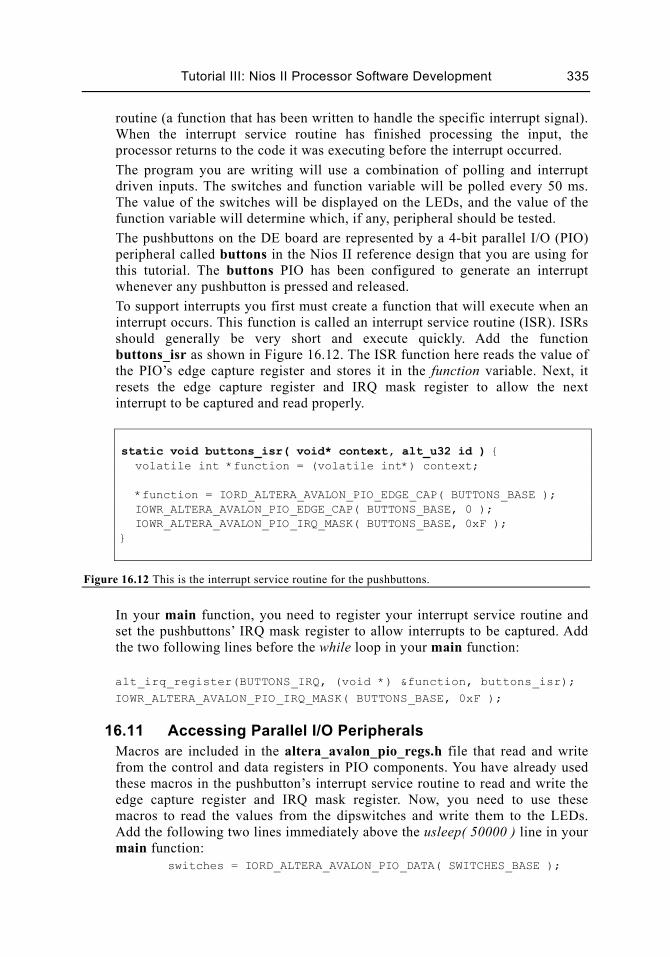
Tutorial III: Nios II Processor Software Development 335
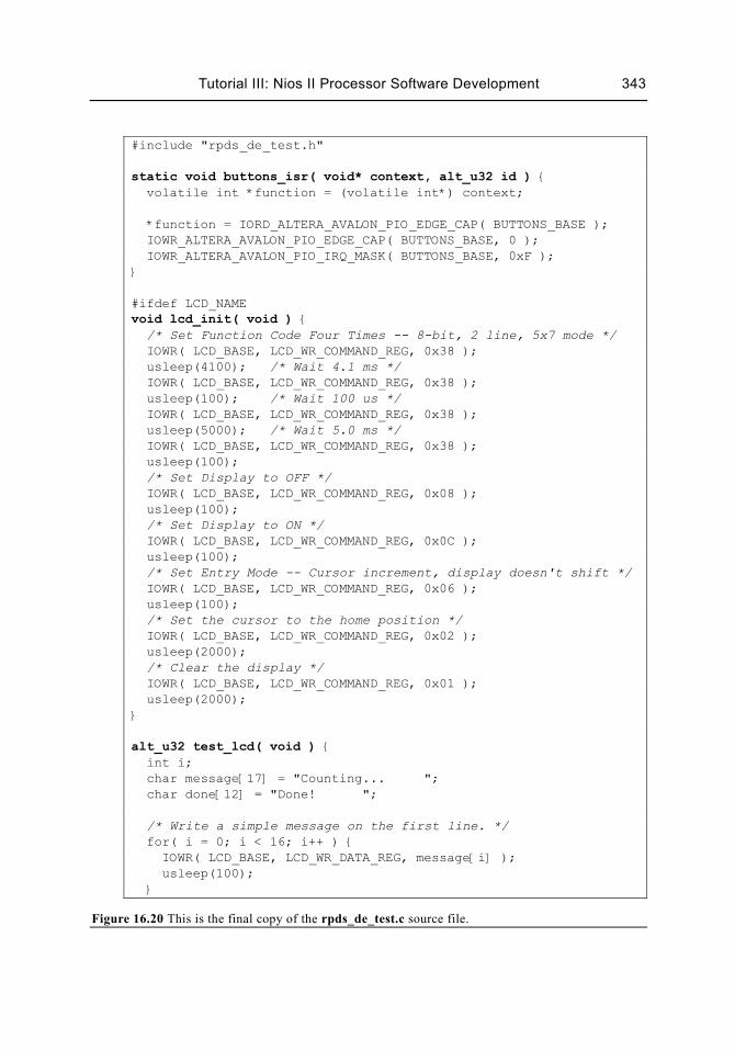
routine (a function that has been written to handle the specific interrupt signal). When the interrupt service routine has finished processing the input, the processor returns to the code it was executing before the interrupt occurred. The program you are writing will use a combination of polling and interrupt driven inputs. The switches and function variable will be polled every 50 ms. The value of the switches will be displayed on the LEDs, and the value of the function variable will determine which, if any, peripheral should be tested. The pushbuttons on the DE board are represented by a 4-bit parallel I/O (PIO) peripheral called buttons in the Nios II reference design that you are using for this tutorial. The buttons PIO has been configured to generate an interrupt whenever any pushbutton is pressed and released. To support interrupts you first must create a function that will execute when an interrupt occurs. This function is called an interrupt service routine (ISR). ISRs should generally be very short and execute quickly. Add the function buttons_isr as shown in Figure 16.12. The ISR function here reads the value of the PIO’s edge capture register and stores it in the function variable. Next, it resets the edge capture register and IRQ mask register to allow the next interrupt to be captured and read properly.
static void buttons_isr( void* context, alt_u32 id ) { volatile int *function = (volatile int*) context; *function = IORD_ALTERA_AVALON_PIO_EDGE_CAP( BUTTONS_BASE ); IOWR_ALTERA_AVALON_PIO_EDGE_CAP( BUTTONS_BASE, 0 ); IOWR_ALTERA_AVALON_PIO_IRQ_MASK( BUTTONS_BASE, 0xF ); }
Figure 16.12 This is the interrupt service routine for the pushbuttons.
In your main function, you need to register your interrupt service routine and set the pushbuttons’ IRQ mask register to allow interrupts to be captured. Add the two following lines before the while loop in your main function: alt_irq_register(BUTTONS_IRQ, (void *) &function, buttons_isr); IOWR_ALTERA_AVALON_PIO_IRQ_MASK( BUTTONS_BASE, 0xF );
16.11 Accessing Parallel I/O Peripherals Macros are included in the altera_avalon_pio_regs.h file that read and write from the control and data registers in PIO components. You have already used these macros in the pushbutton’s interrupt service routine to read and write the edge capture register and IRQ mask register. Now, you need to use these macros to read the values from the dipswitches and write them to the LEDs. Add the following two lines immediately above the usleep( 50000 ) line in your main function:
switches = IORD_ALTERA_AVALON_PIO_DATA( SWITCHES_BASE );
336 Rapid Prototyping of Digital Systems Chapter 16
IOWR_ALTERA_AVALON_PIO_DATA( LEDS_BASE, switches );
You will also need to add a declaration for the integer variable switches to your main function.
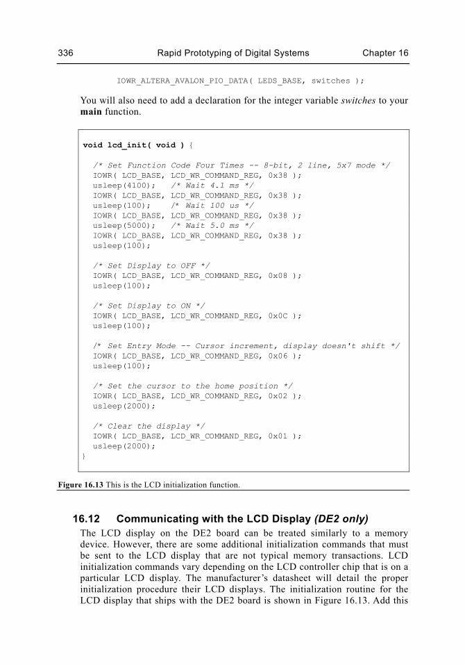
void lcd_init( void ) { /* Set Function Code Four Times -- 8-bit, 2 line, 5x7 mode */ IOWR( LCD_BASE, LCD_WR_COMMAND_REG, 0x38 ); usleep(4100); /* Wait 4.1 ms */ IOWR( LCD_BASE, LCD_WR_COMMAND_REG, 0x38 ); usleep(100); /* Wait 100 us */ IOWR( LCD_BASE, LCD_WR_COMMAND_REG, 0x38 ); usleep(5000); /* Wait 5.0 ms */ IOWR( LCD_BASE, LCD_WR_COMMAND_REG, 0x38 ); usleep(100); /* Set Display to OFF */ IOWR( LCD_BASE, LCD_WR_COMMAND_REG, 0x08 ); usleep(100); /* Set Display to ON */ IOWR( LCD_BASE, LCD_WR_COMMAND_REG, 0x0C ); usleep(100); /* Set Entry Mode -- Cursor increment, display doesn't shift */ IOWR( LCD_BASE, LCD_WR_COMMAND_REG, 0x06 ); usleep(100); /* Set the cursor to the home position */ IOWR( LCD_BASE, LCD_WR_COMMAND_REG, 0x02 ); usleep(2000); /* Clear the display */ IOWR( LCD_BASE, LCD_WR_COMMAND_REG, 0x01 ); usleep(2000); }
Figure 16.13 This is the LCD initialization function.
16.12 Communicating with the LCD Display (DE2 only) The LCD display on the DE2 board can be treated similarly to a memory device. However, there are some additional initialization commands that must be sent to the LCD display that are not typical memory transactions. LCD initialization commands vary depending on the LCD controller chip that is on a particular LCD display. The manufacturer’s datasheet will detail the proper initialization procedure their LCD displays. The initialization routine for the LCD display that ships with the DE2 board is shown in Figure 16.13. Add this
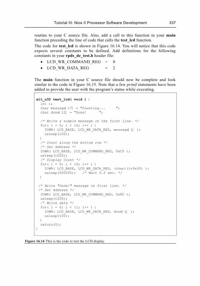
Tutorial III: Nios II Processor Software Development 337
routine to your C source file. Also, add a call to this function in your main function preceding the line of code that calls the test_lcd function. The code for test_lcd is shown in Figure 16.14. You will notice that this code expects several constants to be defined. Add definitions for the following constants in your rpds_de_test.h header file:
• LCD_WR_COMMAND_REG = 0 • LCD_WR_DATA_REG = 2
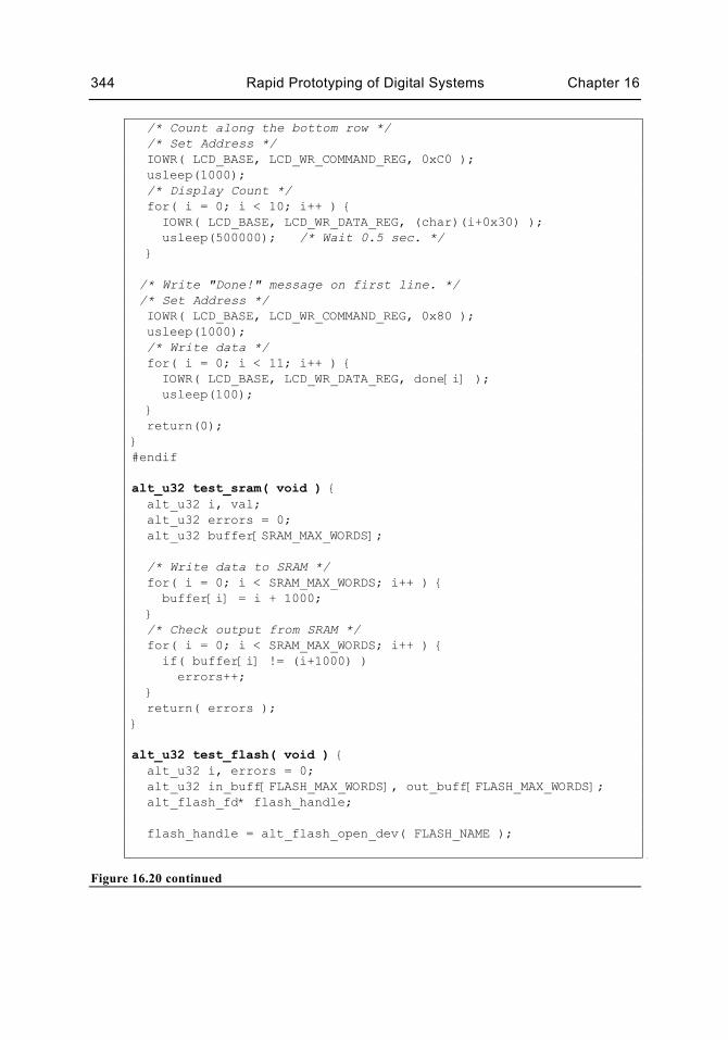
The main function in your C source file should now be complete and look similar to the code in Figure 16.15. Note that a few printf statements have been added to provide the user with the program’s status while executing. alt_u32 test_lcd( void ) { int i; char message[17] = "Counting... "; char done[12] = "Done! "; /* Write a simple message on the first line. */ for( i = 0; i < 16; i++ ) { IOWR( LCD_BASE, LCD_WR_DATA_REG, message[i] ); usleep(100); } /* Count along the bottom row */ /* Set Address */ IOWR( LCD_BASE, LCD_WR_COMMAND_REG, 0xC0 ); usleep(1000); /* Display Count */ for( i = 0; i < 10; i++ ) { IOWR( LCD_BASE, LCD_WR_DATA_REG, (char)(i+0x30) ); usleep(500000); /* Wait 0.5 sec. */ } /* Write "Done!" message on first line. */ /* Set Address */ IOWR( LCD_BASE, LCD_WR_COMMAND_REG, 0x80 ); usleep(1000); /* Write data */ for( i = 0; i < 11; i++ ) { IOWR( LCD_BASE, LCD_WR_DATA_REG, done[i] ); usleep(100); } return(0); }
Figure 16.14 This is the code to test the LCD display.

338 Rapid Prototyping of Digital Systems Chapter 16
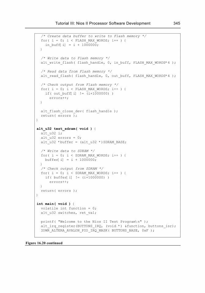
int main( void ) { volatile int function = 0; alt_u32 switches, ret_val; printf("Welcome to the Nios II Test Program\n" ); alt_irq_register(BUTTONS_IRQ, (void *) &function, buttons_isr); IOWR_ALTERA_AVALON_PIO_IRQ_MASK( BUTTONS_BASE, 0xF ); while(1) { switch( function ) { case 0x1: /* Test the LCD display */ printf("Testing LCD Display\n" ); lcd_init(); ret_val = test_lcd(); printf("...Completed.\n" ); break; case 0x2: /* Test the SRAM */ printf("Testing SRAM\n" ); ret_val = test_sram(); printf("...Completed with %d Errors.\n", ret_val ); break; case 0x4: /* Test the Flash memory */ printf("Testing Flash memory\n" ); ret_val = test_flash(); printf("...Completed with %d Errors.\n", ret_val ); break; case 0x8: /* Test the SDRAM */ printf("Testing SDRAM\n" ); ret_val = test_sdram(); printf("...Completed with %d Errors.\n", ret_val ); break; default: /* Do nothing */ break; } function = 0; switches = IORD_ALTERA_AVALON_PIO_DATA( SWITCHES_BASE ); IOWR_ALTERA_AVALON_PIO_DATA( LEDS_BASE, switches ); usleep( 50000 ); } return(0); }
Figure 16.15 This is the completed main function.
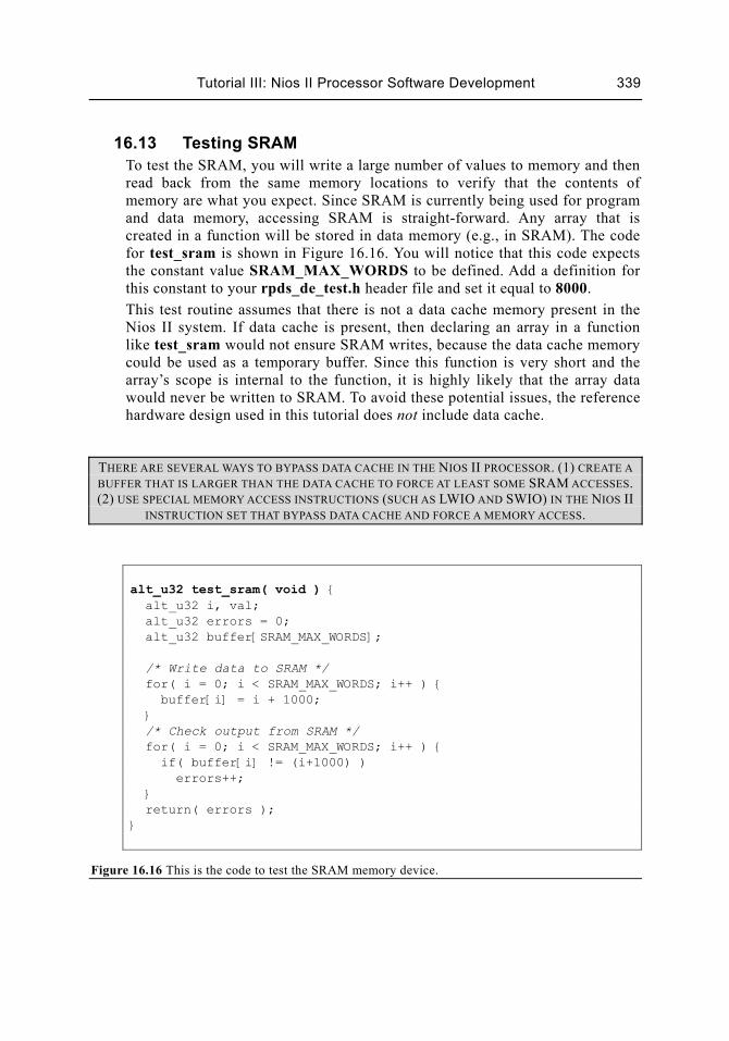
Tutorial III: Nios II Processor Software Development 339
16.13 Testing SRAM To test the SRAM, you will write a large number of values to memory and then read back from the same memory locations to verify that the contents of memory are what you expect. Since SRAM is currently being used for program and data memory, accessing SRAM is straight-forward. Any array that is created in a function will be stored in data memory (e.g., in SRAM). The code for test_sram is shown in Figure 16.16. You will notice that this code expects the constant value SRAM_MAX_WORDS to be defined. Add a definition for this constant to your rpds_de_test.h header file and set it equal to 8000. This test routine assumes that there is not a data cache memory present in the Nios II system. If data cache is present, then declaring an array in a function like test_sram would not ensure SRAM writes, because the data cache memory could be used as a temporary buffer. Since this function is very short and the array’s scope is internal to the function, it is highly likely that the array data would never be written to SRAM. To avoid these potential issues, the reference hardware design used in this tutorial does not include data cache.
THERE ARE SEVERAL WAYS TO BYPASS DATA CACHE IN THE NIOS II PROCESSOR. (1) CREATE A BUFFER THAT IS LARGER THAN THE DATA CACHE TO FORCE AT LEAST SOME SRAM ACCESSES. (2) USE SPECIAL MEMORY ACCESS INSTRUCTIONS (SUCH AS LWIO AND SWIO) IN THE NIOS II
INSTRUCTION SET THAT BYPASS DATA CACHE AND FORCE A MEMORY ACCESS.
alt_u32 test_sram( void ) { alt_u32 i, val; alt_u32 errors = 0; alt_u32 buffer[SRAM_MAX_WORDS]; /* Write data to SRAM */ for( i = 0; i < SRAM_MAX_WORDS; i++ ) { buffer[i] = i + 1000; } /* Check output from SRAM */ for( i = 0; i < SRAM_MAX_WORDS; i++ ) { if( buffer[i] != (i+1000) ) errors++; } return( errors ); }
Figure 16.16 This is the code to test the SRAM memory device.
340 Rapid Prototyping of Digital Systems Chapter 16
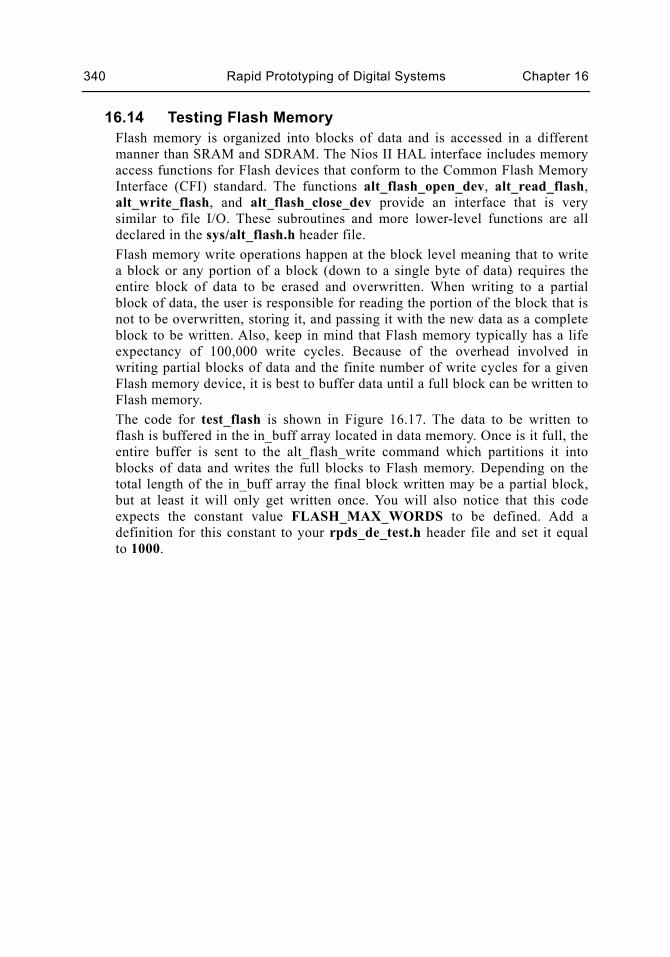
16.14 Testing Flash Memory Flash memory is organized into blocks of data and is accessed in a different manner than SRAM and SDRAM. The Nios II HAL interface includes memory access functions for Flash devices that conform to the Common Flash Memory Interface (CFI) standard. The functions alt_flash_open_dev, alt_read_flash, alt_write_flash, and alt_flash_close_dev provide an interface that is very similar to file I/O. These subroutines and more lower-level functions are all declared in the sys/alt_flash.h header file. Flash memory write operations happen at the block level meaning that to write a block or any portion of a block (down to a single byte of data) requires the entire block of data to be erased and overwritten. When writing to a partial block of data, the user is responsible for reading the portion of the block that is not to be overwritten, storing it, and passing it with the new data as a complete block to be written. Also, keep in mind that Flash memory typically has a life expectancy of 100,000 write cycles. Because of the overhead involved in writing partial blocks of data and the finite number of write cycles for a given Flash memory device, it is best to buffer data until a full block can be written to Flash memory. The code for test_flash is shown in Figure 16.17. The data to be written to flash is buffered in the in_buff array located in data memory. Once is it full, the entire buffer is sent to the alt_flash_write command which partitions it into blocks of data and writes the full blocks to Flash memory. Depending on the total length of the in_buff array the final block written may be a partial block, but at least it will only get written once. You will also notice that this code expects the constant value FLASH_MAX_WORDS to be defined. Add a definition for this constant to your rpds_de_test.h header file and set it equal to 1000.
Tutorial III: Nios II Processor Software Development 341
alt_u32 test_flash( void ) { alt_u32 i, errors = 0; alt_u32 in_buff[FLASH_MAX_WORDS], out_buff[FLASH_MAX_WORDS]; alt_flash_fd* flash_handle; flash_handle = alt_flash_open_dev( FLASH_NAME ); /* Create data buffer to write to Flash memory */ for( i = 0; i < FLASH_MAX_WORDS; i++ ) { in_buff[i] = i + 1000000; } /* Write data to Flash memory */ alt_write_flash( flash_handle, 0, in_buff, FLASH_MAX_WORDS*4 ); /* Read data from Flash memory */ alt_read_flash( flash_handle, 0, out_buff, FLASH_MAX_WORDS*4 ); /* Check output from Flash memory */ for( i = 0; i < FLASH_MAX_WORDS; i++ ) { if( out_buff[i] != (i+1000000) ) errors++; } alt_flash_close_dev( flash_handle ); return( errors ); }
Figure 16.17 This is the code to test the Flash memory device.
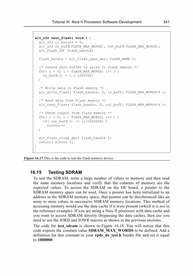
16.15 Testing SDRAM To test the SDRAM, write a large number of values to memory and then read the same memory locations and verify that the contents of memory are the expected values. To access the SDRAM on the DE board, a pointer to the SDRAM memory space can be used. Once a pointer has been initialized to an address in the SDRAM memory space, that pointer can be dereferenced like an array to store values in successive SDRAM memory locations. This method of accessing memory would use the data cache if it were present (which it is not in the reference example). If you are using a Nios II processor with data cache and you want to access SDRAM directly (bypassing the data cache), then use you need to use the IORD and IOWR macros as shown in the previous sections. The code for test_sdram is shown in Figure 16.18. You will notice that this code expects the constant value SDRAM_MAX_WORDS to be defined. Add a definition for this constant to your rpds_de_test.h header file and set it equal to 1000000.
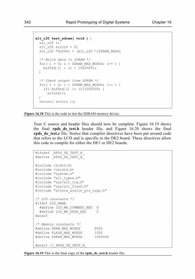
342 Rapid Prototyping of Digital Systems Chapter 16
alt_u32 test_sdram( void ) { alt_u32 i; alt_u32 errors = 0; alt_u32 *buffer = (alt_u32 *)SDRAM_BASE; /* Write data to SDRAM */ for( i = 0; i < SDRAM_MAX_WORDS; i++ ) { buffer[i] = (i + 1000000); } /* Check output from SDRAM */ for( i = 0; i < SDRAM_MAX_WORDS; i++ ) { if( buffer[i] != (i+1000000) ) errors++; } return( errors );}
Figure 16.18 This is the code to test the SDRAM memory device.
Your C source and header files should now be complete. Figure 16.19 shows the final rpds_de_test.h header file, and Figure 16.20 shows the final rpds_de_test.c file. Notice that compiler directives have been put around code that refers to the LCD and is specific to the DE2 board. These directives allow this code to compile for either the DE1 or DE2 boards.
#ifndef _RPDS_DE_TEST_H_ #define _RPDS_DE_TEST_H_ #include <stdio.h> #include <unistd.h> #include "system.h" #include "alt_types.h" #include "sys/alt_irq.h" #include "sys/alt_flash.h" #include "altera_avalon_pio_regs.h" /* LCD constants */ #ifdef LCD_NAME #define LCD_WR_COMMAND_REG 0 #define LCD_WR_DATA_REG 2 #endif /* Memory constants */ #define SRAM_MAX_WORDS 8000 #define FLASH_MAX_WORDS 1000 #define SDRAM_MAX_WORDS 1000000 #endif //_RPDS_DE_TEST_H_
Figure 16.19 This is the final copy of the rpds_de_test.h header file.
Tutorial III: Nios II Processor Software Development 343
#include "rpds_de_test.h" static void buttons_isr( void* context, alt_u32 id ) { volatile int *function = (volatile int*) context; *function = IORD_ALTERA_AVALON_PIO_EDGE_CAP( BUTTONS_BASE ); IOWR_ALTERA_AVALON_PIO_EDGE_CAP( BUTTONS_BASE, 0 ); IOWR_ALTERA_AVALON_PIO_IRQ_MASK( BUTTONS_BASE, 0xF ); } #ifdef LCD_NAME void lcd_init( void ) { /* Set Function Code Four Times -- 8-bit, 2 line, 5x7 mode */ IOWR( LCD_BASE, LCD_WR_COMMAND_REG, 0x38 ); usleep(4100); /* Wait 4.1 ms */ IOWR( LCD_BASE, LCD_WR_COMMAND_REG, 0x38 ); usleep(100); /* Wait 100 us */ IOWR( LCD_BASE, LCD_WR_COMMAND_REG, 0x38 ); usleep(5000); /* Wait 5.0 ms */ IOWR( LCD_BASE, LCD_WR_COMMAND_REG, 0x38 ); usleep(100); /* Set Display to OFF */ IOWR( LCD_BASE, LCD_WR_COMMAND_REG, 0x08 ); usleep(100); /* Set Display to ON */ IOWR( LCD_BASE, LCD_WR_COMMAND_REG, 0x0C ); usleep(100); /* Set Entry Mode -- Cursor increment, display doesn't shift */ IOWR( LCD_BASE, LCD_WR_COMMAND_REG, 0x06 ); usleep(100); /* Set the cursor to the home position */ IOWR( LCD_BASE, LCD_WR_COMMAND_REG, 0x02 ); usleep(2000); /* Clear the display */ IOWR( LCD_BASE, LCD_WR_COMMAND_REG, 0x01 ); usleep(2000); } alt_u32 test_lcd( void ) { int i; char message[17] = "Counting... "; char done[12] = "Done! "; /* Write a simple message on the first line. */ for( i = 0; i < 16; i++ ) { IOWR( LCD_BASE, LCD_WR_DATA_REG, message[i] ); usleep(100); }
Figure 16.20 This is the final copy of the rpds_de_test.c source file.
344 Rapid Prototyping of Digital Systems Chapter 16
/* Count along the bottom row */ /* Set Address */ IOWR( LCD_BASE, LCD_WR_COMMAND_REG, 0xC0 ); usleep(1000); /* Display Count */ for( i = 0; i < 10; i++ ) { IOWR( LCD_BASE, LCD_WR_DATA_REG, (char)(i+0x30) ); usleep(500000); /* Wait 0.5 sec. */ } /* Write "Done!" message on first line. */ /* Set Address */ IOWR( LCD_BASE, LCD_WR_COMMAND_REG, 0x80 ); usleep(1000); /* Write data */ for( i = 0; i < 11; i++ ) { IOWR( LCD_BASE, LCD_WR_DATA_REG, done[i] ); usleep(100); } return(0); } #endif alt_u32 test_sram( void ) { alt_u32 i, val; alt_u32 errors = 0; alt_u32 buffer[SRAM_MAX_WORDS]; /* Write data to SRAM */ for( i = 0; i < SRAM_MAX_WORDS; i++ ) { buffer[i] = i + 1000; } /* Check output from SRAM */ for( i = 0; i < SRAM_MAX_WORDS; i++ ) { if( buffer[i] != (i+1000) ) errors++; } return( errors ); } alt_u32 test_flash( void ) { alt_u32 i, errors = 0; alt_u32 in_buff[FLASH_MAX_WORDS], out_buff[FLASH_MAX_WORDS]; alt_flash_fd* flash_handle; flash_handle = alt_flash_open_dev( FLASH_NAME );
Figure 16.20 continued
Tutorial III: Nios II Processor Software Development 345
/* Create data buffer to write to Flash memory */ for( i = 0; i < FLASH_MAX_WORDS; i++ ) { in_buff[i] = i + 1000000; } /* Write data to Flash memory */ alt_write_flash( flash_handle, 0, in_buff, FLASH_MAX_WORDS*4 ); /* Read data from Flash memory */ alt_read_flash( flash_handle, 0, out_buff, FLASH_MAX_WORDS*4 ); /* Check output from Flash memory */ for( i = 0; i < FLASH_MAX_WORDS; i++ ) { if( out_buff[i] != (i+1000000) ) errors++; } alt_flash_close_dev( flash_handle ); return( errors ); } alt_u32 test_sdram( void ) { alt_u32 i; alt_u32 errors = 0; alt_u32 *buffer = (alt_u32 *)SDRAM_BASE; /* Write data to SDRAM */ for( i = 0; i < SDRAM_MAX_WORDS; i++ ) { buffer[i] = i + 1000000; } /* Check output from SDRAM */ for( i = 0; i < SDRAM_MAX_WORDS; i++ ) { if( buffer[i] != (i+1000000) ) errors++; } return( errors ); } int main( void ) { volatile int function = 0; alt_u32 switches, ret_val; printf( "Welcome to the Nios II Test Program\n" ); alt_irq_register(BUTTONS_IRQ, (void *) &function, buttons_isr); IOWR_ALTERA_AVALON_PIO_IRQ_MASK( BUTTONS_BASE, 0xF );
Figure 16.20 continued
346 Rapid Prototyping of Digital Systems Chapter 16
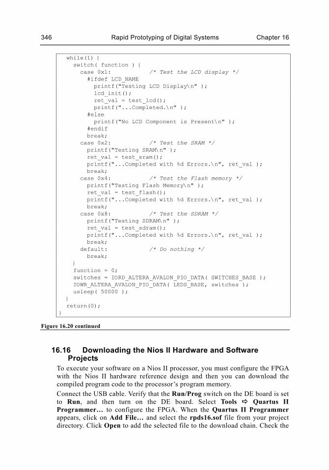
while(1) { switch( function ) { case 0x1: /* Test the LCD display */ #ifdef LCD_NAME printf("Testing LCD Display\n" ); lcd_init(); ret_val = test_lcd(); printf("...Completed.\n" ); #else printf("No LCD Component is Present\n" ); #endif break; case 0x2: /* Test the SRAM */ printf("Testing SRAM\n" ); ret_val = test_sram(); printf("...Completed with %d Errors.\n", ret_val ); break; case 0x4: /* Test the Flash memory */ printf("Testing Flash Memory\n" ); ret_val = test_flash(); printf("...Completed with %d Errors.\n", ret_val ); break; case 0x8: /* Test the SDRAM */ printf("Testing SDRAM\n" ); ret_val = test_sdram(); printf("...Completed with %d Errors.\n", ret_val ); break; default: /* Do nothing */ break; } function = 0; switches = IORD_ALTERA_AVALON_PIO_DATA( SWITCHES_BASE ); IOWR_ALTERA_AVALON_PIO_DATA( LEDS_BASE, switches ); usleep( 50000 ); } return(0); }
Figure 16.20 continued
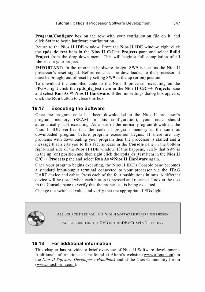
16.16 Downloading the Nios II Hardware and Software Projects
To execute your software on a Nios II processor, you must configure the FPGA with the Nios II hardware reference design and then you can download the compiled program code to the processor’s program memory. Connect the USB cable. Verify that the Run/Prog switch on the DE board is set to Run, and then turn on the DE board. Select Tools Quartus II Programmer… to configure the FPGA. When the Quartus II Programmer appears, click on Add File… and select the rpds16.sof file from your project directory. Click Open to add the selected file to the download chain. Check the
Tutorial III: Nios II Processor Software Development 347
Program/Configure box on the row with your configuration file on it, and click Start to begin hardware configuration. Return to the Nios II IDE window. From the Nios II IDE window, right click the rpds_de_test item in the Nios II C/C++ Projects pane and select Build Project from the drop-down menu. This will begin a full compilation of all libraries in your project. IMPORTANT: In the reference hardware design, SW9 is used as the Nios II processor’s reset signal. Before code can be downloaded to the processor, it must be brought out of reset by setting SW9 in the up (or on) position. To download the compiled code to the Nios II processor executing on the FPGA, right click the rpds_de_test item in the Nios II C/C++ Projects pane and select Run As Nios II Hardware. If the run settings dialog box appears, click the Run button to close this box.
16.17 Executing the Software Once the program code has been downloaded to the Nios II processor’s program memory (SRAM in this configuration), your code should automatically start executing. As a part of the normal program download, the Nios II IDE verifies that the code in program memory is the same as downloaded program before program execution begins. If there are any problems with downloading your program then the processor is stalled and a message that alerts you to this fact appears in the Console pane in the bottom right-hand side of the Nios II IDE window. If this happens, verify that SW9 is in the up (on) position and then right click the rpds_de_test item in the Nios II C/C++ Projects pane and select Run As Nios II Hardware again. Once your program begins executing, the Nios II IDE’s Console pane becomes a standard input/output terminal connected to your processor via the JTAG UART device and cable. Press each of the four pushbuttons in turn. A different device will be tested when each button is pressed and released. Look at the text in the Console pane to verify that the proper test is being executed. Change the switches’ value and verify that the appropriate LEDs light.
ALL SOURCE FILES FOR THIS NIOS II SOFTWARE REFERENCE DESIGN
CAN BE FOUND ON THE DVD IN THE \DEX\CHAP16 DIRECTORY.
16.18 For additional information This chapter has provided a brief overview of Nios II Software development. Additional information can be found at Altera’s website (www.altera.com) in the Nios II Software Developer’s Handbook and at the Nios Community forum (www.niosforum.com).
348 Rapid Prototyping of Digital Systems Chapter 16
16.19 Laboratory Exercises 1. Write a C program to blink the eight green LEDs in a reversing shift pattern on the DE
board. After the last LED in each direction turns on, reverse the direction of the shift. Run and demonstrate the program on the DE board. Recall that C supports shift operations (“<<” and “>>”) and you will need a time delay in your code to see the LEDs blink.
2. Write a C program that displays a count of the seconds that the program has been running in the LCD display on the DE2 board or on the seven-segment displays on the DE1 board. Demonstrate the program on the DE board.
3. Expand the C program in the previous problem to display the elapsed time in hours, minutes, and seconds on the LCD (or seven-segment displays). Have one pushbutton reset the time to zero and another pushbutton start and stop the timer just like a stopwatch.
4. Memory test programs cannot test all possible patterns. Research the various algorithms widely used in more thorough memory test programs and write your own more advanced memory test program for SRAM. Most memory test programs use several algorithms to check for different types of faults. Execute the test code from SDRAM.
5. Write a retro version of the 1970’s classic kill the bit computer game for the DE board. The goal in the kill the bit game is to turn off all of the four LEDs using the four pushbuttons. The game starts with an initial non-zero pattern displayed in the LEDs. The pattern constantly does a circular shift moving through the LEDs in a loop with a time delay to slow down the shifts. If you hit one of the four pushbuttons exactly when the the same number LED is turned on, it will turn off one LED in the pattern. If you hit a pushbutton and it’s LED is off another LED turns on.
Here is how the program works. Each time just before the pattern shifts, the pattern is bit-wise exclusive or’ed with one input sample from the pushbuttons to generate a new pattern. When both the pushbutton is pushed and its corresponding bit in the pattern are High, one less bit will be High in the new pattern after the exclusive or (i.e., 1 xor 1 is 0). After the shift, one less LED will be turned on since there is one less “1” in the new pattern. If your timing is off and the LED is not turned on when you hit the pushbutton, a new high bit will be generated in the pattern (i.e., 1 xor 0 is 1). When this happens, the new “1” bit in the pattern lights another LED. Note that you need a “1” when a pushbutton is pressed and a “1” to turn on an LED for the xor function to work.
Display the elapsed time in the LCD display (or seven-segment displays) and stop the time display when a player wins the game (turns out all LEDs). Adjust the shift time delay for reasonable game play. Blink all of the LEDs when a player wins. If you want a
Tutorial III: Nios II Processor Software Development 349
more challenging game, use a pattern and shift register larger than four bits and just display four bits at a time in the LEDs.
6. Port an interesting C application program to the Nios II processor. Execute the application from SDRAM.