
AN 736: Nios II Processor Booting From Altera …...Nios II Processor Booting From Altera Serial...
17
Nios II Processor Booting From Altera Serial Flash (EPCQ) 2016.05.20 AN-736 Subscribe Send Feedback The Altera ® Nios ® II processor is a soft processor that supports all Altera SoC and FPGA families. This document describes how to boot a Nios II processor from Altera EPCQ flash memory (EPCQx1, EPCQx4) using an Altera serial flash controller. The Altera Serial Flash Controller supports configuring and programming of EPCQx4, EPCQx1 and EPCS flash in FPGA design for Altera Arria ® V, Arria 10, Cyclone V and Stratix ® V devices. Prerequisites You are required to have knowledge in instantiating and developing a system with a Nios II processor. Altera recommends that you go through the online tutorials and training materials provided on Altera's website before using this application note. Related Information • AN 717: Nios II Gen 2 Hardware Development Tutorial Refer to this document for a step-by-step procedure to build a Nios II Gen 2 soft core processor system. • Embedded Peripherals IP User Guide Refer to this document for more information about the Altera serial flash controller. • Quad-Serial Configuration (EPCQ) Devices Datasheet Refer to this document for more information about quad-serial (EPCQ) devices. Definitions The following table defines the acronyms in this application note: Table 1: AN 736 Acronym Definitions Acronym Description ACDS Altera Complete Design Suite API Application Programming Interface CFI Compact Flash Interface EPCQ Altera Quad SPI flash device HAL Hardware Abstraction Layer HEX Hexadecimal file: this is an ASCII text file with the extension of .hex. It stores the initial memory values for a memory block. © 2016 Altera Corporation. All rights reserved. ALTERA, ARRIA, CYCLONE, ENPIRION, MAX, MEGACORE, NIOS, QUARTUS and STRATIX words and logos are trademarks of Altera Corporation and registered in the U.S. Patent and Trademark Office and in other countries. All other words and logos identified as trademarks or service marks are the property of their respective holders as described at www.altera.com/common/legal.html. Altera warrants performance of its semiconductor products to current specifications in accordance with Altera's standard warranty, but reserves the right to make changes to any products and services at any time without notice. Altera assumes no responsibility or liability arising out of the application or use of any information, product, or service described herein except as expressly agreed to in writing by Altera. Altera customers are advised to obtain the latest version of device specifications before relying on any published information and before placing orders for products or services. ISO 9001:2008 Registered www.altera.com 101 Innovation Drive, San Jose, CA 95134
Transcript of AN 736: Nios II Processor Booting From Altera …...Nios II Processor Booting From Altera Serial...
Nios II Processor Booting From Altera Serial Flash(EPCQ)
2016.05.20
AN-736 Subscribe Send Feedback
The Altera® Nios® II processor is a soft processor that supports all Altera SoC and FPGA families. Thisdocument describes how to boot a Nios II processor from Altera EPCQ flash memory (EPCQx1,EPCQx4) using an Altera serial flash controller. The Altera Serial Flash Controller supports configuringand programming of EPCQx4, EPCQx1 and EPCS flash in FPGA design for Altera Arria® V, Arria 10,Cyclone V and Stratix® V devices.
Prerequisites
You are required to have knowledge in instantiating and developing a system with a Nios II processor.Altera recommends that you go through the online tutorials and training materials provided on Altera'swebsite before using this application note.
Related Information
• AN 717: Nios II Gen 2 Hardware Development TutorialRefer to this document for a step-by-step procedure to build a Nios II Gen 2 soft core processorsystem.
• Embedded Peripherals IP User GuideRefer to this document for more information about the Altera serial flash controller.
• Quad-Serial Configuration (EPCQ) Devices DatasheetRefer to this document for more information about quad-serial (EPCQ) devices.
DefinitionsThe following table defines the acronyms in this application note:
Table 1: AN 736 Acronym Definitions
Acronym Description
ACDS Altera Complete Design SuiteAPI Application Programming InterfaceCFI Compact Flash Interface
EPCQ Altera Quad SPI flash deviceHAL Hardware Abstraction LayerHEX Hexadecimal file: this is an ASCII text file with the extension
of .hex. It stores the initial memory values for a memory block.
© 2016 Altera Corporation. All rights reserved. ALTERA, ARRIA, CYCLONE, ENPIRION, MAX, MEGACORE, NIOS, QUARTUS and STRATIX words and logos aretrademarks of Altera Corporation and registered in the U.S. Patent and Trademark Office and in other countries. All other words and logos identified astrademarks or service marks are the property of their respective holders as described at www.altera.com/common/legal.html. Altera warrants performanceof its semiconductor products to current specifications in accordance with Altera's standard warranty, but reserves the right to make changes to anyproducts and services at any time without notice. Altera assumes no responsibility or liability arising out of the application or use of any information,product, or service described herein except as expressly agreed to in writing by Altera. Altera customers are advised to obtain the latest version of devicespecifications before relying on any published information and before placing orders for products or services.
ISO9001:2008Registered
www.altera.com101 Innovation Drive, San Jose, CA 95134

Acronym Description
I/O Input/OutputMemcpy Memory copyOCRAM On-chip RAM
RAM Random Access MemorySBT Software Build ToolsSoC System on a ChipSOF SRAM Object FilesUFM User Flash MemoryXiP Execute in Place
Description of the Altera Serial Flash ControllerThe Altera Serial Flash Controller with Avalon interface allows Nios II processor systems to access AlteraEPCQ flash memory, which supports standard, quad and single- or dual-I/O mode. The Nios II processorSBT supports the Nios II booting from the Altera Serial Flash Controller. In addition, a Nios II hardwareabstraction layer (HAL) driver is available for the Altera Serial Flash Controller that allows an applicationto read, write, or erase flash.
Scenarios for Booting Nios II from EPCQ FlashBooting a Nios II processor from an EPCQ flash has a similar flow to booting a Nios II processor from aCFI flash.
The Nios II processor supports the following two boot options using EPCQ flash:
• The Nios II processor application executes in place from EPCQ flash.• The Nios II processor application is copied from EPCQ flash to RAM using a boot copier.
Table 2: Summary of Nios II Processor Boot Options Using EPCQ Flash
Boot Option Application CodeStored Location
Application Run-timeLocation
Method
Nios II processorapplication executes inplace from EPCQ flash
EPCQ EPCQ (XIP) +OCRAM (for writabledata sections)
Using alt_load() function
Nios II processorapplication is copiedfrom EPCQ flash to
RAM using boot copier
EPCQ OCRAM/ ExternalRAM
Using a memcpy-based bootcopier
Nios II Processor Application Execute-In-Place from EPCQ FlashThe execute-in-place option is suitable for Nios II processor applications which require limited on-chipmemory usage.
2 Description of the Altera Serial Flash ControllerAN-736
2016.05.20
Altera Corporation Nios II Processor Booting From Altera Serial Flash (EPCQ)
Send Feedback
The alt_load() function operates as a mini boot copier which initializes and copies only the writablememory sections to on-chip RAM (OCRAM). The code section (.text), which is a read-only section,remains in the Altera EPCQ flash memory region. Retaining the read-only section in EPCQ helps tominimize RAM use, but may limit the code execution performance. The Nios II processor application isprogrammed into the EPCQ flash.
The Nios II processor reset vector points to the EPCQ flash to allow code execution after the systemresets. If you are debugging the application using the source-level debugger, you must use a hardwarebreakpoint because the EPCQ cannot efficiently support random memory access.
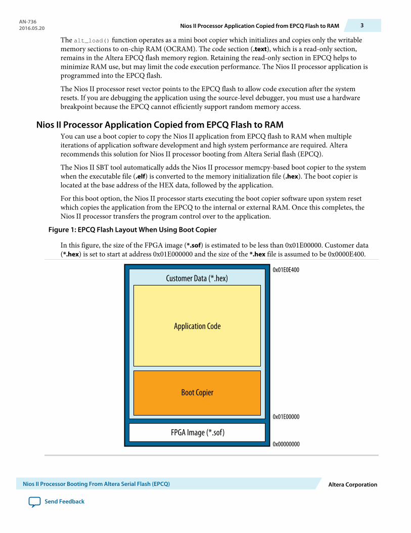
Nios II Processor Application Copied from EPCQ Flash to RAMYou can use a boot copier to copy the Nios II application from EPCQ flash to RAM when multipleiterations of application software development and high system performance are required. Alterarecommends this solution for Nios II processor booting from Altera Serial flash (EPCQ).
The Nios II SBT tool automatically adds the Nios II processor memcpy-based boot copier to the systemwhen the executable file (.elf) is converted to the memory initialization file (.hex). The boot copier islocated at the base address of the HEX data, followed by the application.
For this boot option, the Nios II processor starts executing the boot copier software upon system resetwhich copies the application from the EPCQ to the internal or external RAM. Once this completes, theNios II processor transfers the program control over to the application.
Figure 1: EPCQ Flash Layout When Using Boot Copier
In this figure, the size of the FPGA image (*.sof) is estimated to be less than 0x01E00000. Customer data(*.hex) is set to start at address 0x01E000000 and the size of the *.hex file is assumed to be 0x0000E400.
Customer Data (*.hex)
FPGA Image (*.sof)0x00000000
0x01E00000
Boot Copier
Application Code
0x01E0E400
AN-7362016.05.20 Nios II Processor Application Copied from EPCQ Flash to RAM 3
Nios II Processor Booting From Altera Serial Flash (EPCQ) Altera Corporation
Send Feedback

Nios II Processor Configuration and Boot FlowThis section highlights the design, configuration and BSP settings for the supported boot scenariosmentioned in this document.
Figure 2: Configuration and Booting Flow
DESIGN
• Create your Nios II Processor-based project using Quartus II and Qsys.
• Set the Nios II processor reset and exception vector based on your boot options.• Generate your design in Qsys.• Compile your design in Quartus II.
CONFIGURATION AND COMPILATION
• Create the Nios II processor HAL BSP based on the .sopcinfo file created from Qsys generation.• Edit Nios II processor BSP settings and the Linker Script in the BSP Editor, based on your boot options• Generate BSP
BSP EDITOR SETTINGS
• Develop the Nios II processor application code• Compile the Nios II processor application and generate a HEX file using the mem_init_generate utility
APPLICATION
• Generate a .jic file using the “Convert Programming Files” feature in Quartus II
PROGRAMMING FILES CONVERSION
• Setup the board for Active Serial configuration mode.
CONFIGURATION FOR EPCQ PROGRAMMING
• Using Quartus II programmer, program the .jic file into your device
DOWNLOAD
• Reset your FPGA device using reset button or power cycle your hardware
RESET AND BOOT
4 Nios II Processor Configuration and Boot FlowAN-736
2016.05.20
Altera Corporation Nios II Processor Booting From Altera Serial Flash (EPCQ)
Send Feedback

Steps to Build a Bootable SystemThe following sections describe a step-by-step method for building a bootable system for a:
• Nios II processor application executing in place from EPCQ flash.• Nios II processor application copied from EPCQ flash to RAM using a boot copier.
Design1. Create your Nios II processor project using Quartus II and Qsys.2. Add the Altera Serial Flash Controller IP to your Qsys system. Refer to the diagram below for the IP
connection in Qsys.Figure 3: Altera Serial Flash Controller IP Connections in Qsys
Note: The maximum input clock for Altera Serial Flash Controller IP is 25 MHz. The input clockmust not exceed this maximum value.
Configuration and CompilationTo proceed with configuration and compilation, you must double-click on the Nios II Processor row inthe System Contents window in Qsys to open the Nios II processor Parameters window.
From here, proceed to the "Reset and Vector Settings" section that is applicable to your boot method.
Reset and Exception Vector Settings for Nios II Execute-In-Place Method
1. Under Reset Vector in the Vectors tab, select EPCQ (epcq_controller_0.avl_mem) in the Resetvector memory drop-down menu and type the reset vector offset in the Reset vector offset entry box.The reset vector must be the base address of your application. In this example, it is 0x01E00000.
Note: Your *.sof image size influences your reset vector offset configuration. The reset vector offset isthe start address of the .hex file in EPCQ flash and it must point to a location after the *.sofimage. You can determine the minimum reset vector offset by using the following equation:
minimum reset vector offset= (.sof image start address + .sof image size) in HEX
AN-7362016.05.20 Steps to Build a Bootable System 5
Nios II Processor Booting From Altera Serial Flash (EPCQ) Altera Corporation
Send Feedback

For example, if your *.sof image starts at address 0x0 and is 512 KB in size, then the minimumreset vector offset location you can select is 0x0080000. If the *.sof image space and the resetvector offset location overlap, Quartus® Prime software displays an overlap error.
2. Under Exception Vector, you may select EPCQ (epcq_controller_0.avl_mem) or OCRAM in theException vector memory drop-down menu. In this example, 0x20 is listed for the Exception vectoroffset entry.
Note: When executing-in-place, the Nios II processor boots and runs directly from EPCQ flash,without copying any code at boot time. Because the Nios II begins executing at the reset addressin this case, exception vectors must be located at a nonzero exception vector offset to allow forinstructions between the reset vector and the base of the exception vectors. Thus, you mustinclude an exception vector offset when the reset vector and the exception vector point to thesame memory and no boot copier is present.
Note: Altera recommends setting the exception vector to OCRAM to make the interrupt processingfaster.
Figure 4: Exception Vector Settings in Qsys
3. Click Finish. You will return to the Qsys System Contents tab.4. Double-click on the Altera Serial Flash Controller IP to open the Altera Serial Flash Controller
Parameter editor.5. Select the Configuration device type based on your hardware design and choose the desired I/O
mode.6. Close the Parameter Editor and return to the Qsys System Contents tab.7. Click Generate HDL to generate your Qsys design.8. Compile your design in Quartus Prime software.
Reset and Exception Vector Settings for Nios II Boot Copier Method
1. Under Reset Vector in the Vectors tab, select EPCQ (epcq_controller_0.avl_mem) in the Resetvector memory drop-down menu and type the reset vector offset in the Reset vector offset entry box.The reset vector must be the starting address of your application. In this example, it is 0x01E00000.
6 Reset and Exception Vector Settings for Nios II Boot Copier MethodAN-736
2016.05.20
Altera Corporation Nios II Processor Booting From Altera Serial Flash (EPCQ)
Send Feedback

Note: Your *.sof image size influences your reset vector offset configuration. The reset vector offset isthe start address of the .hex file in EPCQ flash and it must point to a location after the *.sofimage. You can determine the minimum reset vector offset by using the following equation:
minimum reset vector offset= (.sof image start address + .sof image size) in HEX
For example, if your *.sof image starts at address 0x0 and is 512 KB in size, then the minimumreset vector offset location you can select is 0x0080000. If the *.sof image space and the resetvector offset location overlap, Quartus Prime software displays an overlap error.
2. Under Exception Vector, select OCRAM/External RAM in the Exception vector memory drop-down menu. In this example, 0x20 is listed for the Exception vector offset entry.
3. Click Finish. You will return to the Qsys System Contents tab.4. Double-click on the Altera Serial Flash Controller IP to open the Altera Serial Flash Controller
Parameter editor.5. Select the Configuration device type based on your hardware design and choose the desired I/O
mode. Close the Parameter Editor and return to the Qsys System Contents tab.6. Click Generate HDL to generate your Qsys design.7. Compile your design in the Quartus Prime software.
AN-7362016.05.20 Reset and Exception Vector Settings for Nios II Boot Copier Method 7
Nios II Processor Booting From Altera Serial Flash (EPCQ) Altera Corporation
Send Feedback

BSP Editor Settings1. Open the Nios II SBT tool and create the Nios II processor HAL BSP based on the .sopinfo created
from Qsys generation.2. Right-click on the BSP that you have created and select Nios II > BSP Editor.3. Configure the Settings.Advanced.hal.linker and the Linker Section mappings in the BSP Editor
based on your boot options. Refer to the table below.
Table 3: BSP Editor Mappings
Boot Option BSP Editor: Linker Script Settings.Advanced.hal.linker
Nios II processor applica‐tion executes in place fromEPCQ flash
• Set .text Linker Section toEPCQ (epcq_controller_0_avl_mem)
• Set other Linker Sections(.heap, .rwdata, .rodata, .bss, .stack) to OCRAM
If the exception vector is set to OCRAM,enable the following settings inSettings.Advanced.hal.linker:
• allow_code_at_reset• enable_alt_load• enable_alt_load_copy_rodata• enable_alt_load_copy_rwdata• enable_alt_load_copy_exceptions
If the exception vector is set to EPCQ,enable the following settings inSettings.Advanced.hal.linker:
• allow_code_at_reset• enable_alt_load• enable_alt_load_copy_rodata• enable_alt_load_copy_rwdata
Nios II processor applica‐tion is copied from EPCQflash to RAM using bootcopier
Make sure all Linker Sectionsare set to OCRAM/ExternalRAM.
Make sure all settings are left unchecked.
8 BSP Editor SettingsAN-736
2016.05.20
Altera Corporation Nios II Processor Booting From Altera Serial Flash (EPCQ)
Send Feedback
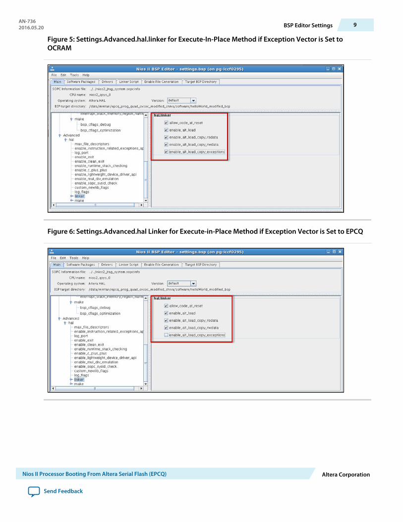
Figure 5: Settings.Advanced.hal.linker for Execute-In-Place Method if Exception Vector is Set toOCRAM
Figure 6: Settings.Advanced.hal Linker for Execute-in-Place Method if Exception Vector is Set to EPCQ
AN-7362016.05.20 BSP Editor Settings 9
Nios II Processor Booting From Altera Serial Flash (EPCQ) Altera Corporation
Send Feedback

Figure 7: Settings.Advanced.hal Linker for Boot Copier Method
Figure 8: Linker Section Mappings for Execute-In-Place Method
10 BSP Editor SettingsAN-736
2016.05.20
Altera Corporation Nios II Processor Booting From Altera Serial Flash (EPCQ)
Send Feedback
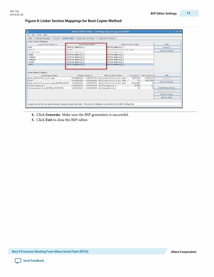
Figure 9: Linker Section Mappings for Boot Copier Method
4. Click Generate. Make sure the BSP generation is successful.5. Click Exit to close the BSP editor.
AN-7362016.05.20 BSP Editor Settings 11
Nios II Processor Booting From Altera Serial Flash (EPCQ) Altera Corporation
Send Feedback

Application1. In the Nios II SBT window, select File > Nios II Application to create a new application. Develop your
Nios II application. Alternatively, you can use a template for the application creation.2. Point your application to the BSP location that you have created in the previous section.3. Once the application development finishes, right-click on the project in Project Explorer and select
Build Project. A *.elf file is create under the project folder.4. Next, generate the HEX file using the mem_init_generate utility. Right-click on the project in Project
Explorer and select Make Targets > Build. The Make Targets window opens as shown below.Figure 10: Make Targets Window
5. Select mem_init_generate and click Build. Make sure epcq_controller_0.hex is created under themem_init folder.
Programming Files Conversion1. In the Quartus Prime software, go to File > Convert Programming Files to open the Convert
Programming File tool.2. Under Output programming file section, set the following items:
12 ApplicationAN-736
2016.05.20
Altera Corporation Nios II Processor Booting From Altera Serial Flash (EPCQ)
Send Feedback
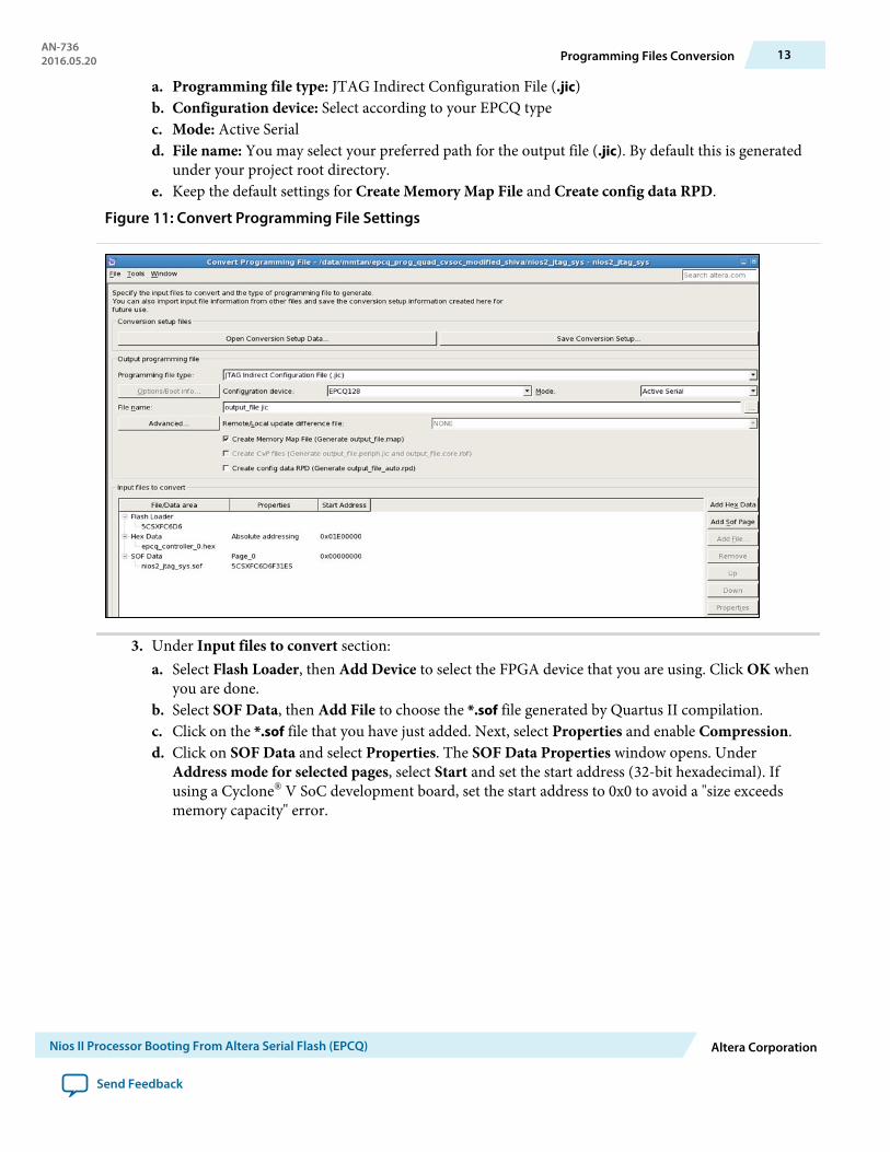
a. Programming file type: JTAG Indirect Configuration File (.jic)b. Configuration device: Select according to your EPCQ typec. Mode: Active Seriald. File name: You may select your preferred path for the output file (.jic). By default this is generated
under your project root directory.e. Keep the default settings for Create Memory Map File and Create config data RPD.
Figure 11: Convert Programming File Settings
3. Under Input files to convert section:a. Select Flash Loader, then Add Device to select the FPGA device that you are using. Click OK when
you are done.b. Select SOF Data, then Add File to choose the *.sof file generated by Quartus II compilation.c. Click on the *.sof file that you have just added. Next, select Properties and enable Compression.d. Click on SOF Data and select Properties. The SOF Data Properties window opens. Under
Address mode for selected pages, select Start and set the start address (32-bit hexadecimal). Ifusing a Cyclone® V SoC development board, set the start address to 0x0 to avoid a "size exceedsmemory capacity" error.
AN-7362016.05.20 Programming Files Conversion 13
Nios II Processor Booting From Altera Serial Flash (EPCQ) Altera Corporation
Send Feedback

Figure 12: SOF Data Properties
e. Click OK to close the window.f. Select Add Hex Data to open the Hex Data Properties window. Select the Absolute addressing
button and browse to the HEX file location. Click OK when you are done.
Note: You may select Relative addressing if you would like to set a relative address to the resetvector offset (0x01E00000) you configured earlier. For example, setting a start address of0x01F00000 for the relative addressing mode changes the start address to 0x3D00000.
14 Programming Files ConversionAN-736
2016.05.20
Altera Corporation Nios II Processor Booting From Altera Serial Flash (EPCQ)
Send Feedback
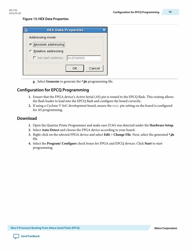
Figure 13: HEX Data Properties
g. Select Generate to generate the *.jic programming file.
Configuration for EPCQ Programming1. Ensure that the FPGA device’s Active Serial (AS) pin is routed to the EPCQ flash. This routing allows
the flash loader to load into the EPCQ flash and configure the board correctly.2. If using a Cyclone V SoC development board, ensure the MSEL pin setting on the board is configured
for AS programming.
Download1. Open the Quartus Prime Programmer and make sure JTAG was detected under the Hardware Setup.2. Select Auto Detect and choose the FPGA device according to your board.3. Right-click on the selected FPGA device and select Edit > Change File. Next, select the generated *.jic
file.4. Select the Program/ Configure check boxes for FPGA and EPCQ devices. Click Start to start
programming.
AN-7362016.05.20 Configuration for EPCQ Programming 15
Nios II Processor Booting From Altera Serial Flash (EPCQ) Altera Corporation
Send Feedback

Figure 14: Quartus II Programmer Window When Programming EPCQ Flash on the Cyclone V SoCDevelopment Board
5. Make sure the download is successful.
Reset and Boot1. Reset your FPGA device using the reset button or power cycle your hardware.
EPCQ HAL DriverThe Nios II hardware abstraction layer (HAL) driver has a generic application programming interface(API) for flash devices.
This API provides you with read and write access to the EPCQ flash through the Altera Serial Flashcontroller for ACDS 15.0 or later. Use driver version 15.0 (or higher) for EPCQ software applicationdevelopment.
Nios II Processor Booting Elements
Memcpy-based Nios II Boot CopierThe Nios II processor memcpy-based boot copier has the following features:
• Supports EPCQ, CFI and Altera on-chip flash (UFM) flash memories• Can locate software application in flash• Unpacks and copies software application image to Random Access Memory (RAM)• Automatically switches to application code in RAM after copy completes
16 Reset and BootAN-736
2016.05.20
Altera Corporation Nios II Processor Booting From Altera Serial Flash (EPCQ)
Send Feedback

The Nios II processor boot copier is used when the Nios II soft processor application is copied fromEPCQ flash to RAM. The memcpy-based boot copier is automatically appended to the .hex file by theNios II SBT tool when the executable file (.elf) is converted to a memory initialization file (.hex) using themake mem_init_generate target. This operation takes place whenever the .text linker section is locatedin a different memory than where the reset vector points, which indicates a code copy is required. Thefunction of the boot copier is to copy the software application to your desired location such as RAM.Once the copy is complete, the boot copier passes the system control to the application.
Related InformationAN 730: Nios II Processor Booting Methods in MAX 10 DevicesRefer to this information for more information about Nios II processor booting elements.
Revision History for Nios II Booting From Altera Serial Flash (EPCQ)Date Version Changes
May 2016 2016.05.20 Clarified notes for reset exception vector offset in the Configuration andCompilation section.
January 2016 2016.01.19 Clarified notes for *.sof image and exception vector found in theConfiguration and Compilation section.
May 2015 2015.05.26 Changed .hex file size in "Nios II Processor Application Copied fromEPCQ Flash to RAM" section.
May 2015 2015.05.04 Initial Release
AN-7362016.05.20 Revision History for Nios II Booting From Altera Serial Flash (EPCQ) 17
Nios II Processor Booting From Altera Serial Flash (EPCQ) Altera Corporation
Send Feedback