Nios Development Board Reference Manual, Stratix - Altera
50
Reference Manual, Stratix Professional Edition Nios Development Board 101 Innovation Drive San Jose, CA 95134 (408) 544-7000 www.altera.com Document Version: 1.1 Document Date: July 2003
Transcript of Nios Development Board Reference Manual, Stratix - Altera

Reference Manual, Stratix Professional Edition
Nios Development Board
101 Innovation DriveSan Jose, CA 95134(408) 544-7000www.altera.com
Document Version: 1.1Document Date: July 2003

ii Altera CorporationMNL-NIOSSTXPRO-1.1
Copyright Nios Development Board Reference Manual, Stratix Professional Edition
Copyright © 2003 Altera Corporation. All rights reserved. Altera, The Programmable Solutions Company, the stylized Altera logo, specific device designations, and all other words and logos that are identified as trademarks and/or service marks are, unless noted otherwise, the trademarks and service marks of Altera Corporation in the U.S. and other countries. All other product or service names are the property of their respective holders. Altera products are protected under numerous U.S. and foreign patents and pending applications, mask work rights, and copyrights. Altera warrants performance of its semiconductor products to current specifications in accordance with Altera’s standard warranty, but reserves the right to make changes to any products and services at any time without notice. Altera assumes no responsibility or liability arising out of the application or use of any information, product, or service described herein except as expressly agreed to in writing by Altera Corporation. Altera customers are advised to obtain the latest version of device specifications before relying on any published information and before placing orders for products or services.

Altera Corporation
About this Manual
This manual provides component details about the Nios development board, Stratix Professional edition.
Table 1 shows the reference manual revision history.
How to Find Information
■ The Adobe Acrobat Find feature allows you to search the contents of a PDF file. Click the binoculars toolbar icon to open the Find dialog box.
■ Bookmarks serve as an additional table of contents.■ Thumbnail icons, which provide miniature previews of each page,
provide a link to the pages.■ Numerous links, shown in green text, allow you to jump to related
information.
Table 1. Reference Manual Revision History
Date Description
July 2003 Reflects new directory structure for SOPC Builder 3.0 and Nios Development Kit version 3.1.
May 2003 First publication for the Nios Development Kit, Stratix Professional Edition development board.
iii

About this Manual Nios Development Board Reference Manual, Stratix Professional Edition
How to Contact Altera
For the most up-to-date information about Altera products, go to the Altera world-wide web site at http://www.altera.com.
For technical support on this product, go to http://www.altera.com/mysupport. For additional information about Altera products, consult the sources shown in Table 2.
Note:(1) You can also contact your local Altera sales office or sales representative.
Table 2. How to Contact Altera
Information Type USA & Canada All Other Locations
Product literature http://www.altera.com http://www.altera.com
Altera literature services [email protected] (1) [email protected] (1)
Non-technical customer service
(800) 767-3753 (408) 544-7000 (7:30 a.m. to 5:30 p.m. Pacific Time)
Technical support (800) 800-EPLD (3753)(7:30 a.m. to 5:30 p.m. Pacific Time)
(408) 544-7000 (1)(7:30 a.m. to 5:30 p.m. Pacific Time)
http://www.altera.com/mysupport/ http://www.altera.com/mysupport/
FTP site ftp.altera.com ftp.altera.com
iv Altera Corporation

Nios Development Board Reference Manual, Stratix Professional Edition About this Manual
Typographic Conventions
This document uses the typographic conventions shown in Table 3.
Table 3. Conventions
Visual Cue Meaning
Bold Type with Initial Capital Letters
Command names, dialog box titles, checkbox options, and dialog box options are shown in bold, initial capital letters. Example: Save As dialog box.
bold type External timing parameters, directory names, project names, disk drive names, filenames, filename extensions, and software utility names are shown in bold type. Examples: fMAX, \QuartusII directory, d: drive, chiptrip.gdf file.
Bold italic type Book titles are shown in bold italic type with initial capital letters. Example: 1999 Device Data Book.
Italic Type with Initial Capital Letters
Document titles are shown in italic type with initial capital letters. Example: AN 75 (High-Speed Board Design).
Italic type Internal timing parameters and variables are shown in italic type. Examples: tPIA, n + 1.Variable names are enclosed in angle brackets (< >) and shown in italic type. Example: <file name>, <project name>.pof file.
Initial Capital Letters Keyboard keys and menu names are shown with initial capital letters. Examples: Delete key, the Options menu.
“Subheading Title” References to sections within a document and titles of Quartus II Help topics are shown in quotation marks. Example: “Configuring a FLEX 10K or FLEX 8000 Device with the BitBlaster™ Download Cable.”
Courier type Signal and port names are shown in lowercase Courier type. Examples: data1, tdi, input. Active-low signals are denoted by suffix n, e.g., resetn.
Anything that must be typed exactly as it appears is shown in Courier type. For example: c:\quartusII\qdesigns\tutorial\chiptrip.gdf. Also, sections of an actual file, such as a Report File, references to parts of files (e.g., the AHDL keyword SUBDESIGN), as well as logic function names (e.g., TRI) are shown in Courier.
1., 2., 3., and a., b., c.,... Numbered steps are used in a list of items when the sequence of the items is important, such as the steps listed in a procedure.
■ Bullets are used in a list of items when the sequence of the items is not important.
v The checkmark indicates a procedure that consists of one step only.
1 The hand points to information that requires special attention.
r The angled arrow indicates you should press the Enter key.
f The feet direct you to more information on a particular topic.
Altera Corporation v


Table of Contents
About this Manual ...................................................................................................................................... iiiHow to Find Information.............................................................................................................. iiiHow to Contact Altera .................................................................................................................. ivTypographic Conventions .............................................................................................................. vFeatures ............................................................................................................................................. 9General Description......................................................................................................................... 9
Default Reference Design ....................................................................................................... 9
Board Components ......................................................................................................................................9Restoring the Default Reference Design to the Board ...................................................... 10Block Diagram ........................................................................................................................ 11
Nios Development Board Components...................................................................................... 12The Stratix EP1S40 Device ............................................................................................................ 13Flash Memory Device.................................................................................................................... 13Compact Flash Connector............................................................................................................. 14SDRAM Device............................................................................................................................... 16Dual SRAM Devices ...................................................................................................................... 18Ethernet MAC/PHY...................................................................................................................... 19Expansion Prototype Connector (PROTO1) .............................................................................. 19Expansion Prototype Connector (PROTO2) .............................................................................. 21Mictor Connector ........................................................................................................................... 23Serial Port Connectors ................................................................................................................... 25Dual Seven-Segment Display....................................................................................................... 26Push-Button Switches.................................................................................................................... 27Individual LEDs ............................................................................................................................. 27Configuration Controller Device (EPM7128AE) ....................................................................... 27
Reset Distribution .................................................................................................................. 27Starting Configuration .......................................................................................................... 28Stratix Configuration............................................................................................................. 28Configuration Data ................................................................................................................ 28Safe and User Configurations .............................................................................................. 29
Using Conventional Flash Memory ............................................................................ 29The Configuration-Status LEDs........................................................................................... 33Configuration and Reset Buttons ........................................................................................ 34
SW8 – CPU Reset ........................................................................................................... 34SW9 – Safe Config.......................................................................................................... 34SW10 – Reset, Config..................................................................................................... 34
Power-Supply Circuitry................................................................................................................ 35Clock Circuitry ............................................................................................................................... 35
Altera Corporation vii

Table of Contents Nios Development Board Reference Manual, Stratix Professional Edition
JTAG Connections ......................................................................................................................... 36JTAG to Stratix Device (J24) ................................................................................................. 36JTAG to MAX Device (J5) ..................................................................................................... 38
Appendix A: Shared Bus Table .............................................................................................................39
Appendix B: Restore the Factory Configuration ...............................................................................43Configuring the Stratix Device .................................................................................................... 43Reprogramming the Flash Memory............................................................................................ 44
Appendix C: Board Ethernet Connection ............................................................................................45Connecting the Ethernet Cable ............................................................................................ 45Connecting the LCD Display ............................................................................................... 46Obtaining an IP address: DHCP .......................................................................................... 46
IP Addresses for Point–to–Point Connections........................................................... 47IP Addresses for LAN Connections ............................................................................ 48
Browsing your Board ............................................................................................................ 48
Index ................................................................................................................................................................49
viii Altera Corporation

Board Components
Features ■ A StratixTM EP1S40F780C5 device■ 8 Mbytes of flash memory■ 1 Mbyte of static RAM ■ 16 Mbytes of SDRAM ■ On board logic for configuring the Stratix Professional device from
flash memory■ On-board Ethernet MAC/PHY device■ Two 5-V-tolerant expansion/prototype headers each with access to
41 Stratix Professional user I/O pins■ CompactFlashTM connector header for Type I Compact Flash (CF)
cards ■ Mictor connector for hardware and software debug■ Two RS-232 DB9 serial ports■ Four push-button switches connected to Stratix Professional user I/O
pins■ Eight LEDs connected to Stratix Professional user I/O pins■ Dual 7-segment LED display■ JTAG connectors to Altera® devices via Altera download cables■ 50 MHz Oscillator and zero-skew clock distribution circuitry■ Power-on reset circuitry
General Description
The Nios development board, Stratix professional edition, provides a hardware platform for developing embedded systems based on Altera Stratix devices. The Nios development board features a Stratix EP1S40F780C5 device with 41,250 logic elements (LEs) and 3,423,744 Kbits of on-chip memory.
The Nios development board comes pre-programmed with a 32-bit Nios processor reference design. Hardware designers can use the reference design as an example of how to use the features of the Nios development board. Software designers can use the pre-programmed Nios processor design on the board to begin prototyping software immediately.
Default Reference Design
When power is applied to the board, the on-board configuration logic configures the Stratix FPGA using hardware configuration data stored in flash. When the device is configured, the Nios processor design in the FPGA wakes up and begins executing boot code from flash memory.
Altera Corporation 9

Board Components Nios Development Board Reference Manual, Stratix Professional Edition
The default reference design provides facilities to download new, user-defined software and hardware configuration data to the board from a host computer. Download methods include a serial cable, a JTAG download cable, or an Ethernet cable. The GERMS monitor, an Altera-provided monitor program for the Nios processor, is running on the Console RS-232 serial port (J19). Simultaneously, a web server program is running via the ethernet connection.
1 The Ethernet port provides a very fast and easy method to download hardware and software images to the board via a web browser on your host computer. For instructions on communicating with your Nios development board via Ethernet, see “Appendix C: Board Ethernet Connection” on page 45.
f See the Nios Development Kit, Stratix Professional Edition Getting Started User Guide for instructions on setting up the Nios development board. See the Nios Hardware Development Tutorial for instructions on using this pre-loaded reference design.
Restoring the Default Reference Design to the Board
In the course of development, you may overwrite or erase the flash memory space containing the default reference design. Altera provides the flash image for the default reference design, so that you can always return the board to its default state. These default reference files are located in the Nios development kit examples directory.
See “Appendix B: Restore the Factory Configuration” on page 43 for more information.
10 Altera Corporation

Nios Development Board Reference Manual, Stratix Professional Edition Board Components
Block Diagram
Figure 1 shows a block diagram of the board.
Figure 1. Nios Development Board, Stratix Professional Edition Block Diagram
Altera Corporation 11

Board Components Nios Development Board Reference Manual, Stratix Professional Edition
Nios Development Board Components
This section contains a brief overview of important components on the Nios development board (see Figure 2). Links to the component manufacturers are included when available.
A complete set of schematics, a physical layout database, and GERBER files for the Nios development board are installed in the documents directory for the Nios development kit.
Figure 2. Nios Development Board Components
12 Altera Corporation

Nios Development Board Reference Manual, Stratix Professional Edition Board Components
The Stratix EP1S40 Device
U53 is a Stratix EP1S40F780C5 device in a 780-pin FineLine BGA® package. Table 1 lists the Stratix device features.
The development board provides two separate methods for configuring the Stratix device:
1. Using the Quartus II software running on a host computer, a designer configures the device directly via an Altera download cable connected to the Stratix JTAG header (J24).
2. When power is applied to the board, a configuration controller device (U3) attempts to configure the Stratix device with hardware configuration data stored in flash memory. For more information on the configuration controller, see “Configuration Controller Device (EPM7128AE)” on page 27.
f See the Altera Stratix literature page for Stratix-related documentation at www.altera.com/literature/lit-stx.html including a Stratix EP1S40 pinout document.
Flash Memory Device
U5 is an 8 Mbyte AMD AM29LV065D flash memory device connected to the Stratix device and can be used for two purposes:
1. A Nios embedded processor implemented on the Stratix device can use the flash memory as general-purpose readable memory and non-volatile storage.
2. The flash memory can hold Stratix configuration data that is used by the configuration controller to load the Stratix device at power-up. See “Configuration Controller Device (EPM7128AE)” on page 27. for related information.
Table 1. Stratix 1S40 Device Features
Logic Elements 41,250
M512 RAM blocks (32 x 18 bits) 384
M4K RAM blocks (128 x 36 bits) 183
M-RAM blocks (4K x 144 bits) 4
Total RAM bits 3,423,744
DSP blocks 6
Embedded multipliers 48
PLLs 12
Maximum user I/O pins 822
Altera Corporation 13

Board Components Nios Development Board Reference Manual, Stratix Professional Edition
Hardware configuration data that implements the Nios reference design is pre-stored in this flash memory. The pre-loaded Nios reference design, once loaded, can identify the 8 Mbyte flash memory in its address space and includes monitor software that can download files (either new Stratix configuration data, Nios embedded processor software, or both) into flash memory. The Nios embedded processor software includes subroutines for writing and erasing this specific type of AMD flash memory.
The flash memory device shares address and data connections with the SRAM chips and the Ethernet MAC/PHY chip. For shared bus information, see“Appendix A: Shared Bus Table” on page 39.
f See www.amd.com for detailed information about the flash memory device.
Compact Flash Connector
The compact flash connector (CON3) enables hardware designs to access a compact flash card (see Figure 3). The following two access modes are supported:
■ ATA (hot swappable mode)■ IDE (IDE hard disk mode)
Figure 3. Compact Flash Connector
The IDE connection mode includes a power MOSFET which controls power to the compact flash card. This MOSFET is controllable through an IO pin on the Stratix device.
1 The compact flash connector shares several Stratix I/O pins with expansion prototype connector header (PROTO1), see “Expansion Prototype Connector (PROTO1)” on page 19 for PROTO1 details.
14 Altera Corporation

Nios Development Board Reference Manual, Stratix Professional Edition Board Components
Table 2 below provides compact flash pin out details
Table 2. Compact Flash (CON3) Pin Table (Part 1 of 2)
Stratix Device Pin (U53)
Compact Flash Pin (CON3)
Compact Flash Function
GND 1 GND
M4 2 D03
N6 3 D04
N1 4 D05
N9 5 D06
P3 6 D07
J2 7 -CE
M7 8 A10
K7 9 -OE
K3 10 A09
H3 11 A08
L7 12 A07
VCC 13 VCC
L8 14 A06
H2 15 A05
H1 16 A04
L6 17 A03
L10 18 A02
J3 19 A01
L9 20 A00
N3 21 D00
L2 22 D01
N8 23 D02
K4 24 WP
GND 25 -CD2
R3 26 -CD1
M3 27 D11
N7 28 D12
L1 29 D13
N4 30 D14
L3 31 D15
K8 32 -CE2
GND 33 -VS1
M9 34 -OIORD
Altera Corporation 15

Board Components Nios Development Board Reference Manual, Stratix Professional Edition
f See www.molex.com for more compact flash connector (CON3) information. See www.compactflash.org for more information on the compact flash connector.
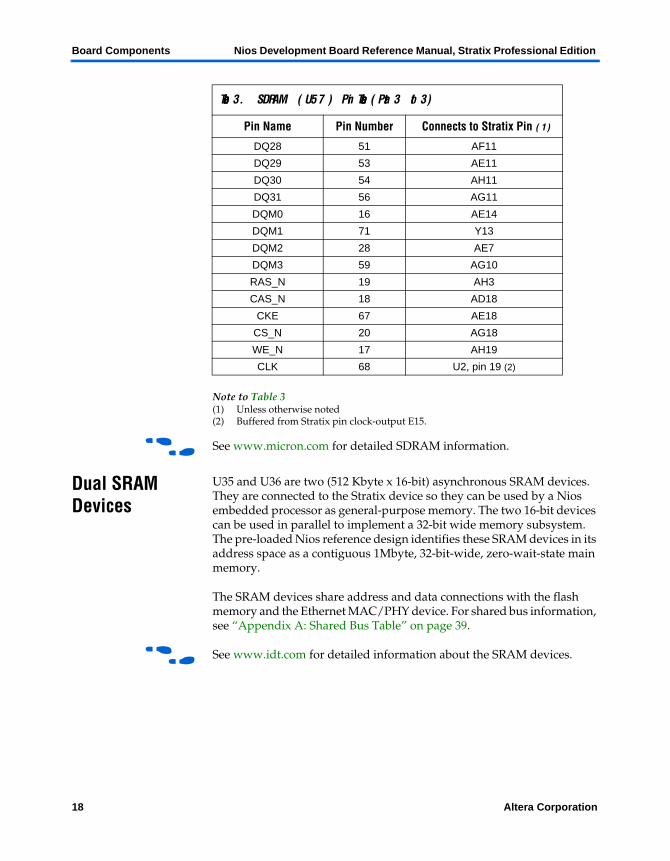
SDRAM Device The SDRAM device (U57) is a Micron MT48LC4M32B2 chip with PC100 functionality and self refresh mode. The SDRAM is fully synchronous with all signals registered on the positive edge of the system clock (clk).
The SDRAM device pins are connected to the Stratix device (see Table 3). An SDRAM controller peripheral is included with the Nios development kit, allowing a Nios processor to view the SDRAM device as a large, linearly addressable memory.
M10 35 -IOWR
L5 36 -WE
M5 37 RDY/BSY
VCC 38 VCC
GND 39 -CSEL
NC 40 -VS2
RESET_n 41 RESET
K1 42 -WAIT
J4 43 -INPACK
G2 44 -REG
J1 45 BVD2
M8 46 BVD1
N10 47 D081
M2 48 D091
N5 49 D101
GND 50 GND
Table 2. Compact Flash (CON3) Pin Table (Part 2 of 2)
Stratix Device Pin (U53)
Compact Flash Pin (CON3)
Compact Flash Function
Table 3. SDRAM (U57) Pin Table (Part 1 of 3)
Pin Name Pin Number Connects to Stratix Pin (1)
A0 25 AE4
A1 26 W12
A2 27 AC11
A3 60 W10
16 Altera Corporation

Nios Development Board Reference Manual, Stratix Professional Edition Board Components
A4 61 AA11
A5 62 AC10
A6 63 AB11
A7 64 AC8
A8 65 AB10
A9 66 V11
A10 24 Y11
A11 21 AB7
BA0 22 AG19
BA1 23 AF19
DQ0 2 AH4
DQ1 4 AE5
DQ2 5 AG3
DQ3 7 AG5
DQ4 8 AG4
DQ5 10 AF4
DQ6 11 AH5
DQ7 13 AF5
DQ8 74 AE6
DQ9 76 AG6
DQ10 77 AH6
DQ11 79 AD6
DQ12 80 AF7
DQ13 82 AH7
DQ14 83 AG7
DQ15 85 AF6
DQ16 31 AG8
DQ17 33 AF8
DQ18 34 AD8
DQ19 36 AH9
DQ20 37 AH8
DQ21 39 AE9
DQ23 42 AG9
DQ24 45 AD10
DQ25 47 AF10
DQ26 48 AH10
DQ27 50 AE10
Table 3. SDRAM (U57) Pin Table (Part 2 of 3)
Pin Name Pin Number Connects to Stratix Pin (1)
Altera Corporation 17
Board Components Nios Development Board Reference Manual, Stratix Professional Edition
Note to Table 3(1) Unless otherwise noted(2) Buffered from Stratix pin clock-output E15.
f See www.micron.com for detailed SDRAM information.
Dual SRAM Devices
U35 and U36 are two (512 Kbyte x 16-bit) asynchronous SRAM devices. They are connected to the Stratix device so they can be used by a Nios embedded processor as general-purpose memory. The two 16-bit devices can be used in parallel to implement a 32-bit wide memory subsystem. The pre-loaded Nios reference design identifies these SRAM devices in its address space as a contiguous 1Mbyte, 32-bit-wide, zero-wait-state main memory.
The SRAM devices share address and data connections with the flash memory and the Ethernet MAC/PHY device. For shared bus information, see “Appendix A: Shared Bus Table” on page 39.
f See www.idt.com for detailed information about the SRAM devices.
DQ28 51 AF11
DQ29 53 AE11
DQ30 54 AH11
DQ31 56 AG11
DQM0 16 AE14
DQM1 71 Y13
DQM2 28 AE7
DQM3 59 AG10
RAS_N 19 AH3
CAS_N 18 AD18
CKE 67 AE18
CS_N 20 AG18
WE_N 17 AH19
CLK 68 U2, pin 19 (2)
Table 3. SDRAM (U57) Pin Table (Part 3 of 3)
Pin Name Pin Number Connects to Stratix Pin (1)
18 Altera Corporation

Nios Development Board Reference Manual, Stratix Professional Edition Board Components
Ethernet MAC/PHY
The LAN91C111 (U4) is a mixed signal analog/digital device that implements protocols at 10Mbps and 100 Mbps. The control pins of U4 are connected to the Stratix device so that Nios systems can access Ethernet via the RJ-45 connector (RJ1). See Figure 4. The Nios development kit includes hardware and software components that allow Nios processor systems to communicate with the LAN91C111 Ethernet device.
Figure 4. Ethernet MAC/PHY Device
The Ethernet MAC/PHY device share address and data connections with the flash memory and the SRAM chips. For shared bus information, see “Appendix A: Shared Bus Table” on page 39.
f See www.smsc.com for detailed information about the LAN91C111 device. See the Plugs Ethernet Library Reference Manual for details on accessing the MAC/PHY device in Nios software.
Expansion Prototype Connector (PROTO1)
The PROTO1 expansion prototype connectors share Stratix IO pins with the compact flash connector. Designs may use either the PROTO1 connectors or the compact flash.
Headers J11, J12, and J13 collectively form the standard-footprint, mechanically-stable connection that can be used (for example) as an interface to a special-function daughter card.
1 See the Altera web site for a list of available expansion daughter cards that can be used with the Nios development board at www.altera.com/devkits.
The expansion prototype connector interface includes:
■ 41 I/O pins for prototyping. All 41 I/O pins connect to user I/O pins on the Stratix device. Each signal passes through analog switches (U19, U20, U21, U22 and U25) to protect the Stratix device from 5-V logic levels. These analog switches are permanently enabled.
■ A buffered, zero-skew copy of the on-board OSC output (from U2).■ A buffered, zero-skew copy of the Cyclone's phase-locked loop
(PLL)-output (from U53)■ A logic-negative power-on-reset signal■ Five regulated 3.3-V power-supply pins (2A total max load for both
PROTO1 & PROTO2)
Altera Corporation 19

Board Components Nios Development Board Reference Manual, Stratix Professional Edition
■ One regulated 5-V power-supply pin (1A total max load for both PROTO1 &PROTO2)
■ Numerous ground connections
The output logic level on the expansion prototype connector pins is 3.3V. The power supply included with the Nios development kit cannot supply the maximum load current specified above.
Figure 5, Figure 6 and Figure 7 on page 21 show connections from the PROTO1 expansion headers to the Stratix device. Unless otherwise noted, labels indicate Stratix device pin numbers.
Figure 5. Expansion Prototype Connector - J11
20 Altera Corporation

Nios Development Board Reference Manual, Stratix Professional Edition Board Components
Figure 6. Expansion Prototype Connector - J12
Figure 7. Expansion Prototype Connector - J13
Note to Figure 7(1) Unregulated voltage from AC to DC power transformer.(2) Clk from board oscillator.(3) Clk from PLD via buffer.(4) Clk output from protocard to PLD.
Expansion Prototype Connector (PROTO2)
Headers J15, J16, and J17 collectively form the standard-footprint, mechanically-stable connection that can be used (for example) as an interface to a special-function daughter card.
The expansion prototype connector interface includes:
■ 41 I/O pins for prototyping. All 41 I/O pins connect to user I/O pins on the Stratix device. Each signal passes through analog switches (U27, U28, U29, U30 and U31) to protect the Stratix device from 5-V logic levels. These analog switches are permanently enabled.
■ A buffered, zero-skew copy of the on-board OSC output (from U2).■ A buffered, zero-skew copy of the Cyclone's phase-locked loop
(PLL)-output (from U53)■ A logic-negative power-on-reset signal
Altera Corporation 21

Board Components Nios Development Board Reference Manual, Stratix Professional Edition
■ Five regulated 3.3-V power-supply pins (2A total max load for both PROTO1 &PROTO2)
■ One regulated 5-V power-supply pin (1A total max load for both PROTO1 &PROTO2)
■ Numerous ground connections
The output logic level on the expansion prototype connector pins is 3.3V. The power supply included with the Nios development kit cannot supply the maximum load current specified above.
Figure 8, Figure 9 on page 23 and Figure 10 on page 23 show connections from the PROTO2 expansion headers to the Stratix device. Unless otherwise noted, labels indicate Stratix device pin numbers.
Figure 8. Expansion Prototype Connector - J16
22 Altera Corporation

Nios Development Board Reference Manual, Stratix Professional Edition Board Components
Figure 9. Expansion Prototype Connector - J15
Figure 10. Expansion Prototype Connector - J17
Note to Figure 10(1) Unregulated voltage from AC to DC power transformer.(2) Clk from board oscillator.(3) Clk from PLD via buffer.(4) Clk output from protocard to PLD.
Mictor Connector
The Mictor connector (J25) can be used to transmit up to 27 high-speed I/O signals with very low noise via a shielded Mictor cable. J25 is used as a debug port. Twenty five of the Mictor connector signals are used as data, and two signals are used as clock input and clock output.
Most pins on J25 connect to I/O pins on the Stratix device (U53). For systems that do not use the Mictor connector for the Nios on-chip instrumentation (OCI)™ debug module, any on-chip signals can be routed to I/O pins and probed at J25 via a Mictor cable. External scopes and logic analyzers can connect to J25 and analyze a large number of signals simultaneously.
Altera Corporation 23

Board Components Nios Development Board Reference Manual, Stratix Professional Edition
1 The Nios OCI debug module is the First Silicon Solutions Inc. (FS2) OCI core.
f See the Nios Development Software Tutorial for the more information about the OCI debug module.
Figure 11 shows an example of an in-target system analyzer ISA-NIOS/T (sold separately) by First Silicon Solutions (FS2) Inc. For details see www.fs2.com.
Figure 11. Mictor Debug Port to OCI Debug Module
Five of the signals connect directly to the JTAG pins on the Stratix device (U53), and also connect directly to the Stratix device’s JTAG connector (J24). The JTAG signals have special usage requirements. You cannot use J24 and J25 at the same time.
Figure 12 below shows connections from the Mictor connector to the Stratix device. Figure 13 shows the pin out for J25. Unless otherwise noted, labels indicate Stratix device pin numbers.
Figure 12. Mictor Connector Signaling
24 Altera Corporation

Nios Development Board Reference Manual, Stratix Professional Edition Board Components
Figure 13. Debug Mictor Connector - J25
Serial Port Connectors
J19 & J27 are standard DB-9 serial connectors. These connectors are typically used for communication with a host computer using a standard, 9-pin serial cable connected to (for example) a COM port. Level-shifting buffers (U52 and U58) are used between J19 & J27 and the Stratix device, because the Stratix device cannot interface to RS-232 voltage levels directly.
The Nios development board provides two serial connectors, one labeled Console and the other labeled Debug. Many processor systems make use of multiple UART communication channels during prototype and debug stages.
The console serial port is able to transmit all RS-232 signals. Alternately, the Stratix design may use only the signals it needs, such as RXD and TXD. LEDs are connected to the RXD and TXD signals, giving a visual indication when data is being transmitted or received. Figure 14 and Figure 15 show the pin connections between the Console and Debug serial connectors and the Stratix device.
Altera Corporation 25

Board Components Nios Development Board Reference Manual, Stratix Professional Edition
Figure 14. Console Serial Port Connector - J19
Figure 15. Debug Serial Port Connector – J27
Dual Seven-Segment Display
U8 and U9 are connected to the Stratix device so that each segment is individually controlled by a general-purpose I/O pin. When the Stratix pin drives logic 0, the corresponding LED turns on. See Figure 16 for Stratix device pin out details.
Figure 16. Dual-7-Segment Display
The pre-loaded Nios reference design includes parallel input/output (PIO) registers and logic for driving this display.
26 Altera Corporation

Nios Development Board Reference Manual, Stratix Professional Edition Board Components
Push-Button Switches
SW0 – SW3 are momentary-contact push-button switches and are used to provide stimulus to designs in the Stratix device. See Figure 17 on page 27. Each switch is connected to an Stratix general-purpose I/O pin with a pull-up resistor as shown in Table 4. The Stratix device pin will see a logic 0 when each switch is pressed.
Individual LEDs This Nios development board provides eight individual LEDs connected to the Stratix device. See Figure 17 on page 27. D0 – D7 are connected to general purpose I/O pins on the Stratix device as shown in Table 5. When the Stratix pin drives logic 1, the corresponding LED turns on.
Figure 17. SW0 – SW3 Push Button Switches and Individual LEDs
Configuration Controller Device (EPM7128AE)
The configuration controller (U3), is an Altera EPM7128AE device. It comes pre-programmed with logic for managing board reset conditions and configuring the Stratix device from data stored in flash memory.
Reset Distribution
The EPM7128AE takes a power-on reset pulse from the Linear Technologies 1326 power-sense/reset-generator chip and distributes it (through internal logic) to other reset-pins on the board, including the:
■ LAN91C111 (Ethernet MAC/PHY) reset■ Flash memory reset
Table 4. Push Button Switches Pin Out Table
Button SW0 SW1 SW2 SW3
Stratix Pin W5 W6 AB2 AB1
Table 5. LED Pin Out Table
LED D0 D1 D2 D3 D4 D5 D6 D7
Stratix Pin H27 H28 L23 L24 J25 J26 L20 L19
Altera Corporation 27

Board Components Nios Development Board Reference Manual, Stratix Professional Edition
■ Reset signals delivered to the expansion prototype connector headers (PROTO1 & PROTO2)
Starting Configuration
There are four methods to start a configuration sequence. The four methods are the following:
1. Board power-on.
2. Pressing the Reset, Config button (SW10).
3. Asserting (driving 0 volts on) the MAX's reconfigreq_n input pin (from a Stratix design).
4. Pressing the Safe Config button (SW9).
Stratix Configuration
At power-up or reset, the configuration controller reads data out of the flash memory, and presents the necessary control signals to configure the Stratix device. The Stratix device is configured using fast passive parallel mode.
Most users will never need to re-program the configuration controller. Reprogramming the configuration controller may result in an inoperable development board. A programming file (config_controller.pof) with the original configuration controller logic is included with the Nios development kit. If you have changed the MAX device logic, you can restore the factory configuration using this programming file located in the EPM7128_flash_config_ controller folder of the examples directory for this board.
See the MAX7000 device literature at www.altera.com/literature/lit-m7k.html for detailed information about the Altera EPM7128AE device (Altera MAX® 7000 family).
Configuration Data
The Quartus II software can (optionally) produce hexout configuration files that are directly suitable for download and storage in the flash memory as configuration data. A hexout configuration file for the Stratix EP1S40 device (U53) is about 1.5 Mbyte, and stored in the flash memory.
28 Altera Corporation

Nios Development Board Reference Manual, Stratix Professional Edition Board Components
New hexout files can be stored in the flash memory (U5) by software running on a Nios embedded processor. The Nios pre-loaded reference design includes facilities for downloading hexout files from a host (such as desktop workstation) into flash memory.
f See the Nios Embedded Processor Software Development Reference Manual for detailed information.
Safe and User Configurations
The configuration controller can manage two separate Stratix device configurations stored in flash memory. These two configurations stored in flash memory are conventionally referred to as the safe configuration and the user configuration. Upon reset or when the Reset, Config button (SW10) is pressed, the configuration controller will attempt to load the Stratix device with user configuration data. If this process fails (either because the user-configuration is invalid or not present), the configuration controller will then load the Stratix device with safe configuration data.
The configuration controller expects user configuration and safe configuration files to be stored at fixed locations (offsets) in flash memory. Table 7 on page 32 shows how the configuration controller expects flash memory contents to be arranged.
1 A Nios reference design is pre-loaded into the safe-configuration region of the flash memory. Altera recommends that users avoid overwriting the safe configuration data.
When SW9 (Safe Config) is pressed, the configuration controller will ignore the user-configuration and always configure the Stratix device from the safe configuration.This switch allows you to “escape” from the situation where a valid-but-nonfunctional user configuration is present in flash memory.
f See the Nios Embedded Processor Software Development Reference Manual for detailed information about downloading and relocating files using the GERMS monitor.
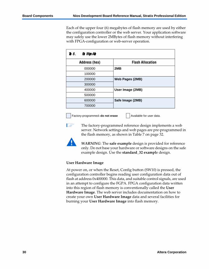
Using Conventional Flash Memory
The Nios Development Board includes an 8 MByte flash memory chip (U5) as shown in Table 6. It is divided into 128 individually-erasable 64K sectors. This web-server design, and (more importantly) the on-board configuration controller, makes certain assumptions about what–resides–where in flash memory.
Altera Corporation 29
Board Components Nios Development Board Reference Manual, Stratix Professional Edition
Each of the upper four (6) megabytes of flash memory are used by either the configuration controller or the web server. Your application software may safely use the lower 2MBytes of flash memory without interfering with FPGA-configuration or web-server operation.
1 The factory-programmed reference design implements a web server. Network settings and web pages are pre-programmed in the flash memory, as shown in Table 7 on page 32.
w WARNING: The safe example design is provided for reference only. Do not base your hardware or software designs on the safe example design. Use the standard_32 example design.
User Hardware Image
At power on, or when the Reset, Config button (SW10) is pressed, the configuration controller begins reading user configuration data out of flash at address 0x400000. This data, and suitable control signals, are used in an attempt to configure the FGPA. FPGA configuration data written into this region of flash memory is conventionally called the User Hardware Image. The web server includes documentation on how to create your own User Hardware Image data and several facilities for burning your User Hardware Image into flash memory.
Table 6. Flash Memory Allocation
Address (hex) Flash Allocation
000000 2MB
100000
200000 Web Pages (2MB)
300000
400000 User Image (2MB)
500000
600000 Safe Image (2MB)
700000
Factory-programmed–do not erase Available for user data.
30 Altera Corporation

Nios Development Board Reference Manual, Stratix Professional Edition Board Components
Safe Hardware Image
If there is no valid User Hardware Image, or if SW9 (Safe Config) is pressed, the configuration controller begins reading data out of flash at address 0x600000. Any FPGA configuration data stored at this location is conventionally called the Safe Hardware Image. Your development board was factory-programmed with a Safe Hardware Image, plus additional data located in the range 0x600000-0x7FFFFF, as shown in Table 7. The design used for the Safe Hardware Image is the safe example design found in the examples directory.
The configuration controller will stop reading data when the FPGA successfully configures. The safe example design is setup to begin executing code from address 0x7B0000. This region of flash memory is programmed with the web-server application software.
1 Do Not Erase your Safe Hardware Image (safe hardware configuration data). If you do so inadvertently, see “Appendix B: Restore the Factory Configuration” on page 43 for instructions on how to restore your board to its factory configuration.
Altera Corporation 31
Board Components Nios Development Board Reference Manual, Stratix Professional Edition
Table 7. Safe Hardware Configuration Data Memory Allocation
Address (hex) Safe Hardware Image
600000 FPGA Configuration Data
610000
620000
630000
640000
650000
660000
670000
680000
690000
6A0000
6B0000
6C0000
6D0000
6E0000
6F0000
700000
710000
720000
730000
740000
750000
760000
770000
780000
790000
7A0000
7B0000 Web Server Software
7C0000
7D0000
7E0000
7F0000 Network Settings
32 Altera Corporation

Nios Development Board Reference Manual, Stratix Professional Edition Board Components
The Configuration-Status LEDs
The MAX device is connected to four status LEDs that show the configuration status of the board at a glance (see Figure 18). The user can tell which configuration, if any, was loaded into the board at power-on by looking at the LEDs (see Table 8 on page 33). If a new configuration was downloaded into the Stratix device via JTAG, then all of the LEDs will turn off.
Figure 18. LED1 – LED4
Table 8. Configuration Status LED Indicators
LED LED Name Color Description
LED3 Loading Green This LED blinks while the MAX configuration-controller is actively transferring data from flash memory into the Stratix FPGA.
LED4 Error Red If the red Error LED is on, then configuration was NOT transferred from flash memory into the Stratix device. This can happen if, for example, the flash memory contains neither a valid User or Safe configuration.
LED1 User Green This LED turns on when the user-configuration is being transferred from flash memory and stays illuminated if the user-configuration is successfully loaded into the Stratix device.
LED2 Safe Config
Amber This LED turns on when the safe-configuration is being transferred from flash memory and stays illuminated if the safe-configuration was successfully loaded into the Stratix device.
Altera Corporation 33

Board Components Nios Development Board Reference Manual, Stratix Professional Edition
Configuration and Reset Buttons
The Nios development board uses dedicated switches SW8, SW9 and SW10 for the following fixed functions:
SW8 – CPU Reset
When SW8 is pressed, a logic-0 is driven onto the Stratix devices' DEV_CLRn pin (and user I/O AC9). The result of pressing SW8 depends on how the Stratix device is currently configured.
The pre-loaded Nios reference design treats SW8 as a CPU-reset pin (see Figure 19). The reference Nios CPU will reset and start executing code from its reset address when SW8 is pressed.
Figure 19. Safe Config Button
SW9 – Safe Config
Pressing Safe Config (SW9) commands the configuration controller to re-configure the Stratix device with the factory-programmed safe configuration.
SW10 – Reset, Config
Reset, Config (SW10) is the power-on reset button (see Figure 20). When SW10 is pressed, a logic 0 is driven to the power-on reset controller (U18). See “Power-Supply Circuitry” on page 35 for more details. After SW10 is pressed, the configuration controller will load the Stratix device from flash memory. See “Configuration Controller Device (EPM7128AE)” on page 27 for more information.
Figure 20. Reset, Config Button
34 Altera Corporation

Nios Development Board Reference Manual, Stratix Professional Edition Board Components
Power-Supply Circuitry
The Nios development board runs from a 9-V, unregulated, center-negative input power supply. On-board circuitry generates 5-V, 3.3-V, and 1.5-V regulated power levels.
■ The 5-V supply is present on pin 2 of J12 and J15 for use by any device plugged into the PROTO1 or PROTO2 expansion connectors.
■ The 3.3-V supply is used as the power source for all Stratix device I/O pins. The 3.3-V supply is also available to PROTO1 & PROTO2 daughter cards.
■ The 1.5-V supply is used only as the power supply for the Stratix device core (VCCint) and it is not available on any connector or header.
Clock Circuitry The Nios development board includes a 50 MHz free-running oscillator and a zero-skew, point-to-point clock distribution network. The clock network drives the Stratix device, pins on the expansion prototype connectors, the configuration controller device, and the Mictor connector. The zero-skew buffer distributes both the free-running 50 MHz clock and the clock-output from one of the Cyclone's device internal PLLs (CLKLK_OUT1). See Figure 21.
Figure 21. Clock Circuitry
Note to Figure 21:(1) An external clock can be enabled by stuffing location R15 with a 49.9 ohm 0603 resistor and
stuffing location R13 with a 330 ohm 0603 resistor.
Altera Corporation 35

Board Components Nios Development Board Reference Manual, Stratix Professional Edition
A socketed 50 MHz free-running oscillator (Y2) supplies the fundamental operating frequency, and a clock buffer (U2) drives zero-skew clock signals to various points on the board.
The Stratix device can synthesize a new clock signal internally using on-chip PLLs, and distribute the clock to various locations on the board by outputting the clock signal to the IO_PLL5_OUT0_p pin. The clock buffer drives this signal to the following locations:
■ The PROTO1_CLKIN and PROTO2_CLKIN pins on the expansion prototype connectors, allowing a user-defined clock to drive each of the expansion prototype headers.
■ The clock input for the SDRAM memory (U57), allowing SDRAM to run at a different rate than the clock oscillator.
■ The CLK2_p clock input on the Stratix device. This clock feedback to the Stratix device is not used by Altera-supplied reference designs, but is available to the user if necessary.
The Stratix device can also supply a clock from the IO_PLL6_OUT0_p pin to the Mictor Connector (J25).
1 The 50 MHz oscillator (Y2) is socketed and can be changed by the user. However, the MAX EPM7128AE device configuration control circuit and other Altera reference designs are not guaranteed to work at different frequencies. It is the user’s responsibility to accommodate a new clock oscillator when designing a system.
JTAG Connections
The Nios development board, has two 10-pin JTAG headers (J5 and J24) compatible with the Altera ByteBlaster II download cable. Each JTAG header connects to one Altera device and forms a single-device JTAG chain. J24 connects to the Stratix device (U53), and J5 connects to the MAX EPM7128AE device (U3).
JTAG to Stratix Device (J24)
J24 connects to the JTAG pins (TCK, TDI, TDO, TMS, TRST) of the Stratix device (U53) as shown in Figure 22. Altera Quartus II software can directly configure the Stratix device with a new hardware image via an Altera ByteBlaster II download cable as shown in Figure 23. In addition, Nios embedded processor debugger software can access the Nios OCI debug module via a download cable connected to the J24 JTAG connector.
36 Altera Corporation

Nios Development Board Reference Manual, Stratix Professional Edition Board Components
Figure 22. JTAG Connector (J24) to Stratix Device
Figure 23. JTAG Connection to Download Cable
The Stratix device’s JTAG pins can also be accessed via the Mictor connector (J25). The pins of J24 are connected directly to pins on J25, and care must be taken so that signal contention does not occur between the two connectors.
(J24) (U53)JTAG Connector Stratix Device
TMS
TDI
TCK
TDO
TRST
To Mictor Connector (J25) JTAG signals
Pin 1
J24
Altera Corporation 37
Board Components Nios Development Board Reference Manual, Stratix Professional Edition
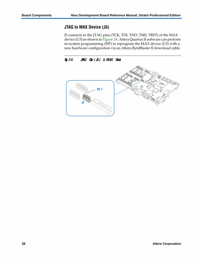
JTAG to MAX Device (J5)
J5 connects to the JTAG pins (TCK, TDI, TDO, TMS, TRST) of the MAX device (U3) as shown in Figure 24. Altera Quartus II software can perform in-system programming (ISP) to reprogram the MAX device (U3) with a new hardware configuration via an Altera ByteBlaster II download cable.
Figure 24. JTAG Connector (J5) to MAX Device
J5
Pin 1
38 Altera Corporation

Appendix A
2
Appendix A: Shared Bus Table
On the Nios Development Board, Stratix Edition, the flash memory, SRAM and Ethernet MAC/PHY devices share address and control lines. These shared lines are referred to as the Shared Bus. Using SOPC Builder, designers can interface a Nios processor system to any device connected to the off-chip shared bus.
Table 9 on page 40 lists all connections between the devices connected to the shared bus.
Altera Corporation 39

Shared Bus Table Nios Development Board Reference Manual, Stratix Professional Edition
.
Table 9. Shared Bus Table (Part 1 of 3)
NET Name NETDescription
PLD (U53) Flash (U5) SRAM (U35) SRAM (U36) Ethernet (U4)
Pin Name
Pin # Pin Name
Pin # Pin Name
Pin # Pin Name
Pin # Pin Name Pin #
FSE_A0 Shared Address
IO A4 A0 27
FSE_A1 IO A3 A1 22 A1 78
FSE_A2 IO B3 A2 21 A0 1 A0 1 A2 79
FSE_A3 IO B5 A3 20 A1 2 A1 2 A3 80
FSE_A4 IO B4 A4 19 A2 3 A2 3 A4 81
FSE_A5 IO C4 A5 18 A3 4 A3 4 A5 82
FSE_A6 IO A5 A6 17 A4 5 A4 5 A6 83
FSE_A7 IO C5 A7 16 A5 18 A5 18 A7 84
FSE_A8 IO D5 A8 10 A6 19 A6 19 A8 85
FSE_A9 IO E6 A9 9 A7 20 A7 20 A9 86
FSE_A10 IO A6 A10 42 A8 21 A8 21 A10 87
FSE_A11 IO B7 A11 8 A9 22 A9 22 A11 88
FSE_A12 IO D6 A12 7 A10 23 A10 23 A12 89
FSE_A13 IO A7 A13 6 A11 24 A11 24 A13 90
FSE_A14 IO D7 A14 5 A12 25 A12 25 A14 91
FSE_A15 IO C6 A15 4 A13 26 A13 26 A15 92
FSE_A16 IO C7 A16 3 A14 27 A14 27
FSE_A17 IO B6 A17 46 A15 42 A15 42
FSE_A18 IO D8 A18 15 A16 43 A16 43
FSE_A19 IO C8 A19 43 A17 44 A17 44
FSE_A20 IO E8 A20 44
FSE_A21 IO D9 A21 35
FSE_A22 IO B9 A22 2
40 Altera Corporation

Nios Development Board Reference Manual, Stratix Professional Edition Shared Bus Table
Appendix A
2
FSE_D0 Shared Data IO H12 D0 31 D0 7 D0 107
FSE_D1 IO F12 D1 32 D1 8 D1 106
FSE_D2 IO J12 D2 33 D2 9 D2 105
FSE_D3 IO M12 D3 34 D3 10 D3 104
FSE_D4 IO H17 D4 38 D4 13 D4 102
FSE_D5 IO K18 D5 39 D5 14 D5 101
FSE_D6 IO H18 D6 40 D6 15 D6 100
FSE_D7 IO G18 D7 41 D7 16 D7 99
FSE_D8 IO B8 D8 29 D8 76
FSE_D9 IO A8 D9 30 D9 75
FSE_D10 IO A9 D10 31 D10 74
FSE_D11 IO C9 D11 32 D11 73
FSE_D12 IO E10 D12 35 D12 71
FSE_D13 IO A10 D13 36 D13 70
FSE_D14 IO C10 D14 37 D14 69
FSE_D15 IO B10 D15 38 D15 68
FSE_D16 IO A11 D0 7 D16 66
FSE_D17 IO C11 D1 8 D17 65
FSE_D18 IO D11 D2 9 D18 64
FSE_D19 IO B11 D3 10 D19 63
FSE_D20 IO D10 D4 13 D20 61
FSE_D21 IO G10 D5 14 D21 60
FSE_D22 IO F10 D6 15 D22 59
FSE_D23 IO H11 D7 16 D23 58
FSE_D24 IO G11 D8 29 D24 56
FSE_D25 IO F8 D9 30 D25 55
FSE_D26 IO J9 D10 31 D26 54
FSE_D27 IO J13 D11 32 D27 53
FSE_D28 IO L13 D12 35 D28 51
FSE_D29 IO M11 D13 36 D29 50
FSE_D30 IO L11 D14 37 D30 49
FSE_D31 IO G7 D15 38 D31 48
Table 9. Shared Bus Table (Part 2 of 3)
NET Name NETDescription
PLD (U53) Flash (U5) SRAM (U35) SRAM (U36) Ethernet (U4)
Altera Corporation 41

Shared Bus Table Nios Development Board Reference Manual, Stratix Professional Edition
FLASH_CS_n Chip Select IO K19 CE_n 28
FLASH_OE-N Read Enable IO F19 OE_n 30
FLASH_RW-N Write Enable IO G19 WE_n 11
FLASH_RY-BY_N Ready/Busy IO L18 RY/BY_n 14
SRAM_BE_N0 Byte Enable 0 IO M18 BE0# 39
SRAM_BE_N1 Byte Enable 1 IO F17 BE1# 40
SRAM_BE_N2 Byte Enable 2 IO J18 BE2# 39
SRAM_BE_N3 Byte Enable 3 IO L17 BE3# 40
SRAM_CS_N Chip Select IO B24 CS_n 6 CS_n 6
SRAM_OE_N Read Enable IO B26 OE_n 41 OE_n 41
SRAM_WE_N Write Enable IO C24 WE_n 17 WE_n 17
ENET_ADS_N Address Strobe IO V25 ADS# 37
ENET_AEN Address Enable IO V28 AEN 41
ENET_BE_N0 Byte Enable 0 IO T22 BE0# 94
ENET_BE_N1 Byte Enable 1 IO U26 BE1# 95
ENET_BE_N2 Byte Enable 2 IO U25 BE2# 96
ENET_BE_N3 Byte Enable 3 IO T19 BE3# 97
ENET_CYCLE_N Bus Cycle IO U27 CYCLE# 35
ENET_DATACS_N Data Chip Select
IO T20 DATACS# 34
ENET_INTRQ0 Interrupt IO V27 INTRO 29
ENET_IOCHRDY IO Char Ready IO V26 ARDY 38
ENET_IOR_N Read IO T23 RD# 31
ENET_IOW_N Write IO T24 WR# 32
ENET_LCLK Local Bus Clock
IO R26 LCLK 42
ENET_LDEV_N Local Device IO T26 LDEV# 45
ENET_RDYRTN_N Ready Return IO T28 RDYRTN# 46
ENET_W_R_N Write/Read IO T21 W/R# 36
Table 9. Shared Bus Table (Part 3 of 3)
NET Name NETDescription
PLD (U53) Flash (U5) SRAM (U35) SRAM (U36) Ethernet (U4)
42 Altera Corporation

Appendix B
3
Appendix B: Restore the Factory Configuration
The Nios development board can always be restored to its factory-programmed configuration. To restore the factory configuration, you must reprogram the flash memory on the Nios development board.
Reprogramming the flash memory requires the following:
■ A Nios processor hardware design configured in the Stratix device and executing the GERMS monitor.
■ The factory flash image for GERMS to program into the flash memory.
Configuring the Stratix Device
With the above mentioned requirements, perform the following steps:
1. Connect the Nios development board to the host computer using the ByteBlaster II download cable.
2. Launch the Quartus II software and open the Programmer window (Tools menu).
3. Click Add File... and select the following configuration file:
<Nios Development Kit <install directory> /examples/recovery_configuration_stratix_1s40.sof
4. In the Programmer window, check the Program/Configure box, and click Start to download the hardware configuration.
5. After configuration completes, hold down SW0, press and release SW8 and then release SW0.
The Stratix device is configured with a Nios processor hardware design executing the GERMS monitor. At this stage, DO NOT push the Safe Config or Reset, Config buttons, because it will reset the Stratix configuration.
f See the Nios Hardware Development Tutorial for a detailed description of configuring the Stratix device using the Quartus II software.
Altera Corporation 43

Restore the Factory Configuration Nios Development Board Reference Manual, Stratix Professional
Reprogramming the Flash Memory
You can now use the Nios processor in the Stratix device and the GERMS monitor to reprogram the flash memory by performing the following steps:
1. Connect the Console RS-232 serial connector to the host computer using a serial cable.
2. Open a Nios SDK Shell by choosing Programs > Altera > Nios Development Kit <installed version> Nios SDK Shell (Start menu). The default flash image file is located in the Nios SDK Shell default directory.
3. To download the flash file to the GERMS monitor executing on the board, type:
nios-run -x -r -p com1 default_board_image_stratix_1s40.flash
This command assumes the you connected the serial cable to COM1 on your host computer. If you are using a different COM port, change the com1 argument appropriately.
4. It will take 10 to 20 minutes to download the entire flash image. Do not reset the board during this time. When the download is complete, the Nios SDK Shell will return to a bash prompt.
5. Push the Safe Config button to perform a power-on reset and reconfigure the Stratix device from flash memory. You should see the Safe LED turned on and activity on LEDs D0 — D7.
Your board is now re-configured to the default factory condition.
44 Altera Corporation
Appendix C
4
Appendix C: Board Ethernet Connection
The default reference design shipped on the Nios development board implements a web server, among other functions. The Ethernet port provides a very fast and easy method to download hardware and software images to the board via a web browser on your host computer. The software reference design implements a web server on the Ethernet port as soon as the board powers up and configures with the factory-programmed safe configuration. The web server responds to any HTTP requests, regardless of origin, that arrive on its Ethernet connection.
This section assumes that you are familiar with the Nios SDK shell, the nios-run utility for serial communication with the Nios development board, and the GERMS monitor.
f See the Nios Embedded Processor Software Development Reference Manual for information on these topics.
Connecting the Ethernet Cable
The Nios Development Kit includes an Ethernet (RJ45) cable and a male/female RJ45 crossover adapter. Before you connect these components, you must decide how you want to use the network features of your board. Select one of the two following connection methods:
1. Point-to-Point Connection — To use your Nios Development Board connected directly to a host computer point-to-point (not on a LAN), do the following:
a. Connect one end of your RJ45 cable to the female socket in the crossover adapter.
b. Insert the male end of the crossover adapter into RJ1 on the Nios Development Board.
c. Connect the other end of the RJ45 connector directly to the network (Ethernet) port on your host computer (see Figure 25).
Altera Corporation 45

Board Ethernet Connection Nios Development Board Reference Manual, Stratix Professional Edition
Figure 25. Point-to-Point Connection
2. LAN Connection — To use your Nios development board on a LAN (for example, connecting to an Ethernet hub) do the following:
a. Connect one end of the RJ45 cable to the Ethernet connector on the development board (RJ1).
b. Connect the other end to your LAN connection (hub, router, wall plug, etc.).
Connecting the LCD Display
Your Nios Development Kit was delivered with a two-line x 16-character LCD text display. The web-server software displays useful status and progress messages on this display. If you wish to use the network features of the board, connect the LCD display to the Expansion Prototype Header J12 as shown in Figure 26 (take special care of the location of pin 1).
Figure 26. Expansion Prototype Header - J12
Obtaining an IP address: DHCP
In order to function on a network (either a point–to–point or LAN), your board must have an IP address. Upon reset, the web server will attempt to acquire an IP address via the DHCP protocol. Many LANs support DHCP.
1 If you do not know whether or not your LAN supports DHCP, it’s probably best to try DHCP first.
46 Altera Corporation

Nios Development Board Reference Manual, Stratix Professional Edition Board Ethernet Connection
Appendix C
4
The board will continue to attempt DHCP self-configuration for one full minute. You can tell whether DHCP has succeeded, or is still in progress, by reading status messages on the LCD display. If your LAN does not support DHCP, or if you are using the point-to-point option above, then DHCP configuration will ultimately fail.
You can stop the DHCP process at any time by pressing push button switch SW3. Sending an exclamation point (!) to the board on the console serial port will also immediately terminate DHCP configuration.
If DHCP succeeds, the board will display a success message on the LCD display. It will also continuously display its IP address.
If DHCP fails (or is aborted), the board will obtain its IP address from flash memory. All boards are delivered from the factory with the IP address 10.0.0.51. You can change the IP address using commands sent via the console serial port (see “IP Addresses for Point–to–Point Connections” below.)
IP Addresses for Point–to–Point Connections
Your host computer and the development board are the only two devices connected to a very simple (one-wire) network. When the board is delivered from the factory, it is pre-programmed with the default IP address 10.0.0.51. (The 10.0.0.x subnet is conventionally reserved for development, testing, and prototyping). For most operating systems, it will be necessary to assign your host computer an IP address on this same subnet.
For example, the address 10.0.0.1 will work fine. Your computer and your development board are the only two devices connected on this simple network, so it is not necessary to get an address assigned to you by your system administrator. Any address in the 10.0.0.x subnet will work and there is no possibility of conflicting with another device on the network. You do, however, need the ability to change the IP address of your host computer. On Windows machines, this is accomplished through the Network Connections control panel.
Upon reset, the board will power up and attempt DHCP self-configuration. On a point–to–point network, you should abort DHCP by pressing SW3. If you frequently use your board in a point–to–point configuration, you may wish to disable DHCP entirely by typing the command: xdhcp:off to the console serial port.
Altera Corporation 47

Board Ethernet Connection Nios Development Board Reference Manual, Stratix Professional Edition
IP Addresses for LAN Connections
If your LAN does not support DHCP, or if DHCP self-configuration failed, then you will need to assign your board a fixed IP address before you can access it over a network. All boards arrive with a default IP address of 10.0.0.51. (The 10.0.0.x subnet is conventionally reserved for development, test, and prototyping). You need to obtain a safe IP address in your LAN's subnet from your system administrator.
Once you have obtained a safe IP address, you can assign it to your board using GERMS commands over the serial connection. The GERMS monitor in the default software reference design is extended to implement the xip command. The xip command sets the IP address for your board, and saves this address in flash memory. In general, you will only need to assign an IP address to your board once. However, you may change it at any time by issuing another xip command.
For example, to assign the IP address 137.57.136.165, type the following command at the GERMS + prompt:
xip:137.57.136.165 (no spaces)
1 The GERMS monitor does not recognize the Backspace key or Delete key. If you make a mistake typing, press the Escape key to get a fresh GERMS prompt and re-enter the command. To read back the IP address, you can use the xip command with no colon or arguments. To activate the new IP address, you must reset your board by pushing the Safe Config button or the Reset, Config button.
Browsing your Board
Once your board has a valid IP address (obtained from either DHCP self-configuration or from flash memory), you can access the board via a web browser (e.g., Microsoft Internet Explorer). The board serves a website which includes both extensive documentation and useful network-download utility functions. To browse this site, open a web browser and type the IP address of the board (four numbers separated by decimal-points) as a URL directly into the browser’s Address input field. You can determine your board’s IP address by reading the messages displayed on the LCD display (the IP address is continuously displayed) or by typing xip on the Console Serial Port.
f Extensive additional information on the board’s network communications and download utilities are available via this web interface.
48 Altera Corporation

Index
5
Index
A
Appendix AShared bus table 39
Appendix BRestore the factory configuration 43
Appendix CBoard Ethernet connection 45
B
Block diagram 11Board Ethernet connection
Browse the board 48Connecting the Ethernet cable 45Connecting the LCD display 46Obtaining an IP address - DHCP 46
LAN connections 48Point-to-point connections 47
C
Clock circuitry 35Compact flash connector 14Configuration and reset buttons 34
SW10 - Reset config 34SW8 - CPU reset 34SW9 - Safe config 34
Configuration controller device 27Configuration data 28Configuration-status LEDs 33
Indicators 33Reset distribution 27Safe and user configurations 29Starting configuration 28Stratix configuration 28
Conventional flash memory usage 29
D
Development boardComponent illustration 12Features 9General description 9
Dual 7-segment display 26U8 & U9 pin information 26
E
Ethernet PHY/MAC 19Expansion connector header
pin out information 20Expansion connector header (PROTO1) 19
J11 pin information 20J12 pin information 21J13 pin information 21
Expansion connector header (PROTO2) 21J15 pin information 23J16 pin information 22J17 pin information 23
F
Flash memory allocation 30Flash memory device 13
I
Individual LEDs (D0 - D7) 27pin information 27
J
JTAG connections 36JTAG to MAX device (J5) 38JTAG to Stratix device (J24) 36, 38
Altera Corporation 49

Index Nios Development Board, Stratix Professional Edition Reference Manual
M
Mictor connector 23Debug port to OCI debug module 24J25 pin information 25
P
Power-supply circuitry 35Push-button switches 27
pin information 27
R
Reference designdefault 9restoring 10
Restore factory configurationConfiguring the Stratix device 43Reprogramming flash memory 44
S
Safe hardware configuration dataMemory allocation 32
Schematics 12SDRAM device 16Serial port connectors 25
ConsoleJ19 pin information 26
DebugJ27 pin information 26
SRAM devices 18Stratix 1S40 device 13SW10 button 34SW8 button 34SW9 button 34
50 Altera Corporation