
Semiconductor Devices -- not only to understand what were invented, but also be able create your own...
46
Semiconductor Devices -- not only to understand what were invented, but also be able create your own -- Kai Shum 2011-12-02
-
date post
20-Dec-2015 -
Category
Documents
-
view
214 -
download
0
Transcript of Semiconductor Devices -- not only to understand what were invented, but also be able create your own...

Semiconductor Devices-- not only to understand what were invented, but
also be able create your own --
Kai Shum2011-12-02

How?
• Books tell you how to understand the operation principles for devices already invented
• Not only understanding• But also to teach you how to invent your own
devices by exploring new physical processes in semiconductors

Summary for invented devicesName Key Structure Comment
Diode pn Basic unit
Bipolar Junction Transistor (BJT)
pn 2 units
Electric-field Effect Transistor(MOSFET)
MOS Basic unit – e-to-e
Light-emitting Diode (LED) pn Positively biased
Laser Diode (LD) pn Positively biased
Modulator pn Negatively biased
Electro-absorption Modulated Laser (EML)
pn 1 unit p-biased and 2nd unit n-biased
Charge-Coupled Device (CCD) MOS Basic unit – o-to-e
Solar Cell pn Generating photo-voltage, photo-current

Basic device units
• PN Junction• MOS (or MIS)

A few basic concepts
• Fermi level• Contacts• Build-in electric field

Fermi level
• Fermi level is a reference potential energy level that detects the single particle electron occupation probability in a semiconductor or dissimilar semiconductors in physical contact at equilibrium (e obey Fermi-D distribution)
• Example, at the exact Fermi energy level, the probability for an electron to occupy at this energy level is 50%

Example 1: Intrinsic Semiconductor at 0 K

Example 2: Intrinsic Semiconductor at 300 K
- --
-
+
+
+ +

Example 1: Doped Semiconductors
N-type P-type

Example 1: Doped Semiconductors
N-type P-type

Fermi-Energy
• The Fermi energy is a concept in quantum mechanics usually referring to the energy of the highest occupied quantum state in a system of fermions at absolute zero temperature.
http://en.wikipedia.org/wiki/Fermi_energy
See a nice description on Wiki:

Contacts
• Contacts are terminals used to accept external potentials and to a complete circuit

Different type of contacts
• ohmic contact• Schottky contact

Schottky contact

Schottky contact

Ohmic contact

Biased contacts

Tunneling ohm contact

Schottky contact

PN Junction

Pn junction, 0, +, and - biased

Majority carriers in pn junction

I-V curve of pn diode

MOS (or MIS)

MOS, negatively biased

MOS positively biased

MOSFET action


CCD


-


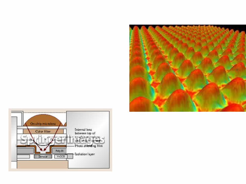

Fast color CCD

CCD Inventor

Solar cells


Intra-band & inter-band tunneling

Resonant tunneling

To be continued on modulators, EMLs, LEDs, LDs


![Beli Shum u Shumi [Oc]r](https://static.fdocuments.net/doc/165x107/577cc0e11a28aba71191724e/beli-shum-u-shumi-ocr.jpg)