Sander Mos / Martin van Beuzekom 17 January 20061 PRR of Pile-Up Hybrid Outline: Introduction Hybrid...
32
17 January 2006 1 Sander Mos / Martin van Beuzekom PRR of Pile-Up Hybrid Outline: • Introduction • Hybrid design • Test results • Production • Conclusion / Timeline
-
Upload
suzanna-newman -
Category
Documents
-
view
213 -
download
0
Transcript of Sander Mos / Martin van Beuzekom 17 January 20061 PRR of Pile-Up Hybrid Outline: Introduction Hybrid...

17 January 2006 1 Sander Mos / Martin van Beuzekom
PRR of Pile-Up Hybrid
Outline:• Introduction• Hybrid design• Test results• Production• Conclusion / Timeline

17 January 2006 2 Sander Mos / Martin van Beuzekom
General
• Some initial remarks– We only need 4+2 complete hybrids– The layout of the hybrid is a compromise in several
aspects• Characteristic impedance• Analog signals of the pile-up are in the first place used to
check the performance on the comparators– Concerning the production of the module (not only
hybrid) we lean heavily on the experience from the Liverpool group
• We do not have the manpower/budget to make many prototypes/tests
– Module / silicon precision less stringent than for VELO• Several tens of micrometers accuracy is enough

17 January 2006 3 Sander Mos / Martin van Beuzekom
Overview Vertex Locator
4 Pile-Up modules
R sensors only

17 January 2006 4 Sander Mos / Martin van Beuzekom
Module
• The hybrid will be glued to a Carbon fiber substrate supplied by Liverpool / Stevenage.• Module pedestal same as VELO, also supplied by Liverpool•Module construction done by NIKHEF
Pile-Up modules:1. Silicon sensor2. kapton flex circuit laminated
onto 3. carbon fibre/ TPG composite4. cooling cookies 5. low mass carbon fibre paddle6. precision aluminium base
plate

17 January 2006 5 Sander Mos / Martin van Beuzekom
Electrical connections
• 4 times # connections per hybrid than VELO
– 4 cable sets needed– 2 layers of hybrid tails
Solder maskCopperPolyimideStiffener
Hybrid Side View

17 January 2006 6 Sander Mos / Martin van Beuzekom
Hybrid design

17 January 2006 7 Sander Mos / Martin van Beuzekom
Hybrid Design
General:• 8 Layer flex-rigid polyimide (Kapton)• Dimensions 492 x 180 mm• Smallest track / gap : 50µm / 50µm (top) 100µm / 100µm
(inner)• Tails are part of the hybrid
Electrical:• 16 beetle chips fully connected
• Controlled (differential) impedance stripline, Z0 -> 66
• 64 analog & 256 digital - differential pairs• 1 ground plane + split power planes (split supply)• More than 320µF decoupling on power supply• Bias scheme and control identical to VELO

17 January 2006 8 Sander Mos / Martin van Beuzekom
Hybrid Design (2)
Pitch adaptors:• Separate design• Single layer• 17µm track and gap• Produced at CERN• Available !
Thermal:• Vias round the Beetles thermally connect top to bottom layer• The top ground plane below the pitch adapters and the silicon is thermally isolated from the beetles.

17 January 2006 9 Sander Mos / Martin van Beuzekom
Pile-Up Hybrid
17 January 2006 10 Sander Mos / Martin van Beuzekom
Comparison Pile-Up <-> VELO
Electrical:• 256 LVDS signals @80Mbit/s in addition to 64 analog signals• per tail twice the number of tracks • Analog readout and control identical to VELO• Analog outputs are less important• Differential impedance : 66Ω
– Mismatch w.r.t. long kapton cables (80Ω)– no solution for impedance mismatch
Mechanical:• Tails are part of the hybrid• Split tails• CF-TPG-substrate is the same as the VELO except that the
Pile-Up is 5mm wider.• Only one hybrid per module (asymmetry)

17 January 2006 11 Sander Mos / Martin van Beuzekom
PrototypesDesign/manufacturing History• 2001 : design of VELO hybrid (Beetle 1.1)
– Needed for Beetle/SCTA decision– Good exercise for the Pile-Up hybrid– Produced in industry, 2 companies failed, only 75µm tracks
• 2002 : first design of Pile-Up hybrid (Beetle 1.2)– Cannot be made in industry, CERN offered outcome– Unfortunately production failed after long time/many attempts
• 2004 : redesign/production of prototype Pile-Up hybrid (Beetle 1.3/1.4)
– Significant design changes -> connectors to backside of tails– Improvements to ease production– CERN PCB lab. Produced 1 - 2 prototypes
• 2005 : Hybrid assembled and tested– silicon sensor arrived in July/August (200µm instead of 300µm)– Final Hybrid is designed -> subject of this PRR
Additional obstacles:• CAD software : Beetle placement / routing problem
– Special software (c++) was written to rotate all the parts to the correct angle
– Also a program was made to generate the complete pitch adapters• Split tails• Pr04 silicon sensor is mirrored -> redesign of pitch adapters

17 January 2006 12 Sander Mos / Martin van Beuzekom
Test results

17 January 2006 13 Sander Mos / Martin van Beuzekom
Hybrid test setup
Test setup:• 5 delay circuits with 10ps step 12 bit -> 40 ns variable delay
– Beetle Testpulse, Beetle Trigger, Beetle Clock, ADC Clock, ADC Trigger
• 2 analog 16 channel differential amplifier boards• VME crate with:
- UTB (universal test board) 256 differential LVDS inputs, per channel 2 kbit fifo, running at 80 MHz.- 8 channel differential ADC (40MHz).
• Windows pc with Labview for I2C and delay control• Linux pc for control of VME and DAQ + Labview by TCP
connection.• Cooling: hybrid is placed on a heatsink with fan
17 January 2006 14 Sander Mos / Martin van Beuzekom
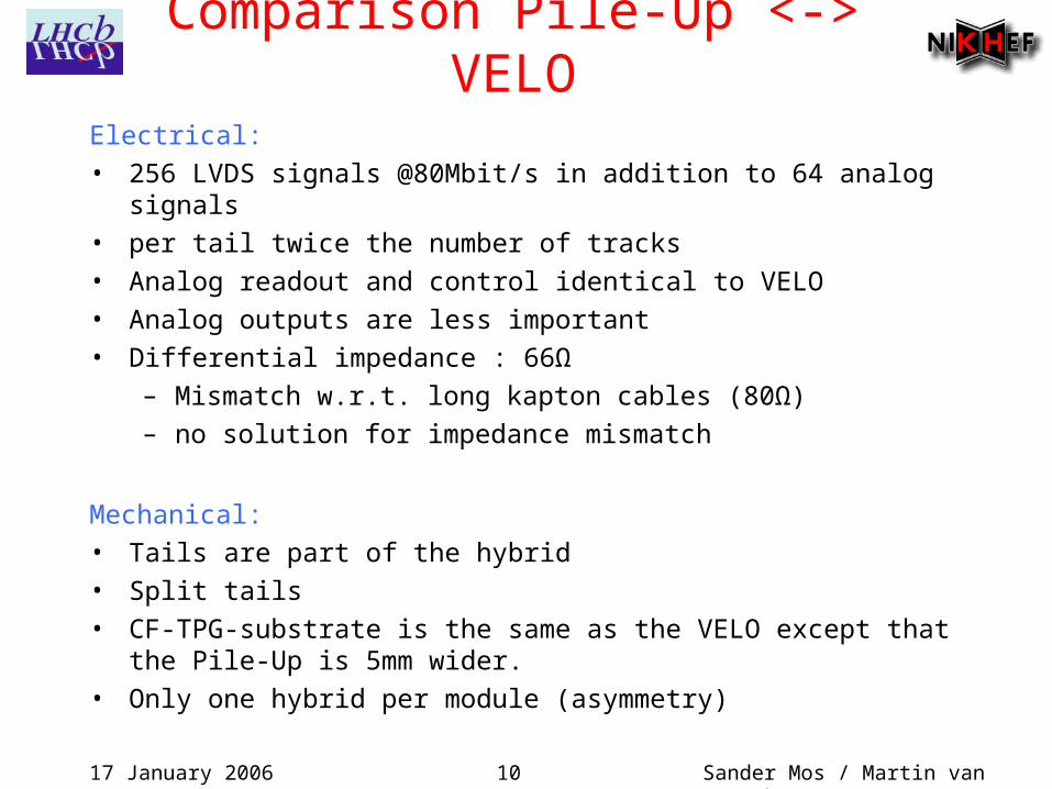
Prototype testsGeneral• Large “parameter space” to explore in the crosstalk tests
– With/without analog readout– With/without triggers– With/without silicon– Analog vs. comparator clock timing– # channels (test) pulsing 1/2/4/8/16/32/64– Single chip/2chips/4/8/16 + many permutations
• Line driving capability of LVDS outputs checked with 20 meter long cat6 cable
Without silicon, crosstalk tests• Analog -> digital crosstalk
– internal in chip• also seen in tests with Heidelberg daughterboard (1/2beetles)
– even present when the analog outputs are switched off

17 January 2006 15 Sander Mos / Martin van Beuzekom
Prototype testsWithout silicon, crosstalk tests (continued)• Digital -> analog crosstalk
– only when a large number of channels (> 16/32) are simultaneously switching• Chip -> chip crosstalk
– power decoupling was not optimal– doubling the capacitance per chip gave improvement– further increase in capacitance proved useless– different powering schemes gave no further improvement
With silicon sensor (pr04)• Only a 200µm thick silicon sensor was available (300µm needed on final modules)
– Silicon showed high leakage current– Not resolved but likely due to sensor– High leakage current mode reported by Liverpool (LHCb week December
2005)• Tests done with shaper setting Vfs=500 mV • Chips connected to the inner short strips of the silicon showed better SNR then the
ones connected to the outer long strips– The outer strips have higher capacitance
• Radioactive (90Sr) source test done (no trigger, random sampling)– Polarity of signals from silicon and comparator verified to be OK– No opportunity for beam test

17 January 2006 16 Sander Mos / Martin van Beuzekom
Reminder : Threshold requirements
• Assumptions– 300 m thick silicon detectors => 22ke- per MIP– Minimum S/N = 10 – Strip occupancy 1 %
• Requirements for pile-up veto– 100 % efficiency (charge sharing, worst case: ½ of
signal on a strip)– Maximum contribution of noise hits: few %– Threshold step size better than 0.1 MIP
Optimal threshold = 0.4..0.5 Mip (9..11 ke-)

17 January 2006 17 Sander Mos / Martin van Beuzekom
Threshold 8 ke-Threshold 9 ke-Threshold 10 ke-Threshold 7 ke-
16 beetle chips x 32 comparator outputs
# H
its
Crosstalk from analog readout
Threshold requirement: 9..11ke-
Conclusion : crosstalk from analog readout is acceptable

17 January 2006 18 Sander Mos / Martin van Beuzekom
Threshold check
Threshold:9 ke-
8 ke-
Quiet forthreshold > 8 ke-

17 January 2006 19 Sander Mos / Martin van Beuzekom
Analog: noise behaviourN
ois
e [
a.u
.]
Beetle channels
4 chips x 4 channels switching 16 chips x 16 channels switching
Long strips
short strips
SNR = 15 .. 16No common mode noise correction
Conclusions:
• Noise depends somewhat on # channels switching• S/N according to expectation

17 January 2006 20 Sander Mos / Martin van Beuzekom
Connectivity errors#1 hybrid with beetles and silicon• 13 broken traces -> repaired 11 (CERN)• ?? Can be repaired on final hybrid ??
#2 bare circuit• Before 6 open & 1 short between 2 traces
- 3 near connector, 1 located 25% from connector, 1 located 25% from chip & 1 located 50% from chip
• Extreme thermal test (-40° +80°C) we tried to push it to/over the edge
• After thermal test
- 11 open & 20+ bad connections (bad = ΔR › 1Ω) & 1 short
- (almost) all on "left half" of hybrid and bottom tail
- cause: broken vias near chip, "long vias" only

17 January 2006 21 Sander Mos / Martin van Beuzekom
Connectivity errors : details
Many broken vias Solder mask
CopperPolyimideStiffener
Side View
• Optimist’s view : 3/4 of the vias survived the test!• what is the difference between left/right?- Question can we address this left/right difference in the next production round
10 open & 20+ (6 – 11Ω)
1 open & 1 short (also before thermal cycling)
500 mm
180
mm
110 mm 100 mm
right
left

17 January 2006 22 Sander Mos / Martin van Beuzekom
Thermal cycling #1• Thermal test +25° -25°C, 2 hour cycle, 10 cycles total• Aim of the test was to stress the hybrid (vias) not the
silicon• Unfortunately the silicon broke due to thermal stress
– Further investigation needed• Freezing of moisture?, glue problem?• Glue recipe will be copied from Liverpool for real module
– BUT, it is not a hybrid problem…

17 January 2006 23 Sander Mos / Martin van Beuzekom
Summary of results
• Electrical performance of the hybrid is good– Chip to chip crosstalk minimized by adding decoupling
cap’s– Design is close to optimal
• With this hybrid + beetle combination we can do physics!– Beetle offsets can be tuned to make “flat threshold”– Threshold can be put at 0.4 Mip. (~100% detection
efficiency)
• Connectivity is a point of concern– Broken traces (not via), but can be repaired– Vias failed during thermal cycling
• Problem of test?• Can we improve the via strength?

17 January 2006 24 Sander Mos / Martin van Beuzekom
Production

17 January 2006 25 Sander Mos / Martin van Beuzekom
Modifications for final design
• Split Vdd power plane– Hybrid current > Radhard regulator current– Parallel connection of regulators not possible (R.Frei)
-> split Vdd plane– Still one ground plane– Risk: moderate (VELO hybrid: no problem)
• Slots in tails for mounting of cooling screws– Rerouting of bulk of tracks– Risk: low, because same design rule (gap) is used
• Small modifications around the chips (1.3 ->1.5)• Extra fiducials for silicon alignment• Decreased length from 500 -> 492 mm
All layout modifications already implemented!

17 January 2006 26 Sander Mos / Martin van Beuzekom
Module ProductionProduction steps:• Gluing hybrid to substrate -> CERN ?
– CF-TPG substrate supplied by Liverpool /Stevenage• Assembly of connectors / passive components
– NIKHEF or specialized company• Bonding of chips @ NIKHEF
– control lines, analog + digital outputs– Tested Beetle chips 1.5 available
• Test– check programming/clocks/triggers/outputs– do threshold scan (to make sure that we picked the right Beetles)!
• Glue silicon and pitch adaptor & bonding– Silicon (300µm pr04, Liverpool)– Pitch adapter is NIKHEF design (available)
• Test : silicon -> Beetle bonds– Testpulse / radioactive source
• Pedestal assembly– follow Liverpool procedure
• Burn-in test– Similar to “Glasgow – Liverpool” procedure

17 January 2006 27 Sander Mos / Martin van Beuzekom
Conclusions / timeline
Summary / conclusions:• Many crosstalk tests done with & without silicon• Design close to optimum• Hybrid + silicon combination make up a working
detector– Performance is more limited by Beetle than by hybrid!
• Electrical connectivity needs attention in production– Can we offer help in testing during production?
• We judge the Pile-Up hybrid to be ready for production
Production timeline• Hybrid production 3 months?• Module production another 3 - 4 months
– Rely on experience from Liverpool• Modules should be ready by October 2006 !! (VELO
planning)• Production schedule is very tight!

17 January 2006 28 Sander Mos / Martin van Beuzekom
End

17 January 2006 29 Sander Mos / Martin van Beuzekom
Beetle selection• Wafer test in Heidelberg
– Heidelberg analog + logic test was extended with a comparator test – NIKHEF supplied the VHDL-code of the digital acquisition hardware
+ software for the comparator test (+ test in-situ)- tests: output mask / all comparator threshold DACs / Main threshold DAC– Analysis of comparator data is done by the NIKHEF group– So far 4 wafers tested (limited by time/availability of probe station)
• ~900 beetle1.4 and ~900 Beetle1.5 to select from– Plan to test all remaining (~15 wafers) with comparator test enabled
• Selecting chips:– Current preference is Beetle1.5 (mainly to be compatible with VELO)- Test yield > 70..80% (depending on wafer)
- But limitations of comparator test qualifies some chips as bad while OK -> real yield 80+%
- Hard rejection criteria for beetle chips to be used in the pile-up:- Poor analog performance (from Heidelberg test)- Bad output mask register- Bad bit in 5-bit threshold DAC
- Additional rejection criteria: (see also next page)- Too low / too high threshold slope- Too large offset range
- Final selection:- Automated selection of ~200 chips with smallest offset spread- Manual final selection to catch anomalously behaving chips that pass the cuts- Difficult to make reliable cuts (yield is a steep function of criteria)

17 January 2006 30 Sander Mos / Martin van Beuzekom
Threshold dac-value
Thre
shold
/ o
ffse
t (k
e-)
poor bad really bad
Threshold slope
offsetrange
Beetle selection (2)
17 January 2006 31 Sander Mos / Martin van Beuzekom

17 January 2006 32 Sander Mos / Martin van Beuzekom
Silicon & Beetles
• Beetle nr and strip position