
recent advances in Modulated Pulsed Power Magnetron...
11
JOM • June 2011 48 www.tms.org/jom.html Overview Recent Advances in Modulated Pulsed Power Magnetron Sputtering for Surface Engineering Structural, Functional, and Biological Thin Films Jianliang Lin, William D. Sproul, John J. Moore, Zhili Wu, Sabrina Lee, Roman Chistyakov, and Bassam Abraham How would you… …describe the overall significance of this paper? There is a great need to advance the magnetron sputtering technique to produce better coatings. The research work reviewed in this article has demonstrated that the new MPP magnetron sputtering technique provides a controlled low ion energy and high metallic ion flux plasma, that densifies the growing film, improves the adhesion, produces thicker coatings and increases conformal coverage at a high deposition rate without detrimental increases in stress and defects. …describe this work to a materials science and engineering professional with no experience in your technical specialty? This paper provides an overview of recent research on the new MPP magnetron sputtering technique, in terms of the plasma properties, the great improvements in the structure and properties of the hard tribological coatings, and the important advances in the high rate deposition of the high performance, thick, hard, tribological coatings on the order of 10–100 mm in thickness, which, up to now, has been very difficult to do with sputtering. …describe this work to a layperson? Depositing a metal or compound film on a component surface can significantly increase the life and performance of the component under various harsh working conditions. Magnetron sputtering is one of the most practical methods to deposit high quality films. Recent advances in the new MPP magnetron sputtering technique as reviewed in this paper have shown promising results for producing better films and the capability to develop new, competitive manufacturing methods and technologies that will generate economic and technological capital for the society. Over the past 10 years, the devel- opment of high-power pulsed magne- tron sputtering (HPPMS) has shown considerable potential in improving the quality of sputtered films by gen- erating a high degree of ionization of the sputtered species to achieve high plasma density by using pulsed, high peak target power for a short period of time. However, the early HPPMS tech- nique showed a significantly decreased deposition rate as compared to tradi- tional magnetron sputtering. Recently, an alternative HPPMS deposition technique known as modulated pulsed power (MPP) magnetron sputtering has been developed. This new sputter- ing technique is capable of producing a high ionization fraction of sputter target species and while at the same time achieving a high deposition rate. This paper is aimed at giving a review of recent advances in the MPP tech- nique in terms of the plasma proper- ties, the improvements in the structure and properties of the thin films, and the important advances in the high rate de- position of high quality thick coatings on the order of 20-100 μm in thickness. INTRODUCTION For forty years magnetron sputtering has dominated many industries, while technological evolution has brought various other sputtering and chemi- cal vapor deposition techniques into practice. The plasma generated in DC magnetron sputtering (DCMS) is char- acterized by low ion energies (1–10 eV) and low ion flux that are composed largely of gaseous ions with less than 5% metal ions. Cathodic arc evapora- tion (CAE) has been a primary compet- itor to sputtering over the past twenty years because of its high deposition rate, high metal ionization fraction (up to 90%) and high ion energy (10–200 eV). The intense plasma generated by CAE is its main advantage over mag- netron sputtering, but the generation of macroparticle defects impairs the quality and properties of the deposited film. In addition, the high ion energy can also lead to high stress and defect densities in the film and degrade the toughness and tribological properties of the deposited coatings. In recent years, high power pulsed magnetron sputtering (HPPMS) (also known as high power impulse magne- tron sputtering (HIPIMS)) 1–3 and mod- ulated pulsed power (MPP) magnetron sputtering techniques, 4–8 a variation of HPPMS, have shown great advan- tages as compared to the conventional magnetron sputtering techniques. The HPPMS technique, originally devel- oped by Kouznetsov and co-workers, 1 is aimed at generating a high degree of ionization of the sputtered species to achieve high plasma density using a pulsed, high peak target power density for a short period of time. In HPPMS, the average thermal load on the target is kept low by operating the target with a high peak power density (e.g. 1–3 kWcm –2 ) for a short period of time (e.g. 100 ms) and a low duty cycle (1–10%). A considerably larger fraction of ion- ized species can be created by the high probability for ionizing collisions be- tween the sputtered atoms and ener- getic electrons. Investigations have recently been conducted to study the HPPMS plasma properties for different target materi- als. 9–14 It was found that the degree of ionization is strongly affected by the peak pulse power and the target material. It has been reported that the fraction of ionized target species in HPPMS can be increased up to 70%
Transcript of recent advances in Modulated Pulsed Power Magnetron...

JOM • June 201148 www.tms.org/jom.html
Overview
recent advances in Modulated Pulsed Power Magnetron sputtering for surface engineering
structural, functional, and Biological thin films
Jianliang Lin, William D. Sproul, John J. Moore, Zhili Wu, Sabrina Lee, Roman Chistyakov, and Bassam Abraham
How would you……describe the overall signifi cance of this paper?There is a great need to advance the magnetron sputtering technique to produce better coatings. The research work reviewed in this article has demonstrated that the new MPP magnetron sputtering technique provides a controlled low ion energy and high metallic ion fl ux plasma, that densifi es the growing fi lm, improves the adhesion, produces thicker coatings and increases conformal coverage at a high deposition rate without detrimental increases in stress and defects.
…describe this work to a materials science and engineering professional with no experience in your technical specialty?This paper provides an overview of recent research on the new MPP magnetron sputtering technique, in terms of the plasma properties, the great improvements in the structure and properties of the hard tribological coatings, and the important advances in the high rate deposition of the high performance, thick, hard, tribological coatings on the order of 10–100 mm in thickness, which, up to now, has been very diffi cult to do with sputtering.
…describe this work to a layperson?Depositing a metal or compound fi lm on a component surface can signifi cantly increase the life and performance of the component under various harsh working conditions. Magnetron sputtering is one of the most practical methods to deposit high quality fi lms. Recent advances in the new MPP magnetron sputtering technique as reviewed in this paper have shown promising results for producing better fi lms and the capability to develop new, competitive manufacturing methods and technologies that will generate economic and technological capital for the society.
Over the past 10 years, the devel-opment of high-power pulsed magne-tron sputtering (HPPMS) has shown considerable potential in improving the quality of sputtered fi lms by gen-erating a high degree of ionization of the sputtered species to achieve high plasma density by using pulsed, high peak target power for a short period of time. However, the early HPPMS tech-nique showed a signifi cantly decreased deposition rate as compared to tradi-tional magnetron sputtering. Recently, an alternative HPPMS deposition technique known as modulated pulsed power (MPP) magnetron sputtering has been developed. This new sputter-ing technique is capable of producing a high ionization fraction of sputter target species and while at the same time achieving a high deposition rate. This paper is aimed at giving a review of recent advances in the MPP tech-nique in terms of the plasma proper-ties, the improvements in the structure and properties of the thin fi lms, and the important advances in the high rate de-position of high quality thick coatings on the order of 20-100 μm in thickness.
introduction
For forty years magnetron sputtering has dominated many industries, while technological evolution has brought various other sputtering and chemi-cal vapor deposition techniques into practice. The plasma generated in DC magnetron sputtering (DCMS) is char-acterized by low ion energies (1–10 eV) and low ion fl ux that are composed largely of gaseous ions with less than 5% metal ions. Cathodic arc evapora-tion (CAE) has been a primary compet-itor to sputtering over the past twenty years because of its high deposition rate, high metal ionization fraction (up
to 90%) and high ion energy (10–200 eV). The intense plasma generated by CAE is its main advantage over mag-netron sputtering, but the generation of macroparticle defects impairs the quality and properties of the deposited fi lm. In addition, the high ion energy can also lead to high stress and defect densities in the fi lm and degrade the toughness and tribological properties of the deposited coatings. In recent years, high power pulsed magnetron sputtering (HPPMS) (also known as high power impulse magne-tron sputtering (HIPIMS))1–3 and mod-ulated pulsed power (MPP) magnetron sputtering techniques,4–8 a variation of HPPMS, have shown great advan-tages as compared to the conventional magnetron sputtering techniques. The HPPMS technique, originally devel-oped by Kouznetsov and co-workers,1 is aimed at generating a high degree of ionization of the sputtered species to achieve high plasma density using a pulsed, high peak target power density for a short period of time. In HPPMS, the average thermal load on the target is kept low by operating the target with a high peak power density (e.g. 1–3 kWcm–2) for a short period of time (e.g. 100 ms) and a low duty cycle (1–10%). A considerably larger fraction of ion-ized species can be created by the high probability for ionizing collisions be-tween the sputtered atoms and ener-getic electrons. Investigations have recently been conducted to study the HPPMS plasma properties for different target materi-als.9–14 It was found that the degree of ionization is strongly affected by the peak pulse power and the target material. It has been reported that the fraction of ionized target species in HPPMS can be increased up to 70%

Vol. 63 No. 6 • JOM 49www.tms.org/jom.html
or higher for Cu and Ti.11,12 Significant improvements in coating structure and properties,15–20 uniform deposition,21,22 and enhanced coating adhesion23,24 us-ing HIPIMS have been reported. How-ever, the much lower deposition rate of HPPMS compared to DCMS became a significant hindrance for industrial ap-plications.6,11,25–27 As summarized in a recent review by Sarakinos et al.,26 the HPPMS to DCMS deposition rate ra-tios for Ti is in a range of 15–75%, for Cr is 29%, for Cu is 37–80%, for Al is 35%, for Ta is 20–40%, for Zr is 15%, and for Al2O3 is 25–31%.6,25,26 The de-creased deposition rate in HPPMS has been explained mainly in that the ions can be attracted back toward the target and captured by the negative potential on the cathode as proposed in the mod-
el developed by Christie.28,29
As an alternative HPPMS technique, MPP has been developed by Chistya-kov and co-workers, and it overcomes the rate loss problem while still achiev-ing a high degree of ionization of the sputtered material.4,5 The difference between the originally introduced ver-sion of HPPMS by Kouznetsov and the MPP technique is basically in the mag-nitude, duration, and shape of the high power pulses. As shown in Figure 1, with the Kouznetsov technique, a sin-gle short high power pulse, on the order of 100–150 ms in duration is applied to the sputtering cathode, and the magni-tude of the pulse power density is on the order of 1.0 to 3.0 kWcm–2 (peak power can be in the low MW range de-pending on the sputtering target size) in
order to achieve a high degree of ion-ization of the sputtered material. With the MPP technique, the pulse length can be as long as 3,000 ms, and the peak power density is typically in the 0.5 to 1.5 kW/cm2 range. In MPP, the maximum duty cycle is 28% and the pulse frequency can be selected to be between 4 and 400 Hz. The most important feature of the MPP technique is that the MPP pulse shape can be arbitrarily tailored into a multistep pulse. Figure 2 shows the tar-get power, voltage, and current wave-forms during one typical MPP pulse pe-riod (the voltage values are negative).8 Unlike the simple one pulse shape in HPPMS, MPP generates a high density metal ion plasma by first producing a weakly ionized plasma followed by a transition to a strongly ionized plasma within one overall pulse. The weak ionization pulse segment is used to ignite an initial stable discharge with low power and current (steps 1 and 2 in Figure 2). Then a strong ionization pulse segment is generated with high power and current on the target as the main ionization stage (steps 3 and 4 in Figure 2). The control of the arbitrary pulse steps and shapes is achieved by controlling the voltage ‘on’ time (ton, the width of micro pulses) and the voltage ‘off’ time (toff, the distance be-tween micro pulses) within the micro pulse region (see the small insert graph on the right side in Figure 2). Given the capabilities to create multiple mi-cro pulse steps within one pulse and to adjust the power and current in each step, together with the arc suppression, stable deposition processes can be achieved in MPP for sputtering various metal films and for reactive sputter de-position of many compound materials.
MPP PlasMa characteristics
Recently, the time averaged ion mass distributions (IMD) and ion en-ergy distributions (IED) of the positive ions in the discharge plasmas during MPP magnetron sputtering of a Cr tar-get in pure Ar and Ar/N2 atmospheres have been determined using a Hiden electrostatic quadrupole plasma mass spectrometer (EQP) and compared with the plasma properties obtained us-ing DCMS and conventional pulsed dc
Figure 1. Typical target voltage waveforms and parameters of (a) HPPMS and (b) MPP.
a b
Typical HPPMS Pulse
Single-Pulse Time
Targ
et V
olta
ge
toff: the pulse off period (several ms)
ton: the pulse on period (100~150 ms)
Duty cycle: 1–10%Voltage: 800–1,000 VPeak Current: 100–300 APeak Power Density: 1–3 kW/cm2
Figure 2. Typical MPP pulse showing the target voltage, current, and power evolution dur-ing one modulated pulse (1.5 ms in this case): 1) ignition of the weakly ionized plasma; 2) duration of low power discharge; 3) transition stage from low power discharge to high power ionization discharge; 4) duration of the strongly ionization period. The inserted small curve on the right side shows the power supply generated micro-pulses within the strong ioniza-tion period with adjustable voltage on and off times (from Ref. 8 with permission, Elsevier).
The micro pulses within the pulse segments offer the flexibility to stabilize the plasma and control the voltage, current, and power.
0 500 1,000 1,500 2,000Time (ms)
900
800
700
600
500
400
300
200
100
0
Out
put V
alue
s (V
,A,k
W)
Weakly Ionized Plasma
Strongly Ionized Plasma
Voltage (negative)
Current
Power1 2
34
Typical MPP Pulse
Multi-Steps Time
toff: the pulse off period (several ms)
ton: the pulse on period (500~3000 ms)
Duty cycle: 10–28%Voltage: 700–800 VPeak Current: 100–300 APeak Power Density: 0.5–1.5 kW/cm2
Targ
et V
olta
ge

JOM • June 201150 www.tms.org/jom.html
magnetron sputtering (PMS) with simi-lar average target powers and deposi-tion conditions.8,30,31 In the pure Ar atmosphere condi-tions, the dominant ion species in a DCMS plasma are gas ions (Figure 3a). Significant increases in the number of both target material (Cr) and gas (Ar) ions for a MPP plasma compared to a DCMS plasma are demonstrated (Fig-ure 3b). Single and double ionized Cr and Ar ions were identified in the MPP plasma. The number of ions increased as the average target power (Pa) (as well as the peak power (Pp) and peak current (Ip)) was increased during the MPP sputtering. In the Ar/N2 mixture, the reactive gas (N2) was significantly ionized (N+ and N2
+) together with a large fraction of the metallic ion spe-cies, which could be beneficial for ob-taining stoichiometric compound films using a relatively lower partial pressure of the reactive gases (Figure 3c). The Cr+ IEDs in the plasmas gener-ated by DCMS, PMS and MPP tech-niques during reactive sputtering of CrN films are compared in Figure 4a. The other ion species exhibited a simi-lar IED shape but with slightly differ-ent maximum ion energies because of different ion masses. The IED curves were also plotted with a logarithmic scale and inserted in Figure 4a for the illustration of the existence of ions in the high energy range. Figure 4b de-picts the integrated Cr+, Ar+ and N+ ion fluxes in these plasmas. The IED of DCMS Cr+ ions (the solid square symbol) exhibits a peak energy of 4 eV and a maximum ion en-ergy of 15 eV in the tail (Figure 4a). The integrated ion fluxes in DCMS condition are low (Figure 4b). The numbers of Ar+ and N+ ions are much higher than that of Cr+ ions, suggesting that the major ion species in the DCMS plasma is from the gas, while the ion-ization degree of the metal target spe-cies is low. The IED of PMS Cr+ ions (the open circle) contains a wide range of energetic ions with a maximum en-ergy distribution extended above 100 eV (as shown in the curve plotted with the logarithmic scale). An increase in the number of Cr+, Ar+, and N+ ions was identified in the PMS plasma as com-pared to the DCMS condition (Figure 4b). However, similar to the DCMS
Figure 3. Ion mass distributions for (a) DCMS and (b) MPP of the Cr film depo-sitions, and for (c) MPP of the CrN film depositions (from Ref. 8 with permission, Elsevier).
a b
15 20 25 30 35 40 45 50 55 60m/e
8
6
4
2 Inte
nsity
x10
5 (CPS
)
3.0 kW
0.5 kW1.0 kW
1.5 kW2.0 kW
2.5 kW
p=0.5 kWp=1.0 kWp=1.5 kWp=2.0 kWp=2.5 kWp=3.0 kW
DC
40Ar+
52Cr+40Ar2+ 52Cr2+
15 20 25 30 35 40 45 50 55 60m/e
8
6
4
2
Inte
nsity
x10
5 (CPS
)
p=0.8 kWp=1.2 kWp=1.6 kWp=2.1 kWp=2.5 kWp=2.8 kW
MPP52Cr+40Ar+
52Cr2+40Ar2+
2.8 kW2.5 kW
2.1 kW1.6 kW
1.2 kW0.8 kW
c10N
10 20 30 40 50 60 70m/e
8
6
4
2
Inte
nsity
x10
5 (CPS
)
52Cr+
40Ar+
28N2+
14N+
52Cr2+
10% N220% N230% N240% N250% N260% N270% N2
70N60N
50N40N
30N20N
condition, the ionization degree of the target metal species is still low as com-pared to the gas ion species in the PMS plasma. In contrast, the IEDs of MPP Cr+ ions (the up and down triangle sym-bols) exhibit a peak ion energy of 4 eV with a short ion energy tail (<30 eV) (Figure 4a). Unlike in the PMS condi-tion, no high energetic ions (e.g. >50 eV) can be observed in the MPP condi-tions. Nevertheless, the integrated ion fluxes of all ion species increased as compared to the DCMS and PMS plas-mas (Figure 4b). Moreover, the inten-sity of the Cr+ flux is higher than those of the gas ions, and increased signifi-cantly as Pa was increased from 1 kW to 4 kW. This observation confirmed that a large number of target metal at-oms were ionized in the MPP plasma by the high peak power and current applied on the target. Similar observa-tions of a high ionization degree of the target materials in MPP plasmas have also been confirmed by other plasma diagnostic work for sputtering pure Ta and Cr material.31–33 These low energy metallic ions were attracted towards the substrates by the negative substrate bias voltage (Vb), therefore increasing the substrate ion current densities dramatically. Figure 4c shows the peak and mean substrate ion current densities (Ipeak and Imean) as a function of Vb during the MPP CrN film
depositions. The saturation Ipeak and Imean are in the range of 250–280 mAcm–2
and 50–54 mAcm–2, respectively, as Vb was larger than –50 V.34 Evidently, Imean as observed in the MPP deposition is at least 10–25 times higher than that in the conventional DCMS, which is about 2–5 mAcm–2.35,36 The high sub-strate current densities observed in the MPP deposition confirmed that a sig-nificantly large number of ions (ion flux) arrived on the growing film. More recently, time-resolved Lang-muir probe measurements have also been carried to explore the MPP plas-ma properties,37,38 which showed a typical electron density of 5×10¹⁷ m−3 and an electron temperature of 10 eV during the MPP pulse. The preliminary plasma character-izations of the MPP plasma have dem-onstrated that even though the peak tar-get power in MPP is not as high as it is in the Kouznetsov approach, the MPP technique can still produce a high de-gree of ionization of the sputtered tar-get and gas species.8,30–34 Additionally, unlike the traditional HPPMS plasma, which contains a wide range of ion en-ergy distributions (up to 100 eV),9 the ions in a MPP plasma exhibited low ion energies mainly in the range of 2–5 eV without the presence of the high en-ergy ions. Since the metal target ions generally have a much larger ion mass than the gas ions, the large number of
10N

Vol. 63 No. 6 • JOM 51www.tms.org/jom.html
target ions in the MPP plasma provides a more effective momentum transfer to the growing film, while the low ion en-ergies can reduce the stress and density levels in the films. The low ion energy and high ion flux characteristics of the MPP plasma are exactly the ideal con-ditions to tailor the microstructure of the growing film and to deposit fully
dense films with a minimum incorpo-ration of defects and residual stresses, which is well accepted by the coating community.39–43
high dePosition rate of the MPP Magnetron
sPuttering
Early HPPMS work showed that
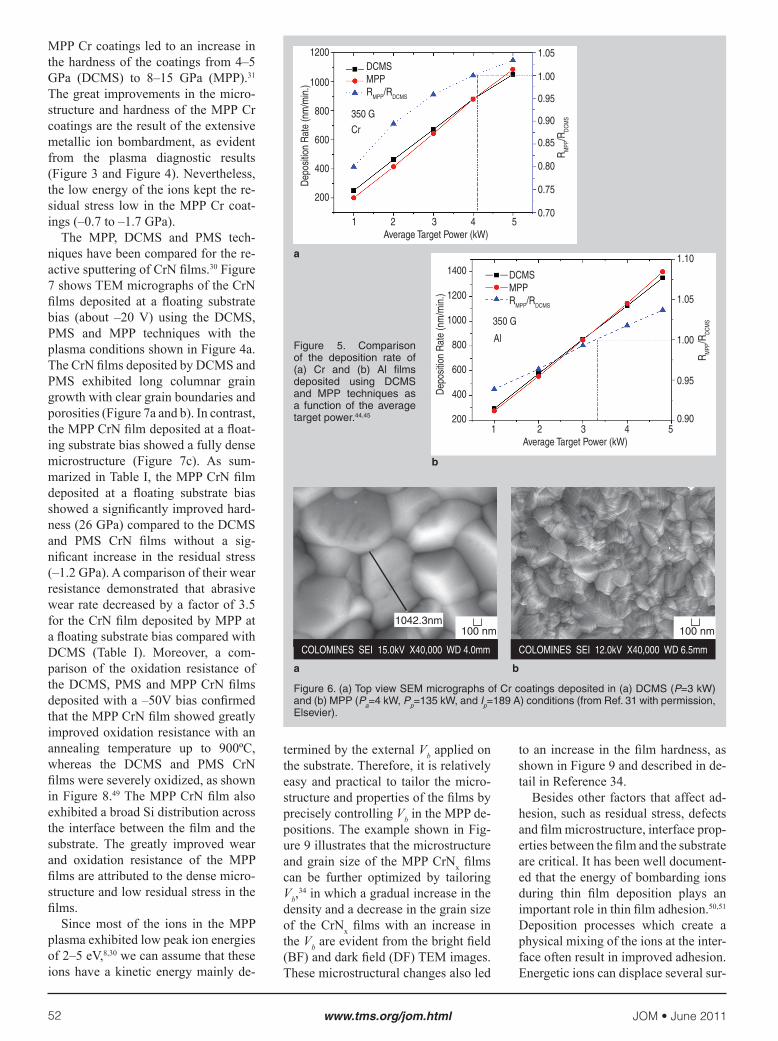
the deposition rate in HPPMS/HIP-IMS is lower than the DCMS rate for an equivalent amount of power.6,11,26,27 However, it has been demonstrated that for some MPP depositions it is possible to deposit films (e.g. Cu, graphite, Al, Ti, and Cr) at rates close to or greater than the rate for DCMS for the same average power.4–7,31 Figure 5 shows the comparison of the deposition rate of Cr and Al materials by the MPP technique as a function of Pa. The parallel com-ponent of the magnetic field strength on the target was 350 G. The ratio of the MPP rate to the DCMS rate gradu-ally increased as Pa was increased for both materials (triangle symbol). The MPP rate exceeds the DCMS rate at Pa=4.2 kW for the Cr material and at a Pa=3.3 kW for the Al material.44,45 Moreover, recent study has shown that the MPP deposition rate can be further increased by decreasing the magnetic field strength and optimizing the puls-ing frequency and pulse length.44 Re-cent research has also shown that the MPP rate is fully comparable with the rate achieved with arc evaporation for the TiAlN coating deposition.46 More-over, the MPP TiAlN coatings exhib-ited longer life, tunable residual stress and improved properties compared to the industrial CAE TiAlN coatings.46 The high deposition rate in the MPP technique is a great advantage and im-provement compared to the traditional HPPMS/HIPIMS technique. This ad-vantage is critical for the commercial production of thin films and coatings with a cost reduction and energy saving.
iMProveMents in the filM Microstructure
and ProPerties
A comparison of the microstructure of the Cr films deposited by DCMS and MPP at similar deposition conditions is shown in Figure 6.31 The DCMS Cr coating deposited at 3 kW exhibited large crystals with the top grain size near 1 mm (Figure 6a). However, the MPP Cr coating deposited at Pa=4 kW, but with a peak pulsed power of 135 kW exhibited much smaller grains with a wide range of grain size distribution (Figure 6b). The laminated feature of the grains indicates that the subgrain growth was significant in the MPP process. The grain refinement in the
Figure 4. Comparison of the IEDs of (a) Cr+ and (b) the integrated Cr+, Ar+ and N+ ion fluxes from the IED curves during reactive sputtering of a CrN film under DCMS, PMS (100 kHz and 60% duty cycle) and two MPP conditions (from Ref. 30 with permission, Elsevier), and (c) the Ipeak and Imean as a function of the Vb during the MPP CrN film depositions.34
a
c
0 10 20 30 40 50Ion Energy (eV)
2.5x10⁶
2.0x10⁶
1.5x10⁶
1.0x10⁶
0.5x10⁶
Inte
nsity
(Cou
nts/
sec)
0 10 20 30 40 50 60 70 80 90 100Ion Energy (eV)
106
105
104
103
102
101
Inte
nsity
(Cou
nts/
sec) 52Cr+
dcMs(1 kW)PMS (1 kW)MPP-1 (1 kW)MPP-2 (4 kW)
b
dcMS PMS MPP-1 MPP-2
7
6
5
4
3
2
1
0
Inte
grat
ed Io
n Fl
ux (x
106 )
52Cr+
40Ar+
28N2+
0 –50 –100 –150Negative Substrate Bias Voltage (V)
300
250
200
150
100
50
0
I Peak
(mA/
cm2 )
100
80
60
40
20
0
I Mea
n (mA/
cm2 )
Peak substrate current densityMean substrate current density
JOM • June 201152 www.tms.org/jom.html
MPP Cr coatings led to an increase in the hardness of the coatings from 4–5 GPa (DCMS) to 8–15 GPa (MPP).31 The great improvements in the micro-structure and hardness of the MPP Cr coatings are the result of the extensive metallic ion bombardment, as evident from the plasma diagnostic results (Figure 3 and Figure 4). Nevertheless, the low energy of the ions kept the re-sidual stress low in the MPP Cr coat-ings (–0.7 to –1.7 GPa). The MPP, DCMS and PMS tech-niques have been compared for the re-active sputtering of CrN fi lms.30 Figure 7 shows TEM micrographs of the CrN fi lms deposited at a fl oating substrate bias (about –20 V) using the DCMS, PMS and MPP techniques with the plasma conditions shown in Figure 4a. The CrN fi lms deposited by DCMS and PMS exhibited long columnar grain growth with clear grain boundaries and porosities (Figure 7a and b). In contrast, the MPP CrN fi lm deposited at a fl oat-ing substrate bias showed a fully dense microstructure (Figure 7c). As sum-marized in Table I, the MPP CrN fi lm deposited at a fl oating substrate bias showed a signifi cantly improved hard-ness (26 GPa) compared to the DCMS and PMS CrN fi lms without a sig-nifi cant increase in the residual stress (–1.2 GPa). A comparison of their wear resistance demonstrated that abrasive wear rate decreased by a factor of 3.5 for the CrN fi lm deposited by MPP at a fl oating substrate bias compared with DCMS (Table I). Moreover, a com-parison of the oxidation resistance of the DCMS, PMS and MPP CrN fi lms deposited with a –50V bias confi rmed that the MPP CrN fi lm showed greatly improved oxidation resistance with an annealing temperature up to 900ºC, whereas the DCMS and PMS CrN fi lms were severely oxidized, as shown in Figure 8.49 The MPP CrN fi lm also exhibited a broad Si distribution across the interface between the fi lm and the substrate. The greatly improved wear and oxidation resistance of the MPP fi lms are attributed to the dense micro-structure and low residual stress in the fi lms. Since most of the ions in the MPP plasma exhibited low peak ion energies of 2–5 eV,8,30 we can assume that these ions have a kinetic energy mainly de-
Figure 5. Comparison of the deposition rate of (a) Cr and (b) Al fi lms deposited using DCMS and MPP techniques as a function of the average target power.44,45
a
b
1 2 3 4 5Average Target Power (kW)
1200
1000
800
600
400
200
Dep
ositi
on R
ate
(nm
/min
.)
1.05
1.00
0.95
0.90
0.85
0.80
0.75
0.70
RM
PP/R
DC
MS
Cr
350 G
DCMSMPPRMPP/RDCMS
1 2 3 4 5Average Target Power (kW)
Dep
ositi
on R
ate
(nm
/min
.)
1400
1200
1000
800
600
400
200
RM
PP/R
DC
MS
1.10
1.05
1.00
0.95
0.90
DCMSMPPRMPP/RDCMS
350 G
Al
Figure 6. (a) Top view SEM micrographs of Cr coatings deposited in (a) DCMS (P=3 kW) and (b) MPP (Pa=4 kW, Pp=135 kW, and Ip=189 A) conditions (from Ref. 31 with permission, Elsevier).
a b
COLOMINES SEI 15.0kV X40,000 WD 4.0mm
100 nm1042.3nm
100 nm
COLOMINES SEI 12.0kV X40,000 WD 6.5mm
termined by the external Vb applied on the substrate. Therefore, it is relatively easy and practical to tailor the micro-structure and properties of the fi lms by precisely controlling Vb in the MPP de-positions. The example shown in Fig-ure 9 illustrates that the microstructure and grain size of the MPP CrNx fi lms can be further optimized by tailoring Vb,
34 in w hich a gradual increase in the density and a decrease in the grain size of the CrNx fi lms with an increase in the Vb are evident from the bright fi eld (BF) and dark fi eld (DF) TEM images. These microstructural changes also led
to an increase in the fi lm hardness, as shown in Figure 9 and described in de-tail in Reference 34. Besides o ther factors that affect ad-hesion, such as residual stress, defects and fi lm microstructure, interface prop-erties between the fi lm and the substrate are critical. It has been well document-ed that the energy of bombarding ions during thin fi lm deposition plays an important role in thin fi lm adhesion.50,51 Deposition processes which create a physical mixing of the ions at the inter-face often result in improved adhesion. Energetic ions can displace several sur-

Vol. 63 No. 6 • JOM 53www.tms.org/jom.html
Figure 7. Cross-sectional TEM images of CrN coatings deposited under (a) DCMS, (b) PMS (100 kHz and 60% duty cycle) and (c) MPP (Pp=180 kW and Ip=250 A) conditions at a fl oating substrate bias (H=nanoindentation hardness, σ=residual stress (from Ref. 30 with permis-sion, Elsevier).
a b c
DCMSH = 16 GPaσ = –0.9 GPa
100 nm
voids
PMSH = 21 GPaσ = –2 GPa
100 nm
voids
(311)(200)
(111)(220)
100 nm
MPPH = 26 GPaσ = –1.2 GPa
(311)(200)
(111)(220)
Figure 8. Cross-sectional SEM micrographs of the CrN coatings deposited by (a) DCMS, (b) PMS and (c) MPP techniques after annealling in an ambient air at 900ºC for one hour.49
a b c1 mm 1 mm 1 mm
Cr Si O N Cr Si O N Cr Si O N
Figure 9 BF and DF TEM images of the CrNx fi lms deposited by MPP at different negative substrate bias voltages: (a) 0 V, (b) –50 V, and (c) –150 V.34 ( H=nanoindentation hardness).
a b c
0V
H = 22 GPa
(111)(200)
(220)
100 nm
–50 V
H = 26 GPa
(111)(200)
(220)
20 nm
–150 V
H = 28 GPa
(002)(111)
(300)(302)
10–15 nm
50 nm
Figure 10. (a) Cross-sec-tional TEM micrograph showing the lattice mixing at the interface between the MPP CrN fi lm and Si substrate;53 and (b) the scratch track morpholo-gies of CrN coatings de-posited by DCMS, PMS and MPP (Pp=180 kW and Ip=250 A) on soft AISI 304 stainless steel and hard tool steel substrates (from Ref. 30 with permis-sion, Elsevier).
a b
DCMS CrN on soft stainless steel
PMS CrN on soft stainless steel
MPP CrN on soft stainless steel
MPP CrN on hard tool steel10 nm
Interface
d = 3.1 ÅSi (111)
d = 1.9 ÅCrN (200)

JOM • June 201154 www.tms.org/jom.html
face and sub-surface atoms in a cascad-ing effect (ion mixing), resulting in the sputtering of surface contaminants and increased film/substrate-interface dif-fusion.52 One of the potential benefits of HPPMS is the enhancement of ad-hesion of the films.3 Ehiasarian et al.24 used sputtering pretreatment with HIP-IMS for CrN film deposition and found better adhesion when compared to a normal magnetron sputter etching pro-cess with argon, and the critical load for a scratch test increased from 40 N to 90 N. The examination of the inter-face between a MPP CrN film and the Si substrate in TEM (Figure 10a) has shown that the interface is extremely dense and continuous.53 The intermix-ing of the lattice fringes between the Si (111) and the CrN (200) planes can be observed from the TEM image. The increased lattice plane mixing at the interface from the high metallic ion flux generated from MPP plasma was attributed to great improvements in the film adhesion. Micro-scratch tests per-formed on the DCMS, PMS and MPP CrN films deposited on soft stainless steel and hard tool steel substrates have demonstrated that the films deposited by MPP exhibited superior adhesion strength (Figure 10b).30 The excellent adhesion of the MPP coatings has also been observed for the thick coatings
Table I. Comparison of the Properties of the CrN Thin Films and Thick Coatings Deposited by Different Magnetron Sputtering Techniques*
CrN N/Crt
(mm)Stress(GPa)
H(GPa)
E(GPa) H/E COF
Wear Rate(×10–7
mm3N–1m–1)Lc(N) Ref.
DCMS (floating)
0.98 2.5 –0.9 16 280 0.057 0.58 87.5 >30 30
PMS (floating)
0.94 2.0 –2.0 21 256 0.082 0.45 36.5 23 30
MPP (floating)
0.96 2.7 –1.2 26 310 0.084 0.33 24 >30 30
MPP (–50V)
0.98 3.5 -–2.5 26 320 0.081 0.46 6-10 N/A 47
Multi Pulse MPP (–50V)
0.95 3.2 –2.7 30.5 336 0.091 0.42 2.1 N/A 47
10 mm MPP (–50 V)
1.07 10 –4.0 24.9 290 0.086 0.48 2.2 >30 48
55 mm MPP (–50V)
1.05 55 –4.0 22.1 275 0.080 0.57 3.9 >90 48
* t=thickness, Lc=scratch test critical load on AISI 304 substrate)
(e.g. 55 mm CrN and 100 mm Ta coat-ings) in the progressive scratch test, which will be illustrated later.
structurally laMinated
nanostructure in Multi-Pulse MPP filMs
There is another important feature of the MPP technique. Besides its capabil-ity to use one single pulse shape on the target, it can rapidly switch between different pulse shapes and maintain each pulse shape for specific durations. Figure 11a illustrates the concept of the multi-pulse MPP (MPMPP) technique, in which two pulse shapes (I and II) with different pulse widths of 750 and 1000 ms were alternately switched on for durations of times, t1 and t2, re-spectively. The interval between two pulses is 150 ms. Different pulsing parameters in each pulse shape lead to different Pp, Vp, and Ip generated on the target which will change the plas-ma properties in each pulse duration, and thereby depositing a structurally laminated film from the same target material.47 Figure 11b shows the cross-sectional TEM image of a CrN film deposited by the MPMPP technique. It is evident that a structurally laminated nanolayer architecture was formed. The layer thickness is about 8 nm in
this film. The hardness of this film was 30.5 GPa, which was greater than the hardness of the CrN film deposited by the single pulse MPP (26 GPa) and was much higher than that of the DCMS and PMS CrN films (16 GPa and 21 GPa, respectively). In addition, the residual stress in this MPMPP coating is relatively low (–2.7 GPa) (Table I). The MPMPP film also exhibited great-ly improved wear resistance, e.g. a low COF of 0.42 and the wear rate in the low 10–7 mm3N–1m–1 range. A compari-son of the mechanical and tribological properties of the DCMS, PMS, single pulse, and multi-pulse MPP CrN films has been summarized in Table I. This new feature of the MPMPP technique opens great opportunities to further op-timize the structure and properties of the films by combining the low energy and high ion flux bombardment with the structural modulation.
dense, low stress, well adherent thick coating dePosition
It is highly desirable to increase the life and performance of the hard protective coating by applying a rela-tively thick coating (e.g. > 6 mm). Many other thick coating preparation techniques (e.g. electroplating,54 ther-mal plasma spraying,55 CAE,56 and chemical vapor deposition (CVD),57 etc.) have good process stability and in many cases low costs, and they have been adapted for industrial produc-tion. Nevertheless, some of the above techniques such as electroplating are not environmental friendly, and the coatings can exhibit low density, poor adhesion, and poor properties that re-strict their use for a number of applica-tions. Magnetron sputtering technique can overcome many of the above listed disadvantages. However, compared to other PVD processes such as CAE, the sputter deposition rate usually is not as high as that for CAE. In addition, the thickness of sputter deposited coat-ings is often limited by the adhesion strength, the thermal stresses generated by differences in the coefficient of ther-mal expansion between the coating and the substrate material, combined with the intrinsic stress that builds up in the coating during the deposition, which is directly affected by the ion energy and

Vol. 63 No. 6 • JOM 55www.tms.org/jom.html
energy/high ion fl ux bombardment to achieve dense coatings with low stress and defect incorporations. Recently, Lin et al. has reported the successful depositions of 10–55 mm thick CrN and Cr2N coatings, and 100 mm a-Ta conformal coatings using MPP at high deposition rates (e.g. 10 mm/hr for the CrN, 15 mm/hr for the Cr2N and 16 mm/hr for a-Ta).32,48 These thick coatings showed extremely dense microstructures and fi ne grain sizes (Figure 12). The residual stresses of these thick coatings are relatively low, in the range of –2 GPa to –5.5 GPa, as labeled in Figure 12. On account of their dense microstructures, the thick MPP coatings also exhibited excellent adhesion and mechanical and tribologi-
cal properties. The mechanical proper-ties of the thick MPP CrN coatings (Table I) are comparable to those de-posited by traditional CAE and magne-tron sputtering techniques. Progressive scratch tests performed on a 55 mm CrN and a 100 mm a-Ta coatings showed no coating failure at a maximum load of 100 N (Figure 13a and b) on different substrates. The excellent adhesion of the thick MPP coatings is attributed to the low residual stress in the coatings and the strong bonding force between the coating and the substrate, which benefi ted from the enhanced ion bom-bardment from the highly ionized MPP plasma. The thick MPP CrN coating (>10 m m) exhibited signifi cantly im-proved wear resistance compared to
ion fl ux arriving at the substrate. The traditional PMS and HPPMS/HIPIMS depositions exhibit a low de-position rate and contain a wide range of ion energy distributions (up to 100 eV).9,41 The high energetic ion bom-bardment (>80 eV) can also induce residual stress and point/line defects in the growing fi lm,40 which are detrimen-tal to thick coating growth. In contrast, the MPP technique can achieve a high deposition rate (Figure 5) while at the same time achieve a high degree of ionization of the sputtered mate-rial with low ion energies (2–5 eV) (Figures 3 and 4). Thus it is practi-cal to deposit thick coatings using the MPP technique by taking advantage of its high deposition rate and ideal low
Figure 11. (a) Schematic drawing shows multi pulse MPP magnetron sputtering for deposit-ing structurally laminated thin fi lms from the same target material; (b) cross-sectional TEM image of a MPMPP CrN fi lm showing the modulation period of 8 nm within the columnar grains.47
a
b
Figure 12 Cross-sectional SEM images of thick CrN and Ta coatings deposited by the MPP technique with high deposition rates: (a) a 55 mm CrN coating (10 mm/h) (from Ref. 48 with permission, Elsevier), (b) a 55 mm Cr2N coating (15 mm/h) (from Ref. 48 with permission, Elsevier), and (c) a 100 mm a-Ta coating (16 mm/h) (from Ref. 32 with permission, IEEE).
a b c
H = 24 GPaσ = –2 GPa σ = –2.1 GPa
a 55 mm Cr2N coating a 100 mm Ta coating
Ta coating 100 mm
COLOMINES SEI 10.0kV X1,500 WD 4.0mm
10 mm 10 mm10 mm
COLOMINES SEI 10.0kV X1,500 WD 4.0mm COLOMINES SEI 5.0kV X700 WD 6.6mm
Structural modulation
2000
-200-400-600
0 200 400 600 800 1000Time (ms)
2000
-200-400-600
2000
-200-400-600
2000
-200-400-600
0 200 400 600 800 1000Time (ms)
0 200 400 600 800 1000 1200Time (ms)
0 200 400 600 800 1000 1200Time (ms)
Current Current
Power PowerVoltage Voltage
Current Current
Power PowerVoltage Voltage
750 ms 750 ms 1000 ms 1000 ms Time
Volta
ge, C
urre
nt, P
ower
Duration t2 (e.g. 5s)Rep. rate 42 Hz
Duration t1 (e.g. 5s)Rep. rate 180 Hz
150ms
Pulse Shape IIPulse Shape I
Ip = 97 A, Pp = 46 kW Ip = 211 A, Pp = 113 kW
750 ms 750 ms 1000 ms 1000 ms Time
MPMPPH = 30.5 GPaσ = –2.7 GPa
(111)
(200)(220)
20 nm
8 nm
H = 22 GPaσ = –4 GPa
a 55 mm CrN coating

JOM • June 201156 www.tms.org/jom.html
a
b
Figure 13 Friction force versus applied load during the progressive load scratch tests per-formed on (a) a 55 mm CrN (from Ref. 48 with permission, Elsevier) and (b) a 100 mm a-Ta coatings. (The insert SEM images show the end of the scratch track of the coatings;) (from Ref. 32 with permission, IEEE). (c) COF and wear rate of the MPP sputtered CrN coatings with different coating thicknesses (from Ref. 48 with permission, Elsevier).
c
10 20 30 40 50 60 70 80 90 100Normal Load (N)
60
50
40
30
20
10
0
Fric
tion
Forc
e (N
)
No Coating Failure
––55 mm CrN Coating WC - Co Substrate
COLOMINES SEI 5.0kV X850 WD 4.1mm
10 mm
10 20 30 40 50 60 70 80 90 100Normal Load (N)
200
150
100
50
Fric
tion
Forc
e (N
)
No Coating Failure
––100 mm Ta Coating AISI 304 Substrate
100 mm
COLOMINES SEI 10.0kV X100 WD 4.1mm
0 10 20 30 40 50 60 Coating Thickness (mm)
0.7
0.6
0.5
0.4
0.3
0.2
0.1
Coe
ffici
ent o
f Fric
tion
2.4x10⁻⁶
2.0x10⁻⁶
1.6x10⁻⁶
1.2x10⁻⁶
8.0x10⁻⁷
4.0x10⁻⁷
Wea
r Rat
e (m
m3 N
–1m
–1)
Coefficient of Friction
Wear Rate
0.38 to 0.56 as the coating thickness was increased. However, the coatings showed pronounced improvements in the wear resistance as the coating thickness increased above 5 mm. The 2.5 mm thin CrN film exhibited a wear rate of 1.1×10⁻⁶ mm3N–1m–1. The wear
rate of the CrN coating decreased by a factor of 5 as the coating thickness was increased to 10 mm (2.2×10⁻⁷ mm3N–
1m–1) and remained in the low 4~5 ×10⁻⁷ mm3N–1m–1 range as the coating thickness was further increased. The significant decrease in the wear rate of the thick CrN coatings (>10 mm) as compared to the thin CrN films can be attributed to the improved load carry-ing capacity and the increased scratch critical load as the coating thickness was increased.48 Since the coating is much harder than the steel substrate, the applied normal load during the wear test becomes more substantially supported by the harder coating as the coating thickness is increased.
conforMal coating dePosition using MPP
Conformal coating deposition is im-portant for precision cutting and form-ing tools, semiconductor chip and mi-croelectronic devices, magnetic discs, and biomedical implant fabrication. Nevertheless, it is a challenge to coat complex-shaped substrate/components in most PVD processes (e.g. magne-tron sputtering) due to the line-of-sight limitation. However, as the deposited species are largely metallic ions in the MPP/HPPMS plasma, it is possible to control the metal ion trajectory by bi-asing the substrate to improve the step coverage and achieve good deposition rate on the surface placed at an angle to the target. Early work by Alami et al.21 showed that the Ta thin films grown on a Si substrate placed along the wall of a trench by HPPMS exhibited a denser microstructure and a higher deposition rate than the film grown by dc magne-tron sputtering at the same location. Recently, Lin et al.32 have deposited an 80 µm a-Ta coating on the steel sub-strate placed with one side facing the target surface and the other side orthog-onal to the target using the MPP tech-nique with a –50 V dc substrate bias. As shown in Figure 14, the thickness of the coating on the orthogonal side is 65 mm, which is 81% of the thickness of the coating deposited on the side facing the target (80 µm). Considering the large thickness of the coating, the good homogeneity achieved by MPP is a direct consequence of the high ion fraction of sputtered species being con-
the thin films (e.g. 2.5 mm). Figure 13c shows the COF and wear rate of the MPP thick CrN coatings sliding against a 5 mm Al2O3 ball at a 10 N load with a 200 rpm rotation speed for a travel length of 2,000 meters. The COF of the coatings gradually increased from

Vol. 63 No. 6 • JOM 57www.tms.org/jom.html
trolled by the bias on the substrate.
suPerlattice coatings dePosited using the coMBined MPP+PMs
techniQue
The development of nanostructured superlattice coatings over the past de-cade has shown considerable improve-ments in comparison to traditional monolithic hard coatings in terms of their increased hardness and superior wear resistance,58,59 e.g. TiN/VN,60 TiN/NbN,61 TiN/CrN,62 CrN/AlN.63,64 The superlattice coatings have shown great potential in machining, metal form-ing and wear resistance applications. However, the major obstacles for the industrial production of the superlattice coatings includes the requirements of the complex substrate rotation system, low deposition rate and limited coat-ing thickness due to the signifi cantly increased internal stress as the thick-ness of the coating increased caused by the lattice and composition mismatches between the heterogeneous nanolayers. Recent advances in the MPP tech-
nique include the deposition of high performance thick superlattice coat-ings with a high deposition rate using the combined MPP+PMS tech nique. Figure 15 shows an example confi gura-tion of the deposition of a CrN/AlN su-perlattice coating using the combined MPP+PMS technique. The Al target was powered by a PMS power source (Advanced Energy Pinnacle Plu s), and the Cr target was powered by an MPP power source (Zpulser, LLC.). It can be seen that an extremely dense plasma has been achieved by the combined MPP+PMS technique. By manipulat-ing the power, the pulsing conditions and the substrate rotation speed, CrN/AlN coatings with a range of modula-tion periods from 2 to 15 nm have been prepared by the combined MPP+PMS technique with high deposition rates of 30–110 nm/min.65 Figure 15b and c shows the cross-sectional SEM mi-crographs of a 7 mm CrN/AlN super-lattice coating with a bilayer period of 10.1 nm deposited using this combined technique. The coating exhibited an extremely dense microstructure, fi ne
grains and smooth surface (Figure 15b). A slight cha nge in the fracture morphology near the surface region was observed, which is probably be-cause of a change in the residual stress along the thick coating. Superhardness values of 40–45 GPa and low wear rates in the 10–8 mm3N–1m–1 range have been readily achieved in these CrN/AlN coatings with an optimized bilayer period in the range of 2.5 to 3.5 nm. It is expected that high quality superlat-tice coatings with the thickness of more than 10 mm can be feasibly deposited by the combined MPP+PMS technique with a high deposition rate.
conclusion
There is a great need to develop high performance fi lms and coatings that exhibit superior performance under harsh environments (high temperature, oxidation and corrosion), coupled with high hardness, good wear resistance, increased toughness and increased coating thickness. This range of multi-functional properties can be achieved by depositing the fi lms from a highly ionized metal plasma vapor deposi-tion with the modulated pulsed power (MPP) magnetron sputtering tech-nique. The MPP technique is still in its early development stage. However, the research work reviewed in this article has demonstrated that the MPP tech-nique provides a controlled low ion energy and high metallic ion fl ux, that densifi es the growing fi lm, improves the adhesion, and controls the micro-structure. It also has been demonstrated that MPP sputtering has the potential for providing thicker coatings and in-creased conformal coverage at a high deposition rate without detrimental in-creases in stress and defects.
acknowledgeMent
Part of the research work supported by the US Army and the North Ameri-can Die Casting Association (NADCA) is gratefully acknowledged. We are grateful for the valuable discussions from Dr. John A. Rees, Dr. David N. Ruzic, and Dr. Malki Pinkas. We are also grateful for the help from Dr. Mi-chael J. Kaufman, Mr. Gary Zito, and Dr. John P. Chandler at the Elect ronMicroscopy Laboratory of the Depart-ment of Metallurgical and Materials
Figure 14. Optical im-ages of an 80 mm thick a-Ta coating deposited using MPP showing a good homogeneity of the coating coverage on the side orthogonal to the target (from Ref. 32 with permission, IEEE).
The thickness of a thick Ta coating on the side orthogonal to the target is of about 81% of the thickness on the side facing the target.
Facing the target
Orthogonal to the target
65 mm
80 mm
50 mm
200 mm50 mm
Figure 15. (a) A photo shows the confi guration of the combined MPP+PMS deposition; (b) c ross-sectional SEM micrograph of a 7 mm CrN/AlN superlattice coating deposited by the combined MPP+PMS technique; (c) cross-sectional SEM micrograph showing the bilayer period of 10.1 nm of the coating.65
b c
Al-PMS Substrate Cr-MPP
141.6nm
7 mm
1 mm100 nm
SEI 5.0kV X10,000 WD 4.0mma X100,000 WD 4.0mm

JOM • June 201158 www.tms.org/jom.html
Engineering at the Colorado School of Mines.references
1. V. Kouznetsov, K. Macák, J.M. Schneider, U. Hel-mersson, and I. Petrov, Surf. Coat. Technol., 122 (1999), pp. 290–293.2. K. Macák, V. Kouznetsov, J. Schneider, U. Helmers-son, and I. Petrov, J. Vac. Sci. Technol. A, 18(4) (2000), pp. 1533–1537.3. U. Helmersson, M. Lattemann, J. Bohlmark, A.P. Ehiasarian, and J.T. Gudmundsson, Thin Solid Films, 513 (2006), pp. 1–24.4. R. Chistyakov, B. Abraham, and W.D. Sproul, Pro-ceedings of the 49th Annual SVC Technical Conference (Washington, DC, April 23–27, 2006), pp. 88–91.5. R. Chistyakov, B. Abraham, W. Sproul, J. Moore, and J. Lin, Proceedings of the 50th Annual SVC Technical Conference (Louisville, KY, April 30–May 3, 2007), pp. 139–143.6. W.D. Sproul, D.J. Christie, and D.C. Carter, Proceed-ings of the 47th Annual SVC Technical Conference (Dallas, Texas, April 25–29, 2004), pp. 96–100.7. W.D. Sproul, R. Chistyakov, and B. Abraham, Society of Vacuum Coaters News Bulletin (Summer 2006), pp. 35–37.8. J. Lin, J.J. Moore, W.D. Sproul, B. Mishra, J.A. Rees, Z. Wu, R. Chistyakov, and B. Abraham, Surf. Coat. Technol., 203 (2009), pp. 3676–3685.9. J. Bohlmark, M. Lattemann, J.T. Gudmundsson, A.P. Ehiasarian, Y. Aranda Gonzalvo, N. Brenning, and U. Helmersson, Thin Solid Films, 515 (2006), pp. 1522–1526.10. D.J. Christie, F. Tomasel, W.D. Sproul, and D.C. Carter, J. Vac. Sci. Technol. A, 22 (4) (2004), pp. 1415–1419.11. U. Helmersson, M. Lattemann, J. Bohlmark, A.P. Ehiasarian, and J.T. Gudmundsson, Thin Solid Films, 513 (2006), pp. 1–24.12. J. Vlček, P. Kudláček, K. Burcalová, and J. Musil, J. Vac. Sci. Technol. A, 25 (1) (2007), pp. 42–47.13. P. Poolcharuansin and J.W. Bradley, Plasma Sourc-es Sci. Technol., 19 (2010), p. 025010.14. D. Lundin, P. Larsson, E. Wallin, M. Lattemann, N. Brenning, and U. Helmersson, Plasma Sources Sci. Technol., 17 (2008), p. 035021.15. A.P. Ehiasarian, P.Eh. Horsepian, L. Hultman, and U. Helmersson, Thin Solid Films, 457 (2004), pp. 270–277.16. J. Alami, K. Sarakinos, F. Uslu, and M. Wuttig, J. Phys. D: Appl. Phys., 42 (2009), p. 015304.17. K. Sarakinos, J. Wördenweber, F. Uslu, P. Schulz, J. Alami, and M. Wuttig, Surf. Coat. Technol., 202 (2008), pp. 2323–2327.18. S. Konstantinidis, J.P. Dauchot, and M. Hecq, Thin Solid Films, 515 (2006), pp. 1182–1186.19. V. Sittinger, F. Ruske, W. Werner, C. Jacobs, B. Szyszka, and D.J. Christie, Thin Solid Films, 516 (2008), pp. 5847–5859.20. C. Reinhard, A.P. Ehiasarian, and P.Eh. Hovsepian, Thin Solid Films, 515 (2007), pp. 3685–3692.21. J. Alami, P.O.Å. Persson, D. Music, J.T. Gudmunds-son, J. Bohlmark, and U. Helmersson, J. Vac. Sci. Tech-nol., A23 (2) (2005), pp. 278–280.22. K. Bobzin, N. Bagcivan, P. Immich, S. Bolz, R. Cre-mer, and T. Leyendecker, Thin Solid Films, 517 (2008), pp. 1251–1256.23. M. Lattemann, A.P. Ehiasarian, J. Bohlmark, P.O.
Persson, and U. Helmersson, Surf. Coat. Technol., 200 (2006), p. 6495.24. A.P. Ehiasarian, J.G. Wen, and I. Petrov, J. Appl. Phys., 101 (2007), p. 054301.25. K. Sarakinos, J. Alami, and M. Wuttig, J. Phys, D: Appl. Phys., 40 (2007), pp. 2108–2114.26. K. Sarakinos, J. Alami, and S. Konstantinidis, Surf. Coat. Technol., 204 (2010), pp. 1661–1684.27. A. Anders, J. Vac. Sci. Technol. A, 28 (4) (2010), pp. 783–790.28. D.J. Christie, J. Vac. Sci. Technol. A, 23 (2) (2005), pp. 330–335.29. D.J. Christie, Czechoslovak Journal of Physics, 56 (2006), Suppl. B, pp. B93–B97.30. J. Lin, J.J. Moore, W.D. Sproul, B. Mishra, Z. Wu, and J. Wang, Surf. Coat. Technol., 204 (2010), pp. 2230–2239.31. J. Lin, J.J. Moore, W.D. Sproul, B. Mishra, and Z. Wu, Thin Solid Films, 518 (2009), pp. 1566–1570.32. J. Lin, John J. Moore, W.D. Sproul, Sabrina L Lee, and Jun Wang, IEEE Transactions on Plasma Science: Special Issue on HIPIMS and High Power Glow Dis-charges, 38 (11) (2010), pp. 3071–3078.33. W.D. Sproul, J. Lin, J.J. Moore, S.L. Lee, and J. Wang, Proc. 53rd Annual Technical SVC Technical Conference (Orlando, FL, April 17–22, 2010), pp. 187–192.34. J. Lin, W.D. Sproul, J.J. Moore, and S.L. Lee, “Effect of Negative Substrate Bias Voltage on the Structure and Properties of CrN Films Deposited by Modulated Pulsed Power (MPP) Magnetron Sputtering,” J. Phys. D:Appl. Phys., (2011) submitted for publication.35. W.D. Sproul, P.J. Rudnik, M.E. Graham, and S.L. Rohde, Surf. Coat. Technol., 43-44 (1990), pp. 270–278.36. S.L. Rohde, I. Petrov, W.D. Sproul, S.A. Barnett, P.J. Rudnik, and M. E. Graham, Thin Solid Films, 193 (1990), pp. 117–126.37. L. Meng, A.N. Cloud, S. Jung, and D.N. Ruzic, J. Vac. Sci. Technol. A, 29 (1) (2011), p. 011024-1.38. B. Liebig, N.St.J. Braithwaite, P.J. Kelly, R. Chistya-kov, B. Abraham, and J.W. Bradley, Surf. Coat. Technol. (2011) doi: 10.1016/j.surfcoat.2011.01.017.39. I. Petrov, L. Hultman, U. Helmersson, J.-E. Sund-gren, and J.E. Greene, Thin Solid Films, 169 (1989), pp. 299–314.40. I. Petrov, P. B. Barna, L. Hultman, and J. E. Greene, J. Vac. Sci. Technol. A, 21 (2003), p. S117.41. J. Lin, J.J. Moore, B. Mishra, M. Pinkus, W.D. Sproul, and J.A. Rees, Surf. Coat. Technol., 202 (2008), pp. 1418–1436.42. W.D. Sproul, Surf. Coat. Technol., 81 (1996), pp. 1–7.43. J.E. Greene, J-E. Sundgren, L. Hultman, I. Petrov, and D.B. Dergstrom, Appl. Phys. Lett., 67 (20) (1995), pp. 2928–2930.44. J. Lin, W.D. Sproul, and J.J. Moore, “Infl uence of the Magnetic Field Strength on the Deposition Rate of Modulated Pulsed Power (MPP) Magnetron Sputtering of Metallic Thin Films” (Paper presented at the AVS 57th International Symposium & Exhibition, October 17–22, 2010, Albuquerque, New Mexico).45. J. Lin, W.D. Sproul, and J.J. Moore, “Effects of the Magnetic Field Strength on the DC Magnetron Sput-tering and Modulated Pulsed Power Magnetron Sput-tering of Metallic Films,” J. Vac. Sci. Tech. A (2011), submitted for publication. 46. F. Papa and L. Peeters, “Excellent Test Results HIPIMS+,” Hauzer for You, 16 (Hauzer Techno Coating
BV, The Netherlands; [email protected]) (2010), pp. 3–7.47. J. Lin, W.D. Sproul, and J.J. Moore, “Structurally Laminated CrN Films Deposited by Multi Pulse Modu-lated Pulsed Power (MPMPP) Magnetron Sputtering,” Surf. Coat. Technol., submitted for publication.48. J. Lin, W.D. Sproul, J.J. Moore, S.L. Lee, and S. My-ers, Surf. Coat. Technol., 205 (2011), pp. 3226–3234.49. J. Lin, W.D. Sproul, and J.J. Moore, “A Comparison of the Oxidation Behavior of CrN Films Deposited us-ing Continuous dc, Pulsed dc and Modulated Pulsed Power (MPP) Magnetron Sputtering” Surf. Coat. Tech-nol. (2011) submitted for publication. 50. J.A. Thornton, Annual Review of Materials Sci-ence, 7 (1997), pp. 239–260.51. D.L. Smith, Thin Film Deposition (New York: Mc- Graw-Hill, 1995), pp. 197–200.52. J. Baglin, Handbook of Ion Beam Processing Tech-nology: Principle, Deposition, Film Modifi cation and Synthesis (Westwood, NJ: Noyes Publications, 1989), pp. 279–299.53. J. Lin, W.D. Sproul, and J.J. Moore, unpublished work (2011).54. N. Kanani, Electroplating- Basic Principles (Oxford, U.K.: Processes and Practice, 2005).55. L. Pawlowski, The Science and Engineering of Thermal Spray Coatings (New York: John Wiley, 1995).56. D.A. Karpov, I.F. Kislov, A.I. Ryabchikov, and A.A. Ganenko, Surf. Coat. Technol., 89 (1997), pp. 58–61.57. D.W. Wheeler and R.J.K. Wood, Wear, 225-229 (1999), pp. 523–536.58. W. D. Sproul, Science, 273 (1996), pp. 889–892.59. P.C. Yashar and W.D. Sproul, Vacuum, 55 (1999), pp. 179–190.60. U. Helmersson, S. Todorova, S. A. Barnett, J.-E. Sundgren, L.Co. Markert, and J.E. Greene, J. Appl. Phys., 62 (2) (1987), pp. 481–484.61. X. Chu, S.A. Barnett, M.S. Wong, and W.D. Sproul, Surf. Coat. Technol., 57 (1993), pp. 13–18.62. M. Nordin and M. Larsson, Surf. Coat. Technol., 116-119 (1999), pp. 108–115.63. J. Lin, J.J. Moore, B. Mishra, M. Pinkas, and W.D. Sproul, Surf. Coat. Technol., 204 (2009), pp. 936–940.64. J. Lin, B. Mishra, J.J. Moore, X.H. Zhang, and W.D. Sproul, Thin Solid Films, 517 (2009), pp. 5798–5804.65. J. Lin, W.D. Sproul, and J.J. Moore, “Thick CrN/AlN Superlattice Coatings Deposited by the Combined Pulsed DC Magnetron Sputtering (PMS) and Modulat-ed Pulsed Power (MPP) Magnetron Sputtering Tech-nique,” unpublished work (2011).
Jianliang Lin, research assistant professor, Wil-liam D. Sproul, research professor, John J. Moore, Trustee’s professor, and Zhili Wu, lecturer, are with the Advanced Coatings and Surface Engineering Laboratory (ACSEL), Department of Metallurgical and Materials Engineering, Colorado School of Mines, Golden, Colorado, 80401; Sproul is also founder and owner of Reactive Sputtering, Inc., San Marcos, California, 92078; Wu is also with the Surface Engineering Laboratory, School of Materi-als Science and Engineering, Dalian University of Technology, Dalian 116024, China; Sabrina Lee, physicist, is with U.S. Army Benet Laboratories, Watervliet Arsenal, NY 12189; Roman Chistyakov, president, Zond, Inc., Mansfi eld, MA; and Bassam Abraham, president, Zpulser, LLC, Mansfi eld, Mas-sachusetts, 02048. Dr. Lin can be reached at [email protected].
John J. Moore is a TMS Member!
To read more about him, turn to page 10. To join TMS, visit www.tms.org/Society/Membership.aspx.