
Power MOSFET Failures in Automotive Applications - Vishay · Power MOSFETs Application Note 910...
8
Document Number: 69294 www.vishay.com Revision: 27-Apr-09 1 VISHAY SILICONIX Power MOSFETs Application Note 910 Power MOSFET Failures in Automotive Applications APPLICATION NOTE By Kandarp Pandya, Klaus Pietrczak, Arthur Chiang, Greg Getzan There is no more demanding environment for power MOSFETs than automotive systems. As the components controlling the power for on-board electronics, MOSFETs in automotive systems are frequently used close to their electrical and thermal absolute maximum ratings in an effort to maximize power-to-weight ratios, i.e. to minimize material usage and minimize the physical volume of circuitry, in addition to cutting costs. Design engineers have at their disposal sophisticated analysis tools to verify the adequacy of each component. Failure rates are extremely low, on the order of a few per million. The rarity of failure makes it extremely difficult to identify the cause of those failures that do occur. Collaborative efforts from both power MOSFET manufacturers and automotive design and manufacturing houses are required to reach successful solutions, and in many cases, proving the effectiveness of these solutions is extremely difficult due to the low failure rates involved. Battery connect/disconnect switches implemented with power MOSFETs as a high-side switch (figure 1) are an example of circuits that experience a failure rate of a few parts per million. In this application, the drain of the MOSFET is permanently connected to the vehicle battery; the floating gate drive comes from a custom ASIC chip. The output voltage of the ASIC tracks the source potential and maintains the required gate drive voltage. However, the ASIC often has limited current sourcing capabilities. The source feeds into the other circuit controls; it also powers MOSFETs connected in parallel. In many cases, this load is inductive, with or without recirculation of its stored energy. An understanding of the susceptibility of the MOSFET in this application requires studying the prime suspects, such as load dumping from a bad connection on the battery, the gate drive capabilities of the ASIC, and inductive surges from parallel connected loads on the source (the lower leg). Invariably, the results from circuit analysis are negative, with no clear root cause of device failure. This is not surprising since failures are so rare and measured in the low parts-per-million. Failure analysis performed at MOSFET manufacturing facilities can provide further insights into the actual device failure mechanisms. Basic electrical tests can indicate gate-to-source, gate-to-drain, and drain-to-source leakages with low resistance values. Examples of systematic decapsulation of failed devices are shown in figures 2 to 7. It can be observed that failures occur in two areas of the MOSFET structure. One failure is from gate metal to drain poly and the other failure is from source metal to gate poly. The conclusion from the analysis is that some voltage transient occurs on the gate and leads to the failure. Excluding the cases of obvious processing anomalies, investigations into the manufacturing processes have shown that these items are unlikely to be the cause of failure. The reasoning behind this conclusion takes into account the very low failure rates seen and fact that individual failures tend to occur across multiple wafer and assembly lots. Process investigation into the history of failed devices invariably shows that all critical parameters were well within the normal distribution, and corresponding final production test data were free from any objectionable deviations. At this point, every device is like every other device in all measurable ways. For the root cause analysis, the key question is what kind of electrical transient could lead to such a failure? The failure is clearly caused after the device has completed the manufacturer's production testing, which significantly limits the possible causes of inducing failure. Device failure after this operation could be a result of handling or an actual application issue. ESD testing to evaluate handling problems, followed by failure analysis, has not produced identical failure signatures. Similarly, application analysis and assembly level testing has yielded no clue to the definition of a critical electrical condition which reproduces the identical failure signature. In both of these cases (ESD and application evaluation), failures can be generated which involve similar structures as actual field failures, but the damage level seen in the in-house overstressing is higher than that generated from the field.
Transcript of Power MOSFET Failures in Automotive Applications - Vishay · Power MOSFETs Application Note 910...

Document Number: 69294 www.vishay.comRevision: 27-Apr-09 1
V I S H AY S I L I C O N I X
Power MOSFETs Application Note 910
Power MOSFET Failures in Automotive Applications
AP
PL
ICA
TIO
N N
OT
E
By Kandarp Pandya, Klaus Pietrczak, Arthur Chiang,Greg Getzan
There is no more demanding environment for powerMOSFETs than automotive systems. As the componentscontrolling the power for on-board electronics, MOSFETs inautomotive systems are frequently used close to theirelectrical and thermal absolute maximum ratings in an effortto maximize power-to-weight ratios, i.e. to minimize materialusage and minimize the physical volume of circuitry, inaddition to cutting costs.
Design engineers have at their disposal sophisticatedanalysis tools to verify the adequacy of each component.Failure rates are extremely low, on the order of a few permillion. The rarity of failure makes it extremely difficult toidentify the cause of those failures that do occur.Collaborative efforts from both power MOSFETmanufacturers and automotive design and manufacturinghouses are required to reach successful solutions, and inmany cases, proving the effectiveness of these solutions isextremely difficult due to the low failure rates involved.
Battery connect/disconnect switches implemented withpower MOSFETs as a high-side switch (figure 1) are anexample of circuits that experience a failure rate of a fewparts per million. In this application, the drain of the MOSFETis permanently connected to the vehicle battery; the floatinggate drive comes from a custom ASIC chip. The outputvoltage of the ASIC tracks the source potential and maintainsthe required gate drive voltage. However, the ASIC often haslimited current sourcing capabilities. The source feeds intothe other circuit controls; it also powers MOSFETsconnected in parallel. In many cases, this load is inductive,with or without recirculation of its stored energy.
An understanding of the susceptibility of the MOSFET in thisapplication requires studying the prime suspects, such asload dumping from a bad connection on the battery, the gatedrive capabilities of the ASIC, and inductive surges fromparallel connected loads on the source (the lower leg).Invariably, the results from circuit analysis are negative, withno clear root cause of device failure. This is not surprisingsince failures are so rare and measured in the lowparts-per-million.
Failure analysis performed at MOSFET manufacturingfacilities can provide further insights into the actual devicefailure mechanisms. Basic electrical tests can indicategate-to-source, gate-to-drain, and drain-to-source leakageswith low resistance values. Examples of systematicdecapsulation of failed devices are shown in figures 2 to 7. Itcan be observed that failures occur in two areas of theMOSFET structure. One failure is from gate metal to drainpoly and the other failure is from source metal to gate poly.The conclusion from the analysis is that some voltagetransient occurs on the gate and leads to the failure.
Excluding the cases of obvious processing anomalies,investigations into the manufacturing processes have shownthat these items are unlikely to be the cause of failure. Thereasoning behind this conclusion takes into account the verylow failure rates seen and fact that individual failures tend tooccur across multiple wafer and assembly lots. Processinvestigation into the history of failed devices invariablyshows that all critical parameters were well within the normaldistribution, and corresponding final production test datawere free from any objectionable deviations. At this point,every device is like every other device in all measurableways.
For the root cause analysis, the key question is what kind ofelectrical transient could lead to such a failure? The failure isclearly caused after the device has completed themanufacturer's production testing, which significantly limitsthe possible causes of inducing failure. Device failure afterthis operation could be a result of handling or an actualapplication issue.
ESD testing to evaluate handling problems, followed byfailure analysis, has not produced identical failuresignatures. Similarly, application analysis and assemblylevel testing has yielded no clue to the definition of a criticalelectrical condition which reproduces the identical failuresignature. In both of these cases (ESD and applicationevaluation), failures can be generated which involve similarstructures as actual field failures, but the damage level seenin the in-house overstressing is higher than that generatedfrom the field.

Power MOSFET Failures in Automotive Applications
www.vishay.com Document Number: 692942 Revision: 27-Apr-09
Application Note 910Vishay Siliconix
AP
PL
ICA
TIO
N N
OT
E
ESD Investigation
Figures 8 to 11 are photos of device failures generated fromhigh-voltage ESD pulses. These failures are generated fromhuman body model and machine model stressing. (Chargeddevice model stressing was tried, but device failure could notbe achieved at the limits of our testing.) The machine modelfailures seem to more closely resemble the failures we haveseen from the field, indicating that perhaps some type ofexposure to this model may be a pre-requisite to the fieldreturns.
Applications Investigation
Extensive bench testing at device level, within datasheetspecifications, does not cause device failure. It helps confirmthe fact that some voltage transient leads to such failures.However, the source and definition of the transient areunknown.
Different test setups used in attempts to duplicate the failuresignature are:
(1) VGS transient with drain-source shorted
(2) VDG transient with gate-source shorted
(3) VGS transient with drain open
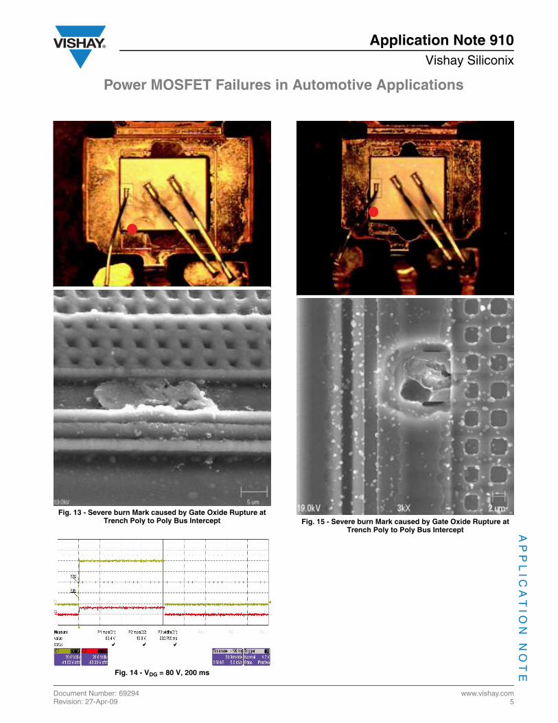
The transient test pulse definition and the correspondingfailure analysis are shown in figures 8 to 13. The transientwith open drain, VGS = 100 V, and 150 µs duration producesa failure signature close to field failure. Compare figures 17and 7.
Four more samples were tested to establish repeatability.Results are shown in figure 18 to 25. We can observe thatrepeatability can be established to the extent that the failuresignature is similar. However, the failure location varies.
Conclusions
While in actual application tests it seems almost impossibleto realize a VGS = 100 V, 150 µs pulse, the comparability ofthe signature confirms that a similar high-voltage transientdoes appear to create the failure. Although there is not adefinite solution to the problem of these low-ppm failures,there are actions which can be taken to further reduce thepotential for failure:
(1) The MOSFET manufacturer can increase the designmargins while implementing improved techniques andnew-generation materials. The attempt is to design andmanufacture a more rugged part that can sustain suchtransients. These are long term solutions, requiringextensive evaluation and qualification.
(2) The application system design can increase the electricaldesign margins to decrease the probability ofdevice-damaging transients reaching the powerMOSFETs.
(3) The handling environments for devices can bere-evaluated to eliminate the potential for ESD damage(from equipment or humans).
Fig. 1 - Power MOSFET in a Typical Battery Connect/Disconnect Application
Fig. 2 - Typical Failure Locations gate Metal to Drain Poly Short are located on the Periphery of the Device
U1
High-Side
D
1
G2
S
3
V_BAT
0
L1
1
2
L2
1
2
LN
1
2
D1 D2 DN
U2
Low-Side 1
D
1
G2
S
3
U3
Low-Side 2
D
1
G2
S
3
UN
Low-Side N
D
1
G2
S
3A
SIC
Con
trol
ler

Power MOSFET Failures in Automotive Applications
Application Note 910Vishay Siliconix
Document Number: 69294 www.vishay.comRevision: 27-Apr-09 3
AP
PL
ICA
TIO
N N
OT
E
Fig. 3 - An Example of a Field return: Gate Metal to Drain Poly Short - Top View
Fig. 4 - An Example of a Field return: Gate Metal to Drain Poly Short - X Section Short - Top View
Fig. 5 - Possible Failure Locations of Source Metal to Gate Poly Short
Fig. 6 - An Example of a Field return: Source Metal to Gate Poly Short - Top View
GateMetal
Drain Poly

Power MOSFET Failures in Automotive Applications
www.vishay.com Document Number: 692944 Revision: 27-Apr-09
Application Note 910Vishay Siliconix
AP
PL
ICA
TIO
N N
OT
E
Fig. 7 - Another Example of a Field return: Source Metal to Gate Poly Short - Top View
Fig. 8 - ESD Failure to Human Body Model. Gate/Drain/Source Short
Fig. 9 - ESD Failure to Machine Model. Gate/Drain/Source Short
Fig. 10 - ESD Failure to Machine Model. Gate/Drain/Source Short
Fig. 11 - ESD Failure to Machine Model. Gate/Source Short
Fig. 12 - VGS = 60 V, 4.5 ms
Power MOSFET Failures in Automotive Applications
Application Note 910Vishay Siliconix
Document Number: 69294 www.vishay.comRevision: 27-Apr-09 5
AP
PL
ICA
TIO
N N
OT
E
Fig. 13 - Severe burn Mark caused by Gate Oxide Rupture at Trench Poly to Poly Bus Intercept
Fig. 14 - VDG = 80 V, 200 ms
Fig. 15 - Severe burn Mark caused by Gate Oxide Rupture at Trench Poly to Poly Bus Intercept

Power MOSFET Failures in Automotive Applications
www.vishay.com Document Number: 692946 Revision: 27-Apr-09
Application Note 910Vishay Siliconix
AP
PL
ICA
TIO
N N
OT
E
Fig. 16 - Open Drain, VGS = 100 V, 150 µs
Fig. 17 - Severe burn Mark caused by Gate Oxide Rupture at Trench Poly to Poly Bus Intercept
Fig. 18 - Open Drain, VGS = 100 V, 120 µs
Fig. 19 - Severe burn Mark caused by Gate Oxide Rupture at Trench Poly to Poly Bus Intercept

Power MOSFET Failures in Automotive Applications
Application Note 910Vishay Siliconix
Document Number: 69294 www.vishay.comRevision: 27-Apr-09 7
AP
PL
ICA
TIO
N N
OT
E
Fig. 20 - Open Drain, VGS = 100 V, 115 µs
Fig. 21 - Severe burn Mark caused by Gate Oxide Rupture at Trench Poly to Poly Bus Intercept
Fig. 22 - Open Drain, VGS = 100 V, 110 µs
Fig. 23 - Severe burn mark caused by gate oxide rupture at trench poly to poly bus intercept

Power MOSFET Failures in Automotive Applications
www.vishay.com Document Number: 692948 Revision: 27-Apr-09
Application Note 910Vishay Siliconix
AP
PL
ICA
TIO
N N
OT
E
Fig. 24 - Open Drain, VGS = 100 V, 110 µs
Fig. 25 - Severe burn Mark caused by Gate Oxide Rupture at Trench Poly to Poly Bus Intercept