ST s MOSFET technologies for uninterruptible power supplies · ST’s MOSFET technologies for...
14
November 2013 DocID025494 Rev 1 1/14 AN4390 Application note ST’s MOSFET technologies for uninterruptible power supplies Introduction The UPS (uninterruptible power supply) is gaining ever increasing importance in office and industrial environments, because it preserves the information and business operations from power supply failure or blackout. Thanks to its technological improvement, it is now suitable both for big customers and for individual users. The right designer’s choice about MOSFETs in DC-AC (H-bridge converter) section enhances the overall system performance: THD, power and thermal management and short-circuit ruggedness. In this article, ST’s MOSFET technologies are described, highlighting their benefits as well. www.st.com
Transcript of ST s MOSFET technologies for uninterruptible power supplies · ST’s MOSFET technologies for...
November 2013 DocID025494 Rev 1 1/14
AN4390Application note
ST’s MOSFET technologies for uninterruptible power supplies
IntroductionThe UPS (uninterruptible power supply) is gaining ever increasing importance in office and
industrial environments, because it preserves the information and business operations from
power supply failure or blackout. Thanks to its technological improvement, it is now suitable
both for big customers and for individual users. The right designer’s choice about MOSFETs
in DC-AC (H-bridge converter) section enhances the overall system performance: THD,
power and thermal management and short-circuit ruggedness. In this article, ST’s MOSFET
technologies are described, highlighting their benefits as well.
www.st.com
Contents AN4390
2/14 DocID025494 Rev 1
Contents
1 Description . . . . . . . . . . . . . . . . . . . . . . . . . . . . . . . . . . . . . . . . . . . . . . . . . 3
2 MOSFET key parameters in UPS . . . . . . . . . . . . . . . . . . . . . . . . . . . . . . . 5
3 Technologies for UPS systems . . . . . . . . . . . . . . . . . . . . . . . . . . . . . . . . 6
3.1 STripFET IV DeepGATE technology . . . . . . . . . . . . . . . . . . . . . . . . . . . . . 7
3.2 STripFET VI DeepGATE technology . . . . . . . . . . . . . . . . . . . . . . . . . . . . . 9
4 Conclusions . . . . . . . . . . . . . . . . . . . . . . . . . . . . . . . . . . . . . . . . . . . . . . . 12
5 References . . . . . . . . . . . . . . . . . . . . . . . . . . . . . . . . . . . . . . . . . . . . . . . . 12
6 Revision history . . . . . . . . . . . . . . . . . . . . . . . . . . . . . . . . . . . . . . . . . . . 13

DocID025494 Rev 1 3/14
AN4390 Description
14
1 Description
Uninterruptible power supplies (UPS) are widely used to avoid a sudden loss of data or
information caused by a power supply disconnection (blackout). Power and voltage spikes,
supply frequency changes, noise and radio frequency interference affect negatively the
load. In Figure 1, the basic schematic of a "standby UPS" is shown; it is the most common
type of UPS present in the market [1]. Surge suppressor and input filter protect the output
equipment respectively from current spike and noise coming from input line. During an input
supply failure, the transfer switch enables the battery-powered path.
Figure 1. Standby UPS schematic
The UPS DC-AC section is formed by a H-bridge supplied by the battery voltage, which is
converted into a usable AC voltage for the output equipment (Figure 2).
Figure 2. DC-AC section: single-phase inverter
Q1-Q2 and Q3-Q4 are driven to allow current to flow through the load to both directions.
When Q1 and Q2 are in ON state, the voltage across the load is positive and the current
GIPD110920131644FSR
GIPD110920131649FSR

Description AN4390
4/14 DocID025494 Rev 1
flows from Q1 source to Q2 drain. Vice versa, when Q3 and Q4 are turned on, the voltage
becomes negative. Typical switching frequencies are in the range of 50-100 kHz. In
Figure 3, relevant gate signals for a H-bridge topology are showed.
Figure 3. MOSFET gate signals in H-bridge DC-AC converter
As per previous picture, when Q1 is turned off, the load current freewheels through Q4. In
this way, FETs of the same leg cannot be in ON state simultaneously avoiding any shoot-
through risk. Same considerations are valid during Q2 and Q3 switching. Together with
MOSFET power losses and efficiency analysis, evaluation tests on UPS systems include
two important tests:
• Short-circuit test: the output of DC-AC section is shorted for few seconds to test both
semiconductor cross-conduction robustness and system protection intervention.
• Back-feed test: back-feed protection prevents the electric shock from any electric
current feeding when a main supply fails.
GIPD120920131422FSR
DocID025494 Rev 1 5/14
AN4390 MOSFET key parameters in UPS
14
2 MOSFET key parameters in UPS
Power MOSFETs are key components for the UPS, because of their impact on DC-AC
section and on the whole system performance. Device’s features are below reported:
a) RDS(on): the major MOSFET loss in H-bridge configuration is the conduction loss,
because of the device’s on-time duration; so RDS(on)
optimization is mandatory for
the system efficiency enhancement.
b) Rth (thermal resistance): low Rth
values allow a good heat dissipation, reducing
the temperature.
c) VSD (body-drain diode forward voltage drop): during the freewheeling phase, the
current flows through body-drain diode, so the lower VSD
is, the lower diode losses
are.
MOSFET dynamic parameters (such as: gate charge and/or intrinsic capacitances) don't
play a crucial role in the device’s performance, due to low switching frequency values for
this kind of application. In UPS, typical MOSFET breakdown voltages are in the range of [55
V - 100 V], while most common package is TO-220.
Technologies for UPS systems AN4390
6/14 DocID025494 Rev 1
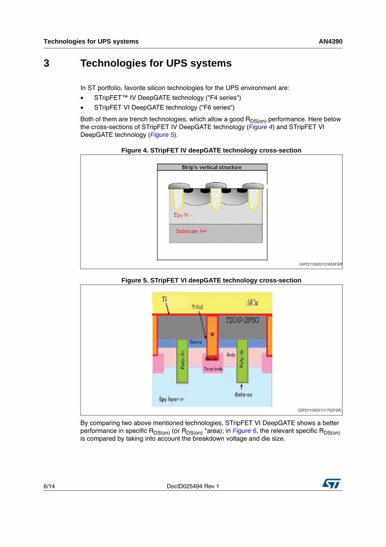
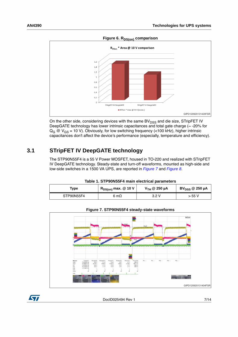
3 Technologies for UPS systems
In ST portfolio, favorite silicon technologies for the UPS environment are:
• STripFET™ IV DeepGATE technology ("F4 series")
• STripFET VI DeepGATE technology ("F6 series")
Both of them are trench technologies, which allow a good RDS(on)
performance. Here below
the cross-sections of STripFET IV DeepGATE technology (Figure 4) and STripFET VI
DeepGATE technology (Figure 5).
Figure 4. STripFET IV deepGATE technology cross-section
Figure 5. STripFET VI deepGATE technology cross-section
By comparing two above mentioned technologies, STripFET VI DeepGATE shows a better
performance in specific RDS(on)
(or RDS(on)
*area); in Figure 6, the relevant specific RDS(on)
is compared by taking into account the breakdown voltage and die size.
GIPD110920131653FSR
GIPD110920131702FSR
DocID025494 Rev 1 7/14
AN4390 Technologies for UPS systems
14
Figure 6. RDS(on) comparison
On the other side, considering devices with the same BVDSS
and die size, STripFET IV
DeepGATE technology has lower intrinsic capacitances and total gate charge (~ -20% for
QG
@ VGS
= 10 V). Obviously, for low switching frequency (<100 kHz), higher intrinsic
capacitances don't affect the device’s performance (especially, temperature and efficiency).
3.1 STripFET IV DeepGATE technologyThe STP90N55F4 is a 55 V Power MOSFET, housed in TO-220 and realized with STripFET
IV DeepGATE technology. Steady-state and turn-off waveforms, mounted as high-side and
low-side switches in a 1500 VA UPS, are reported in Figure 7 and Figure 8.
Figure 7. STP90N55F4 steady-state waveforms
GIPD120920131420FSR
Table 1. STP90N55F4 main electrical parameters
Type RDS(on) max. @ 10 V VTH @ 250 µA BVDSS @ 250 µA
STP90N55F4 6 mΩ 3.2 V > 55 V
GIPD120920131404FSR

Technologies for UPS systems AN4390
8/14 DocID025494 Rev 1
Figure 8. STP90N55F4 turn-off waveforms
The average power dissipation at turn-off is around 114 W, while the maximum
drain-source voltage spike is lower than 30 V. The STP90N55F4 has a good robustness
during short-circuit tests, when the UPS output is shorted for a fixed time. During a short-
circuit test, high-side and low-side gate-source voltages must not overlap to avoid the shoot-
through phenomenon. Figure 9 shows the screenshot, where yellow and blue traces are
low-side and high-side VGS
.
Figure 9. STP90N55F4 short-circuit waveforms
Another important feature for MOSFETs used in UPS is its ruggedness during back-feed
test (see Section 2: MOSFET key parameters in UPS). Figure 10 shows the UPS output
current, output voltage and AC main waveforms, when AC main voltage and UPS output
voltage are shifted 90°. The shortcut between AC main and output voltage (typically for a
hundred of ms) allows the user to check if the device passes the test without any failure.
GIPD120920131402FSR
GIPD120920131407FSR

DocID025494 Rev 1 9/14
AN4390 Technologies for UPS systems
14
Figure 10. STP90N55F4 back-feed test waveforms
3.2 STripFET VI DeepGATE technologyThe STP110N55F6 (STripFET VI DeepGATE) is tested in a 1500 VA UPS; below its main
electrical parameters. The high-side waveforms, during turn-on and off, are captured at
POUT
= 430 W (Figure 11 and Figure 12).
Figure 11. STP110N55F6 turn-on waveforms
GIPD120920131411FSR
Table 2. STP110N55F6 main electrical parameters
Type RDS(on) max. @ 10 V VTH @ 250 µA BVDSS @ 250 µA
STP110N55F6 4.3 mΩ 2.7 V > 55 V
GIPD120920131413FSR
Technologies for UPS systems AN4390
10/14 DocID025494 Rev 1
Figure 12. STP110N55F6 turn-off waveforms
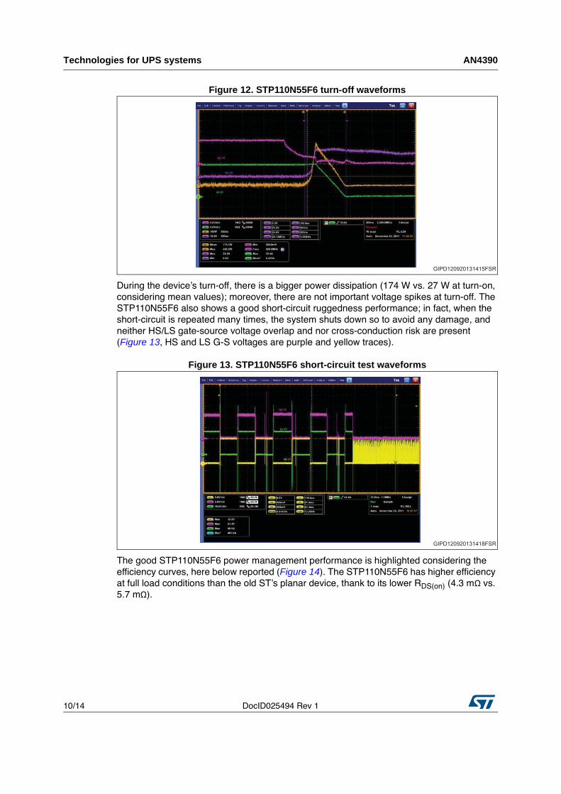
During the device’s turn-off, there is a bigger power dissipation (174 W vs. 27 W at turn-on,
considering mean values); moreover, there are not important voltage spikes at turn-off. The
STP110N55F6 also shows a good short-circuit ruggedness performance; in fact, when the
short-circuit is repeated many times, the system shuts down so to avoid any damage, and
neither HS/LS gate-source voltage overlap and nor cross-conduction risk are present
(Figure 13, HS and LS G-S voltages are purple and yellow traces).
Figure 13. STP110N55F6 short-circuit test waveforms
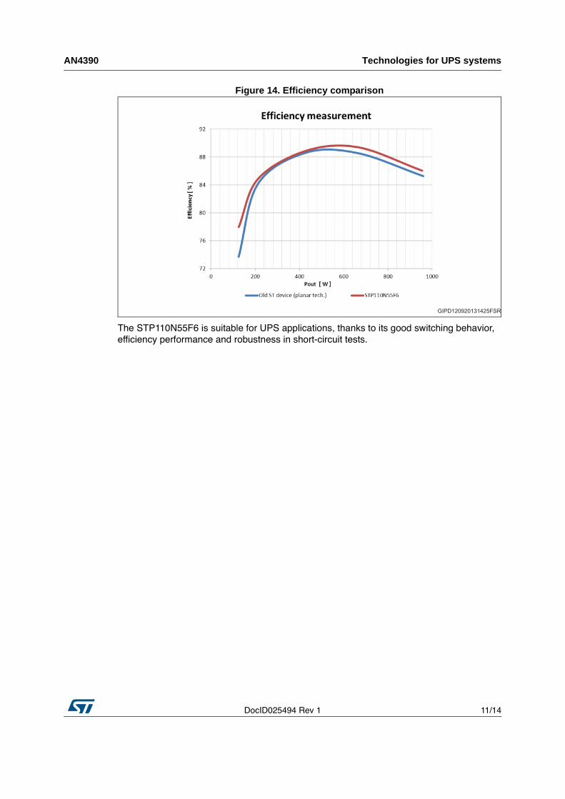
The good STP110N55F6 power management performance is highlighted considering the
efficiency curves, here below reported (Figure 14). The STP110N55F6 has higher efficiency
at full load conditions than the old ST’s planar device, thank to its lower RDS(on)
(4.3 mΩ vs.
5.7 mΩ).
GIPD120920131415FSR
GIPD120920131418FSR
DocID025494 Rev 1 11/14
AN4390 Technologies for UPS systems
14
Figure 14. Efficiency comparison
The STP110N55F6 is suitable for UPS applications, thanks to its good switching behavior,
efficiency performance and robustness in short-circuit tests.
GIPD120920131425FSR
Conclusions AN4390
12/14 DocID025494 Rev 1
4 Conclusions
The improvement of the UPS performance (THD, power management, short-circuit and
back feed test ruggedness, etc…) depends on the right design of DC-AC section. In this
document, ST’s trench MOSFET technologies (STripFET IV DeepGATE and STripFET VI
DeepGATE) are analyzed in 1500 VA UPS, showing a good switching behavior and power
management performance (any dangerous voltage spikes and/or cross-conduction risks)
and also passing short-circuit and back-feed tests without any failure. Both technologies are
hence suitable for high-side and low-side devices in DC-AC section of the modern UPS.
5 References
1. "An overview of uninterruptible power supplies", Racine M.S., Parham J., Rashid M.,
University of West Florida

DocID025494 Rev 1 13/14
AN4390 Revision history
14
6 Revision history
Table 3. Document revision history
Date Revision Changes
26-Nov-2013 1 Initial release.

AN4390
14/14 DocID025494 Rev 1
Please Read Carefully:
Information in this document is provided solely in connection with ST products. STMicroelectronics NV and its subsidiaries (“ST”) reserve the
right to make changes, corrections, modifications or improvements, to this document, and the products and services described herein at any
time, without notice.
All ST products are sold pursuant to ST’s terms and conditions of sale.
Purchasers are solely responsible for the choice, selection and use of the ST products and services described herein, and ST assumes no
liability whatsoever relating to the choice, selection or use of the ST products and services described herein.
No license, express or implied, by estoppel or otherwise, to any intellectual property rights is granted under this document. If any part of this
document refers to any third party products or services it shall not be deemed a license grant by ST for the use of such third party products
or services, or any intellectual property contained therein or considered as a warranty covering the use in any manner whatsoever of such
third party products or services or any intellectual property contained therein.
UNLESS OTHERWISE SET FORTH IN ST’S TERMS AND CONDITIONS OF SALE ST DISCLAIMS ANY EXPRESS OR IMPLIEDWARRANTY WITH RESPECT TO THE USE AND/OR SALE OF ST PRODUCTS INCLUDING WITHOUT LIMITATION IMPLIEDWARRANTIES OF MERCHANTABILITY, FITNESS FOR A PARTICULAR PURPOSE (AND THEIR EQUIVALENTS UNDER THE LAWSOF ANY JURISDICTION), OR INFRINGEMENT OF ANY PATENT, COPYRIGHT OR OTHER INTELLECTUAL PROPERTY RIGHT.
ST PRODUCTS ARE NOT DESIGNED OR AUTHORIZED FOR USE IN: (A) SAFETY CRITICAL APPLICATIONS SUCH AS LIFESUPPORTING, ACTIVE IMPLANTED DEVICES OR SYSTEMS WITH PRODUCT FUNCTIONAL SAFETY REQUIREMENTS; (B)AERONAUTIC APPLICATIONS; (C) AUTOMOTIVE APPLICATIONS OR ENVIRONMENTS, AND/OR (D) AEROSPACE APPLICATIONSOR ENVIRONMENTS. WHERE ST PRODUCTS ARE NOT DESIGNED FOR SUCH USE, THE PURCHASER SHALL USE PRODUCTS ATPURCHASER’S SOLE RISK, EVEN IF ST HAS BEEN INFORMED IN WRITING OF SUCH USAGE, UNLESS A PRODUCT ISEXPRESSLY DESIGNATED BY ST AS BEING INTENDED FOR “AUTOMOTIVE, AUTOMOTIVE SAFETY OR MEDICAL” INDUSTRYDOMAINS ACCORDING TO ST PRODUCT DESIGN SPECIFICATIONS. PRODUCTS FORMALLY ESCC, QML OR JAN QUALIFIED AREDEEMED SUITABLE FOR USE IN AEROSPACE BY THE CORRESPONDING GOVERNMENTAL AGENCY.
Resale of ST products with provisions different from the statements and/or technical features set forth in this document shall immediately void
any warranty granted by ST for the ST product or service described herein and shall not create or extend in any manner whatsoever, any
liability of ST.
ST and the ST logo are trademarks or registered trademarks of ST in various countries.
Information in this document supersedes and replaces all information previously supplied.
The ST logo is a registered trademark of STMicroelectronics. All other names are the property of their respective owners.
© 2013 STMicroelectronics - All rights reserved
STMicroelectronics group of companies
Australia - Belgium - Brazil - Canada - China - Czech Republic - Finland - France - Germany - Hong Kong - India - Israel - Italy - Japan -
Malaysia - Malta - Morocco - Philippines - Singapore - Spain - Sweden - Switzerland - United Kingdom - United States of America
www.st.com