Overview of Beyond-CMOS Devices and A Uniform Methodology ...
91
1 Overview of Beyond-CMOS Devices and A Uniform Methodology for Their Benchmarking Dmitri E. Nikonov and Ian A. Young Components Research, Intel Corp., MS RA3-252, 2501 NW 229th Ave., Hillsboro, OR 97124, email: [email protected] Ver. 3.4 09/21/2012 Abstract Multiple logic devices are presently under study within the Nanoelectronic Research Initiative (NRI) to carry the development of integrated circuits beyond the CMOS roadmap. Structure and operational principles of these devices are described. Theories used for benchmarking these devices are overviewed, and a general methodology is described for consistent estimates of the circuit area, switching time and energy. The results of the comparison of the NRI logic devices using these benchmarks are presented. Keywords – beyond-CMOS, logic, electronics, spintronics, integrated circuits, power dissipation, computational throughput, adder.
Transcript of Overview of Beyond-CMOS Devices and A Uniform Methodology ...

1
Overview of Beyond-CMOS Devices and A
Uniform Methodology for Their Benchmarking
Dmitri E. Nikonov and Ian A. Young
Components Research, Intel Corp., MS RA3-252, 2501 NW 229th Ave., Hillsboro, OR
97124, email: [email protected]
Ver. 3.4 09/21/2012
Abstract
Multiple logic devices are presently under study within the Nanoelectronic Research
Initiative (NRI) to carry the development of integrated circuits beyond the CMOS
roadmap. Structure and operational principles of these devices are described. Theories
used for benchmarking these devices are overviewed, and a general methodology is
described for consistent estimates of the circuit area, switching time and energy. The
results of the comparison of the NRI logic devices using these benchmarks are presented.
Keywords – beyond-CMOS, logic, electronics, spintronics, integrated circuits, power
dissipation, computational throughput, adder.

2
1. Introduction
The development of CMOS integrated circuits has had unprecedented success from the
scaling of its dimensions each new technology generation. Its further development is
charted over the next several years by the International Technology Roadmap for
Semiconductors [1] (ITRS). From the ITRS projections it transpires that the scaling will
be influenced by fundamental physical limits of device switching [2]. Due to this
observation, research thrusts in the academia and the industry (most prominently, the
Nanoelectronic Research Initiative - NRI) gained significant momentum towards
demonstrating and thoroughly investigating feasible alternatives to CMOS.
The NRI group has also performed benchmarking of the “beyond-CMOS” devices
[3]. Such an investigation is of utmost importance, since it permits identification and
focusing of resources on researching the most promising devices. However this
benchmarking investigation provided only a summary report of the results (e.g. Figure 1),
without providing a uniform common methodology and details behind the benchmarking
calculations needed to reproduce them. Also different investigators made sometimes
widely different assumptions regarding the operating conditions and characteristics of
individual devices. One of the main goals of this study was to obtain the values for the
area, switching time, and switching energy of a set of standard circuits – an inverter with
a fanout of 4, a 2-input NAND gate, and a 32-bit adder. We adopt the same goal in this
paper just to be able to make a one-to-one comparison. Such benchmarks are very useful
as they allowed for the first time a comparison of the promise of beyond-CMOS
computing with the mainstream, CMOS, computing. However one needs to be aware of
limitations of such an approach. It well may happen that a different circuit architecture
3
needs to be worked out for optimal performance of beyond-CMOS devices. For example,
spintronic devices are non-volatile (preserve their state when the power is switched off),
and a different circuit is needed to make use of its property to create normally-off
instantly-on logic chips. Present benchmarks are not designed to measure this utility of
devices. Moreover, different devices may prove to be best suited for different roles within
a circuit. We conjecture that future integrated circuits will still contain a majority of
CMOS devices with a few other beyond-CMOS devices performing various specialized
functions. Also by focusing on the switching energy, one comprehends only the active
power dissipation, but not the standby (“leakage”) power. Such benchmarks need to be a
subject of future research.
In this paper we are setting out to establish a consistent standard methodology for
benchmarking beyond-CMOS logic devices in order to obtain a reliable set of metrics
and fair comparison of these devices. In treatment of the devices we chose simplicity
rather than rigor. Wherever possible, we used analytical expressions, rather than
simulations, for calculations of benchmarks. At the present time the structure of the
devices and their operational characteristics are not firmed up. We believe it
presumptuous at this early stage of the research to expect the benchmarks to be accurate
within less than a factor of 2. We strived for uniformity of benchmarking: same
assumptions, relations, and schemes are applied to all devices to which they may pertain.
Therefore the relative benefits of the devices under study might be more accurate than
their absolute values. We also insisted on complete transparency of our benchmarks. All
the equations and parameters used are listed in this paper. We provide the Matlab code
used to generate all plots in this paper [4]. This way the readers can reproduce all the

4
results of the paper. Also they can plug in their values and assumptions and explore
“what if” scenarios.
Figure 1. Comparison of devices from K. Bernstein’s presentation [5].
The paper is structured as follows. The requirements of logic technologies are
outlined in Section 2. Non-traditional computational variables are described in Section 3.
The nomenclature of beyond-CMOS devices is introduced in section 4. Physical
constants and device parameters are listed in Section 5. The principles of layout and
assumptions about the gate size are described in Section 6. The method used for
estimating the circuit area is explained in Section 7. General considerations for time and
energy of capacitance charging are considered in Section 8. Simple analytical expressions
for the switching time and energy of electronic circuits are proposed Section 9. Estimates

5
for various methods of magnetization switching are collected in Section 10. Section 11
contains the estimates of performance for spintronic devices. Overall benchmarks for
devices are compared in Section 12. The consequences for the computational throughput
and dissipated power are calculated in Section 13. The results of the paper are discussed
in Section 14.
In this paper we limit the scope to only digital circuits. We do not consider analog,
mixed or digital-to-analog conversion circuits. Moreover we only consider Boolean logic,
thereby excluding non-Boolean [6] or neuromorphic [7] computing.
2. Tenets of logic and device interconnection
Before it can be considered as a candidate for an element of an integrated logic circuit, a
solid-state device needs to satisfy a set of requirements [8], “logic tenets”, such as:
i. Non-linear characteristics (related to noise margin and the signal-to-noise ratio)
ii. Power amplification (gain>1)
iii. Concatenation (output of one device can drive another)
iv. Feedback prevention (output does not affect input)
v. Complete set of Boolean operators (NOT, AND, OR, or equivalent)
In addition it needs to be competitive in the quantitative physical measures of:
i. Size (i.e. scalability)
ii. Switching time
iii. Switching energy (i.e. power dissipation)
And finally, technological requirements, such as
i. Room temperature or higher operation

6
ii. Low sensitivity to parameters (e.g. fabrication variations)
iii. Operational reliability
iv. CMOS architectural compatibility (interface, connection scheme)
v. CMOS process compatibility (fabricated on the same wafer)
vi. Comprehending intrinsic and extrinsic parasitic and their interface to interconnect
may decide the fate of a device in the competition to be the next technology of choice.
Devices considered in this study are at various levels of technological maturity. Some
have been demonstrated experimentally, operation of others has been simulated, while
some are still at the concept stage. In this paper we do not review the status of
experimental work of the devices or discuss the issues of their manufacturability. Neither
are we trying to predict the success of their integration to logic circuits. We assume that
devices would work as they are intended and estimate their performance characteristics
starting from physical relations governing phenomena underlying them. We make
optimistic assumptions about the material parameters, lithography capabilities, and
device structures without pushing these values to their physical limits.
3. Computational variables and device classification
The beyond-CMOS devices encode information by various physical quantities, which we
call “computational variables”. A list and a pictorial representation of types of
computational variables are shown in Figure 2. We use them to classify devices.
The first set of variables comprises charge, current, and voltage (designated as Q, I, and
V, respectively). It is very familiar to the readers, is the underlying group of variables in
electronic devices, which comprise the overwhelming majority of mainstream computing

7
and a few beyond-CMOS options. Ferroelectric devices are based on electric dipoles
(designated as P). Ferroelectric transistors [8] have been researched and demonstrated for
many years now, and we do not include them in this study. Spintronic [9] devices [10]
rely on magnetic dipoles represented by ferromagnetic elements or electrons with
polarized spins (designated as M). Orbitronic devices are the least understood ones, as
they involve the orbital state (designated as Orb) of electrons in a molecule or a crystal,
and sometimes a collective state of electrons, such as Bose condensate of excitons
(designated as Cond). In the current study they are represented by a single device, the
BisFET. There are other computational variables, described in the ITRS [1] ERD chapter,
such as: mechanical position for NEMS devices, light intensity for photonic devices,
timing of signals in neuromorphic computing, etc. But they are not used in this study.
Figure 2. Scheme of computational variables.
The computational variables can have various roles in a logic circuit. To explain
them, we envision a very abstract black-box diagram of a logic device shown in Figure 3.
The computational variables encode the internal state, input and output signals and the
controls for switching devices (including clocking).

8
Figure 3. Black-box diagram of a device.
One of the tenets of logic (in Section 2) is that the output of one stage needs to be able to
drive the input to the next stage. If this condition is not satisfied for a device, e.g. the
input is a voltage signal but the output is a magnetization signal, special purpose devices
which we call “transducers”, are needed to convert one variable to another. The most
important transducers discussed below are the ones converting electronic signals to
spintronic ones and vice versa.
4. Nomenclature and short description of the devices
Devices are classified according to their computational variables as they represent inputs,
outputs, and the internal state (Section 3) when the devices are connected in an integrated
circuit, see Table 1. The subclass is assigned according to a phenomenon underlying the
device operation. This is explained in more detailed as we go over devices one-by-one.
We aim to give a very short description of a device features and nature of connections
relevant for our discussion.
Device name acronym input
control int. state
output
class subclass
Si MOSFET high performance CMOS HP V Vg Q V electronic barrier
Si MOSFET low power CMOS LP V Vg Q V electronic barrier
Homojunction TFET HomJTFET V Vg R V electronic tunneling
Heterojunction TFET HetJTFET V Vg R V electronic tunneling
Graphene nanoribbon TFET gnrTFET V Vg R V electronic tunneling

9
Graphene pn-junction (Veselago) GpnJ V Vg R V electronic refraction
Bilayer pseudospin FET BisFET V Vg BEC V orbitronic exciton
SpinFET (Sughara-Tanaka) SpinFET V Vg, Vm Q, M V spintronic spin drift
Spin torque domain wall STT/DW I V M I spintronic domain wall
Spintronic majority gate SMG M V M M spintronic domain wall
Spin torque triad STTtriad I V M I spintronic nanomagnet
Spin torque oscillator STOlogic I V M I spintronic nanomagnet
All spin logic device ASLD M V M M spintronic spin diffusion
Spin wave device SWD M I or V M M spintronic spin wave
Nanomagnetic logic NML M B or V M M spintronic nanomagnet
Table 1. Nomenclature and classification of included devices.
4.1 CMOS.
The complementary metal-oxide-semiconductor (CMOS) FET (Figure 4) is a familiar
device. Its internal state is a charge on the capacitor of the gate dielectric. The input and
gate voltages determine the output voltage (Figure 5). Switching is done by raising and
lowering of the potential barrier for electrons in the channel due to a change of the gate
voltage. For high performance CMOS (CMOS HP) we use the values from the 2011
edition of ITRS [1] PIDS chapter. There the technology node F=15nm, chosen for the
NRI study, corresponds to the 2018 column. The low-power CMOS (CMOS LP) used in
the NRI benchmarking study is envisioned as a low supply voltage (0.3V) device from
[11]. It is to be noted that it is different from the low operating power (LOP CMOS) and
low standby power (LSP CMOS) transistors considered in ITRS [1].

10
Figure 4. Advanced Si multi-gate MOSFET according to [1]. The scheme is be used
for both high-performance and low-power CMOS, depending on the applied and
threshold voltages.
Figure 5. Block-diagram for CMOS.
4.2. Tunneling FET.
Tunneling field-effect transistors (TFET) [12] are considered under three material options
– homojunction III-V material (HomJFET, Figure 6) specifically InAs double-gate
transistor, heterojunction III-V material [13] (HetJFET, Figure 7) specifically InAs/GaSb
double-gate transistor, and graphene nanoribbon (gnrFET, Figure 8). They have the same
principle of operation and differ in performance parameters - supply voltage and drive
current. Parameters for TFET are taken from simulation, such as [14]. Conduction in a
TFET occurs through band-to-band tunneling (BTBT). Gate voltage shifts the bands in

11
energy and drastically changes the probabilities of tunneling. The block-diagram of TFET
(Figure 10) is very similar to that of CMOS. Simulations show that charge on a gate of
the TFET is smaller than the corresponding CMOS [15]. Therefore we prefer to associate
the state of the device with the resistance of the channel (R). Besides, this smaller gate
capacitance contributes to faster switching of circuits, an advantage of TFET beyond just
comparing drive currents.
Figure 6. III-V Homojunction Tunneling FET (HomJTFET)
Figure 7. Heterojunction (HetJTFET)
Figure 8. Graphene nanoribbon (gnrTFET)

12
4.3 Graphene pn-junction.
A graphene pn-junction (GpnJ, Figure 9) [16] device uses the junctions to switch the path
of electrons. It shares the block-diagram with the TFET (Figure 10) signifying the change
of the resistance as an internal state, but relies on a completely different physical
phenomenon. Reflection of electrons from pn-junctions in graphene is highly dependent
on the angle due to its peculiar bandstructure. Therefore, by switching the electrostatic p
and n doping of graphene by applying voltage to electrodes, it is possible to achieve
either a very high transmission or a total internal reflection of electrons. Thus current is
directed to one vs. another output of the device.
Figure 9. Graphene pn-junction (GpnJ)
Figure 10. Block-diagram for tunneling transistors and graphene pn-junctions.
4.4 BisFET.
A bilayer pseudospin FET (BisFET, Figure 11) [17] is another graphene device. It
exploits tunneling between two monolayers of graphene. Due to a stronger interaction of
electrons and holes in graphene, it is expected that they will bind into excitons at a higher

13
temperature than in traditional semiconductors. If holes are injected into one monolayer
and electrons into another monolayer, they may bind into excitons and these excitons
might relax into a Bose-Einstein condensate (BEC) state. Considerable controversy exists
about the critical temperature of BEC in bylayer graphene: the original proposal [18]
suggest that it is above room temperature, while subsequent calculations [19] predict that
it is much lower than 1K. The presence of BEC is expected to drastically increase the
probability of tunneling due to its collective nature. BEC state can be destroyed due to
changing the balance between electrons and holes by applying a gate voltage. Thus
voltage controls the internal state (R) of the device related to the presence of the
condensate, see Figure 12. The current between source (S) and drain (D) in Figure 11 is
expected first to grow with the increase of voltage Vds and then decrease as the carrier
imbalance destroys BEC (thus exhibiting negative differential resistance). The device
proposal [17] postulates the current-voltage (I-V) curve with a peak at voltage of 5mV.
For the present benchmarks we are using the results of quantum transport simulations
[20,21,22] which exhibit I-V curves with peak voltages of 150mV to 400mV. Though
they were performed for a different value of the interlayer coupling constant and different
wiring of the device. The gates V(+) and V(-) are designed to maintain certain high
densities of electrons and holes in the bottom and top graphene layers, respectively.
These potentials need to be kept constant. Gate G covers only a half of the channel and is
used to control the BisFETs in logic circuits. Its indended use is “current crowding”: the
applied voltage causes current to flow on one side of the channel. If current density there
exceeds the peak value, conduction there drops, and the current is forced to the other side
and it exceeds the peak current density there as well.

14
Figure 11. Bilayer pseudospin (BisFET) scheme [23].
Figure 12. Block-diagram for BisFET.
4.5. SpinFET.
A spinFET (Figure 13) [24] combines a MOSFET and a switchable magnetic element. Its
source and drain are made of ferromagnetic metals and another ferromagnet is positioned
over a drain in order to detect its direction of magnetization via a tunneling
magnetoresistance (TMR) effect. In addition to the usual FET functionality, R(Q), the
resistance of a spinFET depends on the magnetization state, R(M), see Figure 14. If the
magnetizations of the source and drain are parallel, the resistance of the channel is low. If
they are anti-parallel, the resistance is high. In addition to the current through the

15
channel, the magnetization of the drain can be switched by a current from a terminal
controlled by voltage Vm.
Figure 13. SpinFET (Sughara-Tanaka) [25].
Figure 14. Block-diagram for SpinFET.
4.6. Spintronics features.
As in most of the spintronic devices, the Magnetic Tunnel Junction (MTJ) is required
only at the output magnets in order to detect the direction of magnetization. MTJ is a
stack of a ferromagnet, a tunneling dielectric, and another ferromagnet. It has a huge
advantage in the values of magnetoresistance (MR) compared to spin valves, but at the
price of around three orders of magnitude higher resistance-area product. A spin valve is
a stack of a ferromagnet, a non-magnetic metal, and another ferromagnet. When only a

16
switching based on the spin torque principal is required, a spin valve is preferable and
gives a comparable polarization of the spin current.
Most of the spintronic devices are non-volatile, i.e. their computational state is
preserved even when the power to the circuit is turned off. The condition for non-
volatility is stability of nanomagnets against thermal fluctuations. In other words, the
magnet should have two states of equilibrium separated by a barrier with energy greater
than 60kBT.
4.7. Spin transfer torque domain wall device.
A spin transfer torque / domain wall (STT/DW) device (Figure 15) [26] operates by
motion of a domain wall in a ferromagnetic wire. The motion is caused by a spin transfer
torque effect of a current along the wire (unlike a current perpendicular to the wire used
in the rest of the spin torque devices in this paper). As the domain wall moves, the
magnetization below the MTJ stack (in the middle of the device) switches, resulting in
high or low resistance of the stack. Then a current from the “clock” terminal to the output
through the MTJ is either high or low. The current is used to drive the inputs of next
stages (Figure 22).

17
Figure 15. Spin transfer torque domain wall logic (STT/DW). A domain wall
separates regions with opposite magnetization (shown as red and blue).
4.8. Spintronic majority gate.
A spintronic majority gate (SMG, Figure 16) [27,28] is implemented with a “cross” of
ferromagnetic wires. It has three inputs and one output terminals formed over the ends of
the “cross” as nanopillars with their own ferromagnetic layer. Current from each
nanopillar exerts spin torque which aims to switch magnetization to a certain direction,
depending on the sign of the current. The majority of the inputs win and enforce their
direction of the magnetization. This is sensed via the Tunneling Magnetoresistance
(TMR) effect using a sense amplifier (Figure 23). Like a few other spintronic devices,
inputs can be switched and outputs can be sensed by a magnetoelectric (ME) cell (rather
than spin torque and TMR), see Figure 24. For the principle of operation of a ME cell,
see Section 10. It should be noted that electric-spin conversion (= writing and sensing of
magnetization) does not need to occur at every majority gate input/output. Instead
multiple majority gates can be cascaded into a larger magnetic circuit. For example, three

18
majority gates are enough to form a one-bit full adder. Electric-spin conversion then
happens only at the adder interface between the magnetic and the electronic circuits.
Figure 16. Spintronic majority gate (SMG).
4.9 Spin transfer torque triad.
A spin transfer torque triad (STTtriad) [29] element works in a manner similar to the
SMG. However it consists of triangular structures (Figure 17) with two inputs and one
output. Then the current from one triangle is used to drive spin torque switching in other
triangles, in a manner similar to STT/DW (Figure 22). This geometry implies electric-
spin conversion at every computing element, rather than cascading magnetic signals.
Output
MTJ stack
Input
MTJ stack

19
Figure 17. Spin transfer torque triad (STTtriad) [29].
4.10. Spin torque oscillator logic.
Spin torque oscillator (STO) logic [30] contains oscillators which are driven by spin
torque from currents entering each of them through nanopillars on top (Figure 18). STOs
are combined into a majority gate with three input and one output oscillator. The
oscillators have a common ferromagnetic layer, similar to SMG. Oscillations cause spin
waves to propagate in the common layer and thus the oscillators’ signal couple. The
frequency of the output oscillator is determined by the majority of inputs and serves as
the logic signal in the circuit. By the nature of the signals, STO logic is described by the
block diagram in Figure 22. Since in order to oscillate the STOs must have only one
position of equilibrium, therefore this type of logic is volatile.

20
Figure 18. Spin torque oscillator (STO) logic
4.11. All spin logic.
An all spin logic device (ASLD) [31, 32] is formed by nanomagnets placed over a copper
wire (Figure 19). Each nanomagnet has an input and the output sides separated by an
insulator. Voltage supplied to the top of each nanomagnet drives a current to the ground
terminal nearby. Due to this current spin polarized electrons accumulate near each
nanomagnet. Concentrations of polarized spins are different at the input and output sides
of the two neighboring magnets, which causes a diffusion spin current to occur. This spin
current exerts torque on a nanomagnet and is able to switch its polarization. The
nanomagnets are often arranged into majority gates. The nanomagnets can be
concatenated according to the block-diagram in Figure 23, for example, to produce a one-
bit full adder, as in Figure 19.

21
Figure 19. All spin logic devices (ASLD) forming a one bit of a full adder [33].
4.12. Spin wave device.
A spin wave device (SWD, Figure 20) [34, 35] contains nanomagnets connected by
ferromagnetic wires. Spin waves are excited in the wires and propagate along them. Short
pulses of spin waves containing a wide range of frequencies are used. There are two
versions of the device in which: 1) spin waves are excited and detected by an RF antenna;
this version does not need nanomagnets and is volatile, corresponding to the scheme in
Figure 23; 2) spin waves are excited and detected by a magnetoelectric cell; it includes
nanomagnets and is non-volatile, corresponding to the scheme in Figure 24. The
magnetization of a nanomagnet determines the phase of the spin wave at a given
coordinate. In its turn, this phase determines to what direction magnetization will switch
in the output nanomagnet. SWD gates are readily amenable to cascading.

22
Figure 20. Spin wave device (SWD).
4.13. Nanomagnetic logic.
Nanomagnetic logic (NML, Figure 21) [36] consists of a chain of nanomagnets. They
interact by magnetic dipole coupling. NML is the only device in the NRI suite of
spintronic devices which uses Bennett clocking [36]. In other words, its operation occurs
by preparing all nanomagnets in a quasi-stable equilibrium state by the action of a
magnetic field from a current in a wire (current clocking, Figure 23) or effective
magnetic field from the charging a magnetoelectric cell (voltage clocking, Figure 24). In
both cases the state of magnets at the input causes the magnets in the circuit to choose
one of the stable equilibrium states determined by the dipole interaction between
magnets. It is easy to cascade NML gates.

23
Figure 21. Nanomagnetic logic (NML).
Figure 22. Block-diagram for STT/DW, STOlogic, and STTtriad driven by spin
torque.
Figure 23. Block-diagram for SMG, ASLD, SWD, and NML driven by spin torque.

24
Figure 24. Block-diagram for SMG, ASLD, SWD, and NML with magnetoelectric
switching.
4.14. Other devices.
Beyond-CMOS devices previously considered within the NRI studies or in other research
overviews that are not included in this study are: Datta-Das spin modulator [37],
electronic ratchet [38]; graphene thermal logic [39]; SET/BDD [40]; electron structure
modulation transistor [41]; RAMA [42,43]; resonant injection enhanced FET [44];
magnetic domain-wall Logic [45]; domain wall majority gate logic [46]; MottFET [47];
spin Hall effect transistor [48]; few spin device [49]; magnetic tunnel junction (MTJ) plus
CMOS logic [50,51,52,53]. We also do not cover the optoelectronic excitonic transistor,
which was demonstrated [54,55,56], as well as other proposed versions of excitonic FETs
[3,57,58]. The reason for non-inclusion is either lack of input information to build
benchmarks or insufficient research activity on this device at NRI.
5. Constants and parameters
In the estimates of the device performance we are using the following constants and
parameters collected in Table 2 and Table 3.
.
PHYSICAL QUANTITY SYMBOL UNITS VALUE

25
Electron charge, absolute value e C 1.602176565e-19
Electron mass em kg 9.10938291e-31
Planck’s constant J*s 1.054571726e-34
Permittivity of vacuum 0 C2/(J*m) 8.854187817e-12
Speed of light c m/s 2.99792458e8
Boltzmann’s constant Bk J/K 1.3806488e-23
Permeability of vacuum 0 kg*m/ C2
2 1
0( )c
Lande factor g 2
Bohr magneton B A*m2 /(2 )ee m
Gyromagnetic constant C/kg /(2 )ege m
Quantum resistance qR 22 / e
Table 2. Fundamental physical constant used in the analysis.
PHYSICAL QUANTITY SYMBOL UNITS TYPICAL VALUE
Ambient temperature T K 300
Dielectric constant of SiO2 3.9
Dielectric constant of interlayer dielectric ILD 2
Particle velocity in graphene Fv m/s 8e5
Resistivity of copper *m 1.9e-8
Magnetization in a ferromagnet, in plane sM A/m 1e6

26
Magnetization in a ferromagnet,
perpendicular spM A/m 0.3e6
Injected spin polarization P 0.8
Gilbert damping 0.01
Perpendicular magnetic anisotropy uK J/m3 6e5
Current density for domain wall motion dwJ A/m2 1.4e11
Magnetic permeability around wires 4
Magnetic induction from a wire, required wiB
T 0.01
Multiferroic electric polarization [59] mfP C/m2 0.55
Multiferroic switching field [59] mfE V/m 2e7
Multiferroic exchange bias mfB T 0.03
Magnetostrictive switching field [60] msE V/m 6e5
Magnetostrictive effective field [61] msB
T 0.03
Dielectric constant of piezoelectric [60] ms
20000
Magnetoelectric coefficient [62] me
s/m 5.6e-9
Dielectric constant of magnetoelectric me
1000
Table 3. Material constants used in the analysis.
6. Layout principles
In this section we propose a simple but general method to estimate the areas of
beyond-CMOS circuits. The semiconductor process generations are labeled by

27
characteristic lithography size called the DRAM’s half-pitch, F . It is set to 15nm in this
study. ITRS [1] projects values of many device parameters depending on F . We use the
following device parameters in Table 4.
PHYSICAL QUANTITY SYMBOL UNITS TYPICAL VALUE
Gate length gL m 1.28e-8
Equivalent oxide thickness, nominal EOT0 m 0.68e-9
Equivalent oxide thickness, electrical EOT m 1.08e-9
Contact resistance cR *m 1.6e-4
Contact capacitance cC F/m 1.2e-10
Magnetic induction to switch NML ndB T 0.01
Ferromagnet thickness fmd m 2e-9
Piezoelectric thickness for
magnetoelectric effect med m 25e-9
Table 4. Device parameters used in the analysis.
The layout of the devices is governed by the design rules which specify minimum width
and spacing of various elements in the circuit [63]. Scalable design rules are formulated
in units of maximum mask misalignment , [63], where typically / 2F . An example
of design rules is shown in Figure 25.

28
Figure 25. Example of scalable design rules for a CMOS foundry.
Figure 26. Layout of a transistor, after [64].
We see in Figure 26 that the pitch of metal-1 in the contacted transistor is 8mp .
On the other hand, the metal 1 contacted gate pitch scales with the process generation
[65], see Figure 27.

29
Figure 27. Contacted transistor metal-1 pitch in various process generations [65].
From this plot we approximately obtain that the metal 1 pitch is 4mp F . This confirms
the previous relation 2F . Since all the logic circuits (even spintronics circuits) need
electric contacts at the terminals of gates, their size will be determined by the
metallization pitch much more than by their intrinsic device sizes. We proceeds to draw
layouts for simple circuits for all of the considered devices in the following section. We
are using the color scheme shown in Figure 28 to designate mask layers. We notices that
their area can be estimated by counting the pitches of the most important lines (diffusion,
gate (“poly”), metal 1) [64] as shown in Figure 29. Here and in the rest of the document,
one cell of the grid corresponds to size . The contacted pitch for all these important lines
proves to be 8 . Thus in the rest of the paper we take the minimum pitch between any
contacted circuit elements to be 8 4F .

30
Figure 28. Legend for the layout layers used in this paper.
Figure 29. Layout and area estimation for a CMOS inverter and a 2-input NAND
gate.
7. Circuit area estimation
We use the parameters in Table 5 to calculate the sizes of devices and circuits.

31
PARAMETER TYPICAL VALUE
Transistor width Xw / F 4
Spin contact width Sw / F 1
Width of metal-1 mw / F 2
Height of metal-1 mp / F 4
Separation of metal-1 lines ms / F 2
Interlayer -1 thickness dd / F 4
Inverter FO1 length and width / pitch 2 x 5
NAND2 length and width / pitch 3 x 6
XOR area / NAND2 area 2
Gate area overhead, gateM 1.5
Bit area overhead, bitM 1.5
Adder area overhead, addM 1.5
Interconnect length / pitch 5
Table 5. Geometry parameters of the devices.
The size of the intrinsic device (a transistor-like device has subscript X, and a spintronic
device has subscript S) is obtained as
int / 2 2X S ma w F p F . ( 1 )

32
7.1. Area of transistor-like devices
First we deal on the same footing with the area estimates of transistor-like devices
(CMOS HP, CMOS LP, HomJTFET, HETJTFET, gnrTFET, BisFET, SpinFET)
and the area of the STT/DW, which all have the same or similar circuit architecture.
The sizes of the inverter with fanout 4, 2 input NAND fanout-1, and 2 input XOR fanout-
1 gates are calculated using the factors in Table 5, which are derived from layout
diagrams. The interconnect length is important for calculating its capacitance and is
estimated as
5ic ml p .
( 2 )
This interconnect’s area is not an additive term in the area calculation of the circuits,
since it is positioned in the metal-1 layer. However, when interconnect area is needed to
properly route interconnects, we account for the extra empty area needed around the gates
and 1-bit adder cells by introducing the empirically derived area overhead factors listed
in Table 5. These factors work as follows. The area of a gate is obtained by estimating the
gate length and width of the layout cell, and then multiplying it by the gate overhead
factor. We assume that the inverter is made with the standard transistor width Xw . We
take the n- and p-transistors to be of the same width due to an assumption of them having
approximately equal on-current. The usual electrode pitch would accommodate
transistors of width Xw . Extra width of transistors results in an increase of the gate area.
So for the fanout-4 inverter its area is (Figure 29)

33
4 2 3 2inv m m X gatea p p w M . ( 3 )
For the NAND2 gate, we make the width of transistors in the pull-down network (nFET
in this case) to be twice the standard width. Thus the area of fanout 1 two-input NAND is
(Figure 29)
3 3 3nand m m X gatea p p w M . ( 4 )
Figure 30. Layout and area estimation for a TFET inverter and a 2-input NAND
gate.
A tunneling FET needs to have the source and drain to have doping of opposite polarities
close to each other. That would violate the traditional scalable CMOS design rules related
to p-doped diffusion in an n-well (as we show in Figure 30). We adopt a new design rule
of minimum spacing of 2 between n- and p-diffusion. Thus a new process flow needs to
be developed. Also TFETs commonly have gate-drain underlap [11], which we set at the
most stringent value of 2. [Note that a version of a layout of vertical TFET performed

34
according scalable MOS design rules was shown in [66]]. With these two changes, the
inverter for TFET has the same area as CMOS, while the area of NAND2 is increased to
, 4 3 3nand tfet m m X gatea p p w M . ( 5 )
In spite of the fact of an addition of a magnetic tunnel junction, the size of the SpinFET
cell is the same as that of CMOS, see Figure 31.
….
Figure 31. Layout and area estimation for a SpinFET inverter and a 2-input NAND
gate.
The layouts of BisFET circuits, according to the scheme in Figure 12, are shown in
Figure 32. It is apparent that the area for BisFET circuits is larger due to many additional
electrodes.

35
Figure 32. Layout and area estimation for a BisFET inverter and a 2-input NAND
gate.
The scheme of a 1-bit of a full adder [67] (Figure 33) shows that it consists of 2 XOR-
gates with two inputs and 3 AND/OR gates with two inputs, and thus its area is
approximately
1 2 2xor nand bita a a M . ( 6 )
We approximately set the XOR area to 3xor nanda a . Note that the circuit diagram of a
BisFET-based adder, Figure 34, (despite a different principle of device operation) has in
essence the same structure and is therefore treated on the same footing.
Figure 33. Transistor-like adder block diagram [67].

36
Figure 34. Bilayer pseudospin (BisFET) adder block diagram [68].
The area of the full 32 bit adder is calculated as
32 132 adda a M . ( 7 )
Figure 35. Layout and area estimation for a STT/DW 2-input AND/OR gate.
7.2. Area of STT/DW
The structure of STT/DW is somewhat different and presents a special case. Three
independent electrodes (two inputs and one output) are required for one device which
represents a NAND gate (Figure 15 and Figure 35). Therefore

37
/ 2 2STT X S ma w F p F . ( 8 )
nand STT gatea a M . ( 9 )
4 4inv STT gatea a M . ( 10 )
The adder consists of “two 3-fan-out NANDs, one 2-fan-out NAND, six 1-fan-out
NANDs, and nine COPY elements” [26], see Figure 36. We neglect the area of copy
elements and thus estimate the area of a one-bit adder as
1 14 nand bita a M . ( 11 )
Note that here and on we do not explicitly consider the area occupied by driving
transistors for spintronic circuits and just show the contacts to them, like in Figure 35.
The reason for that is that spintronic elements are placed between metallization layers,
while the transistors are at the semiconductor level. We also assume that the area of
spintronic circuits is limited by the size of spintronic elements rather than transistors.
Figure 36. Spin transfer torque / domain wall (STT/DW) adder block diagram.

38
Figure 37. 3D scheme (top) and layout (bottom) of a GpnJ MUX, after [69].
7.3. Area of GpnJ
The layout of a single MUX is shown in Figure 37 and a GpnJ adder is shown in Figure
38. Red, white and blue rectangles are top electrodes, and yellow and green triangles are
p- and n-doped areas of graphene requiring bottom electrodes. One rectangle consisting
of 4 graphene triangles realizes a MUX; it contains 5 electrodes along its length and two
along its width. We estimate the area of a MUX (not limited by the width of graphene is
2gw F )
2 6mux m ma p p .
( 12 )
We assume that a fanout-4 and a two-input NAND gate can be composed from just one
MUX:

39
inv mux gatea a M . ( 13 )
nand mux gatea a M . ( 14 )
A one bit of a full adder consists of 10 MUXes and its area is:
1 10 nand bita a M . ( 15 )
BB
A
C
Cout
Figure 38. GpnJ adder scheme. The circuits for generating the sum (left) and the
carry (right) signals.
7.4. Area of spintronic devices
Lastly, we treat the area of spintronic devices (SMG, STOlogic, ASLD, SWD, and
NML) similarly, because they are based on majority gates. The example of SMG is used
in Figure 39, but we claim that the area estimate is applicable to all spintronic devices.
The size of the majority gate is taken as a size of one cross in Figure 39:
40
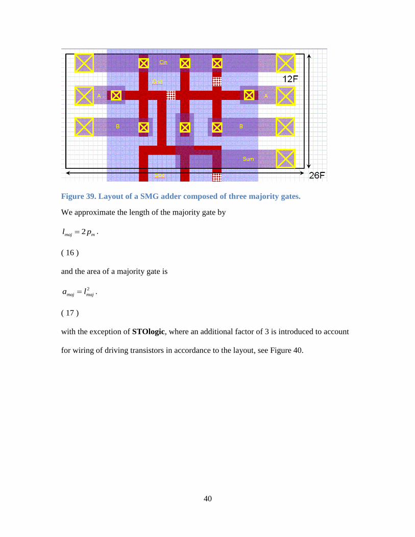
Figure 39. Layout of a SMG adder composed of three majority gates.
We approximate the length of the majority gate by
2maj ml p .
( 16 )
and the area of a majority gate is
2
maj maja l .
( 17 )
with the exception of STOlogic, where an additional factor of 3 is introduced to account
for wiring of driving transistors in accordance to the layout, see Figure 40.

41
Figure 40. Layout of a STOlogic majority gate.
The inverter with fanout of 4 and a NAND gate can be implemented with just one
majority gate
4;inv nand maj gatea a M . ( 18 )
The 1-bit full adder’s area is determined by the number of majority gates required:
1 maj maj bita N a M . ( 19 )
We assume that 3majN majority gates are needed to form a one-bit adder, as it has
been pointed out in [70]. In some cases fewer majority gates are required or they admit a
denser packing. In these cases we adjust the effective number of majority gates to be
2majN for SWD (see Figure 41) and 1majN for NML (see Figure 42).

42
Figure 41. Layout of a SWD one-bit adder.
Figure 42. Layout of a NML one-bit adder.
While ASLD has 2 majority gates per adder due to a clever use of the device’s
functionality, we still set 3majN to correctly account for the cell area (see Figure 43).

43
Figure 43. Layout of ASLD one-bit adder.
Figure 44. Layout of a triangular element of the STT triad.
7.5. Area of STT triad
The area of a triangle element in Figure 45 is estimated to be 17x10F according to the
layout in Figure 44. The area of a NAND gate is estimated the same way too. An inverter
with fanout of four requires four such triangles.

44
4 4inv maj gatea a M . ( 20 )
A 1-bit full adder requires 9 triangles, therefore
1 9 nand bita a M . ( 21 )
Figure 45. Spin transfer torque triad (STTtriad) one-bit adder [29].
The resulting estimates for the areas of beyond-CMOS devices are summarized in Table
6. Note that the intrinsic elements of spintronic logic are larger than those of electronic
logic, but the areas of the adder are smaller. This is due to a richer functionality of the
spintronic majority gates which enables circuits with fewer elements.
F*F Device INVFO4 NAND2 Adder-1b Adder-32b
CMOS HP 36 240 432 5832 279940
CMOS LP 36 240 432 5832 279940
HomJTFET 36 240 576 7776 373250
HETJTFET 36 240 576 7776 373250
gnrTFET 36 240 576 7776 373250
GpnJ 192 288 288 4320 207360
BisFET 24 360 702 9477 454900
SpinFET 36 240 432 5832 279940
STT/DW 20 120 30 630 30240
SMG 64 64 64 288 13824
STTtriad 170 1020 255 3443 165240
STOlogic 128 128 128 576 27648
ASLD 64 64 64 192 9216
SWD 64 64 64 192 9216
NML 64 64 64 96 4608

45
Table 6. Estimate of size of logic circuits, in units of F2.
8. General considerations for switching time and energy
The switching time and energy of the devices strongly depends on the voltage and current
at which they run. The most fruitful avenue for improvement of beyond-CMOS devices
will be to find a lower operating supply voltage [71
] - lower-power alternatives with
resulting large improvement in computing efficiency. In this study we use a relatively
low supply voltage of 10mV for spin torque switching of spintronic devices. The reason
this is possible is that magnetization switching by a current (see Section 11) is unlike
transistor switching. Charging the gate capacitor of a transistor results in raising and
lowering of a potential barrier, which needs to be several times higher than the thermal
energy kT (which corresponds to 26mV) [2] in order to ensure a good turn-off of the
transistor and to suppress standby power dissipation. The potential barrier separating the
logical states is not changed in the magnetization switching, therefore such a
consideration does not limit the supply voltage.
Another factor relevant to both electronic and spintronic circuits is a distribution
of power and ground. In order to minimize active power, the voltage controlling power
needs to be switched on only when a device is being switched. It may be problematic to
switch a power network at a supply voltage smaller than the threshold voltage of a
transistor. By setting this low supply voltage for spintronic devices, we implicitly neglect
the dissipated power in the low voltage power supply source and in the network for the
power and ground distribution. Even though this contribution is significant, a correct
account of it goes beyond the scope of this study. Therefore we provide optimistic

46
estimates for switching delay and energy of the circuits with a voltage of 10mV. For
comparison we provide a more realistic calculation with supply voltage of 100mV.
For voltage-controlled switching of spintronic devices we always use the supply
voltage of 100mV. It is sufficient, considering that the necessary electric field proves to
be small. In this case too, this voltage is not related to raising and lowering the energy
barrier and is not connected to standby power dissipation.
Table 7 contains the input parameter values we use for the benchmark
calculations for each device. Such values need to be obtained from device-level
simulations of the device characteristics. If these inputs change, so might the overall
conclusions from the device comparison. For electronic devices the on-current Ion is taken
for such inputs. For spintronic devices Ion designates the current of the driving transistors,
and we utilize the high-performance CMOS device for this purpose.
Supply voltage Vdd, V Ion, A/m cadjM
CMOS HP 0.73 1805 1
CMOS LP 0.3 2 1
HomJTFET 0.2 25 0.5
HETJTFET 0.4 500 0.5
gnrTFET 0.25 130 0.5
GpnJ 0.7 3125.9 1
BisFET 0.6 900 2
SpinFET 0.7 700 2
for current switching
for voltage switching
STT/DW 0.01 N/A 420 1
SMG 0.01 0.1 1805 1
STTtriad 0.01 0.1 1805 1
STOlogic 0.01 N/A 2344 1
ASLD 0.01 N/A 2344 1
SWD 0.01 0.1 1805 1
NML 0.01 0.1 1805 1
Table 7. Device parameters: supply voltage, on-current, and capacitance adjustment
factor.

47
Since most devices (including spintronic) involve charging and discharging of a capacitor
of some sort, charging/discharging make a major contribution to their performance. We
treat capacitances consistently assuming that the most advanced gate stack is available for
all of the devices. The ideal single gate dielectric capacitance per unit area (F/m2) is
determined via the equivalent oxide thickness
0gac
EOT
. ( 22 )
This capacitance, through the use of EOT, includes both the dielectric capacitance and the
semiconductor (aka quantum) capacitance, while EOT0 would include only the dielectric
capacitance. The ideal single gate capacitance per unit length (F/m) is
gl ga gc c L ( 23 )
The device-dependent adjustment factor cadjM specifies by how much the intrinsic
device gate capacitance is larger (or smaller) than the capacitance of a single gate
dielectric. We take it larger for BisFET and SpinFET due to the capacitance of additional
elements in the device, and we take it smaller for tunneling devices to account for a
smaller gate charge in the on-state, see Table 7. We also include an additional factor of 2
for the BisFET to account for the top and bottom gates. The expression cparM indicates
the value of the parasitic capacitance (gate-to-source, gate-to-drain (Miller), gate-to-
contact, etc.) in terms of the ideal single gate one. We take this factor to be the same for
all devices. The total capacitance (F/m) with the parasitics and the device-dependent
adjustment factor as well as the contact capacitance cC is

48
tl gl cadj cpar cc c M M C ( 24 )
We estimate the capacitance of wires per unit length (F/m) by using the equations [72]
for the capacitance of a line surrounded by two ground planes and two neighboring lines.
2il gr ltolc c c ( 25 )
We take geometrical parameters as described in Table 5. The capacitance (F, farads) of a
typical interconnect between gates is proportional to its length defined in Eq. ( 2 ).
ic il icC c l . ( 26 )
For F=15nm, these capacitances are 126 /ilc aF m and 37.8icC aF .
9. Switching time and energy for electronic devices
The switching time and energy of transistor-like devices (CMOS HP, CMOS LP,
HomJTFET, HETJTFET, gnrTFET, SpinFET, BisFET) are treated in the same
manner. Even though the SpinFET is a spintronic device, the benchmarks considered here
use only static combinational logic circuits, in which the magnetization state of SpinFET
is not reconfigured.
9.1. Intrinsic values for electronic devices
We use extremely simple algebraic equations to estimate their performance. The device
capacitance is
dev tl XC c w . ( 27 )
and the device on-current is
dev on XI I w . ( 28 )
The intrinsic switching time and energy of the device is

49
int /dev dd devt C V I , 2
int dev ddE C V . ( 29 )
We approximate the time and energy of an interconnect as
0.7 /ic ic dd devt C V I , 2
ic ic ddE C V . ( 30 )
We also include an additional factor of 2 in the interconnect delay and energy for the
BisFET to account for more complex interconnects to the device.
9.2. Switching time and energy of GpnJ.
The resistance of the graphene element is composed of the collimation resistance and the
contact resistance
dev coll contR R R . ( 31 )
Graphene resistivity is estimated according to [73]. The collimation resistance
/coll q qR R M , ( 32 )
is determined by the number of quantum modes that can propagate in the graphene sheet
2 /q F gM k w , ( 33 )
which, in turn, is determined by the Fermi momentum set by applied bias V , which
causes electrostatic p- or n-doping of graphene:
FF
F
Ek
v , ( 34 )
where FE is the Fermi energy of carriers in graphene [73].
2
0
0
12F gE eV EOT
EOT
, ( 35 )
where / 2g ddV V and the constant

50
2
0
1
2 F
e
v
. ( 36 )
The contact resistance is inversely proportional to graphene width:
/cont c gR R w . ( 37 )
The on-current per length in the device is
/( )on dd dev gI V R w . ( 38 )
The device capacitance devC which is being switched is that of the middle and side gates
(shown in orange in Figure 37). Their total area is 9F by 3F. To obtain the total
capacitance of the switched MUX one needs to multiply it by tlc . The interconnect
capacitance icC are calculated the same way as for other electronic devices, with
accounting of the area of the graphene device. The quantum capacitance is included in
EOT. The intrinsic device delay and the interconnect delay are
int dev devt C R , ic ic devt C R ( 39 )
The device intrinsic switching energy intE and the interconnect energy icE are calculated
the same way as for other electronic devices.
PARAMETER TYPICAL VALUE
Time factor for inverter, tinvM 0.8
Energy factor for inverter, EinvM 0.8
Time factor for adder, taddM 1.4
Energy factor for adder, EaddM 0.3

51
Parasitic capacitance factor, cparM 1.5
Table 8. Circuit performance parameters.
9.3. Circuit values for electronic devices.
The performance of simple circuits is calculated via the empirical factors in Table 8 that
are chosen to approximately agree with the simulations done with PETE [67]. They
approximately relate to the estimates obtained from comparing the logical efforts of these
gates. For the FO4 inverter, the fanout factor of 4 multiplies the expressions for delay
and energy:
int4inv tinv ict M t t , int4 / 2inv Einv icE M E E . ( 40 )
For the 2-input NAND gate with fanout of 1
intnand tinv ict M t t , int2nand Einv icE M E E , ( 41 )
where the factor of 2 in the expression for the energy corresponds to two transistors in the
pull-up or pull-down networks. For the XOR gate
3xor nant t , xor nanE E . ( 42 )
For the 1-bit full adder
1 2tadd xor nant M t t , 1 2 3Eadd xor nanE M E E . ( 43 )
9.4. Circuit values for GpnJ
GpnJ constitutes a special case. Here an adder contains four MUXes, but the critical
path, from carry-in to carry-out, traverses just one MUX. The energy involves switching
all 10 MUXes

52
1 inttadd ict M t t , 1 int10Eadd icE M E E . ( 44 )
In order to approximately obtain the time and energy benchmarks for the adder, the
benchmarks for one bit are multiplied by the number of bits = 32.
32 132t t , 32 132E E . ( 45 )
10. Common methods of magnetization switching
All spintronic devices considered here contain ferromagnets. In order to switch the
logical state in them, their magnetization needs to be switched. Presently the preferred
way of switching magnetization is with current-controlled switching.
One example, where magnetization switching is done with the magnetic field of current,
is clocking of NML.
Magnetization can also be switched by current via the effect of spin-transfer torque
(STT).
For the case of in-plane magnetization with STT it is assumed that the nanomagnet has
the aspect ratio of 2 and thus the area and volume of
22nm Sa w , nm nm fmv a d . ( 46 )
The energy barrier height [74] is determined via the difference of the element of the
demagnetization tensor in the plane of the nanomagnet yy xxN N N (which are a
function of the ratios of the length, width and thickness and of the shape of a
nanomagnet) as follows

53
2
0 / 2b s nmU N M v . ( 47 )
See parameter definitions in Table 3. We take values approximately corresponding to the
alloy CoFe. The critical current density (after [74]) is
2
0 s fm
c
e M dJ
P
. ( 48 )
We chose to operate with the switching current
3 3dev c c nmI I J a . ( 49 )
Then the switching time is described by [74,75]
2 2log Bs nm
stt
B dev c b
k TeM vt
g P I I U
.
( 50 )
Thus the energy needed to switch is
stt dev dd sttE I V t .
( 51 )
For the case of the perpendicular magnetization STT, it is assumed the aspect ratio is
1, i.e.,
2
nm Sa w , nm nm fmv a d . ( 52 )
The barrier height is determined by the perpendicular magnetic anisotropy (PMA) [76]
b u nmU K v . ( 53 )
We take parameters corresponding to a material with a relatively small saturation
magnetization and high PMA such as CoPtCrB [77]. The critical current density [76] is
2 u fm
c
e K dJ
P
. ( 54 )
The switching time is given by the same expression, Eq. ( 50 ).

54
A more energy efficient, but less technologically mature means of switching of
magnetization is the voltage-controlled switching.
Voltage-controlled switching with an adjacent multiferroic material occurs due to the
effective magnetic field at the interface, that arises through the exchange bias effect. For
this case, we take parameters corresponding to bismuth-ferrite (BiFeO3, BFO) [59,78].
To switch the ferroelectric polarization of the multiferroic material, the capacitance must
be charged from a power supply with a CMOS transistor (we will use the parameters for
CMOS HP here). The switching occurs in a hysteretic manner and is characterized by the
critical field mfE and remanent polarization
mfP . See parameters values in Table 3. The
total charge that needs to be supplied is
2
mf mf S tl X ddQ P w c w V .
(55)
The required thickness of the multiferroic is
ddmf
mf
Vd
E. ( 56 )
The charging energy is
mf mf ddE Q V . ( 57 )
The charging time is
/mf mf devt Q I . ( 58 )
and the magnetization switching time is
2mag
me
tB
.
(59)
The total switching time is the combination of the two.

55
Another way of doing voltage-controlled switching is with an adjacent piezoelectric
material. Changing the polarization in a piezoelectric material causes strain, and the stress
at the interface switches magnetization in the ferromagnet by the magnetostrictive
effect. In an example of switching using a the piezoelectric material such as lead
magnesium niobate-lead titanate (PMN-PT) [60], the switching also has a hysteretic
character. The expressions are similar to Eqs. (55)-(59) with subscript “ms”, except the
polarization is determined via the dielectric constant
0ms ms msP = E . ( 60 )
We also describe here for completeness a similar magnetostrictive switching by the
linear magnetoelectric effect [62]. The strength of coupling is expressed by the
magnetoelectric coefficient (Table 3). However none of the devices in the present study
envision using this type of switching. The electric field in the piezoelectric is
ddme
me
V
dE . ( 61 )
The resulting magnetic field [62] is
me me meB E . ( 62 )
The induced polarization is
0me me meP E . ( 63 )
Another way of switching is by means of a voltage change of surface anisotropy [79]. We
do not cover this method in this paper.
The estimates in this section are used in benchmarking multiple spintronic devices.
Note that we incorporate only the energy contribution of driving transistors, but not
reading circuits (e.g. sense amplifiers). In some cases that latter contribution can become
significant.

56
11. Switching time and energy for spintronic devices
In Section 10 we calculated the switching time and energy for an intrinsic device
switching magnetization. Now we expand it to calculating the performance of spintronic
majority gate circuits. Table 9 specifies which method of controlled switching of
magnetization is assumed, e.g. current-controlled or voltage-controlled, and therefore
which estimates from Section 10 are used for the device’s intrinsic switching time and
energy. For a few of the devices, their method of magnetization switching is specific, and
is described below. As the reader can see, the magnetostrictive rather than multiferroic
option for voltage-controlled switching was selected for the benchmarking since it gives
slightly better projections. For some of the devices we do not envision (indicated with
N/A in Table 9) a voltage-controlled option using the principle of the device operation
relying exclusively on spin transfer torque.
Current-control Voltage-control
STT/DW domain wall STT N/A
SMG perpendicular STT magnetostrictive
STTtriad in-plane STT magnetostrictive
STOlogic perpendicular STT N/A
ASLD perpendicular STT N/A
SWD RF antenna magnetostrictive
NML field of current magnetostrictive
Table 9. Options for current- and voltage controlled switching of spintronic devices.
Here we describe device-specific estimates of the switching time and energy. SMG is
using the intrinsic values from Section 10 directly.
11.1. ASLD intrinsic values
The net electric current flows from the top electrode to the ground and produces the spin
polarization in the interconnect between nanomagnets. This current determines the Joule

57
heating dissipation. The spin polarized electrons diffusion in both directions between two
nanomagnets which causes switching of nanomagnets by spin torque. We introduce an
additional factor of 1.5 to account for the spin-polarized diffusion current being smaller
than the electric current.
11.2. STT-DW intrinsic and circuit values
The magnetization is switched by spin transfer torque of electrons crossing a domain wall
and thus causing its motion. The required current per unit length is (see Table 3 and
Table 4 for material and device parameters)
1.5on dw fmI J d , ( 64 )
where the factor 1.5 is introduced for the excess of the switching current over the critical
one, and this current is passed through the magnetic wire of width F. The speed constant
corresponding to spin torque in domain walls is [80]
/( )stt B dw sv PJ eM . ( 65 )
The speed of domain walls varies and can be approximated by [81]
3dw sttv v . ( 66 )
The intrinsic device (a ferromagnetic wire with domain wall driven through it) switching
time will be the time to move the domain wall past the magnetic tunnel junction (length
2F). The switching energy will be the energy needed to be supplied at the clock such that
the domain wall receives sufficient current to switch.
int 2 / dwt F v , int inton S ddE I w V t . ( 67 )
STT/DW is the only spintronic device envisioned with the NAND (rather than majority
gate) logic functionality. The interconnects there are the usual electrical ones. Their delay
and energy proves to be small compared to intrinsic device values.

58
For the FO4 inverter
intinv ict t t , int4inv icE E E . ( 68 )
For the 2-input NAND gate with fanout of 1
intnand ict t t , intnand icE E E . ( 69 )
For the 1-bit full adder, the critical path goes through two NAND gates and the total
energy is proportional to the area of all the NANDs in the adder:
1 2 nant t , 1 14 nanE E . ( 70 )
11.3. SWD intrinsic values
We assume that the electrical signal exiting the magnetoelectric cell is a harmonic wave
with a frequency 100swf GHz , the corresponding wavelength of spin waves is
30sw nm , the resulting speed of spin waves is
sw sw swv f . ( 71 )
Then the intrinsic switching time is estimated as
int 10/ swt f . ( 72 )
and the interconnect delay is
2 /ic maj swt l v .
( 73 )
11.4. STO logic intrinsic values
The estimates for the device parameters follows the perpendicular STT series of
equations in Section 10, with the exception that we take a typical frequency of
oscillations to be 30oscf GHz , and assume that it has a switching time of

59
int 30/ osct f . ( 74 )
The interconnection between spin torque oscillators is done via spin waves. The
interconnect delay is calculated via the same expression ( 73 ).
In case of voltage-controlled switching, the energy estimates are obtained as in Section
10. In case of the current-controlled switching, the spin wave is excited by a magnetic
field generated by a current in a wire. The estimate of the switching energy is based on
the current required to produce wiB of the magnetic induction at a distance of one pitch of
metal-1
02 /dev wi mI B p . ( 75 )
We use parameters from Table 3 here. The permeability of the substance surrounding the
wire has been demonstrated to have values of 2 to 6, see [82]. Then the dissipated energy
in a transmission line with impedance of 50Z is
2
int intdevE I Zt . ( 76 )
11.5. NML intrinsic values
For NML [83], the switching time of one nanomagnet in the chain forming majority
gates is taken as an empirical value 0.1nmt ns [84,85,86], which presumably does not
change much with the size. The number of nanomagnets (spaced at 2F center to center)
across a majority gate is
/ 2nm majN l F . ( 77 )
We also assume that the interconnect between the majority gates requires one half the
number of nanomagnets as the path through a majority gate. Then the intrinsic switching
time and the interconnect delay are

60
int nm nmt t N . ( 78 )
In case of voltage-controlled switching, the energy estimates are obtained as in Section
10. In case of the current-controlled switching, the magnetic field from a set of electrical
wires is applied to clock the nanomagnets, see Figure 46. We take the wire width to be
mp , the wire pitch to be 2 mp , and the aspect ratio of wires 3AR (corresponding to
tall wires). The required current in a wire is
02 /dev wi mI B p . ( 79 )
Figure 46. Electrical wires for clocking NML [87].
The resistance of the clocking set of wires covering the area is proportional to the area.
Each set of wires is used to clock multiple gates simultaneously. To calculate the power
dissipation of one majority gate, we substitute its area to the expression for resistance
3
maj
clk
m
aR
p AR
. ( 80 )
The energy required to switch over the time of both the device and the interconnect delay
61
2
int intdev coil icE I R t t . ( 81 )
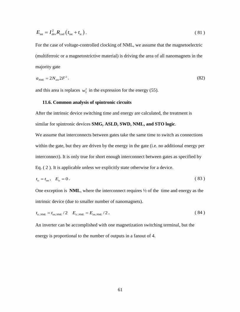
For the case of voltage-controlled clocking of NML, we assume that the magnetoelectric
(multiferroic or a magnetostrictive material) is driving the area of all nanomagnets in the
majority gate
22 2NML nma N F . (82)
and this area is replaces 2
Sw in the expression for the energy (55).
11.6. Common analysis of spintronic circuits
After the intrinsic device switching time and energy are calculated, the treatment is
similar for spintronic devices SMG, ASLD, SWD, NML, and STO logic.
We assume that interconnects between gates take the same time to switch as connections
within the gate, but they are driven by the energy in the gate (i.e. no additional energy per
interconnect). It is only true for short enough interconnect between gates as specified by
Eq. ( 2 ). It is applicable unless we explicitly state otherwise for a device.
intict t , 0icE . ( 83 )
One exception is NML, where the interconnect requires ½ of the time and energy as the
intrinsic device (due to smaller number of nanomagnets).
, int, / 2ic NML NMLt t , int, / 2ic NML NMLE E , ( 84 )
An inverter can be accomplished with one magnetization switching terminal, but the
energy is proportional to the number of outputs in a fanout of 4.

62
intinv ict t t , int4inv icE E E . ( 85 )
A NAND gate is implemented by a majority gate with three inputs. We assume that it
takes the same time to switch as a single input, but the energy is proportional to the
number of inputs
intnand ict t t , int3nand icE E E , ( 86 )
except for NML, where the factor of 3 is absent in the last equation because the energy is
spent on clocking the whole device rather than separate inputs.
A 1-bit full adder performance is given by the number of required majority gates:
1 min(2, )maj nandt N t , 1 maj nand icE N E E . ( 87 )
The contributions of interconnects is accounted in majority gates, except that a full adder
requires an additional interconnect.
11.7. STT triad circuit values
The switching time and energy of STT triad is a special case.
We start with the estimates for the switching time and energy in a triangular in-plane
nanomagnet, Eqs. ( 50 )-( 51 ), of side length 4.5F. The interconnect energy and delay are
calculated like any other electrical interconnect, Section 9. The gate switching time and
energy contain a factor of 2 for the necessity to reset the triangles before switching. In
addition, the switching energy contains a factor of 2 for the two inputs.
int2nand ict t t , int4nand icE E E . ( 88 )
Additionally, a fanout-four inverter requires a triangle per output with the corresponding
factor in the switching energy.

63
int2inv ict t t , int16inv icE E E . ( 89 )
A 1-bit full adder contains totally 9 triangles and 2 output interconnects (for the sum and
the carry) that contribute to the energy. The delay is defined by the critical path through 6
triangles.
1 6 nand ict t t , 1 9 2nand icE E E . ( 90 )
12. Comparison of devices
First we assemble summary of intermediate results - the intrinsic device and interconnect
times and energies for devices (as defined in Sections 9 and 11). The estimates (Table 10)
are performed assuming the use of magnetostrictive switching for spintronic devices
which admit it, and spin torque switching for devices exclusively based on it. Zero
switching energy of interconnects means that either this energy is neglected compared
with the intrinsic device switching energy, or the energy to drive an interconnect is
accounted for in the the intrinsic device switching energy.
device name Delay, int Energy, int Delay, ic Energy, ic
units ps aJ ps aJ
CMOS HP 0.25 19.63 0.18 20.16
CMOS LP 92.08 3.32 66.20 3.40
HomJTFET 3.27 0.98 3.53 1.51
HetJTFET 0.33 3.93 0.35 6.05
gnrTFET 0.79 1.53 0.85 2.36
GpnJ 2.17 142.77 0.28 18.54
BisFET 1.36 22.10 1.18 27.24
SpinFET 1.02 30.08 0.44 18.54
STT/DW 1762.90 111.06 0.02 0.00
STMG 297.61 1.38 297.61 0.00
STTtriad 298.03 10.92 0.02 0.38
STOlogic 1000.00 351.60 80.00 0.00
ASLD 205.16 108.20 205.16 0.00
SWD 297.61 1.38 80.00 0.00

64
NML 400.00 19.31 200.00 9.65
Table 10. Switching delay and switching energy for intrinsic components and
interconnects of devices, for magnetostrictive switching.
Now we summarize the results for all circuits composed of the NRI devices under
consideration. We plot the switching energy vs. switching delay of the three circuits –
fanout-4 inverter, 2-input NAND (see Appendix A), and a 32-bit adder. The plots are
done for various cases ofmagnetization switching.
We point out the extremely important role of voltage-controlled magnetization switching
as opposed to current-controlled switching. With current controlled switching (Figure 47
- Figure 48) spintronics circuits prove to switch significantly slower and require higher
switching energy than electronic circuits. This is related to the limitations of spin torque
switching. The energy could be lowered, if operation with a lower supply voltage, 10mV,
were possible, but then it may face limitations of critical current fluctuations. For a higher
supply voltage, 100mV, the switching energy is correspondingly 10 times higher.

65
Figure 47. Energy vs. delay of 32-bit adders. Spintronic devices use current-
controlled switching with Vdd=0.01V. The preferred corner is bottom left.
Figure 48. Energy vs. delay of 32-bit adders. Spintronic devices use current-
controlled switching with Vdd=0.1V. The preferred corner is bottom left.
10 1
10 2
10 3
10 4
10 5
10 6 10
-1
10 0
10 1
10 2
10 3
10 4
Delay, ps
En
erg
y,
fJ
CMOS HP
CMOS LP
HomJTFET
HetJTFET
gnrTFET
GpnJ
BisFET SpinFET
STT/DW
SMG
STTtriad
STOlogic
ASLD
SWD
NML
32bit adder
10 1
10 2
10 3
10 4
10 5
10 6 10
-1
10 0
10 1
10 2
10 3
10 4
10 5
Delay, ps
En
erg
y,
fJ
CMOS HP
CMOS LP
HomJTFET
HetJTFET
gnrTFET
GpnJ
BisFET
SpinFET
STT/DW SMG
STTtriad
STOlogic
ASLD
SWD
NML
32bit adder

66
With voltage controlled switching (Figure 49 - Figure 50) the intrinsic speed and energy
of spintronic devices can be significantly improved, and spintronic circuits become
competitive with electronic ones. (The exceptions are ASLD, STT/DW and STO logic
which inherently rely on spin torque for operation). Magnetostrictive switching results in
somewhat better switching energy.
Figure 49. Energy vs. delay of 32-bit adders. Spintronic devices use multiferroic
voltage controlled switching. The preferred corner is bottom left.
10 1 10 2 10 3 10 4 10 5 10 6 10 -1
10 0
10 1
10 2
10 3
Delay, ps
En
erg
y,
fJ
CMOS HP
CMOS LP
HomJTFET
HetJTFET
gnrTFET
GpnJ
BisFET
SpinFET
STT/DW
SMG
STTtriad STOlogic
ASLD
SWD
NML
32bit adder
67
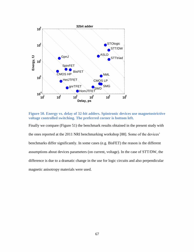
Figure 50. Energy vs. delay of 32-bit adders. Spintronic devices use magnetostrictive
voltage controlled switching. The preferred corner is bottom left.
Finally we compare (Figure 51) the benchmark results obtained in the present study with
the ones reported at the 2011 NRI benchmarking workshop [88]. Some of the devices’
benchmarks differ significantly. In some cases (e.g. BisFET) the reason is the different
assumptions about devices parameters (on current, voltage). In the case of STT/DW, the
difference is due to a dramatic change in the use for logic circuits and also perpendicular
magnetic anisotropy materials were used.
10 1
10 2
10 3
10 4
10 5
10 6 10
-1
10 0
10 1
10 2
10 3
Delay, ps
En
erg
y, fJ
CMOS HP
CMOS LP
HomJTFET
HetJTFET
gnrTFET
GpnJ
BisFET
SpinFET
STT/DW
SMG
STTtriad
STOlogic
ASLD
SWD
NML
32bit adder

68
Figure 51. Energy vs. delay of 2-input NAND gates. Comparison of: NRI
benchmark results [5] (yellow dots) with the present study results using
magnetostrictive voltage controlled switching (blue dots). The preferred corner is
bottom left.
13. Computational throughput and power dissipation
The computational throughput is a measure of useful work performed by a circuit and is
defined as a number of integer operations (32 bit additions in this case) per second per
unit area. We estimate it as
32 32
1addT
a t . ( 91 )
In the process of computation, the expended energy is dissipated as heat power
10 -1
10 0
10 1
10 2
10 3
10 4
10 -4
10 -2
10 0
10 2
Delay, ps
En
erg
y, fJ
CMOS HP
CMOS LP
HomJTFET HetJTFET gnrTFET
GpnJ
BisFET
SpinFET STT/DW
SMG
STTtriad
STOlogic
ASLD
SWD
NML
NAND2
CMOS HP
CMOS LP HomJTFET
HetJTFET
gnrTFET
GpnJ
BisFET
STT/DW
STTtriad
STOlogic
SpinFET ASLD
SWD
NML

69
32diss addP T E . ( 92 )
Since leakage directly measures stand-by power, it is on its own a metric. Those devices
with significant leakage will need power supply gating and this will add to their power. In
this calculation we only account for the active power and for the moment neglect the
stand-by power (e.g. from the leakage currents). The activity factor is determined by the
logic function of the ripple-carry adder and is thus equal to 1/32. We do not introduce
additional activity factors which may be pertinent to specific usage models of circuits.
We also do not incorporate any pipelining in this calculation, even though some logic
technologies are not constrained by power dissipation may produce higher computational
throughput by pipelining. For the sake of simplicity we do not consider the use of multi-
phase clocks.
As we will see from Figure 49 some of the beyond-CMOS devices have
exceptionally low power dissipation and thus are useful for mobile computing.
Benchmark numbers for other devices result in a much higher dissipation. Meanwhile
there is a practical limit to power dissipation set by the ability of a heat sink to remove
power. In this study we (somewhat arbitrarily) set the power density limit (“cap”) to
210 /capP W cm . Note that it is not the whole power dissipated on chip, since we have
not included the contribution of i) long interconnects (longer than bit-to-bit), ii) the clock
distribution circuits and iii) other systems on chip. If the dissipated power exceeds the
limit, one needs to run the circuits slower or spread them apart, thereby decreasing useful
throughput.
Therefore we postulate as a figure merit the computational throughput with a limit on
(capped) power and area (fixed);

70
min(1, / )cap add cap dissT T P P . ( 93 )
The relationship between capped throughput and dissipated power is shown in Figure 52.
The unit of throughput there is peta-integer-operations per second per square centimeter.
We see that only the heterojunction TFET is expected to provide higher throughput than
high-performance CMOS (and do it with lower dissipated power). BisFET and SpinFET
have lower but comparable throughput at the same power. Other tunneling FETs as well
as a few of the spintronics devices provide comparable throughput at significantly lower
power.
We remind the reader that spintronic logic has the major attribute (advantage) of non-
volatility and reconfigurability.
Figure 52. Throughput vs. dissipated power of devices. The preferred corner is
bottom right.
Alternatively these data are also summarized in the following Table 11.
device name Area Delay Energy Power Throughput Thr@<10W/cm2
10 -2
10 -1
10 0
10 1 10
-2
10 -1
10 0
10 1
10 2
Throughput, PIOPS/cm 2
Po
we
r, W
/cm
2
CMOS HP
CMOS LP
HomJTFET
HetJTFET
gnrTFET
GpnJ BisFET
SpinFET
STT/DW
SMG STTtriad
STOlogic ASLD
SWD NML
32bit adder

71
units m2 ps fJ W/ cm2 Pops/s/ cm2 Pops/s/ cm2
CMOS HP 63.0 84 2.48 46.5 18.79 4.04
CMOS LP 63.0 31331 0.42 0.0 0.05 0.05
HomJTFET 84.0 1378 0.15 0.1 0.86 0.86
HetJTFET 84.0 138 0.59 5.1 8.64 8.64
gnrTFET 84.0 331 0.23 0.8 3.60 3.60
GpnJ 46.7 110 15.49 301.5 19.47 0.65
BisFET 102.4 508 3.00 5.8 1.92 1.92
SpinFET 63.0 282 3.20 18.0 5.63 3.13
STT/DW 6.8 112820 50 6.5 0.13 0.13
STMG 3.1 38094 0.40 0.3 0.84 0.84
STTtriad 37.2 114450 13.04 0.3 0.02 0.02
STOlogic 6.2 69120 101 23.5 0.23 0.10
ASLD 2.1 26261 20.78 38.2 1.84 0.48
SWD 2.1 12084 0.26 1.1 3.99 3.99
NML 1.0 38400 1.24 3.1 2.51 2.51
Table 11. Summary of comparison of devices for magnetostrictive voltage controlled
switching.
14. Discussion of benchmarks
We observe that two major conclusions are derived from this study.
1) For electronic devices, the most promising avenue of improvement is decreasing
the operational voltage. Tunneling FETs seem to be the leading option.
2) Spintronic devices have an advantage in implementing complex logic functions
with a smaller number of devices/elements. The key factor toward making them
competitive with CMOS is using voltage controlled switching.
We would like to stress two additional advantages of spintronic devices that are not
captured by the current set of benchmarks – non-volatility and reconfigurability. In order
to utilize these advantages new types of circuits need to be designed.

72
To make the task tractable, we considered only a small set of circuits. In order to cover
all elements necessary for an arithmetic logic unit (ALU), one needs to extend this
treatment to state elements, latches, multiplexors/demultiplexors, etc.
15. Conclusions
An approach with simple but general estimates of benchmark parameters has been
described that is applicable to multiple devices and provides a consistent and
reproducible methodology that can be used in the benchmarking of NRI devices. By
publishing this paper the authors solicit inputs and suggestions from the researchers in the
field in order to find uniform consensus on the way to do benchmarking for beyond-
CMOS devices.
16. Acknowledgements
The authors would like to thank George Bourianoff, Brian Doyle, Charles Kuo, Uygar
Avci, Raseong Kim, and Sasikanth Manipatruni for fruitful discussions on beyond-
CMOS devices; Arijit Raychowdhury and Charles Augustine for help with the PETE
simulator; Kerry Bernstein and Jeff Welser for helpful comments. We are immensely
grateful to researchers in Nanoelectronics Research Initiative – Jim Allen, Marc Baldo,
Behtash Behin-Aein, Gyorgy Csaba, Jean Anne Currivan, Suman Datta, Supriyo Datta,
Kos Galatsis, Yunfei Gao, Sharon Hu, Alexander Khitun, Alexander Kozhanov, Ilya
Krivorotov, Ji Ung Lee, Mark Lundstrom, Allan MacDonald, Dejan Markovic, Azad
Naeemi, Vijay Narayanan, Michael Niemier, Chenyun Pan, Wolfgang Porod, Kaushik
Roy, L. Frank Register, Caroline Ross, Sayeef Salahuddin, Vinay Saripalli, Angik Sarkar,

73
Alan Seabaugh, Srikant Srinivasan – for providing us a wealth details of their approach to
benchmarking beyond-CMOS devices and spending significant time and effort in helping
us understand their operation.
17. Appendix A.
This section contains the comparison plots for devices in addition to ones in the main
text. These provide more perspective on the relative differences amongst the devices.
Figure 53. Energy vs. delay of inverters with fanout of 4. Spintronic devices use
current-controlled switching with Vdd=0.01V. The preferred corner is bottom left.
10 -1
10 0
10 1
10 2
10 3
10 4 10
-3
10 -2
10 -1
10 0
10 1
10 2
Delay, ps
En
erg
y,
fJ
CMOS HP
CMOS LP
HomJTFET
HetJTFET
gnrTFET
GpnJ
BisFET
SpinFET STT/DW
SMG
STTtriad
STOlogic
ASLD
SWD NML
INVFO4

74
Figure 54. Energy vs. delay of 2-input NAND gates. Spintronic devices use current-
controlled switching with Vdd=0.01V. The preferred corner is bottom left.
Figure 55. Energy vs. delay of inverters with fanout of 4. Spintronic devices use
current-controlled switching with Vdd=0.1V. The preferred corner is bottom left.
10 -1
10 0
10 1
10 2
10 3
10 4 10
-3
10 -2
10 -1
10 0
10 1
10 2
Delay, ps
En
erg
y,
fJ
CMOS HP
CMOS LP
HomJTFET
HetJTFET
gnrTFET
GpnJ
BisFET
SpinFET STT/DW SMG
STTtriad
STOlogic
ASLD
SWD
NML
NAND2
10 -1
10 0
10 1
10 2
10 3
10 4 10
-3
10 -2
10 -1
10 0
10 1
10 2
10 3
Delay, ps
En
erg
y,
fJ
CMOS HP
CMOS LP
HomJTFET
HetJTFET
gnrTFET
GpnJ
BisFET
SpinFET
STT/DW SMG
STTtriad
STOlogic
ASLD
SWD
NML
INVFO4
75
Figure 56. Energy vs. delay of 2-input NAND gates. Spintronic devices use current-
controlled switching with Vdd=0.1V. The preferred corner is bottom left.
Figure 57. Energy vs. delay of inverters with fanout of 4. Spintronic devices use
multiferroic voltage controlled switching. The preferred corner is bottom left.
10 -1
10 0
10 1
10 2
10 3
10 4 10
-3
10 -2
10 -1
10 0
10 1
10 2
10 3
Delay, ps
En
erg
y,
fJ
CMOS HP
CMOS LP
HomJTFET
HetJTFET
gnrTFET
GpnJ
BisFET
SpinFET
STT/DW SMG
STTtriad
STOlogic
ASLD
SWD
NML
NAND2
10 -1 10 0 10 1 10 2 10 3 10 4 10 -3
10 -2
10 -1
10 0
10 1
Delay, ps
En
erg
y,
fJ
CMOS HP
CMOS LP HomJTFET
HetJTFET
gnrTFET
GpnJ
BisFET
SpinFET
STT/DW
SMG
STTtriad STOlogic
ASLD
SWD
NML
INVFO4

76
Figure 58. Energy vs. delay of 2-input NAND gates. Spintronic devices use
multiferroic voltage controlled switching. The preferred corner is bottom left.
Figure 59. Energy vs. delay of inverters with fanout of 4. Spintronic devices use
magnetostrictive voltage controlled switching. The preferred corner is bottom left.
10 -1 10 0 10 1 10 2 10 3 10 4 10 -3
10 -2
10 -1
10 0
10 1
Delay, ps
En
erg
y,
fJ
CMOS HP
CMOS LP
HomJTFET
HetJTFET
gnrTFET
GpnJ
BisFET
SpinFET STT/DW
SMG
STTtriad
STOlogic
ASLD
SWD
NML
NAND2
10 -1
10 0
10 1
10 2
10 3
10 4 10
-3
10 -2
10 -1
10 0
10 1
Delay, ps
En
erg
y, fJ
CMOS HP
CMOS LP
HomJTFET
HetJTFET
gnrTFET
GpnJ
BisFET
SpinFET
STT/DW
SMG
STTtriad
STOlogic
ASLD
SWD
NML
INVFO4

77
Figure 60. Energy vs. delay of 2-input NAND gates. Spintronic devices use
magnetostrictive voltage controlled switching. The preferred corner is bottom left.
Figure 61. Ratio of the delay of the 32-bit adders and their intrinsic device delay vs.
intrinsic device.
10 -1
10 0
10 1
10 2
10 3
10 4 10
-3
10 -2
10 -1
10 0
10 1
Delay, ps
En
erg
y, fJ
CMOS HP
CMOS LP
HomJTFET
HetJTFET
gnrTFET
GpnJ
BisFET
SpinFET STT/DW
SMG
STTtriad
STOlogic
ASLD
SWD
NML
NAND2

78
Figure 62. . Ratio of switching energy of the 32-bit adders and their intrinsic device
switching energy vs. intrinsic device switching energy.
Figure 63. Ratio of the energy-delay product of the 32-bit adders and their intrinsic
device energy-delay product vs. intrinsic device energy-delay product .

79
Figure 64. Charge vs. voltage for intrinsic devices.
Figure 65. Current vs. voltage for intrinsic devices.

80
Figure 66. Capacitance vs. resistance of intrinsic devices.
Figure 67. Charge vs. resistance of intrinsic devices.

81
18. References
1 International Technology Roadmap for Semiconductors, available http://www.itrs.net/,
Chapter PIDS (2011).
2 V. V. Zhirnov, R. K. Cavin, J. A. Hutchby, and G. I. Bourianoff, “Limits
to binary logic switch scaling - a gedanken model,” Proceeding IEEE, vol. 91,
no. 11, pp. 1934–1939, Nov. 2003.
3 K. Bernstein, presentation, NRI Benchmarking Workshop, Aug. 2010. Also see K.
Bernstein, R. K. Cavin III, W. Porod, A. Seabaugh, and J. Welser, “Device and
Architecture Outlook for Beyond-CMOS Switches”, Proceedings IEEE v. 98, pp. 2169-
84 (2010).
4 Available online: https://nanohub.org/tools/nribench/browser/trunk/src.
5 K. Bernstein, presentation, NRI Annual Review. Nov. 2011.
6 C. Reischer and D. A. Simovici, “On the implementation of set-valued non-Boolean
switching functions”, Proceedings of the 21st International Symposium on Multiple-
Valued Logic, pp. 166-172 (1991).
7 C. Mead, “Neuromorphic electronic systems”, Proceedings of the IEEE, v. 78, pp. 1629
– 1636 (1990).
8 “Nanoelectronics and Information Technology”, ed. R. Waser (Wiley-VCH, Berlin,
2005).
9 I. Zutic, J. Fabian, and S. Das Sarma, “Spintronics: Fundamentals and applications”,
Rev. Mod. Phys. 76, 323 (2004).

82
10 D. E. Nikonov and G. I. Bourianoff, “Operation and Modeling of Semiconductor
Spintronics Computing Devices”, J. Supercond. and Novel Magnetism, v. 21, no. 8, pp.
479-493 (2008).
11 U. E. Avci, R. Rios, K. Kuhn, I. A. Young, “Comparison of performance, switching
energy and process variations for the TFET and MOSFET in logic”, Proceedings of the
2011 VLSI Technology Symposium, pp. 124-125, June 2011.
12 A. C. Seabaugh and Q. Zhang, “Low-Voltage Tunnel Transistors for Beyond-CMOS
Logic”, Proceedings IEEE, v. 98, pp. 2095-2010 (2010).
13 H. Kroemer, “A proposed class of hetero-junction injection lasers”, Proceedings of the
IEEE, v. 51, pp. 1782 – 1783 (1963).
14 M. Luisier and G. Klimeck, “Performance analysis of statistical samples of graphene
nanoribbon tunneling transistors with line edge roughness”, Appl. Phys. Lett. v. 94,
223505 (2009).
15 S. O. Koswatta, M. S. Lundstrom, and D. E. Nikonov, “Performance Comparison
Between p-i-n Tunneling Transistors and Conventional MOSFETs”, IEEE Transactions
on Electronic Devices v. 56, pp. 456-465 (2009).
16 T. Low and J. Appenzeller, “Electronic transport properties of a tilted graphene p-n
junction”, Phys. Rev. B v.80, 155406 (2009).
17 D. Reddy, L. F. Register, E. Tutuc, and Sanjay K. Banerjee, “Bilayer PseudoSpin
Field-Effect Transistor (BiSFET): A Proposed New Logic Device”, IEEE Trans.
Electronic Devices, v. 30, pp. 158 – 160 (2009).
18 H. Min, R. Bistritzer, J.-J. Su, and A. H. MacDonald, “Room-temperature

83
superfluidity in graphene bilayers,” Phys. Rev. B, Condens. Matter,
vol. 78, no. 12, p. 121401 (2008).
19 M. Y. Kharitonov and K. B. Efetov, “Excitonic condensation in a double-layer
graphene system” Semicond. Sci. Technol. v. 25, p. 034004 (2010).
20 M. J. Gilbert, “Performance Characteristics of Scaled Bilayer
Graphene Pseudospin Devices”, IEEE T. Electron Devices, v. 75, pp. 3059-67 (2010).
21 B. Dellabetta and M. J. Gilbert, “Performance characteristics of strongly correlated
bilayer graphene for post-CMOS logic devices”, Silicon Nanoelectronics Workshop
(SNW), pp. 1-2 (2010).
22 B. Dellabetta and M. J. Gilbert, Device Research Conference (DRC) digest, “Effect of
disorder on superfluidity in double layer graphene”, pp. 65 – 66 (2011).
23 L. F. Register, X. Mou, D. Reddy, W. Jung, I. Sodeman, D. Pesin, A. Hassibi, A. H.
MacDonald, and S. K. Banerjee, “Bilayer Pseudo-Spin Field Effect Transistor (BiSFET):
Concepts and Critical Issues for Realization”, ECS Transactions (2012).
24 S. Sugahara and M. Tanaka, "A spin metal–oxide–semiconductor field-effect transistor
using half-metallic-ferromagnet contacts for the source and drain," Applied Physics
Letters, vol. 84, p. 2307 (2004).
25 K. Galatsis, presentation, NRI Benchmarking Workshop, Aug. 2011.
26 J. A. Currivan, Y. Jang, M. D. Mascaro, M. A. Baldo, and C. A. Ross, “Low Energy
Magnetic Domain Wall Logic in Short, Narrow Ferromagnetic Wires”, IEEE Mag. Lett.
(2012), to be published.

84
27 D. E. Nikonov and G. I. Bourianoff, “Recent progress, opportunities and challenges for
beyond-CMOS information processing technologies”, ECS Trans., v. 35, no. 2, pp. 43–
53, May 2011.
28 D. E. Nikonov, G.I. Bourianoff, and T. Ghani, “Proposal of a Spin Torque Majority
Gate Logic”, IEEE Electron. Device Lett., v. 32, n. 8, pp. 1128-30, Aug. 2011.
29 A. Kozhanov and J. Allen, presentation, NRI Benchmarking Workshop, Aug. 2011.
30 I. Krivorotov and D. Markovic, presentation, NRI Benchmarking Workshop, Aug.
2011.
31 B. Behin-Aein, D. Datta, S. Salahuddin, and S. Datta, “Proposal for an all-spin logic
device with built-in memory”, Nature Nano v. 5, p. 266 (2010).
32 B. Behin-Aein, A. Sarkar, S. Srinivasan and S. Datta, "Switching energy-delay of all
spin logic devices", Appl. Phys. Lett. 98, 123510, 2011.
33 C. Augustine, G. Panagopoulos, B. Behin-Aein, S. Srinivasan, A. Sarkar, and K. Roy,
“Low-Power Functionality Enhanced Computation Architecture Using Spin-Based
Devices”, IEEE International Symposium on Nanoscale Architectures (NANOARCH), p.
129-136 (2011).
34 A. Khitun and K. L. Wang, “Nano scale computational architectures with Spin Wave
Bus”, Superlatt. and Microstruct. 38, 184 (2005).
35 A. Khitun, M. Bao, J.-Y. Lee, K. L. Wang, D. W. Lee, S. X. Wang, and I. V. Roshchin,
“Inductively Coupled Circuits with Spin Wave Bus for Information Processing”, J. of
Nanoelectronics and Optoelectronics 3, 24 (2008).

85
36 R. P. Cowburn and M. E. Welland, “Room Temperature Magnetic Quantum Cellular
Automata”, Science 287, 1466 (2000).
37 S. Datta and B. Das, "Electronic analog of the electro optic modulator," Applied
Physics Letters, vol. 56, pp. 665-667 (1990).
38 M. Kabir, D. Unluer, L. Li, A. W. Ghosh, M. R. Stan, “Electronic ratchet: A non-
equilibrium, low power switch”, 11th
IEEE Conference on Nanotechnology, pp. 482-486
(2011).
39 Y. P. Chen and J. Hu, presentation, NRI Benchmarking Workshop, Aug. 2010.
40 V. Saripalli, V. Narayanan, and S. Datta, “Ultra Low Energy Binary Decision Diagram
Circuits Using Few Electron Transistors”, Nano-Net, Lecture Notes of the Institute for
Computer Sciences, Social Informatics and Telecommunications Engineering, v. 20, Part
2, pp. 200-209, Springer, 2009.
41 H. Raza, E. C. Kan, T. Z. Raza, T.-H. Hou, “On the Possibility of an Electronic-
structure Modulation Transistor”, online http://arxiv.org/abs/0812.0123v2 (2009).
42 S. A. Wolf, J. Lu, M. R. Stan, E. Chen, and D. M. Treger, “The Promise of
Nanomagnetics and Spintronics for Future Logic and Universal Memory”, Proceedings
IEEE, v. 98, pp. 2155-2168 (2010).
43 M. Kabir, M. R. Stan, S. A. Wolf, R. B. Comes, J. Lu, “RAMA: a self-assembled
multiferroic magnetic QCA for low power systems”, Proceedings of the 21st edition of
the Great lakes symposium on VLSI, pp. 25-30, 2011.
44 H. Chen, L. F. Register, S. K. Banerjee, “Resonant Injection Enhanced Field Effect
Transistor for Low Voltage Switching: Concept and Quantum Transport Simulation”,

86
International Conference on Simulation of Semiconductor Processes and Devices
(SISPAD '09), pp.1-4, 2009.
45 D. A. Allwood, G. Xiong, C. C. Faulkner, D. Atkinson, D. Petit, and R. P. Cowburn,
“Magnetic domain-wall logic”, Science 309, 1688 (2005).
46 D. E. Nikonov, G. I. Bourianoff, and P. A. Gargini, “Simulation of Highly Idealized,
Atomic Scale Magnetic Quantum Cellular Automata Logic Circuits”, Journal of
Nanoelectronics and Optoelectronics 3, 3 (2008).
47 D. M. Newns, J. A. Misewich, C. C. Tsuei, A Gupta, B. A. Scott, and A. Schrott, “Mott
transition field effect transistor”, Appl. Phys. Lett. 73, 780 (1998).
48 J. Wunderlich,B.-G. Park, A. C. Irvine, L. P. Zârbo, E. Rozkotová, P. Nemec, V.
Novák, J. Sinova, T. Jungwirth, “Spin Hall Effect Transistor”, Science v. 330, pp. 1801-
1804 (2010).
49 P. M. Koenraad and M. E. Flatté, “Single dopants in semiconductors”, Nature
Materials, v. 10, pp. 91–100 (2011).
50 A. Ney, C. Pampuch, R. Koch & K. H. Ploog, “Programmable computing with a single
magnetoresistive element”, Nature 425, 485 (2003).
51 J. Wang, H. Meng, and J.-P. Wang, “Programmable spintronics logic device based on a
magnetic tunnel junction element”, J. Appl. Phys. 97, 10D509 (2005).
52 S. Lee, S. Choa, S. Lee, and H. Shin, “Magneto-Logic Device Based on a Single-Layer
Magnetic Tunnel Junction”, IEEE Trans. Electron. Devices 54, 2040 (2007).

87
53 S. Matsunaga, J. Hayakawa, S. Ikeda, K. Miura, H. Hasegawa, T. Endoh, H. Ohno, and
T. Hanyu, “Fabrication of a Nonvolatile Full Adder Based on Logic-in-Memory
Architecture Using Magnetic Tunnel Junctions”, Appl. Phys. Express 1, 091301 (2008).
54 A.A. High, A.T. Hammack, L.V. Butov, M. Hanson, A.C. Gossard, “Exciton
optoelectronic transistor”, Optics Letters 32, 2466 (2007).
55 A.A. High, E.E. Novitskaya, L.V. Butov, M. Hanson, A.C. Gossard, “Control of
exciton fluxes in excitonic integrated circuits”, Science 321, 229 (2008).
56 G. Grosso, J. Graves, A.T. Hammack, A.A. High, L.V. Butov, M. Hanson, A.C.
Gossard, “Excitonic switches operating at around 100 K”, Nature Photonics 3, 577
(2009).
57 International Technology Roadmap for Semiconductors, available http://www.itrs.net/,
Chapter ERD (2011).
58 J. U. Lee, “Single Exciton Quantum Logic Circuits”, IEEE J. Quant. Electronics, v. 48,
pp. 1158-64 (2012).
59 J. Wang, J. B. Neaton, H. Zheng, V. Nagarajan, S. B. Ogale, B. Liu, D. Viehland, V.
Vaithyanathan, D. G. Schlom, U. V. Waghmare, N. A. Spaldin, K. M. Rabe, M. Wuttig,
and R. Ramesh, “Epitaxial BiFeO3 Multiferroic Thin Film Heterostructures”, Science, v.
299, pp. 1719-1722, March 2003.
60 P. Shabadi, A. Khitun, K. Wong, P. K. Amiri, K. L. Wang, and C. A. Moritz, “Spin
wave functions nanofabric update”, Proc. IEEE/ACM Intl. Symposium on Nanoscale
Architectures, pp. 107-113 (2011).

88
61 T. Wu, A. Bur, P. Zhao, K. P. Mohanchandra, K. Wong, K. L. Wang, C. S. Lynch, and
G. P. Carman, “Giant electric-field-induced reversible and permanent magnetization
reorientation on magnetoelectric Ni/011[Pb(Mg1/3Nb2/3)O(1−x)–PbTiO3x
heterostructure”, Appl. Phys. Lett. 98, 012504 (2011).
62 M. Fiebig, “Revival of the magnetoelectric effect“, J. Phys. D: Appl. Phys. 38, R123–
R152 (2005).
63 J. A. Rabaey “Design Rules”, available
http://bwrc.eecs.berkeley.edu/classes/icbook/SLIDES/design_rules.ppt. Also see
http://www.mosis.com/files/scmos/scmos.pdf.
64 N. Weste and D. Harris, “CMOS VLSI Design: A Circuits and Systems Perspective”,
4th ed. (Addison Wesley, 2010).
65 C. Auth et al., “A 22nm High Performance and Low-Power CMOS Technology
Featuring Fully-Depleted Tri-Gate Transistors, Self-Aligned Contacts and High Density
MIM Capacitors”, Symposium on VLSI Technology Digest of Technical Papers, pp. 131-
132 (2012) .
66 H. Liu, D. K. Mohata, A. Nidhi, V. Saripalli, V. Narayanan and S. Datta, “Exploration
of Vertical MOSFET and Tunnel FET Device Architecture for Sub 10nm Node
Applications”, Device Research Conference Digest, p. 233-234 (2012).
67 C. Augustine, A. Raychowdhury, Y. Gao, M. Lundstrom, and K. Roy, “PETE: A
device/circuit analysis framework for evaluation and comparison of charge based
emerging devices”, International Symposium on Quality of Electronic Design, p. 80-85
(2009).

89
68 L. F. Register, D. Basu, and D. Reddy, “From Coherent States in Adjacent Graphene
Layers toward Low-Power Logic Circuits”, Advances in Condensed Matter Physics, v.
2011, 258731 (2011).
69 C. Pan and A. Naeemi, private communication.
70 G. L. Snider, A. O. Orlov, I. Amlani, X. Zuo, G. H. Bernstein, C. S. Lent, J. L. Merz,
and W. Porod, “Quantum-dot cellular automata: Review and recent experiments
(invited)”, J. Appl. Phys. 85, 4283 (1999).
71 Y. Gao, T. Low, and M. Lundstrom, “Possibilities for VDD = 0.1V Logic Using
Carbon-Based Tunneling Field Effect Transistors”, Symposium on VLSI Technology
Digest of Technical Papers, pp. 180-181 (2009).
72 J. A. Davis, V. K. De, and J. D. Meindl, “A Stochastic Wire-Length Distribution for
Gigascale Integration (GSI)—Part II: Applications to Clock Frequency, Power
Dissipation, and Chip Size Estimation”, IEEE Trans. Electron Devices, v. 45, pp. 590-
597 (1998).
73 S. Tanachutiwat, J. U. Lee, and W. Wang, “Reconfigurable Multi-Function Logic
Based on Graphene P-N Junctions”, Proceedings of Design Automation Conference, pp.
883-888, Anaheim, California, USA, June 13-18, 2010.
74 J. Z. Sun, “Spin angular momentum transfer in current-perpendicular nanomagnetic
junctions”, IBM J. Res. Dev. 50, 81-100 (2006).
75 R. H. Koch, J. A. Katine, and J. Z. Sun, “Time-Resolved Reversal of Spin-Transfer
Switching in a Nanomagnet”, Phys. Rev. Lett., v. 92, 088302 (2004).

90
76 S. Mangin, D. Ravelsona, J. A. Katine, M. J. Carey, B. D. Terris, and E. Fullerton,
“Current-induced magnetization reversal in nanopillars with perpendicular anisotropy”,
nature Materials, 5, 210-215 (2006).
77 M. F. Toney, E. E. Marinero, M. F. Doerner, and P. M. Rice, “High anisotropy
CoPtCrB magnetic recording media”, J. Appl. Phys. v. 94, pp. 4018-4023 (2003).
78 J. T. Heron, M. Trassin, K. Ashraf, M. Gajek, Q. He, S.Y. Yang, D. E. Nikonov, Y-H.
Chu, S. Salahuddin, and R. Ramesh, “Electric-Field-Induced Magnetization Reversal in a
Ferromagnet-Multiferroic Heterostructure”, Phys. Rev. Lett. 107, 217202 (2011).
79 T. Maruyama, Y. Shiota, T. Nozaki, K. Ohta, N. Toda, M. Mizuguchi, A. A.
Tulapurkar, and T. Shinjo, M. Shiraishi, S. Mizukami, Y. Ando and Y. Suzuki, “Large
voltage-induced magnetic anisotropy change in a few atomic layers of iron”, Nature
Nano. 4, pp. 158-161 (2009).
80 A. V. Khvalkovskiy, K. A. Zvezdin, Y. V. Gorbunov, V. Cros, J. Grollier, A. Fert, and
A. K. Zvezdin, “High domain wall velocities due to spin currents perpendicular to the
plane,” Phys. Rev. Lett., vol. 102, no. 6, p. 067 206, Feb. 2009.
81 C. A. Ross, INDEX review presentation, 2010.
82 S. V. Pietambaram, N. D. Rizzo, R. W. Dave, J. Goggin, K. Smith, J. M. Slaughter,
and S. Tehrani, “Low-power switching in magnetoresistive random access memory bits
using enhanced permeability dielectric films ”, Appl. Phys. Lett. 90, 143510 (2007).
83 A. Imre, G. Csaba, L. Ji, A. Orlov, G. H. Bernstein, W. Porod, "Majority logic gate for
magnetic quantum-dot cellular automata," Science, v. 311, pp. 205-208, (2006).

91
84 Th. Gerrits, H. A. M. van den Berg, J. Hohlfeld, L. Bar, Th. Rasing, Nature 418, 509
(2002).
85 D. B. Carlton, N. C. Emley, E. Tuchfeld, and J. Bokor, “Simulation Studies of
Nanomagnet-Based Logic Architecture”, Nano Lett., v. 8 , pp. 4173–4178 (2008).
86 F. M. Spedalieri, A. P. Jacob, D. E. Nikonov, V. P. Roychowdhury, “Performance of
Magnetic Quantum Cellular Automata and Limitations Due to Thermal Noise”, IEEE
Trans. Nano., v.10, n. 5, pp. 537-546 (2011).
87 M. Niemier, private communication.
88 K. Bernstein, presentation, NRI Benchmarking Workshop, Aug. 2011.