
UNIT I Power Supplies Biasing BJT and MOSFET Outline Rectifier BJT Biasing FET Biasing.

Operation Modes of BJT and MOSFETCutoff, Active and Saturation
Ang Man ShunDecember 13, 2012
ReferenceSedra and Smith Microelectronic CircuitNeamen Microelectronics
1 BJT1.1 Cutoff Mode
• When VI < VBE(on), it can not turn on the BE-Junction diode, the BJT is in cutoff mode
1.2 Forward Active Mode• When VI > VBE(on) , IB ̸= 0 and VCE > 0.2V
1
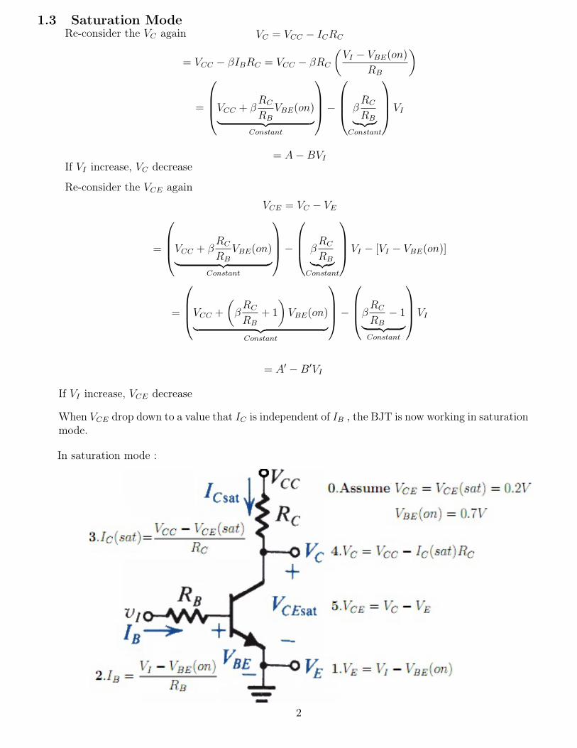
1.3 Saturation ModeRe-consider the VC again VC = VCC − ICRC
= VCC − βIBRC = VCC − βRC
(VI − VBE(on)
RB
)
=
VCC + βRC
RB
VBE(on)︸ ︷︷ ︸Constant
−
βRC
RB︸ ︷︷ ︸Constant
VI
= A−BVI
If VI increase, VC decrease
Re-consider the VCE again
VCE = VC − VE
=
VCC + βRC
RB
VBE(on)︸ ︷︷ ︸Constant
−
βRC
RB︸ ︷︷ ︸Constant
VI − [VI − VBE(on)]
=
VCC +
(βRC
RB
+ 1
)VBE(on)︸ ︷︷ ︸
Constant
−
βRC
RB
− 1︸ ︷︷ ︸Constant
VI
2
= A′ −B′VI
If VI increase, VCE decrease
When VCE drop down to a value that IC is independent of IB , the BJT is now working in saturationmode.
In saturation mode :

VCE in this case will be smaller than VCE(sat) = 0.2V :
VCE = VC − VE
= (VCC − IC(sat)RC)− (VI − VBE(on))
= (VCC + VBE(on))− VI − IC(sat)RC
VCE = (VCC + VBE(on))− VI −VCC − VCE(sat)
RC
RC
VCE = VCE(sat)−
VI − VBE(on)︸ ︷︷ ︸>0
VI > VBE(on) , otherwise, cutoff mode ( contradiction ! ), thus VI − VBE(on) > 0 , and thus
VCE = VCE(sat)−
VI − VBE(on)︸ ︷︷ ︸>0
< VCE(sat)
VCE < VCE(sat) ≈ 0.2V
3
2 MOSFET

Cosider the MOS capacitor QCap = CVcap
The VCap is the excess voltage of VGS : VCap = VGS − VTN
QCap = C (VGS − VTN)
Jd = C (VGS − VTN)µnVDS
L
I = JdW = CµnW
L(VGS − VTN)VDS = kn
W
L(VGS − VTN)VDS ( In the S-side)
I = JdW = CµnW
L(VGS − VTN)VDS = kn
W
L(VGS − VTN − VDS)VDS (In the D-side)
In the middle of the device, assume linear relationship, the average current
IDS =knW
L
(VGS − VTN − VDS
2
)VDS
2.1.3 Saturation
When VDS = VGS − VTN
IDS = knW
L
(VGS − VTN − VGS − VTN
2
)(VGS − VTN) =
kn2
W
L(VGS − VTN)
2 = Kn (VGS − VTN)2
4
2.1 MOSFET Device
2.1.1 Cutoff
When VGS = 0, the MOSFET is just like two back-to-back diode, no current, so cut off.IDS = 0When VGS > 0 but VGS < VTN , since the MOSFET structure looks like a capacitor, there is somepositive charge stored in the metal plate, while in the semiconductor, there is some negative charge.Since the VGS is not large enough , so there is no “n−channel” , there is still no current.
2.1.2 Triode / Active
When VGS > VTN , there is enough voltage or E-field attraction to establish a n−channel in thesemiconductor, so the 2 n-semiconductor can now have current pass through. IDS ̸= 0
• The E-field that cause the current to drift : EDS =VDS
L
• Thus the drift velocity is vd = µnEDS = µnVDS
L
• Thus the drift current density (in A/m) is Jd = Qvd = QCapµnVDS
L
• Where the Q ( in C/m ) is the charge that drift in the n-channel, it comes from the charges storedin MOS capacitor QCap

−END−5
2.2.3 Triode / Active
2.2.2 Saturation
2.2 MOSFET Circuit Operation
2.2.1 Cutoff