
CHAPTER 3 Frequency Response of Basic BJT and …rabinr/Web_ELEC_312/Past year... · CHAPTER 3...
42
CHAPTER 3 Frequency Response of Basic BJT and MOSFET Amplifiers (Review materials in Appendices III and V) In this chapter you will learn about the general form of the frequency domain transfer function of an amplifier. You will learn to analyze the amplifier equivalent circuit and determine the critical frequencies that limit the response at low and high frequencies. You will learn some special techniques to determine these frequencies. BJT and MOSFET amplifiers will be considered. You will also learn the concepts that are pursued to design a wide band width amplifier. Following topics will be considered. Review of Bode plot technique. Ways to write the transfer (i.e., gain) functions to show frequency dependence. Band-width limiting at low frequencies (i.e., DC to f L ). Determination of lower band cut- off frequency for a single-stage amplifier – short circuit time constant technique. Band-width limiting at high frequencies for a single-stage amplifier. Determination of upper band cut-off frequency- several alternative techniques. Frequency response of a single device (BJT, MOSFET). Concepts related to wide-band amplifier design – BJT and MOSFET examples. 3.1 A short review on Bode plot technique Example: Produce the Bode plots for the magnitude and phase of the transfer function 2 5 10 () (1 /10 )(1 /10 ) s Ts s s , for frequencies between 1 rad/sec to 10 6 rad/sec. We first observe that the function has zeros and poles in the numerical sequence 0 (zero), 10 2 (pole), and 10 5 (pole). Further at ω=1 rad/sec i.e., lot less than the first pole (at ω=10 2 rad/sec), () 10 Ts s . Hence the first portion of the plot will follow the asymptotic line rising at 6 dB/octave, or 20 dB/decade, in the neighborhood of ω=1 rad/sec. The magnitude of T(s) in decibels will be approximately 20 dB at ω= 1 rad/sec.
Transcript of CHAPTER 3 Frequency Response of Basic BJT and …rabinr/Web_ELEC_312/Past year... · CHAPTER 3...
CHAPTER 3
Frequency Response of Basic BJT and MOSFET Amplifiers
(Review materials in Appendices III and V)
In this chapter you will learn about the general form of the frequency domain transfer function of
an amplifier. You will learn to analyze the amplifier equivalent circuit and determine the critical
frequencies that limit the response at low and high frequencies. You will learn some special
techniques to determine these frequencies. BJT and MOSFET amplifiers will be considered. You
will also learn the concepts that are pursued to design a wide band width amplifier. Following
topics will be considered.
Review of Bode plot technique.
Ways to write the transfer (i.e., gain) functions to show frequency dependence.
Band-width limiting at low frequencies (i.e., DC to fL). Determination of lower band cut-
off frequency for a single-stage amplifier – short circuit time constant technique.
Band-width limiting at high frequencies for a single-stage amplifier. Determination of
upper band cut-off frequency- several alternative techniques.
Frequency response of a single device (BJT, MOSFET).
Concepts related to wide-band amplifier design – BJT and MOSFET examples.
3.1 A short review on Bode plot technique
Example: Produce the Bode plots for the magnitude and phase of the transfer function
2 5
10( )
(1 /10 )(1 /10 )
sT s
s s
, for frequencies between 1 rad/sec to 106 rad/sec.
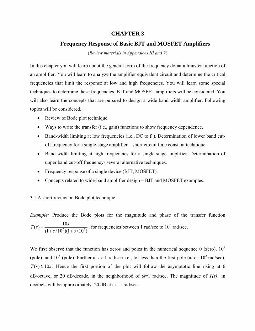
We first observe that the function has zeros and poles in the numerical sequence 0 (zero), 102
(pole), and 105 (pole). Further at ω=1 rad/sec i.e., lot less than the first pole (at ω=102 rad/sec),
( ) 10T s s . Hence the first portion of the plot will follow the asymptotic line rising at 6
dB/octave, or 20 dB/decade, in the neighborhood of ω=1 rad/sec. The magnitude of T(s) in
decibels will be approximately 20 dB at ω= 1 rad/sec.
The second asymptotic line will commence at the pole of ω=102 rad/sec, running at -6 dB/octave
slope relative to the previous asymptote. Thus the overall asymptote will be a line of slope zero,
i.e., a line parallel to the ω- axis.
The third asymptote will commence at the pole ω=105 rad/sec, running at -6 dB/Octave slope
relative to the previous asymptote. The overall asymptote will be a line dropping off at -6
dB/octave beginning from ω=105 rad/sec.
Since we have covered all the poles and zeros, we need not work on sketching any further
asymptotes. The three asymptotic lines are now sketched as shown in figure 3.1.
Figure 3.1: The asymptotic line plots for the T(s).
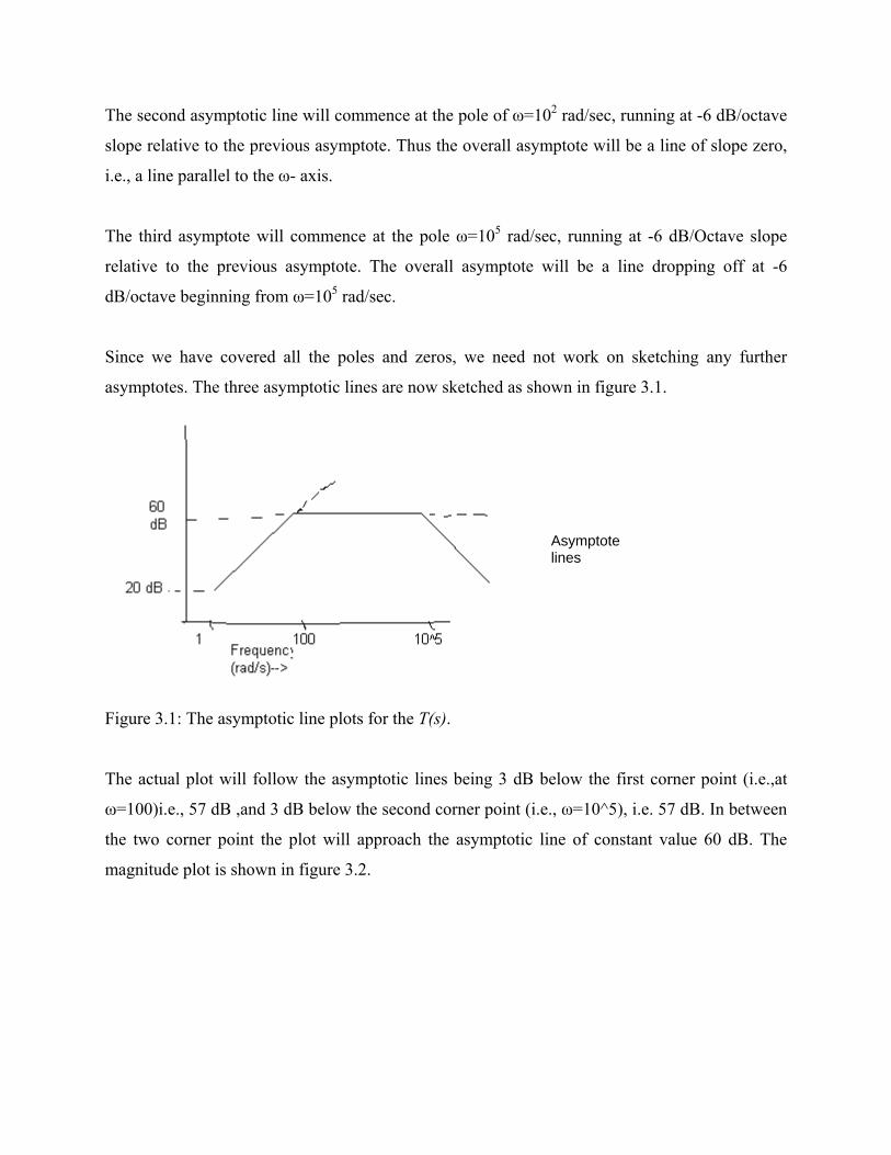
The actual plot will follow the asymptotic lines being 3 dB below the first corner point (i.e.,at
ω=100)i.e., 57 dB ,and 3 dB below the second corner point (i.e., ω=10^5), i.e. 57 dB. In between
the two corner point the plot will approach the asymptotic line of constant value 60 dB. The
magnitude plot is shown in figure 3.2.
Asymptote lines
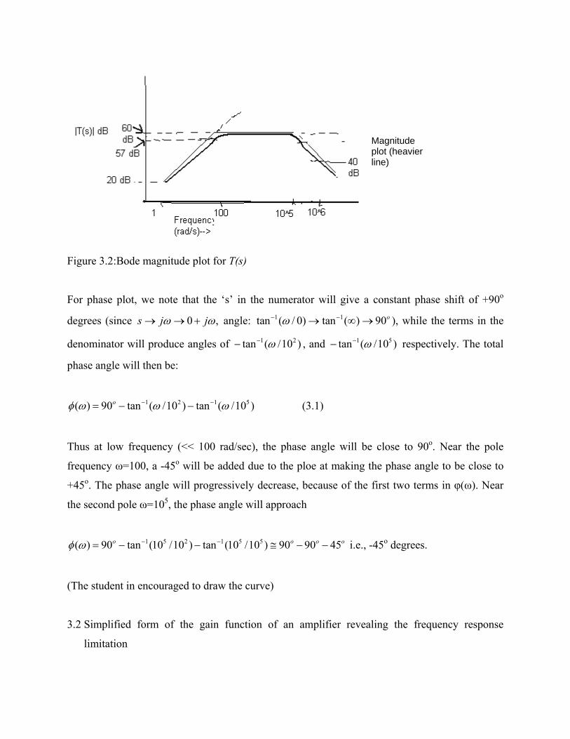
Figure 3.2:Bode magnitude plot for T(s)
For phase plot, we note that the ‘s’ in the numerator will give a constant phase shift of +90o
degrees (since 0 ,s j j angle: 1 1tan ( / 0) tan ( ) 90o ), while the terms in the
denominator will produce angles of 1 2tan ( /10 ) , and 1 5tan ( /10 ) respectively. The total
phase angle will then be:
1 2 1 5( ) 90 tan ( /10 ) tan ( /10 )o (3.1)
Thus at low frequency (<< 100 rad/sec), the phase angle will be close to 90o. Near the pole
frequency ω=100, a -45o will be added due to the ploe at making the phase angle to be close to
+45o. The phase angle will progressively decrease, because of the first two terms in φ(ω). Near
the second pole ω=105, the phase angle will approach
1 5 2 1 5 5( ) 90 tan (10 /10 ) tan (10 /10 ) 90 90 45o o o o i.e., -45o degrees.
(The student in encouraged to draw the curve)
3.2 Simplified form of the gain function of an amplifier revealing the frequency response
limitation
Magnitude plot (heavier line)
3.2.1 Gain function at low frequencies
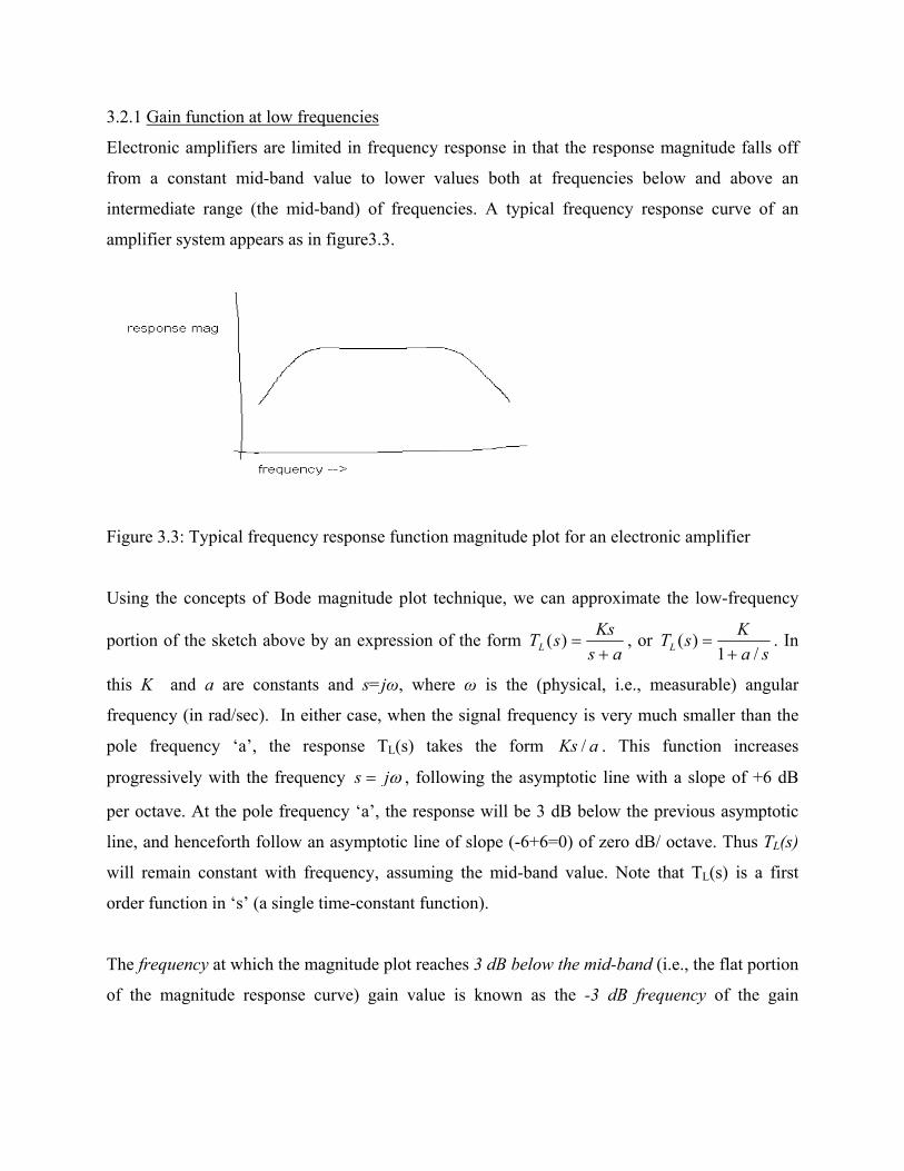
Electronic amplifiers are limited in frequency response in that the response magnitude falls off
from a constant mid-band value to lower values both at frequencies below and above an
intermediate range (the mid-band) of frequencies. A typical frequency response curve of an
amplifier system appears as in figure3.3.
Figure 3.3: Typical frequency response function magnitude plot for an electronic amplifier
Using the concepts of Bode magnitude plot technique, we can approximate the low-frequency
portion of the sketch above by an expression of the form as
KssTL )( , or
sa
KsTL /1)(
. In
this K and a are constants and s=jω, where ω is the (physical, i.e., measurable) angular
frequency (in rad/sec). In either case, when the signal frequency is very much smaller than the
pole frequency ‘a’, the response TL(s) takes the form aKs / . This function increases
progressively with the frequency js , following the asymptotic line with a slope of +6 dB
per octave. At the pole frequency ‘a’, the response will be 3 dB below the previous asymptotic
line, and henceforth follow an asymptotic line of slope (-6+6=0) of zero dB/ octave. Thus TL(s)
will remain constant with frequency, assuming the mid-band value. Note that TL(s) is a first
order function in ‘s’ (a single time-constant function).
The frequency at which the magnitude plot reaches 3 dB below the mid-band (i.e., the flat portion
of the magnitude response curve) gain value is known as the -3 dB frequency of the gain
function. For the low-frequency segment (i.e., TL(s)) of the magnitude plot this will be
designated by fL (or ωL =2π fL).
In a practical case the function TL(s) may have several poles and zeros at low frequencies. The
pole which is closest to the flat mid-band value is known as the low frequency dominant pole of
the system. Thus it is the pole of highest magnitude among all the poles and zeros at low
frequencies. Numerically the dominant pole differs from the -3 dB frequency. But for simplicity,
one can approximate dominant pole to be of same value as the -3dB frequency. The -3dB
frequency at low frequencies is also sometimes referred to as the lower cut-off frequency of the
amplifier system.
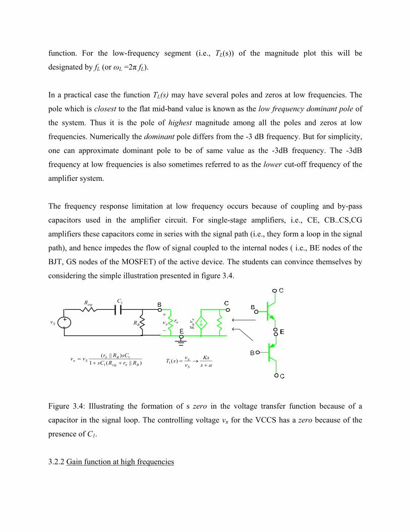
The frequency response limitation at low frequency occurs because of coupling and by-pass
capacitors used in the amplifier circuit. For single-stage amplifiers, i.e., CE, CB..CS,CG
amplifiers these capacitors come in series with the signal path (i.e., they form a loop in the signal
path), and hence impedes the flow of signal coupled to the internal nodes ( i.e., BE nodes of the
BJT, GS nodes of the MOSFET) of the active device. The students can convince themselves by
considering the simple illustration presented in figure 3.4.
sigR
BR r
vSv
1C
vg m
)||(1
)||(
1
1
Bsig
BS RrRsC
sCRrvv
as
Ks
v
vsT
S )(1
Figure 3.4: Illustrating the formation of s zero in the voltage transfer function because of a
capacitor in the signal loop. The controlling voltage vπ for the VCCS has a zero because of the
presence of C1.
3.2.2 Gain function at high frequencies
A similar scenario exists for the response at high frequencies. By considering the graph in
Fig.3.3 at frequencies beyond (i.e., higher than) the mid-band segment, we can propose the form
of the response function as: bs
KsTH )( . K and b are constants. Other alternative forms are:
bs
bKsT o
H )( , or
bs
KsT o
H /1)(
. Note that in all cases, for frequencies << the pole frequency
‘b’, the response function assumes a constant value (i.e., the mid-band response). For TH(s),
which is a first-order function, the frequency b becomes the -3db frequency for high frequency
response, or the upper cut-off frequency. When there are several poles and zeros in the high
frequency range, the pole with the smallest magnitude and hence closest to the mid-band
response zone is referred to as the high frequency dominant pole. Again, numerically the high
frequency dominant pole will be different from the upper cut-off frequency. But in most practical
cases, the difference is small. In case the high frequency response has several poles and zeros,
one can formulate the function as
1 2
1 2
(1 / )(1 / )..( )
(1 / )(1 / )..z z
Hp p
s sT s
s s
(3.2)
In an integrated circuit scenario coupling or by-pass capacitors are absent. The frequency
dependent gain function (i.e., transfer function) is produced because of the intrinsic capacitances
(parasitic capacitances) of the devices. As a consequence the zeros occur at very high
frequencies and only one of the poles fall in the signal frequency range of interest, with the other
poles at substantially higher frequencies. Thus if 1p is the pole of smallest magnitude, the
amplifier will have 1p as the dominant pole. In such case 1
1
( ) pH
p
T ss
, and 1p will also be
the -3 dB or upper cut-off frequency of the system. Otherwise, the -3 dB frequency H can be
calculated using the formula1
1/ 22 2 2 2
1 2 1 2
11 1 1 1
[( ...) 2( ..)]H
p p z z
(3.3)
3.2.3 Simplified (first order) form of the amplifier gain function
1 Sedra and Smith, “Microelectronic Circuits”, 6th edn., ch.9, p.722, Oxford University Press, ©2010.
Considering the discussions in sections 3.2.1-2 we can formulate the simplified form of the
amplifier gain function can then be considered as :
A(s)=AM FL(s) FH(s) (3.4)
In (3.4), AM is independent of frequency, FL has a frequency dependence of the form s/(s+wL),
while FH has a frequency dependence of the form wH/(s+wH). Thus for frequencies higher than
wL and for frequencies lower than wH the gain is close to AM. This is a constant gain and the
frequency band wH - wL is called the mid-band frequencies. So in the mid-band frequencies the
gain is constant i.e., AM. At frequencies << wL, FL(s) increases with frequency (re: Bode plot) by
virtue of the ‘s’ in the numerator, at 6dB/octave. As the frequency increases, the rate of increase
slows down and the Bode plot merges with the constant value AM shortly after w=wL. At w=wL
the response falls 3 dB below the initial asymptotic line of slope 6dB/octave. Similarly, as
frequency increases past wH , the response A(s) tends to fall off, passing through 3dB below AM
(in dB) at w=wH and then following the asymptotic line with slope minus 6dB/octave drawn at
w=wH . It is of interest to be able to find out these two critical frequencies for basic single stage
amplifiers implemented using BJT or MOSFET.
3.3 Simplified high-frequency ac equivalent circuits for BJT and MOSFET devices
It can be noted that for amplifiers implemented in integrated circuit technology only the upper
cut-off frequency wH is of interest. To investigate this we must be familiar with the ac equivalent
circuit of the transistor at high frequencies. The elements that affect the high frequency behavior
are the parasitic capacitors that exist in a transistor. These arise because a transistor is made by
laying down several semiconductor layers of different conductivity (i.e., p-type and n-type
materials). At the junction of each pair of dissimilar layers, a capacitance is generated. We will
consider the simplified high-frequency equivalent circuits for the BJT and MOSFET as shown in
Figs.3.5-3.6. In these models each transistor is assigned with only two parasitic capacitance
associated with its internal nodes. These arise out of the semiconductor junctions that are
involved in building the transistor. For the BJT, the base material produces a small resistance rx,
which assumes importance for high (signal) frequency applications (signal processing). The
models for N-type (i.e., NPN, NMOSFET) and P-type (i.e., PNP, PMOSFET) transistors are
considered same. In more advanced models (used in industries) more number of parasitic
capacitances and resistances are employed.
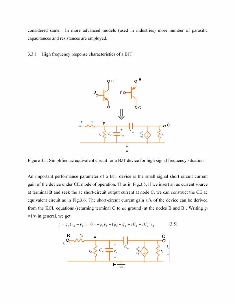
3.3.1 High frequency response characteristics of a BJT
Xr
r C C vg m or
v
Figure 3.5: Simplified ac equivalent circuit for a BJT device for high signal frequency situation.
An important performance parameter of a BJT device is the small signal short circuit current
gain of the device under CE mode of operation. Thus in Fig.3.5, if we insert an ac current source
at terminal B and seek the ac short-circuit output current at node C, we can construct the CE ac
equivalent circuit as in Fig.3.6. The short-circuit current gain io/ii of the device can be derived
from the KCL equations (returning terminal C to ac ground) at the nodes B and B’. Writing gi
=1/ri in general, we get
vsCsCggvgvvgi xBxBxi )(0),( (3.5)
Xr
r C C vg
m or
v
ii
oi
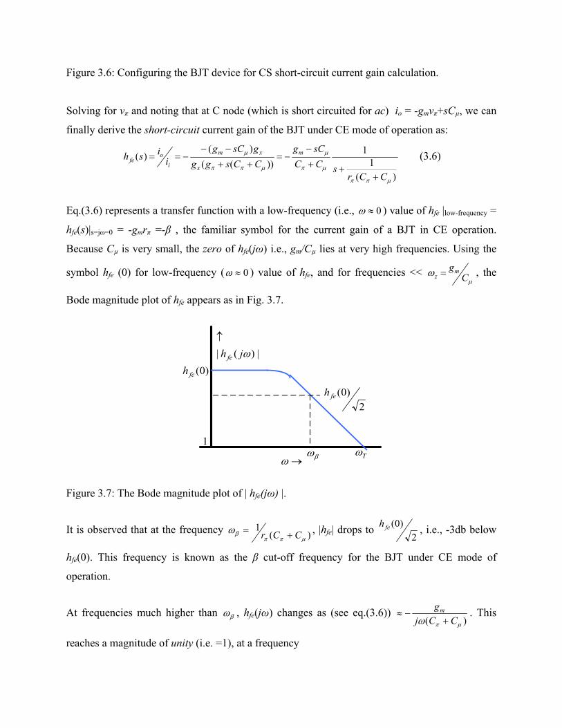
Figure 3.6: Configuring the BJT device for CS short-circuit current gain calculation.
Solving for vπ and noting that at C node (which is short circuited for ac) io = -gmvπ+sCµ, we can
finally derive the short-circuit current gain of the BJT under CE mode of operation as:
)(
11
))((
)()(
CCrsCC
sCg
CCsgg
gsCgi
ish m
x
xm
i
ofe
(3.6)
Eq.(3.6) represents a transfer function with a low-frequency (i.e., 0 ) value of hfe |low-frequency =
hfe(s)|s=jω=0 = -gmrπ =-β , the familiar symbol for the current gain of a BJT in CE operation.
Because Cµ is very small, the zero of hfe(jω) i.e., gm/Cµ lies at very high frequencies. Using the
symbol hfe (0) for low-frequency ( 0 ) value of hfe, and for frequencies <<
Cgm
z , the
Bode magnitude plot of hfe appears as in Fig. 3.7.
T
)0(feh
2)0(feh
1
|)(| jh fe
Figure 3.7: The Bode magnitude plot of | hfe(jω) |.
It is observed that at the frequency )(1
CCr , |hfe| drops to
2)0(feh
, i.e., -3db below
hfe(0). This frequency is known as the β cut-off frequency for the BJT under CE mode of
operation.
At frequencies much higher than , hfe(jω) changes as (see eq.(3.6)) )( CCj
gm
. This
reaches a magnitude of unity (i.e. =1), at a frequency
)( CC
gmT (3.7)
This is known as the transition frequency of the BJT for operation as CE amplifier. The
transition frequency TT f 2 is a very important parameter of the BJT for high-frequency
applications. For a given BJT, the high-frequency operational limit of the device can be
increased by increasing ωT via an increase in gm , the ac transconductance of the BJT. This,
however, implies an increase in the DC bias current (since gm = I/VT) and hence an increase in
the DC power consumption of the system. Recalling the relation gmrπ =β+1, we can deduce that
))0(1()1( feT h (3.8)
In real BJT devices CCCCC and, . Hence, the zero frequency
Cgm
z will be
>> the transition frequency ωT. Since |hfe(jω)| becomes <1 beyond ωT, the zero frequency bears
no practical interest.
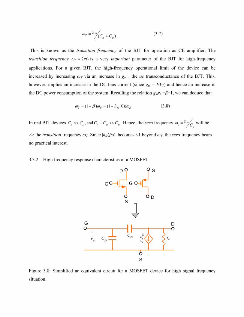
3.3.2 High frequency response characteristics of a MOSFET
G
S
gsC gdC gsm
vg
or
D
D
D
G G
S
S
gsv
Figure 3.8: Simplified ac equivalent circuit for a MOSFET device for high signal frequency
situation.
A simplified ac equivalent circuit for the MOSFET is shown in figure 3.8. The body terminal (B)
for the MOSFET , and the associated parasitic capacitances as well as the body transconductance
(gmb) have not been shown. By following a procedure similar to that of a BJT, it can be shown
that the short circuit current gain of the MOSFET configured as a CS amplifier is given by
)( gdgs
gdm
i
o
CCs
sCgi
i
which can be approximated as )( gdgs
m
i
o
CCs
g
i
i
for frequencies well below
the zero frequency gm/sCgd.
Under the above assumption the frequency at which the magnitude of the current gain becomes
unity i.e., the transition frequency, becomes:
)( gdgs
mT CC
g
(3.9)
The transition frequency of a MOSFET is a very important parameter for high frequency
operation. This can be increased via an increase in gm with the attendant increase in the DC bias
current and hence increase in DC power dissipation.
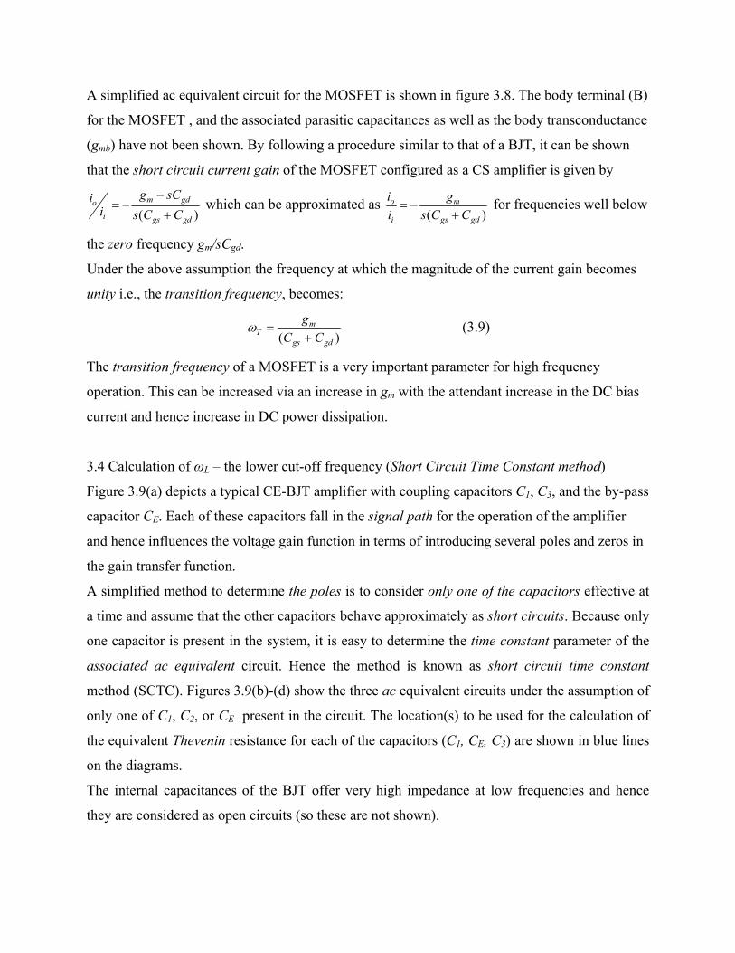
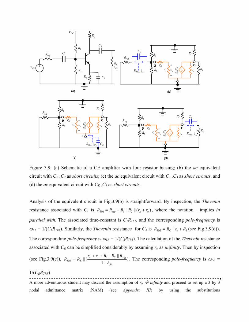
3.4 Calculation of ωL – the lower cut-off frequency (Short Circuit Time Constant method)
Figure 3.9(a) depicts a typical CE-BJT amplifier with coupling capacitors C1, C3, and the by-pass
capacitor CE. Each of these capacitors fall in the signal path for the operation of the amplifier
and hence influences the voltage gain function in terms of introducing several poles and zeros in
the gain transfer function.
A simplified method to determine the poles is to consider only one of the capacitors effective at
a time and assume that the other capacitors behave approximately as short circuits. Because only
one capacitor is present in the system, it is easy to determine the time constant parameter of the
associated ac equivalent circuit. Hence the method is known as short circuit time constant
method (SCTC). Figures 3.9(b)-(d) show the three ac equivalent circuits under the assumption of
only one of C1, C2, or CE present in the circuit. The location(s) to be used for the calculation of
the equivalent Thevenin resistance for each of the capacitors (C1, CE, C3) are shown in blue lines
on the diagrams.
The internal capacitances of the BJT offer very high impedance at low frequencies and hence
they are considered as open circuits (so these are not shown).
sigv
sigR 1C
EC
3C1R
2R
ER
CR
LR
CCV
sigv
sigRCR
LR
v or2RXr
r
vg
m
1R
ECECThevR |
sigRCR
LR
v or2RXr
r
vg
m
1R
3|CThevR
3C
sigRCR
LR
v or2RXr
r
vg
m
1R
1|CThevR
1C
Figure 3.9: (a) Schematic of a CE amplifier with four resistor biasing; (b) the ac equivalent
circuit with CE ,C3 as short circuits; (c) the ac equivalent circuit with C1 ,C3 as short circuits, and
(d) the ac equivalent circuit with CE ,C1 as short circuits.
Analysis of the equivalent circuit in Fig.3.9(b) is straightforward. By inspection, the Thevenin
resistance associated with C1 is )(|||| 211 rrRRRR xsigTh , where the notation || implies in
parallel with. The associated time-constant is C1RTh1, and the corresponding pole-frequency is
L1 = 1/(C1RTh1). Similarly, the Thevenin resistance for C3 is LoCTh RrRR ||3 (see Fig.3.9(d)).
The corresponding pole-frequency is L3 = 1/(C3RTh3). The calculation of the Thevenin resistance
associated with CE can be simplified considerably by assuming ro as inifinity. Then by inspection
(see Fig.3.9(c)), )1
||||(|| 21
fe
sigxEThE h
RRRrrRR
. The corresponding pole-frequency is LE =
1/(CERThE).
A more adventurous student may discard the assumption of ro infinity and proceed to set up a 3 by 3
nodal admittance matrix (NAM) (see Appendix III) by using the substitutions
Lccpsigspxp RRRRRRRrrr ||,||||, 21 , and by inserting a dummy current source ix at the node
labeled as E in Fig. 3.9(c). The NAM will appear as
vg
vgi
V
V
V
ggg
ggg
ggggg
m
mx
C
B
E
cpoo
sppp
opopE
0
0
0 (3.10)
In the above gE =1/RE,, gπp=1/rπp, go =1/ro, and so on, have been used. With the further assumption (it is
very good if rx is << rπ) of EB VVv , the matrix equation (3.10), becomes, after rearrangement (i.e.,
changing sides):
0
0
0
0x
C
B
E
cpommo
sppp
ompmopE i
V
V
V
ggggg
ggg
ggggggg
(3.11)
Then RThE is given by VE/ix. The result is (using Maple program code):
cpspmcpspocppocpspposppcpspEospEcppEopE
cposppThE ggggggggggggggggggggggggggg
ggggR
))((
Now introducing the assumption go0 (i.e., ro infinity), one will get
cpspmcpsppcpspEcppE
cpsppThE gggggggggggg
gggR
)( (3.12)
Substituting back in terms of the resistance notations, i.e., gE =1/RE,, gπp=1/rπp, go =1/ro, and so on, one
can get
EpmEpsp
EpspThE RrgRrR
RrRR
)( (3.13)
Using gm rπp =hfe, and simplifying, one arrives at Efepsp
feEpspThE RhrR
hRrRR
)1/()(
)1/()(
, i.e.,
)
1(||
fe
pspEThE h
rRRR )
1
||||(|| 21
fe
sigxE h
RRRrrR
.
********
The overall lower -3 dB frequency is calculated approximately by the formula
LELLL 31 . If out of the several poles of the low-frequency transfer function FL(s), one
is very large compared to all other poles and zeros, the overall lower -3 dB frequency L
becomes dominant pole (i.e., largest of L1 or LE or L3).
If the numerical values of the various pole frequencies are known (by exact circuit analysis
followed by numerical computation), the lower 3-dB frequency can be calculated approximately
by a formula of the form ...23
22
21 L where, ω1, ω2 , .. are the individual pole
frequencies and the zero-frequencies are very small compared with the pole frequencies.
Example 3.4.1: Consider the following values in a BJT amplifier.
Rsig =50, RB=R1||R2 = 10 k, r =2500, rx =25, hfe =100 and RE =1k, RC =1.5k, RL =3.3
k, VA =20 volts, IC 1 mA. Further, C1 =1uF and CE= 10uF and C3 = 1uF. What is L ?
According to above formulas, RTh1 = 2.05k , RThE =25.25 and RTh3 =1.39k+3.3k =
4.69k. Then L1 = 487.8 rad/s, LE = 3.96E3 rad/sec and L3 = 213.2 rad/sec. Then ,
2 2 2487.8 3.96 3 213.2 3.9956 3L E E , which is pretty close to LE.
Example 3.4.2: What if , L= 1800 rad/sec is to be designed? We can assume, for example, L1 =
0.8L, , ωLE= L2= 0.1L and L3=0.1L. Then, design the values of the capacitors C1, CE and
C3. The student can try other relative allocations too.
3.5: Calculation of ωH – the higher cut-off frequency
Several alternative methods exist in the literature. The following are presented.
3.5.1 Open circuit time-constant (OCTC) method
This is similar to the case as with low frequency response. For high frequency operation, we are
interested in the capacitor which will have lower reactance value since this capacitance will start
to degrade the high frequency response sooner than the other. Thus, we can consider one
capacitor at a time and assume that the other capacitors are too small and have reasonably high
reactance values (for a C, the reactance is 1/C) so that they could be considered as open
circuits. We then calculate the associated time constant. Thus the method is named as open
circuit time constant (OCTC) method. We shall illustrate the method using the case of a CE BJT
amplifier.
Consider figure 3.10(a) which shows the ac equivalent circuit of the CE-BJT amplifier of
Fig.3.9(a). The high frequency equivalent circuit for the BJT has been included. The coupling
and by-pass capacitors are assumed as short circuits for high frequency situation.
sigR CR
C
v2RB
E
Xr
r
1R
+-
LRor
vg
mC
CsigR CR
C
v2RB
E
Xr
r
1R
LRor
vg
mC
ThR
sigR CR
C
v2RB
E
Xr
r
1R
LRor
vg
m
C
ThR
(a) (b)
(c)
Figure 3.10: (a) high frequency equivalent circuit of the amplifier in Fig.3.9(a); (b) the
equivalent circuit with Cµ open; (c) the equivalent circuit with Cπ open.
Case 1: C open
The ac equivalent circuit to determine the Thevenin equivalent resistance RThπ across Cπ is shown
in Fig.3.10(b). By simple inspection )||||(|| 21 RRRrrR sigxTh
The high frequency pole due to this situation is H1 =1/(Cπ RThπ).
Case 2: Cπ open
We now need to determine the Thevenin equivalent resistance RThµ across Cµ. The associated
equivalent circuit is shown in Fig.3.10(c). We can use a dummy signal current source ix and carry
out few steps of basic circuit analysis (see Fig.3.11).
CR
C
1V
sig
RR
R||
||1
2
B
E
Xr
r LRor
1Vg
m
xi
2V
Figure 3.11: Equivalent circuit for calculating RThµ
KCL at V1 node gives: Ssigx
SxS RRRRrrGiGV
1
)||||(||
1,0
211
(3.13a)
KCL at V2 node gives: LLCo
LLmx RRRrGGVVgi 1
||||
1,021 (3.13b)
Solving (3.13(a),(b)) for V1 and V2 we can find RThµ =(V2-V1)/ix = Rs’+(1+gmRs’)RL’
The high frequency pole for C is H2 = 1/ CRThµ.
When the two pole frequencies are comparable in values, the upper -3 dB frequency is given
approximately by )(1
)(1
21
ThThH RCRC (3.14)
If, however, the two values are widely apart (say, by a factor of 5 or more), the upper -3 dB
frequency will be called as the dominant high frequency pole and will be equal to the lesser of
H1 and H2.
3.5.2 Application of Miller’s theorem
This theorem helps simplifying the ac equivalent circuit of the BJT CE amplifier by removing
the C capacitor, which runs between two floating nodes (i.e., between the base side to the
collector side). In principle, if an admittance Y3 runs between nodes 1 and 2 with Y1 at node 1
(to ground) and Y2 at node 2 (and ground) and if K is the voltage gain (V2/V1) between nodes 1
and 2, then Y3 can be split into two parts – one being in parallel with Y1 with a value Y3 (1-K)
and another becoming in parallel with Y2 with a value (1-1/K)Y3. The theorem can be applied to
all cases of floating elements connected between two nodes in a system.
As a result of this principle, the high frequency equivalent circuit of the CE BJT amplifier (see
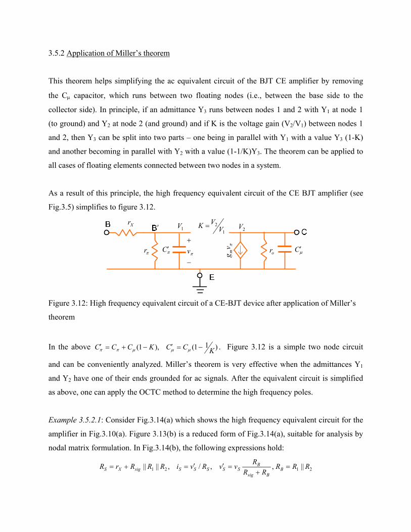
Fig.3.5) simplifies to figure 3.12.
Xr
r C C
vg
m or
v
1V 2V1
2V
VK
Figure 3.12: High frequency equivalent circuit of a CE-BJT device after application of Miller’s
theorem
In the above )11(),1( KCCKCCC . Figure 3.12 is a simple two node circuit
and can be conveniently analyzed. Miller’s theorem is very effective when the admittances Y1
and Y2 have one of their ends grounded for ac signals. After the equivalent circuit is simplified
as above, one can apply the OCTC method to determine the high frequency poles.
Example 3.5.2.1: Consider Fig.3.14(a) which shows the high frequency equivalent circuit for the
amplifier in Fig.3.10(a). Figure 3.13(b) is a reduced form of Fig.3.14(a), suitable for analysis by
nodal matrix formulation. In Fig.3.14(b), the following expressions hold:
2121 ||,,/,|||| RRRRR
RvvRviRRRrR B
Bsig
BSSSSSsigXS
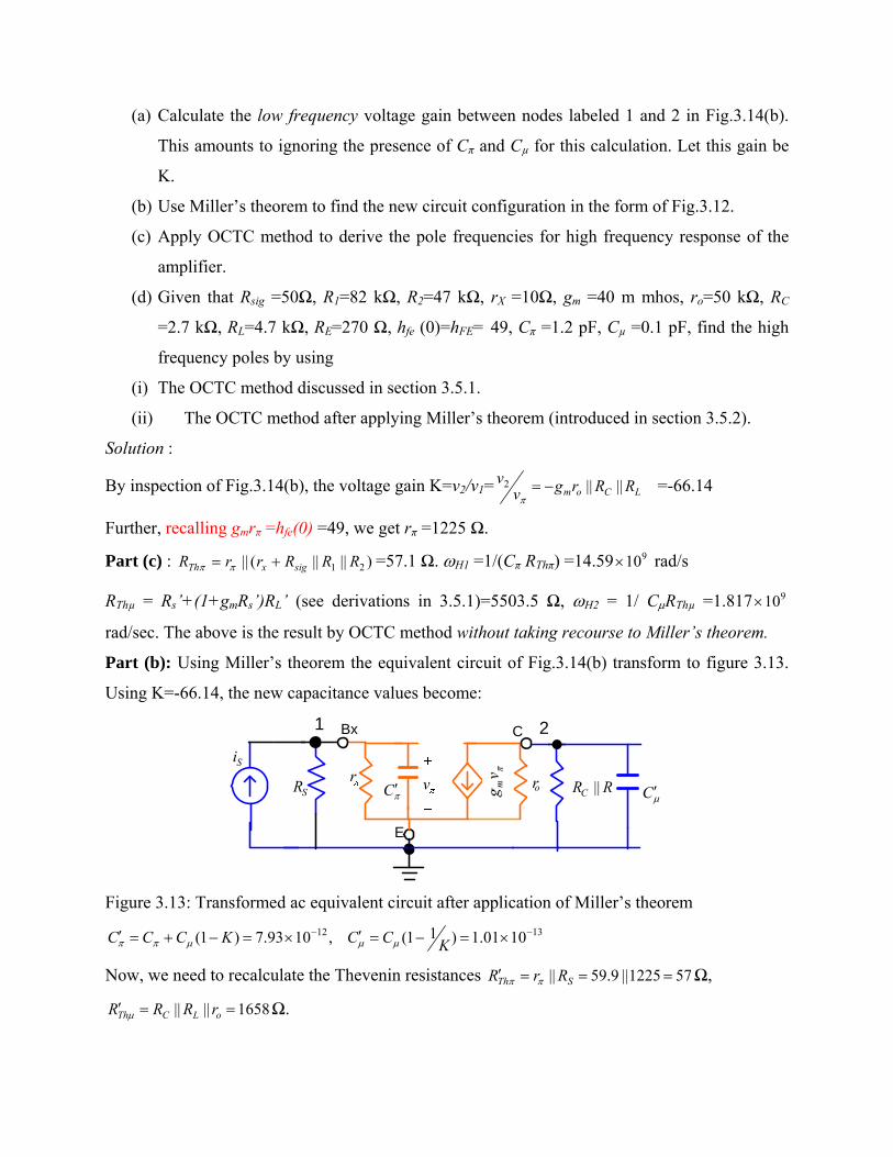
(a) Calculate the low frequency voltage gain between nodes labeled 1 and 2 in Fig.3.14(b).
This amounts to ignoring the presence of Cπ and Cµ for this calculation. Let this gain be
K.
(b) Use Miller’s theorem to find the new circuit configuration in the form of Fig.3.12.
(c) Apply OCTC method to derive the pole frequencies for high frequency response of the
amplifier.
(d) Given that Rsig =50Ω, R1=82 kΩ, R2=47 kΩ, rX =10Ω, gm =40 m mhos, ro=50 kΩ, RC
=2.7 kΩ, RL=4.7 kΩ, RE=270 Ω, hfe (0)=hFE= 49, Cπ =1.2 pF, Cµ =0.1 pF, find the high
frequency poles by using
(i) The OCTC method discussed in section 3.5.1.
(ii) The OCTC method after applying Miller’s theorem (introduced in section 3.5.2).
Solution :
By inspection of Fig.3.14(b), the voltage gain K=v2/v1= LCom RRrgvv ||||2
=-66.14
Further, recalling gmrπ =hfe(0) =49, we get rπ =1225 Ω.
Part (c) : )||||(|| 21 RRRrrR sigxTh =57.1 Ω. H1 =1/(Cπ RThπ) =14.59 910 rad/s
RThµ = Rs’+(1+gmRs’)RL’ (see derivations in 3.5.1)=5503.5 Ω, H2 = 1/ CRThµ =1.817 910
rad/sec. The above is the result by OCTC method without taking recourse to Miller’s theorem.
Part (b): Using Miller’s theorem the equivalent circuit of Fig.3.14(b) transform to figure 3.13.
Using K=-66.14, the new capacitance values become:
C
v
Bx
E
rC RR ||or
Si
SR
1 2
C C
Figure 3.13: Transformed ac equivalent circuit after application of Miller’s theorem
1312 1001.1)11(,1093.7)1( KCCKCCC
Now, we need to recalculate the Thevenin resistances 571225||9.59|| STh RrR Ω,
1658|||| oLCTh rRRR Ω.
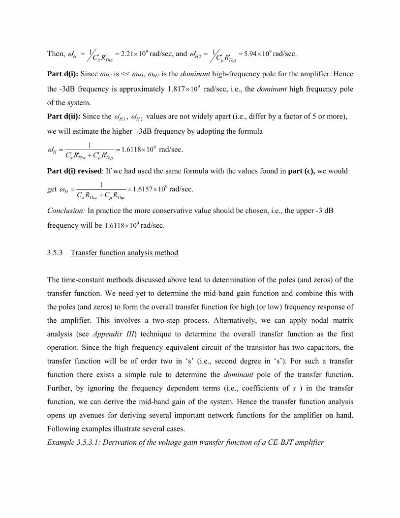
Then, 91 1021.21
ThH RC rad/sec, and 9
2 1094.51
Th
H RC rad/sec.
Part d(i): Since H2 is << H1, H2 is the dominant high-frequency pole for the amplifier. Hence
the -3dB frequency is approximately 1.817 910 rad/sec, i.e., the dominant high frequency pole
of the system.
Part d(ii): Since the 1H , 2H values are not widely apart (i.e., differ by a factor of 5 or more),
we will estimate the higher -3dB frequency by adopting the formula
9106118.11
ThTh
H RCRC rad/sec.
Part d(i) revised: If we had used the same formula with the values found in part (c), we would
get 9106157.11
ThTh
H RCRCrad/sec.
Conclusion: In practice the more conservative value should be chosen, i.e., the upper -3 dB
frequency will be 9106118.1 rad/sec.
3.5.3 Transfer function analysis method
The time-constant methods discussed above lead to determination of the poles (and zeros) of the
transfer function. We need yet to determine the mid-band gain function and combine this with
the poles (and zeros) to form the overall transfer function for high (or low) frequency response of
the amplifier. This involves a two-step process. Alternatively, we can apply nodal matrix
analysis (see Appendix III) technique to determine the overall transfer function as the first
operation. Since the high frequency equivalent circuit of the transistor has two capacitors, the
transfer function will be of order two in ‘s’ (i.e., second degree in ‘s’). For such a transfer
function there exists a simple rule to determine the dominant pole of the transfer function.
Further, by ignoring the frequency dependent terms (i.e., coefficients of s ) in the transfer
function, we can derive the mid-band gain of the system. Hence the transfer function analysis
opens up avenues for deriving several important network functions for the amplifier on hand.
Following examples illustrate several cases.
Example 3.5.3.1: Derivation of the voltage gain transfer function of a CE-BJT amplifier
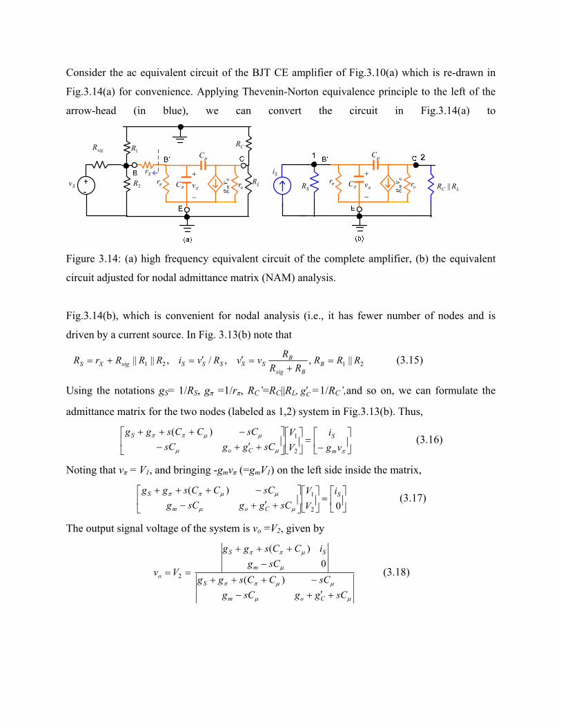
Consider the ac equivalent circuit of the BJT CE amplifier of Fig.3.10(a) which is re-drawn in
Fig.3.14(a) for convenience. Applying Thevenin-Norton equivalence principle to the left of the
arrow-head (in blue), we can convert the circuit in Fig.3.14(a) to
sigR CR
v2RXr
r
1R
LRor
vg
mC
C
Sv
vrLC RR ||or
vg
mC
C
Si
SR
Figure 3.14: (a) high frequency equivalent circuit of the complete amplifier, (b) the equivalent
circuit adjusted for nodal admittance matrix (NAM) analysis.
Fig.3.14(b), which is convenient for nodal analysis (i.e., it has fewer number of nodes and is
driven by a current source. In Fig. 3.13(b) note that
2121 ||,,/,|||| RRRRR
RvvRviRRRrR B
Bsig
BSSSSSsigXS
(3.15)
Using the notations gS= 1/RS, gπ =1/rπ, RC’=RC||RL, Cg =1/RC’,and so on, we can formulate the
admittance matrix for the two nodes (labeled as 1,2) system in Fig.3.13(b). Thus,
vg
i
V
V
sCggsC
sCCCsgg
m
S
Co
S
2
1)( (3.16)
Noting that vπ = V1, and bringing -gmvπ (=gmV1) on the left side inside the matrix,
0
)(
2
1 S
Com
S i
V
V
sCggsCg
sCCCsgg
(3.17)
The output signal voltage of the system is vo =V2, given by
2Vvo
sCggsCg
sCCCsgg
sCg
iCCsgg
Com
S
m
SS
)(
0
)(
(3.18)
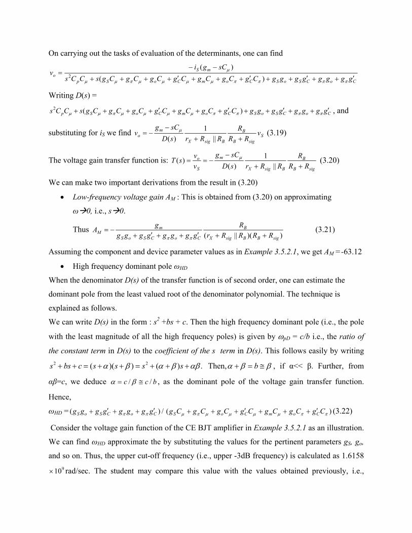
On carrying out the tasks of evaluation of the determinants, one can find
CoCSoSComCoSp
mSo
ggggggggCgCgCgCgCgCgCgsCCs
sCgiv
)(
)(2
Writing D(s) =
CoCSoSComCoSp ggggggggCgCgCgCgCgCgCgsCCs )(2 , and
substituting for iS we find SsigB
B
BsigX
mo v
RR
R
RRrsD
sCgv
||
1
)( (3.19)
The voltage gain transfer function is: sigB
B
BsigX
m
S
o
RR
R
RRrsD
sCg
v
vsT
||
1
)()( (3.20)
We can make two important derivations from the result in (3.20)
Low-frequency voltage gain AM : This is obtained from (3.20) on approximating
ω0, i.e., s0.
Thus ))(||( sigBBsigX
B
CoCSoS
mM RRRRr
R
gggggggg
gA
(3.21)
Assuming the component and device parameter values as in Example 3.5.2.1, we get AM =-63.12
High frequency dominant pole ωHD
When the denominator D(s) of the transfer function is of second order, one can estimate the
dominant pole from the least valued root of the denominator polynomial. The technique is
explained as follows.
We can write D(s) in the form : s2 +bs + c. Then the high frequency dominant pole (i.e., the pole
with the least magnitude of all the high frequency poles) is given by pD = c/b i.e., the ratio of
the constant term in D(s) to the coefficient of the s term in D(s). This follows easily by writing
2 2( )( ) ( ) .s bs c s s s s Then, b , if α<< β. Further, from
αβ=c, we deduce bcc // , as the dominant pole of the voltage gain transfer function.
Hence,
ωHD = /)( CoCSoS gggggggg )( CgCgCgCgCgCgCg ComCoS (3.22)
Consider the voltage gain function of the CE BJT amplifier in Example 3.5.2.1 as an illustration.
We can find ωHD approximate the by substituting the values for the pertinent parameters gS, go,
and so on. Thus, the upper cut-off frequency (i.e., upper -3dB frequency) is calculated as 1.6158
910 rad/sec. The student may compare this value with the values obtained previously, i.e.,
1.6157 910 rad/sec (using OCTC method), and 1.6118 910 rad/sec (using Miller’s theorem
followed by OCTC method), respectively.
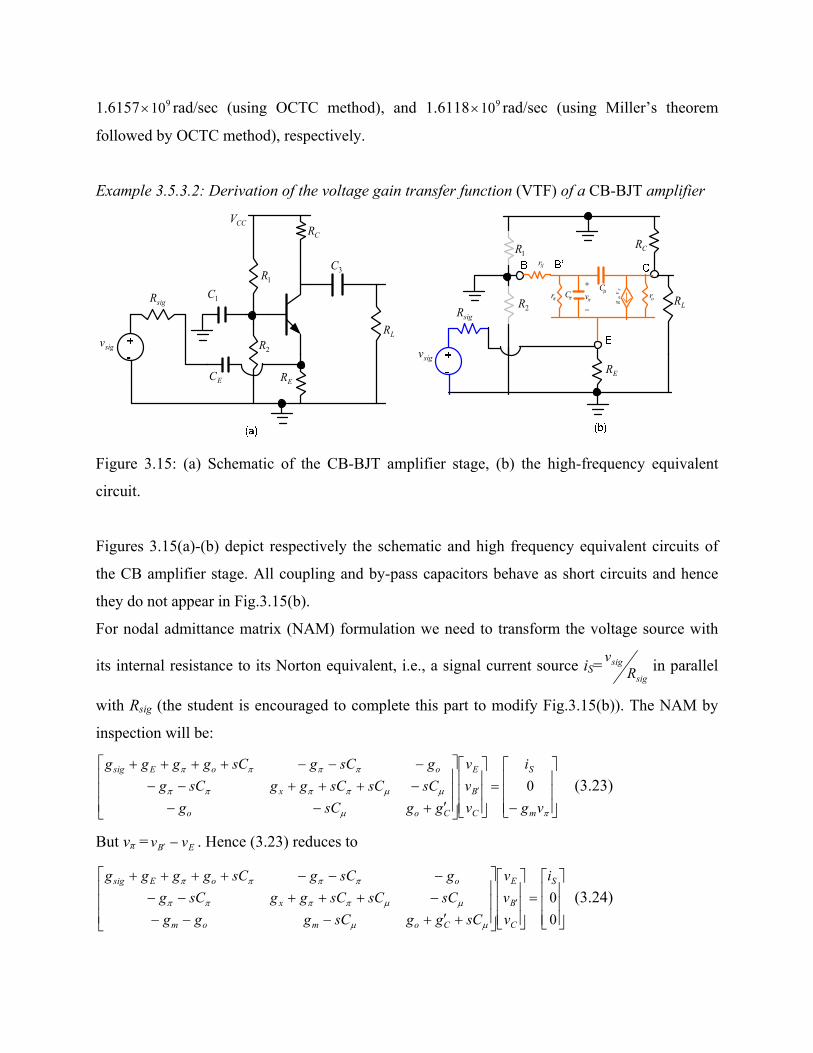
Example 3.5.3.2: Derivation of the voltage gain transfer function (VTF) of a CB-BJT amplifier
sigv
sigR 1C
EC
3C1R
2R
ER
CR
LR
CCV
sigv
CR
LR2R
1R
ER
sigR
Xr
r C C v
gm or
v
Figure 3.15: (a) Schematic of the CB-BJT amplifier stage, (b) the high-frequency equivalent
circuit.
Figures 3.15(a)-(b) depict respectively the schematic and high frequency equivalent circuits of
the CB amplifier stage. All coupling and by-pass capacitors behave as short circuits and hence
they do not appear in Fig.3.15(b).
For nodal admittance matrix (NAM) formulation we need to transform the voltage source with
its internal resistance to its Norton equivalent, i.e., a signal current source iS=sig
sig
Rv
in parallel
with Rsig (the student is encouraged to complete this part to modify Fig.3.15(b)). The NAM by
inspection will be:
vg
i
v
v
v
ggsCg
sCsCsCggsCg
gsCgsCgggg
m
S
C
B
E
Coo
x
ooEsig
0 (3.23)
But vπ = EB vv . Hence (3.23) reduces to
0
0S
C
B
E
Comom
x
ooEsig i
v
v
v
sCggsCggg
sCsCsCggsCg
gsCgsCgggg
(3.24)
In order to compare the performance of the CB and CE BJT amplifiers, it will be convenient to
assume rX as negligible. Then node B’ will be at zero ac potential and (3.24) will approximate to
(by discarding the row and column associated with the B’ node)
0
S
C
E
Coom
ooEsig i
v
v
sCgggg
gsCgggg
(3.25)
The VTF is given by
vo/vsig =vC/vsig =
)()()]()([
)(2
gggggggggggggggCggCsCCs
ggg
oEsigCmCEsigoosigECo
omsig
Using the VTF we can deduce
The mid-band gain (i.e., s jω, ω0) for CB mode of operation is:
)()(
)(|
ggggggggggg
gggA
oEsigCmCEsigo
omsigCBM
(3.26)
The dominant high frequency pole for CB mode of operation is
ωHD| CB= )()(
)()(
osigECo
oEsigCmCEsigo
ggggCggC
ggggggggggg
(3.27)
Example 3.5.3.3: Determine the mid-band gains and dominant high frequency poles of the BJT
amplifier operated as CE (see Fig.3.9a) and CB (see Fig.3.15a) modes of operation. The devices,
the DC biasing conditions, and the circuit components are assumed identical for both the
configurations.
[Given Rsig =50Ω, R1=82 kΩ, R2=47 kΩ, RE=270 Ω, RC =2.7 kΩ, RL=4.7 kΩ
gm =40 m mhos, ro=50 kΩ, rX =10Ω ,hfe(0)=hFE = 49
Cπ =1.2 pF, Cµ =0.1 pF]
On substitution into the expressions (3.26) and (3.27), we get: AM =57.17 v/v, ωHD|CB=4.5796
910 rad/sec.
Note I: We observed that the CB-BJT amplifier has somewhat lower voltage gain (i.e., 57.17)
compared with that of CE-BJT (i.e., 63.12 in magnitude) amplifier, but has a higher high-
frequency bandwidth (~ dominant high-frequency pole=4.5796 910 rad/sec) compared with that
of CE-BJT (i.e., 1.6158 910 rad/sec) amplifier.
Note II: It is known that the CE-BJT amplifier as moderate to high (kΩ to tens of kΩ) input
resistance, as well as moderately high (kΩ) output resistance. In comparison, a CB-BJT amplifier
has low (Ω to tens of Ω) input resistance while a moderately high (kΩ) output resistance.
Note III: A CB-BJT is preferred over a CE-BJT amplifier for most radio-frequency (MHz and
above) applications because it has a higher high-frequency bandwidth (for identical device and
biasing conditions), and affords to provide better impedance matching at the input with the
radio-frequency (RF) source (Rsig in the range of 50Ω to 75Ω).
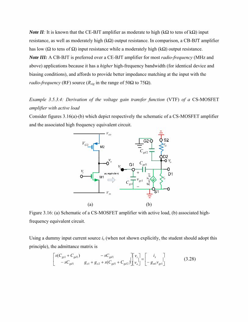
Example 3.5.3.4: Derivation of the voltage gain transfer function (VTF) of a CS-MOSFET
amplifier with active load
Consider figures 3.16(a)-(b) which depict respectively the schematic of a CS-MOSFET amplifier
and the associated high frequency equivalent circuit.
DDV
SSV
ov
iviv
2GV
1or
ov
2or
1gsC
1gdC
1gsv
11
gsm
vg
2gdC
(a) (b)
Figure 3.16: (a) Schematic of a CS-MOSFET amplifier with active load, (b) associated high-
frequency equivalent circuit.
Using a dummy input current source ix (when not shown explicitly, the student should adopt this
principle), the admittance matrix is
1121211
111
)(
)(
gsm
x
o
i
gdgdoogd
gdgdgs
vg
i
v
v
CCsggsC
sCCCs (3.28)
After re-arranging (the student is suggested to work out the details), we can find the VTF given
by
)(0
0
)(
2121
1
1
11
gdgdoo
gdx
gdm
xgdgs
i
o
CCsgg
sCi
sCg
iCCs
v
v
(3.29)
Exercise 3.5.3.4: Can you sketch the Bode magnitude plot for the above VTF? Assume, gm=250
µA/V, ro1, ro2 =1 MΩ (each), Cgd1, Cgd2= 20 fF (each f femto i.e., 10-15), Cgs1= 100 fF.
Example 3.5.3.5: Derivation of the voltage gain transfer function (VTF) of a CG-MOSFET
amplifier.
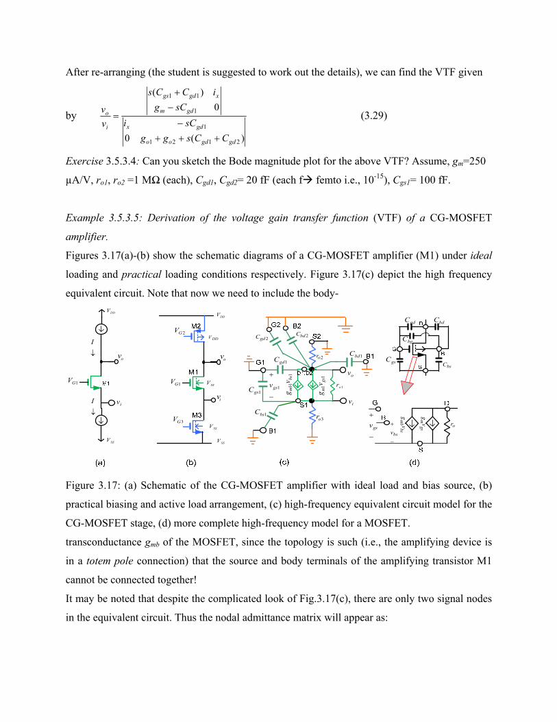
Figures 3.17(a)-(b) show the schematic diagrams of a CG-MOSFET amplifier (M1) under ideal
loading and practical loading conditions respectively. Figure 3.17(c) depict the high frequency
equivalent circuit. Note that now we need to include the body-
DDV
SSV
ov
DDV
SSV
ov
iv
2GV
1GV
iv
I
I
1GV
3GV
1or1gsC
1gdC
1gsv
11
gsm
vg
11
bsm
bv
g
1bsC
1bdC2or
2gdC 2bdC
SSV
SSV
DDV
gsC
gdC
bgC
bdC
bsC
gsv
bsvorgs
m vg
bsm
b vg
iv
ov
3or
Figure 3.17: (a) Schematic of the CG-MOSFET amplifier with ideal load and bias source, (b)
practical biasing and active load arrangement, (c) high-frequency equivalent circuit model for the
CG-MOSFET stage, (d) more complete high-frequency model for a MOSFET.
transconductance gmb of the MOSFET, since the topology is such (i.e., the amplifying device is
in a totem pole connection) that the source and body terminals of the amplifying transistor M1
cannot be connected together!
It may be noted that despite the complicated look of Fig.3.17(c), there are only two signal nodes
in the equivalent circuit. Thus the nodal admittance matrix will appear as:
1111
1111
2211211
11113
)(
)(
bsmbgsm
bsmbgsmx
o
i
gdbdgdbdooo
obsgsoo
vgvg
vgvgi
v
v
CCCCsggg
gCCsgg
Writing C1=Cgs1+Cbs1, C2=Cgd1+Cbd1+Cgd2+Cbd2, and observing that the gate and body terminals
of the MOSFETs are at zero ac potentials so that vgs1=-vs1=-vi, vbs1=-vs1=-vi, we can re-write the
admittance matrix equation as
imbim
imbimx
o
i
ooo
ooo
vgvg
vgvgi
v
v
sCggg
gsCgg
11
11
2211
1113 (3.30)
Re-arranging, we get
0221111
111113 x
o
i
ooombm
ombmoo i
v
v
sCggggg
gsCgggg (3.31)
The VTF is given by:
221
1
111
11113
0
0
sCgg
gi
ggg
isCgggg
v
v
oo
ox
ombm
xmbmoo
i
o
(3.32)
Exercise 3.5.3.5-I: Find the explicit expression for the VTF using (3.32).
Exercise 3.5.3.5-II: Using (3.31), and the knowledge that the driving point impedance (DPI) at
the input is given by x
idpi i
vZ , find the expression for the Zdpi.
Exercise 3.5.3.5-III: Given that ,2.0,200,2,1 111231 mmbmooo ggmhogMrMrr
fFCfFCfFCfFCfFCfFC bdgdbdgdbsgs 15,10,20,5,20,100 221111 find the expressions
for the VTF and the Zdpi
Exercise 3.5.3.5-IV: Find the expression for the trans-impedance function TIF (=x
oi
v ) for the
amplifier stage.
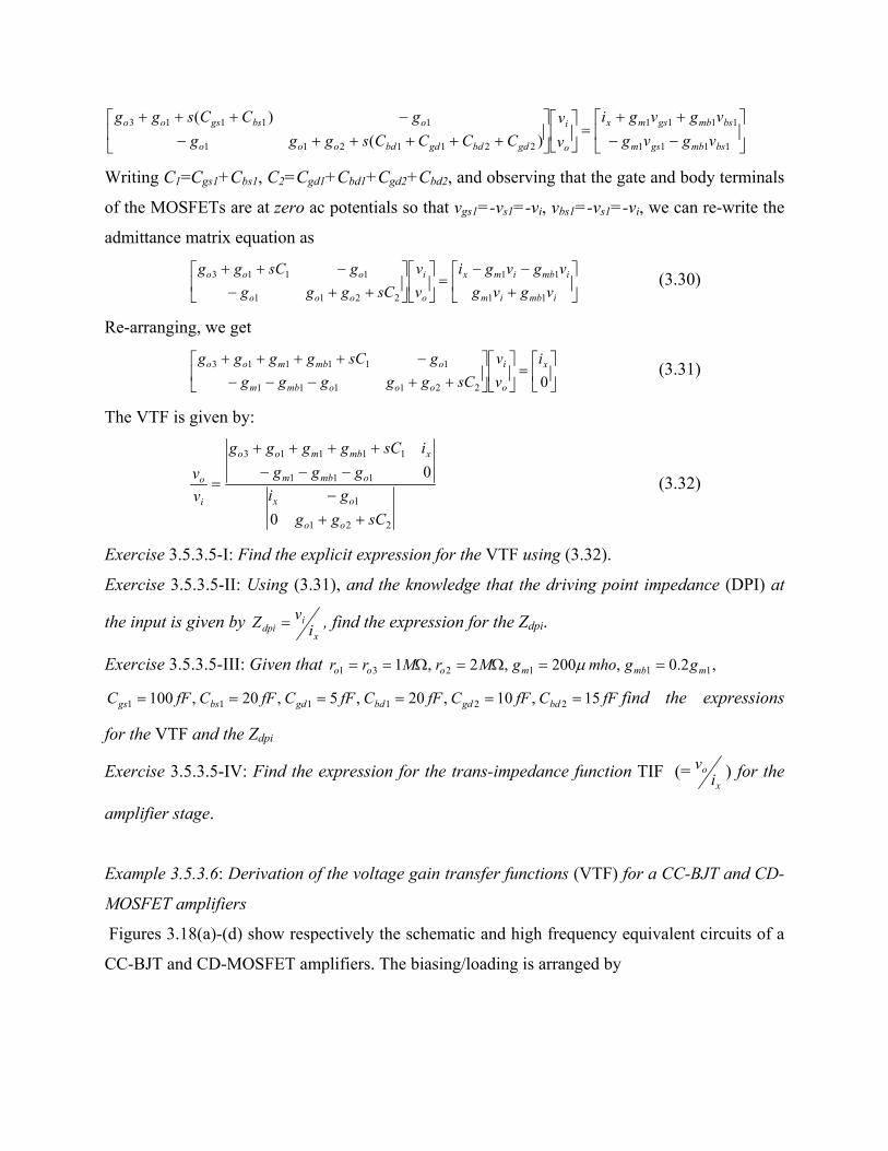
Example 3.5.3.6: Derivation of the voltage gain transfer functions (VTF) for a CC-BJT and CD-
MOSFET amplifiers
Figures 3.18(a)-(d) show respectively the schematic and high frequency equivalent circuits of a
CC-BJT and CD-MOSFET amplifiers. The biasing/loading is arranged by
SSV
DDV
sigR
sv
2GV
SSV
CCV
EEV
2BV
sigR
sv
sigR
sv
2or
1xr
1r
1C
1v
1C
11 vgm
1or
sigR
sv
2or
1gsC
1gsv1gdC
11 gsm vg
1or
11 bsmb vg
ov ov
ov
ov
Figure 3.18: (a) Schematic of a CC-BJT amplifier, (b) high frequency equivalent circuit of the
CC amplifier, (c) Schematic of a CD-MOSFET amplifier, (d) high frequency equivalent circuit
of the CD amplifier
employing active resistors (Q2 in Fig.3.18(a), and M2 in Fig.3.18(c)). It may be noted that since
one terminal of the capacitor Cµ1 (and of Cgd1) is grounded for ac, neither of these capacitors are
subjected to the Miller effect magnification, as are in the cases with CE (BJT and CS (MOSFET)
amplifiers.
The student is encouraged to complete the analysis and derive the expressions for the VTF vo/vs
of the CC and the CD amplifiers.Remember that for the MOSFET the body terminal is connected
to a DC voltage.
Created by: Rabin Raut, Ph.D. 1 2/10/2012
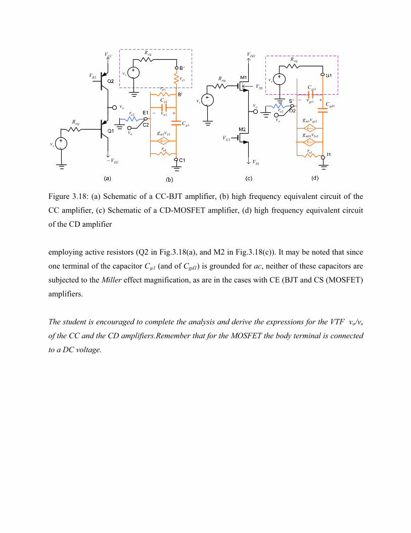
3.6: Wide band multi-stage amplifiers
3.6.1: CE-CB Cascode BJT amplifier
It has been known that a CE stage has high voltage gain and high input resistance while a
CB stage has high voltage gain with low input resistance. For high frequency operation
CE amplifier will have a smaller band width than the CB amplifier since in the former the
capacitance C is magnified due to Miller effect. This has a corresponding effect on
reducing the band width. In the CB stage, since the base is at ac ground, the capacitance
C has already one terminal to ground and is not subjected to Miller effect magnification.
So the CB stage affords to higher operating band width.
It is interesting to consider a composite amplifier containing the CE and CB stages so that
advantages of both the configurations could be shared. That is what happens in a cascode
amplifier where the CE stage receives the input signal, while the CB stage acts as a low
resistance load for the CE stage. Because of the low resistance load, the Miller effect
magnification of the C capacitor in the CE stage is drastically reduced. Because of the
low resistance load, however, the voltage gain in the CE stage drops. But it is adequately
compensated by the large voltage gain of the CB stage which works from a low input
resistance to a high output resistance.
3.6.1.1: Analysis for the bandwidth and mid-band gain
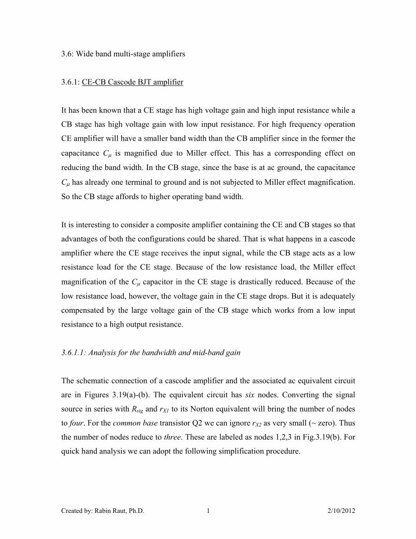
The schematic connection of a cascode amplifier and the associated ac equivalent circuit
are in Figures 3.19(a)-(b). The equivalent circuit has six nodes. Converting the signal
source in series with Rsig and rX1 to its Norton equivalent will bring the number of nodes
to four. For the common base transistor Q2 we can ignore rX2 as very small (~ zero). Thus
the number of nodes reduce to three. These are labeled as nodes 1,2,3 in Fig.3.19(b). For
quick hand analysis we can adopt the following simplification procedure.
Created by: Rabin Raut, Ph.D. 2 2/10/2012
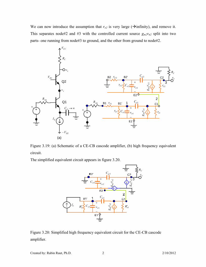
We can now introduce the assumption that ro2 is very large (infinity), and remove it.
This separates node#2 and #3 with the controlled current source gm2vπ2 split into two
parts- one running from node#3 to ground, and the other from ground to node#2.
2BV
CR
CCV
EEV
EC
ov
xv
EI
+-
sigR
sv
(a)
B2 C2
E2
B2'2Xr
2r 2C
2C
22
vg m
2or
2v
B1 C1
E1
B1'1Xr
1r 1C
1C
11
vg m
1or
1v+-
sigR
sv
CR
ov
12
3
Q1
Q2
Figure 3.19: (a) Schematic of a CE-CB cascode amplifier, (b) high frequency equivalent
circuit.
The simplified equivalent circuit appears in figure 3.20.
2C
2C
22
vg m
2v
SR 1C
1C
11
vg m 1oR
1v
CR
ov
Si
22
vg m
Figure 3.20: Simplified high frequency equivalent circuit for the CE-CB cascode
amplifier.
Created by: Rabin Raut, Ph.D. 3 2/10/2012
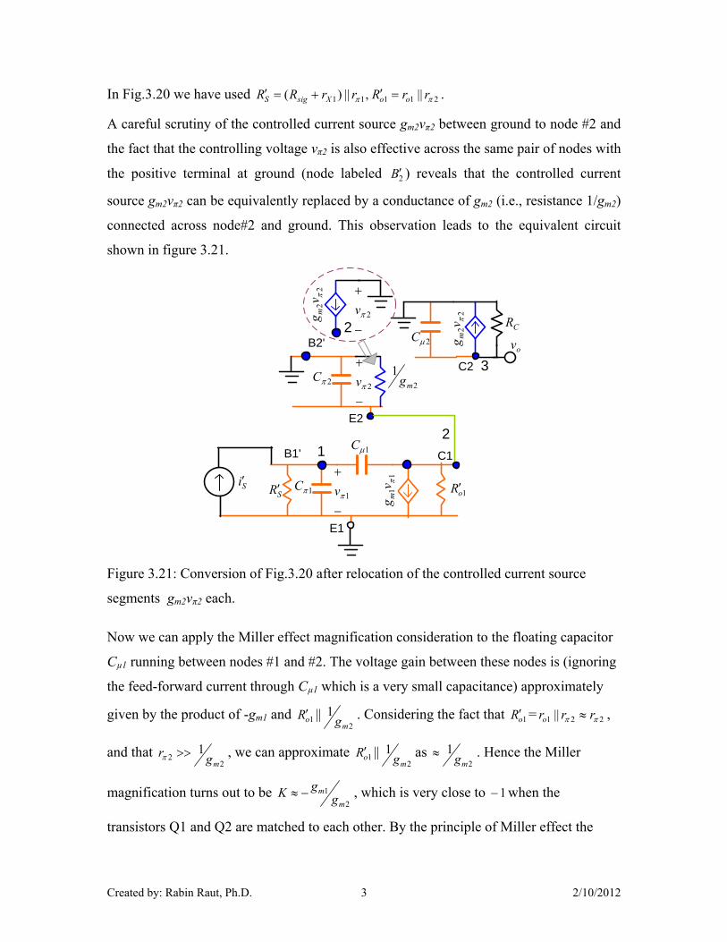
In Fig.3.20 we have used 21111 ||,||)( rrRrrRR ooXsigS .
A careful scrutiny of the controlled current source gm2vπ2 between ground to node #2 and
the fact that the controlling voltage vπ2 is also effective across the same pair of nodes with
the positive terminal at ground (node labeled 2B ) reveals that the controlled current
source gm2vπ2 can be equivalently replaced by a conductance of gm2 (i.e., resistance 1/gm2)
connected across node#2 and ground. This observation leads to the equivalent circuit
shown in figure 3.21.
C2
E2
B2'
2C
2C
22
vg m
2v
C1
E1
B1'
SR 1C
1C
11
vg m
1oR
1v
CR
ov
12
3
Si
22
vg m
2
2v
2
1mg
Figure 3.21: Conversion of Fig.3.20 after relocation of the controlled current source
segments gm2vπ2 each.
Now we can apply the Miller effect magnification consideration to the floating capacitor
Cµ1 running between nodes #1 and #2. The voltage gain between these nodes is (ignoring
the feed-forward current through Cµ1 which is a very small capacitance) approximately
given by the product of -gm1 and 1oR ||2
1mg . Considering the fact that 1oR = 221 || rrro ,
and that 2
21
mgr , we can approximate 1oR ||2
1mg as
2
1mg . Hence the Miller
magnification turns out to be 2
1
m
mg
gK , which is very close to 1 when the
transistors Q1 and Q2 are matched to each other. By the principle of Miller effect the
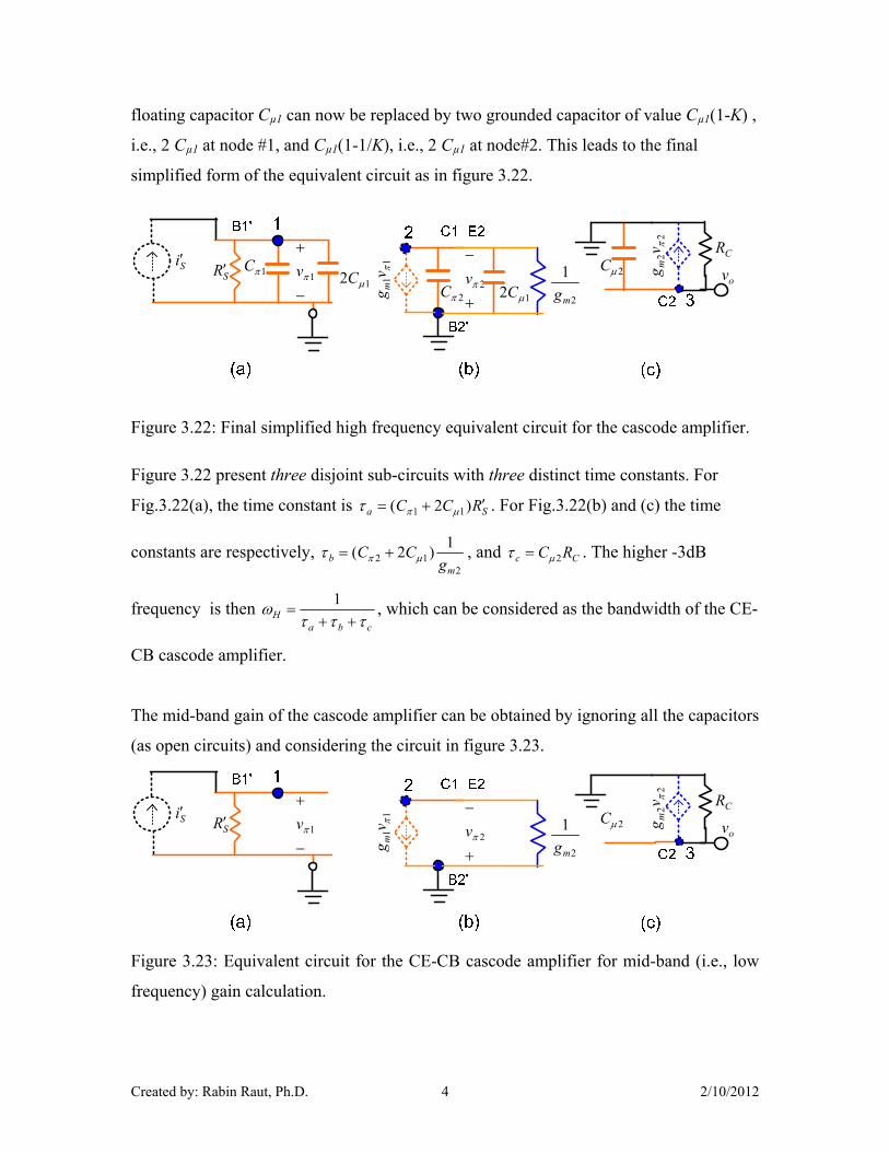
Created by: Rabin Raut, Ph.D. 4 2/10/2012
floating capacitor Cµ1 can now be replaced by two grounded capacitor of value Cµ1(1-K) ,
i.e., 2 Cµ1 at node #1, and Cµ1(1-1/K), i.e., 2 Cµ1 at node#2. This leads to the final
simplified form of the equivalent circuit as in figure 3.22.
SR 1C12 C
1vSi
2v2C
11
vg m 2
1
mg12 C
2C
22
vg m
CR
ov
Figure 3.22: Final simplified high frequency equivalent circuit for the cascode amplifier.
Figure 3.22 present three disjoint sub-circuits with three distinct time constants. For
Fig.3.22(a), the time constant is Sa RCC )2( 11 . For Fig.3.22(b) and (c) the time
constants are respectively, 2
121
)2(m
b gCC , and Cc RC 2 . The higher -3dB
frequency is then cba
H
1, which can be considered as the bandwidth of the CE-
CB cascode amplifier.
The mid-band gain of the cascode amplifier can be obtained by ignoring all the capacitors
(as open circuits) and considering the circuit in figure 3.23.
SR
1vSi
2v
11
vg m 2
1
mg
2C
22
vg m
CR
ov
Figure 3.23: Equivalent circuit for the CE-CB cascode amplifier for mid-band (i.e., low
frequency) gain calculation.
Created by: Rabin Raut, Ph.D. 5 2/10/2012
By inspection, 12
12 )1
(Xsig
sS
mmCmo rR
vR
ggRgv
= s
XsigCm v
rrR
rRg
11
11
(3.33)
The mid-band gain is then CXsig
mMs
o RrrR
rgA
v
v
11
11
(3.34)
Exercise 3.6.1.1.1:Consider an NPN BJT device with hFE=100, fT=6000 MHz, Cπ= 25 pF
biased to operate at IE= 1 mA. Given that rX=10 Ω, VA =50 V, and the signal source
resistance Rsig =100 Ω. The load resistance RC is 2.7 kΩ.
(a)The BJT is used as a CE amplifier with above given parameters. Find the mid-band
gain AM , the upper cut-off frequency f-3dB, and hence the Gain-Bandwidth (GBW) of the
amplifier (note: GBW=AM times f-3dB)
(b)Two matched BJT devices with above specifications are used to construct a CE-CB
cascode amplifier. Find the mid-band gain AM , the upper cut-off frequency f-3dB, and
hence the Gain-Bandwidth (GBW) of the amplifier (note: GBW=AM times f-3dB).
(c)How does the GBW|CE compare with the GBW|Cascode ?
(Hint: the student need to first determine gm, rπ, ro, and Cµ for the BJT from the given
information)
Example 3.6.1.1.2: On using a typical BJT devices from SPICE simulation library, we get
the following results:
Amplifier mode CE CB CE-CB cascode
Gain 61.1 15.1 63.8
Band width 180.1MHz 793.5MHz 616.2MHz
3.6.2 CS-CG MOSFET cascode amplifier
It is easy to construct a cascode of CS-CG amplifier stages using MOSFET devices. The
schematic and the high frequency equivalent circuit are shown in figures 3.24(a)-(b)
respectively. I should be noted that the source terminals of transistors M1,M2 cannot be
connected to the respective body (substrate) terminals and hence the associated parasitic
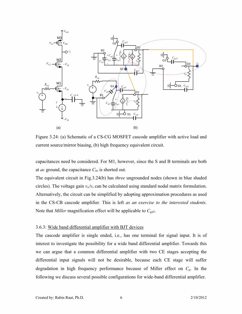
Created by: Rabin Raut, Ph.D. 6 2/10/2012
DDV
SSV
C
I
SSV
SSV
M1
M22GV
D1
1gsv 1or
11
gsm
vgB1
G1
S1
1gbC1gdC
1gsC
1bdC
+-
sv
sigR+-
sv
sigR
M3
3GV DDV
ovD2
2gsv
2bsv2or
22
sm
vg
22
sm
bv
gB2
G2 2gdC
2gsC
2bsC
2bdCS2
D3
3or
G3
S3
3gdC
3bdC
B3ov
(a) (b)
Figure 3.24: (a) Schematic of a CS-CG MOSFET cascode amplifier with active load and
current source/mirror biasing, (b) high frequency equivalent circuit.
capacitances need be considered. For M1, however, since the S and B terminals are both
at ac ground, the capacitance Cbs is shorted out.
The equivalent circuit in Fig.3.24(b) has three ungrounded nodes (shown in blue shaded
circles). The voltage gain vo/vs can be calculated using standard nodal matrix formulation.
Alternatively, the circuit can be simplified by adopting approximation procedures as used
in the CS-CB cascode amplifier. This is left as an exercise to the interested students.
Note that Miller magnification effect will be applicable to Cgd1.
3.6.3: Wide band differential amplifier with BJT devices
The cascode amplifier is single ended, i.e., has one terminal for signal input. It is of
interest to investigate the possibility for a wide band differential amplifier. Towards this
we can argue that a common differential amplifier with two CE stages accepting the
differential input signals will not be desirable, because each CE stage will suffer
degradation in high frequency performance because of Miller effect on C. In the
following we discuss several possible configurations for wide-band differential amplifier.
Created by: Rabin Raut, Ph.D. 7 2/10/2012
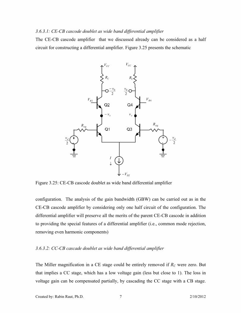
3.6.3.1: CE-CB cascode doublet as wide band differential amplifier
The CE-CB cascode amplifier that we discussed already can be considered as a half
circuit for constructing a differential amplifier. Figure 3.25 presents the schematic
EEV
2BV
CR
CCV
20v
xv
sigR
2dv
sigR
2dv
xv
20v
CR
I
CCV
4BV
Figure 3.25: CE-CB cascode doublet as wide band differential amplifier
configuration. The analysis of the gain bandwidth (GBW) can be carried out as in the
CE-CB cascode amplifier by considering only one half circuit of the configuration. The
differential amplifier will preserve all the merits of the parent CE-CB cascode in addition
to providing the special features of a differential amplifier (i.e., common mode rejection,
removing even harmonic components)
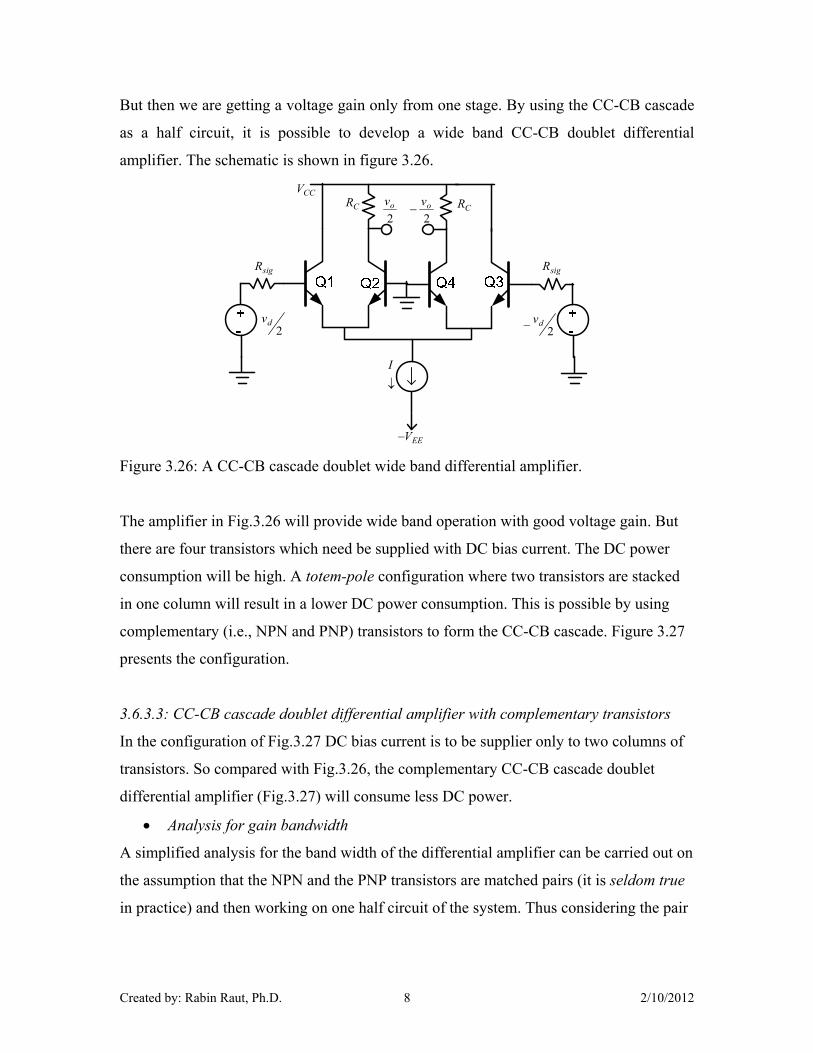
3.6.3.2: CC-CB cascade doublet as wide band differential amplifier
The Miller magnification in a CE stage could be entirely removed if RC were zero. But
that implies a CC stage, which has a low voltage gain (less but close to 1). The loss in
voltage gain can be compensated partially, by cascading the CC stage with a CB stage.
Created by: Rabin Raut, Ph.D. 8 2/10/2012
But then we are getting a voltage gain only from one stage. By using the CC-CB cascade
as a half circuit, it is possible to develop a wide band CC-CB doublet differential
amplifier. The schematic is shown in figure 3.26.
EEV
CCV
I
CR CR
2dv
2dv
sigR sigR
2ov
2ov
Figure 3.26: A CC-CB cascade doublet wide band differential amplifier.
The amplifier in Fig.3.26 will provide wide band operation with good voltage gain. But
there are four transistors which need be supplied with DC bias current. The DC power
consumption will be high. A totem-pole configuration where two transistors are stacked
in one column will result in a lower DC power consumption. This is possible by using
complementary (i.e., NPN and PNP) transistors to form the CC-CB cascade. Figure 3.27
presents the configuration.
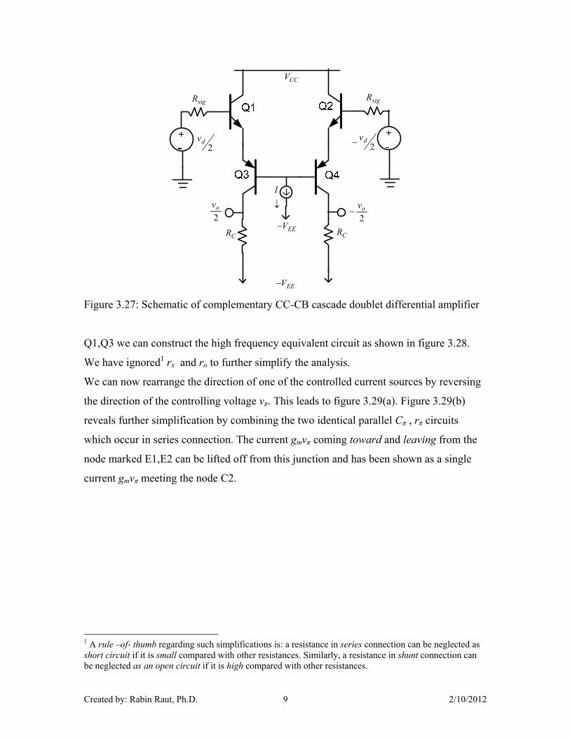
3.6.3.3: CC-CB cascade doublet differential amplifier with complementary transistors
In the configuration of Fig.3.27 DC bias current is to be supplier only to two columns of
transistors. So compared with Fig.3.26, the complementary CC-CB cascade doublet
differential amplifier (Fig.3.27) will consume less DC power.
Analysis for gain bandwidth
A simplified analysis for the band width of the differential amplifier can be carried out on
the assumption that the NPN and the PNP transistors are matched pairs (it is seldom true
in practice) and then working on one half circuit of the system. Thus considering the pair
Created by: Rabin Raut, Ph.D. 9 2/10/2012
EEV
CCV
2dv
sigR
CR
2ov
2dv
sigR
CR
2ov
EEV
I
Figure 3.27: Schematic of complementary CC-CB cascade doublet differential amplifier
Q1,Q3 we can construct the high frequency equivalent circuit as shown in figure 3.28.
We have ignored1 rx and ro to further simplify the analysis.
We can now rearrange the direction of one of the controlled current sources by reversing
the direction of the controlling voltage vπ. This leads to figure 3.29(a). Figure 3.29(b)
reveals further simplification by combining the two identical parallel Cπ , rπ circuits
which occur in series connection. The current gmvπ coming toward and leaving from the
node marked E1,E2 can be lifted off from this junction and has been shown as a single
current gmvπ meeting the node C2.
1 A rule –of- thumb regarding such simplifications is: a resistance in series connection can be neglected as short circuit if it is small compared with other resistances. Similarly, a resistance in shunt connection can be neglected as an open circuit if it is high compared with other resistances.
Created by: Rabin Raut, Ph.D. 10 2/10/2012
r C C vg m
v
rCC v
gm
v
2dv
sigR
CR2ov
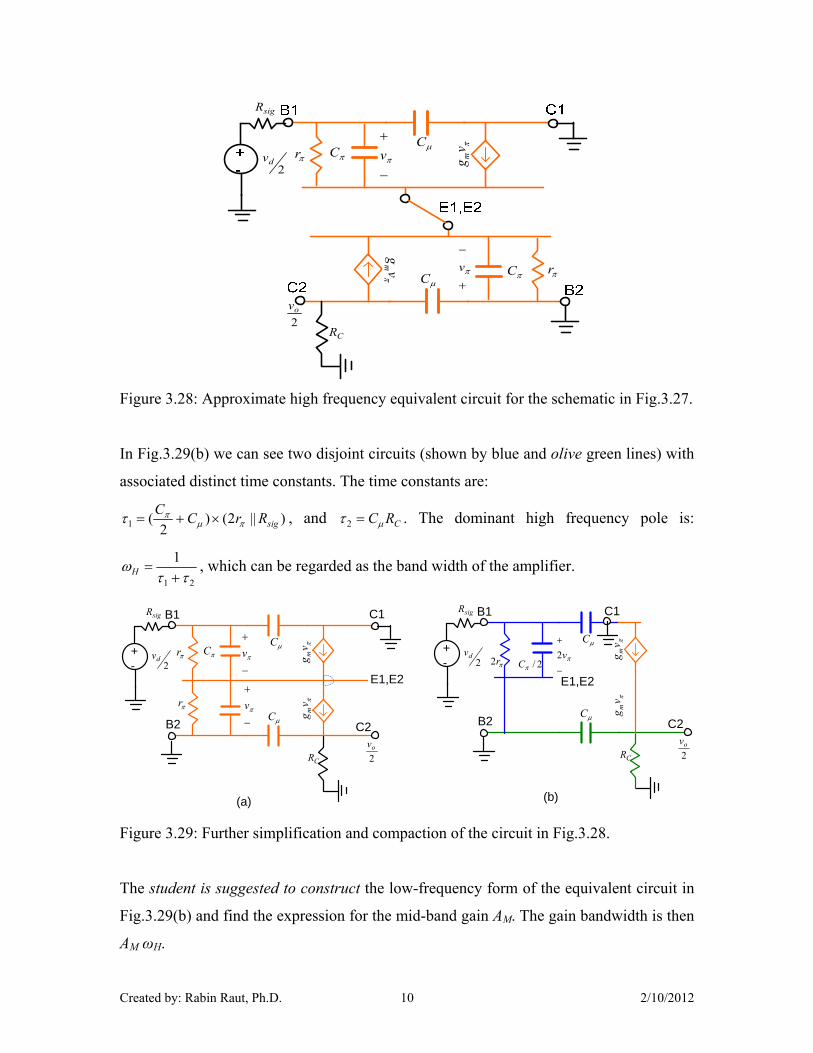
Figure 3.28: Approximate high frequency equivalent circuit for the schematic in Fig.3.27.
In Fig.3.29(b) we can see two disjoint circuits (shown by blue and olive green lines) with
associated distinct time constants. The time constants are:
)||2()2
(1 sigRrCC
, and CRC 2 . The dominant high frequency pole is:
21
1
H , which can be regarded as the band width of the amplifier.
B1 C1 B1 C1
+- 2
dv
sigR
r C C vg
m
v+- 2
dv
sigR
E1,E2
B2 C2
CR 2ov
vg
m
vC
r
r2 2/C
C vg
m
v2
E1,E2
B2 C2
CR 2ov
vg
m
C
(a) (b)
Figure 3.29: Further simplification and compaction of the circuit in Fig.3.28.
The student is suggested to construct the low-frequency form of the equivalent circuit in
Fig.3.29(b) and find the expression for the mid-band gain AM. The gain bandwidth is then
AM ωH.
Created by: Rabin Raut, Ph.D. 11 2/10/2012
3.6.4:Wide band amplifiers with MOSFET transistors
Enhancement mode MOSFET can be connected in the same way as BJT stages to derive
cascode and wide band differential amplifiers for high frequency applications. The
analysis follows similarly.
The student is encouraged to draw the schematics with MOSFET devices by following the
corresponding BJT configurations in sections 3.6.3.1-3.
3.7: Practice Exercises
3.7.1: Show by appropriate analysis (KCL/KVL/Nodal matrix) that the voltage signal
coupled across the internal base-emitter junction of a BJT (i.e., vπ) has a (a) zero at ω=0,
when a voltage source signal is fed to the base of the BJT via a series capacitor, and (b)
has a zero at a finite frequency when parallel R,C network is in series with the voltage
source. Use the low-frequency equivalent circuit for the transistor. Consider the
representative cases as shown below.
3.7.2: For the BJT CE amplifier below, given RS=600 ohms, RB= 22 k ohms, hfe=99, IC=2
mA, RE= 1.5 k ohms, RC=2.2 k ohms, RL=1 k ohms, C1 =1 μF, C2=25 μF, C3= 10 μF.
What will be the lower -3dB frequency for the amplifier?
Created by: Rabin Raut, Ph.D. 12 2/10/2012
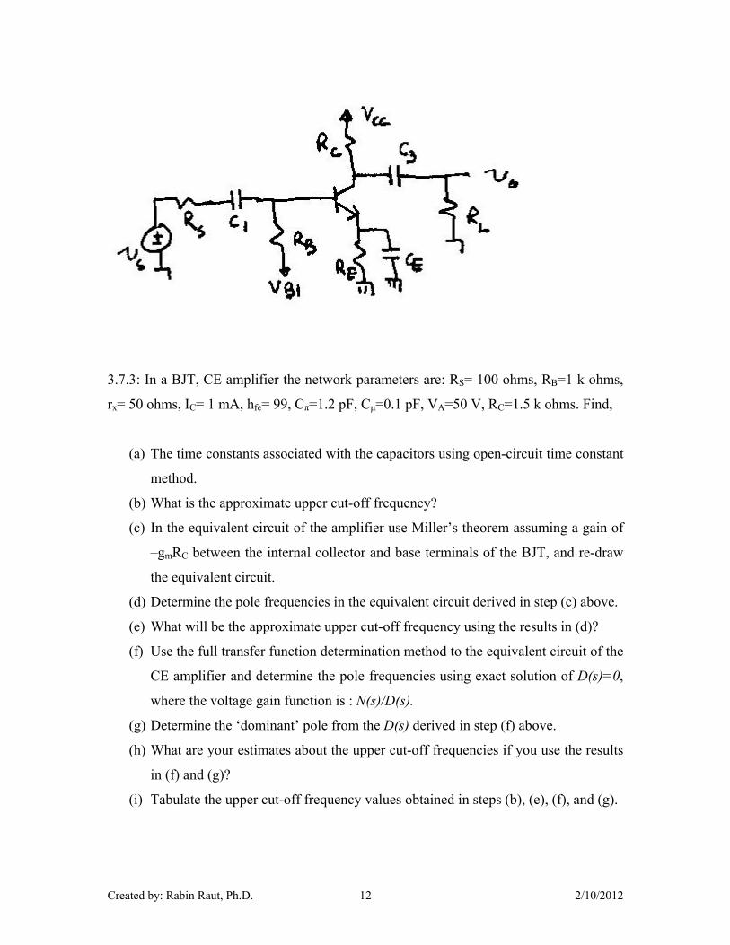
3.7.3: In a BJT, CE amplifier the network parameters are: RS= 100 ohms, RB=1 k ohms,
rx= 50 ohms, IC= 1 mA, hfe= 99, Cπ=1.2 pF, Cμ=0.1 pF, VA=50 V, RC=1.5 k ohms. Find,
(a) The time constants associated with the capacitors using open-circuit time constant
method.
(b) What is the approximate upper cut-off frequency?
(c) In the equivalent circuit of the amplifier use Miller’s theorem assuming a gain of
–gmRC between the internal collector and base terminals of the BJT, and re-draw
the equivalent circuit.
(d) Determine the pole frequencies in the equivalent circuit derived in step (c) above.
(e) What will be the approximate upper cut-off frequency using the results in (d)?
(f) Use the full transfer function determination method to the equivalent circuit of the
CE amplifier and determine the pole frequencies using exact solution of D(s)=0,
where the voltage gain function is : N(s)/D(s).
(g) Determine the ‘dominant’ pole from the D(s) derived in step (f) above.
(h) What are your estimates about the upper cut-off frequencies if you use the results
in (f) and (g)?
(i) Tabulate the upper cut-off frequency values obtained in steps (b), (e), (f), and (g).
Created by: Rabin Raut, Ph.D. 13 2/10/2012
3.7.4: In a MOSFET amplifier, you are given the following: RS=100 ohms, Cgs=0.1 pF,
Cgd=20 fF, gm =50 μ mho, IDC=50 μA, VA=20 V, and RL= 5 k ohms. The MOSFET
amplifier is configured to operate as CS amplifier. Find the dominant high-frequency
pole of the amplifier using:
(a) Miller’s theorem
(b) Full nodal analysis
(c) Open-circuit time constant method
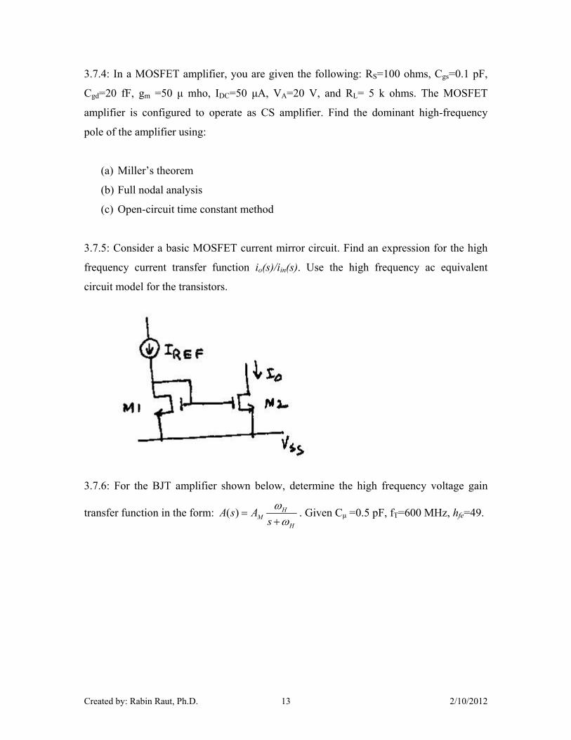
3.7.5: Consider a basic MOSFET current mirror circuit. Find an expression for the high
frequency current transfer function io(s)/iin(s). Use the high frequency ac equivalent
circuit model for the transistors.
3.7.6: For the BJT amplifier shown below, determine the high frequency voltage gain
transfer function in the form: ( ) HM
H
A s As
. Given Cμ =0.5 pF, fT=600 MHz, hfe=49.
Created by: Rabin Raut, Ph.D. 14 2/10/2012
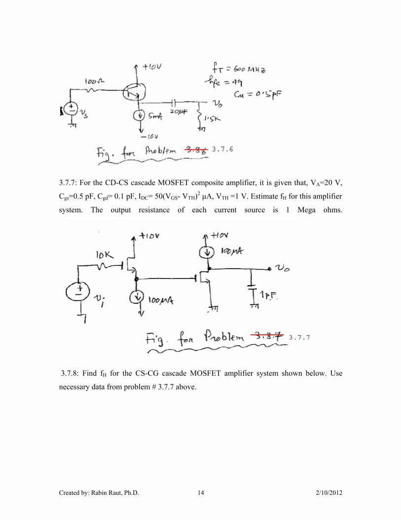
3.7.7: For the CD-CS cascade MOSFET composite amplifier, it is given that, VA=20 V,
Cgs=0.5 pF, Cgd= 0.1 pF, IDC= 50(VGS- VTH)2 μA, VTH =1 V. Estimate fH for this amplifier
system. The output resistance of each current source is 1 Mega ohms.
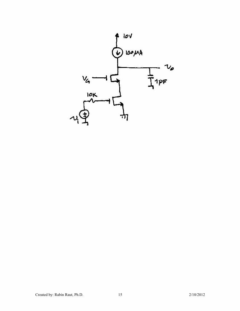
3.7.8: Find fH for the CS-CG cascade MOSFET amplifier system shown below. Use
necessary data from problem # 3.7.7 above.
Created by: Rabin Raut, Ph.D. 15 2/10/2012