Metal Oxide Semiconductor Field Effect Transistor …ee.sc.edu/personal/faculty/simin/ELCT563/15...
25
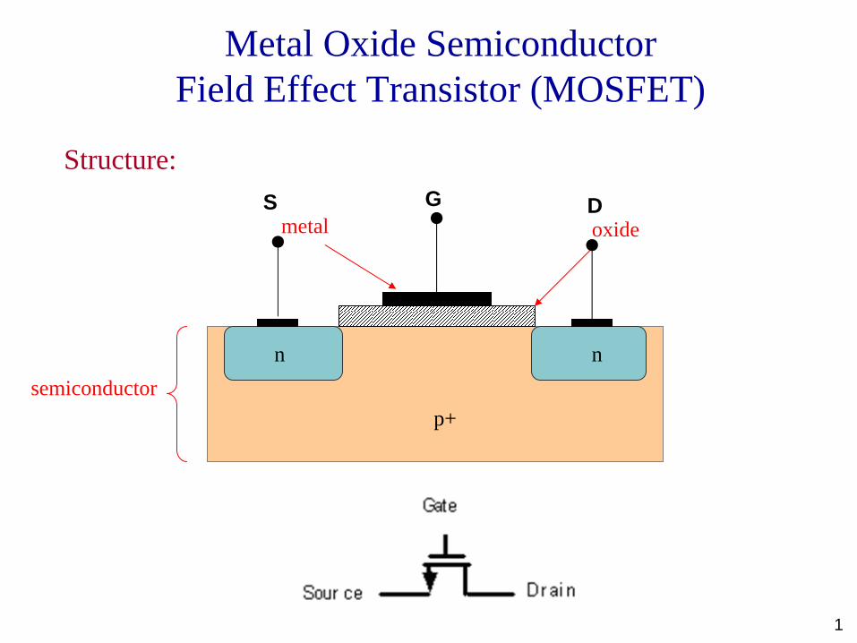
1 Metal Oxide Semiconductor Field Effect Transistor (MOSFET) Structure: metal oxide semiconductor p+ n n S G D
Transcript of Metal Oxide Semiconductor Field Effect Transistor …ee.sc.edu/personal/faculty/simin/ELCT563/15...
1
Metal Oxide Semiconductor Field Effect Transistor (MOSFET)
Structure:
metal oxide
semiconductorp+
n n
S G D
2
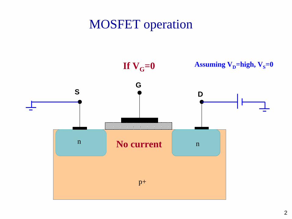
MOSFET operation
p+
n n
SG
D
If VG=0
n
Assuming VD=high, VS=0
No current
3
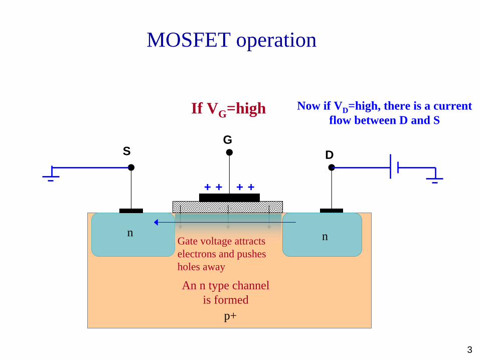
p+
n n
SG
D
If VG=high
n
+ + + +
An n type channel is formed
Now if VD=high, there is a current flow between D and S
Gate voltage attracts electrons and pushes holes away
MOSFET operation
4
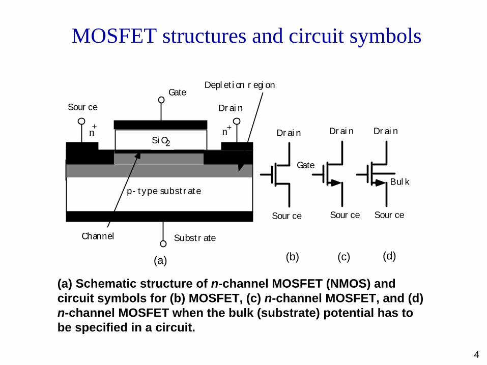
MOSFET structures and circuit symbols
p- type subst r ate
Sour ce Dr ai n
Gate
Subst r ate
Si O2Dr ai n
Sour ce Sour ce
Dr ai n
Gate
Sour ce
Dr ai n
Bul k
Channel
Depl et i on r egi on
n+ n+
(a) (b) (d)(c)
(a) Schematic structure of n-channel MOSFET (NMOS) and circuit symbols for (b) MOSFET, (c) n-channel MOSFET, and (d) n-channel MOSFET when the bulk (substrate) potential has to be specified in a circuit.
5
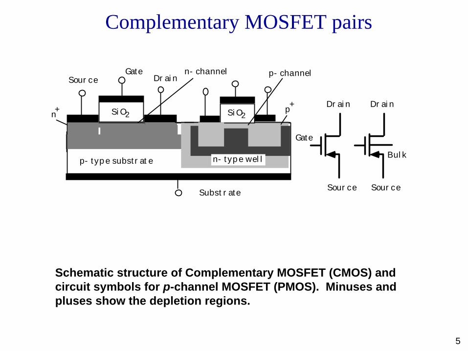
Complementary MOSFET pairs
Schematic structure of Complementary MOSFET (CMOS) and circuit symbols for p-channel MOSFET (PMOS). Minuses and pluses show the depletion regions.
p- typ e subst r at e
n+
Sour ce Dr ai nGate
Subst r ate
Si O2
Sour ce
Dr ai n
Gate
Sour ce
Dr ai n
Bul k
p+
n- channel p- channel
n- typ e wel l
Si O2
6
Sub-threshold mode of MOSFET operation
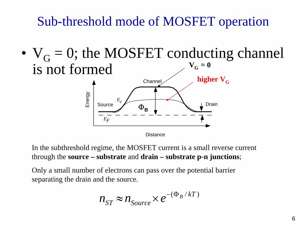
• VG = 0; the MOSFET conducting channel is not formed
Ec
EF
²E F1²E F2
Channel
Source DrainEne
rgy
Distance
In the subthreshold regime, the MOSFET current is a small reverse current through the source – substrate and drain – substrate p-n junctions;
Only a small number of electrons can pass over the potential barrier separating the drain and the source.
VG = 0
higher VG
ΦB
( / )B kTST Sourcen n e− Φ≈ ×
7
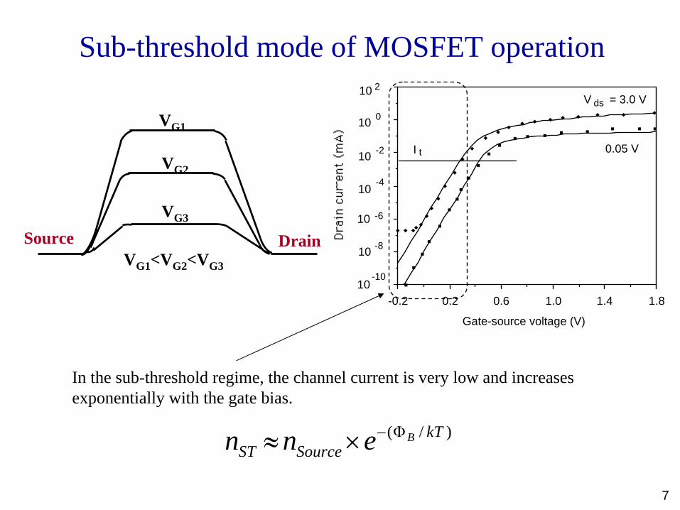
In the sub-threshold regime, the channel current is very low and increases exponentially with the gate bias.
DrainSource
VG1
VG2
VG3
VG1<VG2<VG3
Gate-source voltage (V)
1.81.41.00.60.2-0.2
0
-10
-8
-6
10 2
-4
-2 0.05 V
V ds = 3.0 V
I t10
10
10
10
10
10
Sub-threshold mode of MOSFET operation
( / )B kTST Sourcen n e− Φ≈ ×
8
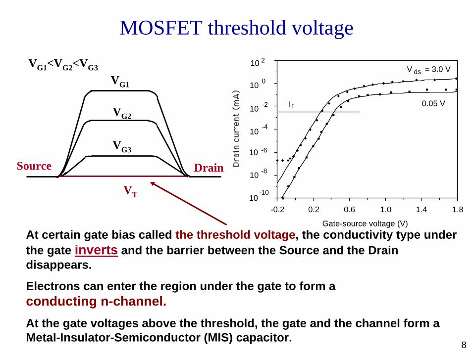
At certain gate bias called the threshold voltage, the conductivity type under the gate inverts and the barrier between the Source and the Drain disappears.
Electrons can enter the region under the gate to form a conducting n-channel.At the gate voltages above the threshold, the gate and the channel form a Metal-Insulator-Semiconductor (MIS) capacitor.
DrainSource
VG1
VG2
VG3
VG1<VG2<VG3
Gate-source voltage (V)
1.81.41.00.60.2-0.2
0
-10
-8
-6
10 2
-4
-2 0.05 V
V ds = 3.0 V
I t10
10
10
10
10
10
MOSFET threshold voltage
VT
9
The free electron charge in the MOSFET channel (per unit area):
Q1 = CGATE × (VG – VT)(assuming that at VG = VT the free electron concentration is zero)
MOSFET above the threshold voltage
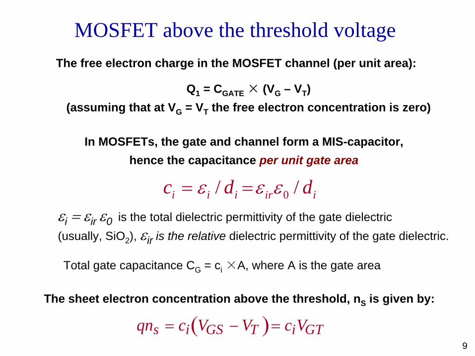
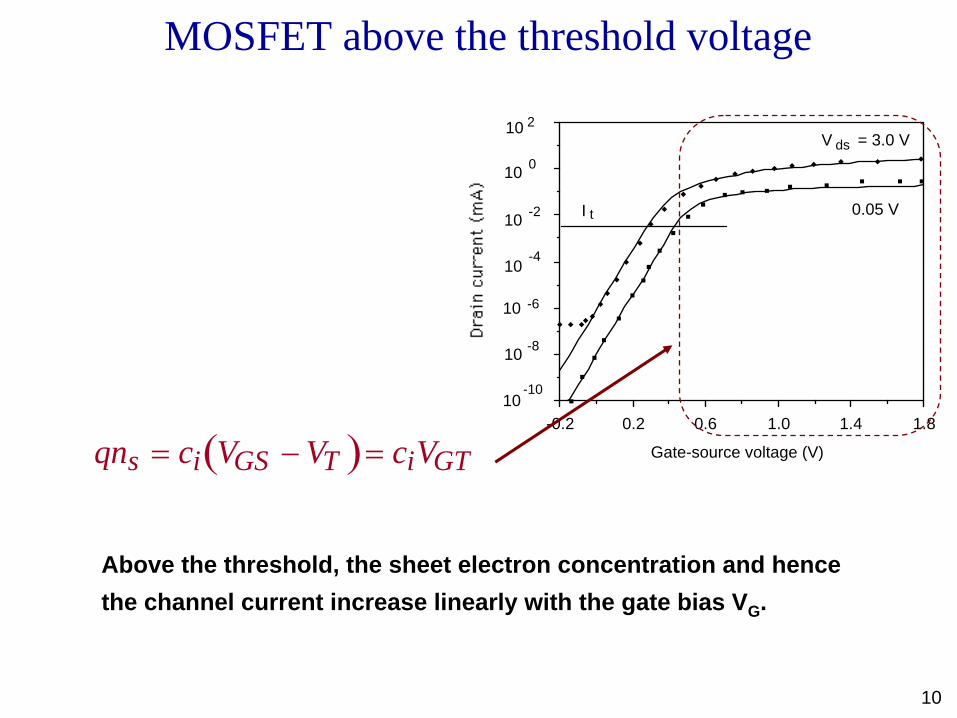
qns = ci VGS − VT( )= ciVGT
0/ /i i i ir ic d dε ε ε= =
The sheet electron concentration above the threshold, nS is given by:
In MOSFETs, the gate and channel form a MIS-capacitor, hence the capacitance per unit gate area
εi = εir ε0 is the total dielectric permittivity of the gate dielectric (usually, SiO2), εir is the relative dielectric permittivity of the gate dielectric.
Total gate capacitance CG = ci ×A, where A is the gate area
10
Above the threshold, the sheet electron concentration and hence the channel current increase linearly with the gate bias VG.
Gate-source voltage (V)
1.81.41.00.60.2-0.2
0
-10
-8
-6
10 2
-4
-2 0.05 V
V ds = 3.0 V
I t10
10
10
10
10
10
MOSFET above the threshold voltage
qns = ci VGS − VT( )= ciVGT

11
MOSFET Threshold Voltage
semiconductor
metal oxide
p+
n n
S G D
DrainSource
12
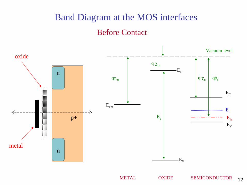
Band Diagram at the MOS interfaces
metal
oxide
p+
n
n
Before Contact
EC
EV
EFs
Ei
Vacuum level
OXIDEMETAL SEMICONDUCTOR
EFm
EC
EV
qφm
Eg
q χox
q χsq χs qφs
13
p+
n
n
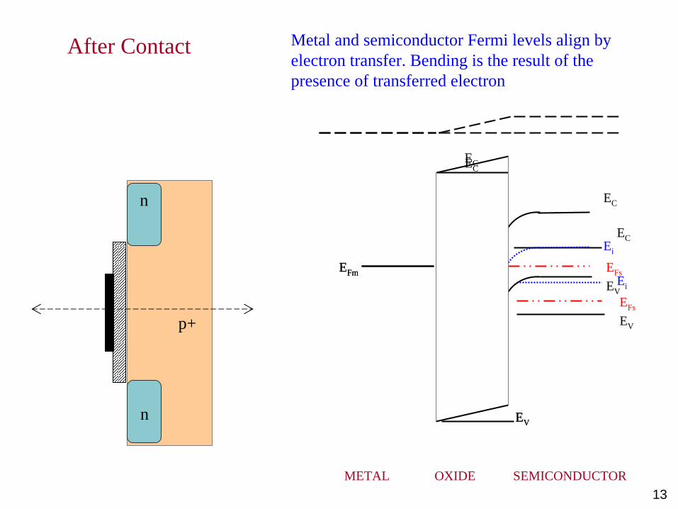
After Contact
OXIDEMETAL SEMICONDUCTOR
EC
EV
EFs
Ei
EFm
EC
EV
EC
EV
EFs
Ei
EFm
EC
EV
Metal and semiconductor Fermi levels align by electron transfer. Bending is the result of the presence of transferred electron
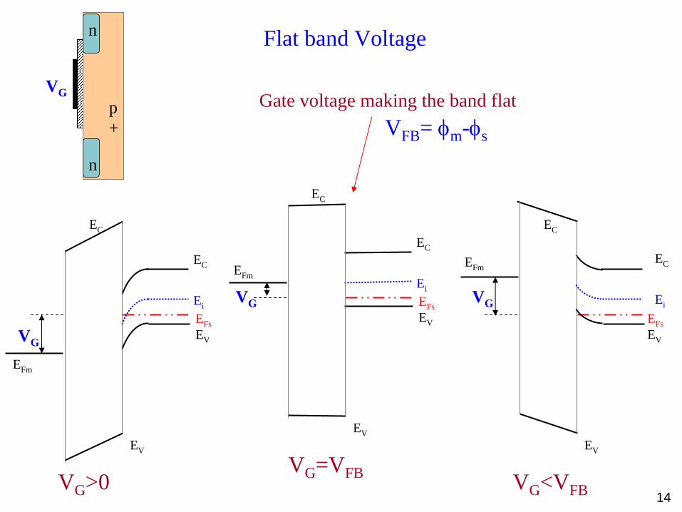
14VG>0
p+
n
n
VG
EC
EV
EFs
Ei
EFm
EC
EV
VG
VG<VFB
EC
EV
EFs
Ei
EFm
EC
EV
VG
VG=VFB
EC
EV
EFs
Ei
EFm
EC
EV
VG
Flat band Voltage
Gate voltage making the band flatVFB= φm-φs
15
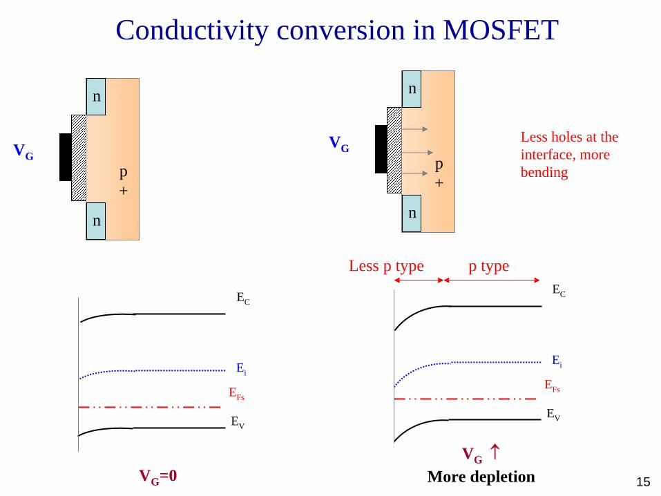
Conductivity conversion in MOSFET
EC
EV
EFs
Ei
VG=0
p+
VG
n
n
EC
EV
EFs
Ei
VG ↑
p+
VG
n
n
Less holes at the interface, more bending
p typeLess p type
More depletion
16
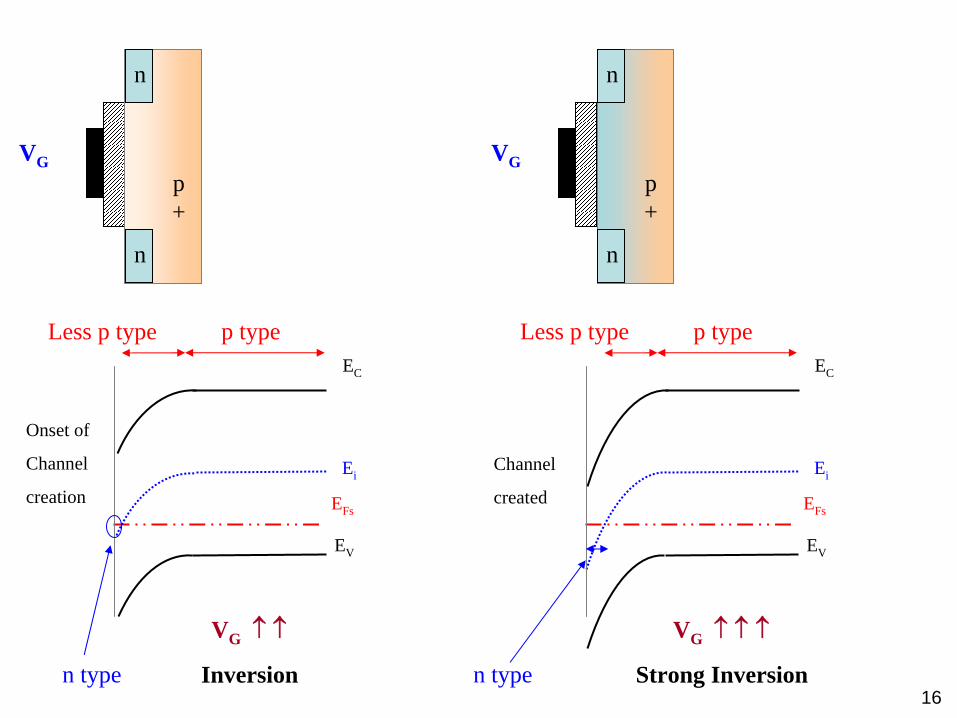
EC
EV
EFs
Ei
VG ↑ ↑
p+
VG
n
n
p typeLess p type
n type Inversion
EC
EV
EFs
Ei
VG ↑ ↑ ↑
p+
VG
n
n
p typeLess p type
n type Strong Inversion
Onset of
Channel
creation
Channel
created
17
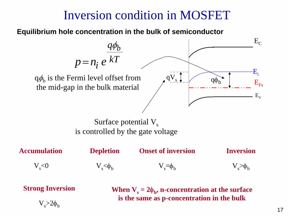
Inversion condition in MOSFET
EC
EV
EFs
Eiqφb
qVs
Surface potential Vsis controlled by the gate voltage
Accumulation
Vs<0
Depletion
Vs<φb
Onset of inversion
Vs=φb
Inversion
Vs>φb
Strong Inversion
Vs>2φb
bqkTip n eφ
=
Equilibrium hole concentration in the bulk of semiconductor
qφb is the Fermi level offset from the mid-gap in the bulk material
When Vs = 2φb, n-concentration at the surface is the same as p-concentration in the bulk
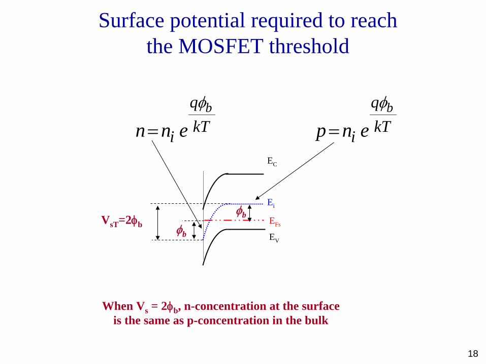
18
Surface potential required to reach the MOSFET threshold
When Vs = 2φb, n-concentration at the surface is the same as p-concentration in the bulk
bqkTip n eφ
=EC
EV
EFs
Ei
VsT=2φbφb
φb
bqkTin n eφ
=
19
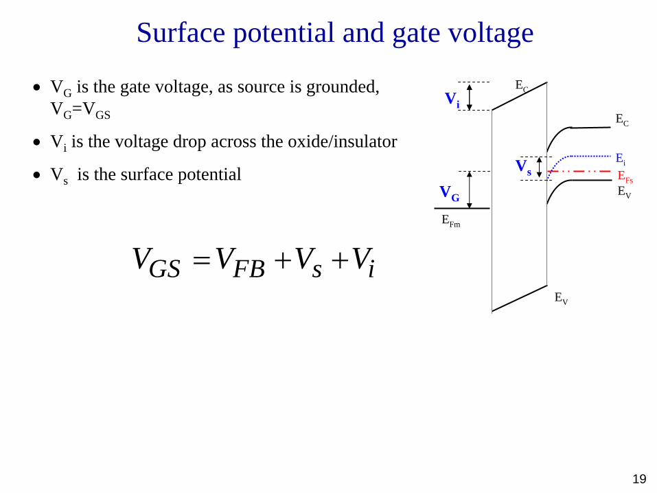
Surface potential and gate voltage
EC
EV
EFs
Ei
EFm
EC
EV
VG
Vi
Vs
• VG is the gate voltage, as source is grounded, VG=VGS
• Vi is the voltage drop across the oxide/insulator
• Vs is the surface potential
GS FB s iV V V V= + +
20
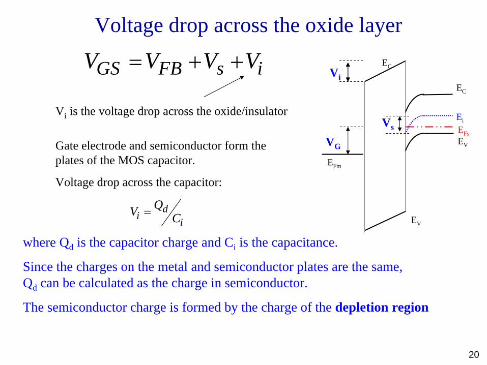
Voltage drop across the oxide layer
EC
EV
EFs
Ei
EFm
EC
EV
VG
Vi
Vs
Vi is the voltage drop across the oxide/insulator
GS FB s iV V V V= + +
di iQV C=
where Qd is the capacitor charge and Ci is the capacitance.
Since the charges on the metal and semiconductor plates are the same, Qd can be calculated as the charge in semiconductor.
The semiconductor charge is formed by the charge of the depletion region
Gate electrode and semiconductor form the plates of the MOS capacitor.
Voltage drop across the capacitor:
21
Voltage drop across the oxide layer
EC
EV
EFs
Ei
EFm
EC
EV
VG
Vi
Vs
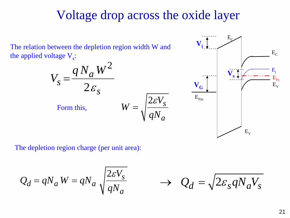
The relation between the depletion region width W and the applied voltage Vs:
2d s a sQ qN Vε→ =
2
2a
ss
q N WV
ε=
2 s
a
VW
qNε
=Form this,
2 sd a a
a
VQ qN W qN
qNε
= =
The depletion region charge (per unit area):
22
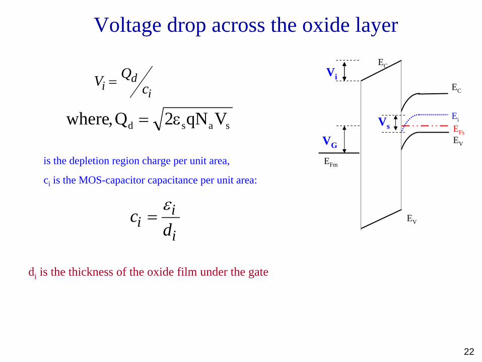
Voltage drop across the oxide layer
EC
EV
EFs
Ei
EFm
EC
EV
VG
Vi
Vs
di iQV c=
is the depletion region charge per unit area,
ci is the MOS-capacitor capacitance per unit area:
sasd VqN2Q,where ε=
di is the thickness of the oxide film under the gate
ii
ic
dε
=
23
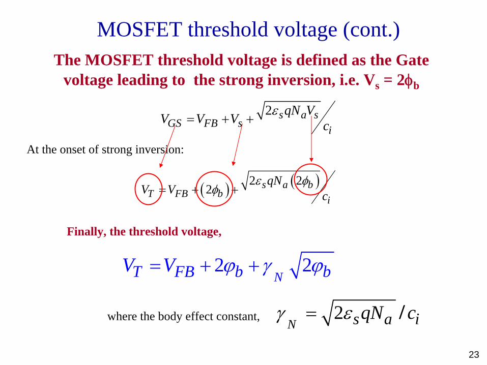
MOSFET threshold voltage (cont.)
2 s a sGS FB s i
qN VV V V cε
= + +
At the onset of strong inversion:
( ) ( )2 22 s a b
T FB b i
qNV V c
ε φφ= + +
2 2NT FB b bV V ϕ γ ϕ= + +
Finally, the threshold voltage,
2N s a iqN c/γ ε=where the body effect constant,
The MOSFET threshold voltage is defined as the Gate voltage leading to the strong inversion, i.e. Vs = 2φb

24
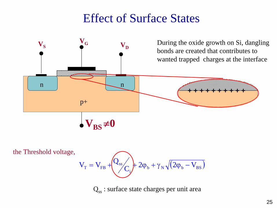
Effect of Body Bias
p+
n n
VSVG VD
VBS ≠0
( )BSbNbFBT V22VV −ϕγ+ϕ+=
the Threshold voltage,
25
Effect of Surface States
p+
n n
VSVG VD
VBS ≠0
( )BSbNbi
ssFBT V22C
QVV −ϕγ+ϕ++=
the Threshold voltage,
During the oxide growth on Si, dangling bonds are created that contributes to wanted trapped charges at the interface
+ + + + + + + + + +
Qss : surface state charges per unit area