M82510 ASYNCHRONOUS SERIAL CONTROLLER - slot …slot-tech.com/interesting_stuff/Data Sheets/Other...
40
*Other brands and names are the property of their respective owners. Information in this document is provided in connection with Intel products. Intel assumes no liability whatsoever, including infringement of any patent or copyright, for sale and use of Intel products except as provided in Intel’s Terms and Conditions of Sale for such products. Intel retains the right to make changes to these specifications at any time, without notice. Microcomputer Products may have minor variations to this specification known as errata. March 1996 COPYRIGHT ' INTEL CORPORATION, 1996 Order Number: 271072-007 M82510 ASYNCHRONOUS SERIAL CONTROLLER Military Y Asynchronous Operation — 5- to 9-Bit Character Format — Baud Rate DC to 288k — Complete Error Detection Y Multiple Sampling Windows Y Two, Independent, Four-Byte Transmit and Receive FIFOs — Programmable Threshold Y Two, 16-bit Baud Rate Generators/ Timers Y System Clock Options — On-Chip Crystal Oscillator — External Clocks Y MCS-51 9-Bit Protocol Support Y Control Character Recognition Y CHMOS III with Power Down Mode Y Interrupts Maskable at Two Levels Y Auto Echo and Loopback Modes Y Seven I/O Pins, Dedicated and General Purpose Y Available in 28-Lead CERDIP and 28-Pad LCC Packages Y Military Temperature Range: b 55§ C to a 125§ C (T C ) The Intel CHMOS M82510 is designed to increase system efficiency in asynchronous environments such as modems, serial ports—including expanding performance areas: MCS-51 9-bit format and high speed async. The functional support provided in the M82510 is unparalleled—2 baud rate generators/timers provide inde- pendent data rates or protocol timeouts; a crystal oscillator and smart modem I/O simplify system logic. New features, dual FIFOs and Control Character Recognition (CCR), dramatically reduce CPU interrupts and in- crease software efficiency. The M82510’s software versatility allows emulation of the INS 8250A/16450 for IBM PC AT* compatibility or a high performance mode, configured by 35 control registers. All interrupts are maskable at 2 levels. The multi-personality I/O pins are configurable as desired. A DPLL and multiple sampling of serial data improve data reliability for high speed asynchronous communication. The compact 28-pin M82510 is fabricated in CHMOS III technology and includes a software powerdown option. *IBM and PC AT are registered trademarks of IBM Corporation. 271072–1 Figure 1. Block Diagram
-
Upload
hoangxuyen -
Category
Documents
-
view
222 -
download
1
Transcript of M82510 ASYNCHRONOUS SERIAL CONTROLLER - slot …slot-tech.com/interesting_stuff/Data Sheets/Other...

*Other brands and names are the property of their respective owners.Information in this document is provided in connection with Intel products. Intel assumes no liability whatsoever, including infringement of any patent orcopyright, for sale and use of Intel products except as provided in Intel’s Terms and Conditions of Sale for such products. Intel retains the right to makechanges to these specifications at any time, without notice. Microcomputer Products may have minor variations to this specification known as errata.
March 1996COPYRIGHT © INTEL CORPORATION, 1996 Order Number: 271072-007
M82510ASYNCHRONOUS SERIAL CONTROLLER
Military
Y Asynchronous OperationÐ 5- to 9-Bit Character FormatÐ Baud Rate DC to 288kÐ Complete Error Detection
Y Multiple Sampling Windows
Y Two, Independent, Four-Byte Transmitand Receive FIFOsÐ Programmable Threshold
Y Two, 16-bit Baud Rate Generators/Timers
Y System Clock OptionsÐ On-Chip Crystal OscillatorÐ External Clocks
Y MCSÉ-51 9-Bit Protocol Support
Y Control Character Recognition
Y CHMOS III with Power Down Mode
Y Interrupts Maskable at Two Levels
Y Auto Echo and Loopback Modes
Y Seven I/O Pins, Dedicated and GeneralPurpose
Y Available in 28-Lead CERDIP and28-Pad LCC Packages
Y Military Temperature Range:b55§C to a125§C (TC)
The Intel CHMOS M82510 is designed to increase system efficiency in asynchronous environments such asmodems, serial portsÐincluding expanding performance areas: MCSÉ-51 9-bit format and high speed async.The functional support provided in the M82510 is unparalleledÐ2 baud rate generators/timers provide inde-pendent data rates or protocol timeouts; a crystal oscillator and smart modem I/O simplify system logic. Newfeatures, dual FIFOs and Control Character Recognition (CCR), dramatically reduce CPU interrupts and in-crease software efficiency. The M82510’s software versatility allows emulation of the INS 8250A/16450 forIBM PC AT* compatibility or a high performance mode, configured by 35 control registers. All interrupts aremaskable at 2 levels. The multi-personality I/O pins are configurable as desired. A DPLL and multiple samplingof serial data improve data reliability for high speed asynchronous communication. The compact 28-pinM82510 is fabricated in CHMOS III technology and includes a software powerdown option.
*IBM and PC AT are registered trademarks of IBM Corporation.
271072–1
Figure 1. Block Diagram

M82510
28-Pad LCC
271072–55
28-Pin Cerdip
271072–2
Figure 2. Package Pinouts
M82510 PINOUT DEFINITION
SymbolPin
Type Name and DescriptionNo.
RESET 17 I RESET: A high on this input pin resets the M82510 to the Default Wake-upmode.
CS 18 I CHIP SELECT: A low on this input pin enables the M82510 and allows read orwrite operations.
A2–A0 24- I ADDRESS PINS: These inputs interface with three bits of the System Address22 Bus to select one of the internal registers for read or write.
D7–D0 4* I/O DATA BUS: Bidirectional, three state, eight-bit Data Bus. These pins allow25 transfer of bytes between the CPU and the M82510.
RD 20 I READ: A low on this input pin allows the CPU to read Data or Status bytes fromthe M82510.
WR 19 I WRITE: A low on this input allows the CPU to write Data or Control bytes to theM82510.
INT 5 O INTERRUPT: A high on this output pin signals an interrupt request to the CPU.The CPU may determine the particular source and cause of the interrupt byreading the M82510 Status registers.
CLK/X1 9 I MULTIFUNCTION: This input pin serves as a source for the internal systemclock. The clock may be asynchronous to the serial clocks and to the processorclock. This pin may be used in one of two modes: CLK Ð in this mode anexternally generated TTL compatible clock should be used to drive this input pin;X1 Ð in this mode the clock is internally generated by an on-chip crystaloscillator. This mode requires a crystal to be connected between this pin (X1)and the X2 pin. (See System Clock Generation.)
OUT2/X2 8 O MULTIFUNCTION: This is a dual function pin which may be configured to one ofthe following functions: OUT2 Ð a general purpose output pin controlled by theCPU, only available when CLK/X1 pin is driven by an externally generated clock;X2 - this pin serves as an output pin for the crystal oscillator.Note : Theconfiguration of the pin is done only during hardware reset. For more detailsrefer to the System Clock Generation.
*Pins 28–25 and Pins 4–1.
2

M82510
M82510 PINOUT DEFINITION (Continued)
SymbolPin
Type Name and DescriptionNo.
TXD 6 O TRANSMIT DATA: Serial data is transmitted via this output pin starting at theLeast Significant bit.
RXD 13 I RECEIVE DATA: Serial data is received on this input pin starting at the LeastSignificant bit.
RI/SCLK 10 I MULTIFUNCTION: This is a dual function pin which can be configured to one ofthe following functions. RI - Ring Indicator - Input, active low. This is a generalpurpose input pin accessible by the CPU. SCLK - This input pin may serve as asource for the internal serial clock(s), RxClk and/or TxClk. See Figure 12, BRGsources and outputs.
DTR/TB 15 O MULTIFUNCTION: This is a dual function pin which may be configured to one ofthe following functions. DTR - Data Terminal Ready. Output, active low. This is ageneral purpose output pin controlled by the CPU. TB - This pin outputs theBRGB output signal when configured as either a clock generator or as a timer.When BRGB is configured as a timer this pin outputs a ‘‘timer expired pulse.’’When BRGB is configured as a clock generator it outputs the BRGB outputclock.
DSR/TA/ 11 I/O MULTIFUNCTION: This is a multifunction pin which may be configured to one ofthe following functions. DSR - Data Set Ready. Input, active low. This is aOUT0general purpose input pin accessible by the CPU. TA - This pin is similar infunction to pin TB except it outputs the signals from BRGA instead of BRGB.OUT0 - Output pin. This is a general purpose output pin controlled by the CPU.
RTS 16 O REQUEST TO SEND: Output pin, active low. This is a general purpose outputpin controlled by the CPU. In addition, in automatic transmission mode this pin,along with CTS, controls the transmission of data. (See Transmit modes forfurther detail.) During hardware reset this pin is an input. It is used to determinethe System Clock Mode. (See System Clock Generation for further detail.)
CTS 14 I CLEAR TO SEND: Input pin, active low. In automatic transmission mode itdirectly controls the Transmit Machine. (See transmission mode for furtherdetails.) This pin can be used as a General Purpose Input.
DCD/ICLK/ 12 I/O MULTIFUNCTION: This is a multifunction pin which may be configured to one ofthe following functions. DCD - Data Carrier Detected. Input pin, active low. ThisOUT1is a general purpose input pin accessible by the CPU. ICLK - This pin is theoutput of the internal system clock. OUT1 - General purpose output pin.Controlled by the CPU.
VSS 7 P Ground
VCC 21 P Power: a5V Supply
Table 1. Multifunction Pins
Pin Ý I/O Timing Modem
8 *OUT2 X2 Ð
9 Ð *CLK/X1 Ð
10 Ð SCLK *RI
11 OUT0 TA *DSR
12 OUT1 ICLK *DCD
14 Ð Ð *CTS
15 Ð TB *DTR
16 Ð Ð *RTS
*Default
3

M82510
GENERAL DESCRIPTION
The M82510 can be functionally divided into sevenmajor blocks (See Fig 1): Bus Interface Unit, TimingUnit, Modem Module, Tx FIFO, Rx FIFO, Tx Ma-chine, and Rx Machine. Six of these blocks (all ex-cept Bus Interface Unit) can generate block inter-rupts. Three of these blocks can generate second-level interrupts which reflect errors/status within theblock (Receive Machine, Timing Unit, and the Mo-dem Module).
The Bus interface unit allows the M82510 to inter-face with the rest of the system. It controls access todevice registers as well as generation of interruptsto the external world. The FIFOs buffer the CPUfrom the Serial Machines and reduce the interruptoverhead normally required for serial operations.The threshold (level of occupancy in the FIFO whichwill generate an interrupt) is programmable for eachFIFO. The timing unit controls generation of the sys-tem clock through either its on-chip crystal oscillator,or an externally generated clock. It also provides twoBaud Rate Generators/Timers with various optionsand modes to support serial communication.
FUNCTIONAL DESCRIPTION
CPU Interface
The M82510 has a simple demultiplexed Bus Inter-face, which consists of a bidirectional three-stateeight-bit, data bus and a three-bit address bus. AnInterrupt pin along with the Read, Write and ChipSelect are the remaining signals used to interfacewith the CPU. The three address lines along with theBank Pointer register are used to select the regis-ters. The M82510 is designed to interface to all Intelmicroprocessor and microcontroller families. Likemost other I/O based peripherals it is programmedthrough its registers to support a variety of functions.
Its register set can be used in 8250A/16450 com-patibility or High Performance modes. The 8250A/16450 mode is the default wake-up mode in whichonly the 8250A/16450 compatible registers are ac-cessible. The remaining registers are default config-ured to support 8250A/16450 emulation.
Software Interface
271072–3
Figure 3. M82510 Register Architecture
The M82510 is configured and controlled through its35 registers which are divided into four banks. Onlyone bank is accessible at any one time. The bankswitching is done by changing the contents of thebank pointer (GIR/BANK–BANK0, BANK1). Thebanks are logically grouped into 8250A/16450 com-patible (0), General Work Bank (1), General Configu-ration (2), and Modem Configuration (3). The8250A/16450 compatible bank (Bank 0) is the de-fault bank upon power up.
The M82510 registers can be categorized under thefollowing:
Table 2. M82510 Register/Block Functions
Status Enable Configuration Command Data
FIFO FLR Ð FMD Ð Ð
MODEM MSR MIE PMD MCR Ð
RX RST, RXF RIE RMD RCM RXD, RXF
TX LSR LSR TMD TCM TXD, TXF
TIMER TMST TMIE CLCF, TMCR BBL, BBHBACF, BBCF BAL, BAH
DEVICE GSR, GIR GER IMD ICM Ð
8250 LSR, MSR, GIR GER LCR, MCR MCR TXD, RXDBAL, BAH
4

M82510
8250 Compatibility
Upon power up or reset, the M82510 comes up in the default wake up mode. The 8250A/16450 compatiblebank, bank zero, is the accessible bank and all the other registers are configured via their default values tosupport this mode.
Table 3. 8250A/16450 Compatible Registers
M82510 Registers8250A Registers
(Bank 0)
Address Read Write Read Write
00 (DLAB e 0) RxD TxD RBR THR
01 (DLAB e 0) GER GER IER IER
00 (DLAB e 1) BAL BAL DLL DLL
01 (DLAB e 1) BAH BAH DLM DLM
02 GIR/BANK BANK IIR Ð
03 LCR LCR LCR LCR
04 MCR MCR MCR MCR
05 LSR LSR LSR LSR
06 MSR MSR MSR MSR
07 ACR0 ACR0 SCR SCR
Table 4. Default Wake-Up Mode
RxD Ð ACR1 00H RxF Ð
TxD Ð RIE 1EH TxF Ð
BAL 02H RMD 00H TMST 30H
BAH 00H CLCF 00H TMCR Ð
GER 00H BACF 04H FLR 00H
GIR/BANK 01H BBCF 84H RCM Ð
LCR 00H PMD FCH TCM Ð
MCR 00H MIE 0FH GSR 12H
LSR 60H TMIE 00H ICM Ð
MSR 00H BBL 05H FMD 00H
ACR0 00H BBH 00H TMD 00H
RST 00H IMD 0CH
5

M82510
271072–4
Figure 4. Interrupt Structure
Interrupts
There are two levels of interrupt/status reportingwithin the M82510. The first level is the block levelinterrupts such as RX FIFO, Tx FIFO, Rx Machine,Tx Machine, Timing unit, and Modem Module. Thestatus of these blocks is reported in the GeneralStatus and General Interrupt Registers. The secondlevel is the various sources within each block; onlythree of the blocks generate second level interrupts(Rx Machine, Timing Unit, and Modem Module). In-terrupt requests are maskable at both the block leveland at the individual source level within the module.If more than one unmasked block requests interruptservice an on-chip interrupt controller will resolvecontention on a priority basis (each block has a fixedpriority). An interrupt request from a particular blockis activated if one of the unmasked status bits withinthe status register for the block is set. A CPU serviceoperation, e.g., reading the appropriate status regis-ter, will reset the status bits.
ACKNOWLEDGE MODES
The interrupt logic will assert the INT pin when aninterrupt is coded into the General Interrupt register.The INT pin is forced low upon acknowledgment.The M82510 has two modes of interrupt acknowl-edgment:
1. Manual Acknowledge
The CPU must issue an explicit Interrupt Acknowl-edge command via the Interrupt Acknowledge bit ofthe Internal Command register. As a result the INTpin is forced low for two clocks and then updated.
2. Automatic Acknowledge
As opposed to the Manual Acknowledge mode,when the CPU must issue an explicit interrupt ac-knowledge command, an interrupt service operationis considered as an automatic acknowledgment.This forces the INT pin low for two clock cycles.After two cycles the INT pin is updated, i.e., if thereis still an active non-masked interrupt request theINT pin is set HIGH.
INTERRUPT SERVICE
A service operation is an operation performed by theCPU, which causes the source of the M82510 inter-rupt to be reset (it will reset the particular status bitcausing the interrupt). An interrupt request within theM82510 will not reset until the interrupt source hasbeen serviced. Each source can be serviced in twoor three different ways; one general way is to disablethe particular status bit causing the interrupt, via thecorresponding block enable register. Setting the ap-propriate bit of the enable register to zero will maskoff the corresponding bit in the status register, thuscausing an edge on the input line to the interruptlogic. The same effect can be achieved by masking
6

M82510
off the particular block interrupt request in GSR viathe General Enable Register. Another method,which is applicable to all sources, is to issue theStatus Clear command from the Internal CommandRegister. The detailed service requirements for eachsource are given below:
Table 5. Service Procedures
Interrupt Status Bits Interrupt Specific
Source & Registers Masking Service
Timers TMST (1–0) TMIE (1–0) Read TMST
GSR (5) GER (5)
Tx GSR (4) GER (4) Write Character
Machine LSR (6) to tX FIFO
Rx LSR (4–1) RIE (7–1) Read RST or
Machine RST (7–1) GER (2) LSR Write 0
GSR (2) to bit in
RST/LSR
Rx FIFO RST/LSR (0) GER (0) Write 0 to
GSR (0) LSR/RST
Bit zero.
Read Character
Tx FIFO LSR (5) GER (1) Write to FIFO
GSR (1) Read GIR(1)
Modem MSR (3-0) MIE (3-0) Read MSR
GSR (3) GER (3) write 0 into the
appropriate bits
of MSR (3–0).
NOTE:1. Only if pending interrupt is Tx FIFO.
System Clock Generation
The M82510 has two modes of System Clock Oper-ation. It can accept an externally generated clock, orit can use a crystal to internally generate its systemclock.
CRYSTAL OSCILLATOR
Parallel Resonant Crystal
271072–5
Figure 5. Crystal Oscillator
The M82510 has an on-chip oscillator to generate itssystem clock. The oscillator will take the inputs froma crystal attached to the X1 and X2 pins. This modeis configured via a hardware strapping option onRTS.
271072–6
Figure 6. Strapping Option
During hardware reset the RTS pin is an input; it isweakly pulled high from within and then checked. If itis driven low externally then the M82510 is config-ured for the Crystal Oscillator; otherwise an externalclock is expected.
EXTERNALLY GENERATED SYSTEM CLOCK
271072–7
Figure 7. External Clock
This is the default configuration. Under normal con-ditions the system clock is divided by two; however,the user may disable divide by two via a hardwarestrapping option on the DTR pin. The Hardwarestrapping option is similar to the one used on theRTS pin. It is forbidden to strap both DTR and RTS.
Transmit
The two major blocks involved in transmission arethe Transmit FIFO and the Transmit Machine. TheTx FIFO acts as a buffer between the CPU and theTx Machine. Whenever a data character is written tothe Transmit Data register, it, along with the Trans-mit Flags (if applicable), is loaded into the Tx FIFO.
7

M82510
TX FIFO
271072–8
Figure 8. Tx FIFO
The Tx FIFO can hold up to four, eleven-bit charac-ters (nine-bits data, parity, and address flag). It hasseparate read and write mechanisms. The read andwrite pointers are incremented after every operationto allow data transfer to occur in a First In First Outfashion. The Tx FIFO will generate a maskable inter-rupt when the level in the FIFO is below, or equal to,the Threshold. The threshold is user programmable.
For example, if the threshold equals two, and thenumber of characters in the Tx FIFO decreases fromthree to two, the FIFO will generate an interrupt. Thethreshold should be selected with regard to the sys-tem’s interrupt service latency.
NOTE:There is a one character transmission delay be-tween FIFO empty and Transmitter Idle, so athreshold of zero may be selected without gettingan underrun condition. Also if more than four char-acters are written to the FIFO an overrun will occurand the extra character will not be written to the TxFIFO. This error will not be reported to the CPU.
TX MACHINE
The Tx Machine reads characters from the Tx FIFO,serializes the bits, and transmits them over the TXDpin according to the timing signals provided fortransmission. It will also generate parity, transmitbreak (upon CPU request), and manage the modemhandshaking signals (CTS and RTS) if configuredso. The Tx machine can be enabled or disabledthrough the Transmit Command register or CTS. Ifthe transmitter is disabled in the middle of a charac-ter transmission the transmission will continue untilthe end of the character; only then will it enter thedisable state.
TRANSMIT CLOCKS
There are two modes of transmission clocking, 1Xand 16X. In the 1X mode the transmitted data issynchronous to the transmit clock as supplied by theSCLK pin. In this mode stop-bit length is restricted toone or two bits only. In the 16X mode the data is notrequired to be synchronous to the clock. (Note: TheTx clock can be generated by the BRGs or from theSCLK pin.)
MODEM HANDSHAKING
The transmitter has three modes of handshaking.
Manual ModeÐIn this mode the CTS and RTS pinsare not used by the Tx Machine (transmission isstarted regardless of the CTS state, and RTS is notforced low). The CPU may manage the handshakeitself, by accessing the CTS and RTS signalsthrough the MODEM CONTROL and MODEMSTATUS registers.
Semi-Automatic ModeÐIn this mode the RTS pinis activated whenever the transmitter is enabled.The CTS pin’s state controls transmission. Trans-mission is enabled only if CTS is active. If CTS be-comes inactive during transmission, the Tx Machinewill complete transmission of the current characterand then go to the inactive state until CTS becomesactive again.
Automatic ModeÐThis mode is similar to the semi-automatic mode, except that RTS will be activatedas long as the transmitter is enabled and there aremore characters to transmit. The CPU need only fillthe FIFO, the handshake is done by the Tx Machine.When both the shift register and the FIFO are emptyRTS automatically goes inactive. (Note: The RTS pincan be forced to the active state by the CPU, regard-less of the handshaking mode, via the MODEMCONTROL register.)
Receive
The M82510 reception mechanism involves two ma-jor blocks; the Rx Machine and the Rx FIFO. The RxMachine will assemble the incoming character andits associated flags and then LOAD them on to theRx FIFO. The top of the FIFO may be read by read-ing the Receive Data register and the Receive FlagsRegister. The receive operation can be done in twomodes. In the normal mode the characters are re-ceived in the standard Asynchronous format andonly control characters are recognized. In the ulanmode, the nine bit protocol of the MCS-51 family issupported and the ulan Address characters, ratherthan Control Characters are recognized.
8

M82510
RX FIFO
271072–9
Figure 9. Rx FIFO
The Rx FIFO is very similar in structure and basicoperation to the Tx FIFO. It will generate a maskableinterrupt when the FIFO level is above, the thresh-old. The Rx FIFO can also be configured to operateas a one-byte buffer. This mode is used for 8250compatible software drivers. An overrun will occurwhen the FIFO is full and the Rx Machine has a newcharacter for the FIFO. In this situation the oldestcharacter is discarded and the new character isloaded from the Rx Machine. An Overrun error bitwill also be set in the RECEIVE STATUS and LINESTATUS registers.
The user has the option to disable the loading ofincoming characters on to the Rx FIFO by using theUNLOCK/LOCK FIFO commands. (See RECEIVECOMMAND register.) When the Rx FIFO is locked, itwill ignore load requests from the Rx Machine, andthus the received characters will not be loaded intothe FIFO and may be lost (if another character isreceived). These two commands are useful whenthe CPU is not willing to receive characters, or iswaiting for specific Control/Address characters. InuLAN mode there are three options of address rec-ognition, each of these options varies in the amountof CPU offload, and degree of FIFO control throughOPEN/LOCK FIFO commands.
Automatic ModeÐIn this mode the Rx Machine willopen the FIFO whenever an Address Match occurs;it will LOCK the FIFO if an address mismatch occurs.
Semi-Automatic ModeÐIn this mode the Rx Ma-chine will open the FIFO whenever an address char-acter is received. It will not lock the FIFO if the Ad-dress does not match. The user is responsible forlocking the Rx FIFO.
Manual ModeÐIn this mode the Rx Machine doesnot control the FIFO automatically; however, theuser may UNLOCK/LOCK the FIFO by using theRECEIVE COMMAND register.
RX MACHINE
The RX Machine has two modes of clocking the in-coming dataÐ16X or 1X. In 16X synchronization isdone internally; in the 1X mode the data must besynchronous to the SCLK pin input. The Rx Machinesynchronizes the data, passes it through a digital fil-ter to filter out the spikes, and then uses the votingcounter to generate the data bit (multiple samplingof input RXD). Bit polarity decisions are made on thebasis of majority voting; i.e., if the majority of thesamples are ‘‘1’’ the result is a ‘‘1’’ bit. If all samplesare not in agreement then the bit is also reported asa noisy bit in the RECEIVE FLAGS register. Thesampling window is programmable for either 3/16 or7/16 samples. The 3/16 mode is useful for high fre-quency transmissions, or when serious RC delaysare expected on the channel. The 7/16 is best suit-ed for noisy media. The Rx machine also has aDPLL to overcome frequency shift problems; howev-er, using it in a very noisy environment may increasethe error, so the user can disable the DPLL via theReceive Mode register. The Rx Machine will gener-ate the parity and the address marker as well as anyframing error indications.
Start Bit DetectionÐThe falling edge of the Startbit resets the DPLL counter and the Rx Machinestarts sampling the input line (the number of sam-ples is determined by the configuration of the sam-pling window mode). The Start bit verification can bedone through either a majority voting system or anabsolute voting system. The absolute voting requiresthat all the samples be in agreement. If one of thesamples does not agree then a false Start bit is de-termined and the Rx Machine returns to the Start Bitsearch Mode. Once a Start bit is detected the RxMachine will use the majority voting sampling win-dow to receive the data bits.
Break DetectionÐIf the input is low for the entirecharacter frame including the stop Bit, then the RxMachine will set Break Detected as well as FramingError in the RECEIVE STATUS and LINE STATUSregisters. It will push a NULL character onto the RxFIFO with a framing-error and Break flag (As part ofthe Receive Flags). The Rx Machine then enters theIdle state. When it sees a mark it will set Break Ter-minated in RECEIVE STATUS and LINE STATUSregisters and resume normal operation.
9
M82510
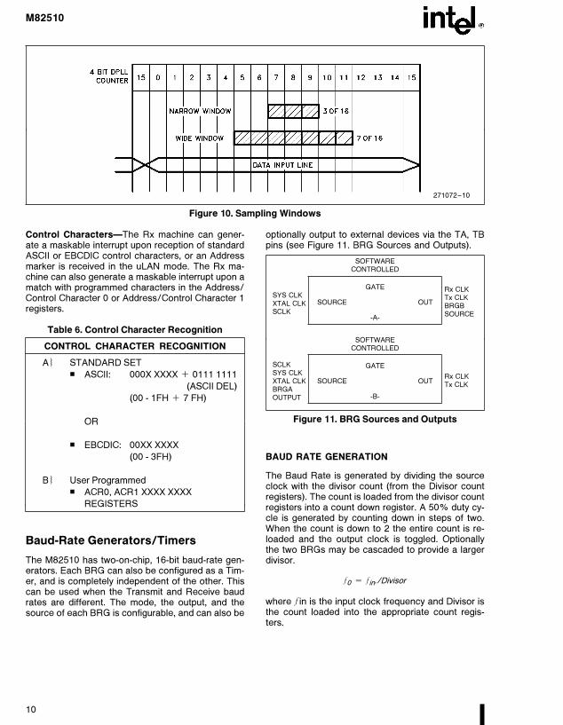
271072–10
Figure 10. Sampling Windows
Control CharactersÐThe Rx machine can gener-ate a maskable interrupt upon reception of standardASCII or EBCDIC control characters, or an Addressmarker is received in the uLAN mode. The Rx ma-chine can also generate a maskable interrupt upon amatch with programmed characters in the Address/Control Character 0 or Address/Control Character 1registers.
Table 6. Control Character Recognition
CONTROL CHARACTER RECOGNITION
AÓ STANDARD SETX ASCII: 000X XXXX a 0111 1111
(ASCII DEL)
(00 - 1FH a 7 FH)
OR
X EBCDIC: 00XX XXXX
(00 - 3FH)
BÓ User ProgrammedX ACR0, ACR1 XXXX XXXX
REGISTERS
Baud-Rate Generators/Timers
The M82510 has two-on-chip, 16-bit baud-rate gen-erators. Each BRG can also be configured as a Tim-er, and is completely independent of the other. Thiscan be used when the Transmit and Receive baudrates are different. The mode, the output, and thesource of each BRG is configurable, and can also be
optionally output to external devices via the TA, TBpins (see Figure 11. BRG Sources and Outputs).
SOFTWARECONTROLLED
GATE Rx CLKSYS CLK Tx CLK
SOURCE OUTXTAL CLK BRGBSCLK SOURCE
-A-
SOFTWARECONTROLLED
SCLK GATESYS CLK
Rx CLKXTAL CLK SOURCE OUT
Tx CLKBRGA
-B-OUTPUT
Figure 11. BRG Sources and Outputs
BAUD RATE GENERATION
The Baud Rate is generated by dividing the sourceclock with the divisor count (from the Divisor countregisters). The count is loaded from the divisor countregisters into a count down register. A 50% duty cy-cle is generated by counting down in steps of two.When the count is down to 2 the entire count is re-loaded and the output clock is toggled. Optionallythe two BRGs may be cascaded to provide a largerdivisor.
f0 e fin./Divisor
where f in is the input clock frequency and Divisor isthe count loaded into the appropriate count regis-ters.
10

M82510
Table 7. Standard Baud Rates
Bit Rate 16x Divisor%
Error
110 5236 (1474h) .007%
300 1,920 (780h) Ð
1200 480 (1E0h) Ð
2400 240 (F0h) Ð
9600 60 (3Ch) Ð
19,200 30 (1Eh) Ð
38,400 15 (0Fh) Ð
56,000 10 (0Ah) 2.8%
288,000 2 (02h) Ð
Source CLK e Internal Sys. Clke 18.432 MHz/2e 9.216 MHz
The BRG counts down in increments of two andthen is divided by two to generate a 50% duty cycle;however, for odd divisors it will count down the firsttime by one. All subsequent countdowns will thencontinue in steps of two. In those cases the dutycycle is no longer exactly 50%. The deviation is giv-en by the following equation:
deviation e 1/(2 X divisor)
The BRG can operate with any divisor between 1and 65,535; however, for divisors between 1 and 3the duty cycle is as follows:
Table 8. Duty Cycles
Divisor Duty Cycle
3 33%
2 50%
1 Same as Source
0 FORBIDDEN
Timer Mode
Each of the M82510 BRGs can be used as Timers.The Timer is used to generate time delays by count-ing the internal system clock. When enabled theTimer uses the count from the Divisor/Count regis-ters to count down to 1. Upon terminal count amaskable Timer Expired interrupt is generated. Thedelay between the trigger and the terminal count isgiven by the following equation:
Delay e Count X (System Clock Period)
To start counting, the Timer has to be triggered viathe Start Timer Command. To restart the Timer afterterminal count or while counting, the software has toissue the trigger command again. While counting theTimer can be enabled or disabled by using a soft-ware controlled Gate. It is also possible to output apulse generated upon terminal count through the TAor TB pins.
In 1X clock mode the only clock source available isthe SCLK pin. The serial machines (both Tx Machineand Rx Machine) can independently use one of twoclock modes, either 1X or 16X. Also no configurationchanges are allowed during operation as each writein the BRG configuration registers causes a resetsignal to be sent to the BRG logic. The mode orsource clocks may be changed only after a Hard-ware or Software reset. The Divisor (or count, de-pending upon the mode) may be updated during op-eration unless the particular BRG machine is beingused as a clock source for one of the serial ma-chines, and the particular serial machine is in opera-tion at the time. Loading the count registers with ‘‘0’’is forbidden in all cases, and loading it with a ‘‘1’’ isforbidden in the Timer Mode only.
SERIAL DIAGNOSTICS
The M82510 supports two modes of Loopback oper-ation, Local Loopback and Remote Loopback aswell as an Echo mode for diagnostics and improvedthroughput.
LOCAL LOOPBACK
271072–11
Figure 12. Local Loopback
The Tx Machine output and Rx Machine input areshorted internally, TXD pin output is held at Mark.This feature allows simulation of Transmission/Re-ception of characters and checks the Tx FIFO, TxMachine, Rx Machine, and Rx FIFO along with thesoftware without any external side effects. The mo-dem outputs OUT1, OUT2, DTR and RTS are inter-nally shorted to RI, DCD, DSR and CTS respectively.OUT0 is held at a mark state.
11

M82510
REMOTE LOOPBACK
271072–12
Figure 13. Remote Loopback
The TXD pin and RXD pin are shorted internally (thedata is not sent on to the RX Machine). This featureallows the user to check the communications chan-nel as well as the Tx and Rx pin circuits not checkedin the Local Loopback mode.
AUTO ECHO
271072–13
Figure 14. Auto Echo
In Echo Mode the received characters are automati-cally transmitted back. When the characters areread from the Rx FIFO they are automaticallypushed back onto the Tx FIFO (the flags are alsoincluded). The Rx Machine baud rate must be equalto, or less than, the Tx Machine baud rate or someof the characters may be lost. The user has an op-tion of preventing echo of special characters; Con-trol Characters and characters with Errors.
Power Down Mode
The M82510 has a ‘‘power down’’ mode to reducepower consumption when the device is not in use.
The M82510 powers down when the power downcommand is issued via the Internal Command Regis-ter (ICM). There are two modes of power down,Sleep and Idle.
In Sleep mode, even the system clock of theM82510 is shut down. The system clock source ofthe M82510 can either be the Crystal Oscillator oran external clock source. If the Crystal Oscillator isbeing used and the power down command is issued,then the M82510 will automatically enter the Sleepmode. If an external clock is being used, then theuser must disable the external clock in addition toissuing the Power Down command, to enter theSleep mode. The benefit of this mode is the in-creased savings in power consumption (typical pow-er consumption in the Sleep mode is in the ranges of100s of microAmps). However, upon wake up, theuser must reprogram the device. To exit this modethe user can either issue a Hardware reset, or readthe FIFO Level Register (FLR) and then issue a soft-ware reset. In either case the contents of theM82510 registers are not preserved and the devicemust be reprogrammed prior to operation. If theCrystal Oscillator is being used then the user mustallow enough time for the oscillator to wake up be-fore issuing the software reset.
The M82510 is in the idle mode when the PowerDown command is issued and the system clock isstill running (i. e. the system clock is generated ex-ternally and not disabled by the user). In this modethe contents of all registers and memory cells arepreserved, however, the power consumption in thismode is greater than in the Sleep mode. ReadingFLR will take the M82510 out of this mode.
NOTE:The data read from FLR when exiting Power Downis invalid and should be ignored.
12

M82510
DETAILED REGISTER DESCRIPTION
Table 9. Register Map
Bank AddressRead Write
Register Register
0 (NAS) 0 (DLAB e 0) RXD TXD
8250A/16450 1 (DLAB e 0) GER GER
0 (DLAB e 1) BAL BAL
1 (DLAB e 1) BAH BAH
2 GIR/BANK BANK
3 LCR LCR
4 MCR MCR
5 LSR LSR
6 MSR MSR
7 ACR0 ACR0
1 (WORK) 0 RXD TXD
1 RXF TXF
2 GIR/BANK BANK
3 TMST TMCR
4 FLR MCR
5 RST RCM
6 MSR TCM
7 GSR ICM
2 (GENERAL CONF) 0 Ð Ð
1 FMD FMD
2 GIR/BANK BANK
3 TMD TMD
4 IMD IMD
5 ACR1 ACR1
6 RIE RIE
7 RMD RMD
3 (MODEM CONF) 0 (DLAB e 0) CLCF CLCF
1 (DLAB e 0) BACF BACF
0 (DLAB e 1) BBL BBL
1 (DLAB e 1) BBH BBH
2 GIR/BANK BANK
3 BBCF BBCF
4 PMD PMD
5 MIE MIE
6 TMIE TMIE
7 Ð Ð
(1) ACRO is used in INS8250 as a Scratch-Pad Register
(2) DLAB e LCR Bit Ý7
The M82510 has thirty-five registers which are divided into four banks of register banks. Only one bank isaccessible at any one time. The bank is selected through the BANK1-0 bits in the GIR/BANK register. Theindividual registers within a bank are selected by the three address lines (A2–0). The M82510 registers can begrouped into the following categories.
13

M82510
BANK ZERO 8250A/16450ÐCOMPATIBLE BANK
Register 7 6 5 4 3 2 1 0 Address Default
TxD (33) Tx Data Tx Data Tx Data Tx Data Tx Data Tx Data Tx Data Tx Data 0 Ð
bit 7 bit 6 bit 5 bit 4 bit 3 bit 2 bit 1 bit 0
RxD (35) Rx Data Rx Data Rx Data Rx Data Rx Data Rx Data Rx Data Rx Data 0 Ð
bit 7 bit 6 bit 5 bit 4 bit 3 bit 2 bit 1 bit 0
BAL (11) BRGA LSB Divide Count (DLAB e 1) 0 02H
BAH (12) BRGA MSB Divide Count (DLAB e 1) 1 00H
GER (16) 0 0 Timer Tx Machine Modem Rx Machine Tx FIFO Rx FIFO 1 00H
Interrupt Interrupt Interrupt Interrupt Interrupt Interrupt
Enable Enable Enable Enable Enable Enable
GIR/BANK 0 BANK BANK 0 Active Active Active Interrupt 2 01H
(21) Pointer Pointer Block Int Block Int Block Int Pending
bit 1 bit 0 bit 2 bit 1 bit 0
LCR (2) DLAB Set Parity Parity Parity Stop bit Character Character 3 00H
Divisor Break Mode Mode Mode Length Length Length
Latch bit 2 bit 1 bit 0 bit 0 bit 1 bit 0
Access bit
MCR (32) 0 0 OUT 0 Loopback OUT 2 OUT 1 RTS DTR 4 00H
Complement Control bit Complement Complement Complement Complement
LSR (22) 0 TxM Tx FIFO Break Framing Parity Overrun Rx FIFO 5 60H
Idle Interrupt Detected Error Error Error Int Req
MSR (27) DCD Input RI Input DSR Input CTS Input State State (HxL) State State 6 00H
Inverted Inverted Inverted Inverted Change Change Change Change
in DCD in RI in DSR in CTS
ACR0 (5) Address or Control Character Zero 7 00H
BANK ONEÐGENERAL WORK BANK
Register 7 6 5 4 3 2 1 0 Address Default
TxD (33) Tx Data Tx Data Tx Data Tx Data Tx Data Tx Data Tx Data Tx Data 0 Ð
bit 7 bit 6 bit 5 bit 4 bit 3 bit 2 bit 1 bit 0
RxD (35) Rx Data Rx Data Rx Data Rx Data Rx Data Rx Data Rx Data Rx Data 0 Ð
bit 7 bit 6 bit 5 bit 4 bit 3 bit 2 bit 1 bit 0
RxF (24) Ð Rx Char Rx Char Rx Char Address or Break Rx Char Ninth 1 Ð
OK Noisy Parity Control Flag Framing Data bit
Error Character Error of Rx Char
TxF (34) Address Software Ninth bit 0 0 0 0 0 1 Ð
Marker bit Parity bit of Data Char
GIR/BANK 0 BANK BANK 0 Active Active Active Interrupt 2 01H
(21) Pointer Pointer Block Int Block Int Block Int Pending
bit 1 bit 0 bit 2 bit 1 bit 0
TMST (26) Ð Ð Gate B Gate A Ð Ð Timer B Timer A 3 30H
State State Expired Expired
TMCR (31) 0 0 Trigger Trigger 0 0 Start Start 3 Ð
Gate B Gate A Timer B Timer A
MCR (32) 0 0 OUT 0 Loopback OUT 2 OUT 1 RTS DTR 4 00H
Complement Control bit Complement Complement Complement Complement
NOTE:The register number is provided as a reference number for the register description.
14

M82510
BANK ONEÐGENERAL WORK BANK (Continued)
Register 7 6 5 4 3 2 1 0 Address Default
FLR (25) Ð Rx FIFO Level Ð Tx FIFO Level 4 00H
RST (23) Address/ Address/ Break Break Framing Parity Overrun Rx FIFO 5 00H
Control Control Terminated Detected Error Error Error Interrupt
Character Character Requested
Received Match
RCM (30) Rx Rx Flush Flush Lock Rx Open Rx 0 0 5 Ð
Enable Disable RxM Rx FIFO FIFO FIFO
MSR (27) DCD RI Input DSR Input CTS Input State State State State 6 00H
Complement Inverted Inverted Inverted Change Change Change Change
in DCD in RI in DSR in CTS
TCM (29) 0 0 0 0 Flush Tx Flush Tx Tx Tx 6 Ð
Machine FIFO Enable Disable
GSR (20) Ð Ð Timer TxM Modem RxM Tx FIFO Rx FIFO 7 12H
Interrupt Interrupt Interrupt Interrupt Interrupt Interrupt
ICM (28) 0 0 0 Software Manual Int Status Power 0 7 Ð
Reset Acknowledge Clear Down
Command Mode
BANK TWOÐGENERAL CONFIGURATION
Register 7 6 5 4 3 2 1 0 Address Default
FMD (4) 0 0 Rx FIFO Threshold 0 0 Tx FIFO Threshold 1 00H
GIR/BANK 0 BANK BANK 0 Active Active Active Interrupt 2 01H
(21) Pointer Pointer Block Int Block Int Block Int Pending
bit 1 bit 0 bit 2 bit 1 bit 0
TMD (3) Error Control 9-bit Transmit Mode Software Stop Bit Length 3 00H
Echo Character Character Parity
Disable Echo Disable Length Mode
IMD (1) 0 0 0 0 Interrupt Rx FIFO ulan Loopback or 4 0CH
Acknowledge Depth Mode Echo Mode
Mode Select of Operation
ACR1 (6) Address or Control Character 1 5 00H
RIE (17) Address/ Address/ Break Break Framing Parity Overrun 0 6 1EH
Control Control Terminate Detect Error Error Error
Character Character Interrupt Interrupt Interrupt Interrupt Interrupt
Recognition Match Enable Enable Enable Enable Enable
Interrupt Interrupt
Enable Enable
RMD (7) Address/Control Disable Sampling Start bit 0 0 0 7 00H
Character Mode DPLL Window Sampling
Mode Mode
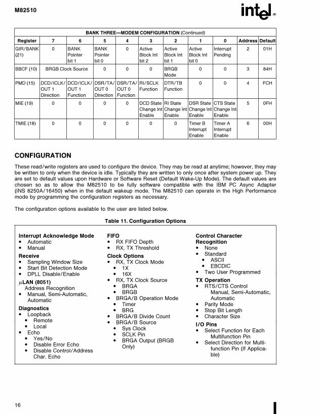
BANK THREEÐMODEM CONFIGURATION
Register 7 6 5 4 3 2 1 0 Address Default
CLCF (8) Rx Clock Rx Clock Tx Clock Tx Clock 0 0 0 0 0 00H
Mode Source Mode Source
BACF (9) 0 BRGA 0 0 0 BRGA 0 0 1 04H
Clock Mode
Source
BBL (13) BRGB LSB Divide Count (DLAB e 1) 0 05H
BBH (14) BRGB MSB Divide Count (DLAB e 1) 1 00H
15
M82510
BANK THREEÐMODEM CONFIGURATION (Continued)
Register 7 6 5 4 3 2 1 0 Address Default
GIR/BANK 0 BANK BANK 0 Active Active Active Interrupt 2 01H
(21) Pointer Pointer Block Int Block Int Block Int Pending
bit 1 bit 0 bit 2 bit 1 bit 0
BBCF (10) BRGB Clock Source 0 0 0 BRGB 0 0 3 84H
Mode
PMD (15) DCD/ICLK/ DCD/ICLK/ DSR/TA/ DSR/TA/ RI/SCLK DTR/TB 0 0 4 FCH
OUT 1 OUT 1 OUT 0 OUT 0 Function Function
Direction Function Direction Function
MIE (19) 0 0 0 0 DCD State RI State DSR State CTS State 5 0FH
Change Int Change Int Change Int Change Int
Enable Enable Enable Enable
TMIE (18) 0 0 0 0 0 0 Timer B Timer A 6 00H
Interrupt Interrupt
Enable Enable
CONFIGURATION
These read/write registers are used to configure the device. They may be read at anytime; however, they maybe written to only when the device is idle. Typically they are written to only once after system power up. Theyare set to default values upon Hardware or Software Reset (Default Wake-Up Mode). The default values arechosen so as to allow the M82510 to be fully software compatible with the IBM PC Async Adapter(INS 8250A/16450) when in the default wakeup mode. The M82510 can operate in the High Performancemode by programming the configuration registers as necessary.
The configuration options available to the user are listed below.
Table 11. Configuration Options
Interrupt Acknowledge Mode# Automatic# Manual
Receive# Sampling Window Size# Start Bit Detection Mode# DPLL Disable/Enable
mLAN (8051)Address Recognition
# Manual, Semi-Automatic,Automatic
Diagnostics# Loopback
# Remote# Local
# Echo# Yes/No# Disable Error Echo# Disable Control/Address
Char. Echo
FIFO# RX FIFO Depth# RX, TX Threshold
Clock Options# RX, TX Clock Mode
# 1X# 16X
# RX, TX Clock Source# BRGA# BRGB
# BRGA/B Operation Mode# Timer# BRG
# BRGA/B Divide Count# BRGA/B Source
# Sys Clock# SCLK Pin# BRGA Output (BRGB
Only)
Control CharacterRecognition# None# Standard
# ASCII# EBCDIC
# Two User Programmed
TX Operation# RTS/CTS Control
Manual, Semi-Automatic,Automatic
# Parity Mode# Stop Bit Length# Character Size
I/O Pins# Select Function for Each
Multifunction Pin# Select Direction for Multi-
function Pin (If Applica-ble)
16

M82510
1. IMDÐINTERNAL MODE REGISTER
IMDÐInternal Mode Register
271072–14
This register defines the general device mode of op-eration. The bit functions are as follows:
7–4: Reserved
IAM: Interrupt Acknowledge Mode Bit
0 Ð Manual acknowledgement of pend-ing interrupts
1 Ð Automatic acknowledgement ofpending interrupts (upon CPU serv-ice)
This bit, when set, configures the M82510 for theautomatic acknowledge mode. This causes theM82510 INT line to go low for two clock cycles uponservice of the interrupt. After two clock cycles it isthen updated. It is useful in the edge triggered mode.In manual acknowledgement mode the CPU mustexplicitly issue a command to clear the INT pin. (TheINT pin then goes low for a minimum of two clockcycles until another enabled status register bit isset.)
RFD: Receive FIFO Depth
0 Ð Four Bytes1 Ð One Byte
This bit configures the depth of the Rx FIFO. With aFIFO depth of one, the FIFO will act as a 1-bytebuffer to emulate the 8250A.
ULM: uLAN Mode
0 Ð Normal Mode1 Ð uLAN Mode
This bit, enables the M82510 to recognize and/ormatch address using the 9-bit MCS-51 asynchro-nous protocol.
LEM: Loopback/Echo Mode Select
This bit selects the mode of loopback operation, orthe mode of echo operation; depending upon whichoperation mode is selected by the Modem Controlregister bit LC.
In loopback mode (Modem Control register bitLC e 1) it selects between local and remote loop-back.
0 Ð Local Loopback1 Ð Remote Loopback
Inecho mode (Modem Control register bit LC e 0) itselects between echo or non-echo operation.
0 Ð No Echo1 Ð Echo Operation
17

M82510
2. LCRÐLINE CONFIGURE REGISTER
LCRÐLine Configure Register
271072–15
This register defines the basic configuration of theserial link.
DLABÐDivisor Latch Access BitÐThis bit, whenset, allows access to the Divisor Count registersBAL,BAH;BBL,BBH registers.
SBKÐSet Break BitÐThis bit will force the TxD pinlow. The TxD pin will remain low (regardless of allactivities) until this bit is reset.
PM2ÐPM0ÐParity Mode BitsÐThese three bitscombine with the SPF bit of the Transmit Mode reg-ister to define the various parity modes. See Table12.
Table 12. Parity Modes
PM0 SPF PM2 PM1 Function
0 X X X No Parity
1 0 0 0 Odd Parity
1 0 0 1 Even Parity
1 0 1 0 High Parity
1 0 1 1 Low Parity
1 1 0 0 Software Parity
SBLOÐStop Bit LengthÐThis bit, together withSBL1 and SBL2 bits of the Transmit Mode register,defines the Stop-bit lengths for transmission. The Rxmachine can identify 3/4 stop bit or more. See Table13.
Table 13. Stop Bit Length
SBL2 SBL1 SBL0Stop Bit Length
16X 1X
0 0 0 4/4 Ð
0 0 1 6/4 or 8/4* Ð
0 1 0 3/4 1
0 1 1 4/4 1
1 0 0 5/4 1
1 0 1 6/4 1
1 1 0 7/4 1
1 1 1 8/4 2
*6/4 if character length is 5 bits; else 8/4
CL0ÐCL1ÐCharacter Length BitsÐThese bits,together with the Transmit Mode register bit NBCL,define the character length. See Table 14.
Table 14. Character Length
NBCL CL1 CL0 Character Length
0 0 0 5 BITS
0 0 1 6 BITS
0 1 0 7 BITS
0 1 1 8 BITS
1 0 0 9 BITS
18

M82510
3. TMDÐTransmit Machine Mode Register
TMDÐTransmit Machine Mode Register
271072–16
This register together with the Line Configure Regis-ter defines the Tx machine mode of operation.
EEDÐError Echo DisableÐDisables Echo of char-acters received with errors (valid in echo modeonly).
CEDÐControl Character Echo DisableÐDisablesEcho of characters recognized as control characters(or address characters in uLAN mode). Valid in echomode only.
NBCLÐNine-Bit LengthÐThis bit, coupled withLCR (CL0, CL1), selects Transmit/Receive charac-ter length of nine bits. See Table 14.
TM1ÐTM0ÐTransmit ModeÐThese bits selectone of three modes of control over the CTS andRTS lines.
00ÐManual ModeÐIn this mode the CPU has fullcontrol of the Transmit operation. The CPU has toexplicitly enable/disable transmission, and activate/check the RTS/CTS pins.
01ÐReserved
10ÐSemi-Automatic ModeÐIn this mode theM82510 transmits only when CTS input is active.The M82510 activates the RTS output as long astransmission is enabled.
11ÐAutomatic ModeÐIn this mode the M82510transmits only when CTS input is active. The RTSoutput is activated only when transmission is en-abled and there is more data to transmit.
SPFÐSoftware Parity ForceÐThis bit defines theparity modes along with the PM0, PM1, and PM2 bitsof the LCR register. When software parity is enabledthe software must determine the parity bit throughthe TxF register on transmission, or check the paritybit in RxF upon reception. See Table 12.
SBL2ÐSBL1ÐStop Bit LengthÐThese bits, to-gether with the SBL0 bit of the LCR register definethe stop bit length. See Table 13.
19
M82510
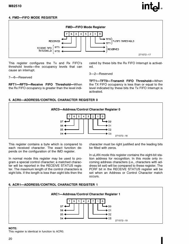
4. FMDÐFIFO MODE REGISTER
FMDÐFIFO Mode Register
271072–17
This register configures the Tx and Rx FIFO’sthreshold levelsÐthe occupancy levels that cancause an interrupt.
7Ð6ÐReserved
RFT1ÐRFT0ÐReceive FIFO ThresholdÐWhenthe Rx FIFO occupancy is greater than the level indi-
cated by these bits the Rx FIFO Interrupt is activat-ed.
3Ð2ÐReserved
TFT1ÐTFT0ÐTransmit FIFO ThresholdÐWhenthe TX FIFO occupancy is less than or equal to thelevel indicated by these bits the Tx FIFO Interrupt isactivated.
5. ACR0ÐADDRESS/CONTROL CHARACTER REGISTER 0
ARC0ÐAddress/Control Character Register 0
271072–18
This register contains a byte which is compared toeach received character. The exact function de-pends on the configuration of the IMD register.
In normal mode this register may be used to pro-gram a special control character; a matched charac-ter will be reported in the RECEIVE STATUS regis-ter. The maximum length of the control characters iseight bits. If the length is less than eight bits then the
character must be right justified and the leading bitsbe filled with zeros.
In uLAN mode this register contains the eight-bit sta-tion address for recognition. In this mode only in-coming address characters (i.e., characters with ad-dress bit set) will be compared to these register. ThePCRF bit in the RECEIVE STATUS register will beset when an Address or Control Character matchoccurs.
6. ACR1ÐADDRESS/CONTROL CHARACTER REGISTER 1
ARC1ÐAddress/Control Character Register 1
271072–19
NOTE:This register is identical in function to ACR0.
20

M82510
7. RMDÐRECEIVE MACHINE MODE REGISTER
RMDÐReceive Machine Mode Register
271072–20
This register defines the Rx Machine mode of opera-tion.
uCM0, uCM1ÐuLAN/Control Character Recogni-tion ModeÐIn normal mode it defines the ControlCharacter recognition mode. In ulan mode they de-fine modes of address recognition.
In uLAN mode: selects the mode of address recog-nition.
00ÐManual ModeÐRx Machine reports receptionof any address character, via CRF bit of RECEIVESTATUS register, and writes it to the Rx FIFO.
01ÐSemi-Automatic ModeÐOperates the sameas Manual Mode but, in addition, the Rx MachineOPENS (unlocks) the Rx FIFO upon reception of anyaddress characters. Subsequent received charac-ters will be written into the FIFO. (Note: it is the us-er’s responsibility to LOCK the FIFO if the addresscharacter does not match the station’s address.)
10ÐAutomatic ModeÐThe Rx Machine will OPEN(unlock) the Rx FIFO upon Address Match. In addi-tion the Rx Machine LOCKs the Rx FIFO upon rec-ognition of address mismatch; i.e., it controls theflow of characters into the Rx FIFO depending uponthe results of the address comparison. If a matchoccurs it will allow characters to be sent to the FIFO;if a mismatch occurs it will keep the characters outof the FIFO by LOCKING it.
11ÐReserved
In normal Mode: selects the mode of Standard SetControl Character Recognition (programmed controlcharacters are always recognized).
00Ð No Standard Set Control Characters Recog-nized.
01Ð ASCII Control Characters(00HÐ1 FH a 7FH).
10Ð Reserved.
11Ð EBCDIC Control Character Recognized(00H b 3FH).
DPDÐDisable Digital Phase Locked LoopÐWhenset, disables the DPLL machine. (Note: using theDPLL in a very noisy media, may increase the errorrate.)
SWMÐSampling Window ModeÐThis bit controlsthe mode of data sampling:
0ÐSmall Window, 3/16 sampling.1ÐLarge Window, 7/16 sampling.
SSMÐStart Bit Sampling ModeÐThis bit controlsthe mode of Start Bit sampling.
0Ð Majority Voting for start bit. In this mode a ma-jority of the samples determines the bit.
1Ð In this mode if one of the bit samples is not‘0’, the start bit will not be detected.
21

M82510
8. CLCFÐCLOCKS CONFIGURE REGISTER
CLCFÐClocks Configure Register
271072–21
This register defines the Transmit and Receive Codemodes and sources.
RxCMÐRx Clock ModeÐThis bit selects the modeof the receive clock which is used to sample thereceived data.
0Ð 16X Mode.1Ð 1X Mode. In this mode the receive data must be
synchronous to the Rx Clock; supplied via theSCLK pin.
RxCSÐRx Clock SourceÐThis bit selects thesource of the internal receive clock in the case of16X mode (as programmed by the RxCM bit above).
0ÐBRGB Output1ÐBRGA Output
TxCMÐTransmit Clock ModeÐThis bit selects themode of the Transmit Data Clock, which is used toclock out the Transmit Data.
0Ð 16X Mode
1Ð 1X Mode. In this mode the Transmit data issynchronous to the Serial Clock; supplied viathe SCLK pin.
TxCSÐTransmit Clock SourceÐSelects thesource of internal Transmit Clock in case of 16Xmode.
0ÐBRGB Output.1ÐBRGA Output.
9. BACFÐBRGA CONFIGURATION REGISTER
BACFÐBRGA Configuration Register
271072–22
This register defines the BRGA clock sources andthe mode of operation.
BACSÐBRGA Clock SourceÐSelects the inputclock source for Baud Rate Generator A.
0ÐSystem Clock1ÐSCLK Pin
This bit has no effect if BRGA is configured as atimer.
BAMÐBRGA Mode of OperationÐSelects be-tween the Timer mode or the Baud Rate GeneratorMode.
0Ð Timer Mode (in this mode the input clocksource is always the system clock).
1Ð Baud Rate Generator Mode
22

M82510
10. BBCFÐBRGB CONFIGURATION REGISTER
BBCFÐBRGB Configuration Register
271072–23
This register defines the BRGB clock sources andmode of operation. (Note: BRGB can also take itsInput Clock from the output of BRGA.)
BBCS1, BBCS0ÐThese two bits together define theinput Clock Sources for BRGB. These bits have noeffect when in the timer mode.
00Ð System Clock01Ð SCLK Pin
10Ð BRGA Output11Ð Reserved
BBMÐBRGB Mode of Operation.
0Ð Timer Mode (In this mode the input clocksource is always the system clock.)
1Ð BRG Mode
11. BALÐBRGA DIVIDE COUNT LEAST SIGNIFICANT BYTE
BALÐBRGA Divide Count Low Byte
271072–24
This register contains the least significant byte of the BRGA divisor/count.
12. BAHÐBRGA DIVIDE COUNT MOST SIGNIFICANT BYTE
BAHÐBRGA Divide Count High Byte
271072–25
This register contains the most significant byte of the BRGA divisor/count.
13. BBLÐBRGB DIVIDE COUNT LEAST SIGNIFICANT BYTE
BBLÐBRGB Divide Count Low Byte
271072–26
This register contains the least significant byte of the BRGB divisor/count.
23

M82510
14. BBHÐBRGB DIVIDE COUNT MOST SIGNIFICANT BYTE
BBHÐBRGB Divide Count High Byte
271072–27
This register contains the most significant byte of the BRGB divisor/count.
15. PMDÐI/O PIN MODE REGISTER
PMDÐI/O Pin Mode Register
271072–28
This register is used to configure the direction andfunction of the multifunction pins. The following op-tions are available on each pin.
1. Direction: Input or Output Pin.0Ð Defines the Pin as an output pin (general pur-
pose or special function).1Ð Defines the pin as an input pin.
2. Function: General purpose or special purpose pin(no effect if the pin is programmed as an Input).
0Ð special function output pin.1Ð general purpose output pin.
DIODÐDCD/ICLK/OUT1 Direction.
0Ð Output: ICLK or OUT1 (depending on bitDIOF)
1Ð Input: DCD.DIOFÐDCD/ICLK/OUT1 Function (outputmode only).
0Ð ICLK (Output of the Internal System Clock).1Ð OUT1 general purpose output, Controlled by
MODEM CONTROL RegisterDTADÐDSR/TA/OUT0 Direction.
0Ð Output: TA or OUT0 (Dependent uponDTAF).
1Ð Input: DSR.DTAFÐDSR/TA/OUT0 Direction (outputmode only).
0Ð TA (BRGA Output or Timer A TerminationPulse).
1Ð OUT0 (general purpose output, controlled byMODEM CONTROL).RRFÐRI/SCLK Function
0Ð SCLK (Receive and/or Transmit Clock)1Ð RI
DTFÐDTR/TB Function
0Ð TB (BRGB Output Clock on Timer B termina-tion pulse depending upon the mode ofBRGB).
1Ð DTR
24

M82510
INTERRUPT/STATUS REGISTERS
The M82510 uses a two layer approach to handleinterrupt and status generation. Device level regis-ters show the status of the major M82510 functionalblock (MODEM, FIFO, Tx MACHINE, Rx MACHINE,TIMERS, etc.). Each block may be examined byreading its individual block level registers. Also eachblock has interrupt enable/generation logic whichmay generate a request to the built-in interrupt con-troller, the interrupt requests are then resolved on apriority basis.
Interrupt Masking
The M82510 has a device enable register, GER,which can be used to enable or mask-out any blockinterrupt request. Some of the blocks (Rx Machine,Modem, Timer) have an enable register associatedwith their status register which can be used to maskout the individual sources within the block. Interruptsare enabled when programmed high.
16. GERÐGENERAL ENABLE REGISTER
GERÐGeneral Enable Register
271072–29
This register enables or disables the bits of the GSRregister from being reflected in the GIR register. Itserves as the device enable register and is used tomask the interrupt requests from any of the M82510block (See Figure 1).
TIEÐTimers Interrupt Enable
TxIEÐTransmit Machine Interrupt Enable.
MIEÐModem Interrupt Enable.
RxIEÐRx Machine Interrupt Enable.
TFIEÐTransmit FIFO Interrupt Enable.
RFIEÐReceive FIFO Interrupt Enable.
17. RIEÐRECEIVE INTERRUPT ENABLE REGISTER
RIEÐReceive Interrupt Enable Register
271072–30
This register enables interrupts from the Rx Ma-chine. It is used to mask out interrupt requests gen-erated by the status bits of the RST register.
CREÐControl/uLAN Address Character Recog-nition Interrupt Enable.ÐEnables Interrupt whenCRF bit of RST register is set.
PCREÐProgrammable Control/Address Charac-ter Match Interrupt Enable.ÐEnables Interrupt onPCRF bit of RST.
BkTeÐBreak Termination Interrupt Enable.
BkDEÐBreak Detection Interrupt EnableÐEn-able Interrupt on BkD bit of RST.
FEEÐFraming Error EnableÐEnable Interrupt onFE bit of RST.
PEEÐParity Error EnableÐEnable Interrupt on PEbit of RST.
OEEÐOverrun Error EnableÐEnable Interrupt onOE bit of RST.
25

M82510
18. TMIEÐTIMER INTERRUPT ENABLE REGISTER
TMIEÐTimers/Interrupt Enable Register
271072–31
This is the enable register for the Timer Block. It isused to mask out interrupt requests generated bythe status bits of the TMST register.
TBIEÐTimer B Expired Interrupt EnableÐEn-ables Interrupt on TBEx bit of TMST.
TAIEÐTimer A Expired Interrupt EnableÐEn-ables Interrupt on TAEx bit of TMST.
19. MIEÐMODEM INTERRUPT ENABLE REGISTER
MIEÐModem Interrupt Enable Register
271072–32
This register enables interrupts from the ModemBlock. It is used to mask out interrupt requests gen-erated by the status bits of the MODEM STATUSregister.
DCDEÐDelta DCD Interrupt EnableÐEnables In-terrupt on DDCD bit of MODEM STATUS.
RIEÐDelta RI Interrupt EnableÐEnables Interrupton DRI bit of MODEM STATUS.
DSREÐDelta DSR Interrupt EnableÐEnables In-terrupt on DSR bit of MODEM STATUS.
CTSEÐDelta CTS Interrupt EnableÐEnables In-terrupt on DCTS bits of MODEM STATUS.
STATUS/INTERRUPT
The M82510 has two device status registers, whichreflect the overall status of the device, and five blockstatus registers. The two device status registers,GSR and GIR, and supplementary in function. GSRreflects the interrupt status of all blocks, whereasGIR depicts the highest priority interrupt only. GIR isupdated after the GSR register; the delay is of ap-proximately two clock cycles.
26

M82510
20. GSRÐGENERAL STATUS REGISTER
GSRÐGeneral Status Register
271072–33
This register reflects all the pending block-level In-terrupt requests. Each bit in GSR reflects the statusof a block and may be individually enabled by GER.GER masks-out interrupts from GIR; it does nothave any effect on the bits in GSR. The only waythat the bits can be masked out in GSR (i.e., notappear in GSR) is if they are masked out at the lowerlevel.
TIRÐTimers Interrupt RequestÐThis bit indicatesthat one of the timers has expired. (See TMST)
TxIRÐTransmit Machine Interrupt RequestÐIn-dicates that the Transmit Machine is either empty ordisabled (Idle).
MIRÐModem Interrupt RequestÐThis bit, if set,indicates an interrupt from the Modem Module. (Asreflected in MODEM STATUS.)
RxIRÐReceive Machine Interrupt RequestÐ(Asreflected in RST.)
TFIRÐTransmit FIFO Interrupt RequestÐTxFIFO occupancy is below or equal to threshold.
RFIRÐReceive FIFO Interrupt RequestÐRx FIFOOccupancy is above threshold.
21. GIR/BANKÐGENERAL INTERRUPT REGISTER/BANK REGISTER
General Interrupt Register/Bank Register
271072–34
This register holds the highest priority enabled pend-ing interrupt from GSR. In addition it holds a pointerto the current register segment. Writing into this reg-ister will update only the BANK bits.
BANK1, BANK0ÐBank Pointer BitsÐThese twobits point to the currently accessible register bank.The user can read and write to these bits. The ad-dress of this register is always two within all fourregister banks.
BI2, BI1, BI0,ÐInterrupt Bits 0–2ÐThese threebits reflect the highest priority enabled pending inter-rupt from GSR.
101: Timer Interrupt (highest priority)100: Tx Machine Interrupt011: Rx Machine Interrupt010: Rx FIFO Interrupt001: Tx FIFO Interrupt000: Modem Interrupt (lowest priority)
IPNÐInterrupt PendingÐThis bit is active low. Itindicates that there is an interrupt pending. The in-terrupt logic asserts the INT pin as soon as this bitgoes active. (Note: the GIR register is continuouslyupdated; so that, while the user is serving one inter-rupt source, a new interrupt with higher priority mayenter GIR and replace the older interrupt.)
27

M82510
22. LSRÐLINE STATUS REGISTER
LSRÐLine Status Register
271072–35
This register holds the status of the serial link. Itshares five of its bits with the RST register (BkD, FE,PE, OE, and RFIR). When this register is read, theRST register (BITS 1–7) and LSR register (BITS 1–4) are cleared. This register is provided for compati-bility with the INS8250A.
TxStÐTransmit Machine Status BitÐSame asTxIR bit of GSR register. If high it indicates that theTransmit Machine is in Idle State. (Note: Idle mayindicate that the TxM is either empty or disabled.
TFStÐTransmit FIFO StatusÐSame as TFIR bit ofGSR. It indicates that the Transmit FIFO level isequal to or below the Transmit FIFO Threshold.There are two ways to disable the transmit FIFOstatus from being reflected in GIR:
1. Writing a ‘‘0’’ to the TFIE bit of the GER register
2. Dynamically by using the Tx FIFO HOLD IN-TERRUPT logic. When the Tx FIFO is in theHold State, no interrupts are generated regard-less of the TFIR and TFIE bits.
The Transmit FIFO enters the Hold State when theCPU reads the GIR register and the source of theinterrupt is Tx FIFO. To Exit, the CPU must drop the
TFIR bit of GSR by writing a character to Tx FIFO, ordrop TFIE bit of GER (Disable Tx FIFO).
BkdÐBreak DetectedÐSee Bkd bit in RST registerfor full explanation. The BkD bit in RST register isthe same as this bit.
FEÐFraming Error DetectedÐSee FE bit in RSTregister for a full explanation. The FE bit in RST reg-ister is the same as this bit.
PEÐParity Error DetectedÐSee PE bit in RSTregister for full explanation. The PE bit in RST regis-ter is the same as this bit.
OEÐOverrun ErrorÐSee OE bit in RST register forfull explanation. The OE bit in RST register is thesame as this bit.
RFIRÐReceive FIFO Interrupt RequestÐThis bitis identical to RFIR bit of GSR. It indicates that theRX FIFO level is above the Rx FIFO Threshold. Thisbit is forced LOW during any READ from the RxFIFO. A zero written to this bit will acknowledge anRx FIFO interrupt.
28

M82510
23. RSTÐRECEIVE MACHINE STATUS REGISTER
RSTÐReceive Machine Status Register
271072–36
This register displays the status of the Receive Ma-chine. It reports events that have occurred since theRST was cleared. This register is cleared when it isread except for BIT0, Rx FIFO interrupt. Each bit inthis register, when set, can cause an interrupt. Fivebits of this register are shared with the LSR register.
CRFÐControl/Address Character ReceivedÐWhen enabled, this bit can cause an interrupt if acontrol character or address character is received.
In uLAN Mode: indicates that an address charac-ter has been received.In normal Mode: indicates that a standard controlcharacter (either ASCII or EBCDIC) has been re-ceived.
PCRFÐProgrammed Control/Address CharacterReceivedÐThis bit, when enabled, will cause an in-terrupt when an address or control character matchoccurs.
In uLAN Mode: indicates that an address charac-ter equal to one of the registers ACR0 or ACR1has been received.
In normal Mode: indicates that a character whichmatches the registers ACR0 or ACR1 has beenreceived.
BkTÐBreak TerminatedÐThis bit indicates that abreak condition has been terminated.
BkDÐBreak DetectedÐThis bit indicates that aBreak Condition has been detected, i.e., RxD inputwas held low for one character frame plus a stopBIT.
FEÐFraming ErrorÐThis bit indicates that a re-ceived character did not have a valid stop bit.
PEÐParity ErrorÐIndicates that a received charac-ter had a parity error.
OEÐOverrun ErrorÐIndicates that a receivedcharacter was lost because the Rx FIFO was full.
RFIRÐReceive FIFO Interrupt RequestÐSameas the RFIR bit of LSR register.
29

M82510
24. RXFÐRECEIVED CHARACTER FLAGS
RxFÐReceive Flags Register
271072–37
This register contains additional information aboutthe character in the RXD register. It is loaded by theRx Machine simultaneously with the RXD register.
ROKÐReceived Character OKÐThis bit indicatesthat the character in RXD no parity or framing error.The parity error is not included in the s/w paritymode.
RxNÐReceived Character NoisyÐThe characterin RXD was noisy. This bit, valid only in 16X sam-pling mode, indicates that the received characterhad non-identical samples for at least one of its bits.
RPEÐReceive Character Parity ErrorÐThis bit in-dicates that the RxD character had a Parity Error.However, in S/W Parity mode it holds the receivedparity bit as is.
ACRÐAddress/Control Character MarkerÐThisbit indicates that the character in RXD is either:
A control CharacterÐin normal Mode.An Address Character in uLAN Mode.
RFEÐReceive Character Framing ErrorÐIndi-cates that no Stop bit was found for the character inRXD.
NOTE:A Framing Error will be generated for the first char-acter of the Break sequence.
RNDÐNinth Bit of Received CharacterÐThemost significant bit of the character in RXD is writteninto this bit. This bit is zero for characters with lessthan nine bits.
BKFÐBreak FlagÐIndicates that the character ispart of a ‘‘break’’ sequence.
25. FLRÐFIFO LEVEL REGISTER
FLRÐFIFO Level Register
271072–38
This register holds the current Receive and TransmitFIFO occupancy levels.
RFL2, RFL1, RFL0ÐReceive FIFO Level of Occu-pancyÐThese three bits indicate the level of Occu-
pancy of the Rx FIFO. The valid range is zero (000)to four (100).
TFL2, TFL1, TFL0ÐTransmit FIFO Level of Occu-pancyÐThese three bits indicate the level of occu-pancy in the transmit FIFO. The valid range is zero(000) to four (100).
30

M82510
26. TMSTÐTIMER STATUS REGISTER
TMSTÐTimer Status Register
271072–39
This register holds the status of the timers. BitsTBEx and TAEx generate interrupts which are re-flected in bit TIR of GSR. Bits GBS and GAS justdisplay the counting status, they do not generate in-terrupts.
GBSÐGate B StateÐThis bit does not generate aninterrupt. It indicates the counting state of the soft-ware gate of Timer B, as written through the TMCRregister.
0Ðcounting disabled1Ðcounting enabled
GASÐGateÐA StateÐThis bit does not generatean interrupt. It reflects the state of the software gateof Timer A, as written through the TMCR register.
0Ðcounting disabled1Ðcounting enabled
TBExÐTimer B ExpiredÐWhen Set generates aninterrupt through TIR bit of GSR. Indicates that Tim-er B count has expired. This bit is set via the terminalcount pulse generated by the timer when it termi-nates counting.
TAExÐTimer A ExpiredÐSame as TBEx except itrefers to Timer A.
27. MSRÐMODEM/I/O PINS REGISTER
MSRÐModem/I/O Pins Status Register
271072–40
This register holds the status of the Modem inputpins (CTS, DCD, DSR, RI). It is the source of inter-rupts (MSR 0–3) for the MIR bit of GSR. If any of theabove inputs change levels the appropriate bit inMODEM STATUS is set. Reading MODEM STATUSwill clear the status bits.
DCDCÐDCD ComplementÐHolds the comple-ment of the DCD input pin if programmed as an inputin PMD.
DRICÐHolds the complement of the RI input pin ifprogrammed as an input in PMD.
DSRCÐDSR ComplementÐHolds the complementof the DSR input pin if configured as an input inPMD.
CTSCÐCTS ComplementÐHolds the complementof the CTS pin.
DDCDÐDelta DCDÐIndicates that the DCD inputpin has changed state since this register was lastread.
DRIÐDelta RIÐIndicates that there was a high-to-low transition on the RI input pin since the registerwas last read.
DDSRÐDelta DSRÐIndicates that the DSR inputpin has changed state since this register was lastread.
DCTSÐDelta CTSÐIndicates that the CTS inputpin has changed state since this register was lastread.
COMMAND REGISTERS
The command registers are write only; they are usedto trigger an operation by the device. Once the oper-ation is started the register is automatically reset.There is a device level register as well as four blockcommand registers. It is recommended that only onecommand be issued during a write cycle.
31

M82510
28. ICMÐINTERNAL COMMAND REGISTER
ICMÐInternal Command Register
271072–41
This register activates the device’s general func-tions.
SRSTÐDevice Software RESETÐCauses a totaldevice reset; the effect is identical to the hardwarereset (except for strapping options). The reset lastsfour clocks and puts the device into the DefaultWake-up Mode.
INTAÐInterrupt AcknowledgeÐThis command isan explicit acknowledgement of the M82510’s inter-rupt request. It forces the INT pin inactive for two
clocks; afterwards, the INT pin may again go active ifother enabled interrupts are pending. This commandis provided for the Manual Acknowledge mode ofthe M82510.
StCÐStatus ClearÐClears the following status reg-isters: RST, MSR, and TMST.
PDMÐPower DownÐThis command forces the de-vice into the power-down mode. Refer to the func-tional description for details.
29. TCMÐTRANSMIT COMMAND REGISTER
TCMÐTransmit Command Register
271072–42
This register controls the operation of the TransmitMachine.
FTMÐFlush Transmit MachineÐResets theTransmit Machine logic (but not the registers orFIFO) and enables transmission.
FTFÐFlush Transmit FIFOÐClears the Tx FIFO.
TxENÐTransmit EnableÐEnables Transmissionby the Transmit Machine.
TxDiÐTransmit DisableÐDisables transmission. Iftransmission is occurring when this command is is-sued the Tx Machine will complete transmission ofthe current character before disabling transmission.
32

M82510
30. RCMÐRECEIVE COMMAND REGISTER
RCMÐReceive Command Register
271072–43
This register controls the operation of the Rx ma-chine.
RxEÐReceive EnableÐEnables the reception ofcharacters.
RxDiÐReceive DisableÐDisables reception ofdata on RXD pin.
FRMÐFlush Receive MachineÐResets the RxMachine logic (but not registers and FIFOs), enablesreception, and unlocks the receive FIFO.
FRFÐFlush Receive FIFOÐClears the Rx FIFO.
LRFÐLocks Rx FIFOÐDisables the write mecha-nism of the Rx FIFO so that characters subsequentlyreceived are not written to the Rx FIFO but are lost.However, reception is not disabled and completestatus/event reporting continues. (This commandmay be used in the uLAN mode to disable loading ofcharacters into the Rx FIFO until an address matchis detected.)
ORFÐOpen (Unlock) Rx FIFOÐThis command en-ables or unlocks the write mechanism of the RxFIFO.
31. TMCRÐTIMER CONTROL REGISTER
TMCRÐTimer Control Register
271072–44
This register controls the operation of the twoM82510 timers. It has no effect when the timers areconfigured as baudÐrate generators. TGA and TGBare not reset after command execution.
TGBÐTimer-B GateÐThis bit serves as a gate forTimer B operation:
1Ðenables counting0Ðdisables counting
TGAÐTimer-A GateÐThis bit serves as a gate forTimer-A operation:
1Ðenables counting0Ðdisables counting
STBÐStart Timer BÐThis command triggers timerB. At terminal count a status bit is set in TMST(TBEx).
STAÐStart Timer AÐThis command triggers timerA. At terminal count a status bit is set in TMST(TAEx).
33
M82510
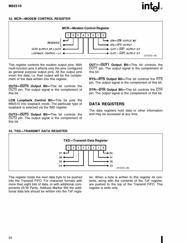
32. MCRÐMODEM CONTROL REGISTER
MCRÐModem Control Register
271072–45
This register controls the modem output pins. Withmulti-function pins it affects only the pins configuredas general purpose output pins. All the output pinsinvert the data, i.e. their output will be the comple-ment of the data written into this register.
OUT0ÐOUT0 Output BitÐThis bit controls theOUT0 pin. The output signal is the complement ofthis bit.
LCB Loopback Control BitÐThis bit puts theM82510 into loopback mode. The particular type ofloopback is selected via the IMD register.
OUT2ÐOUT2 Output BitÐThis bit controls theOUT2 pin. The output signal is the complement ofthis bit.
OUT1ÐOUT1 Output BitÐThis bit controls theOUT1 pin. The output signal is the complement ofthis bit.
RTSÐRTS Output BitÐThis bit controls the RTSpin. The output signal is the complement of this bit.
DTRÐDTR Output BitÐThis bit controls the DTRpin. The output signal is the complement of this bit.
DATA REGISTERS
The data registers hold data or other informationand may be accessed at any time.
33. TXDÐTRANSMIT DATA REGISTER
TXDÐTransmit Data Register
271072–46
This register holds the next data byte to be pushedinto the Transmit FIFO. For character formats withmore than eight bits of data, or with additional com-ponents (S/W Parity, Address Marker Bit) the addi-tional data bits should be written into the TxF regis-
ter. When a byte is written to this register its con-tents, along with the contents of the TxF register,are pushed to the top of the Transmit FIFO. Thisregister is write only.
34

M82510
34. TXFÐTRANSMIT FLAGS REGISTER
TxFÐTransmit Flags Register
271072–47
This register holds some additional components ofthe next character to be pushed into the Tx FIFO.The contents of this register are pushed into the TxFIFO with the Transmit Data register whenever theTxD register is written to by the CPU.
uLANÐuLAN Address Marker BitÐThis bit istransmitted in uLAN mode as the address markerbit.
SPÐSoftware Parity BitÐThis bit is transmitted inS/W parity mode as the character’s parity bit.
D8ÐNinth Bit of DataÐIn nine-bit character lengthmode this bit is transmitted as the MSB (D8) bit.
35. RXDÐRECEIVE DATA REGISTER
RXDÐReceive Data Register
271072–48
This register holds the earliest received character inthe Rx FIFO. The character is right justified andleading bits are zeroed. This register is loaded by the
Rx Machine with the first received character. Read-ing the register causes the next register from the RxFIFO to be loaded into RxD and RxF registers.
35

M82510
SPECIFICATIONS
NOTICE: This is a production data sheet. The specifi-cations are subject to change without notice.
*WARNING: Stressing the device beyond the ‘‘AbsoluteMaximum Ratings’’ may cause permanent damage.These are stress ratings only. Operation beyond the‘‘Operating Conditions’’ is not recommended and ex-tended exposure beyond the ‘‘Operating Conditions’’may affect device reliability.
ABSOLUTE MAXIMUM RATINGS
Case Temperature under Bias ÀÀÀb55§C to a125§CStorage Temperature ÀÀÀÀÀÀÀÀÀÀÀÀb65§ to a150§CVoltage on any Pin (w.r.t. VSS) b0.5V to VCC a0.5V
Voltage on VCC Pin (w.r.t. VSS)ÀÀÀÀÀÀb0.5V to a7V
Power DissipationÀÀÀÀÀÀÀÀÀÀÀÀÀÀÀÀÀÀÀÀÀÀÀ250 mW
Operating Conditions
Symbol Description Min Max Units
TC Case Temperature (Instant On) b55 a125 §CVCC Digital Supply Voltage 4.50 5.50 V
DC SPECIFICATIONS
DC CHARACTERISTICS (Over Specified Operating Conditions)
Symbol Parameter Notes Min Max Units
VIL Input Low Voltage (1) b0.5 0.8 V
VIH1 Input High Voltage-Cerdip (1) 2.4 VCCa0.5 V
VIH2 Input High Voltage-LCC (2) 2.6 VCCa0.5 V
VOL Output Low Voltage (2), (8) 0.45 V
VOH Output High Voltage (3), (8) 2.4 V
ILI Input Leakage Current (4) g10 mA
ILO 3-State Leakage Current (5) g10 mA
ICC Power Supply Current (6) 3.8 mA/MHz
ISTBY Standby Supply Current (9) 500 mA
IOHR RTS, DTR Strapping Current (10) 0.4 mA
IOLR RTS, DTR Strapping Current (11) 11 mA
CIN Input Capacitance (7) 10 pF
CIO I/O Capacitance (7) 10 pF
CXTAL X1, X2 Load 10 pF
NOTES:1. Does not apply to CLK/X1 pin, when configured as crystal oscillator input (X1).2. @ IOL e 2 mA.3. @ IOH e b0.4 mA.4. 0 k VIN k VCC.5. 0.45V k VOUT k (VCC b 0.45).6. VCC e 5.5V; VIL e 0.5V (max); VIH e VCC b 0.5V (min); Typical value e 2.5 mA/MHz (Not Tested); Ext 1X CLK;IOL e IOH e 0.7. Freq e 1 MHz.8. Does not apply to OUT2/X2 pin, when configured as crystal oscillator output (X2).9. Same as 7, but input clock not running.10. Applies only during hardware reset for clock configuration options. Strapping current for logic HIGH.11. Applies only during hardware reset for clock configuration. Strapping current for logic LOW.
36
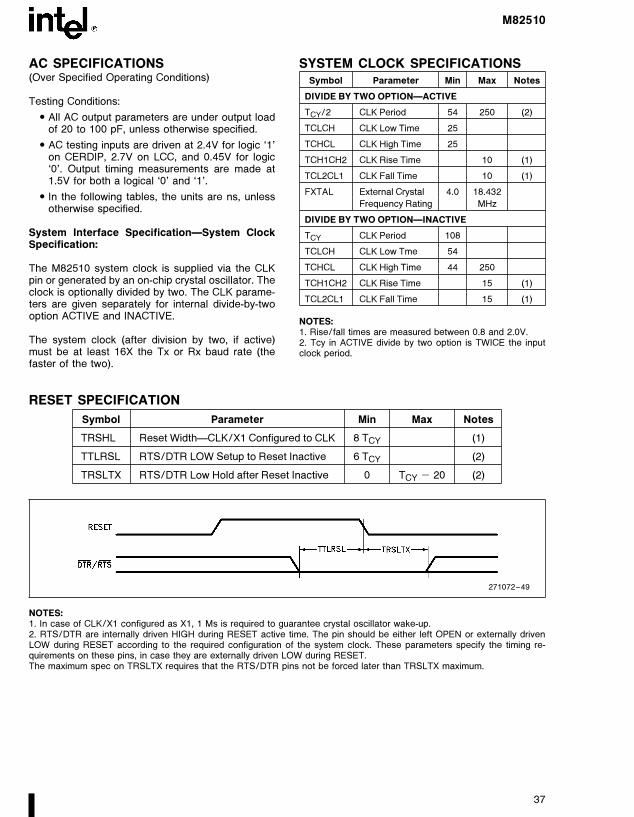
M82510
AC SPECIFICATIONS(Over Specified Operating Conditions)
Testing Conditions:
# All AC output parameters are under output loadof 20 to 100 pF, unless otherwise specified.
# AC testing inputs are driven at 2.4V for logic ‘1’on CERDIP, 2.7V on LCC, and 0.45V for logic‘0’. Output timing measurements are made at1.5V for both a logical ‘0’ and ‘1’.
# In the following tables, the units are ns, unlessotherwise specified.
System Interface SpecificationÐSystem ClockSpecification:
The M82510 system clock is supplied via the CLKpin or generated by an on-chip crystal oscillator. Theclock is optionally divided by two. The CLK parame-ters are given separately for internal divide-by-twooption ACTIVE and INACTIVE.
The system clock (after division by two, if active)must be at least 16X the Tx or Rx baud rate (thefaster of the two).
SYSTEM CLOCK SPECIFICATIONS
Symbol Parameter Min Max Notes
DIVIDE BY TWO OPTIONÐACTIVE
TCY/2 CLK Period 54 250 (2)
TCLCH CLK Low Time 25
TCHCL CLK High Time 25
TCH1CH2 CLK Rise Time 10 (1)
TCL2CL1 CLK Fall Time 10 (1)
FXTAL External Crystal 4.0 18.432
Frequency Rating MHz
DIVIDE BY TWO OPTIONÐINACTIVE
TCY CLK Period 108
TCLCH CLK Low Tme 54
TCHCL CLK High Time 44 250
TCH1CH2 CLK Rise Time 15 (1)
TCL2CL1 CLK Fall Time 15 (1)
NOTES:1. Rise/fall times are measured between 0.8 and 2.0V.2. Tcy in ACTIVE divide by two option is TWICE the inputclock period.
RESET SPECIFICATION
Symbol Parameter Min Max Notes
TRSHL Reset WidthÐCLK/X1 Configured to CLK 8 TCY (1)
TTLRSL RTS/DTR LOW Setup to Reset Inactive 6 TCY (2)
TRSLTX RTS/DTR Low Hold after Reset Inactive 0 TCY b 20 (2)
271072–49
NOTES:1. In case of CLK/X1 configured as X1, 1 Ms is required to guarantee crystal oscillator wake-up.2. RTS/DTR are internally driven HIGH during RESET active time. The pin should be either left OPEN or externally drivenLOW during RESET according to the required configuration of the system clock. These parameters specify the timing re-quirements on these pins, in case they are externally driven LOW during RESET.The maximum spec on TRSLTX requires that the RTS/DTR pins not be forced later than TRSLTX maximum.
37

M82510
READ CYCLE SPECIFICATIONS
Symbol Parameter Min Max Notes
TRLRH RD Active Width 2 Tcy a 65
TAVRL Address/CS Setup Time to RD Active 7
TRHAX Address/CS Hold Time after RD Inactive 0
TRLDV Data Out Valid Delay after RD Active 2 Tcy a 65
TCIAD Command Inactive to Active Delay Tcy a 15 (1)
TRHDZ Data Out Float Delay after RD Inactive 40
NOTE:1. Command refers to either Read or Write signals.
271072–50
WRITE CYCLE SPECIFICATION
Symbol Parameter Min Max Notes
TWLWH WR Active Width 2 Tcy a 15
TAVWL Address CS Setup Time to WR Active 7
TWHAX Address and CS Hold Time after WR 0
TDVWH Data in Setup Time to WR Inactive 90
TWHDX Data in Hold Time after WR Inactive 12
271072–51
NOTE:Many of the serial interface pins have more than one function; sometimes the different functions have different timings. Insuch a case, the timing of each function of a pin is given separately.
38

M82510
SCLK PIN SPECIFICATIONÐ16x CLOCKING MODE
Symbol Parameter Min Max Notes
TXCY SCLK Period 216
TXLXH SCLK Low Time 93
TXHXL SCLK High Time 93
TXH1XH2 SCLK Rise Time 15 (1)
TXL2XL1 SCLK Fall Time 15 (1)
NOTE:1. Rise/fall times are measured between 0.8V and 2.0V.
SCLK PIN SPECIFICATIONÐ1x CLOCK MODE
Symbol Parameter Min Max Notes
TXCY SCLK Period 3500
TXLXH SCLK Low Time 1650
TXHXL SCLK High Time 1650
TXH1XH2 SCLK Rise Time 15 (1)
TXL2XL1 SCLK Fall Time 15 (1)
NOTE:1. Rise/fall times are measured between 0.8V and 2.0V.
RXD SPECIFICATION (1x MODE)
Symbol Parameter Min Max Notes
TRPW RXD Setup Time to SCLK High 250
TRPD RXD Hold Time After SCLK High 250
271072–52
TXD SPECIFICATION (1x MODE)
Symbol Parameter Min Max Notes
TSCLKTXD TXD Valid Delay after SCLK Low Ð 170
REMOTE LOOPBACK SPECIFICATION
Symbol Parameter Min Max Notes
TRXDTXD TXD Delay after RXD Ð 170
39

M82510
Receive Logic Diagram
271072–53
Transmit Logic Diagram
271072–54
INTEL CORPORATION, 2200 Mission College Blvd., Santa Clara, CA 95052; Tel. (408) 765-8080
INTEL CORPORATION (U.K.) Ltd., Swindon, United Kingdom; Tel. (0793) 696 000
INTEL JAPAN k.k., Ibaraki-ken; Tel. 029747-8511
Printed in U.S.A./xxxx/0896/B10M/xx xx