LCD Monitor Technical Training - slot techslot-tech.com/interesting_stuff/a collection of...
28
LCD Monitor Technical Training 1/28 * Model ; Analog M series LCD monitor - L1510SM - L1710SM - L1910SM - L1515SM - L1715SM - L1520BM - L1720BM - L1920BM - L1530SM - L1730SM - L1930SM
Transcript of LCD Monitor Technical Training - slot techslot-tech.com/interesting_stuff/a collection of...
LCD Monitor Technical Training
� 1/28
* Model; Analog M series LCD monitor
- L1510SM- L1710SM- L1910SM- L1515SM - L1715SM - L1520BM- L1720BM- L1920BM- L1530SM- L1730SM- L1930SM
Content
� 2/28
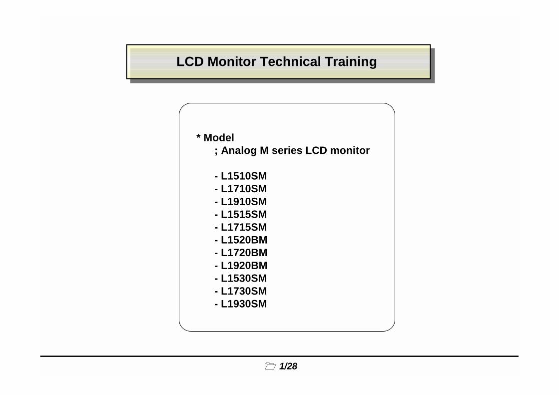
1. I/F Circuit operation Description1) Block diagram2) Signal Input block3) Supply Voltage regulation block4) Scaler Block5) Micro controller Block
2. LIPS block operation description 1) Block diagram2) SMPS Block3) Inverter Block
3. Appendix ; Operation principle of LCD Monitor
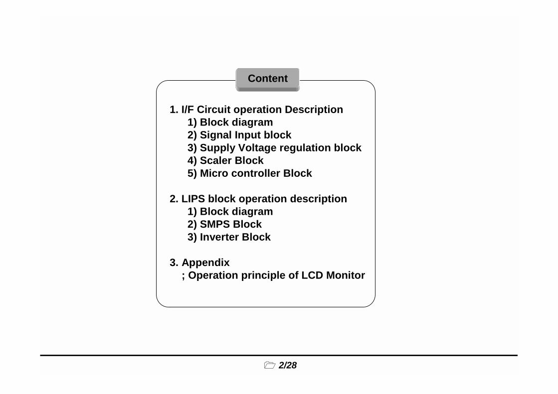
1.1. Block diagram
� 3/28
D-SUB
MST9111Aincluding
(ADC /LVDS )
MCU
LCD Module
R,G,B differential
������������� ���� � �������������
SCL
SDA
LIPS
5V
AVDD 3.3VDVDD 3.3V
5V
AC Input
AVDD 2.5VDVDD 2.5V
3.3VReg.
AVDD3.3VDVDD3.3V
2.5VReg.
AVDD2.5VDVDD2.5V
5V 5V
12VR,G,B, H/V Sync
5V
1. I/F Circuit operation Description
� 4/28
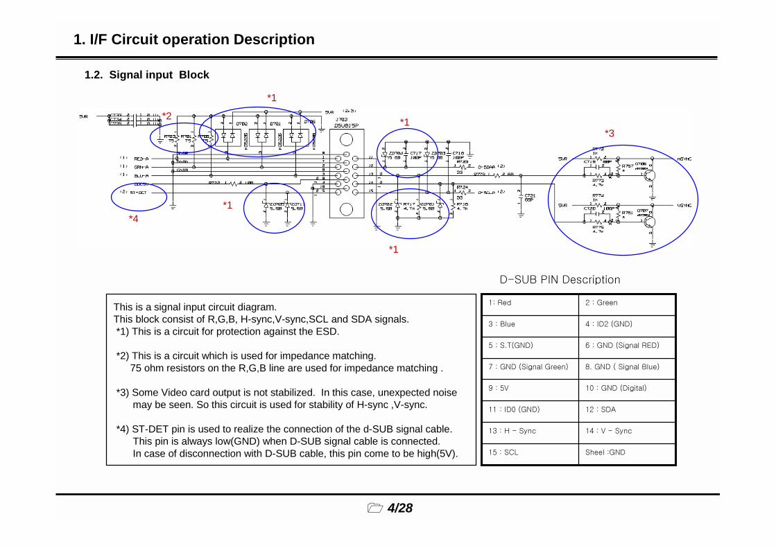
1.2. Signal input Block
This is a signal input circuit diagram.This block consist of R,G,B, H-sync,V-sync,SCL and SDA signals.*1) This is a circuit for protection against the ESD.
*2) This is a circuit which is used for impedance matching.75 ohm resistors on the R,G,B line are used for impedance matching .
*3) Some Video card output is not stabilized. In this case, unexpected noisemay be seen. So this circuit is used for stability of H-sync ,V-sync.
*4) ST-DET pin is used to realize the connection of the d-SUB signal cable.This pin is always low(GND) when D-SUB signal cable is connected.In case of disconnection with D-SUB cable, this pin come to be high(5V). ���������������
������� ����������� ����
����������������
��������������� �����
!"�������������#�$��%���������������&����
'��������������()������"*����
���������������#�$�
�����&�����(�+
*1
*1
*1
*1
*2*3
*4
������������ ������
1. I/F Circuit operation Description
� 5/28
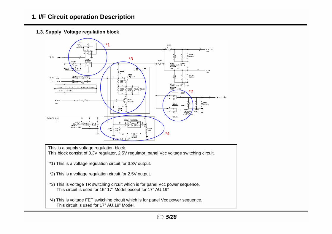
1.3. Supply Voltage regulation block
This is a supply voltage regulation block.This block consist of 3.3V regulator, 2.5V regulator, panel Vcc voltage switching circuit.
*1) This is a voltage regulation circuit for 3.3V output.
*2) This is a voltage regulation circuit for 2.5V output.
*3) This is voltage TR switching circuit which is for panel Vcc power sequence. This circuit is used for 15” 17” Model except for 17” AU,19”
*4) This is voltage FET switching circuit which is for panel Vcc power sequence. This circuit is used for 17” AU,19” Model.
*1
*2
*3
*4
1. I/F Circuit operation Description
� 6/28
1.4. Scaler block
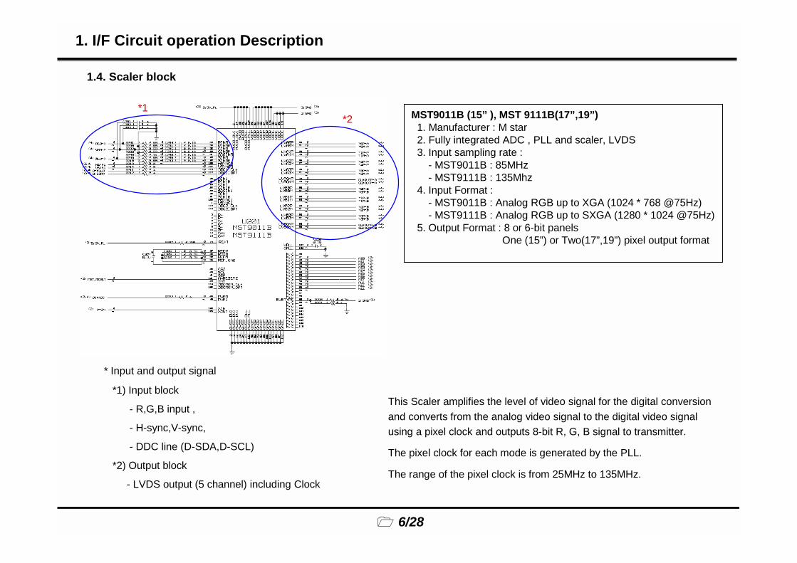
MST9011B (15” ), MST 9111B(17”,19”)1. Manufacturer : M star2. Fully integrated ADC , PLL and scaler, LVDS3. Input sampling rate :
- MST9011B : 85MHz - MST9111B : 135Mhz
4. Input Format : - MST9011B : Analog RGB up to XGA (1024 * 768 @75Hz)- MST9111B : Analog RGB up to SXGA (1280 * 1024 @75Hz)
5. Output Format : 8 or 6-bit panelsOne (15”) or Two(17”,19”) pixel output format
*1*2
* Input and output signal
*1) Input block
- R,G,B input ,
- H-sync,V-sync,
- DDC line (D-SDA,D-SCL)
*2) Output block
- LVDS output (5 channel) including Clock
This Scaler amplifies the level of video signal for the digital conversion and converts from the analog video signal to the digital video signal using a pixel clock and outputs 8-bit R, G, B signal to transmitter.
The pixel clock for each mode is generated by the PLL.
The range of the pixel clock is from 25MHz to 135MHz.
1. I/F Circuit operation Description

� 7/28
1.5. micro-controller block
This block consists of u-controller, EEPROM IC which stores control data, and Reset IC
*1) U-controllerThe u-controller distinguishes polarity and frequency of the H/V sync are supplied from signal cable.And u-controller control “Inverter on”, “ LCD power on”, “Lamp current Adjust” and communication with scaler.
*2) EEPROMThe controlled data of each modes is stored in EEPROM.
*3) Reset blockThe reset of the u-controller is active “High”KIA7042 reset IC’s output is low until 5V come to be over 4.2V so that u-controller can have stable reset operation.
*1
*2
*3
1.I/F Circuit operation Description

2.1. Block diagram
2. LIPS block operation description
� 8/28

2.2. SMPS Block
2.LIPS block operation description
*3
*1 *2 *5
*6
*4
� 9/28
2.2. SMPS Block
2.LIPS block operation description
This block is SMPS block.
*1) EMI componentThis block construct Low pass filter for.
*2) Input rectifier and smoothing filterThis block change AC input voltage to high DC voltage
*3) PWM control circuitControl PWM oscillator frequency and drive switching MOSFET.
*4) Energy transfer TransformerChange high voltage on primary side to low voltage on secondary side and meet the output voltage spec.
*5) Output rectifier and filter- Through rectifier diode, get the DC voltage 12V,5V .- Construct filter to get more approach DC voltage.
*6) Feedback circuitConstruct feedback circuit to control U101 wavy duty.
� 10/28
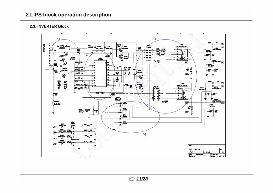
2.3. INVERTER Block
2.LIPS block operation description
*1
*2
*3
*4
� 11/28
2.3. Inverter Block
2.LIPS block operation description
This block is Inverter block.
*1) Reset circuitThis block is for voltage detecting. When input 5V is less than 5VDC, U302 KIA7042 will shut down U301(OZ960). U301 (OZ960) will be reset if the voltage is recovered 5VDC.
*2) PWM controllerU301 (OZ960) is the PWM output controller to drive CCFL .
*3) Drive networkDual MOSFET for switch direct network to drive transformer.
*4) Feedback and OVP circuit.Detect kick off voltage from transformer and transfer this feedback voltage to pin 2 of U301.If the feedback voltage is over 2V, U301(OZ960) will be shut down.
� 12/28
� 13/28
1) LCD Monitor Block diagram2) Video signal Timing 3) Analog to Digital Converter 4) ADC Calibration5) Pixel sampling6) Output TTL Timing7) LVDS8) Power sequence for panel
Appendix
Operation principle of LCD Monitor(Analog)

1. LCD Monitor Block diagram
� 14/28
ScalerA/DConverterPre-Amp.
ClockGenerator
R/G/B R/G/B
Micro-Controller
H/V Sync
Digital
H Sync
H SyncClock
LVDSTX
LCD
Module
R/G/B24 bit
Analog
R/G/B24 bit
Dclk/H/V/DE
Inverter
Signal Flow
Appendix
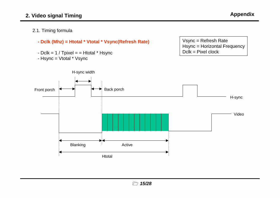
2.1. Timing formula
- Dclk (Mhz) = Htotal * Vtotal * Vsync(Refresh Rate)
- Dclk = 1 / Tpixel = = Htotal * Hsync - Hsync = Vtotal * Vsync
Vsync = Refresh RateHsync = Horizontal FrequencyDclk = Pixel clock
Front porch
Video
H-sync
H-sync width
Back porch
Blanking Active
Htotal
2. Video signal Timing
� 15/28
Appendix
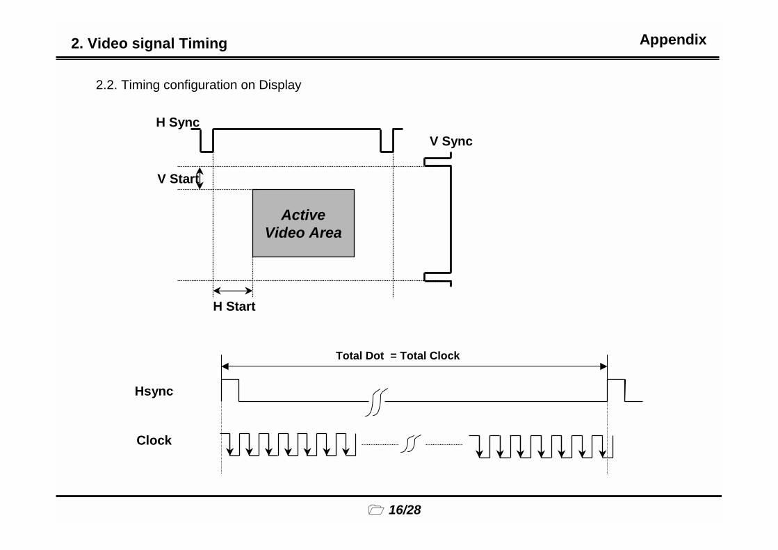
2. Video signal Timing
ActiveVideo Area
H SyncV Sync
V Start
H Start
Hsync
Total Dot = Total Clock
Clock
2.2. Timing configuration on Display
� 16/28
Appendix
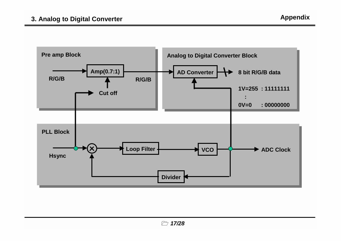
3. Analog to Digital Converter
Divider
Loop Filter VCOHsync
ADC Clock
PLL Block
Amp(0.7:1)R/G/B
Pre amp Block
Cut off
AD ConverterR/G/B
Analog to Digital Converter Block
8 bit R/G/B data
1V=255 : 11111111:
0V=0 : 00000000
� 17/28
Appendix
4. ADC Calibration
4.1. ADC Calibration Procedure
� 18/28
������������������� �����������������������������������������
��������������������������� �������������������� ��������
�������������������������������� ����������������������������������������� !"�������
#��!�$%��������������&��������������������&���'��&�������(������������
��������(����������������� ��
�����������!�$%�������������������������'�����������������������������)
'�������������&�������������������
��������������������������&�����'������������
Appendix
4. ADC Calibration
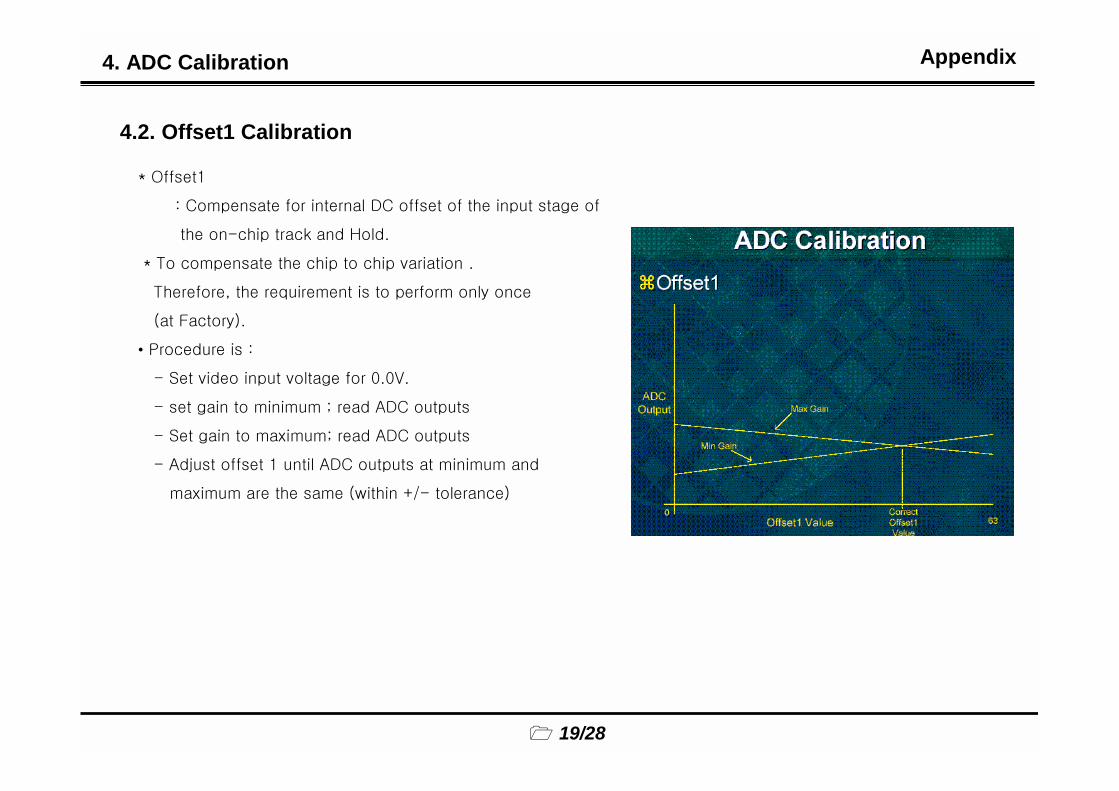
4.2. Offset1 Calibration
� 19/28
*�������
+���������������������� ��������������������&��
�����,���������������-���
*����������������������������������������
�������)�������.����������������������/����
0��������/1�
• 2�����������+
, �������������������&����3�34�
, ����&��������������5������� ��������
, ����&��������(����5������� ��������
, ��6����������������� ������������������������
��(������������������0'������78, ��������1
Appendix
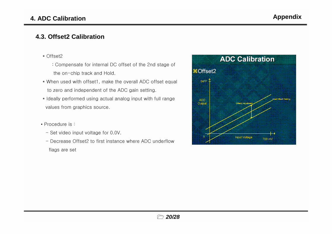
4.3. Offset2 Calibration
4. ADC Calibration
� 20/28
*������
+���������������������� ������������������&���
�����,���������������-���
*�9���������'��������)������������������ �������.����
��:������������������������� ��&����������&��
*�$�����/�������������&������������&�������'�����������&��
����������&��������������
• 2�����������+
, �������������������&����3�34�
, ������������������������������'������ ��������'�
��&���������
Appendix
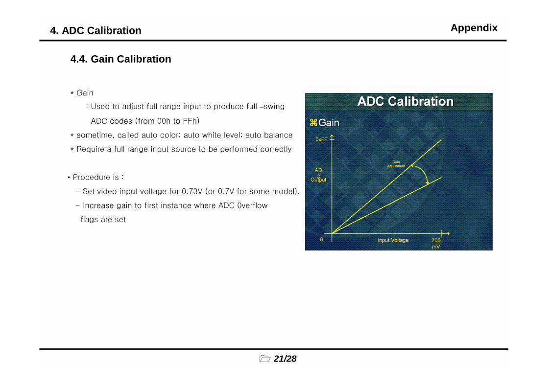
4.4. Gain Calibration
4. ADC Calibration
� 21/28
*�!����
+�;��������6�����������&���������������������–�'��&
� �������0���33�������1�
*��������)���������������5�����'����������5��������������
*� �.��������������&����������������������������������/�
• 2�����������+
, �������������������&����3�<#4�0��3�<4�����������1�
, $��������&��������������������'������ ��3����'�
��&���������
Appendix
4.5. Effect of incorrect ADC calibration
4. ADC Calibration
� 22/28
*�$�� ���������������������������������/)��������'��&��������������������&�����������������������
, ����������“9����”
� ���������������������������'�����������������’������������������
, “;������” ������
� �����������������������������������������’������������������������������’�����������&��
, �����������������������
Appendix
5. Pixel sampling
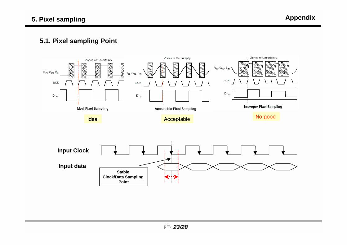
5.1. Pixel sampling Point
�������������������� ���������������������������������� ������ ������ ������ ����
Input Clock
Input dataStable
Clock/Data Sampling Point
� 23/28
Appendix

5. Pixel sampling
5.2. How to find best pixel sampling point
���� ���� �
��������
��������
��������
��������
����������������
�������� ����������������
� �
�
"
� 24/28
� � � � ��� �� ����� ������������� �� ����� ������������� �� ����� ������������� �� ����� ����������
+����������������6�������)�
“�������(�����������” ���������������
������(������������&�������������������������
��������∑ �������
*�������������������������������/����'�����������
Appendix
������������������������ ������������������������������������� ��������������� ������������������������������������� ��������������� ������������������������������������� ��������������� ������������������������������������� �������
����
�����
��� ��
�� ��
� ������������������� ���������������������������������������������
� ����� ����������
�� ������ ���������������������������������������
! ��" �#��"$�#�� ����������
�� ���" �#��"$�#�� ����������������������������������������
% ��" �#��"$�#�� ���������
�� ���" �#��"$�#�� ���������������������������������������
������
������
������������
������
������
������
������
������
������
������� �����
������ ����
���������������
������
�������
������
������
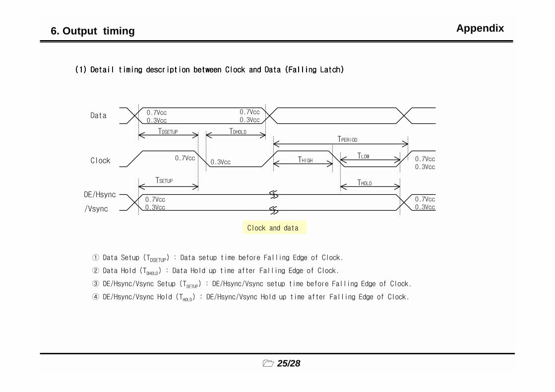
6. Output timing
� 25/28
Appendix

���������������������������� �������������������������� �������������������� �������������������������� �������������������� �������������������������� �������������������� �������������������������� ��������
� $��������������&���'�
� $���������#���(���'�
! $��������)����&���'�
% $�������������� �*���+��,����-�$��������)����&���'�-�$��������������&���'
. ���/������������&���'�
0 ���/�������#���(���'��
1 ���/������)����&���'�
2 ���/������������ �*���+��&�3���-� ���/������)����&���'�-� ���/������������&���'
4 *���+��,���� �*���+��,��������
5 *���+������� �*���+��&�3�������
$�#��
��
�#��
� � !
%
4
2 5“*”
“*” )�����������
��
�#��
�����
. 0 1
6������#�����������������
6. Output timing
� 26/28
Appendix
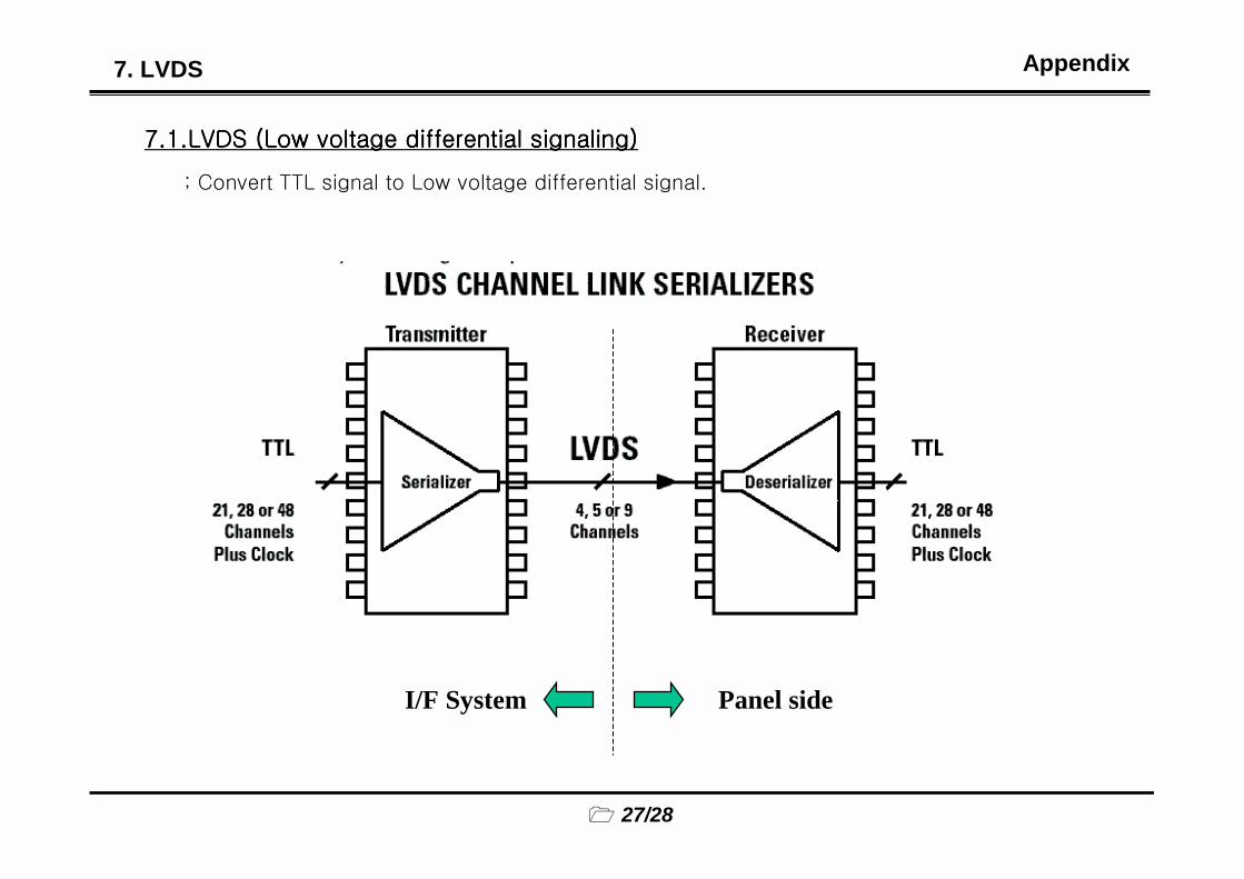
7. LVDS
������������������������� ���������������� ������ ������������� ���������������� ������ ������������� ���������������� ������ ������������� ���������������� ������ ����
������������ ������������������� ������ ���� �����
� 27/28
Panel sideI/F System
Appendix
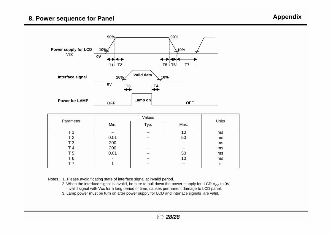
8. Power sequence for Panel
� 28/28
Notes : 1. Please avoid floating state of interface signal at invalid period.2. When the interface signal is invalid, be sure to pull down the power supply for LCD VCC to 0V.
Invalid signal with Vcc for a long period of time, causes permanent damage to LCD panel.3. Lamp power must be turn on after power supply for LCD and interface signals are valid.
Parameter UnitsMin.
Values
Typ. Max.
T 1T 2T 3T 4T 5T 6T 7
msmsmsmsmsmss
�
0.012002000.01
-1
�
�
�
�
�
�
�
1050�
�
5010�
10%
90% 90%
10%
T1 T2 T5 T6 T7
T3 T4
Valid data
Lamp on
0V
OFF OFF
Power supply for LCDVcc
Interface signal
Power for LAMP
10% 10%
0V
Appendix