Introduction to CMOS Pixel Sensors
22
- EDIT School — CERN, February 2011 Introduction to CMOS Pixel Sensors Marc Winter (IPHC-Strasbourg) (next week : J ´ er ˆ ome Baudot / IPHC-Strasbourg) more information on IPHC Web site: http://www.iphc.cnrs.fr/-CMOS-ILC-.html OUTLINE • Main features of CMOS pixel sensors motivation principle: sensing & read-out limitations hit characteristics • Achieved performances means of evaluation beam test characterisation sources of performance deterioration • Applications system integration aspects subatomic physics apparatus • Outlook 2D sensors 3D sensors • Summary , –1–
-
Upload
truongnhan -
Category
Documents
-
view
238 -
download
1
Transcript of Introduction to CMOS Pixel Sensors

- EDIT School — CERN, February 2011
Introduction to CMOS Pixel SensorsMarc Winter (IPHC-Strasbourg)
(next week : Jerome Baudot / IPHC-Strasbourg)B more information on IPHC Web site: http://www.iphc.cnrs.fr/-CMOS-ILC-.html
OUTLINE
• Main features of CMOS pixel sensors
B motivation B principle: sensing & read-out B limitations B hit characteristics
• Achieved performances
B means of evaluation B beam test characterisation B sources of performance deterioration
• Applications
B system integration aspects B subatomic physics apparatus
• Outlook
B 2D sensors B 3D sensors
• Summary
, –1–

- The Quadrature of the Vertex Detector
Power Consumption
• CMOS pixel sensors offer the perspective of ”combining the extremes” (ultimately !)
• Several labs develop CMOS pixel sensors : Italy (INFN, Univ.), UK (RAL), CERN, France (IPHC, Saclay), USA, ...
• Several experiments chosed/envisage CMOS pixel sensors : STAR (construct), CBM (devt),
ALICE (option), SuperB (option), ILC (option), ...
, –2–

- CMOS Technology
• C.M.O.S. ≡ Complementary Metal-Oxide-Semiconductor
• CMOS pixel sensors exploit the fabrication processes
used in industry for mass production of integrated circuits :
> micro-processors, micro-controler, RAM, ...
> cell phones, lap tops, cars, ...
• CMOS fabrication mode :
> µcircuit lithography on a substrate
> proceeds through reticules (2x2 cm2) organised in wafers
, –3–

- Main Features of CMOS Sensors
• P-type low-resistivity Si hosting n-type ”charge collecto rs”
• signal created in epitaxial layer (low doping):
Q ∼ 80 e-h / µm 7→ signal . 1000 e−
• charge sensing through n-well/p-epi junction
• excess carriers propagate (thermally) to diode
with help of reflection on boundaries
with p-well and substrate (high doping)
• Prominent advantages of CMOS sensors:
granularity: pixels of . 10×10 µm2 V high spatial resolution
low mat. budget: sensitive volume ∼ 10 - 20 µm V total thickness . 50 µm
signal processing µcircuits integrated in the sensors V compacity, high data throughput, flexibility, etc.
other attractive aspects: T room operation, cost, multi-project run frequency, industrial reliability,
industrial technology devts & evolution, etc.
B B B Thinning down to ∼ 30 µm permitted
, –4–

- Basic Read-Out Architecture
, –5–

- CMOS Pixel Sensors: Read-Out Architectures
• Signal sensing and read-out are decoupled :
> signal sensing (charge collection) is continuous (no dead time)
V signal read-out may be performed in various ways, independently of charge collection
• Signal processing alternatives :
> self-triggered : only fired pixels are (randomly) read-out ≡ hybrid pixels
> rolling shutter (less power consumption) : read-out of all pixels,
followed by sparsification outside of sensitive area BBBB
> snap-shot : requires 2 consecutive read-outs,
with 1 used for average noise subtraction
(rather suited to light imaging due to ∼ 50 % dead time)
• Signal transfer alternatives :
> continuous : permanent output to outside world
> intermittent : signal stored on chip until read-out sign is provided
→ event based trigger or beam-time structure (ILC) BBB
, –6–
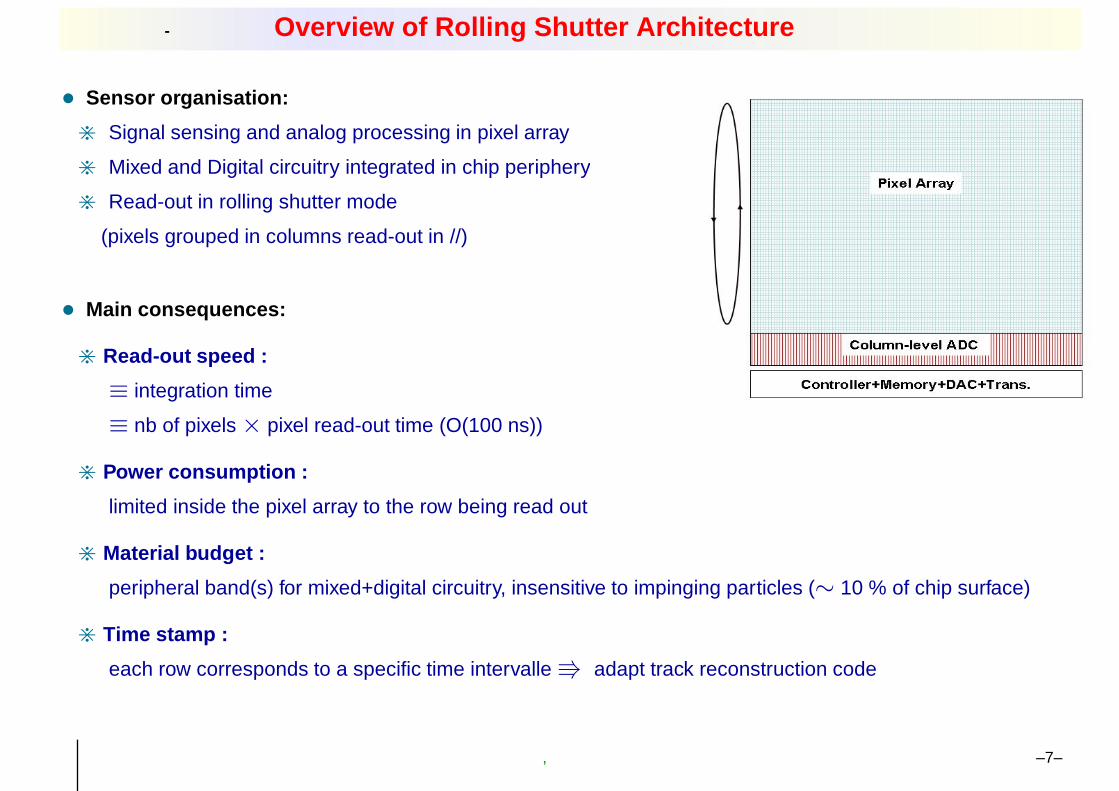
- Overview of Rolling Shutter Architecture
• Sensor organisation:
> Signal sensing and analog processing in pixel array
> Mixed and Digital circuitry integrated in chip periphery
> Read-out in rolling shutter mode
(pixels grouped in columns read-out in //)
• Main consequences:
> Read-out speed :
≡ integration time
≡ nb of pixels × pixel read-out time (O(100 ns))
> Power consumption :
limited inside the pixel array to the row being read out
> Material budget :
peripheral band(s) for mixed+digital circuitry, insensitive to impinging particles (∼ 10 % of chip surface)
> Time stamp :
each row corresponds to a specific time intervalle V adapt track reconstruction code
, –7–

- Signal Sensing & Processing Architectures
• Main sensing and read-out micro-circuit elements
> in-pixel conversion of charge into electrical signal (e.g. voltage) with average noise subtraction
> signal discrimination (in perspective of zero-suppression)
> discriminator output encoding (sparsification with charge encoding)
> data transmission logic connection with the outside world
• In-pixel µcircuitry :
basic read-out pre-amp + <noise> subtraction pre-amp + shaper + discriminator
data : outside chip chip periphery inside pixelreduction
, –8–

- Limitations of the Technology
• Very thin sensitive volume
V impact on signal magnitude (mV !)
V very low noise FEE required
• Sensitive volume almost undepleted
V impact on radiation tolerance & speed
B tendency : high-resistivity epitaxial layer V improved radiation tolerance
• Commercial fabrication
V fabrication parametres (doping profile epitaxial layer, number of metal layers, etc.)
not optimal for charged particle detection :
> real potential of CMOS pixel sensors not exploited
> choice of process often driven by epitaxial layer characteristics,
at the expense of the FEE circuitry parametres (feature size, nb of Metal Layers)
• Use of P-MOS transistors inside pixel array restricted in mo st processes
V limited signal processing functionnalities inside pixels (most performed on sensor periphery)
B tendency : buried n-well techno. V allows use of P-MOS transistors (watch charge coll. eff. !)
, –9–

- Hit Characteristics
• Standard processes : charges diffuse thermally
> . 103 e− shared among ∼ 10-15 pixels per cluster
> typically . 200/300 e− on seed pixel
• High-resistivity epitaxial layer : larger charge sensing v olume
> less diffusion V less pixels/cluster
> larger charge collected/pixel V higher SNR
Cluster charge (electrons)
0 1000 2000 3000 4000 5000 6000 7000
Eve
nts
0
20
40
60
80
100
120
140
Total cluster charge (5x5 pixels)
Landau fit
Threshold (mV)2 4 6 8 10 12 14
# pi
xels
in h
it
1
2
3
4
5
6
Pixel multiplicity vs Threshold
PRELIMIN
ARYMi-26 standard
Mi-26 standard 2009
Mi-26 HR-10
Mi-26 HR-15
Mi-26 HR-20
Pixel multiplicity vs Threshold
, –10–

- Sensor Noise: Sources, Reduction Strategies
• Main Sources :
> in pixel : sensing diode capacitance BBB
> in pixel : leakage current collected by sensing diode BB
> outside pixel : signal processing micro-circuits
• Tricks to minimise the noise :
> maximal amplification inside pixel
V minimises the impact of the noise BBB
of the signal processing micro-circuits
> operate chip with short integration time
V minimises the integrated leakage current
> operate chip at low temperature BBB
V minimises the thermal noise
, –11–

- M.I.P. Detection Performance Evaluation
• Laboratory :
> test steering & read-out functionalities (e.g. pattern generator)
> evaluate charge collection efficiency & noise (55Fe)
> assess charge-to-voltage conversion factor (55Fe)
> estimate ”m.i.p.” detection efficiency with β (106Ru)
• M.I.P. beam :
> typically ∼ 100 GeV/c π− at CERN-SPS
V minimise multiple scattering
> install chip to test inside beam telescope (EUDET BT)
> determine :
detection efficiency (and SNR)
fake hit rate (and noise)
single point resolution
, –12–

- CMOS Pixel Sensors: State of the Art
courtesy of Ch. Hu-Guo / TWEPP-2010
, –13–

- M.I.P. Detection Efficiency & Fake Hit Rate
• Motivation : find a sensor working point
with high detection efficiency and marginal
contamination by noise fluctuations (fake hits)
• Detection efficiency
> fraction of tracks reconstructed in telescope
which are also reconstructed in the sensor
> study as function of discriminator threshold
> a high threshold may harm detection efficiency
• Fake hit rate
> fraction of noise fluctuations which pass the discriminator threshold
> study as a function of discriminator threshold
> a high threshold is best to keep fake rate marginal
(typically . 10−3/−4)
Fake hit rate-810 -710 -610 -510 -410 -310
Effic
ienc
y (%
)
94
95
96
97
98
99
100
101
Efficiency vs Fake hit rate
Threshold (mV)3 4 5 6 7 8 9 10 11
Effic
ienc
y (%
)
94
95
96
97
98
99
100
101
Aver
age
fake
hit
rate
/pix
el/e
vent
-810
-710
-610
-510
-410
-310
-210
-110
1
Mi-26 HR-10
, –14–

- Spatial Resolution
• Compare position of impact on sensor surface predicted
with BT to hit reconstructed with sensor under test:
clusters reconstructed with eta-function,
exploiting charge sharing between pixels
• Impact of pixel pitch (analog output): BBB
σsp ∼ 1 µm (10 µm pitch) . 3 µm (40 µm pitch)
• Impact of charge encoding resolution : BBB
B ex. of 20 µm pitch V σdigisp = pitch/
√12 ∼ 5.7 µm
Nb of bits 12 3-4 1
Data measured reprocessed measured
σsp . 1.5µm . 2µm .3.5µm
pitch (microns)
5 10 15 20 25 30 35 40 45
Res
olut
ion
(mic
rons
)
0.5
1
1.5
2
2.5
3
3.5
Mimosa resolution vs pitchMimosa resolution vs pitch
Threshold (S/N)4 5 6 7 8 9 10 11 12
m)
µR
esol
utio
n (
2
2.5
3
3.5
4
4.5
5
Resolution vs Threshold
S11 (CAS)
S12 (CAS)
S13 (CS)
S14 (CS)
Resolution vs Threshold
Threshold (S/N)4 5 6 7 8 9 10 11 12
m)
µR
esol
utio
n (
2
2.5
3
3.5
4
4.5
5
Resolution vs Threshold
S6 (CAS)
S7 (CS)
S8 (CAS-L)
S9 (CAS-S)
S10 (CAS)
Resolution vs Threshold
18.4 µm 20.7 µm
, –15–

- Radiation Tolerance
• Introductory remarks :
> still evolving (csq of CMOS industry process param. evolution)
> CMOS technology expected to tolerate high ionising radiation
doses (>> 10 MRad), in particular at < 0C and short tinteg
> main a priori concern : NON-ionising radiation
(in absence of thick depleted sensitive volume)
• Influence of pixel pitch : BBB
> fig: all measts done with low resistivity epitaxial layer, but 1
V high density sensing diodes (≡ small pitch)
improves non-ionising radiation tolerance
• Influence of epitaxial layer resistivity :
> ex: 400 Ω · cm & O(1)V depletion voltage BBB
> trend : & 1 kΩ · cm & >> 10 V
V tolerance to & 1014−15 neq /cm2 not excluded
discriminator threshold (mV)4 5 6 7 8 9 10 11
: ef
ficie
ncy
(%)
94
95
96
97
98
99
100
101
m)
µo
: res
olut
ion
(
0
1
2
3
4
5
6
: av
erag
e fa
ke h
it ra
te/p
ixel
/eve
nt∆
-710
-610
-510
-410
-310
-210Mi26 HR-15 non-irradiated
° fluence at 0 2/cmeq n13Mi26 HR-15 after 1.10
, –16–

- Sensor Integration in Ultra Light Devices
• ”Useful” sensor thickness . 30 µm V opens new possibilities w.r.t. thicker sensors
B coarse thickness of sensors (e.g. EUDET BT) is 50 µm
• STAR-PXL ladder (room temperature, single-end supported):
> total material budget ' 0.37 % X0 :
50 µm thin sensors ' 0.05 % X0
flexible cable ' 0.07 % X0
mechanical support ' 0.2 % X0
adhesive, etc. ' 0.05 % X0
• Double-sided ladders with ∼ 0.2-0.3 % X0 :
V manifold bonus : compactness, alignment, redundancy,
pointing accuracy (shallow angle), fake hit rejection, etc.
• Unsupported & flexible ladders with . 0.15 % X0
V 30 µm thin CMOS sensors mounted on thin cable
& embedded in thin polyimide suited to beam pipe ?
, –17–

- Applications in Subatomic Physics
• Beam telescopes :
> EUDET (FP-6 / 2006-2010) : 6 planes with 1×2 cm2 sensors
> AIDA (FP-7 / 2011-2015) : ≥ 3 planes with 5×5 cm2 sensors
• Vertex detectors :
> STAR-PXL at RHIC : 2 layers
> CBM-MVD at FAIR/GSI : 2-3 stations
> option for ALICE-ITS at LHC: Layer-0 + ...
> option for Vertex detector at SuperB fact. : L0 + ...
> option for ILD-VTX at ILC : 3 double-layers
• Trackers (”large pitch”) :
> BES-III at BEPC
> in general : trackers surrounding vertex detectors
• EM calorimetres : SiW calorimetre
, –18–
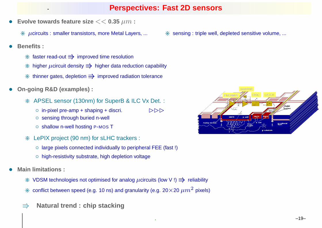
- Perspectives: Fast 2D sensors
• Evolve towards feature size << 0.35 µm :
> µcircuits : smaller transistors, more Metal Layers, ... > sensing : triple well, depleted sensitive volume, ...
• Benefits :
> faster read-out V improved time resolution
> higher µcircuit density V higher data reduction capability
> thinner gates, depletion V improved radiation tolerance
• On-going R&D (examples) :
> APSEL sensor (130nm) for SuperB & ILC Vx Det. :
in-pixel pre-amp + shaping + discri. BBB sensing through buried n-well
shallow n-well hosting P-MOS T
> LePIX project (90 nm) for sLHC trackers :
large pixels connected individually to peripheral FEE (fast !)
high-resistivity substrate, high depletion voltage
• Main limitations :
> VDSM technologies not optimised for analog µcircuits (low V !) V reliability
> conflict between speed (e.g. 10 ns) and granularity (e.g. 20×20 µm2 pixels)
V Natural trend : chip stacking
, –19–

- Using 3DIT to reach Ultimate CMOS Sensor Performances
• 3D Integration Technologies allow integrating high density signal processing µcircuits inside small pixels
by stacking (∼ 10 µm) thin tiers interconnected at pixel level
• 3DIT are expected to be particularly beneficial for CMOS sens ors :
> combine different fab. processes V chose best one for each tier/functionnality
> alleviate constraints on peripheral circuitry and on transistor type inside pixel, etc.
• Split signal collection and processing functionnalities :
> Tier-1: charge sensing
> Tier-2: analog-mixed µcircuits
> Tier-3: digital µcircuits
• The path to nominal exploitation of CMOS pixel potential :
> fully depleted 10-20 µm thick epitaxy V . 5 ns collection time, rad. hardness > Hybrid Pix. Sensors ???
> FEE with ≤ 10 ns time resolution solution for CLIC & HL-LHC specifications ???
• 3DIC ≡ consortium coordinated by FermiLab has already produced 1s t generation of chips
, –20–

- SUMMARY
• CMOS sensor technology is becoming mature for high performa nce vertexing
> most relevant for specifications governed by granularity, material budget, power consumption, ...
> excellent performance record with beam telescopes (e.g. EUDET project)
> 1st vertex detector experience will be gained with STAR-PXL, starting data taking in ∼ 2 years
> new generation of sensors under development for experiments > 2015 (including trackers & calo.)
• Technology full potential still far from being exploited
(despite improvement due to high-resistivity epitaxial la yer processes)
• Evolution of industry opens the door to 2 ”natural” steps
towards the ”ultimate” performances of the technology :
> fast 2D sensors based on VDSM CMOS technologies may allow for . O(1) µs, >> 10 MRad
> 3D chips are expected to ”exhaust” the technology potential, but there is a long way to go
V may lead to fast & rad. hard devices suited to sLHC & CLIC
, –21–

- Calibration of Charge-to-Voltage Conversion Factor
• Goal : establish a well defined correspondence between the measure d sensor output voltages
and the amplitude of the charge collected by each diode
• Mean : use radioactive sources emitting particles with adapted and well defined energy
• Ex: 55Fe
> emits X-Rays with 5.9 keV (∼ 90%) or 6.49 keV (∼ 10%)
> X-Rays interact with Si atoms through photo-electric effect
V the ejected p.e. carries ∼ 100% of the X-Ray energy
(e− binding energy ...)
> the p.e. creates eh pairs at the expense of ∼ 3.6 eV per pair
V 5900/3.6 ' 1640 eh pairs (6490/3.6 ' 1800 eh)
• Calibration with 55Fe X-Rays
> a few % of X-Rays impinge sensor near sensing diode
V nearly all e− created get collected by nearby sensing diode > the charge distribution observed on the ADC scale exhibits 2 peaks
, –22–