CMOS digital pixel sensors: technology and...
14
CMOS digital pixel sensors: technology and applications Orit Skorka and Dileepan Joseph Electrical and Computer Engineering, University of Alberta, Edmonton, AB, Canada ABSTRACT CMOS active pixel sensor technology, which is widely used these days for digital imaging, is based on analog pixels. Transition to digital pixel sensors can boost signal-to-noise ratios and enhance image quality, but can increase pixel area to dimensions that are impractical for the high-volume market of consumer electronic devices. There are two main approaches to digital pixel design. The first uses digitization methods that largely rely on photodetector properties and so are unique to imaging. The second is based on adaptation of a classical analog-to-digital converter (ADC) for in-pixel data conversion. Imaging systems for medical, industrial, and security applications are emerging lower-volume markets that can benefit from these in-pixel ADCs. With these applications, larger pixels are typically acceptable, and imaging may be done in invisible spectral bands. Keywords: CMOS image sensors, market trends, imaging applications, electromagnetic spectrum, pixel pitch, digital pixel sensors, analog-to-digital converters, photodetectors. 1. INTRODUCTION The image sensor market was traditionally dominated by charge-coupled device (CCD) technology. Ease of on-chip integration, higher frame rate, lower power consumption, and lower manufacturing costs pushed com- plementary metal-oxide-semiconductor (CMOS) active pixel sensor (APS) technology to catch up with CCDs. This trend is especially prominent in the high-volume consumer electronics market. Furthermore, the difference in image quality, which gave advantage to CCDs in early days, has substantially reduced over the years. When using either CCD or CMOS APS technology, electronic image sensors are based on analog pixels. With CCD sensors, data conversion is done at board level, and with CMOS APS ones, data conversion is done at either chip or column level. Because digital data is more immune to noise, transition to digital pixels can enhance performance on signal and noise figures of merit. In particular, digital pixels enable higher signal-to-noise-and- distortion ratios (SNDRs), lower dark limits (DLs), and wider dynamic ranges (DRs). SNDR is directly related to image quality, DL manifests in performance under dim lighting, and DR indicates maximal range of brightness that can be properly captured in a single frame. With digital pixel sensor (DPS) technology, data conversion is done at pixel level, where each pixel outputs a digital signal. Digital pixels are larger than analog ones because they contain more circuit blocks and more transistors per pixel. These days, the highest volume of the image sensor market is based on consumer electronics applications that favor small pixels and high resolution arrays. Many DPS designs are currently unsuitable for this market segment. However, there are medical, surveillance, industrial, and automotive imaging applications that can accept large pixels and benefit from digital pixels. These are low-volume growing markets, where imaging is sometimes done in invisible bands of the spectrum. There are many approaches to DPS design, where specific application requirements make some preferred over others. In this review paper, Section 2 analyzes the market of CMOS image sensors, focusing on diversification into invisible spectral bands. Section 3 compares and contrasts various digital pixel architectures in the literature. Main points are summarized in the conclusion section. Please address correspondence to [email protected]. Invited Paper Nanosensors, Biosensors, and Info-Tech Sensors and Systems 2014, edited by Vijay K. Varadan, Proc. of SPIE Vol. 9060, 90600G · © 2014 SPIE · CCC code: 0277-786X/14/$18 · doi: 10.1117/12.2044808 Proc. of SPIE Vol. 9060 90600G-1
Transcript of CMOS digital pixel sensors: technology and...

CMOS digital pixel sensors: technology and applications
Orit Skorka and Dileepan Joseph
Electrical and Computer Engineering, University of Alberta, Edmonton, AB, Canada
ABSTRACT
CMOS active pixel sensor technology, which is widely used these days for digital imaging, is based on analogpixels. Transition to digital pixel sensors can boost signal-to-noise ratios and enhance image quality, but canincrease pixel area to dimensions that are impractical for the high-volume market of consumer electronic devices.There are two main approaches to digital pixel design. The first uses digitization methods that largely relyon photodetector properties and so are unique to imaging. The second is based on adaptation of a classicalanalog-to-digital converter (ADC) for in-pixel data conversion. Imaging systems for medical, industrial, andsecurity applications are emerging lower-volume markets that can benefit from these in-pixel ADCs. With theseapplications, larger pixels are typically acceptable, and imaging may be done in invisible spectral bands.
Keywords: CMOS image sensors, market trends, imaging applications, electromagnetic spectrum, pixel pitch,digital pixel sensors, analog-to-digital converters, photodetectors.
1. INTRODUCTION
The image sensor market was traditionally dominated by charge-coupled device (CCD) technology. Ease ofon-chip integration, higher frame rate, lower power consumption, and lower manufacturing costs pushed com-plementary metal-oxide-semiconductor (CMOS) active pixel sensor (APS) technology to catch up with CCDs.This trend is especially prominent in the high-volume consumer electronics market. Furthermore, the differencein image quality, which gave advantage to CCDs in early days, has substantially reduced over the years.
When using either CCD or CMOS APS technology, electronic image sensors are based on analog pixels.With CCD sensors, data conversion is done at board level, and with CMOS APS ones, data conversion is done ateither chip or column level. Because digital data is more immune to noise, transition to digital pixels can enhanceperformance on signal and noise figures of merit. In particular, digital pixels enable higher signal-to-noise-and-distortion ratios (SNDRs), lower dark limits (DLs), and wider dynamic ranges (DRs). SNDR is directly relatedto image quality, DL manifests in performance under dim lighting, and DR indicates maximal range of brightnessthat can be properly captured in a single frame.
With digital pixel sensor (DPS) technology, data conversion is done at pixel level, where each pixel outputsa digital signal. Digital pixels are larger than analog ones because they contain more circuit blocks and moretransistors per pixel. These days, the highest volume of the image sensor market is based on consumer electronicsapplications that favor small pixels and high resolution arrays. Many DPS designs are currently unsuitable forthis market segment. However, there are medical, surveillance, industrial, and automotive imaging applicationsthat can accept large pixels and benefit from digital pixels. These are low-volume growing markets, whereimaging is sometimes done in invisible bands of the spectrum. There are many approaches to DPS design, wherespecific application requirements make some preferred over others.
In this review paper, Section 2 analyzes the market of CMOS image sensors, focusing on diversification intoinvisible spectral bands. Section 3 compares and contrasts various digital pixel architectures in the literature.Main points are summarized in the conclusion section.
Please address correspondence to [email protected].
Invited Paper
Nanosensors, Biosensors, and Info-Tech Sensors and Systems 2014, edited by Vijay K. Varadan, Proc. of SPIE Vol. 9060, 90600G · © 2014
SPIE · CCC code: 0277-786X/14/$18 · doi: 10.1117/12.2044808
Proc. of SPIE Vol. 9060 90600G-1

machine vision, space, and science
video camcoders, security, and surveillance
mobile audio, TV, and gaming devices
mobile phones, notebooks, and tablets
medical systems, automotive, and transport
> 100 M units
< 1 M < 1 M
< 10 M < 10 M
> 10 M units > 10 M units
> 100 M units~ 1B units ~ 1B units
Figure 1. Low to high volume CMOS image sensor applications, according to a report prepared by Yole Developpment.
2. DIVERSITY OF CMOS SENSORS
CMOS image sensor applications are diversified. Because design specifications are application-defined, there is abroad range of variety among CMOS image sensors, and they diversify by properties that include fabrication pro-cess and technology, band of imaging, use of color filters with visible-band imaging, pixel pitch, array size, arrayarea, video rate, low-light performance, DR, temporal and fixed pattern noise properties, power consumption,and operating temperature. In general, technological developments are mainly driven by market demand.
2.1 MARKET AND TECHNOLOGY TRENDS
A white paper that was released in 2010 by the International Technology Roadmap for Semiconductors (ITRS),presents a dual-trend roadmap for the semiconductor industry.1 The first trend for future development has beencalled “More Moore”. It focuses on device miniaturization and mainly applies to digital applications, such asmemory and logic circuits, and simply continues the traditional approach of Moore’s Law. The second trend,which has been called “More than Moore”, focuses on functional diversification of semiconductor devices. It hasevolved from microsystems that include both digital and non-digital functionalities, and that use heterogeneousintegration to enable interaction with the external world. Examples include applications where transducers, i.e.,sensors and actuators, are used, as well as subsystems for power generation and management. Image sensorsare heterogeneous microsystems that require photodetectors for sensing, analog circuits for amplification andpre-processing, and digital circuits for control and post-processing.
While with the “More Moore” trend, the ITRS uses the technology push approach, with the “More thanMoore” trend, the ITRS approach is based on identification of fields for which a roadmapping effort is feasible anddesirable. In an update to the “More than Moore” roadmap from 2012,2 the ITRS recognizes energy, lighting,automotive, and health care as sectors that are lead technology drivers. Developments in the latter two sectorsinclude various applications that are based on electronic imaging systems.
A report by Frost & Sullivan,3 which discusses technological and market trends of electronic image sensors,indicates that CCD technology and front-side illuminated CMOS APS technology are technologies that havepassed their maturity stage, and are now in decline, while back-side illuminated CMOS APS technology iscurrently growing. The latter requires substrate thinning, which offers a structure that is more optimal forimaging, and allows vertical integration of transistors and photodiodes. Image sensors based on organic CMOSand quantum dots are considered as technologies in introductory and growth stages.
Frost & Sullivan also provide a demand-side analysis. The analysis shows that consumer electronics devicesrequire high resolution sensor arrays with minimal pixel size, while industrial, security, and surveillance applica-tions demand wide DR imaging capabilities. Low-light imaging is required by some medical imaging applicationsas well as security and surveillance ones. Fig. 1 presents distribution of the image sensor market according toa company presentation that was prepared by Yole Developpment.4 The presentation also indicates that, whileconsumer electronics accounts for the highest portion of the image sensor market, the market of the low-volumeapplications is also growing and expected to drive future growth of the industry.
Proc. of SPIE Vol. 9060 90600G-2

10-11 10-10 10-9 10-8 10-7 10-6 10-5 10-4 10-3
wavelength (m)
pit
ch (m
m)
1
10
100
1000
g-rays
10-12
X-rays
ultraviolet
visible
near IR
S/M/L IR
THz
far IR
hard soft
IRUVB
UVCEUV
UVA
Figure 2. Variation of typical pixel pitch with imaging band. (All artwork is original.)
2.2 IMAGING IN DIFFERENT BANDS
Electronic image sensors can be found in a wide range of applications that cover the entire electromagneticspectrum, from γ-rays to terahertz (THz). While similar readout circuits may be used with various imagingsystems, the photodetectors must be selected according to the band of interest. Fig. 2 presents typical pixelpitch of electronic image sensors in various imaging bands, and Table 1 summarizes common properties of imagesensors in all spectrum bands. Details and sources are given below. Pixel pitch requirements are set by theapplication, and depend on the size of the available photodetectors as well as on image demagnification.
Table 1. Typical properties of image sensors in spectral bands used for imaging.
Band Wavelength Focused Pitch (µm) Detectors
γ-rays < 0.01 nm No 100–1000Indirect: Scintillator and c-Si devices
Direct: CdZnTe devices
X-rays 0.01–10 nm No 48–160Indirect: scintillator and c-Si devices
Direct: a-Si:H, CdZnTe, or a-Se devices
UV 10–400 nm Yes 5–10 c-Si devices
Visible 400–700 nm Yes 1–8 c-Si devices
Near IR 0.7–1µm Yes 17–47 c-Si devices
IR 1–1000µm Yes 17–52 Microbolometers or HgCdTe devices
THz 100–1000µm Yes 50–180 Microbolometers or c-Si antennas
Proc. of SPIE Vol. 9060 90600G-3

(a) (b)
pixel array
bond pads
microbolometer element
FIR
Figure 3. (a) Die tiling is used in X-ray image sensors to fulfill the requirement for large-area arrays because X-ray imagingis done without image demagnification. (b) Pixel in an uncooled IR image sensor with a microbolometer device.
2.2.1 γ-ray imaging
γ-ray cameras have applications in nuclear material detection, astronomy, nuclear medicine, nuclear power sys-tems, and other fields where radioactive sources are used.5 Traditionally, crystal scintillators, such as CsI, whichabsorb the radiation and emit visible light, were used in combination with photomultiplier arrays for detectionof γ-rays.
Recently, CMOS arrays that are either coated with scintillators or vertically integrated with materials thatare direct converters of γ-rays, such as CdZnTe, have been demonstrated.6,7 Although γ-ray photons cannotbe focused, image demagnification can be performed by use of collimators, as done in single-photon emissioncomputed tomography (SPECT) imaging systems.
2.2.2 X-ray imaging
Medical X-ray imaging applications include mammography, radiography, and image-guided therapy. X-ray cam-eras are also used in security screening, industrial inspection, and astronomy. In general, X-ray imaging isperformed without any demagnification mechanism. Die tiling, as shown in Fig. 3(a), is needed with X-ray sen-sors that are based on CMOS devices, when the specified imaging area exceeds maximal die area that is feasiblewith CMOS processes.
There are two approaches for detection of X-rays in electronic image sensors.8 The indirect approach employsscintillator films that absorb X-rays to emit photons in the visible band. Commonly used scintillators are CsIand Gadox. The direct approach is based on materials, such as a-Se, HgI2, and CdZnTe,9 that absorb X-rays togenerate free charge carriers.
Image quality is better with the direct approach because, with scintillators, the emitted photons may not havethe same directions as the absorbed X-rays, which causes image blur. However, direct converters operate undervoltage levels that are significantly higher than those used with CMOS devices. Readout arrays for X-ray imagesensors have been demonstrated with hydrogenated amorphous silicon (a-Si:H) thin-film transistor (TFT),10
CCD,11 and CMOS12 devices.
2.2.3 UV imaging
Applications for ultraviolet (UV) imaging include space research, daytime corona detection,13 missile detection,and UV microscopy. UV radiation from the sun in the range of 240 to 280 nm is completely blocked from reachingthe Earth by the ozone layer in the stratosphere. A camera that is sensitive only to this region will not see anyphotons from the sun.
UV cameras based on monolithic crystalline silicon (c-Si) image sensors are available commercially. Exam-ples include the Hamamatsu ORCA II BT 512, which uses a back-illuminated CCD sensor,14 and the IntevacMicroVista camera, which uses a back-illuminated CMOS sensor.15
Proc. of SPIE Vol. 9060 90600G-4

2.2.4 Visible-band imaging
Most visible-band imaging applications involve a lens that creates a sharp image on the focal plane, where theimage sensor is placed. However, there are visible-band applications, such as lab-on-chip, where imaging is donewithout a lens.16 Fortunately, c-Si, which is the most commonly used semiconductor by the industry, is sensitiveto visible light. Color and other aspects of the human visual system are crucial for design and evaluation ofimage sensors in this band.
2.2.5 IR imaging
The infrared (IR) band is divided here into two regions. Near IR lies between 0.7 and 1.0µm. With bandgapof 1.12 eV, c-Si is sensitive to radiation in this band. IR refers to longer wavelengths, where other types ofphotodetectors must be used. IR photodetectors may be categorized as either semiconductor or micro-electro-mechanical system (MEMS) devices.
Operating principles of semiconductor photodetectors are based on solid-state physics, where free chargecarriers are generated by absorption of photons. Alloys of mercury cadmium telluride (MCT) are commonlyused for detection of IR radiation. Because photon energy in this band is on the order of thermal energy at roomtemperature, semiconductor photodetectors must be cooled.
Operating principles of MEMS IR detectors, called microbolometers, are based on change in electrical prop-erties of conductive films as a result of temperature increase with exposure to IR radiation. Microbolometers donot require cooling, and can be directly deposited on a CMOS readout circuit array,17 as illustrated in Fig. 3(b).
IR imaging applications include medical imaging (e.g., breast thermography), night vision cameras, andbuilding inspection (e.g., detection of hot spots and water). With modern IR cameras, image sensors with pixelpitch of 17µm or higher are readily available.18
2.2.6 THz imaging
The THz region lies between optical wavelengths and electronic wavelengths or microwaves. Challenges withgeneration and detection of THz radiation made THz imaging impractical until recently. However, imaging inthis band is attractive because THz is a non-ionizing radiation that presents a promising alternative to X-raysin various applications.
The technology takes advantage of the transparency of air particles, such as dust and smoke, and of thinlayers, such as plastic, paper, and clothing, to THz rays, versus the high absorption coefficient of water andmetals. This allows sensors to “see through” materials that are opaque in other regions of the electromagneticspectrum.
THz imaging has applications in medical diagnosis, such as identification of dental caries and determination ofhydration levels, space research, industrial quality, and food control. Currently, the THz market mainly focuseson security screening, as the technology allows detection of hidden weapons and chemicals used in explosives.19
There are two main approaches for fabrication of THz sensors. With monolithic CMOS sensors, each pixelincludes an antenna that couples THz waves to a CMOS transistor. The transistor rectifies the THz signal andconverts it into a continuous voltage. With hybrid sensors, microbolometer detectors are directly deposited onCMOS devices. Typical pixel pitch is around 150µm20,21 with the former approach, and 50µm22 with the latterapproach, which resembles the uncooled IR imaging approach.
2.3 HIGHLIGHTED MARKET SEGMENTS
Digital X-ray systems are expected to have the largest growth in the radiography market, which includes mam-mography, fluroscopy, dental imaging, and computed tomography. According to a report published by MillenniumResearch Group (MRG), the trend toward minimally-invasive surgical procedures, which can improve efficiencyof existing procedures, leads to increased demand for both diagnostic and interventional X-ray systems.23 Thismanifests in high sales growth for the hybrid operating-room market segment. These are multi-proceduralrooms that function both as regular operating rooms and as interventional suites, which combine services andprocedures.
Proc. of SPIE Vol. 9060 90600G-5

Although the initial cost for purchasing a digital X-ray system is several times higher than a conventionalone, operating costs with digital systems are lower than with conventional ones. Digital systems do not requirefilm and processing, and large film storage facilities are no longer needed once a digital X-ray system is installed.Other factors that drive sales of digital systems are convenience and usability. With digital systems, imagestaken are retrieved almost immediately, and have higher quality and higher resolution than those obtained withanalog systems.
Over the past fifteen years, the market for uncooled IR imaging systems has grown rapidly thanks to theimproved performance and production process of microbolometer detectors,24 as well as decrease in their man-ufacturing costs. Operation at room temperature has allowed a significant reduction in system complexity, size,and cost. For comparison, while a cooled IR sensor costs $5, 000–$50, 000 in low-volume production, an uncooledIR sensor costs $200–$10, 000 with similar volume.
Market segments with high demand for uncooled IR sensors include: (a) thermography – increased use ofIR cameras for maintenance engineering and building inspection; (b) automotive – more new car models includea thermal night vision system; (c) surveillance – new models of thermal cameras have been introduced forclosed-circuit television (CCTV) systems; and (d) defence – demand for uncooled IR cameras for soldier use,e.g., weapon sights and portable goggles, and for military vehicles, e.g., vision enhancement systems and remoteweapon stations.
3. DIGITAL PIXEL ARCHITECTURES
The initial objective behind the development of DPS arrays was to increase the DR of linear sensors. Betternoise filtering allows extension of the DR in dim light, lowering the DL. Furthermore, digital control allowsextension of the DR in bright scenes, where well saturation is easily reached.
Nonlinear sensors, such as logarithmic sensors, can also benefit from digital pixels because they facilitatehigher SNDR. Charge integration in linear sensors acts as a first-order low-pass filter (LPF). Logarithmicsensors operate in continuous mode and compress a wide DR of photocurrent to a small voltage range. The lackof integration results in higher temporal noise relative to the smaller signal, which degrades image quality. Withdigital pixel circuits, some of this noise may be filtered and further noise during readout is prevented.
Various digital pixel architectures have been demonstrated with image sensors. In general, each one may becategorized as either a non-classical analog-to-digital converter (ADC) or a classical ADC. With the former,conversion principles are unique to imaging because they largely depend on photodetector properties. With thelatter, conventional analog-to-digital conversion techniques are adapted.
3.1 NON-CLASSICAL ADCS
Fig. 4 shows the photodiode (PD) and single-photon avalanche diode (SPAD) regions on a p-n junction current-voltage curve, as well as the avalanche photodiode (APD) region, a transition region between the former two.
I
V
VBD
forward biasreverse bias
PDAPD
Geiger mode
SPAD
Figure 4. Reverse bias operation of photodiodes may be divided into three regions: PD, APD, and SPAD. The gain is 0in the PD region, linearly proportional to V in the APD region, and “infinite” in the SPAD region.
Proc. of SPIE Vol. 9060 90600G-6

(a) (b)
counter
pixel output
memory
VDD
Reset
VPD
Vref
Iph+Idk
+
- Vcomp
control
VPD
Vcomp
counter
Vreset
time
stored value
Vref
1 frame
stored value
bright dim
(c) (d)
counter
pixel output
VDD
Reset
VPD
Vref
Iph+Idk
+
- Vcomp
control
counter
memory
VPD
Vcomp
Vreset
time
Vref
1 frame
VFB
bright dim
Figure 5. (a) In time-to-first-spike pixels, a control circuit, triggered by a comparator, stops integration and stores thetime required for VPD to reach Vref. (b) Under brighter light, less time is required and a lower value is latched in thememory. (c) In light-to-frequency conversion pixels, when VPD reaches Vref, a comparator increments a counter and resetsthe photodiode. (d) Brighter lights lead to higher frequencies on Vcomp and higher values in the counter.
DPS arrays based on non-classical ADCs have been demonstrated with p-n junctions mainly in two of theseoperating regions: PD, which requires reverse-bias voltages that are readily available from the CMOS supplyline; and SPAD, which operates in Geiger mode and requires extreme reverse-bias voltages, i.e., more negativethan the breakdown voltage, VBD.
3.1.1 PD-based ADCs
In the time-to-first-spike approach, also called time to saturation, a circuit that controls and records integrationtime is included in each pixel.25 As shown in Fig. 5(a), the pixel has a PD circuit whose voltage is sensed by acomparator. At the beginning of an integration, the reset line is activated, which charges the PD capacitance.During integration, VPD drops as charge accumulates on the PD capacitance.
When VPD falls below a global reference voltage, Vref, the comparator generates a pulse. This pulse triggers acircuit that records integration time in a memory unit and stops integration for this pixel to avoid saturation. Atthe end of the frame, the value that was latched in the memory is read. It is then used to determine the relativebrightness level for each pixel in order to construct a digital image. Fig. 5(b) shows the circuit waveforms of apixel under a bright and dim light.
Proc. of SPIE Vol. 9060 90600G-7

(a) (b)
SPAD
RB
counter
Vref
-
+
pixel output
Vbias
PASSIVE
VbiasVbias
VS
time
IS
recharge switch
Figure 6. (a) A SPAD-based pixel with PQC has a serially-connected ballast resistor, a circuit that performs edge detection,and a counter. (b) Waveforms of the SPAD current and voltage, indicating Geiger operation, quenching, and reset.
In the light-to-frequency conversion approach, also called intensity-to-frequency conversion, the brightnesslevel is converted into frequency26 by repeatedly resetting the PD capacitance over the frame period. Fig. 5(c)shows the schematic of a light-to-frequency conversion pixel.27 Waveforms of the pixel under bright and dimlight are shown in Fig. 5(d). Note the similarities between this pixel and the previous one.
At the beginning of a frame, the reset line is activated to charge the PD capacitance. During exposure, VPD
drops as the photocurrent progressively discharges the capacitance. When VPD drops below Vref, the comparatorgenerates a pulse that increments the counter and triggers a feedback circuit to recharge the capacitance. A newintegration cycle is then initiated, and the process is repeated until a fixed period elapses. At the end of theframe period, the value that is stored in the counter is read, and the counter is reset to zero.
3.1.2 SPAD-based ADCs
With PD-based digital pixels, the detector output is an analog signal. It is converted to a digital signal via acircuit that utilizes the PD, e.g., its reverse-biased capacitance. However, with SPAD-based digital pixels, thedetector output is a pulsed signal, where each pulse represents a detected photon, and the subsequent circuitblocks detect each pulse and use it to increment a counter.
Because SPAD operation requires high voltage levels to accelerate electrons in high electric fields, theirstructure must allow enough distance for charge acceleration and include guard rings for voltage isolation. Thisresults in a layout area that is substantially larger than that of a standard PD. Therefore, PDs make a betterchoice for applications where small pixels and system compactness are desirable. SPADs are preferred for low-light and time-of-flight imaging applications.
When an electron-hole pair is generated in a SPAD, either by a photon absorption or by a thermal reaction,the free charge carriers are accelerated by the high electric field across the junction, generating additional carriersby impact ionization.28 To allow detection of subsequent photons, the avalanche process must be quenched, whichcan be achieved by lowering the SPAD voltage to a level below VBD. This can be easily done by connecting ahigh impedance ballast resistor, RB, in series with the SPAD.
When the circuit is inactive, the SPAD is biased to Vbias > VBD through RB. When a photon is absorbed andsuccessfully triggers an avalanche, the current rises abruptly. This results in development of a high voltage dropover RB that acts as a negative feedback to lower the voltage drop over the SPAD. In this manner, the avalanchecurrent quenches itself, and the edge of an avalanche pulse marks the arrival time of a detected photon.
Fig. 6(a) shows this passive quenching circuit (PQC), as it is called. A comparator to perform edge detectionand a counter are also used. Waveforms of the SPAD current and voltage are shown in Fig. 6(b). PQCs aresuitable for SPAD arrays thanks to their simplicity and small area. However, they suffer from afterpulsing anda long reset time,29 which may be overcome by additional circuitry. Mixed passive-active quenching circuits arecommonly used in SPAD arrays because they offer better performance. They include a feedback circuit thatstarts quenching the SPAD as soon as an avalanche is sensed.
Proc. of SPIE Vol. 9060 90600G-8

Table 2. Example designs where classical ADCs are used with DPS arrays.
Year Design ADC Type Process Transistors Pitch FF PSNR DR(µm) (per pixel) (µm) (%) (dB) (dB)
1999 Yang et al.30 Nyquist-rate 0.35 4.5 10.5 28 48
2001 Kleinfelder et al.31 Nyquist-rate 0.18 37 9.4 15
2004 Kitchen et al.32 Nyquist-rate 0.35 45 12 85
2006 Bermak and Yung33 Nyquist-rate 0.35 50 20 90
2009 Crooks et al.34 Nyquist-rate 0.25 30 10 68
2009 Ito et al.35 Nyquist-rate 0.35 50 54 14.9 68
2010 Rocha et al.36 Oversampling 19 36 69
2011 Figueras et al.37 Oversampling 0.18 70 100
2012 Ignjatovic et al.38 Oversampling 0.35 5 10 31 52 74
2013 Mahmoodi et al.39 Oversampling 0.18 298 38 2 46 110
3.2 CLASSICAL ADCS
DPS arrays have been designed, as shown in Table 2, by adapting classical ADCs. Here, FF and PSNR standfor fill factor and peak SNR, respectively. The use of classical ADCs is advantageous because it builds upon alarge body of theory that has produced high performance ADCs for various applications. Classical ADCs maybe categorized as either Nyquist-rate converters or oversampling converters. A single ADC may be included ineach pixel or shared among a small group of pixels.
With integrated circuits (ICs) that contain a few ADCs, area and power per ADC are not critical, unlike within-pixel ADCs intended for megapixel applications. Furthermore, performance variability is more important inthe design of ADC arrays because low-performing ADCs cannot simply be discarded without also discardingsatisfactory and high-performning ADCs. For these reasons, classical ADCs are adapted not simply adopted.For example, designs are reduced in size often by using serial instead of parallel approaches.
3.2.1 Nyquist-rate ADCs
With CMOS APS arrays, flash40,41 and pipelined42–44 ADCs are commonly used for chip-level data conversion.Cyclic,45,46 successive approximation (SAR),47,48 oversampling,49,50 and integrating51–53 ADCs have all beendemonstrated for column-level data conversion. Except for the oversampling cases, of course, all these ADCs areNyquist-rate ADCs.
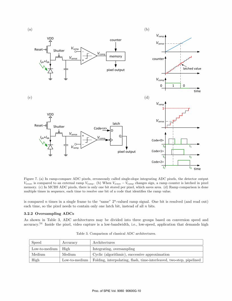
There has been much interest in adapting Nyquist-rate ADCs for pixel-level data conversion. The examplesillustrated here come from a research program at Stanford University that has resulted in commercialized DPStechnology. While the authors called one version of their design,31 illustrated in Figs. 7(a) and (b), a single-slopeintegrating ADC, it is technically a ramp-compare ADC, which has more in common with flash ADCs than withintegrating ADCs.
An n-bit flash ADC has 2n comparators that each perform one comparison in parallel. The ramp-compareADC replaces this parallel operation with a serial operation, where one comparator performs 2n comparisonsin sequence. A ramp voltage is generated and compared to the ADC input voltage. When there is a signchange in the comparison, a digital code representing the ramp voltage is latched. An n-bit digital-to-analogconverter (DAC) may be used to generate the ramp voltage in steps, as well as to provide the latched code, i.e.,the DAC input that triggers the sign change.
Yang et al.30 demonstrated a DPS array that is based on multichannel bit serial (MCBS) ADCs. The MCBSdesign, illustrated in Figs. 7(c) and (d), is similar to the ramp-compare design, but includes modifications thathave allowed it to be commercialized for visible-band applications. Unlike with the ramp-compare ADC, bitsare obtained in a serial manner to significantly reduce pixel area. For n-bit resolution, the “same” ADC input
Proc. of SPIE Vol. 9060 90600G-9
(a) (b)
counter
Vramp
pixel output
memoryVcomp
VDD
Reset
Iph+Idk
Vsense
Shutter -
+
Vramp
Vcomp
counter
0 01
Vsense
time
latched value
(c) (d)
D
pixel output
Vramp
+
-
VcompQ
latch
Code<n>
VDD
Reset
Iph+Idk
Vsense
Shutter
Code<0>
time
Code<1>
Code<2>
t0 t1
t1 t2
t2 t3
Vramp
1
Vsense
Figure 7. (a) In ramp-compare ADC pixels, erroneously called single-slope integrating ADC pixels, the detector outputVsense is compared to an external ramp Vramp. (b) When Vsense − Vramp changes sign, a ramp counter is latched in pixelmemory. (c) In MCBS ADC pixels, there is only one bit stored per pixel, which saves area. (d) Ramp comparison is donemultiple times in sequence, each time to resolve one bit of a code that identifies the ramp value.
is compared n times in a single frame to the “same” 2n-valued ramp signal. One bit is resolved (and read out)each time, so the pixel needs to contain only one latch bit, instead of all n bits.
3.2.2 Oversampling ADCs
As shown in Table 3, ADC architectures may be divided into three groups based on conversion speed andaccuracy.54 Inside the pixel, video capture is a low-bandwidth, i.e., low-speed, application that demands high
Table 3. Comparison of classical ADC architectures.
Speed Accuracy Architectures
Low-to-medium High Integrating, oversampling
Medium Medium Cyclic (algorithmic), successive approximation
High Low-to-medium Folding, interpolating, flash, time-interleaved, two-step, pipelined
Proc. of SPIE Vol. 9060 90600G-10

Iph+Idk
VDD VDD
Vb
+
1-bit DAC
−1-bit ADC∫ +
LPF and down-sampling
impulse response coefficients
select
sensor
1st order modulator decimator readout
high frequency digital signal
pixel output
Figure 8. A true ∆Σ ADC pixel, as shown, has both a modulator and decimator. The modulator oversamples and quantizesthe ADC input, while shaping noise to high frequencies. The decimator filters the modulator signal and down-samples itto the Nyquist rate. In this schematic, a logarithmic sensor is shown, but linear sensors may also be used.
bit-resolution, i.e., high accuracy, for high image quality. These specifications make oversampling ADCs, suchas delta-sigma (∆Σ) ADCs, especially suitable for pixel-level data conversion.
DPS arrays have been realized with first-order ∆Σ modulators inside each pixel.36–38 Higher-order ∆Σmodulators demonstrate better noise-shaping performance. However, they take more area and power. Although∆Σ modulators are oversampling ADCs, they are not ∆Σ ADCs. In a ∆Σ ADC, the digital output of themodulator is processed by a decimator, a digital circuit that performs low-pass filtering and down-sampling.Recently, Mahmoodi et al.39 presented a design, shown in Fig. 8, that includes in-pixel decimation.
Without in-pixel decimation, the bandwidth required to read the modulator outputs of a large array of pixelsmay be very high. As a result, either frame size, frame rate, or oversampling ratio has to be compromised.Lowering the oversampling ratio reduces the noise filtering and degrades the accuracy of the ∆Σ ADC. On theother hand, with in-pixel decimation, a large number of transistors are needed per pixel, which results in largerpixels. While this is acceptable for invisible-band applications, further efforts to shrink the in-pixel ∆Σ ADCare needed to apply the technology to visible-band applications competitively.
4. CONCLUSION
Transition to digital pixels can boost signal and noise figures of merit of CMOS image sensors. However, a largerpixel area makes DPS arrays less competitive for consumer electronics applications, which dominate the imagesensor market. Electronic imaging systems for medical, automotive, industrial, and security applications formlower-volume growing markets that can accept large pixels and benefit from DPS arrays. With many of thesesystems, imaging is done in invisible bands of the spectrum, such as X-ray and IR.
DPS arrays have been demonstrated with various architectures. Some used digitization techniques that areunique to imaging. Others adapted classical ADCs. Digital pixels not based on classical ADCs have beendemonstrated by exploiting PD and SPAD detectors. Classical Nyquist-rate ADCs have been used successfullyalso, some achieving small pixels. However, according to classical ADC theory, oversampling ADCs make thebest choice for low-speed high-accuracy applications, which are the specifications of DPS arrays.
ACKNOWLEDGMENTS
The authors thank Mr. Jing Li and Dr. Mark Alexiuk for technology and application advice. They are alsograteful to NSERC, TEC Edmonton, and IMRIS for financial and in-kind support.
Proc. of SPIE Vol. 9060 90600G-11

REFERENCES
1. W. Arden, M. Brillouet, P. Cogez, M. Graef, B. Huizing, and R. R. Mahnkopf, “More-than-Moore,” WhitePaper, International Technology Roadmap for Semiconductors, 2010.
2. ITRS, “2012 Update Overview,” Report, International Technology Roadmap for Semiconductors, 2012.
3. Frost & Sullivan, “Developments in Image Sensors,” Technical Insights, www.frost.com, 2012.
4. P. Danini and J. Baron, “Status of the CMOS Image Sensors Industry,” Presentation, Yole Developpment,2012.
5. K. P. Ziock, “Gamma-Ray Imaging Spectroscopy,” Science & Technology Review , pp. 14–26, Oct. 1995.
6. K. Spartiotis, A. Leppanen, T. Pantsar, J. Pyyhtia, P. Laukka, K. Muukkonen, O. Mannisto, J. Kinnari,and T. Schulman, “A photon counting CdTe gamma- and X-ray camera,” Nuclear Instruments and Methodsin Physics Research A 550, pp. 267–277, 2005.
7. P. Russo, A. S. Curion, G. Mettivier, L. Aloj, C. Caraco, and S. Lastoria, “The MediPROBE CdTe BasedCompact Gamma Camera,” in IFMBE Proceedings, pp. 556–558, 2009.
8. M. J. Yaffe and J. A. Rowlands, “X-ray Detectors for Digital Radiography,” Physics in Medicine andBiology 42(1), pp. 1–39, 1997.
9. S. Kasap, J. B. Frey, G. Belev, O. Tousignant, H. Mani, J. Greenspan, L. Laperriere, O. Bubon, A. Reznik,G. DeCrescenzo, K. S. Karim, and J. A. Rowlands, “Amorphous and polycrystalline photoconductors fordirect conversion flat panel x-ray image sensors,” Sensors 11(5), pp. 5112–5157, 2011.
10. ANRAD, “ANRAD Flat Panel Digital X-ray Detectors.” www.anrad.com, 2009.
11. Hamamatsu, “CCD area image sensors.” www.hamamatsu.com, 2011.
12. DALSA, “DALSA XiNEOS-1313 CMOS Flat-Panel Detector for High Frame Rate X-Ray Imaging.”www.teledynedalsa.com, 2010.
13. M. Lindner, S. Elstein, P. Lindner, J. M. Topaz, and A. J. Phillips, “Daylight corona discharge imager,” inEleventh International Symposium on High Voltage Engineering, 4, pp. 349–352, 1999.
14. Hamamatsu, “BT(Back-thinned)-CCD Cooled Digital Camera ORCA II-BT-512G.” www.hamamatsu.com,2006.
15. Intevac, “MicroVista-UV Back-Illuminated CMOS Camera.” www.intevac.com, 2012.
16. H. Eltoukhy, K. Salama, and A. El Gamal, “A 0.18-µm CMOS Bioluminescence Detection Lab-on-Chip,”IEEE Journal of Solid-State Circuits 41(3), pp. 651–662, 2006.
17. F. Niklaus, C. Vieider, and H. Jakobsen, “MEMS-Based Uncooled Infrared Bolometer Arrays: A Review,”in Proceedings of the SPIE, 6836, pp. 68360D 1–15, 2007.
18. Yole Developpment, “MicroTech is CleanTech,” in CMC Microsystems Annual Symposium, Oct. 2011.
19. F. Schuster, W. Knap, and V. Nguyen, “Terahertz imaging achieved with low-cost CMOS detectors,” LaserFocus World 47(7), pp. 37–41, 2011.
20. E. Ojefors, U. R. Pfeiffer, A. Lisauskas, and H. G. Roskos, “A 0.65 THz Focal-Plane Array in a Quarter-Micron CMOS Process Technology,” IEEE Journal of Solid-State Circuits 44(7), pp. 1968–1976, 2009.
21. S. Domingues, M. Perenzoni, D. Stoppa, A. D. Capobianco, and F. Sacchetto, “A CMOS THz staringimager with in-pixel electronics,” in 7th Conference on Ph.D. Research in Microelectronics and Electronics,pp. 81–84, July 2011.
22. M. Bolduc, M. Terroux, B. Tremblay, L. Marchese, E. Savard, M. Doucet, H. Oulachgar, C. Alain,H. Jerominek, and A. Bergeron, “Noise-equivalent power characterization of an uncooled microbolometer-based THz imaging camera,” in Proceedings of the SPIE, 8023, pp. 80230C 1–10, 2011.
23. Millennium Research Group, “US X-ray System Market to Reach Value of $2.8 Billion by 2016.”www.businesswire.com, 2012.
24. C. Li, G. D. Skidmore, and C. J. Han, “Uncooled Infrared Sensor Development Trends and Challenges,” inProceedings of the SPIE, 8155, pp. 815515 1–11, 2011.
25. X. Guo, X. Qi, and J. Harris, “A Time-to-First-Spike CMOS Image Sensor,” IEEE Sensors Journal 7(8),pp. 1165–1175, 2007.
26. A. Spivak, A. Belenky, A. Fish, and O. Yadid-Pecht, “Wide-Dynamic-Range CMOS Image Sensors—Comparative Performance Analysis,” IEEE Transactions on Electron Devices 56(11), pp. 2446–2461, 2009.
Proc. of SPIE Vol. 9060 90600G-12

27. X. Wang, W. Wong, and R. Hornsey, “A High Dynamic Range CMOS Image Sensor With Inpixel Light-to-Frequency Conversion,” IEEE Transactions on Electron Devices 53(12), pp. 2988–2992, 2006.
28. S. Cova, M. Ghioni, A. Lacaita, C. Samori, and F. Zappa, “Avalanche photodiodes and quenching circuitsfor single-photon detection,” Applied Optics 35(12), pp. 1956–1976, 1996.
29. A. Gallivanoni, I. Rech, and M. Ghioni, “Progress in quenching circuits for single photon avalanche diodes,”IEEE Transactions on Nuclear Science 57(6), pp. 3815–3826, 2010.
30. D. X. D. Yang, B. Fowler, and A. El Gamal, “A Nyquist-rate pixel-level ADC for CMOS image sensors,”IEEE Journal of Solid-State Circuits 34(3), pp. 348–356, 1999.
31. S. Kleinfelder, S. Lim, X. Liu, and A. El Gamal, “A 10000 frames/s CMOS digital pixel sensor,” IEEEJournal of Solid-State Circuits 36(12), pp. 2049–2059, 2001.
32. A. Kitchen, A. Bermak, and A. Bouzerdoum, “PWM digital pixel sensor based on asynchronous self-resettingscheme,” IEEE Electron Device Letters 25(7), pp. 471–473, 2004.
33. A. Bermak and Y.-F. Yung, “A DPS array with programmable resolution and reconfigurable conversiontime,” IEEE Transactions on Very Large Scale Integration Systems 14(1), pp. 15–22, 2006.
34. J. Crooks, S. Bohndiek, C. D. Arvanitis, R. Speller, H. XingLiang, E. Villani, M. Towrie, and R. Turchetta,“A CMOS Image Sensor With In-Pixel ADC, Timestamp, and Sparse Readout,” IEEE Sensors Journal 9(1),pp. 20–28, 2009.
35. K. Ito, B. Tongprasit, and T. Shibata, “A Computational Digital Pixel Sensor Featuring Block-ReadoutArchitecture for On-Chip Image Processing,” IEEE Transactions on Circuits and Systems I 56(1), pp. 114–123, 2009.
36. J. G. Rocha, G. Minas, and S. Lanceros-Mendez, “Pixel Readout Circuit for X-Ray Imagers,” IEEE SensorsJournal 10(11), pp. 1740–1745, 2010.
37. R. Figueras, J. Sabadell, L. Teres, and F. Serra-Graells, “A 70-µm Pitch 8-µW Self-Biased Charge-Integration Active Pixel for Digital Mammography,” IEEE Transactions on Biomedical Circuits and Sys-tems 5(5), pp. 481–489, 2011.
38. Z. Ignjatovic, D. Maricic, and M. Bocko, “Low Power, High Dynamic Range CMOS Image Sensor EmployingPixel-Level Oversampling Analog-to-Digital Conversion,” IEEE Sensors Journal 12(4), pp. 737–746, 2012.
39. A. Mahmoodi, J. Li, and D. Joseph, “Digital Pixel Sensor Array with Logarithmic Delta-Sigma Architec-ture,” Sensors 13(8), pp. 10765–10782, 2013.
40. X. Jin, Z. Liu, and J. Yang, “New Flash ADC Scheme With Maximal 13 Bit Variable Resolution andReduced Clipped Noise for High-Performance Imaging Sensor,” IEEE Sensors Journal 13(1), pp. 167–171,2013.
41. M. Loinaz, K. J. Singh, A. J. Blanksby, D. A. Inglis, K. Azadet, and B. D. Ackland, “A 200-mW, 3.3-V,CMOS color camera IC producing 352 × 288 24-b video at 30 frames/s,” IEEE Journal of Solid-StateCircuits 33(12), pp. 2092–2103, 1998.
42. J. Deguchi, F. Tachibana, M. Morimoto, M. Chiba, T. Miyaba, H. Tanaka, K. Takenaka, S. Funayama,K. Amano, K. Sugiura, R. Okamoto, and S. Kousai, “A 187.5µVrms-read-noise 51mW 1.4Mpixel CMOSimage sensor with PMOSCAP column CDS and 10b self-differential offset-cancelled pipeline SAR-ADC,”in IEEE International Solid-State Circuits Conference, pp. 494–495, 2013.
43. ON Semiconductor, “LUPA300 CMOS Image Sensor.” www.onsemi.com, 2013.
44. M.-H. Choi, G.-C. Ahn, and S.-H. Lee, “12b 50 MS/s 0.18 µm CMOS ADC with highly linear input variablegain amplifier,” Electronics Letters 46(18), pp. 1254–1256, 2010.
45. M.-W. Seo, T. Sawamoto, T. Akahori, Z. Liu, T. Iida, T. Takasawa, T. Kosugi, T. Watanabe, K. Isobe,and S. Kawahito, “A Low-Noise High-Dynamic-Range 17-b 1.3-Megapixel 30-fps CMOS Image SensorWith Column-Parallel Two-Stage Folding-Integration/Cyclic ADC,” IEEE Transactions on Electron De-vices 59(12), pp. 3396–3400, 2012.
46. K. Kitamura, T. Watabe, T. Sawamoto, T. Kosugi, T. Akahori, T. Iida, K. Isobe, T. Watanabe, H. Shi-mamoto, H. Ohtake, S. Aoyama, S. Kawahito, and N. Egami, “A 33-Megapixel 120-Frames-Per-Second 2.5-Watt CMOS Image Sensor With Column-Parallel Two-Stage Cyclic Analog-to-Digital Converters,” IEEETransactions on Electron Devices 59(12), pp. 3426–3433, 2012.
Proc. of SPIE Vol. 9060 90600G-13

47. M.-S. Shin, J.-B. Kim, M.-K. Kim, Y.-R. Jo, and O.-K. Kwon, “A 1.92-Megapixel CMOS Image Sensor WithColumn-Parallel Low-Power and Area-Efficient SA-ADCs,” IEEE Transactions on Electron Devices 59(6),pp. 1693–1700, 2012.
48. S. Matsuo, T. Bales, M. Shoda, S. Osawa, K. Kawamura, A. Andersson, M. Haque, H. Honda, B. Almond,Y. Mo, J. Gleason, T. Chow, and I. Takayanagi, “8.9-Megapixel Video Image Sensor With 14-b Column-Parallel SA-ADC,” IEEE Transactions on Electron Devices 56(11), pp. 2380–2389, 2009.
49. Y. Oike and A. El Gamal, “CMOS Image Sensor With Per-Column ∆Σ ADC and Programmable CompressedSensing,” IEEE Journal of Solid-State Circuits 48(1), pp. 318–328, 2013.
50. Y. Chae, J. Cheon, S. Lim, M. Kwon, K. Yoo, W. Jung, D.-H. Lee, S. Ham, and G. Han, “A 2.1 M Pixels, 120Frame/s CMOS Image Sensor With ∆Σ Column-Parallel ADC Architecture,” IEEE Journal of Solid-StateCircuits 46(1), pp. 236–247, 2011.
51. S.-F. Yeh and C.-C. Hsieh, “Novel Single-Slope ADC Design for Full Well Capacity Expansion of CMOSImage Sensor,” IEEE Sensors Journal 13(3), pp. 1012–1017, 2013.
52. D. Kim and M. Song, “An Enhanced Dynamic-Range CMOS Image Sensor Using a Digital LogarithmicSingle-Slope ADC,” IEEE Transactions on Circuits and Systems II 59(10), pp. 653–657, 2012.
53. BAE Systems, “CIS1021 Datasheet,” MAN 0103 Rev A, alliedscientificpro.com, 2011.
54. D. A. Johns and K. Martin, Analog Integrated Circuit Design, John Wiley & Sons, U.K., 1997.
Proc. of SPIE Vol. 9060 90600G-14