CMOS Active Pixel Sensor Technology for High …ericfossum.com/Publications/Papers/CMOS active pixel...
5
CMOS Active Pixel Sensor Technology for High Performance Machine Vision Applications Nicholas A. Doudoumopoulol Lauren Purcell 1 , and Eric R. Fossum 2 1 Photobit, LLC 2529 Foothill Blvd. Suite 104, La Crescenta, CA 91214 (818) 248-4393 fax (818) 542-3559 email: [email protected] 2 Jet Propulsion Laboratory,Califomia Institute of Technology 4800 Oak Grove Drive, Pasadena, CA 91109 Abstract A second generation image sensor technology has been developed at the NASA Jet Propulsion Laboratory as a result of the continuing need to miniaturize space science imaging instruments. Implemented using standard CMOS, the active pixel sensor (APS) technology permits the integration of the detector array with on-chip timing, control and signal chain electronics, including analog-to- digital conversion. The technology is now being commercialized and is well suited for high performance machine vision applications. Introduction Imaging system technology has broad applications in commercial, consumer, industrial, medical, defense and scientific markets. The development of the solid-state charge-coupled device (CCD) in the early 1970's led to relatively low cost, low power, and compact imaging systems compared to vidicons and other tube technology. The CCD uses repeated lateral transfer of charge in aMOS electrode-based analog shift register to enable readout of photogenerated signal electrons. High charge transfer efficiency (signal fidelity) is achieved using a highly specialized fabrication process that is not generally CMOS compatible. Separate support electronics are needed to provide timing, clocking and signal chain functions. CCDs, which are mostly capacitive devices, dissipate little power. On-chip dissipation arises mostly from the source-follower amplifier. The major power dissipation in a CCD system is in the support electronics. The CCD, as a chip-sized MOS capacitor, has a large C and requires large clock swings, 11Y, of the order of 5-15 Y to achieve high charge transfer 2 f efficiency. Thus, the CLly clock drive electronics dissipation is large. In addition, the need for various CCD clocking voltages (e.g. 7 or more different voltage levels) leads to numerous power supplies with attendant inefficiencies in conversion. Signal chain electronics that perform correlated double sampling (CDS) for noise reduction and amplification, and especially analog to digital converters (ADC), also dissipate significant power. CMOS Active Pixel Sensors Operation In an active pixel sensor, both the photodetector and readout amplifier are integrated within the pixel [1]. The voltage or current output from the cell is read out over X-Y wires instead of using a shift register. JPL has developed a CMOS active pixel sensor using standard CMOS technology that has achieved nearly the same performance as a CCD image sensor [2]. This is in contrast to previous CMOS image sensors or photodiode arrays that use a passive pixel architecture and achieve 10-1 OOx worse noise performance than a CCD. In addition, passive pixel sensors typically have slow readout times and are not well suited to large formats. The use of CMOS permits ready integration of on-chip timing and control electronics, as well as signal chain electronics. Analog to digital conversion can also be integrated on chip. Such a highly integrated imaging system is referred to as a camera-on-a-chip, and represents a second generation solid state image sensor technology. A block diagram of a CMOS active pixel circuit is shown below in Fig. 1. Incident photons pass through the photogate (PG) and generated electrons are integrated and stored under PG. For readout, a row is selected by enabling the row select transistor (RS). The floating diffusion output node (FD) is reset by pulsing transistor RST. The resultant voltage on FD is read out from the pixel onto the column bus using the in-pixel source follower. The voltage on the column bus is sampled onto a holding capacitor by pulsing transistor SHR. The signal charge is now transferred to FD by pulsing PG low. The voltage on FD drops in proportion to the number of SME Applied Machine Vision '96 - Emerging Smart Vision Sensors, Cincinnati, OH, June 1996. pg. I
Transcript of CMOS Active Pixel Sensor Technology for High …ericfossum.com/Publications/Papers/CMOS active pixel...
CMOS Active Pixel Sensor Technology for High Performance Machine Vision Applications
Nicholas A. Doudoumopoulol Lauren Purcell1, and Eric R. Fossum2
1Photobit, LLC 2529 Foothill Blvd. Suite 104, La Crescenta, CA 91214
(818) 248-4393 fax (818) 542-3559 email: [email protected]
2 Jet Propulsion Laboratory,Califomia Institute of Technology 4800 Oak Grove Drive, Pasadena, CA 91109
Abstract
A second generation image sensor technology has been developed at the NASA Jet Propulsion Laboratory as a result of the continuing need to miniaturize space science imaging instruments. Implemented using standard CMOS, the active pixel sensor (APS) technology permits the integration of the detector array with on-chip timing, control and signal chain electronics, including analog-todigital conversion. The technology is now being commercialized and is well suited for high performance machine vision applications.
Introduction
Imaging system technology has broad applications in commercial, consumer, industrial, medical, defense and scientific markets. The development of the solid-state charge-coupled device (CCD) in the early 1970's led to relatively low cost, low power, and compact imaging systems compared to vidicons and other tube technology. The CCD uses repeated lateral transfer of charge in aMOS electrode-based analog shift register to enable readout of photogenerated signal electrons. High charge transfer efficiency (signal fidelity) is achieved using a highly specialized fabrication process that is not generally CMOS compatible. Separate support electronics are needed to provide timing, clocking and signal chain functions. CCDs, which are mostly capacitive devices, dissipate little power. On-chip dissipation arises mostly from the source-follower amplifier. The major power dissipation in a CCD system is in the support electronics. The CCD, as a chip-sized MOS capacitor, has a large C and requires large clock swings, 11Y, of the order of 5-15 Y to achieve high charge transfer
2fefficiency. Thus, the CLly clock drive electronics dissipation is large. In addition, the need for various CCD clocking voltages (e.g. 7 or more different voltage levels) leads to numerous power supplies with attendant inefficiencies in conversion. Signal chain electronics that
perform correlated double sampling (CDS) for noise reduction and amplification, and especially analog to digital converters (ADC), also dissipate significant power.
CMOS Active Pixel Sensors
Operation In an active pixel sensor, both the photodetector and readout amplifier are integrated within the pixel [1]. The voltage or current output from the cell is read out over X-Y wires instead of using a shift register. JPL has developed a CMOS active pixel sensor using standard CMOS technology that has achieved nearly the same performance as a CCD image sensor [2]. This is in contrast to previous CMOS image sensors or photodiode arrays that use a passive pixel architecture and achieve 10-1 OOx worse noise performance than a CCD. In addition, passive pixel sensors typically have slow readout times and are not well suited to large formats.
The use of CMOS permits ready integration of on-chip timing and control electronics, as well as signal chain electronics. Analog to digital conversion can also be integrated on chip. Such a highly integrated imaging system is referred to as a camera-on-a-chip, and represents a second generation solid state image sensor technology.
A block diagram of a CMOS active pixel circuit is shown below in Fig. 1. Incident photons pass through the photogate (PG) and generated electrons are integrated and stored under PG. For readout, a row is selected by enabling the row select transistor (RS). The floating diffusion output node (FD) is reset by pulsing transistor RST. The resultant voltage on FD is read out from the pixel onto the column bus using the in-pixel source follower. The voltage on the column bus is sampled onto a holding capacitor by pulsing transistor SHR. The signal charge is now transferred to FD by pulsing PG low. The voltage on FD drops in proportion to the number of
SME Applied Machine Vision '96 - Emerging Smart Vision Sensors, Cincinnati, OH, June 1996. pg. I

photoelectrons and the capacitance of FD. The new voltage on the column bus is sampled onto a second capacitor by pulsing SHS. All pixels in a selected row are processed simultaneously and sampled onto capacitors at the bottom of their respective columns. The columnparallel sampling process typically takes 1-10 flsec, and occurs in the so-called horizontal blanking interval.
:--- ---- ---------voo----- ----:
PG TX
--L 1 RS1
.....• ~
FD
COL BUS:
PIXCKT
r - - - - - - - - - - - - - - - - - - - ~ - - - -
-------------COLCK,.-----------
Fig.i. CMOS APSpixel circuit (upper) and column circuit (lower)_ Load transistors not shown.
For readout, each column is successively selected by turning on column selection p-channel transistors CS. The p-channel source-followers in the column drive the signal (SIG) and horizontal reset (RST) bus lines. These lines are loaded by p-channel load transistors, not shown in Fig. I. The lines can either be sent directly to a pad for off-chip drive, or can be buffered.
Fig. 2. CMOS APS pixels.
Noise in the sensor is suppressed by the correlated double sampling (CDS) of the pixel output just after reset, before and after signal charge transfer to FD. The CDS suppresses kTC noise from pixel reset, suppresses 1/f noise from the in-pixel source follower, and suppresses fixed pattern noise (FPN) originating from pixel-to-pixel variation in source follower threshold voltage. kTC noise is reintroduced by sampling the signal onto the 1-4 pF capacitors at the bottom of the column. Typical output noise measured in CMOS APS arrays is of the order of 140-170 flY Lm.S. Output-referred conversion gain is typically 7-11 flV/e-, corresponding to noise of the order of 13-25 electrons Lm.S. This is similar to noise obtained in most commercial CCDs, though scientific CCDs have been reported with read noise in the 3-5 electrons Lm.S. The best CMOS APS performance to date has a noise level of 7 electrons Lm.S.
Power Typical biasing for each column's source-follower is 10 flA permitting charging of the sampling capacitors in the allotted time. The source-followers can then be turned off by cutting the voltage on each load transistor (not shown in Fig. 1.) The horizontal blanking interval is typically less than 10% of the line scan readout time, so that the sampling average power dissipation Ps corresponds to:
Ps = n I V d (1)
where n is number of columns, I is the load transistor bias, V is the supply voltage, and d is the duty cycle. Using n=5I2, I=lOflA, V=5V and d=IO%, a value for Ps of 2.5 mW is obtained.
To drive the horizontal bus lines at the video scan rate for analog output, a load current of I rnA or more is needed. The power dissipated is typically 5 mW.
Quantum Efficiency Quantum efficiency measured in CMOS APS arrays is similar to that for interline CCDs, and a typical curve is shown in Fig. 3. One interesting observation is that the quantum efficiency reflects significant responsivity in the "dead" part of the pixel containing the readout circuitry, as measured by intra pixel laser spot scanning [3]. This is because while the transistor gate and channel absorb photons with short absorption lengths (i.e. blue/green), longer wavelength photons penetrate through these regions and the subsequently generated carriers diffuse laterally to be collected by the photogate. Thus despite a fill factor of 25%-30%, the CMOS APS achieves quantum efficiencies
SME Applied Machine Vision '96 - Emerging Smart Vision Sensors, Cincinnati, OH, June 1996_ pg. 2

Fig. 4. Block diagram ofon-chip timing and control electronics.
The chip can be commanded to read out any area of interest within the array. The decoder counters can be preset to start and stop at any value that has been loaded into the chip via the 8-bit data bus. An alternate loading command is provided using the DEFAULT input line. Activation of this line forces all counters to a readout window of 128x128.
A programmable integration time is set by adjusting the delay between the end of one frame and the beginning of the next. This parameter is set by loading a 32-bit latch via the input data bus. A 32-bit counter operates from onefourth the clock input frequency and is preset each frame from the latch and so can provide very large integration delays. The input clock can be any frequency up to about
Fig. 6. Image ofa dollar bill taken with 256x256 sensor. 10 MHz. The pixel readout rate is tied to one-fourth the
that peak between 30%-35% in the red and near infrared. Microlenses can be added to improve quantum efficiency.
500 600 700 800 900 1000 1100
Wavelength (nm)
Fig. 3. Typical quantum efficiency ofa CMOS APS pixel.
On-Chip Timing and Control
Integration of on-chip timing and control circuits has been demonstrated in both 128x128 and 256x256 arrays [4]. A block diagram of the chip architecture is shown in Fig. 4. The analog outputs are VS_OUT (signal) and VR_OUT (reset), and the digital outputs are FRAME and READ. The inputs to the chip are asynchronous digital signals.
o " w
OJ<
"" DEFAULT LOAD
AOCRESS
""".5V
--e:>READ
--oFRAME
clock rate. Thus, frame rate is determined by the clock frequency, the window settings, and the delay integration time. A 30 Hz frame rate can be achieved without difficulty.
The column signal conditioning circuitry contains a double-delta sampling [4] FPN suppression stage that reduces FPN to below 0.2% sat with a random distribution. Power dissipation in the timing and control digital circuitry is minimal, and scales with clock rate. A photograph of a chip is shown in Fig. 5 and sample output in Fig. 6.
Fig. 5. Chip photograph of128x128 element CMOS APS with on-chip timing and control circuitry.
SME Applied Machine Vision '96 - Emerging Smart Vision Sensors, Cincinnati, OH, June /996. pg. 3
On-Chip Analog-to-Digital Converter (ADC)
On-chip ADC is desirable for several reasons. First, the chip becomes "digital" from a system designer's perspective, easing system design and packaging. Second, digital I/O improves immunity from system noise pickup. Third, component count is reduced. Fourth, while not immediately apparent, lower system power can be achieved, and possibly lower chip power dissipation as well [5].
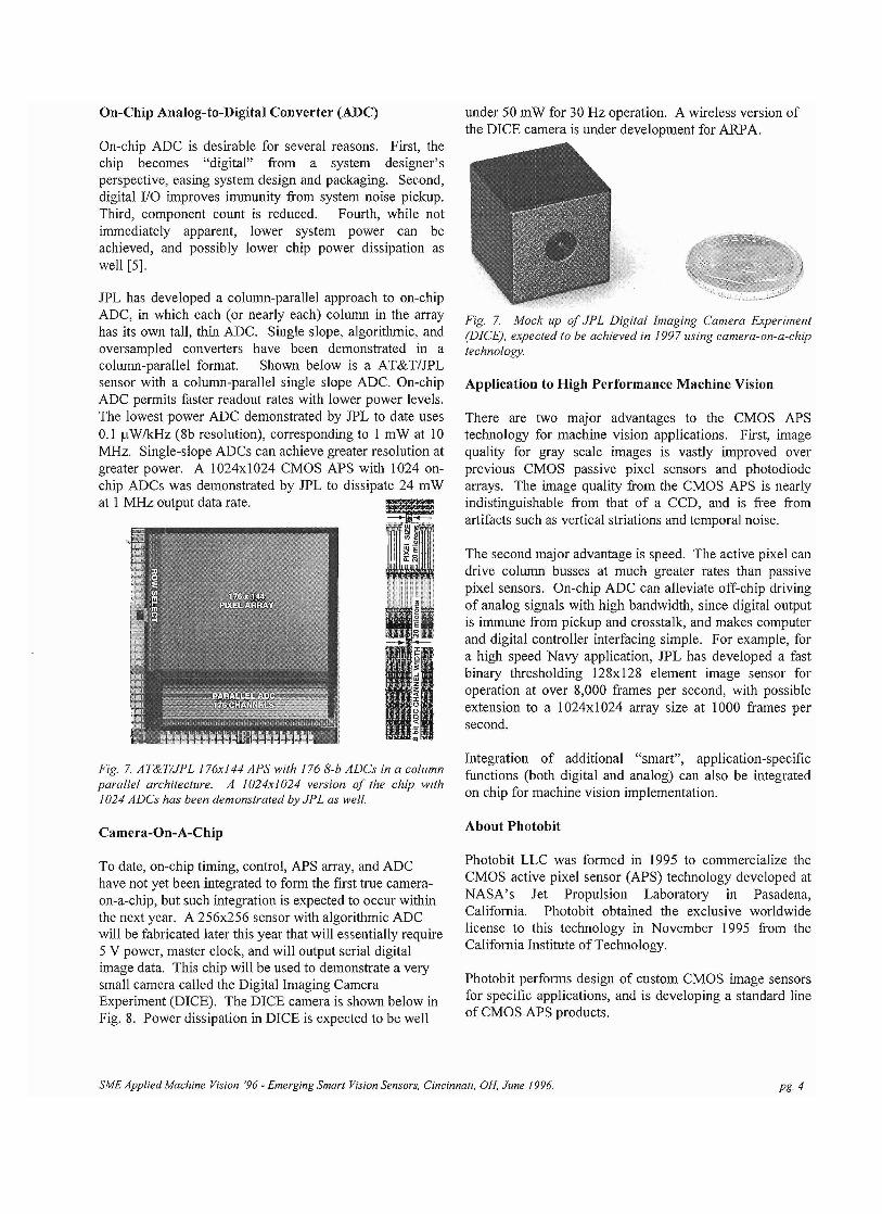
lPL has developed a column-parallel approach to on-chip ADC, in which each (or nearly each) column in the array has its own tall, thin ADC. Single slope, algorithmic, and oversampled converters have been demonstrated in a column-parallel format. Shown below is a AT&TIJPL sensor with a column-parallel single slope ADC. On-chip ADC permits faster readout rates with lower power levels. The lowest power ADC demonstrated by lPL to date uses 0.1 flW/kHz (8b resolution), corresponding to 1 mWat 10 MHz. Single-slope ADCs can achieve greater resolution at greater power. A 1024xl024 CMOS APS with 1024 onchip ADCs was demonstrated by JPL to dissipate 24 mW at 1 MHz output data rate.
Fig. 7. AT&TIJPL 176x144 APS with 176 8-b ADCs in a column parallel architecture. A 1024x1024 version of the chip with 1024 ADCs has been demonstrated byJPL as well.
Camera-On-A-Chip
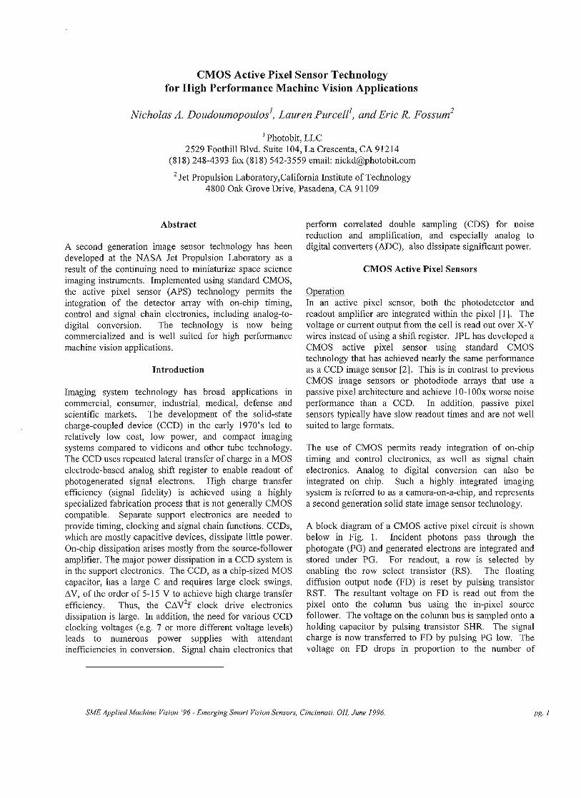
To date, on-chip timing, control, APS array, and ADC have not yet been integrated to form the first true cameraon-a-chip, but such integration is expected to occur within the next year. A 256x256 sensor with algorithmic ADC will be fabricated later this year that will essentially require 5 V power, master clock, and will output serial digital image data. This chip will be used to demonstrate a very small camera called the Digital Imaging Camera Experiment (DICE). The DICE camera is shown below in Fig. 8. Power dissipation in DICE is expected to be well
under 50 mW for 30 Hz operation. A wireless version of the DICE camera is under development for ARPA.
Fig. 7. Mock up of JPL Digital Imaging Camera Experiment (DICE), expected to be achieved in 1997 using camera-on-a-chip technology.
Application to High Performance Machine Vision
There are two major advantages to the CMOS APS technology for machine vision applications. First, image quality for gray scale images is vastly improved over previous CMOS passive pixel sensors and photodiode arrays. The image quality from the CMOS APS is nearly indistinguishable from that of a CCD, and is free from artifacts such as vertical striations and temporal noise.
The second major advantage is speed. The active pixel can drive column busses at much greater rates than passive pixel sensors. On-chip ADC can alleviate off-chip driving of analog signals with high bandwidth, since digital output is immune from pickup and crosstalk, and makes computer and digital controller interfacing simple. For example, for a high speed Navy application, lPL has developed a fast binary thresholding 128x128 element image sensor for operation at over 8,000 frames per second, with possible extension to a 1024x1024 array size at 1000 frames per second.
Integration of additional "smart", application-specific functions (both digital and analog) can also be integrated on chip for machine vision implementation.
About Photobit
Photobit LLC was formed in 1995 to commercialize the CMOS active pixel sensor (APS) technology developed at NASA's let Propulsion Laboratory in Pasadena, California. Photobit obtained the exclusive worldwide license to this technology in November 1995 from the California Institute of Technology.
Photobit performs design of custom CMOS image sensors for specific applications, and is developing a standard line of CMOS APS products.
SME Applied Machine Vision '96 - Emerging Smart Vision Sensors, Cincinnati, OH, June 1996. pg.4

Acknowledgments
The work reported in this paper represents the efforts of the lPL Advanced Imager Technology Group, Photobit LLC and associates, especially R. Nixon, S. Kemeny, B. Mansoorian, B.Pain, R. Panicacci, and C. Staller
I. E.R. Fossum, "Active pixel sensors -- are CCDs dinosaurs?", in CCDs and Optical Sensors 1II, Proc. SPIE vol. 1900, pp. 2-14, (!993).
2. S. Mendis, S.E. Kemeny, and E.R. Fossum, "CMOS active pixel image sensor," IEEE Trans. Electron Devices, vol. 41(3), pp.452-453 (1994).
3. S. Mendis, S.E. Kemeny, R. Gee, B. Pain, and E.R. Fossum, "Progress in CMOS active pixel image sensors," in CCDs and Optical Sensors IV, Proc. SPIE vol. 2172, pp. 19-29 (1994).
4. R.H. Nixon, S.E. Kemeny, e.O. Staller, and E.R. Fossum, "128x128 CMOS photodiode-type active pixel sensor with on-chip timing, control and signal chain electronics," in CCDs and Solid-Stale Optical Sensors V, Proc. SPIE vol. 2415, paper 34 (1995).
5. B. Pain and E.R. Fossum, "Approaches and analysis for on-focal-plane analog-to-digital conversion," in Infrared Readout Electronics 11, Proc. SPIE vol. 2226, pp. 208-218 (1994).
SME Applied Machine Vision '96 - Emerging Smart Vision Sensors, Cincinnati, OH, June 1996. pg. 5