
Intel® Cyclone® 10 LP Core Fabric and General Purpose I/Os ... · Intel Cyclone 10 LP Devices I/O...
174
Intel ® Cyclone ® 10 LP Core Fabric and General Purpose I/Os Handbook Subscribe Send Feedback C10LP51003 | 2019.01.24 Latest document on the web: PDF | HTML
Transcript of Intel® Cyclone® 10 LP Core Fabric and General Purpose I/Os ... · Intel Cyclone 10 LP Devices I/O...

Intel® Cyclone® 10 LP Core Fabricand General Purpose I/Os Handbook
SubscribeSend Feedback
C10LP51003 | 2019.01.24Latest document on the web: PDF | HTML

Contents
1. Logic Elements and Logic Array Blocks in Intel® Cyclone® 10 LP Devices....................... 61.1. Logic Elements......................................................................................................6
1.1.1. LE Features...............................................................................................71.1.2. LE Operating Modes................................................................................... 8
1.2. Logic Array Block................................................................................................. 101.2.1. LAB Interconnects....................................................................................111.2.2. LAB Control Signals..................................................................................12
1.3. Logic Elements and Logic Array Blocks in Intel Cyclone 10 LP Devices Revision History..14
2. Embedded Memory Blocks in Intel Cyclone 10 LP Devices.............................................152.1. Embedded Memory Capacity................................................................................. 152.2. Intel Cyclone 10 LP Embedded Memory General Features.......................................... 16
2.2.1. Control Signals........................................................................................ 162.2.2. Parity Bit................................................................................................ 172.2.3. Read Enable............................................................................................172.2.4. Byte Enable.............................................................................................172.2.5. Read-During-Write................................................................................... 192.2.6. Packed Mode Support............................................................................... 192.2.7. Address Clock Enable Support................................................................... 192.2.8. Asynchronous Clear..................................................................................20
2.3. Intel Cyclone 10 LP Embedded Memory Operation Modes.......................................... 212.3.1. Supported Memory Operation Modes.......................................................... 21
2.4. Intel Cyclone 10 LP Embedded Memory Clock Modes.................................................322.4.1. Asynchronous Clear in Clock Modes............................................................ 322.4.2. Output Read Data in Simultaneous Read and Write.......................................322.4.3. Independent Clock Enables in Clock Modes..................................................32
2.5. Intel Cyclone 10 LP Embedded Memory Configurations..............................................322.5.1. Port Width Configurations..........................................................................332.5.2. Memory Configurations for Dual-Port Modes................................................ 332.5.3. Maximum Block Depth Configuration.......................................................... 34
2.6. Intel Cyclone 10 LP Embedded Memory Design Consideration.................................... 342.6.1. Implement External Conflict Resolution....................................................... 342.6.2. Customize Read-During-Write Behavior.......................................................352.6.3. Consider Power-Up State and Memory Initialization...................................... 372.6.4. Control Clocking to Reduce Power Consumption........................................... 382.6.5. Selecting Read-During-Write Output Choices................................................38
2.7. Embedded Memory Blocks in Intel Cyclone 10 LP Devices Revision History...................38
3. Embedded Multipliers in Intel Cyclone 10 LP Devices....................................................393.1. Embedded Multiplier Block Overview.......................................................................393.2. Multipliers Resources in Intel Cyclone 10 LP Devices................................................. 413.3. Embedded Multipliers Architecture..........................................................................41
3.3.1. Input Register......................................................................................... 423.3.2. Multiplier Stage....................................................................................... 423.3.3. Output Register....................................................................................... 43
3.4. Embedded Multipliers Operational Modes.................................................................433.4.1. 18-Bit Multipliers..................................................................................... 443.4.2. 9-Bit Multipliers...................................................................................... 44
Contents
Intel® Cyclone® 10 LP Core Fabric and General Purpose I/Os Handbook Send Feedback
2

3.5. Embedded Multipliers in Intel Cyclone 10 LP Devices Revision History......................... 46
4. Clock Networks and PLLs in Intel Cyclone 10 LP Devices.............................................. 474.1. Clock Networks....................................................................................................47
4.1.1. GCLK Network......................................................................................... 474.1.2. GCLK Network Sources............................................................................. 474.1.3. Clock Control Block.................................................................................. 494.1.4. GCLK Network Clock Source Generation...................................................... 514.1.5. GCLK Network Power Down....................................................................... 524.1.6. Clock Enable Signals................................................................................ 53
4.2. PLLs in Intel Cyclone 10 LP Devices........................................................................ 544.2.1. PLL Features........................................................................................... 544.2.2. PLL Architecture.......................................................................................554.2.3. External Clock Outputs............................................................................. 564.2.4. Clock Feedback Modes..............................................................................574.2.5. Clock Multiplication and Division.................................................................594.2.6. Post-Scale Counter Cascading....................................................................604.2.7. Programmable Duty Cycle......................................................................... 614.2.8. PLL Control Signals.................................................................................. 614.2.9. Clock Switchover..................................................................................... 614.2.10. Programmable Bandwidth........................................................................664.2.11. Programmable Phase Shift.......................................................................664.2.12. PLL Cascading........................................................................................674.2.13. PLL Reconfiguration................................................................................ 674.2.14. Spread-Spectrum Clocking...................................................................... 74
4.3. Clock Networks and PLLs in Intel Cyclone 10 LP Devices Revision History.................... 75
5. I/O and High Speed I/O in Intel Cyclone 10 LP Devices............................................... 765.1. Intel Cyclone 10 LP I/O Standards Support..............................................................76
5.1.1. Intel Cyclone 10 LP I/O Standards Voltage and Pin Support........................... 785.2. I/O Resources in Intel Cyclone 10 LP Devices...........................................................80
5.2.1. Intel Cyclone 10 LP Devices I/O Resources Per Package................................805.2.2. Intel Cyclone 10 LP I/O Vertical Migration....................................................815.2.3. Intel Cyclone 10 LP VREF Pins Per I/O Bank.................................................815.2.4. Intel Cyclone 10 LP LVDS Channels Support ...............................................82
5.3. Intel FPGA I/O IP Cores for Intel Cyclone 10 LP Devices............................................ 845.4. Intel Cyclone 10 LP I/O Elements........................................................................... 85
5.4.1. Intel Cyclone 10 LP I/O Banks Architecture..................................................865.4.2. Intel Cyclone 10 LP I/O Banks Locations......................................................86
5.5. Intel Cyclone 10 LP Clock Pins Input Support...........................................................875.6. Programmable IOE Features in Intel Cyclone 10 LP Devices....................................... 88
5.6.1. Programmable Open Drain........................................................................ 885.6.2. Programmable Bus Hold............................................................................885.6.3. Programmable Pull-Up Resistor.................................................................. 895.6.4. Programmable Current Strength................................................................ 895.6.5. Programmable Output Slew Rate Control.....................................................905.6.6. Programmable IOE Delay.......................................................................... 915.6.7. PCI Clamp Diode......................................................................................925.6.8. Programmable Pre-Emphasis..................................................................... 93
5.7. I/O Standards Termination.................................................................................... 935.7.1. Voltage-Referenced I/O Standards Termination............................................ 94
Contents
Send Feedback Intel® Cyclone® 10 LP Core Fabric and General Purpose I/Os Handbook
3

5.7.2. Differential I/O Standards Termination........................................................ 955.7.3. Intel Cyclone 10 LP On-Chip I/O Termination............................................... 96
5.8. Intel Cyclone 10 LP High-Speed Differential I/Os and SERDES....................................995.8.1. High-Speed Differential I/O Interface........................................................ 1005.8.2. Differential I/O Standards Support............................................................1005.8.3. High-Speed I/O Timing Budget.................................................................107
5.9. Using the I/Os and High Speed I/Os in Intel Cyclone 10 LP Devices...........................1095.9.1. Guideline: Validate Your Pin Placement......................................................1095.9.2. Guideline: Check for Illegal Pad Placements............................................... 1095.9.3. Guideline: Voltage-Referenced I/O Standards Restriction............................. 1105.9.4. Guideline: Simultaneous Usage of Multiple I/O Standards ........................... 1105.9.5. Guideline: LVTTL or LVCMOS Inputs in Intel Cyclone 10 LP Devices............... 1115.9.6. Guideline: Differential Pad Placement........................................................1115.9.7. Guideline: Board Design for Signal Quality.................................................111
5.10. I/O and High Speed I/O in Intel Cyclone 10 LP Devices Revision History.................. 112
6. Configuration and Remote System Upgrades.............................................................. 1136.1. Configuration Schemes....................................................................................... 113
6.1.1. Active Serial (AS) Configuration............................................................... 1136.1.2. Passive Serial Configuration.....................................................................1196.1.3. Fast Passive Parallel Configuration............................................................ 1266.1.4. JTAG Configuration.................................................................................129
6.2. Configuration Requirement.................................................................................. 1416.2.1. Power-On Reset (POR) Circuit.................................................................. 1416.2.2. Configuration File Size............................................................................ 1426.2.3. Configuration and JTAG Pin I/O Requirements............................................ 142
6.3. Configuration Details.......................................................................................... 1436.3.1. MSEL Pin Settings.................................................................................. 1436.3.2. Configuration Sequence.......................................................................... 1456.3.3. Configuration Timing Waveforms.............................................................. 1486.3.4. Device Configuration Pins........................................................................ 150
6.4. Configuration Data Compression.......................................................................... 1516.4.1. Enabling Compression Before Design Compilation....................................... 1526.4.2. Enabling Compression After Design Compilation......................................... 1526.4.3. Using Compression in Multi-Device Configuration........................................153
6.5. Remote System Upgrades................................................................................... 1536.5.1. Enabling Remote Update......................................................................... 1546.5.2. Configuration Sequence in the Remote Update Mode...................................1556.5.3. Remote System Upgrade Circuitry............................................................ 1566.5.4. Remote System Upgrade Registers........................................................... 1566.5.5. Remote System Upgrade State Machine.................................................... 1596.5.6. User Watchdog Timer..............................................................................160
6.6. Configuration and Remote System Upgrades in Intel Cyclone 10 LP DevicesRevision History.............................................................................................. 161
7. SEU Mitigation in Intel Cyclone 10 LP Devices.............................................................1627.1. Configuration Error Detection...............................................................................1627.2. User Mode Error Detection...................................................................................1627.3. Error Detection Features..................................................................................... 163
7.3.1. Error Detection Block..............................................................................1637.4. Using Error Detection Features in User Mode..........................................................165
7.4.1. Enabling Error Detection......................................................................... 165
Contents
Intel® Cyclone® 10 LP Core Fabric and General Purpose I/Os Handbook Send Feedback
4
7.4.2. Accessing Error Detection Block Through User Logic....................................1667.5. SEU Mitigation for Intel Cyclone 10 LP Devices Revision History................................168
8. JTAG Boundary-Scan Testing for Intel Cyclone 10 LP Devices.....................................1698.1. BST Operation Control........................................................................................ 1698.2. I/O Voltage Support in the JTAG Chain.................................................................. 1708.3. Boundary-Scan Description Language Support....................................................... 1708.4. JTAG Boundary-Scan Testing for Intel Cyclone 10 LP Devices Revision History............ 171
9. Power Management in Intel Cyclone 10 LP Devices.................................................... 1729.1. External Power Supply Requirements.................................................................... 1729.2. Hot-Socketing Specifications................................................................................172
9.2.1. Drive Intel Cyclone 10 LP Devices Before Power Up.....................................1739.2.2. I/O Pins Remain Tri-stated During Power Up.............................................. 173
9.3. Hot-Socketing Feature Implementation................................................................. 1739.4. Power-On Reset Circuitry.................................................................................... 1739.5. Power Management in Intel Cyclone 10 LP Devices Revision History.......................... 174
Contents
Send Feedback Intel® Cyclone® 10 LP Core Fabric and General Purpose I/Os Handbook
5
1. Logic Elements and Logic Array Blocks in Intel®Cyclone® 10 LP Devices
The logic array block (LAB) is composed of logic elements (LEs). You can configure theLABs to implement logic functions, arithmetic functions, and register functions.
1.1. Logic Elements
LE is the smallest unit of logic in the Intel® Cyclone® 10 LP device family architecture.LEs are compact and provide advanced features with efficient logic usage.
Each LE has the following features:
• A four-input look-up table (LUT) that can implement any function of four variables
• A programmable register
• A carry chain connection
• A register chain connection
• The ability to drive the following interconnects:
— Local
— Row
— Column
— Register chain
— Direct link
• Register packing support
• Register feedback support
C10LP51003 | 2019.01.24
Send Feedback
Intel Corporation. All rights reserved. Intel, the Intel logo, Altera, Arria, Cyclone, Enpirion, MAX, Nios, Quartusand Stratix words and logos are trademarks of Intel Corporation or its subsidiaries in the U.S. and/or othercountries. Intel warrants performance of its FPGA and semiconductor products to current specifications inaccordance with Intel's standard warranty, but reserves the right to make changes to any products and servicesat any time without notice. Intel assumes no responsibility or liability arising out of the application or use of anyinformation, product, or service described herein except as expressly agreed to in writing by Intel. Intelcustomers are advised to obtain the latest version of device specifications before relying on any publishedinformation and before placing orders for products or services.*Other names and brands may be claimed as the property of others.
ISO9001:2015Registered

1.1.1. LE Features
LEs contain inputs, outputs, and registers to enable several features.
Figure 1. LE High-Level Block Diagram for Intel Cyclone 10 LP Devices.
Row, Column,And Direct Link Routing
data 1data 2data 3
data 4
labclr1labclr2
Chip-WideReset
(DEV_CLRn)
labclk1
labclk2
labclkena1
labclkena2
LE Carry-In
LAB-WideSynchronous
LoadLAB-Wide
Synchronous Clear
Row, Column,And Direct Link Routing
Local Routing
Register ChainOutput
Register Bypass
ProgrammableRegister
Register ChainRouting from
previous LE
LE Carry-Out
Register Feedback
SynchronousLoad and
Clear Logic
CarryChain
Look-Up Table(LUT)
Asynchronous Clear Logic
Clock &Clock Enable
Select
D Q
ENACLRN
LE Inputs
Each LE input is directed to different destinations to implement the desired logicfunction. In both the normal or arithmetic operating modes of the LE, there are sixavailable inputs:
• Four data inputs from the LAB local interconnect
• One LE carry-in from the previous LE carry-chain
• One register chain connection
LE Outputs
Each LE has three general routing outputs:
• Two LE outputs drive the column or row and direct link routing connections
• One LE output drives the local interconnect resources
Intel Cyclone 10 LP devices support register packing. With register packing, the LUT orregister output drives the three outputs independently. This feature improves deviceutilization by using the register and the LUT for unrelated functions.
The LAB-wide synchronous load control signal is not available if you use registerpacking.
1. Logic Elements and Logic Array Blocks in Intel® Cyclone® 10 LP Devices
C10LP51003 | 2019.01.24
Send Feedback Intel® Cyclone® 10 LP Core Fabric and General Purpose I/Os Handbook
7

Register Chain Output
Each LE has a register chain output that allows registers in the same LAB to cascadetogether. This feature speeds up connections between LABs and optimizes localinterconnect resources:
• LUTs are used for combinational functions
• Registers are used for an unrelated shift register implementation
Programmable Register
You can configure the programmable register of each LE for D, T, JK, or SR flipflopoperation. Each register has the following inputs:
• Clock—driven by signals that use the global clock network, general-purpose I/Opins, or internal logic
• Clear—driven by signals that use the global clock network, general-purpose I/Opins, or internal logic
• Clock enable—driven by the general-purpose I/O pins or internal logic
For combinational functions, the LUT output bypasses the register and drives directlyto the LE outputs.
Register Feedback
The register feedback mode allows the register output to feed back into the LUT of thesame LE. Register feedback ensures that the register is packed with its own fan-outLUT, providing another mechanism for improving fitting. The LE can also drive outregistered and unregistered versions of the LUT output.
1.1.2. LE Operating Modes
The LEs in Intel Cyclone 10 LP devices operate in two modes.
• Normal mode
• Arithmetic mode
These operating modes use LE resources differently. Both LE modes have six availableinputs and LAB-wide signals.
The Intel Quartus® Prime software automatically chooses the appropriate mode forcommon functions, such as counters, adders, subtractors, and arithmetic functions, inconjunction with parameterized functions such as the library of parameterizedmodules (LPM) functions.
You can also create special-purpose functions that specify which LE operating mode touse for optimal performance.
1.1.2.1. Normal Mode
Normal mode is suitable for general logic applications and combinational functions.
In normal mode, four data inputs from the LAB local interconnect are inputs to a four-input LUT. The Intel Quartus Prime Compiler automatically selects the carry-in (cin) orthe data3 signal as one of the inputs to the LUT. LEs in normal mode support packedregisters and register feedback.
1. Logic Elements and Logic Array Blocks in Intel® Cyclone® 10 LP Devices
C10LP51003 | 2019.01.24
Intel® Cyclone® 10 LP Core Fabric and General Purpose I/Os Handbook Send Feedback
8

Figure 2. LE Operating in Normal Mode for Intel Cyclone 10 LP devices
data1
Four-InputLUT
data2data3cin (from cout of previous LE)
data4clock (LAB Wide)
ena (LAB Wide)aclr (LAB Wide)
CLRN
DQ
ENA
sclear(LAB Wide)
sload(LAB Wide)
Register ChainConnection
RegisterChain Output
Row, Column, andDirect Link Routing
Row, Column, andDirect Link Routing
Local Routing
Register Bypass
Packed Register Input
Register Feedback
1.1.2.2. Arithmetic Mode
Arithmetic mode is ideal for implementing adders, counters, accumulators, andcomparators.
The LE in arithmetic mode implements a two-bit full adder and basic carry chain. LEsin arithmetic mode can drive out registered and unregistered versions of the LUToutput. Register feedback and register packing are supported when LEs are used inarithmetic mode.
Figure 3. LE Operating in Arithmetic Mode for Intel Cyclone 10 LP devices
clock (LAB Wide)ena (LAB Wide)aclr (LAB Wide)
CLRN
DQ
ENA
sclear(LAB Wide)
sload(LAB Wide)
RegisterChain Output
Row, Column, andDirect link routing
Row, Column, andDirect link routing
Local Routing
Register Feedback
Three-InputLUT
Three-InputLUTcin (from cout
of previous LE)
data2data1
cout
Register Bypass
data4
data3
Register ChainConnection
Packed Register Input
1. Logic Elements and Logic Array Blocks in Intel® Cyclone® 10 LP Devices
C10LP51003 | 2019.01.24
Send Feedback Intel® Cyclone® 10 LP Core Fabric and General Purpose I/Os Handbook
9

Carry Chain
The Intel Quartus Prime Compiler automatically creates carry chain logic during designprocessing. You can also manually create the carry chain logic during design entry.Parameterized functions, such as LPM functions, automatically take advantage of carrychains for the appropriate functions. The Intel Quartus Prime Compiler creates carrychains longer than 16 LEs by automatically linking LABs in the same column.
To enhanced fitting, a long carry chain runs vertically, which allows fast horizontalconnections to M9K memory blocks or embedded multipliers through direct linkinterconnects. For example, if a design has a long carry chain in an LAB column nextto a column of M9K memory blocks, any LE output can feed an adjacent M9K memoryblock through the direct link interconnect.
If the carry chains run horizontally, any LAB which is not next to the column of M9Kmemory blocks uses other row or column interconnects to drive a M9K memory block.
A carry chain continues as far as a full column.
1.2. Logic Array Block
The LABs are configurable logic blocks that consist of a group of logic resources.
Each LAB consists of the following:
• 16 logic elements (LEs)—smallest logic unit in Intel Cyclone 10 LP devices
• LE carry chains—carry chains propagated serially through each LE within an LAB
• LAB control signals—dedicated logic for driving control signals to LEs within an LAB
• Local interconnect—transfers signals between LEs in the same LAB
• Register chains—transfers the output of one LE register to the adjacent LE registerin an LAB
1. Logic Elements and Logic Array Blocks in Intel® Cyclone® 10 LP Devices
C10LP51003 | 2019.01.24
Intel® Cyclone® 10 LP Core Fabric and General Purpose I/Os Handbook Send Feedback
10

Figure 4. LAB Structure of Intel Cyclone 10 LP Devices
Direct linkinterconnectfrom adjacentblock
Direct linkinterconnectto adjacentblock
Row Interconnect
Column Interconnect
Local InterconnectLAB
Direct linkinterconnectfrom adjacentblock
Direct linkinterconnectto adjacentblock
The Intel Quartus Prime Compiler places associated logic in an LAB or adjacent LABs,allowing the use of local and register chain connections for performance and areaefficiency.
1.2.1. LAB Interconnects
The LAB local interconnect is driven by column and row interconnects and LE outputsin the same LAB.
The direct link connection minimizes the use of row and column interconnects toprovide higher performance and flexibility. The direct link connection enables theneighboring elements from left and right to drive the local interconnect of an LAB. Theelements are:
• LABs
• PLLs
• M9K embedded memory blocks
• Embedded multipliers
Each LE can drive up to 48 LEs through local and direct link interconnects.
1. Logic Elements and Logic Array Blocks in Intel® Cyclone® 10 LP Devices
C10LP51003 | 2019.01.24
Send Feedback Intel® Cyclone® 10 LP Core Fabric and General Purpose I/Os Handbook
11

Figure 5. LAB Local and Direct Link Interconnects for Intel Cyclone 10 LP Devices
LAB
Direct linkinterconnectto right
Direct link interconnect fromright LAB, M9K memoryblock, embedded multiplier,PLL, or IOE output
Direct link interconnect fromleft LAB, M9K memory
block, embedded multiplier,PLL, or IOE output
LocalInterconnect
Direct linkinterconnect
to left
LEs
1.2.2. LAB Control Signals
Each LAB contains dedicated logic for driving control signals to its LEs.
The control signals include:
• Two clock signals
• Two clock enable signals
• Two asynchronous clear signals
• One synchronous clear signal
• One synchronous load signal
1. Logic Elements and Logic Array Blocks in Intel® Cyclone® 10 LP Devices
C10LP51003 | 2019.01.24
Intel® Cyclone® 10 LP Core Fabric and General Purpose I/Os Handbook Send Feedback
12

Figure 6. LAB-Wide Control Signals for Intel Cyclone 10 LP Devices
labclkena1
labclk2labclk1
labclkena2 labclr1
DedicatedLAB RowClocks
LocalInterconnect
LocalInterconnect
LocalInterconnect
LocalInterconnect
syncload
synclr
labclr2
6
Table 1. Control Signal Descriptions for Intel Cyclone 10 LP Devices
Control Signal Description
labclk1 • Each LAB can use two clocks signals. The clock and clock enable signals of each LAB arelinked. For example, any LE in a particular LAB using the labclk1 signal also uses thelabclkena1 signal.
• If the LAB uses both the rising and falling edges of a clock, it also uses both LAB-wide clocksignals.
• The LAB row clocks [5..0] and LAB local interconnect generate the LAB-wide clock signals.The MultiTrack interconnect inherent low skew allows clock and control signal distribution inaddition to data distribution.
labclk2
labclkena1 • Each LAB can use two clock enable signals. The clock and clock enable signals of each LABare linked. For example, any LE in a particular LAB using the labclk1 signal also uses thelabclkena1 signal.
• Deasserting the clock enable signal turns off the LAB-wide clock signal.labclkena2
labclr1 Asynchronous clear signals:• LAB-wide control signals that control the logic for the clear signal of the register.• The LE directly supports an asynchronous clear function.labclr2
syncload Synchronous load and synchronous clear signals:• Can be used for implementing counters and other functions• LAB-wide control signals that affect all registers in the LABsynclr
You can use up to eight control signals at a time. Register packing and synchronousload cannot be used simultaneously.
Each LAB can have up to four non-global control signals. You can use additional LABcontrol signals as long as they are global signals.
An LAB-wide asynchronous load signal to control the logic for the preset signal of theregister is not available. The register preset is achieved with a NOT gate push-backtechnique. Intel Cyclone 10 LP devices only support either a preset or asynchronousclear signal.
In addition to the clear port, Intel Cyclone 10 LP devices provide a chip-wide reset pin(DEV_CLRn) to reset all registers in the device. An option set before compilation in theIntel Quartus Prime software controls this pin. This chip-wide reset overrides all othercontrol signals.
1. Logic Elements and Logic Array Blocks in Intel® Cyclone® 10 LP Devices
C10LP51003 | 2019.01.24
Send Feedback Intel® Cyclone® 10 LP Core Fabric and General Purpose I/Os Handbook
13
1.3. Logic Elements and Logic Array Blocks in Intel Cyclone 10 LPDevices Revision History
Date Version Changes
May 2017 2017.05.08 Initial release.
1. Logic Elements and Logic Array Blocks in Intel® Cyclone® 10 LP Devices
C10LP51003 | 2019.01.24
Intel® Cyclone® 10 LP Core Fabric and General Purpose I/Os Handbook Send Feedback
14

2. Embedded Memory Blocks in Intel Cyclone 10 LPDevices
The Intel Cyclone 10 LP embedded memory structure consists of columns of M9Kmemory block. You can configure each M9K block in different widths andconfigurations to provide various memory functions such as RAM, ROM, shift registers,and FIFO buffers.
Related Information
• Embedded Memory (RAM: 1-PORT, RAM: 2-PORT, ROM: 1-PORT, and ROM: 2-PORT) User Guide
Provides more information about the supported modes, signals, andparameters of the embedded memory IP cores that support the M9K blocks inthe Intel Cyclone 10 LP devices.
• Introduction to Intel FPGA IP CoresProvides general information about all Intel FPGA IP cores, includingparameterizing, generating, upgrading, and simulating IP cores.
• Creating Version-Independent IP and Qsys Simulation ScriptsCreate simulation scripts that do not require manual updates for software or IPversion upgrades.
• Project Management Best PracticesGuidelines for efficient management and portability of your project and IP files.
2.1. Embedded Memory Capacity
Table 2. Embedded Memory Capacity in Intel Cyclone 10 LP Devices
Device M9K Blocks RAM Capacity (Kb)
10CL006 30 270
10CL010 46 414
10CL016 56 504
10CL025 66 594
10CL040 126 1,134
10CL055 260 2,340
10CL080 305 2,745
10CL120 432 3,888
C10LP51003 | 2019.01.24
Send Feedback
Intel Corporation. All rights reserved. Intel, the Intel logo, Altera, Arria, Cyclone, Enpirion, MAX, Nios, Quartusand Stratix words and logos are trademarks of Intel Corporation or its subsidiaries in the U.S. and/or othercountries. Intel warrants performance of its FPGA and semiconductor products to current specifications inaccordance with Intel's standard warranty, but reserves the right to make changes to any products and servicesat any time without notice. Intel assumes no responsibility or liability arising out of the application or use of anyinformation, product, or service described herein except as expressly agreed to in writing by Intel. Intelcustomers are advised to obtain the latest version of device specifications before relying on any publishedinformation and before placing orders for products or services.*Other names and brands may be claimed as the property of others.
ISO9001:2015Registered

2.2. Intel Cyclone 10 LP Embedded Memory General Features
Intel Cyclone 10 LP embedded memory supports the following general features:
• 8,192 memory bits per block (9,216 bits per block including parity).
• Independent read-enable (rden) and write-enable (wren) signals for each port.
• Packed mode in which the M9K memory block is split into two 4.5 K single-portRAMs.
• Variable port configurations.
• Single-port and simple dual-port modes support for all port widths.
• True dual-port (one read and one write, two reads, or two writes) operation.
• Byte enables for data input masking during writes.
• Two clock-enable control signals for each port (port A and port B).
• Initialization file to preload memory content in RAM and ROM modes.
2.2.1. Control Signals
The clock-enable control signal controls the clock entering the input and outputregisters and the entire M9K memory block. This signal disables the clock so that theM9K memory block does not see any clock edges and does not perform anyoperations.
The rden and wren control signals control the read and write operations for each portof the M9K memory blocks. You can disable the rden or wren signals independentlyto save power whenever the operation is not required.
Figure 7. Register Clock, Clear, and Control Signals Implementation in M9K EmbeddedMemory Block
clock_b
clocken_aclock_a
clocken_b aclr_b
aclr_a
DedicatedRow LABClocks
rden_b
rden_a
6
LocalInterconnect
byteena_b
byteena_a
addressstall_b
addressstall_awren_a
wren_b
2. Embedded Memory Blocks in Intel Cyclone 10 LP Devices
C10LP51003 | 2019.01.24
Intel® Cyclone® 10 LP Core Fabric and General Purpose I/Os Handbook Send Feedback
16
2.2.2. Parity Bit
You can perform parity checking for error detection with the parity bit along withinternal logic resources. The M9K memory blocks support a parity bit for each storagebyte. You can use this bit as either a parity bit or as an additional data bit. No parityfunction is actually performed on this bit. If error detection is not desired, you can usethe parity bit as an additional data bit.
2.2.3. Read Enable
M9K memory blocks support the read enable feature for all memory modes.
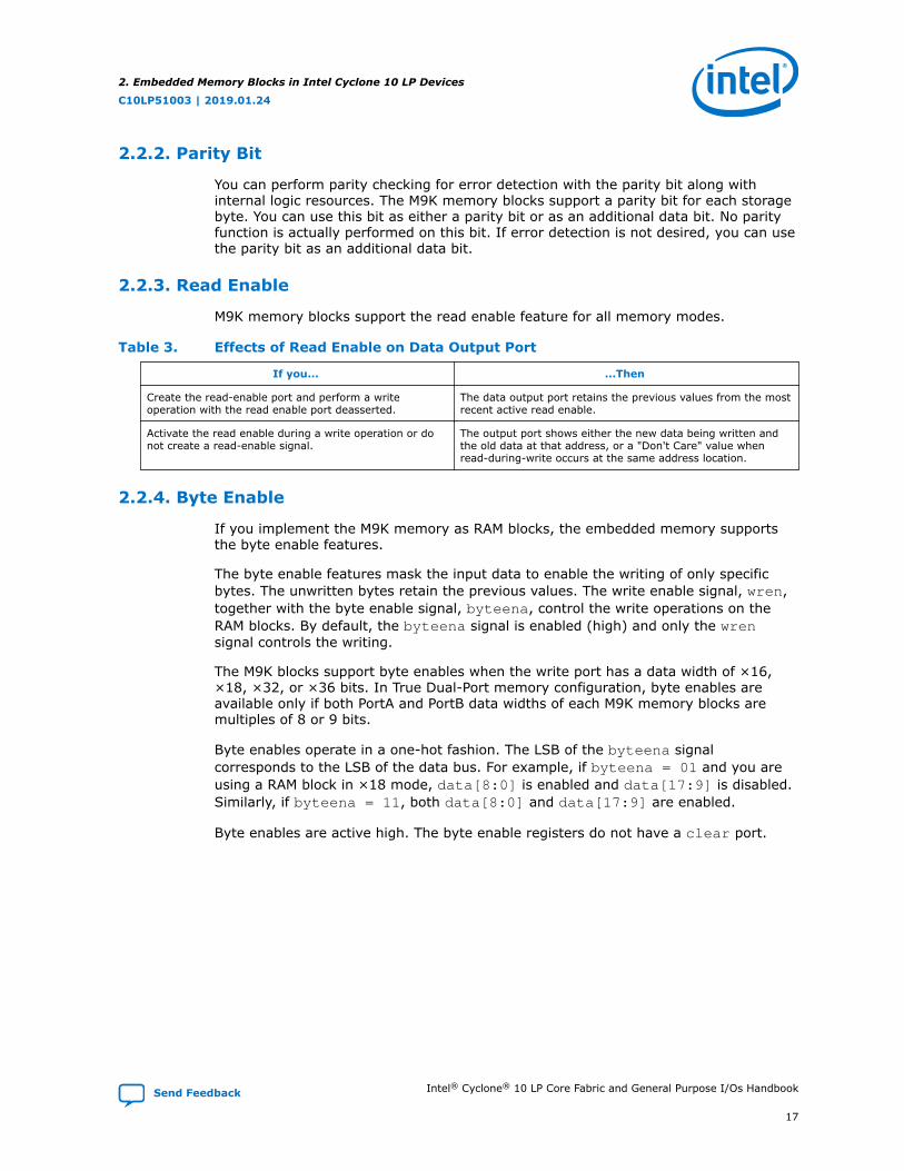
Table 3. Effects of Read Enable on Data Output Port
If you... ...Then
Create the read-enable port and perform a writeoperation with the read enable port deasserted.
The data output port retains the previous values from the mostrecent active read enable.
Activate the read enable during a write operation or donot create a read-enable signal.
The output port shows either the new data being written andthe old data at that address, or a "Don't Care" value whenread-during-write occurs at the same address location.
2.2.4. Byte Enable
If you implement the M9K memory as RAM blocks, the embedded memory supportsthe byte enable features.
The byte enable features mask the input data to enable the writing of only specificbytes. The unwritten bytes retain the previous values. The write enable signal, wren,together with the byte enable signal, byteena, control the write operations on theRAM blocks. By default, the byteena signal is enabled (high) and only the wrensignal controls the writing.
The M9K blocks support byte enables when the write port has a data width of ×16,×18, ×32, or ×36 bits. In True Dual-Port memory configuration, byte enables areavailable only if both PortA and PortB data widths of each M9K memory blocks aremultiples of 8 or 9 bits.
Byte enables operate in a one-hot fashion. The LSB of the byteena signalcorresponds to the LSB of the data bus. For example, if byteena = 01 and you areusing a RAM block in ×18 mode, data[8:0] is enabled and data[17:9] is disabled.Similarly, if byteena = 11, both data[8:0] and data[17:9] are enabled.
Byte enables are active high. The byte enable registers do not have a clear port.
2. Embedded Memory Blocks in Intel Cyclone 10 LP Devices
C10LP51003 | 2019.01.24
Send Feedback Intel® Cyclone® 10 LP Core Fabric and General Purpose I/Os Handbook
17

2.2.4.1. Byte Enable Controls
Table 4. M9K Blocks Byte Enable Selections
byteena[3:0]Affected Bytes. Any Combination of Byte Enables is Possible.
datain x 16 datain x 18 datain x 32 datain x 36
[0] = 1 [7:0] [8:0] [7:0] [8:0]
[1] = 1 [15:8] [17:9] [15:8] [17:9]
[2] = 1 — — [23:16] [26:18]
[3] = 1 — — [31:24] [35:27]
2.2.4.2. Data Byte Output
If you... ...Then
Deassert a byte-enable bit during a write cycle The old data in the memory appears in the correspondingdata-byte output.
Assert a byte-enable bit during a write cycle The corresponding data-byte output depends on the IntelQuartus Prime software setting. The setting can be eitherthe newly written data or the old data at that location.
2.2.4.3. RAM Blocks Operations
Figure 8. Byte Enable Functional WaveformThis figure shows how the wren and byteena signals control the RAM operations.
inclock
wren
address
data
q (asynch)
an
XXXX
a0 a1 a2 a0 a1 a2
doutn ABFF FFCD ABCD ABFF FFCD
ABCD
byteena XX 10 01 11
XXXX
XX
ABCD
ABCDFFFF
FFFF
FFFF
ABFF
FFCD
contents at a0
contents at a1
contents at a2
rden
For this functional waveform, New Data Mode is selected.
2. Embedded Memory Blocks in Intel Cyclone 10 LP Devices
C10LP51003 | 2019.01.24
Intel® Cyclone® 10 LP Core Fabric and General Purpose I/Os Handbook Send Feedback
18

2.2.5. Read-During-Write
The read-during-write operation occurs when a read operation and a write operationtarget the same memory location at the same time.
The read-during-write operation operates in the following ways:
• Same-port
• Mixed-port
2.2.6. Packed Mode Support
You can implement two single-port memory blocks in a single block under thefollowing conditions:
• Each of the two independent block sizes is less than or equal to half of the M9Kblock size. The maximum data width for each independent block is 18 bits wide.
• Each of the single-port memory blocks is configured in single-clock mode.
Related Information
• Supported Memory Operation Modes on page 21Provides more information about the single-port mode.
• Intel Cyclone 10 LP Embedded Memory Clock Modes on page 32Provides more information about the single-clock mode.
2.2.7. Address Clock Enable Support
You can use the address clock enable feature to improve the effectiveness of cachememory applications during a cache-miss. If you configure M9K memory blocks indual-port mode, each port has its own independent address clock enable.
By default, the address clock enable signal, addressstall, is disabled and the signalis active low. While the addressstall signal is high (addressstall = 1), theaddress register holds the previous address value.
Figure 9. Address Clock Enable Block DiagramIn this diagram, the address register output feeds back to its input using a multiplexer. The addressstallsignal selects the multiplexer output.
address[0]
address[N]addressstall
clock
address[0]register
address[N]register
address[N]
address[0]
2. Embedded Memory Blocks in Intel Cyclone 10 LP Devices
C10LP51003 | 2019.01.24
Send Feedback Intel® Cyclone® 10 LP Core Fabric and General Purpose I/Os Handbook
19
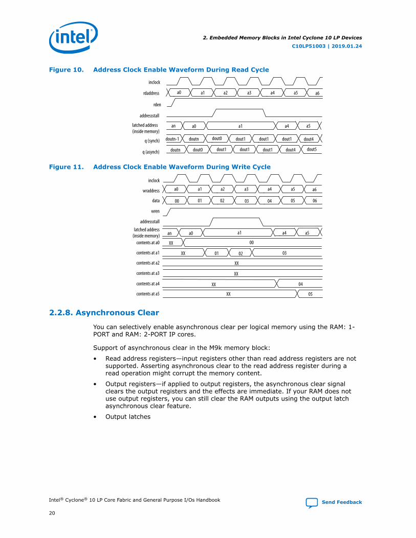
Figure 10. Address Clock Enable Waveform During Read Cycle
inclock
rden
rdaddress
q (synch)
a0 a1 a2 a3 a4 a5 a6
q (asynch)
an a0 a4 a5latched address(inside memory)
dout0 dout1 dout1 dout4
dout1 dout4 dout5
addressstall
a1
doutn-1 dout1doutn
doutn dout1dout0 dout1
Figure 11. Address Clock Enable Waveform During Write Cycle
inclock
wren
wraddress a0 a1 a2 a3 a4 a5 a6
an a0 a4 a5latched address
(inside memory)
addressstall
a1
data 00 01 02 03 04 05 06
contents at a0
contents at a1
contents at a2
contents at a3
contents at a4
contents at a5
XX
04XX
00
0301XX 02
XX
XX
XX 05
2.2.8. Asynchronous Clear
You can selectively enable asynchronous clear per logical memory using the RAM: 1-PORT and RAM: 2-PORT IP cores.
Support of asynchronous clear in the M9k memory block:
• Read address registers—input registers other than read address registers are notsupported. Asserting asynchronous clear to the read address register during aread operation might corrupt the memory content.
• Output registers—if applied to output registers, the asynchronous clear signalclears the output registers and the effects are immediate. If your RAM does notuse output registers, you can still clear the RAM outputs using the output latchasynchronous clear feature.
• Output latches
2. Embedded Memory Blocks in Intel Cyclone 10 LP Devices
C10LP51003 | 2019.01.24
Intel® Cyclone® 10 LP Core Fabric and General Purpose I/Os Handbook Send Feedback
20

Figure 12. Output Latch Asynchronous Clear Waveform
aclr
aclr at latch
clk
q a1 a0 a1a2
Related Information
Asynchronous Clear, Embedded Memory (RAM: 1-PORT, RAM: 2-PORT, ROM: 1-PORT,and ROM: 2-PORT) User Guide
Provides more information about asynchronous clears in the embedded memory IPcore.
2.2.8.1. Resetting Registers in M9K Blocks
There are three ways to reset registers in the M9K blocks:
• Power up the device
• Use the aclr signal for output register only
• Assert the device-wide reset signal using the DEV_CLRn option
2.3. Intel Cyclone 10 LP Embedded Memory Operation Modes
The M9K memory blocks allow you to implement fully-synchronous SRAM memory inmultiple operation modes. The M9K memory blocks do not support asynchronous(unregistered) memory inputs.
Note: Violating the setup or hold time on the M9K memory block input registers may corruptmemory contents. This applies to both read and write operations.
2.3.1. Supported Memory Operation Modes
Table 5. Supported Memory Operation Modes in the M9K Embedded Memory Blocks
Memory OperationMode
Related IP Core Description
Single-port RAM RAM: 1-PORT IP Core Single-port mode supports non-simultaneous read and writeoperations from a single address.Use the read enable port to control the RAM output ports behaviorduring a write operation:• To show either the new data being written or the old data at
that address, activate the read enable (rden) during a writeoperation.
• To retain the previous values that are held during the mostrecent active read enable, perform the write operation with theread enable port deasserted.
Simple dual-port RAM RAM: 2-PORT IP Core You can simultaneously perform one read and one write operationsto different locations where the write operation happens on Port Aand the read operation happens on Port B.In this memory mode, the M9K memory blocks support separatewren and rden signals. To save power, keep rden signal low(inactive) when not reading.
continued...
2. Embedded Memory Blocks in Intel Cyclone 10 LP Devices
C10LP51003 | 2019.01.24
Send Feedback Intel® Cyclone® 10 LP Core Fabric and General Purpose I/Os Handbook
21

Memory OperationMode
Related IP Core Description
True dual-port RAM RAM: 2-PORT IP Core You can perform any combination of two port operations:• Two reads, two writes, or;• One read and one write at two different clock frequencies.In this memory mode, the M9K memory blocks support separatewren and rden signals. To save power, keep rden signal low(inactive) when not reading.
Single-port ROM ROM: 1-PORT IP Core Only one address port is available for read operation.You can use the memory blocks as a ROM.• Initialize the ROM contents of the memory blocks using a .mif
or .hex file.• The address lines of the ROM are registered.• The outputs can be registered or unregistered.• The ROM read operation is identical to the read operation in the
single-port RAM configuration.
Dual-port ROM ROM: 2-PORT IP Core The dual-port ROM has almost similar functional ports as single-port ROM. The difference is dual-port ROM has an additionaladdress port for read operation.You can use the memory blocks as a ROM.• Initialize the ROM contents of the memory blocks using a .mif
or .hex file.• The address lines of the ROM are registered.• The outputs can be registered or unregistered.• The ROM read operation is identical to the read operation in the
single-port RAM configuration.
Shift-register Shift Register (RAM-based) IP Core
You can use the memory blocks as a shift-register block to savelogic cells and routing resources.The input data width (w), the length of the taps (m), and thenumber of taps (n) determine the size of a shift register (w × m ×n). The size of the shift register must be less than or equal to themaximum number of memory bits (9,216 bits). The size of (w × n)must be less than or equal to the maximum of width of the blocks(36 bits).You can cascade memory blocks to implement larger shiftregisters.
FIFO FIFO IP Core You can use the memory blocks as FIFO buffers.• Use the FIFO IP core in single clock FIFO (SCFIFO) mode and
dual clock FIFO (DCFIFO) mode to implement single- and dual-clock FIFO buffers in your design.
• Use dual clock FIFO buffers when transferring data from oneclock domain to another clock domain.
• The M9K memory blocks do not support simultaneous read andwrite from an empty FIFO buffer.
Related Information
• Embedded Memory (RAM: 1-PORT, RAM: 2-PORT, ROM: 1-PORT, and ROM: 2-PORT) User Guide
Provides more information about the supported modes, signals, andparameters of the embedded memory IP cores that support the M9K blocks inthe Intel Cyclone 10 LP devices.
• Customize Read-During-Write Behavior on page 35
• Same-Port Read-During-Write Mode on page 35
• Mixed-Port Read-During-Write Mode on page 36
• Mixed-Port Read-During-Write Operation with Dual Clocks on page 37
2. Embedded Memory Blocks in Intel Cyclone 10 LP Devices
C10LP51003 | 2019.01.24
Intel® Cyclone® 10 LP Core Fabric and General Purpose I/Os Handbook Send Feedback
22

• Memory Configurations for Dual-Port Modes on page 33
• Maximum Block Depth Configuration on page 34
• Control Clocking to Reduce Power Consumption on page 38
2.3.1.1. RAM: 1-Port IP Core References
The RAM: 1-Port IP core implements the single-port RAM memory mode.
Figure 13. RAM: 1-Port IP Core Signals with the Single Clock Option Enabled
data[]
wren
address[]
rden
addressstall_a
clockclken
q[]
outa
clr
Figure 14. RAM: 1-Port IP Core Signals with the Dual Clock Option Enabled
data[]
wren
address[]
rden
addressstall_a
inclockinclockenoutclockoutclocken
q[]
outa
clr
Related Information
• Embedded Memory (RAM: 1-PORT, RAM: 2-PORT, ROM: 1-PORT, and ROM: 2-PORT) User Guide
Provides more information about the embedded memory IP core.
• Signals, Embedded Memory (RAM: 1-PORT, RAM: 2-PORT, ROM: 1-PORT, andROM: 2-PORT) User Guide
Lists the signals of the embedded memory IP core.
• RAM:1-Port IP Core Parameters, Embedded Memory (RAM: 1-PORT, RAM: 2-PORT,ROM: 1-PORT, and ROM: 2-PORT) User Guide
Lists the parameters of the RAM: 1-PORT IP core.
2. Embedded Memory Blocks in Intel Cyclone 10 LP Devices
C10LP51003 | 2019.01.24
Send Feedback Intel® Cyclone® 10 LP Core Fabric and General Purpose I/Os Handbook
23

2.3.1.2. RAM: 2-PORT IP Core References
The RAM: 2-PORT IP core implements the simple dual-port RAM and true dual-portRAM memory modes.
Figure 15. RAM: 2-Port IP Core Signals With the One Read Port and One Write Port, andSingle Clock Options Enabled
data[]
wren
rdaddress[]
rden
wr_addressstall
clockenable
q[]
aclr
wraddress[]
byteena_a[]
rd_addressstall
Figure 16. RAM: 2-Port IP Core Signals with the One Read Port and One Write Port, andDual Clock: Use Separate 'Read' and 'Write' Clocks Options Enabled
data[]
wren
rdaddress[]
wr_addressstall
wrclockwrclockenrdclock
rdinclocken
q[]
rd_a
clr
wraddress[]
rden
rd_addressstall
rdoutclocken
byteena_a[]
rdclocken
2. Embedded Memory Blocks in Intel Cyclone 10 LP Devices
C10LP51003 | 2019.01.24
Intel® Cyclone® 10 LP Core Fabric and General Purpose I/Os Handbook Send Feedback
24

Figure 17. RAM: 2-Port IP Core Signals with the One Read Port and One Write Port, andDual Clock: Use Separate 'Input' and 'Output' Clocks Options Enabled
data[]
wren
rdaddress[]
rden
wr_addressstall
inclockinclockenoutclockoutclocken
q[]
in_ac
lrou
t_ac
lr
wraddress[]
byteena_a[]
rd_addressstall
Figure 18. RAM: 2-Port IP Core Signals with the Two Read/Write Ports and Single ClockOptions Enabled
data_a[]
wren_a
data_b[]
address_b[]
addressstall_a
clockenable
q_a[]ac
lr
address_a[]
wren_b
addressstall_b
rden_a
rden_b
byteena_a[]
q_b[]
2. Embedded Memory Blocks in Intel Cyclone 10 LP Devices
C10LP51003 | 2019.01.24
Send Feedback Intel® Cyclone® 10 LP Core Fabric and General Purpose I/Os Handbook
25

Figure 19. RAM: 2-Port IP Core Signals with the Two Read/Write Ports and Dual Clock:Use Separate 'Input' and 'Output' Clocks Options Enabled
data_a[]
wren_a
data_b[]
address_b[]
addressstall_a
inclockinclockenoutclockoutclocken
q_a[]
out_
aclr
address_a[]
wren_b
addressstall_b
rden_a
rden_b
byteena_a[]
q_b[]
Figure 20. RAM: 2-Port IP Core Signals with the Two Read/Write Ports and Dual Clock:Use Separate for A and B Ports Options Enabled
data_a[]
wren_a
data_b[]
address_b[]
addressstall_a
clock_aenable_aclock_benable_b
q_a[]ac
lr_a
address_a[]
wren_b
addressstall_b
rden_a
rden_b
byteena_a[]
aclr_
b
q_b[]
Related Information
• Embedded Memory (RAM: 1-PORT, RAM: 2-PORT, ROM: 1-PORT, and ROM: 2-PORT) User Guide
Provides more information about the embedded memory IP core.
2. Embedded Memory Blocks in Intel Cyclone 10 LP Devices
C10LP51003 | 2019.01.24
Intel® Cyclone® 10 LP Core Fabric and General Purpose I/Os Handbook Send Feedback
26

• Signals, Embedded Memory (RAM: 1-PORT, RAM: 2-PORT, ROM: 1-PORT, andROM: 2-PORT) User Guide
Lists the signals of the embedded memory IP core.
• RAM: 2-Port IP Core Parameters, Embedded Memory (RAM: 1-PORT, RAM: 2-PORT,ROM: 1-PORT, and ROM: 2-PORT) User Guide
Lists the parameters of the RAM: 2-PORT IP core.
2.3.1.3. ROM: 1-PORT IP Core References
The ROM: 1-PORT IP core implements the single-port ROM memory mode.
Figure 21. ROM: 1-PORT IP Core Signals with the Single Clock Option Enabled
addressstall_a
clockclken
q[]
inaclr
address[]
rden
outa
clr
2. Embedded Memory Blocks in Intel Cyclone 10 LP Devices
C10LP51003 | 2019.01.24
Send Feedback Intel® Cyclone® 10 LP Core Fabric and General Purpose I/Os Handbook
27
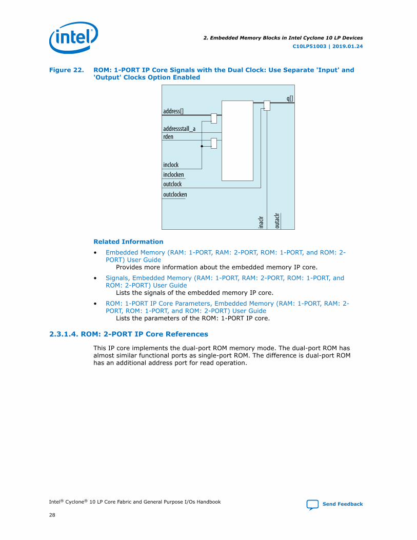
Figure 22. ROM: 1-PORT IP Core Signals with the Dual Clock: Use Separate 'Input' and'Output' Clocks Option Enabled
addressstall_a
outclockoutclocken
q[]
inaclr
address[]
rden
inclockeninclock
outa
clr
Related Information
• Embedded Memory (RAM: 1-PORT, RAM: 2-PORT, ROM: 1-PORT, and ROM: 2-PORT) User Guide
Provides more information about the embedded memory IP core.
• Signals, Embedded Memory (RAM: 1-PORT, RAM: 2-PORT, ROM: 1-PORT, andROM: 2-PORT) User Guide
Lists the signals of the embedded memory IP core.
• ROM: 1-PORT IP Core Parameters, Embedded Memory (RAM: 1-PORT, RAM: 2-PORT, ROM: 1-PORT, and ROM: 2-PORT) User Guide
Lists the parameters of the ROM: 1-PORT IP core.
2.3.1.4. ROM: 2-PORT IP Core References
This IP core implements the dual-port ROM memory mode. The dual-port ROM hasalmost similar functional ports as single-port ROM. The difference is dual-port ROMhas an additional address port for read operation.
2. Embedded Memory Blocks in Intel Cyclone 10 LP Devices
C10LP51003 | 2019.01.24
Intel® Cyclone® 10 LP Core Fabric and General Purpose I/Os Handbook Send Feedback
28

Figure 23. ROM: 2-PORT IP Core Signals with the Single Clock Option Enabled
address_b[]
addressstall_a
clockenable
q_a[]
aclr
address_a[]
addressstall_b
rden_a
rden_b
q_b[]
Figure 24. ROM: 2-PORT IP Core Signals with the Dual Clock: Use Separate 'Input' and'Output' Clocks Option Enabled
address_b[]
addressstall_a
inclockinclockenoutclockoutclocken
q_a[]ou
t_ac
lraddress_a[]
addressstall_b
rden_a
rden_b
q_b[]
2. Embedded Memory Blocks in Intel Cyclone 10 LP Devices
C10LP51003 | 2019.01.24
Send Feedback Intel® Cyclone® 10 LP Core Fabric and General Purpose I/Os Handbook
29

Figure 25. ROM: 2-PORT IP Core Signals with the Dual Clock: Use Separate Clocks for Aand B Ports Option Enabled
address_b[]
addressstall_a
clock_aenable_aclock_benable_b
q_a[]
aclr_
a
address_a[]
addressstall_b
rden_a
rden_b
aclr_
b
q_b[]
Related Information
• Embedded Memory (RAM: 1-PORT, RAM: 2-PORT, ROM: 1-PORT, and ROM: 2-PORT) User Guide
Provides more information about the embedded memory IP core.
• Signals, Embedded Memory (RAM: 1-PORT, RAM: 2-PORT, ROM: 1-PORT, andROM: 2-PORT) User Guide
Lists the signals of the embedded memory IP core.
• ROM: 2-PORT IP Core Parameters, Embedded Memory (RAM: 1-PORT, RAM: 2-PORT, ROM: 1-PORT, and ROM: 2-PORT) User Guide
Lists the parameters of the ROM: 2-PORT IP core.
2.3.1.5. Shift Register (RAM-based) IP Core References
The Shift Register (RAM-based) IP core contains additional features not found in aconventional shift register. You can use the memory blocks as a shift-register block tosave logic cells and routing resources. You can cascade memory blocks to implementlarger shift registers.
Figure 26. Shift Register (RAM-based) IP Core Signals
shift_in[]clockclkenaclr
shiftout[]taps[]
2. Embedded Memory Blocks in Intel Cyclone 10 LP Devices
C10LP51003 | 2019.01.24
Intel® Cyclone® 10 LP Core Fabric and General Purpose I/Os Handbook Send Feedback
30
Related Information
RAM-Based Shift Register (ALTSHIFT_TAPS) IP Core User GuideProvides more information about the RAM-based shift register IP core, itsparameters, and signals.
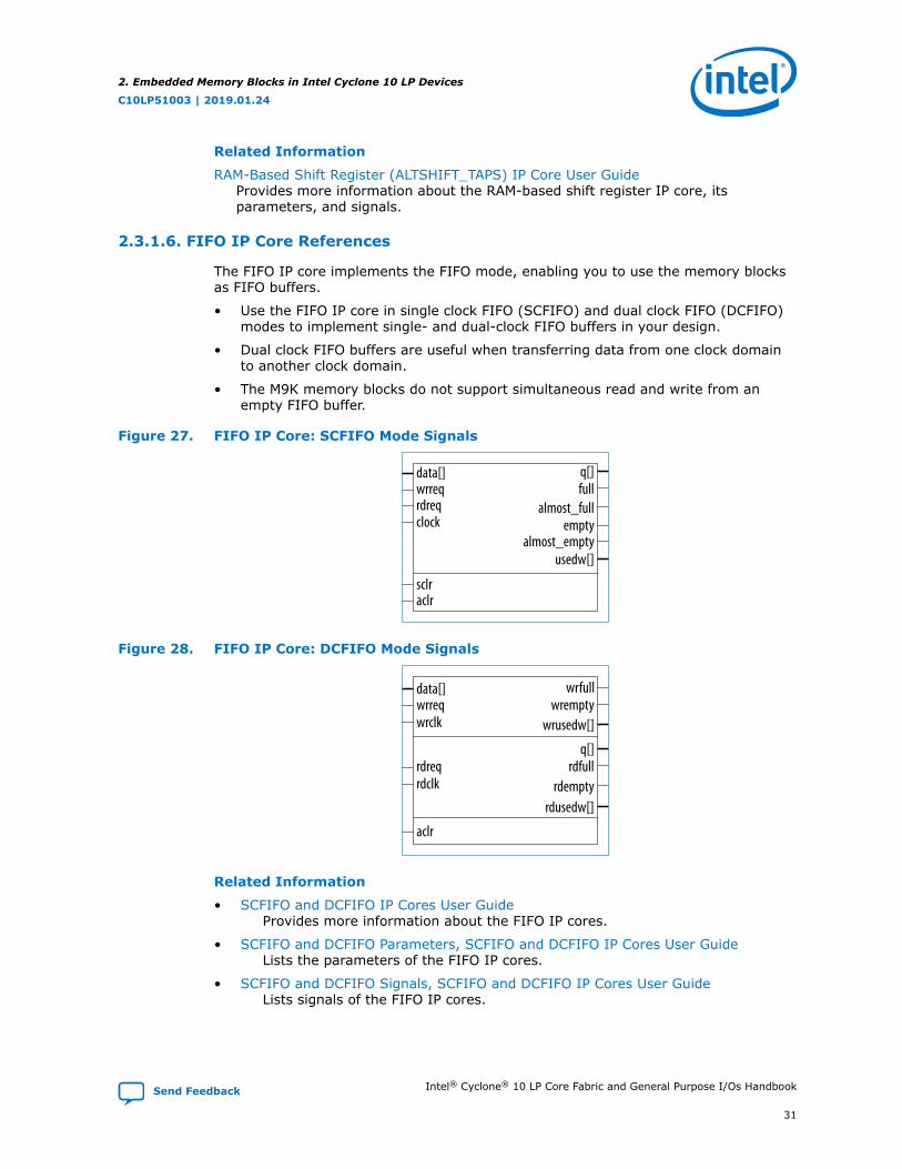
2.3.1.6. FIFO IP Core References
The FIFO IP core implements the FIFO mode, enabling you to use the memory blocksas FIFO buffers.
• Use the FIFO IP core in single clock FIFO (SCFIFO) and dual clock FIFO (DCFIFO)modes to implement single- and dual-clock FIFO buffers in your design.
• Dual clock FIFO buffers are useful when transferring data from one clock domainto another clock domain.
• The M9K memory blocks do not support simultaneous read and write from anempty FIFO buffer.
Figure 27. FIFO IP Core: SCFIFO Mode Signals
data[]wrreqrdreq
q[]full
almost_fullclock empty
almost_emptyusedw[]
sclraclr
Figure 28. FIFO IP Core: DCFIFO Mode Signals
data[]wrreqwrclk
wrfullwrempty
wrusedw[]
rdreqrdclk
q[]rdfull
rdemptyrdusedw[]
aclr
Related Information
• SCFIFO and DCFIFO IP Cores User GuideProvides more information about the FIFO IP cores.
• SCFIFO and DCFIFO Parameters, SCFIFO and DCFIFO IP Cores User GuideLists the parameters of the FIFO IP cores.
• SCFIFO and DCFIFO Signals, SCFIFO and DCFIFO IP Cores User GuideLists signals of the FIFO IP cores.
2. Embedded Memory Blocks in Intel Cyclone 10 LP Devices
C10LP51003 | 2019.01.24
Send Feedback Intel® Cyclone® 10 LP Core Fabric and General Purpose I/Os Handbook
31

2.4. Intel Cyclone 10 LP Embedded Memory Clock Modes
Clock Mode Description Modes
TrueDual-Port
SimpleDual-Port
Single-Port
ROM FIFO
Independent ClockMode
A separate clock is available for the following ports:• Port A—Clock A controls all registers on the port A
side.• Port B—Clock B controls all registers on the port B
side.
Yes — — Yes —
Input/Output ClockMode
• M9K memory blocks can implement input oroutput clock mode for single-port, true dual-port,and simple dual-port memory modes.
• An input clock controls all input registers to thememory block, including data, address,byteena, wren, and rden registers.
• An output clock controls the data-outputregisters.
Yes Yes Yes Yes —
Read or WriteClock Mode
• M9K memory blocks support independent clockenables for both the read and write clocks.
• A read clock controls the data outputs, readaddress, and read enable registers.
• A write clock controls the data inputs, writeaddress, and write enable registers.
— Yes — — Yes
Single-Clock Mode A single clock, together with a clock enable, controlsall registers of the memory block.
Yes Yes Yes Yes Yes
2.4.1. Asynchronous Clear in Clock Modes
In all clock modes, asynchronous clear is available only for output latches and outputregisters. For independent clock mode, this is applicable on port A and port B.
2.4.2. Output Read Data in Simultaneous Read and Write
If you perform a simultaneous read/write to the same address location using the reador write clock mode, the output read data is unknown. If you want the output readdata to be a known value, use single-clock or input/output clock mode and then selectthe appropriate read-during-write behavior in the RAM: 1-PORT and RAM: 2-PORT IPcores.
2.4.3. Independent Clock Enables in Clock Modes
Table 6. Supported Clock Modes for Independent Clock Enables
Clock Mode Description
Read/write Supported for both the read and write clocks.
Independent Supported for the registers of both ports.
2.5. Intel Cyclone 10 LP Embedded Memory Configurations
2. Embedded Memory Blocks in Intel Cyclone 10 LP Devices
C10LP51003 | 2019.01.24
Intel® Cyclone® 10 LP Core Fabric and General Purpose I/Os Handbook Send Feedback
32

2.5.1. Port Width Configurations
The following equation defines the port width configuration: Memory depth (number ofwords) × Width of the data input bus.
• If your port width configuration (either the depth or the width) is more than theamount an internal memory block can support, additional memory blocks (of thesame type) are used. For example, if you configure your M9K as 512 × 36, whichexceeds the supported port width, two 512 × 18 M9Ks are used to implement yourRAM.
• In addition to the supported configuration provided, you can set the memorydepth to a non-power of two, but the actual memory depth allocated can vary. Thevariation depends on the type of resource implemented.
• If the memory is implemented in dedicated memory blocks, setting a non-powerof two for the memory depth reflects the actual memory depth.
• When you implement your memory using dedicated memory blocks, refer to theFitter report to check the actual memory depth.
2.5.2. Memory Configurations for Dual-Port Modes
Table 7. Simple Dual-Port Memory Configurations for M9K BlocksThis table lists the configuration supported simple dual-port memory configuration.
Read Port Write Port
8192 × 1 4096 × 2 2048 × 4 1024 × 8 512 × 16 256 × 32 1024 × 9 512 × 18 256 × 36
8192 × 1 Yes Yes Yes Yes Yes Yes — — —
4096 × 2 Yes Yes Yes Yes Yes Yes — — —
2048 × 4 Yes Yes Yes Yes Yes Yes — — —
1024 × 8 Yes Yes Yes Yes Yes Yes — — —
512 × 16 Yes Yes Yes Yes Yes Yes — — —
256 × 32 Yes Yes Yes Yes Yes Yes — — —
1024 × 9 — — — — — — Yes Yes Yes
512 × 18 — — — — — — Yes Yes Yes
256 × 36 — — — — — — Yes Yes Yes
Table 8. True Dual-Port Memory Configurations for M9K BlocksThis table lists the configuration supported true dual-port memory configuration.
Read Port Write Port
8192 × 1 4096 × 2 2048 × 4 1024 × 8 512 × 16 1024 × 9 512 × 18
8192 × 1 Yes Yes Yes Yes Yes — —
4096 × 2 Yes Yes Yes Yes Yes — —
2048 × 4 Yes Yes Yes Yes Yes — —
1024 × 8 Yes Yes Yes Yes Yes — —
continued...
2. Embedded Memory Blocks in Intel Cyclone 10 LP Devices
C10LP51003 | 2019.01.24
Send Feedback Intel® Cyclone® 10 LP Core Fabric and General Purpose I/Os Handbook
33

Read Port Write Port
8192 × 1 4096 × 2 2048 × 4 1024 × 8 512 × 16 1024 × 9 512 × 18
512 × 16 Yes Yes Yes Yes Yes — —
1024 × 9 — — — — — Yes Yes
512 × 18 — — — — — Yes Yes
2.5.3. Maximum Block Depth Configuration
The Set the maximum block depth parameter allows you to set the maximum blockdepth of the dedicated memory block you use. You can slice the memory block to yourdesired maximum block depth. For example, the capacity of an M9K block is 9,216bits, and the default memory depth is 8K, in which each address is capable of storing1 bit (8K × 1). If you set the maximum block depth to 512, the M9K block is sliced toa depth of 512 and each address is capable of storing up to 18 bits (512 × 18).
Use this parameter to save power usage in your devices and to reduce the totalnumber of memory blocks used. However, this parameter might increase the numberof LEs and affects the design performance.
When the RAM is sliced shallower, the dynamic power usage decreases. However, for aRAM block with a depth of 256, the power used by the extra LEs starts to outweighthe power gain achieved by shallower slices.
The maximum block depth must be in a power of two, and the valid values varyamong different dedicated memory blocks.
This table lists the valid range of maximum block depth for M9K memory blocks.
Table 9. Valid Range of Maximum Block Depth for M9K Memory Blocks
Memory Block Valid Range
M9K 256 - 8K. The maximum block depth must be in a power of two.
The IP parameter editor prompts an error message if you enter an invalid value for themaximum block depth. Intel recommends that you set the value of the Set themaximum block depth parameter to Auto if you are unsure of the appropriatemaximum block depth to set or the setting is not important for your design. The Autosetting enables the Compiler to select the maximum block depth with the appropriateport width configuration for the type of internal memory block of your memory.
2.6. Intel Cyclone 10 LP Embedded Memory Design Consideration
There are several considerations that require your attention to ensure the success ofyour designs.
2.6.1. Implement External Conflict Resolution
In the true dual-port RAM mode, you can perform two write operations to the samememory location. However, the memory blocks do not have internal conflict resolutioncircuitry.
To avoid unknown data being written to the address, implement external conflictresolution logic to the memory block.
2. Embedded Memory Blocks in Intel Cyclone 10 LP Devices
C10LP51003 | 2019.01.24
Intel® Cyclone® 10 LP Core Fabric and General Purpose I/Os Handbook Send Feedback
34

2.6.2. Customize Read-During-Write Behavior
Customize the read-during-write behavior of the memory blocks to suit your designrequirements.
Figure 29. Difference Between the Two Types of Read-during-Write Operations —SamePort and Mixed Port.
Port Adata in
Port Bdata in
Port Adata out
Port Bdata out
Mixed-portdata flowSame-portdata flow
FPGA Device
Related Information
Embedded Memory (RAM: 1-PORT, RAM: 2-PORT, ROM: 1-PORT, and ROM: 2-PORT)User Guide
Provides more information about the supported modes, signals, and parameters ofthe embedded memory IP cores that support the M9K blocks in the Intel Cyclone10 LP devices.
2.6.2.1. Same-Port Read-During-Write Mode
The same-port read-during-write mode applies to a single-port RAM or the same portof a true dual-port RAM.
Table 10. Output Modes for Embedded Memory Blocks in Same-Port Read-During-WriteModeThis table lists the available output modes if you select the embedded memory blocks in the same-port read-during-write mode.
Output Mode Description
"new data"(flow-through)
The new data is available on the rising edge of the same clock cycle on which the new data iswritten.When using New Data mode together with byte enable, you can control the output of the RAM:• When byte enable is high, the data written into the memory passes to the output (flow-
through).• When byte enable is low, the masked-off data is not written into the memory and the old
data in the memory appears on the outputs.Therefore, the output can be a combination of new and old data determined by byteena.
"don't care" The RAM outputs reflect the old data at that address before the write operation proceeds.
2. Embedded Memory Blocks in Intel Cyclone 10 LP Devices
C10LP51003 | 2019.01.24
Send Feedback Intel® Cyclone® 10 LP Core Fabric and General Purpose I/Os Handbook
35

Figure 30. Same-Port Read-During-Write: New Data Mode
clk_a
wren_a
address_a
data_a
rden_a
q_a (asynch)
a0 a1
A B C D E F
A B C D E F
Figure 31. Same Port Read-During-Write: Old Data Mode
clk_a
wren_a
address_a
data_a
rden_a
q_a (asynch)
a0 a1
A B C D E F
a0(old data) a1(old data)A B D E
2.6.2.2. Mixed-Port Read-During-Write Mode
The mixed-port read-during-write mode applies to simple and true dual-port RAMmodes where two ports perform read and write operations on the same memoryaddress using the same clock—one port reading from the address, and the other portwriting to it.
Table 11. Output Modes for RAM in Mixed-Port Read-During-Write Mode
Output Mode Description
"old data" A read-during-write operation to different ports causes the RAM output to reflect the “olddata” value at the particular address.
"don't care" The RAM outputs “don’t care” or “unknown” value.
2. Embedded Memory Blocks in Intel Cyclone 10 LP Devices
C10LP51003 | 2019.01.24
Intel® Cyclone® 10 LP Core Fabric and General Purpose I/Os Handbook Send Feedback
36

Figure 32. Mixed-Port Read-During-Write: Old Data Mode
a b
a (old data) b (old data)
clk_a&b
wren_a
address_a
q_b (asynch)
rden_b
a baddress_b
data_a A B C D E F
A B D E
In Don't Care mode, the old data is replaced with “Don't Care”.
2.6.2.2.1. Mixed-Port Read-During-Write Operation with Dual Clocks
For mixed-port read-during-write operation with dual clocks, the relationship betweenthe clocks determines the output behavior of the memory.
If You... ...Then
Use the same clock for the two clocks The output is the old data from the address location.
Use different clocks The output is unknown during the mixed-port read-during-writeoperation. This unknown value may be the old or new data at theaddress location, depending on whether the read happens before orafter the write.
2.6.3. Consider Power-Up State and Memory Initialization
Consider the power-up state of the different types of memory blocks if you aredesigning logic that evaluates the initial power-up values.
Table 12. Initial Power-Up Values of Embedded Memory Blocks
Memory Type Output Registers Power Up Value
M9K Used Zero (cleared)
Bypassed Zero (cleared)
By default, the Intel Quartus Prime software initializes the RAM cells to zero unlessyou specify a .mif.
All memory blocks support initialization with a .mif. You can create .mif files in theIntel Quartus Prime software and specify their use with the RAM IP when youinstantiate a memory in your design. Even if a memory is preinitialized (for example,using a .mif), it still powers up with its output cleared. Only the subsequent read afterpower up outputs the preinitialized values.
2. Embedded Memory Blocks in Intel Cyclone 10 LP Devices
C10LP51003 | 2019.01.24
Send Feedback Intel® Cyclone® 10 LP Core Fabric and General Purpose I/Os Handbook
37

2.6.4. Control Clocking to Reduce Power Consumption
Reduce AC power consumption in your design by controlling the clocking of eachmemory block:
• Use the read-enable signal to ensure that read operations occur only whennecessary. If your design does not require read-during-write, you can reduce yourpower consumption by deasserting the read-enable signal during write operations,or during the period when no memory operations occur.
• Use the Intel Quartus Prime software to automatically place any unused memoryblocks in low-power mode to reduce static power.
• Create independent clock enable for different input and output registers to controlthe shut down of a particular register for power saving purposes. From theparameter editor, click More Options (beside the clock enable option) to set theavailable independent clock enable that you prefer.
2.6.5. Selecting Read-During-Write Output Choices
• Single-port RAM supports only same-port read-during-write. The clock mode mustbe either single clock mode or input/output clock mode.
• Simple dual-port RAM supports only mixed-port read-during-write. The clock modemust be either single clock mode, or input/output clock mode.
• True dual-port RAM supports same port read-during-write and mixed-port read-during-write:
— For same port read-during-write, the clock mode must be either single clockmode, input/output clock mode, or independent clock mode.
— For mixed port read-during-write, the clock mode must be either single clockmode, or input/output clock mode.
Note: If you are not concerned about the output when read-during-write occurs and want toimprove performance, select Don't Care. Selecting Don't Care increases theflexibility in the type of memory block being used if you do not assign block type whenyou instantiate the memory block.
Table 13. Output Choices for the Same-Port and Mixed-Port Read-During-Write
Memory Block Single-Port RAM Simple Dual-PortRAM
True Dual-Port RAM
Same-Port Read-During-Write
Mixed-Port Read-During-Write
Same-Port Read-During-Write
Mixed-Port Read-During-Write
M9K • Don’t Care• New Data• Old Data
• Old Data• Don’t Care
• New Data• Old Data
• Old Data• Don’t Care
2.7. Embedded Memory Blocks in Intel Cyclone 10 LP DevicesRevision History
Date Version Changes
May 2017 2017.05.08 Initial release.
2. Embedded Memory Blocks in Intel Cyclone 10 LP Devices
C10LP51003 | 2019.01.24
Intel® Cyclone® 10 LP Core Fabric and General Purpose I/Os Handbook Send Feedback
38

3. Embedded Multipliers in Intel Cyclone 10 LP DevicesThe Intel Cyclone 10 LP devices include a combination of on-chip resources andexternal interfaces that help increase performance, reduce system cost, and lower thepower consumption of digital signal processing (DSP) systems.
The Intel Cyclone 10 LP devices, either alone or as DSP device coprocessors, improvesthe price-to-performance ratios of DSP systems. The Intel Cyclone 10 LP devices areoptimized for applications that benefit from an abundance of parallel processingresources, which include video and image processing, intermediate frequency (IF)modems used in wireless communications systems, and multi-channelcommunications and video systems.
3.1. Embedded Multiplier Block Overview
Each embedded multiplier block in Intel Cyclone 10 LP devices supports one individual18 × 18-bit multiplier or two individual 9 × 9-bit multipliers.
For multiplications greater than 18 x 18, the Intel Quartus Prime software cascadesthe multiplier blocks to form wider or deeper logic structures. There are no restrictionson the data width of the multiplier but the greater the data width, the slower themultiplication process.
You can control the operation of the embedded multiplier blocks using the followingoptions:
• Parameterize the relevant IP cores with the Quartus Prime parameter editor
• Infer the multipliers directly with VHDL or Verilog HDL
C10LP51003 | 2019.01.24
Send Feedback
Intel Corporation. All rights reserved. Intel, the Intel logo, Altera, Arria, Cyclone, Enpirion, MAX, Nios, Quartusand Stratix words and logos are trademarks of Intel Corporation or its subsidiaries in the U.S. and/or othercountries. Intel warrants performance of its FPGA and semiconductor products to current specifications inaccordance with Intel's standard warranty, but reserves the right to make changes to any products and servicesat any time without notice. Intel assumes no responsibility or liability arising out of the application or use of anyinformation, product, or service described herein except as expressly agreed to in writing by Intel. Intelcustomers are advised to obtain the latest version of device specifications before relying on any publishedinformation and before placing orders for products or services.*Other names and brands may be claimed as the property of others.
ISO9001:2015Registered

Figure 33. Embedded Multipliers Arranged in Columns with Adjacent LABS
EmbeddedMultiplier
EmbeddedMultiplier
Column
1 LABRow
Additionally, you can implement soft multipliers by using the M9K memory blocks aslook-up tables (LUTs). The LUTs contain partial results from the multiplication of inputdata with coefficients that implements variable depth and width high-performance softmultipliers. Using soft multipliers increases the number of available multipliers in thedevice.
Related Information
• LPM_MULT (Multiplier) IP CoreProvides more information about the LPM_MULT IP core that implements amultiplier to multiply two input data values to produce a product as an output.
• ALTMULT_ACCUM (Multiply-Accumulate) IP CoreProvides more information about the ALTMULT_ACCUM IP core that allows youto implement a multiplier-accumulator.
• ALTMULT_ADD (Multiply-Adder) IP CoreProvides more information about the ALTMULT_ADD IP core that allows you toimplement a multiplier-adder.
• ALTMULT_COMPLEX (Complex Multiplier) IP CoreProvides more information about the ALTMULT_COMPLEX IP core thatimplements the multiplication of two complex numbers in canonical andconventional modes.
• ALTMEMMULT (Memory-based Constant Coefficient Multiplier) IP CoreProvides more information about the ALTMEMMULT IP core that you can use tocreate soft multipliers using the M9K memory blocks.
3. Embedded Multipliers in Intel Cyclone 10 LP Devices
C10LP51003 | 2019.01.24
Intel® Cyclone® 10 LP Core Fabric and General Purpose I/Os Handbook Send Feedback
40

3.2. Multipliers Resources in Intel Cyclone 10 LP Devices
Table 14. Number of Multipliers in Intel Cyclone 10 LP Devices
Device Embedded Multipliers Multipliers by Type
9 × 9(1) 18 × 18(1) Embedded Soft (16 × 16)(2) Total(Embedded +
Soft)(3)
10CL006 30 15 15 30 45
10CL010 46 23 23 46 69
10CL016 112 56 56 56 112
10CL025 132 66 66 66 132
10CL040 252 126 126 126 252
10CL055 308 156 156 260 416
10CL080 488 244 244 305 549
10CL120 576 288 288 432 720
3.3. Embedded Multipliers Architecture
Each embedded multiplier consists of the following elements:
• Multiplier stage
• Input and output registers
• Input and output interfaces
(1) These columns show the number of 9 x 9 or 18 x 18 multipliers for each device. The totalnumber of multipliers for each device is not the sum of all the multipliers.
(2) Soft multipliers are implemented in sum of multiplication mode. M9K memory blocks areconfigured with 18-bit data widths to support 16-bit coefficients. The sum of the coefficientsrequires 18-bits of resolution to account for overflow.
(3) The total number of multipliers may vary, depending on the multiplier mode you use.
3. Embedded Multipliers in Intel Cyclone 10 LP Devices
C10LP51003 | 2019.01.24
Send Feedback Intel® Cyclone® 10 LP Core Fabric and General Purpose I/Os Handbook
41

Figure 34. Multiplier Block Architecture
CLRN
D QENA
Data A
Data B
aclrclock
ena
signasignb
CLRN
D QENA
CLRN
D QENA Data Out
Embedded Multiplier Block
OutputRegisterInput
Register
3.3.1. Input Register
Depending on the operational mode of the multiplier, you can send each multiplierinput signal into either one of the following:
• An input register
• The multiplier in 9- or 18-bit sections
Each multiplier input signal can be sent through a register independently of otherinput signals. For example, you can send the multiplier Data A signal through aregister and send the Data B signal directly to the multiplier.
The following control signals are available to each input register in the embeddedmultiplier:
• Clock
• Clock enable
• Asynchronous clear
All input and output registers in a single embedded multiplier are fed by the sameclock, clock enable, and asynchronous clear signals.
3.3.2. Multiplier Stage
The multiplier stage of an embedded multiplier block supports 9 × 9 or 18 × 18multipliers and other multipliers in between these configurations. Depending on thedata width or operational mode of the multiplier, a single embedded multiplier canperform one or two multiplications in parallel.
Each multiplier operand is a unique signed or unsigned number. Two signals, signaand signb, control an input of a multiplier and determine if the value is signed orunsigned. If the signa signal is high, the Data A operand is a signed number. If thesigna signal is low, the Data A operand is an unsigned number.
3. Embedded Multipliers in Intel Cyclone 10 LP Devices
C10LP51003 | 2019.01.24
Intel® Cyclone® 10 LP Core Fabric and General Purpose I/Os Handbook Send Feedback
42

The following table lists the sign of the multiplication results for the various operandsign representations. The results of the multiplication are signed if any one of theoperands is a signed value.
Data A Data B Result
signa Value Logic Level signb Value Logic Level
Unsigned Low Unsigned Low Unsigned
Unsigned Low Signed High Signed
Signed High Unsigned Low Signed
Signed High Signed High Signed
Each embedded multiplier block has only one signa and one signb signal to controlthe sign representation of the input data to the block. If the embedded multiplier blockhas two 9 × 9 multipliers, the Data A input of both multipliers share the same signasignal, and the Data B input of both multipliers share the same signb signal.
You can dynamically change the signa and signb signals to modify the signrepresentation of the input operands at run time. You can send the signa and signbsignals through a dedicated input register. The multiplier offers full precision,regardless of the sign representation.
When the signa and signb signals are unused, the Intel Quartus Prime software setsthe multiplier to perform unsigned multiplication by default.
3.3.3. Output Register
You can register the embedded multiplier output using output registers in either 18- or36-bit sections. This depends on the operational mode of the multiplier. The followingcontrol signals are available for each output register in the embedded multiplier:
• Clock
• Clock enable
• Asynchronous clear
All input and output registers in a single embedded multiplier are fed by the sameclock, clock enable, and asynchronous clear signals.
3.4. Embedded Multipliers Operational Modes
You can use an embedded multiplier block in one of two operational modes, dependingon the application needs:
• One 18-bit x 18-bit multiplier
• Up to two 9-bit x 9-bit independent multipliers
You can also use embedded multipliers of the Intel Cyclone 10 LP devices toimplement multiplier adder and multiplier accumulator functions. The multiplierportion of the function is implemented using embedded multipliers. The adder oraccumulator function is implemented in logic elements (LEs).
3. Embedded Multipliers in Intel Cyclone 10 LP Devices
C10LP51003 | 2019.01.24
Send Feedback Intel® Cyclone® 10 LP Core Fabric and General Purpose I/Os Handbook
43

3.4.1. 18-Bit Multipliers
You can configure each embedded multiplier to support a single 18 x 18 multiplier forinput widths of 10 to 18 bits.
The following figure shows the embedded multiplier configured to support an 18-bitmultiplier.
Figure 35. 18-Bit Multiplier Mode
CLRN
D QENA
Data A [17..0]
Data B [17..0]
aclrclock
ena
signasignb
CLRN
D QENA
CLRN
D QENA Data Out [35..0]
18 x 18 Multiplier
Embedded Multiplier
All 18-bit multiplier inputs and results are independently sent through registers. Themultiplier inputs can accept signed integers, unsigned integers, or a combination ofboth. Also, you can dynamically change the signa and signb signals and send thesesignals through dedicated input registers.
3.4.2. 9-Bit Multipliers
You can configure each embedded multiplier to support two 9 × 9 independentmultipliers for input widths of up to 9 bits.
The following figure shows the embedded multiplier configured to support two 9-bitmultipliers.
3. Embedded Multipliers in Intel Cyclone 10 LP Devices
C10LP51003 | 2019.01.24
Intel® Cyclone® 10 LP Core Fabric and General Purpose I/Os Handbook Send Feedback
44

Figure 36. 9-Bit Multiplier Mode
CLRN
D QENA
Data A 0 [8..0]
Data B 0 [8..0]
aclrclock
ena
signasignb
CLRN
D QENA
CLRN
D QENA Data Out 0 [17..0]
9 x 9 Multiplier
Embedded Multiplier
CLRN
D QENA
Data A 1 [8..0]
Data B 1 [8..0]
CLRN
D QENA
CLRN
D QENA Data Out 1 [17..0]
9 x 9 Multiplier
All 9-bit multiplier inputs and results are independently sent through registers. Themultiplier inputs can accept signed integers, unsigned integers, or a combination ofboth.
Each embedded multiplier block has only one signa and one signb signal to controlthe sign representation of the input data to the block. If the embedded multiplier blockhas two 9 × 9 multipliers the following applies:
• The Data A input of both multipliers share the same signa signal
• The Data B input of both multipliers share the same signb signal
3. Embedded Multipliers in Intel Cyclone 10 LP Devices
C10LP51003 | 2019.01.24
Send Feedback Intel® Cyclone® 10 LP Core Fabric and General Purpose I/Os Handbook
45

3.5. Embedded Multipliers in Intel Cyclone 10 LP Devices RevisionHistory
Date Version Changes
May 2017 2017.05.08 Initial release.
3. Embedded Multipliers in Intel Cyclone 10 LP Devices
C10LP51003 | 2019.01.24
Intel® Cyclone® 10 LP Core Fabric and General Purpose I/Os Handbook Send Feedback
46

4. Clock Networks and PLLs in Intel Cyclone 10 LP DevicesThis chapter describes the hierarchical clock networks and phase-locked loops (PLLs)with advanced features in the Intel Cyclone 10 LP devices. It includes details about theability to reconfigure the PLL counter clock frequency and phase shift in real time,allowing you to sweep PLL output frequencies and dynamically adjust the output clockphase shift.
The Intel Quartus Prime software enables the PLLs and their features without externaldevices.
4.1. Clock Networks
The Intel Cyclone 10 LP device provides up to 16 dedicated clock pins (CLK[15..0])that can drive up to 20 global clocks (GCLKs). Intel Cyclone 10 LP devices supportthree dedicated clock pins on the left side and four dedicated clock pins on the top,right, and bottom sides of the device except 10CL006 and 10CL010 devices. 10CL006and 10CL010 devices only support three dedicated clock pins on the left side and fourdedicated clock pins on the right side of the device.
Related Information
Intel Cyclone 10 LP Maximum Resources, Intel Cyclone 10 LP Device OverviewProvides more information about the number of GCLK networks in each devicedensity.
4.1.1. GCLK Network
GCLKs drive throughout the entire device, feeding all device quadrants. All resourcesin the device (I/O elements, logic array blocks (LABs), dedicated multiplier blocks, andM9K memory blocks) can use GCLKs as clock sources. Use these clock networkresources for control signals, such as clock enables and clears fed by an external pin.Internal logic can also drive GCLKs for internally generated GCLKs and asynchronousclears, clock enables, or other control signals with high fan-out.
4.1.2. GCLK Network Sources
Table 15. Intel Cyclone 10 LP Clock Sources Connectivity to the GCLK Networks10CL006 and 10CL010 devices only have GCLK networks 0 to 9.
GCLK Network Clock Sources GCLK Networks
CLK0/DIFFCLK_0p GCLK[0,2,4]
CLK1/DIFFCLK_0n GCLK[1,2]
CLK2/DIFFCLK_1p GCLK[1,3,4]
continued...
C10LP51003 | 2019.01.24
Send Feedback
Intel Corporation. All rights reserved. Intel, the Intel logo, Altera, Arria, Cyclone, Enpirion, MAX, Nios, Quartusand Stratix words and logos are trademarks of Intel Corporation or its subsidiaries in the U.S. and/or othercountries. Intel warrants performance of its FPGA and semiconductor products to current specifications inaccordance with Intel's standard warranty, but reserves the right to make changes to any products and servicesat any time without notice. Intel assumes no responsibility or liability arising out of the application or use of anyinformation, product, or service described herein except as expressly agreed to in writing by Intel. Intelcustomers are advised to obtain the latest version of device specifications before relying on any publishedinformation and before placing orders for products or services.*Other names and brands may be claimed as the property of others.
ISO9001:2015Registered

GCLK Network Clock Sources GCLK Networks
CLK3/DIFFCLK_1n GCLK[0,3]
CLK4/DIFFCLK_2p GCLK[5,7,9]
CLK5/DIFFCLK_2n GCLK[6,7]
CLK6/DIFFCLK_3p GCLK[6,8,9]
CLK7/DIFFCLK_3n GCLK[5,8]
CLK8/DIFFCLK_5n (4) GCLK[10,12,14]
CLK9/DIFFCLK_5p (4) GCLK[11,12]
CLK10/DIFFCLK_4n (4) GCLK[11,13,14]
CLK11/DIFFCLK_4p (4) GCLK[10,13]
CLK12/DIFFCLK_7n (4) GCLK[15,17,19]
CLK13/DIFFCLK_7p (4) GCLK[16,17]
CLK14/DIFFCLK_6n (4) GCLK[16,18,19]
CLK15/DIFFCLK_6p (4) GCLK[15,18]
PLL_1_C0 (5) GCLK[0,3]
PLL_1_C1 (5) GCLK[1,4]
PLL_1_C2 (5) GCLK[0,2]
PLL_1_C3 (5) GCLK[1,3]
PLL_1_C4 (5) GCLK[2,4]
PLL_2_C0 (5) GCLK[5,8]
PLL_2_C1 (5) GCLK[6,9]
PLL_2_C2 (5) GCLK[5,7]
PLL_2_C3 (5) GCLK[6,8]
PLL_2_C4 (5) GCLK[7,9]
PLL_3_C0 GCLK[10,13]
PLL_3_C1 GCLK[11,14]
PLL_3_C2 GCLK[10,12]
PLL_3_C3 GCLK[11,13]
PLL_3_C4 GCLK[12,14]
PLL_4_C0 GCLK[15,18]
PLL_4_C1 GCLK[16,19]
PLL_4_C2 GCLK[15,17]
continued...
(4) These pins apply to all Intel Cyclone 10 LP devices except10CL006 and 10CL010 devices.
(5) 10CL006 and 10CL010 devices only have PLL_1 and PLL_2.
4. Clock Networks and PLLs in Intel Cyclone 10 LP Devices
C10LP51003 | 2019.01.24
Intel® Cyclone® 10 LP Core Fabric and General Purpose I/Os Handbook Send Feedback
48

GCLK Network Clock Sources GCLK Networks
PLL_4_C3 GCLK[16,18]
PLL_4_C4 GCLK[17,19]
DPCLK0 GCLK[0]
DPCLK1 GCLK[1]
DPCLK7 (6), CDPCLK0, or CDPCLK7 (4) (7) GCLK[2]
DPCLK2 (6), CDPCLK1, or CDPCLK2 (4) (7) GCLK[3,4]
DPCLK5 (6), DPCLK7 (4) GCLK[5]
DPCLK4 (6), DPCLK6 (4) GCLK[6]
DPCLK6 (6), CDPCLK5, or CDPCLK6 (4) (7) GCLK[7]
DPCLK3 (6), CDPCLK4, or CDPCLK3 (4) (7) GCLK[8,9]
DPCLK8 GCLK[10]
DPCLK11 GCLK[11]
DPCLK9 GCLK[12]
DPCLK10 GCLK[13,14]
DPCLK5 GCLK[15]
DPCLK2 GCLK[16]
DPCLK4 GCLK[17]
DPCLK3 GCLK[18,19]
Related Information
Clock and PLL Pins, Intel Cyclone 10 LP Device Family Pin Connection GuidelinesProvides more information about the clock and PLL pins connections.
4.1.3. Clock Control Block
The clock control block drives the GCLKs. Clock control blocks are located on each sideof the device, close to the dedicated clock input pins. GCLKs are optimized forminimum clock skew and delay.
(6) This pin applies only to 10CL006 and 10CL010 devices.
(7) Only one of the two CDPCLK pins can feed the clock control block. You can use the other pin asa regular I/O pin.
4. Clock Networks and PLLs in Intel Cyclone 10 LP Devices
C10LP51003 | 2019.01.24
Send Feedback Intel® Cyclone® 10 LP Core Fabric and General Purpose I/Os Handbook
49

Table 16. Clock Control Block Inputs
Input Description
Dedicated clock input pins Dedicated clock input pins can drive clocks or global signals, such assynchronous and asynchronous clears, presets, or clock enables ontogiven GCLKs.
Dual-purpose clock (DPCLK and CDPCLK) I/Oinput
DPCLK and CDPCLK pins are bidirectional dual function pins that areused for high fan-out control signals, such as protocol signals, TRDY andIRDY signals for PCI via the GCLK. Clock control blocks that have inputsdriven by dual-purpose clock I/O pins cannot drive PLL inputs.
PLL outputs PLL counter outputs can drive the GCLK.
Internal logic You can drive the GCLK through logic array routing to enable the internallogic elements (LEs) to drive a high fan-out, low-skew signal path. Clockcontrol blocks that have inputs driven by internal logic cannot drive PLLinputs.
In Intel Cyclone 10 LP devices, dedicated clock input pins, PLL counter outputs, dual-purpose clock I/O inputs, and internal logic can all feed the clock control block foreach GCLK. The output from the clock control block in turn feeds the correspondingGCLK. The GCLK can drive the PLL input if the clock control block inputs are outputs ofanother PLL or dedicated clock input pins.
The maximum number of clock control blocks per Intel Cyclone 10 LP device is 20.
The control block has two functions:
• Dynamic GCLK clock source selection (not applicable for DPCLK, CDPCLK, andinternal logic input)
• GCLK network power down (dynamic enable and disable)
Figure 37. Clock Control BlockEach PLL generates five clock outputs through the c[4..0] counters. Two of these clocks can drive the GCLKthrough a clock control block.
clkswitch (1)
Static Clock Select (3)
Static ClockSelect (3)
Internal Logic
Clock Control Block
DPCLK
clkselect[1..0] (2) Internal Logic (4)
inclk1inclk0
CLK[n + 3]CLK[n + 2]CLK[n + 1]CLK[n]
fIN
C0C1C2PLL
GlobalClock
Enable/Disable
C3C4
Notes:(1) The clkswitch signal can either be set through the configuration file or dynamically set when using the manual PLL switchover feature. The output of the multiplexer is the input clock (fIN) for the PLL.(2) The clkselect[1..0] signals are fed by internal logic and are used to dynamically select the clock source for the GCLK when the device is in user mode.(3) The static clock select signals are set in the configuration file. Therefore, dynamic control when the device is in user mode is not feasible.(4) You can use internal logic to enable or disable the GCLK in user mode.
4. Clock Networks and PLLs in Intel Cyclone 10 LP Devices
C10LP51003 | 2019.01.24
Intel® Cyclone® 10 LP Core Fabric and General Purpose I/Os Handbook Send Feedback
50

Related Information
• GCLK Network Clock Source Generation on page 51Shows the clock control block locations.
• Clock Control Block (ALTCLKCTRL) IP Core User GuideProvides more information about the clock control block in the Intel QuartusPrime software.
4.1.4. GCLK Network Clock Source Generation
Figure 38. Clock Networks and Clock Control Block Locations in Intel Cyclone 10 LPDevices
PLL_1PLL_4
PLL_2PLL_3
20
20
20
20
4
4
4
44
4
4
4
2
2
2
2
2 2
2 2
5
5
5
5
(2)(2)
(2) (2)
CDPCLK7
CDPCLK0
CDPCLK1
DPCLK1
DPCLK[11.10] DPCLK[9..8]
CLK[11..8] CDPCLK6
DPCLK0
CLK[3..0]
GCLK[19..0]
GCLK[19..0]
CDPCLK5
DPCLK7
CLK[7..4]
DPCLK6
CDPCLK4
CDPCLK2
DPCLK[3..2]
CLK[15..12]
DPCLK[5..4]
CDPCLK3
4
4
4
4
(3)
(3)
(3)
(4)
(4)(3)
Clock Control Block (1)
Clock Control Block (1)
Clock Control Block (1)
Clock Control Block (1)
Notes:(1) There are five clock control blocks on each side.(2) Only one of the corner CDPCLK pins in each corner can feed the clock control block at a time. You can use the other CDPCLK pins as general-purpose I/O (GPIO) pins.(3) Dedicated clock pins can feed into this PLL. However, these paths are not fully compensated.(4) PLL_3 and PLL_4 are not available in 10CL006 and 10CL010 devices.
4. Clock Networks and PLLs in Intel Cyclone 10 LP Devices
C10LP51003 | 2019.01.24
Send Feedback Intel® Cyclone® 10 LP Core Fabric and General Purpose I/Os Handbook
51

The inputs to the five clock control blocks on each side of the Intel Cyclone 10 LPdevice must be chosen from among the following clock sources:
• Three or four clock input pins, depending on the specific device
• Five PLL counter outputs
• Two DPCLK pins and two CDPCLK pins from both the left and right sides and fourDPCLK pins from both the top and bottom
• Five signals from internal logic
From the clock sources listed above, only two clock input pins, two PLL clock outputs,one DPCLK or CDPCLK pin, and one source from internal logic can drive into any givenclock control block.
Out of these six inputs to any clock control block, the two clock input pins and two PLLoutputs are dynamically selected to feed a GCLK. The clock control block supportsstatic selection of the signal from internal logic.
Figure 39. Clock Control Blocks on Each Side of Intel Cyclone 10 LP DeviceThe left and right sides of the device have two DPCLK pins; the top and bottom of the device have four DPCLKpins.
5GCLK
Clock Input Pins 3 or 4
DPCLK
Internal Logic
ClockControlBlock
5PLL Outputs
5
2 or 4 CDPCLK
2
Five Clock ControlBlocks on Each Side
of the Device
Related Information
Clock Control Block on page 49
4.1.5. GCLK Network Power Down
You can disable an Intel Cyclone 10 LP device’s GCLK (power down) using both staticand dynamic approaches. In the static approach, configuration bits are set in theconfiguration file generated by the Intel Quartus Prime software, which automaticallydisables unused GCLKs. The dynamic clock enable or disable feature allows internallogic to control clock enable or disable the GCLKs in Intel Cyclone 10 LP devices.
When a clock network is disabled, all the logic fed by the clock network is in an off-state, thereby reducing the overall power consumption of the device. This function isindependent of the PLL and is applied directly on the clock network.
You can set the input clock sources and the clkena signals for the GCLK multiplexersthrough the Intel Quartus Prime software using the ALTCLKCTRL IP core.
4. Clock Networks and PLLs in Intel Cyclone 10 LP Devices
C10LP51003 | 2019.01.24
Intel® Cyclone® 10 LP Core Fabric and General Purpose I/Os Handbook Send Feedback
52

Related Information
• Clock Control Block on page 49
• Clock Control Block (ALTCLKCTRL) IP Core User GuideProvides more information about the clock control block in the Intel QuartusPrime software.
4.1.6. Clock Enable Signals
Intel Cyclone 10 LP devices support clkena signals at the GCLK network level. Thisallows you to gate-off the clock even when a PLL is used. Upon re-enabling the outputclock, the PLL does not need a resynchronization or re-lock period because the circuitgates off the clock at the clock network level. In addition, the PLL can remain lockedindependent of the clkena signals because the loop-related counters are notaffected.
Figure 40. clkena ImplementationThis figure shows the implementation of the clkena signal with a single register. The clkena circuitrycontrolling the output C0 of the PLL to an output pin is implemented with two registers instead of a singleregister.
clkena clkena_out
clk_out
clkinD Q
Figure 41. Example Waveform of clkena Implementation with Output EnableThis figure shows the waveform example for a clock output enable. The clkena signal is sampled on the fallingedge of the clock (clkin). This feature is useful for applications that require low power or sleep mode.
clkin
clkena
clk_out
The clkena signal can also disable clock outputs if the system is not tolerant tofrequency overshoot during PLL resynchronization.
4. Clock Networks and PLLs in Intel Cyclone 10 LP Devices
C10LP51003 | 2019.01.24
Send Feedback Intel® Cyclone® 10 LP Core Fabric and General Purpose I/Os Handbook
53

Intel recommends using the clkena signals when switching the clock source to thePLLs or the GCLK. The recommended sequence is:
1. Disable the primary output clock by de-asserting the clkena signal.
2. Switch to the secondary clock using the dynamic select signals of the clock controlblock.
3. Allow some clock cycles of the secondary clock to pass before reasserting theclkena signal. The exact number of clock cycles you must wait before enablingthe secondary clock is design-dependent. You can build custom logic to ensureglitch-free transition when switching between different clock sources.
4.2. PLLs in Intel Cyclone 10 LP Devices
Intel Cyclone 10 LP devices only have the general purpose PLLs. The general purposePLLs are used for general-purpose applications in the FPGA fabric and periphery suchas external memory interfaces.
Intel Cyclone 10 LP devices have up to four general purpose PLLs that provide robustclock management and synthesis for device clock management, external system clockmanagement, and high-speed I/O interfaces.
The general I/O pins cannot drive the PLL clock input pins.
Related Information
Intel Cyclone 10 LP Package Plan, Intel Cyclone 10 LP Device OverviewProvides more information about the number of general purpose PLLs in eachdevice density.
4.2.1. PLL Features
Table 17. Intel Cyclone 10 LP PLL Features
Feature Support
C output counters 5
M, N, C counter sizes 1 to 512 (8)
Dedicated clock outputs 1 single-ended or 1 differential
Dedicated clock input pins 4 single-ended or 2 differential
Spread-spectrum input clock tracking Yes (9)
PLL cascading Through GCLK
Source synchronous compensation Yes
No compensation mode Yes
Normal compensation Yes
Zero-delay buffer compensation Yes
continued...
(8) C counters range from 1 through 512 if the output clock uses a 50% duty cycle. For anyoutput clocks using a non-50% duty cycle, the post-scale counters range from 1 through 256.
(9) Only applicable if the input clock jitter is in the input jitter tolerance specifications.
4. Clock Networks and PLLs in Intel Cyclone 10 LP Devices
C10LP51003 | 2019.01.24
Intel® Cyclone® 10 LP Core Fabric and General Purpose I/Os Handbook Send Feedback
54

Feature Support
Phase shift resolution Down to 96 ps increments (10)
Programmable duty cycle Yes
Output counter cascading Yes
Input clock switchover Yes
User mode reconfiguration Yes
Loss of lock detection Yes
4.2.2. PLL Architecture
Figure 42. Intel Cyclone 10 LP PLL Block DiagramEach clock source can come from any of the four clock pins located on the same side of the device as the PLL.
ClockSwitchover
Block
inclk0
inclk1
pfdena
clkswitchclkbad0clkbad1activeclock
PFD
LOCKcircuit
lock
÷n CP LF VCO ÷2 (1)
÷C0
÷C1
÷C2
÷C3
÷C4
÷M
PLL output
mux
GCLKs
8 8
GCLK networks
No Compensation; ZDB Mode
Source-Synchronous; Normal Mode
VCO Range
Detector
Notes:(1) This is the VCO post-scale counter K.(2) This input port is fed by a pin-driven dedicated GCLK, or through a clock control block if the clock control block is fed by an output from another PLL or a pin-driven dedicated GCLK. An internally-generated global signal cannot drive the PLL.
PLL
External clock outputVCOOVRR
VCOUNDR
4Clock inputsfrom pins
GCLK (2)
The VCO post-scale counter, K, is used to divide the supported VCO range by two. TheVCO frequency reported by the Intel Quartus Prime software in the PLL summarysection of the compilation report takes into consideration the VCO post-scale countervalue. Therefore, if the VCO post-scale counter has a value of 2, the frequencyreported is lower than the fVCO specification specified in the Intel Cyclone 10 LPDevice Datasheet.
Related Information
PLL Specifications, Intel Cyclone 10 LP Device DatasheetProvides the fVCO specification.
(10) The smallest phase shift is determined by the VCO period divided by eight. For degreeincrements, the Intel Cyclone 10 LP devices can shift all output frequencies in increments of atleast 45°. Smaller degree increments are possible depending on the frequency and divideparameters.
4. Clock Networks and PLLs in Intel Cyclone 10 LP Devices
C10LP51003 | 2019.01.24
Send Feedback Intel® Cyclone® 10 LP Core Fabric and General Purpose I/Os Handbook
55

4.2.3. External Clock Outputs
Each PLL of Intel Cyclone 10 LP devices supports one single-ended clock output or onedifferential clock output. Only the C0 output counter can feed the dedicated externalclock outputs without going through the GCLK. Other output counters can feed otherI/O pins through the GCLK.
Figure 43. External Clock Outputs for PLLs
C0
C1
C2
C4
C3PLL #
clkena 1 (1)
clkena 0 (1)
PLL #_CLKOUTp (2)
PLL #_CLKOUTn (2)
Notes:(1) These external clock enable signals are available only when using the ALTCLKCTRL IP core.(2) PLL#_CLKOUTp and PLL#_CLKOUTn pins are dual-purpose I/O pins that you can use as one single-ended clock output or one differential clock output. When using both pins as single-ended I/Os, one of them can be the clock output while the other pin is configured as a regular user I/O.
Each pin of a differential output pair is 180° out of phase. The Intel Quartus Primesoftware places the NOT gate in your design into the I/O element to implement 180°phase with respect to the other pin in the pair. The clock output pin pairs support thesame I/O standards as standard output pins.
Intel Cyclone 10 LP PLLs can drive out to any regular I/O pin through the GCLK. Youcan also use the external clock output pins as GPIO pins if external PLL clocking is notrequired.
4. Clock Networks and PLLs in Intel Cyclone 10 LP Devices
C10LP51003 | 2019.01.24
Intel® Cyclone® 10 LP Core Fabric and General Purpose I/Os Handbook Send Feedback
56

Related Information
I/O Standards Voltage and Pin Support, Intel Cyclone 10 LP Core Fabric and GeneralPurpose I/Os Handbook
Lists the I/O standards supported by the PLL clock input and output.
4.2.4. Clock Feedback Modes
Intel Cyclone 10 LP PLLs support up to five different clock feedback modes. Each modeallows clock multiplication and division, phase shifting, and programmable duty cycle.
Input and output delays are fully compensated by the PLL only if you are using thededicated clock input pins associated with a given PLL as the clock sources.
When driving the PLL using the GCLK network, the input and output delays may notbe fully compensated in the Intel Quartus Prime software.
4.2.4.1. Source Synchronous Mode
If the data and clock arrive at the same time at the input pins, the phase relationshipbetween the data and clock remains the same at the data and clock ports of any I/Oelement input register.
You can use this mode for source synchronous data transfers. Data and clock signalsat the I/O element experience similar buffer delays as long as both signals use thesame I/O standard.
Figure 44. Example of Phase Relationship Between Clock and Data in SourceSynchronous Mode
Data pin
PLL reference clock at input pin
Data at register
Clock at register
Source synchronous mode compensates for clock network delay, including anydifference in delay between the following two paths:
• Data pin to I/O element register input
• Clock input pin to the PLL phase frequency detector (PFD) input
4. Clock Networks and PLLs in Intel Cyclone 10 LP Devices
C10LP51003 | 2019.01.24
Send Feedback Intel® Cyclone® 10 LP Core Fabric and General Purpose I/Os Handbook
57

For all data pins clocked by a source synchronous mode PLL, set the input pin to theregister delay chain in the I/O element to zero in the Intel Quartus Prime software. Alldata pins must use the PLL COMPENSATED logic option in the Intel Quartus Primesoftware.
4.2.4.2. No Compensation Mode
In no compensation mode, the PLL does not compensate for any clock networks. Thismode provides better jitter performance because clock feedback into the PFD does notpass through as much circuitry. Both the PLL internal and external clock outputs arephase-shifted with respect to the PLL clock input.
Figure 45. Example of Phase Relationship Between the PLL Clocks in No CompensationMode
PLL ReferenceClock at the Input Pin
PLL Clock at theRegister Clock Port(1), (2)
External PLL Clock Outputs (2)
Phase Aligned
Notes:(1) Internal clocks fed by the PLL are phase-aligned to each other.(2) The PLL clock outputs can lead or lag the PLL input clocks.
4.2.4.3. Normal Mode
An internal clock in normal mode is phase-aligned to the input clock pin. The externalclock output pin has a phase delay relative to the clock input pin if connected in thismode. The Intel Quartus Prime software timing analyzer reports any phase differencebetween the two. In normal mode, the PLL fully compensates the delay introduced bythe GCLK network.
4. Clock Networks and PLLs in Intel Cyclone 10 LP Devices
C10LP51003 | 2019.01.24
Intel® Cyclone® 10 LP Core Fabric and General Purpose I/Os Handbook Send Feedback
58

Figure 46. Example of Phase Relationship Between the PLL Clocks in NormalCompensation Mode
PLL ReferenceClock at the Input pin
PLL Clock at theRegister Clock Port
External PLL Clock Outputs (1)
Phase Aligned
Note:(1) The external clock output can lead or lag the PLL internal clock signals.
4.2.4.4. Zero-Delay Buffer Mode
In zero-delay buffer (ZDB) mode, the external clock output pin is phase-aligned withthe clock input pin for zero delay through the device. When using this mode, use thesame I/O standard for the input clock and output clocks to ensure clock alignment atthe input and output pins.
Figure 47. Example of Phase Relationship Between the PLL Clocks in ZDB Mode
PLL Reference Clock at the Input Pin
PLL Clockat the Register Clock Port
External PLL Clock Outputat the Output Pin
Phase Aligned
4.2.5. Clock Multiplication and Division
Each Intel Cyclone 10 LP PLL provides clock synthesis for PLL output ports using M/(N× post-scale counter) scaling factors. The input clock is divided by a pre-scale factor,N, and is then multiplied by the M feedback factor. The control loop drives the VCO to
4. Clock Networks and PLLs in Intel Cyclone 10 LP Devices
C10LP51003 | 2019.01.24
Send Feedback Intel® Cyclone® 10 LP Core Fabric and General Purpose I/Os Handbook
59

match fIN (M/N). Each output port has a unique post-scale counter that divides downthe high-frequency VCO. For multiple PLL outputs with different frequencies, the VCOvalue is the least common multiple of the output frequencies that meets its frequencyspecifications. For example, if output frequencies required from one PLL are 33 and 66MHz, the Intel Quartus Prime software sets the VCO to 660 MHz (the least commonmultiple of 33 and 66 MHz in the VCO range). Then, the post-scale counters scaledown the VCO frequency for each output port.
There is one pre-scale counter, N, and one multiply counter, M, per PLL, with a range of1 to 512 for both M and N. The N counter does not use duty cycle control because thepurpose of this counter is only to calculate frequency division. There are five genericpost-scale counters per PLL that can feed GCLKs or external clock outputs. Thesepost-scale counters range from 1 to 512 with a 50% duty cycle setting. The post-scalecounters range from 1 to 256 with any non-50% duty cycle setting. The sum of thehigh/low count values chosen for a design selects the divide value for a given counter.
The Intel Quartus Prime software automatically chooses the appropriate scaling factorsaccording to the input frequency, multiplication, and division values entered into theALTPLL IP core.
Phase alignment between output counters is determined using the tPLL_PSERRspecification.
4.2.6. Post-Scale Counter Cascading
The Intel Cyclone 10 LP PLLs support post-scale counter cascading to create counterslarger than 512. This is implemented by feeding the output of one C counter into theinput of the next C counter.
Figure 48. Counter-to-Counter Cascading
C0
C1
C2
C3
C4
VCO Output
VCO Output
VCO Output
VCO Output
VCO Output
VCO Output
When cascading counters to implement a larger division of the high-frequency VCOclock, the cascaded counters behave as one counter with the product of the individualcounter settings.
For example, if C0 = 4 and C1 = 2, the cascaded value is C0 × C1 = 8.
4. Clock Networks and PLLs in Intel Cyclone 10 LP Devices
C10LP51003 | 2019.01.24
Intel® Cyclone® 10 LP Core Fabric and General Purpose I/Os Handbook Send Feedback
60

Post-scale counter cascading is automatically set by the Intel Quartus Prime softwarein the configuration file. Post-scale counter cascading cannot be performed using PLLreconfiguration.
4.2.7. Programmable Duty Cycle
The programmable duty cycle allows PLLs to generate clock outputs with a variableduty cycle. This feature is supported on the PLL post-scale counters. You can achievethe duty cycle setting by a low and high time count setting for the post-scale counters.The Intel Quartus Prime software uses the frequency input and the required multiplyor divide rate to determine the duty cycle choices. The post-scale counter valuedetermines the precision of the duty cycle. The precision is defined by 50% divided bythe post-scale counter value. For example, if the C0 counter is 10, steps of 5% arepossible for duty cycle choices between 5 to 90%.
Combining the programmable duty cycle with programmable phase shift allows thegeneration of precise non-overlapping clocks.
4.2.8. PLL Control Signals
You can use the pfdena, areset, and locked signals to observe and control the PLLoperation and resynchronization.
Related Information
Advanced Control Signals (pllena, areset, pfdena), ALTPLL (Phase-Locked Loop)IP Core User Guide
Provides more information about the PLL control signals.
4.2.9. Clock Switchover
The clock switchover feature allows the PLL to switch between two reference inputclocks. Use this feature for clock redundancy or for a dual-clock domain application,such as a system that turns on the redundant clock if the previous clock stopsrunning. Your design can automatically perform clock switchover when the clock is nolonger toggling, or based on the user control signal, clkswitch.
4.2.9.1. Automatic Clock Switchover
The Intel Cyclone 10 LP PLLs support a fully configurable clock switchover capability.
When the current reference clock is not present, the clock-sense block automaticallyswitches to the backup clock for PLL reference. The clock switchover circuit also sendsout three status signals—clkbad0, clkbad1, and activeclock—from the PLL toimplement a custom switchover circuit. You can select a clock source at the backupclock by connecting it to the inclk1 port of the PLL in your design.
4. Clock Networks and PLLs in Intel Cyclone 10 LP Devices
C10LP51003 | 2019.01.24
Send Feedback Intel® Cyclone® 10 LP Core Fabric and General Purpose I/Os Handbook
61

Figure 49. Automatic Clock Switchover Circuit Block DiagramThis figure shows a block diagram of the automatic switchover circuit built into the PLL.
SwitchoverState
Machine
ClockSense
N Counter PFD
clkswitch (Provides Manual Switchover Support)
activeclock
clkbad1
clkbad0
muxout
inclk0inclk1
refclkfbclk
clksw
There are two ways to use the clock switchover feature:
• Use the switchover circuitry for switching from inclk0 to inclk1 running at thesame frequency. For example, in applications that require a redundant clock withthe same frequency as the reference clock, the switchover state machinegenerates a signal that controls the multiplexer select input. In this case, inclk1becomes the reference clock for the PLL. This automatic switchover can switchback and forth between the inclk0 and inclk1 clocks any number of times,when one of the two clocks fails and the other clock is available.
• Use the clkswitch input for user- or system-controlled switch conditions. This ispossible for same-frequency switchover or to switch between inputs of differentfrequencies. For example, if inclk0 is 66 MHz and inclk1 is 200 MHz, you mustcontrol the switchover because the automatic clock-sense circuitry cannot monitorprimary and secondary clock frequencies with a frequency difference of more than20%. This feature is useful when clock sources can originate from multiple cardson the backplane, requiring a system-controlled switchover between frequenciesof operation. Choose the secondary clock frequency so the VCO operates in therecommended frequency range. Also, set the M, N, and C counters accordingly tokeep the VCO operating frequency in the recommended range.
4. Clock Networks and PLLs in Intel Cyclone 10 LP Devices
C10LP51003 | 2019.01.24
Intel® Cyclone® 10 LP Core Fabric and General Purpose I/Os Handbook Send Feedback
62

Figure 50. Example of Automatic Switchover After Loss of Clock DetectionThis figure shows an example waveform of the switchover feature when using automatic loss of clock detection.In this example, the inclk0 signal remains low. After the inclk0 signal remains low for approximately twoclock cycles, the clock sense circuitry drives the clkbad[0] signal high. Since the reference clock signal is nottoggling, the switchover state machine controls the multiplexer through the clksw signal to switch to thebackup clock, inclk1.
inclk0
inclk1
muxout
clkbad0
clkbad1
(1)
activeclock
Note:(1) Switchover is enabled on the falling edge of inclk0 or inclk1, depending on which clock is available. In this figure, switchover is enabled on the falling edge of inclk1.
4.2.9.2. Manual Override
If you are using the automatic switchover, you must switch input clocks with themanual override feature with the clkswitch input.
The following figure shows an example of a waveform illustrating the switchoverfeature when controlled by clkswitch. In this case, both clock sources are functionaland inclk0 is selected as the reference clock. A low-to-high transition of theclkswitch signal starts the switchover sequence. The clkswitch signal must behigh for at least three clock cycles (at least three of the longer clock period if inclk0and inclk1 have different frequencies). On the falling edge of inclk0, the referenceclock of the counter, muxout, is gated off to prevent any clock glitching. On the fallingedge of inclk1, the reference clock multiplexer switches from inclk0 to inclk1 asthe PLL reference, and the activeclock signal changes to indicate which clock iscurrently feeding the PLL.
In this mode, the activeclock signal mirrors the clkswitch signal. As both blocksare still functional during the manual switch, neither clkbad signals go high. Becausethe switchover circuit is positive edge-sensitive, the falling edge of the clkswitchsignal does not cause the circuit to switch back from inclk1 to inclk0. When theclkswitch signal goes high again, the process repeats. The clkswitch signal andthe automatic switch only works depending on the availability of the clock that isswitched to. If the clock is unavailable, the state machine waits until the clock isavailable.
4. Clock Networks and PLLs in Intel Cyclone 10 LP Devices
C10LP51003 | 2019.01.24
Send Feedback Intel® Cyclone® 10 LP Core Fabric and General Purpose I/Os Handbook
63

When CLKSWITCH = 1, it overrides the automatic switchover function. As long asclkswitch signal is high, further switchover action is blocked.
Figure 51. Example of Clock Switchover Using the clkswitch (Manual) Control
inclk0
inclk1
muxout
clkswitch
activeclock
clkbad0
clkbad1To initiate a manual clock switchover event, both inclk0 and inclk1 must be running when the clkswitch signal goes high.
4.2.9.3. Manual Clock Switchover
The Intel Cyclone 10 LP PLLs support manual switchover, in which the clkswitchsignal controls whether inclk0 or inclk1 is the input clock to the PLL. Thecharacteristics of a manual switchover are similar to the manual override feature in anautomatic clock switchover, in which the switchover circuit is edge-sensitive. When theclkswitch signal goes high, the switchover sequence starts. The falling edge of theclkswitch signal does not cause the circuit to switch back to the previous inputclock.
Related Information
Customizing and Generating IP Cores, ALTPLL (Phase-Locked Loop) IP Core User GuideProvides more information about PLL software support in the Intel Quartus Primesoftware.
4. Clock Networks and PLLs in Intel Cyclone 10 LP Devices
C10LP51003 | 2019.01.24
Intel® Cyclone® 10 LP Core Fabric and General Purpose I/Os Handbook Send Feedback
64

4.2.9.4. Guidelines
Use the following guidelines to design with clock switchover in PLLs:
• Clock loss detection and automatic clock switchover require the inclk0 andinclk1 frequencies be within 20% of each other. Failing to meet this requirementcauses the clkbad0 and clkbad1 signals to function improperly. When usingmanual clock switchover, the difference between inclk0 and inclk1 can bemore than 20%. However, differences between the two clock sources (frequency,phase, or both) can cause the PLL to lose lock. Resetting the PLL ensures that thecorrect phase relationships are maintained between the input and output clocks.
• Both inclk0 and inclk1 must be running when the clkswitch signal goes highto start the manual clock switchover event. Failing to meet this requirementcauses the clock switchover to malfunction.
• Applications that require a clock switchover feature and a small frequency driftmust use a low-bandwidth PLL. When referencing input clock changes, the low-bandwidth PLL reacts slower than a high-bandwidth PLL. When the switchoverhappens, the low-bandwidth PLL propagates the stopping of the clock to theoutput slower than the high-bandwidth PLL. The low-bandwidth PLL filters outjitter on the reference clock. However, the low-bandwidth PLL also increases locktime.
• After a switchover occurs, there may be a finite resynchronization period for thePLL to lock onto a new clock. The exact amount of time it takes for the PLL to re-lock is dependent on the PLL configuration.
• If the phase relationship between the input clock to the PLL and output clock fromthe PLL is important in your design, assert areset for 10 ns after performing aclock switchover. Wait for the locked signal (or gated lock) to go high before re-enabling the output clocks from the PLL.
• Disable the system during switchover if the system is not tolerant to frequencyvariations during the PLL resynchronization period. You can use the clkbad0 andclkbad1 status signals to turn off the PFD (pfdena = 0) so the VCO maintains itslast frequency. You can also use the switchover state machine to switch over tothen secondary clock. Upon enabling the PFD, output clock enable signals(clkena) can disable clock outputs during the switchover and resynchronizationperiod. After the lock indication is stable, the system can re-enable the outputclock or clocks.
• The VCO frequency gradually decreases when the primary clock is lost and thenincreases as the VCO locks on to the secondary clock, as shown in the followingfigure. After the VCO locks on to the secondary clock, some overshoot can occur(an over-frequency condition) in the VCO frequency.
Figure 52. VCO Switchover Operating Frequency
ΔFvco
Primary Clock Stops Running
Switchover Occurs
VCO Tracks Secondary Clock
Frequency Overshoot
4. Clock Networks and PLLs in Intel Cyclone 10 LP Devices
C10LP51003 | 2019.01.24
Send Feedback Intel® Cyclone® 10 LP Core Fabric and General Purpose I/Os Handbook
65

4.2.10. Programmable Bandwidth
The PLL bandwidth is the measure of the PLL’s ability to track the input clock and itsassociated jitter. The Intel Cyclone 10 LP PLLs provide advanced control of the PLLbandwidth using the programmable characteristics of the PLL loop, including loop filterand charge pump. The closed-loop gain 3-dB frequency in the PLL determines the PLLbandwidth. The bandwidth is approximately the unity gain point for open loop PLLresponse.
4.2.11. Programmable Phase Shift
Phase shift is used to implement a robust solution for clock delays in Intel Cyclone 10LP devices. Phase shift is implemented with a combination of the VCO phase outputand the counter starting time. The VCO phase output and counter starting time arethe most accurate methods of inserting delays, because they are based only oncounter settings that are independent of process, voltage, and temperature.
You can phase shift the output clocks from the Intel Cyclone 10 LP PLLs in one of twoways:
• Fine resolution using VCO phase taps
• Coarse resolution using counter starting time
Fine resolution phase shifts are implemented by allowing any of the output counters(C[4..0]) or the M counter to use any of the eight phases of the VCO as thereference clock. This allows you to adjust the delay time with a fine resolution.
The following equation shows the minimum delay time that you can insert using thismethod.
Figure 53. Fine Resolution Phase Shift EquationfREF in this equation is the input reference clock frequency
For example, if fREF is 100 MHz, N = 1, and M = 8, then fVCO = 800 MHz, and Φfine =156.25 ps. The PLL operating frequency defines this phase shift, a value that dependson reference clock frequency and counter settings.
Coarse resolution phase shifts are implemented by delaying the start of the countersfor a predetermined number of counter clocks.
Figure 54. Coarse Resolution Phase Shift EquationC in this equation is the count value set for the counter delay time—the initial setting in the PLL usage sectionof the compilation report in the Intel Quartus Prime software. If the initial value is 1, C – 1 = 0° phase shift.
4. Clock Networks and PLLs in Intel Cyclone 10 LP Devices
C10LP51003 | 2019.01.24
Intel® Cyclone® 10 LP Core Fabric and General Purpose I/Os Handbook Send Feedback
66

Figure 55. Example of Delay Insertion Using VCO Phase Output and Counter Delay TimeThe observations in this example are as follows:
• CLK0 is based on 0° phase from the VCO and has the C value for the counter set to one.
• CLK1 signal is divided by four, two VCO clocks for high time and two VCO clocks for low time. CLK1 isbased on the 135° phase tap from the VCO and has the C value for the counter set to one.
• CLK2 signal is also divided by four. In this case, the two clocks are offset by 3 Φfine. CLK2 is based on the0° phase from the VCO but has the C value for the counter set to three. This creates a delay of two Φcoarse(two complete VCO periods).
td0-1
td0-2
1/8 tVCO tVCO
0
90
135
180
225
270
315
CLK0
CLK1
CLK2
45
You can use the coarse and fine phase shifts to implement clock delays in IntelCyclone 10 LP devices.
Intel Cyclone 10 LP devices support dynamic phase shifting of VCO phase taps only.The phase shift is configurable for any number of times. Each phase shift takes aboutone scanclk cycle, allowing you to implement large phase shifts quickly.
4.2.12. PLL Cascading
Two PLLs are cascaded to each other through the clock network. If your designcascades PLLs, the source (upstream) PLL must have a low-bandwidth setting, whilethe destination (downstream) PLL must have a high-bandwidth setting.
4.2.13. PLL Reconfiguration
PLLs use several divide counters and different VCO phase taps to perform frequencysynthesis and phase shifts. In Intel Cyclone 10 LP PLLs, you can reconfigure bothcounter settings and phase shift the PLL output clock in real time. You can also changethe charge pump and loop filter components, which dynamically affects PLLbandwidth. You can use these PLL components to update the output clock frequency,PLL bandwidth, and phase shift in real time, without reconfiguring the entire FPGA.
The ability to reconfigure the PLL in real time is useful in applications that mightoperate at multiple frequencies. It is also useful in prototyping environments, allowingyou to sweep PLL output frequencies and adjust the output clock phase dynamically.For instance, a system generating test patterns is required to generate and send
4. Clock Networks and PLLs in Intel Cyclone 10 LP Devices
C10LP51003 | 2019.01.24
Send Feedback Intel® Cyclone® 10 LP Core Fabric and General Purpose I/Os Handbook
67

patterns at 75 or 150 MHz, depending on the requirements of the device under test.Reconfiguring PLL components in real time allows you to switch between two suchoutput frequencies in a few microseconds.
You can also use this feature to adjust clock-to-out (tCO) delays in real time bychanging the PLL output clock phase shift. This approach eliminates the need toregenerate a configuration file with the new PLL settings.
4.2.13.1. PLL Reconfiguration Hardware
The following PLL components are configurable in real time:
• Pre-scale counter (N)
• Feedback counter (M)
• Post-scale output counters (C0-C4)
• Charge pump current (ICP)
• Loop filter components (R, C)
You can dynamically adjust the charge pump current (ICP) and loop filter components(R, C) to facilitate on-the-fly reconfiguration of the PLL bandwidth.
Figure 56. PLL Reconfiguration Scan ChainThis figure shows the dynamic adjustment of the PLL counter settings by shifting their new settings into aserial shift register chain or scan chain. Serial data shifts to the scan chain via the scandata port, and shiftregisters are clocked by scanclk. The maximum scanclk frequency is 100 MHz. After shifting the last bit ofdata, asserting the configupdate signal for at least one scanclk clock cycle synchronously updates the PLLconfiguration bits with the data in the scan registers.
/C4 /C3 /C2 /C1 /C0 /M /N
scanclk
scandone
scandata
LF/K/CP
configupdate
inclk
PFD VCO
FVCO
scanclkena
scandataout
from M counterfrom N counter
The counter settings are updated synchronously to the clock frequency of theindividual counters. Therefore, not all counters update simultaneously.
4.2.13.1.1. Post-Scale Counters (C0 to C4)
You can configure the multiply or divide values and duty cycle of the post-scalecounters in real time. Each counter has an 8-bit high time setting and an 8-bit lowtime setting. The duty cycle is the ratio of output high or low time to the total cycletime, which is the sum of the two.
4. Clock Networks and PLLs in Intel Cyclone 10 LP Devices
C10LP51003 | 2019.01.24
Intel® Cyclone® 10 LP Core Fabric and General Purpose I/Os Handbook Send Feedback
68

The post-scale counters have two control bits:
• rbypass—For bypassing the counter
• rselodd—For selecting the output clock duty cycle
When the rbypass bit is set to 1, it bypasses the counter, resulting in a division byone. When this bit is set to 0, the PLL computes the effective division of the VCOoutput frequency based on the high and low time counters. The PLL implements thisduty cycle by transitioning the output clock from high-to-low on the rising edge of theVCO output clock.
For example, if the post-scale divide factor is 10, the high and low count values areset to 5 and 5 respectively, to achieve a 50–50% duty cycle. However, a 4 and 6setting for the high and low count values, respectively, would produce an output clockwith 40–60% duty cycle.
The rselodd bit indicates an odd divide factor for the VCO output frequency with a50% duty cycle. The PLL implements this duty cycle by transitioning the output clockfrom high-to-low on a falling edge of the VCO output clock.
For example, if the post-scale divide factor is 3, the high and low time count valuesare 2 and 1 respectively, to achieve this division. This implies a 67%–33% duty cycle.If you need a 50%–50% duty cycle, you must set the rselodd control bit to 1 toachieve this duty cycle despite an odd division factor. When you set rselodd = 1,subtract 0.5 cycles from the high time and add 0.5 cycles to the low time.
The calculation for the example is shown as follows:
• High time count = 2 cycles
• Low time count = 1 cycle
• rselodd = 1 effectively equals:
— High time count = 1.5 cycles
— Low time count = 1.5 cycles
— Duty cycle = (1.5/3)% high time count and (1.5/3)% low time count
4.2.13.1.2. Scan Chain
The Intel Cyclone 10 LP PLLs have a 144-bit scan chain.
Table 18. PLL Component Reprogramming Bits
Block Name Number of Bits
Counter Other Total
C4(11) 16 2 (12) 18
C3 16 2 (12) 18
C2 16 2 (12) 18
continued...
(11) LSB bit for C4 low-count value is the first bit shifted into the scan chain.
(12) These two control bits include rbypass, for bypassing the counter, and rselodd, for selectingthe output clock duty cycle.
4. Clock Networks and PLLs in Intel Cyclone 10 LP Devices
C10LP51003 | 2019.01.24
Send Feedback Intel® Cyclone® 10 LP Core Fabric and General Purpose I/Os Handbook
69

Block Name Number of Bits
Counter Other Total
C1 16 2 (12) 18
C0 16 2 (12) 18
M 16 2 (12) 18
N 16 2 (12) 18
Charge Pump 9 0 9
Loop Filter(13) 9 0 9
Total number of bits 144
Figure 57. PLL Component Scan Chain Order
DATAIN
C1C2C3C4DATAOUT
MSBLF CP
LSB N M C0
Figure 58. PLL Post-Scale Counter Scan Chain Bit Order
DATAINrbypassHB
7
HB
6
HB
5
HB
4
HB
3
HB
2
HB
1
HB
0
rseloddLB
7
LB
6
LB
5
LB
4
LB
3
LB
2
LB
1
LB
0DATAOUT
HB
9
HB
8
LB
9
LB
8
4.2.13.1.3. Charge Pump and Loop Filter
You can reconfigure the following settings to update the PLL bandwidth in real time:
• Charge pump (ICP)
• Loop filter resistor (R)
• Loop filter capacitor (C)
Table 19. Charge Pump Bit Control
CP[2] CP[1] CP[0] Setting (Decimal)
0 0 0 0
1 0 0 1
1 1 0 3
1 1 1 7
(13) MSB bit for loop filter is the last bit shifted into the scan chain.
4. Clock Networks and PLLs in Intel Cyclone 10 LP Devices
C10LP51003 | 2019.01.24
Intel® Cyclone® 10 LP Core Fabric and General Purpose I/Os Handbook Send Feedback
70

Table 20. Loop Filter Resistor Value Control
LFR[4] LFR[3] LFR[2] LFR[1] LFR[0] Setting(Decimal)
0 0 0 0 0 0
0 0 0 1 1 3
0 0 1 0 0 4
0 1 0 0 0 8
1 0 0 0 0 16
1 0 0 1 1 19
1 0 1 0 0 20
1 1 0 0 0 24
1 1 0 1 1 27
1 1 1 0 0 28
1 1 1 1 0 30
Table 21. Loop Filter High Frequency Capacitor Control
LFC[1] LFC[0] Setting (Decimal)
0 0 0
0 1 1
1 1 3
4.2.13.1.4. Bypassing PLL Counter
Bypassing a PLL counter results in a divide (N, C0 to C4 counters) factor of one.
Table 22. PLL Counter Settings
Description PLL Scan Chain Bits [0..8] Settings
LSB MSB
PLL counter bypassed X X X X X X X X 1 (14)
PLL counter notbypassed
X X X X X X X X 0 (14)
To bypass any of the PLL counters, set the bypass bit to 1. The values on the otherbits are ignored.
(14) Bypass bit
4. Clock Networks and PLLs in Intel Cyclone 10 LP Devices
C10LP51003 | 2019.01.24
Send Feedback Intel® Cyclone® 10 LP Core Fabric and General Purpose I/Os Handbook
71

4.2.13.2. PLL Reconfiguration Implementation
To reconfigure the PLL counters, perform the following steps:
1. Assert the scanclkena signal at least one scanclk cycle prior to shifting in thefirst bit of scandata (D0).
2. Shift the serial data (scandata) into the scan chain on the second rising edge ofscanclk.
3. After all 144 bits have been scanned into the scan chain, deassert thescanclkena signal to prevent inadvertent shifting of bits in the scan chain.
4. Assert the configupdate signal for one scanclk cycle to update the PLLcounters with the contents of the scan chain.The scandone signal goes high indicating that the PLL is being reconfigured. Afalling edge indicates that the PLL counters have been updated with new settings.
5. Reset the PLL using the areset signal if you make any changes to the M, N, post-scale output C counters, or the ICP , R, and C settings.
6. You can repeat steps 1 through 5 to reconfigure the PLL any number of times.
Figure 59. PLL Reconfiguration Scan Chain Functional Simulationscandata
scanclk
scanclkena
scandataout
configupdate
scandone
areset
D0_old Dn_old Dn
Dn (MSB)D0 (LSB)LSB
When reconfiguring the counter clock frequency, you cannot reconfigure thecorresponding counter phase shift settings using the same interface. You canreconfigure phase shifts in real time using the dynamic phase shift reconfigurationinterface. If you wish to keep the same nonzero phase shift setting (for example, 90°)on the clock output, you must reconfigure the phase shift after reconfiguring thecounter clock frequency.
4.2.13.3. Dynamic Phase Shift
The dynamic phase shifting feature allows the output phase of individual PLL outputsto be dynamically adjusted relative to each other and the reference clock withoutsending serial data through the scan chain of the corresponding PLL. This featuresimplifies the interface and allows you to quickly adjust tCO delays by changing outputclock phase shift in real time. This is achieved by incrementing or decrementing theVCO phase-tap selection to a given C counter or to the M counter. The phase is shiftedby 1/8 the VCO frequency at a time. The output clocks are active during this phasereconfiguration process.
4. Clock Networks and PLLs in Intel Cyclone 10 LP Devices
C10LP51003 | 2019.01.24
Intel® Cyclone® 10 LP Core Fabric and General Purpose I/Os Handbook Send Feedback
72
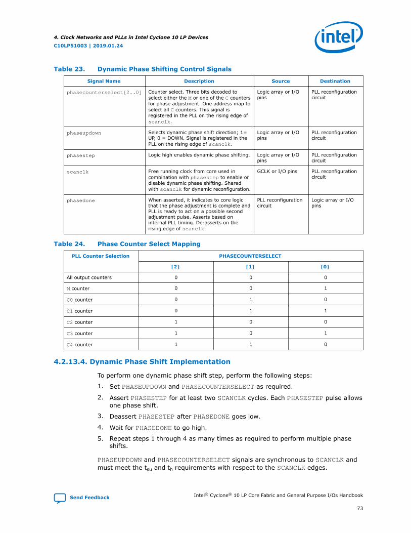
Table 23. Dynamic Phase Shifting Control Signals
Signal Name Description Source Destination
phasecounterselect[2..0] Counter select. Three bits decoded toselect either the M or one of the C countersfor phase adjustment. One address map toselect all C counters. This signal isregistered in the PLL on the rising edge ofscanclk.
Logic array or I/Opins
PLL reconfigurationcircuit
phaseupdown Selects dynamic phase shift direction; 1=UP, 0 = DOWN. Signal is registered in thePLL on the rising edge of scanclk.
Logic array or I/Opins
PLL reconfigurationcircuit
phasestep Logic high enables dynamic phase shifting. Logic array or I/Opins
PLL reconfigurationcircuit
scanclk Free running clock from core used incombination with phasestep to enable ordisable dynamic phase shifting. Sharedwith scanclk for dynamic reconfiguration.
GCLK or I/O pins PLL reconfigurationcircuit
phasedone When asserted, it indicates to core logicthat the phase adjustment is complete andPLL is ready to act on a possible secondadjustment pulse. Asserts based oninternal PLL timing. De-asserts on therising edge of scanclk.
PLL reconfigurationcircuit
Logic array or I/Opins
Table 24. Phase Counter Select Mapping
PLL Counter Selection PHASECOUNTERSELECT
[2] [1] [0]
All output counters 0 0 0
M counter 0 0 1
C0 counter 0 1 0
C1 counter 0 1 1
C2 counter 1 0 0
C3 counter 1 0 1
C4 counter 1 1 0
4.2.13.4. Dynamic Phase Shift Implementation
To perform one dynamic phase shift step, perform the following steps:
1. Set PHASEUPDOWN and PHASECOUNTERSELECT as required.
2. Assert PHASESTEP for at least two SCANCLK cycles. Each PHASESTEP pulse allowsone phase shift.
3. Deassert PHASESTEP after PHASEDONE goes low.
4. Wait for PHASEDONE to go high.
5. Repeat steps 1 through 4 as many times as required to perform multiple phaseshifts.
PHASEUPDOWN and PHASECOUNTERSELECT signals are synchronous to SCANCLK andmust meet the tsu and th requirements with respect to the SCANCLK edges.
4. Clock Networks and PLLs in Intel Cyclone 10 LP Devices
C10LP51003 | 2019.01.24
Send Feedback Intel® Cyclone® 10 LP Core Fabric and General Purpose I/Os Handbook
73

You can repeat dynamic phase-shifting indefinitely. For example, in a design where theVCO frequency is set to 1,000 MHz and the output clock frequency is set to 100 MHz,performing 40 dynamic phase shifts (each one yields 125 ps phase shift) results inshifting the output clock by 180º, which is a phase shift of 5 ns.
Figure 60. Dynamic Phase Shift Timing Diagram
PHASEDONE goes low synchronous with SCANCLK
SCANCLK
PHASESTEP
PHASEUPDOWN
PHASECOUNTERSELECT
PHASEDONE
a b c d
The PHASESTEP signal is latched on the negative edge of SCANCLK (a,c) and mustremain asserted for at least two SCANCLK cycles. Deassert PHASESTEP afterPHASEDONE goes low.
On the second SCANCLK rising edge (b,d) after PHASESTEP is latched, the values ofPHASEUPDOWN and PHASECOUNTERSELECT are latched. The PLL starts dynamicphase-shifting for the specified counters and in the indicated direction.
The PHASEDONE signal is deasserted synchronous to SCANCLK at the second risingedge (b,d) and remains low until the PLL finishes dynamic phase-shifting. Dependingon the VCO and SCANCLK frequencies, PHASEDONE low time may be greater than orless than one SCANCLK cycle.
You can perform another dynamic phase-shift after the PHASEDONE signal goes fromlow to high. Each PHASESTEP pulse enables one phase shift. The PHASESTEP pulsesmust be at least one SCANCLK cycle apart.
Related Information
Phase-Locked Loop Reconfiguration (ALTPLL_RECONFIG) IP Core User GuideProvides more information about the ALTPLL_RECONFIG parameter editor.
4.2.14. Spread-Spectrum Clocking
Intel Cyclone 10 LP devices can accept a spread-spectrum input with typicalmodulation frequencies. However, the device cannot automatically detect that theinput is a spread-spectrum signal. Instead, the input signal looks like deterministicjitter at the input of the PLL. The Intel Cyclone 10 LP PLLs can track a spread-spectrum input clock as long as it is in the input jitter tolerance specifications and themodulation frequency of the input clock is below the PLL bandwidth, that is specifiedin the fitter report. Intel Cyclone 10 LP devices cannot generate spread-spectrumsignals internally.
4. Clock Networks and PLLs in Intel Cyclone 10 LP Devices
C10LP51003 | 2019.01.24
Intel® Cyclone® 10 LP Core Fabric and General Purpose I/Os Handbook Send Feedback
74

4.3. Clock Networks and PLLs in Intel Cyclone 10 LP DevicesRevision History
DocumentVersion
Changes
2018.10.22 • Updated the Example of Automatic Switchover After Loss of Clock Detection diagram.
2018.05.07 • Removed the note to the CLK[n] pin in the Clock Control Block diagram. The CLK0 pin is availablein the Intel Cyclone 10 LP devices. Note removed: CLK[n] is not available on the left side of theIntel Cyclone 10 LP devices.
• Updated the clock pin to CLK[3..0] on the left side of the Intel Cyclone 10 LP devices in the ClockNetworks and Clock Control Block Locations in Intel Cyclone 10 LP Devices diagram.
Date Version Changes
December 2017 2017.12.22 • Updated the dedicated clock pins in the Clock Networks section.• Added GCLK resources for CLK0/DIFFCLK_0p and CLK1/DIFFCLK_0n
in the Intel Cyclone 10 LP Clock Sources Connectivity to the GCLKNetworks table.
May 2017 2017.05.08 Initial release.
4. Clock Networks and PLLs in Intel Cyclone 10 LP Devices
C10LP51003 | 2019.01.24
Send Feedback Intel® Cyclone® 10 LP Core Fabric and General Purpose I/Os Handbook
75

5. I/O and High Speed I/O in Intel Cyclone 10 LP DevicesIntel Cyclone 10 LP devices offer highly configurable GPIOs with these features:
• Support for various single-ended and differential I/O standards.
• Programmable current strength, bus hold, pull-up resistors, and delays.
• Programmable slew rate control to optimize signal integrity.
• Optional open-drain output for each I/O pin.
• True and emulated LVDS buffers with LVDS SERDES implemented using logicelements in the device core.
• Programmable pre-emphasis for the true LVDS output buffers.
• Calibrated on-chip series termination (RS OCT) or driver impedance matching (RS)for single-endd I/O standards.
• Support for hot socketing implementation.
Related Information
• Intel Cyclone 10 LP Device Pin-Outs
• Intel Cyclone 10 LP Pin Connection Guidelines
5.1. Intel Cyclone 10 LP I/O Standards Support
Intel Cyclone 10 LP devices support a wide range of I/O standards, including single-ended, voltage-referenced single-ended, and differential I/O standards.
Table 25. Supported I/O Standards in Intel Cyclone 10 LP Devices
I/O Standard Type I/O Bank Direction Application StandardSupport
Input Output
3.3 V LVTTL/3.3 VLVCMOS(15)
Single-ended All Yes Yes General purpose JESD8-B
3.0 V LVTTL/3.0 VLVCMOS(15)
Single-ended All Yes Yes General purpose JESD8-B
2.5 V LVTTL/2.5 VLVCMOS
Single-ended All Yes Yes General purpose JESD8-5
1.8 V LVTTL/1.8 VLVCMOS
Single-ended All Yes Yes General purpose JESD8-7
1.5 V LVCMOS Single-ended All Yes Yes General purpose JESD8-11
1.2 V LVCMOS Single-ended All Yes Yes General purpose JESD8-12
continued...
(15) You must enable the PCI clamp diode.
C10LP51003 | 2019.01.24
Send Feedback
Intel Corporation. All rights reserved. Intel, the Intel logo, Altera, Arria, Cyclone, Enpirion, MAX, Nios, Quartusand Stratix words and logos are trademarks of Intel Corporation or its subsidiaries in the U.S. and/or othercountries. Intel warrants performance of its FPGA and semiconductor products to current specifications inaccordance with Intel's standard warranty, but reserves the right to make changes to any products and servicesat any time without notice. Intel assumes no responsibility or liability arising out of the application or use of anyinformation, product, or service described herein except as expressly agreed to in writing by Intel. Intelcustomers are advised to obtain the latest version of device specifications before relying on any publishedinformation and before placing orders for products or services.*Other names and brands may be claimed as the property of others.
ISO9001:2015Registered

I/O Standard Type I/O Bank Direction Application StandardSupport
Input Output
3.0 V PCI/3.0 V PCI-X Single-ended All Yes Yes General purpose PCI Rev. 2.2
SSTL-2 Class I and II (16) Voltage-referenced
All Yes Yes General purpose JESD8-9B
SSTL-18 Class I and II (16) Voltage-referenced
All Yes Yes General purpose JESD8-15
1.8 V HSTL Class I andII (16)
Voltage-referenced
All Yes Yes General purpose JESD8-6
1.5 V HSTL Class I andII (16)
Voltage-referenced
All Yes Yes General purpose JESD8-6
1.2 V HSTL Class I Voltage-referenced
All Yes Yes General purpose JESD8-16A
1.2 V HSTL Class II Voltage-referenced
1, 2, 5, 6 Yes —
3, 4, 7, 8 Yes Yes
Differential SSTL-2 Class Iand II (16)
Differential All Yes(17) Yes(18) General purpose JESD8-9B
Differential SSTL-18 ClassI (16)
Differential All Yes(17) Yes(18) General purpose JESD8-15
Differential SSTL-18 ClassII (16)
Differential All Yes(17) —
Differential 1.8 V HSTLClass I (16)
Differential All Yes(17) Yes(18) General purpose JESD8-6
Differential 1.8 V HSTLClass II (16)
Differential All Yes(17) —
Differential 1.5 V HSTLClass I (16)
Differential All Yes(17) Yes(18) General purpose JESD8-6
Differential 1.5 V HSTLClass II (16)
Differential All Yes(17) —
Differential 1.2 V HSTLClass I
Differential All Yes(17) Yes(18) General purpose JESD8-16A
Differential 1.2 V HSTLClass II
Differential All Yes(17) —
LVDS (dedicated) Differential 1, 2, 5, 6 Yes Yes — ANSI/TIA/EIA-644
LVDS (emulated)(19) Differential 3, 4, 5, 6,7, 8
Yes Yes — ANSI/TIA/EIA-644
continued...
(16) Even though the Intel Cyclone 10 LP I/O buffers support various I/O standards for memoryapplication, Intel does not validate nor support any IP that is intended for memory applicationssuch as DDR or DDR2.
(17) The inputs treat differential inputs as two single-ended inputs but decode only one of them.
(18) The outputs uses two single-ended outputs with the second output programmed as inverteed.
(19) Emulated LVDS, mini-LVDS, RSDS, and PPDS I/O standards requires external resistors.
5. I/O and High Speed I/O in Intel Cyclone 10 LP Devices
C10LP51003 | 2019.01.24
Send Feedback Intel® Cyclone® 10 LP Core Fabric and General Purpose I/Os Handbook
77

I/O Standard Type I/O Bank Direction Application StandardSupport
Input Output
Mini-LVDS (dedicated) Differential 1, 2, 5, 6 — Yes — —
Mini-LVDS (emulated)(19) Differential 3, 4, 5, 6,7, 8
— Yes — —
RSDS (dedicated) Differential 1, 2, 5, 6 — Yes — —
RSDS (emulated)(19) Differential 3, 4, 5, 6,7, 8
— Yes — —
PPDS (dedicated) Differential 1, 2, 5, 6 — Yes — —
PPDS (emulated)(19) Differential All — Yes — —
Differential LVPECL Differential All Yes — — —
Bus LVDS Differential All Yes(20) Yes(18) — —
Related Information
• Intel Cyclone 10 LP I/O Banks Locations on page 86Shows the location of the row and column I/O banks.
• Differential I/O Standards Support on page 100
• Intel Cyclone 10 LP Device Pin-Outs
5.1.1. Intel Cyclone 10 LP I/O Standards Voltage and Pin Support
Table 26. Intel Cyclone 10 LP I/O Standards Voltage Levels and Pin Support
Note: The I/O standards that each pin type supports depends on the I/O standards that the pin'sI/O bank supports. For example, only the I/O banks 1, 2, 4, and 6 support the LVDS(dedicated) I/O standard. To determine the pin's I/O bank locations for your device, checkyour device's pin out file.
I/O Standard VCCIO (V) Pin Type Support
Input Output PLL_CLKOUT CLK User I/O
3.3 V LVTTL/3.3 V LVCMOS(21) 3.3/3.0/2.5 3.3 Yes Yes Yes
3.0 V LVTTL/3.0 V LVCMOS(21) 3.3/3.0/2.5 3.0 Yes Yes Yes
2.5 V LVTTL/2.5 V LVCMOS 3.3/3.0/2.5 2.5 Yes Yes Yes
1.8 V LVTTL/1.8 V LVCMOS 1.8/1.5 1.8 Yes Yes Yes
1.5 V LVCMOS 1.8/1.5 1.5 Yes Yes Yes
1.2 V LVCMOS 1.2 1.2 Yes Yes Yes
3.0 V PCI/3.0 V PCI-X(22) 3.0 3.0 Yes Yes Yes
continued...
(20) The inputs use LVDS input buffers.
(21) You must enable the PCI clamp diode.
(22) The 3.0 V PCI and PCI-X support is fully compatible for direct interface with 3.3 V PCI systemswithout additional components requirement. The outputs conforms to the VIH and VILrequirements of 3.3 V PCI and PCI-X inputs with sufficient noise margin.
5. I/O and High Speed I/O in Intel Cyclone 10 LP Devices
C10LP51003 | 2019.01.24
Intel® Cyclone® 10 LP Core Fabric and General Purpose I/Os Handbook Send Feedback
78

I/O Standard VCCIO (V) Pin Type Support
Input Output PLL_CLKOUT CLK User I/O
SSTL-2 Class I and II 2.5 2.5 Yes Yes Yes
SSTL-18 Class I and II 1.8 1.8 Yes Yes Yes
1.8 V HSTL Class I and II 1.8 1.8 Yes Yes Yes
1.5 V HSTL Class I and II 1.5 1.5 Yes Yes Yes
1.2 V HSTL Class I 1.2 1.2 Yes Yes Yes
1.2 V HSTL Class II 1.2 — — Yes Yes
— 1.2 Yes Yes(23) Yes(23)
Differential SSTL-2 Class I and II 2.5 — — Yes —
— 2.5 Yes — —
Differential SSTL-18 Class I 1.8 — — Yes —
— 1.8 Yes — —
Differential SSTL-18 Class II 1.8 — — Yes —
Differential 1.8 V HSTL Class I 1.8 — — Yes —
— 1.8 Yes — —
Differential 1.8 V HSTL Class II 1.8 — — Yes —
Differential 1.5 V HSTL Class I 1.5 — — Yes —
— 1.5 Yes — —
Differential 1.5 V HSTL Class II 1.5 — — Yes —
Differential 1.2 V HSTL Class I 1.2 — — Yes —
— 1.2 Yes — —
Differential 1.2 V HSTL Class II 1.2 — — Yes —
LVDS (dedicated) 2.5 2.5 — Yes(24) Yes(24)
LVDS (emulated)(25) 2.5 2.5 Yes Yes(26) Yes(26)
Mini-LVDS (dedicated) — 2.5 — — Yes(24)
Mini-LVDS (emulated)(25) — 2.5 Yes — Yes(26)
RSDS (dedicated) — 2.5 — — Yes(24)
RSDS (emulated)(25) — 2.5 Yes — Yes(26)
PPDS (dedicated) — 2.5 Yes — Yes(24)
continued...
(23) Only for I/O banks 3, 4, 7, and 8.
(24) Only for I/O banks 1, 2, 5, and 6.
(25) Emulated LVDS, mini-LVDS, RSDS, and PPDS I/O standards requires external resistors.
(26) Only for I/O banks 3, 4, 5, 6, 7, and 8.
5. I/O and High Speed I/O in Intel Cyclone 10 LP Devices
C10LP51003 | 2019.01.24
Send Feedback Intel® Cyclone® 10 LP Core Fabric and General Purpose I/Os Handbook
79
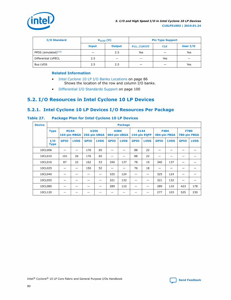
I/O Standard VCCIO (V) Pin Type Support
Input Output PLL_CLKOUT CLK User I/O
PPDS (emulated)(25) — 2.5 Yes — Yes
Differential LVPECL 2.5 — — Yes —
Bus LVDS 2.5 2.5 — — Yes
Related Information
• Intel Cyclone 10 LP I/O Banks Locations on page 86Shows the location of the row and column I/O banks.
• Differential I/O Standards Support on page 100
5.2. I/O Resources in Intel Cyclone 10 LP Devices
5.2.1. Intel Cyclone 10 LP Devices I/O Resources Per Package
Table 27. Package Plan for Intel Cyclone 10 LP Devices
Device Package
Type M164164-pin MBGA
U256256-pin UBGA
U484484-pin UBGA
E144144-pin EQFP
F484484-pin FBGA
F780780-pin FBGA
I/OType
GPIO LVDS GPIO LVDS GPIO LVDS GPIO LVDS GPIO LVDS GPIO LVDS
10CL006 — — 176 65 — — 88 22 — — — —
10CL010 101 26 176 65 — — 88 22 — — — —
10CL016 87 22 162 53 340 137 78 19 340 137 — —
10CL025 — — 150 52 — — 76 18 — — — —
10CL040 — — — — 325 124 — — 325 124 — —
10CL055 — — — — 321 132 — — 321 132 — —
10CL080 — — — — 289 110 — — 289 110 423 178
10CL120 — — — — — — — — 277 103 525 230
5. I/O and High Speed I/O in Intel Cyclone 10 LP Devices
C10LP51003 | 2019.01.24
Intel® Cyclone® 10 LP Core Fabric and General Purpose I/Os Handbook Send Feedback
80

5.2.2. Intel Cyclone 10 LP I/O Vertical Migration
Figure 61. Migration Capability Across Intel Cyclone 10 LP Devices• The arrows indicate the migration paths. The devices included in each vertical migration path are shaded.
Devices with lesser I/O resources in the same path have lighter shades.
• To achieve full I/O migration across devices in the same migration path, restrict I/O usage to match thedevice with the lowest I/O count.
DevicePackage
M164 U256 U484 E144 F484 F780
10CL006
10CL010
10CL016
10CL025
10CL040
10CL055
10CL080
10CL120
Note: To verify the pin migration compatibility, use the Pin Migration View window in theIntel Quartus Prime software Pin Planner.
5.2.3. Intel Cyclone 10 LP VREF Pins Per I/O Bank
Table 28. Number of VREF Pins Per I/O Bank in Intel Cyclone 10 LP Device Packages
Device Package I/O Bank
1 2 3 4 5 6 7 8
10CL006 U256 1 1 1 1 1 1 1 1
E144 1 1 1 1 1 1 1 1
10CL010 M164 1 1 1 1 1 1 1 1
U256 1 1 1 1 1 1 1 1
E144 1 1 1 1 1 1 1 1
10CL016 M164 2 2 2 2 2 2 2 2
U256 2 2 2 2 2 2 2 2
U484 2 2 2 2 2 2 2 2
E144 2 2 2 2 2 2 2 2
F484 2 2 2 2 2 2 2 2
10CL025 U256 1 1 1 1 1 1 1 1
E144 1 1 1 1 1 1 1 1
10CL040 U484 4 4 4 4 4 4 4 4
F484 4 4 4 4 4 4 4 4
continued...
5. I/O and High Speed I/O in Intel Cyclone 10 LP Devices
C10LP51003 | 2019.01.24
Send Feedback Intel® Cyclone® 10 LP Core Fabric and General Purpose I/Os Handbook
81

Device Package I/O Bank
1 2 3 4 5 6 7 8
10CL055 U484 2 2 2 2 2 2 2 2
F484 2 2 2 2 2 2 2 2
10CL080 U484 3 3 3 3 3 3 3 3
F484 3 3 3 3 3 3 3 3
F780 3 3 3 3 3 3 3 3
10CL120 F484 3 3 3 3 3 3 3 3
F780 3 3 3 3 3 3 3 3
5.2.4. Intel Cyclone 10 LP LVDS Channels Support
The LVDS channels available vary among Intel Cyclone 10 LP device packages.
Table 29. LVDS Buffers in Intel Cyclone 10 LP Devices• True LVDS input is supported on top, right, and bottom I/O banks while output is supported on the right
and left I/O banks.
• Emulated LVDS input and output supported on all I/O banks.
Product Line Package LVDS Pairs Device Side LVDS Pairs Per Side
10CL006 U256 65 Top 20
Right 12
Left 11
Bottom 22
E144 22 Top 6
Right 6
Left 3
Bottom 7
10CL010 M164 26 Top 9
Right 7
Left 3
Bottom 7
U256 65 Top 20
Right 12
Left 11
Bottom 22
E144 22 Top 6
Right 6
Left 3
Bottom 7
continued...
5. I/O and High Speed I/O in Intel Cyclone 10 LP Devices
C10LP51003 | 2019.01.24
Intel® Cyclone® 10 LP Core Fabric and General Purpose I/Os Handbook Send Feedback
82

Product Line Package LVDS Pairs Device Side LVDS Pairs Per Side
10CL016 M164 22 Top 7
Right 6
Left 3
Bottom 6
U256 53 Top 14
Right 12
Left 9
Bottom 18
U484 137 Top 36
Right 37
Left 31
Bottom 33
E144 19 Top 6
Right 5
Left 2
Bottom 6
F484 137 Top 36
Right 37
Left 31
Bottom 33
10CL025 U256 52 Top 17
Right 10
Left 10
Bottom 15
E144 18 Top 5
Right 5
Left 3
Bottom 5
10CL040 U484 124 Top 33
Right 32
Left 29
Bottom 30
F484 124 Top 33
Right 32
Left 29
Bottom 30
continued...
5. I/O and High Speed I/O in Intel Cyclone 10 LP Devices
C10LP51003 | 2019.01.24
Send Feedback Intel® Cyclone® 10 LP Core Fabric and General Purpose I/Os Handbook
83

Product Line Package LVDS Pairs Device Side LVDS Pairs Per Side
10CL055 U484 132 Top 36
Right 34
Left 29
Bottom 33
F484 132 Top 36
Right 34
Left 29
Bottom 33
10CL080 U484 110 Top 29
Right 29
Left 26
Bottom 26
F484 110 Top 29
Right 29
Left 26
Bottom 26
F780 178 Top 51
Right 43
Left 35
Bottom 49
10CL120 F484 103 Top 28
Right 26
Left 25
Bottom 24
F780 230 Top 65
Right 53
Left 49
Bottom 63
5.3. Intel FPGA I/O IP Cores for Intel Cyclone 10 LP Devices
The I/O system is supported by several Intel FPGA I/O IP cores.
• ALTIOBUF—supports operations of the GPIO components.
• ALTLVDS—supports operations of the high-speed source-synchronous SERDES.
• ALTDDIO—supports configuration and implementation of double data rate I/Oregisters.
5. I/O and High Speed I/O in Intel Cyclone 10 LP Devices
C10LP51003 | 2019.01.24
Intel® Cyclone® 10 LP Core Fabric and General Purpose I/Os Handbook Send Feedback
84

Related Information
• LVDS SERDES Transmitter/Receiver IP Cores User Guide
• I/O Buffer (ALTIOBUF) IP Core User Guide
• Double Data Rate I/O (ALTDDIO_IN, ALTDDIO_OUT, and ALTDDIO_BIDIR) IPCores User Guide
5.4. Intel Cyclone 10 LP I/O Elements
The Intel Cyclone 10 LP I/O elements (IOEs) contain a bidirectional I/O buffer and fiveregisters for registering input, output, output-enable signals, and complete embeddedbidirectional single data rate (SDR) and double data rate (DDR) transfer.
Note: Intel does not validate or support any IP that is intended for memory application, suchas DDR, in Intel Cyclone 10 LP devices.
Each IOE contains one input register, two output registers, and two output-enable(OE) registers:
• The two output registers and two OE registers are used for DDR applications.
• You can use the input registers for fast setup times and output registers for fastclock-to-output times.
• You can use the OE registers for fast clock-to-output enable times.
You can use the IOEs for input, output, or bidirectional data paths. The I/O pinssupport various single-ended and differential I/O standards.
5. I/O and High Speed I/O in Intel Cyclone 10 LP Devices
C10LP51003 | 2019.01.24
Send Feedback Intel® Cyclone® 10 LP Core Fabric and General Purpose I/Os Handbook
85

Figure 62. IOE Structure in Bidirectional Configuration for SDR Mode
D Q
ENA
D Q
ENA
VCCIO
VCCIO
Optional PCI Clamp
ProgrammablePull-UpResistor
Bus HoldInput Pin toInput Register
Delayor Input Pin to
Logic Array Delay
OutputPin Delay
clkin
oe_in
data_in0
data_in1
sclr/preset
Chip-Wide Reset
aclr/prn
oe_out
clkout
OE
OE Register
Current Strength ControlOpen-Drain Out
Columnor Row
Interconnect
io_clk[5..0]
Slew Rate Control
ACLR/PRN
ACLR/PRN
Output Register
D Q
ENA
ACLR/PRN
Input Register
Tri-state control is not available for outputsconfigured with true differential I/O standards
5.4.1. Intel Cyclone 10 LP I/O Banks Architecture
The device I/O pins are grouped into eight groups and each group is associataed withan I/O bank. Every I/O bank in the device has a separate power bus.
The only exception is HSTL-12 Class II, which is only supported in column I/O banks.
There are two types of I/O banks in Intel Cyclone 10 LP devices:
• Row I/O banks—I/O banks 1, 2, 5, and 6, located on the left and right side of thedevice
• Column I/O banks—I/O banks 3, 4, 7, and 8, located on the top and bottom sideof the device
Only the column I/O banks support the 1.2 V HSTL Class II I/O standard. Both rowand column I/O banks support all the other single-ended and differential I/Ostandards that the Intel Cyclone 10 LP device supports.
5.4.2. Intel Cyclone 10 LP I/O Banks Locations
The I/O banks are located at the periphery of the device.
5. I/O and High Speed I/O in Intel Cyclone 10 LP Devices
C10LP51003 | 2019.01.24
Intel® Cyclone® 10 LP Core Fabric and General Purpose I/Os Handbook Send Feedback
86

Figure 63. I/O Banks for Intel Cyclone 10 LP DevicesThis figure is only a graphical representation showing the topc view of the silicon die.
2
1
5
6
3 4
8 7
Row I/O bank
Column I/O bank
OCT Calibration block
OCT calibration block coverage
For details about the I/O banks and the exact pin locations in each device package,refer to the Intel Quartus Prime software and the relevant device pin-out file.
Related Information
• Intel Cyclone 10 LP I/O Standards Voltage and Pin Support on page 78Lists the supported I/O direction, voltages, and pin type for each I/O standard.
• Intel Cyclone 10 LP I/O Standards Support on page 76Lists the supported I/O standards and availability of each I/O standard in thedevice I/O banks.
• Intel Cyclone 10 LP Device Pin-Outs
• OCT Calibration on page 97
5.5. Intel Cyclone 10 LP Clock Pins Input Support
Intel Cyclone 10 LP clock pins have multiple purposes.
Table 30. Clock Pins Input Support in Intel Cyclone 10 LP Devices
Clock Pin Input Support
CLK Input support for single-ended and voltage-referenced standards.
DIFFCLK Input support for differential I/O standards. If used as DIFFCLK pins:• You can use DC or AC coupling depending on the interface requirements.• The input requires external termination.
5. I/O and High Speed I/O in Intel Cyclone 10 LP Devices
C10LP51003 | 2019.01.24
Send Feedback Intel® Cyclone® 10 LP Core Fabric and General Purpose I/Os Handbook
87

Related Information
• Intel Cyclone 10 LP I/O Standards Support on page 76
• Intel Cyclone 10 LP I/O Standards Voltage and Pin Support on page 78
• Differential I/O Standards Support on page 100
5.6. Programmable IOE Features in Intel Cyclone 10 LP Devices
The Intel Cyclone 10 LP I/O buffers support a range of programmable features. Thesefeatures increase the flexibility of I/O utilization and provide an alternative to reducethe usage of external discrete components such as a pull-up resistor and a diode.
Table 31. Summary of Supported Intel Cyclone 10 LP Programmable I/O BufferFeatures and Settings
Feature Setting Condition Assignment Name
Open Drain • On• Off—Default
To enable this feature,use the OPNDRNprimitive.
—
Bus-Hold • On• Off—Default
Disabled if you use theweak pull-up resistorfeature.
Enable Bus-Hold Circuitry
Pull-up Resistor • On• Off—Default
Disabled if you use thebus-hold feature.
Weak Pull-Up Resistor
Slew Rate Control • 0 (Slow)• 1 (Medium)• 2 (Fast)—Default
Disabled if you use OCTwith calibration.
Slew Rate
PCI Clamp Diode • On—Default for input pins usingsupported I/O standards
• Off—Default for output pinsexcept 3.0 V PCI/PCI-X.
— PCI I/O
Pre-Emphasis 0 (disabled), 1 (enabled). Default is1.
— Programmable Pre-emphasis
5.6.1. Programmable Open Drain
The optional open-drain output for each I/O pin is equivalent to an open collectoroutput. If it is configured as an open drain, the logic value of the output is either high-Z or logic low.
Use an external resistor to pull the signal to a logic high.
5.6.2. Programmable Bus Hold
Each I/O pin provides an optional bus-hold feature that is active only afterconfiguration. When the device enters user mode, the bus-hold circuit captures thevalue that is present on the pin by the end of the configuration.
The bus-hold circuitry holds the signal on an I/O pin at its last-driven state until thenext input signal is present. Because of this, you do not require an external pull-up orpull-down resistor to hold a signal level when the bus is tri-stated.
5. I/O and High Speed I/O in Intel Cyclone 10 LP Devices
C10LP51003 | 2019.01.24
Intel® Cyclone® 10 LP Core Fabric and General Purpose I/Os Handbook Send Feedback
88

For each I/O pin, you can individually specify that the bus-hold circuitry pulls non-driven pins away from the input threshold voltage—where noise can cause unintendedhigh-frequency switching. To prevent over-driving signals, the bus-hold circuitry drivesthe voltage level of the I/O pin lower than the VCCIO level.
If you enable the bus-hold feature, you cannot use the programmable pull-up option.To configure the I/O pin for differential signals, disable the bus-hold feature.
The bus-hold circuitry is not available on dedicated clock pins.
For the specific sustaining current for each VCCIO voltage level driven through theresistor and for the overdrive current used to identify the next driven input level, referto the device datasheet.
Related Information
Intel Cyclone 10 LP Device Datasheet
5.6.3. Programmable Pull-Up Resistor
Each I/O pin provides an optional programmable pull-up resistor during user mode.The pull-up resistor weakly holds the I/O to the VCCIO level.
The Intel Cyclone 10 LP device supports programmable weak pull-up resistors only onuser I/O pins but not on dedicated configuration pins, dedicated clock pins, or JTAGpins .
If you enable the weak pull-up resistor, you cannot use the bus-hold feature.
Note: When the optional DEV_OE signal drives low, all I/O pins remain tri-stated even if theprogrammable pull-up option is enabled.
5.6.4. Programmable Current Strength
You can use the programmable current strength to mitigate the effects of high signalattenuation that is caused by a long transmission line or a legacy backplane.
Table 32. Programmable Current Strength Settings for Intel Cyclone 10 LP DevicesThe output buffer for each Intel Cyclone 10 LP device I/O pin has a programmable current strength control forthe I/O standards listed in this table.
I/O Standard IOH / IOL Current Strength Setting (mA)(Default setting in bold)
Column I/O Row I/O
3.3 V LVCMOS 2
3.3 V LVTTL 8, 4
3.0 V LVTTL/3.0 V LVCMOS 16, 12, 8, 4
2.5 V LVTTL/2.5 V LVCMOS 16, 12, 8, 4
1.8 V LVTTL/1.8 V LVCMOS 16, 12, 10, 8, 6, 4, 2
1.5 V LVCMOS 16, 12, 10, 8, 6, 4, 2
1.2 V LVCMOS 12, 10, 8, 6, 4, 2 10, 8, 6, 4, 2
SSTL-2 Class I 12, 8continued...
5. I/O and High Speed I/O in Intel Cyclone 10 LP Devices
C10LP51003 | 2019.01.24
Send Feedback Intel® Cyclone® 10 LP Core Fabric and General Purpose I/Os Handbook
89

I/O Standard IOH / IOL Current Strength Setting (mA)(Default setting in bold)
Column I/O Row I/O
SSTL-2 Class II 16
SSTL-18 Class I 12, 10, 8
SSTL-18 Class II 16, 12
1.8 V HSTL Class I 12, 10, 8
1.8 V HSTL Class II 16
1.5 V HSTL Class I 12, 10, 8
1.5 V HSTL Class II 16
1.2 V HSTL Class I 12, 10, 8 10, 8
1.2 V HSTL Class II 14 —
Differential SSTL-2 Class I 12, 8
Differential SSTL-2 Class II 16
Differential SSTL-18 Class I 12, 10, 8—
Differential SSTL-18 Class II 12. 16
Differential 1.8 V HSTL Class I 12, 10, 8
Differential 1.8 V HSTL Class II 16
Differential 1.5 V HSTL Class I 12, 10, 8
Differential 1.5 V HSTL Class II 16
Differential 1.2 V HSTL Class I 12, 10, 8
Differential 1.2 V HSTL Class II 14
BLVDS 16, 12, 8
Default current strength setting in the Intel Quartus Prime software:
• All non-voltage referenced I/O standards—50–Ω OCT without calibration
• SSTL Class I and HSTL Class I I/O standards—50–Ω OCT without calibration
• SSTL Class II and HSTL Class II I/O standards—25–Ω OCT without calibration
Programmable current strength is not available if you use RS OCT.
Note: Intel recommends that you perform IBIS or SPICE simulations to determine the bestcurrent strength setting for your specific application.
5.6.5. Programmable Output Slew Rate Control
You have the option of three settings for programmable slew rate control—0, 1, and 2with 2 as the default setting. Setting 0 is the slow slew rate and 2 is the fast slew rate.
• Fast slew rate—provides high-speed transitions for high-performance systems.
• Slow slew rate—reduces system noise and crosstalk but adds a nominal delay tothe rising and falling edges.
5. I/O and High Speed I/O in Intel Cyclone 10 LP Devices
C10LP51003 | 2019.01.24
Intel® Cyclone® 10 LP Core Fabric and General Purpose I/Os Handbook Send Feedback
90

Table 33. Programmable Output Slew Rate Control for Intel Cyclone 10 LP DevicesThis table lists the I/O standards and current strength settings that support programmable output slew ratecontrol. For I/O standards and current strength settings that do not support programmable slew rate control,the default slew rate setting is 2 (fast slew rate).
I/O Standard IOH / IOL Current Strength Supporting Slew RateControl
3.0 V LVTTL/3.0 V LVCMOS 16, 12, 8
2.5 V LVTTL/2.5 V LVCMOS 16, 12, 8
1.8 V LVTTL/1.8 V LVCMOS 16, 12, 10, 8
1.5 V LVCMOS 16, 12, 10, 8
1.2 V LVCMOS 12, 10, 8
SSTL-2 Class I 12, 8
SSTL-2 Class II 16
SSTL-18 Class I 12, 10, 8
SSTL-18 Class II 16, 12
1.8 V HSTL Class I 12, 10, 8
1.8 V HSTL Class II 16
1.5 V HSTL Class I 12, 10, 8
1.5 V HSTL Class II 16
1.2 V HSTL Class I 12, 10, 8
1.2 V HSTL Class II 14
Differential SSTL-2 Class I 12, 8
Differential SSTL-2 Class II 16
Differential SSTL-18 12, 10, 8
Differential 1.8 V HSTL 12, 10, 8
Differential 1.5 V HSTL 12, 10, 8
Differential 1.2 V HSTL 12, 10, 8
BLVDS 16, 12, 8
You can specify the slew rate on a pin-by-pin basis because each I/O pin contains aslew rate control. The slew rate control affects both the rising and falling edges.
Note: Intel recommends that you perform IBIS or SPICE simulations to determine the bestslew rate setting for your specific application.
5.6.6. Programmable IOE Delay
You can activate the programmable IOE delays to ensure zero hold times, minimizesetup times, increase clock-to-output times, or delay the clock input signal. Thisfeature helps read and write timing margins because it minimizes the uncertaintiesbetween signals in the bus.
Each pin can have a different delay value to ensure signals within a bus have the samedelay going into or out of the device.
5. I/O and High Speed I/O in Intel Cyclone 10 LP Devices
C10LP51003 | 2019.01.24
Send Feedback Intel® Cyclone® 10 LP Core Fabric and General Purpose I/Os Handbook
91

Each dual-purpose clock input pin provides a programmable delay to the global clocknetworks.
Table 34. Programmable Delay Chain
Programmable Delays Intel Quartus Prime Logic Option
Input pin-to-logic array delay Input delay from pin to internal cells
Input pin-to-input register delay Input delay from pin to input register
Output pin delay Delay from output register to output pin
Dual-purpose clock input pin delay Input delay from dual-purpose clock pin to fan-out destinations
There are two paths in the IOE for an input to reach the logic array. Each of the twopaths can have a different delay. This allows you to adjust delays from the pin to theinternal logic element (LE) registers that reside in two different areas of the device.You must set the two combinational input delays with the input delay from pin tointernal cells logic option in the Intel Quartus Prime software for each path. If the pinuses the input register, one of the delays is disregarded and the delay is set with theinput delay from pin to input register logic option in the Intel Quartus Prime software.
The IOE registers in each I/O block share the same source for the preset or clearfeatures. You can program preset or clear for each individual IOE, but you cannot useboth features simultaneously. You can also program the registers to power-up high orlow after configuration is complete. If programmed to power-up low, an asynchronousclear can control the registers. If programmed to power-up high, an asynchronouspreset can control the registers. This feature prevents the inadvertent activation of theactive-low input of another device upon power up. If one register in an IOE uses apreset or clear signal, all registers in the IOE must use that same signal if they requirepreset or clear. Additionally, a synchronous reset signal is available for the IOEregisters.
Related Information
• Timing Closure and Optimization chapter, Volume 2: Design Implementation andOptimization, Intel Quartus Prime Handbook
Provides more information about the input and output pin delay settings.
• Intel Cyclone 10 LP Device Datasheet
5.6.7. PCI Clamp Diode
The Intel Cyclone 10 LP devices are equipped with optional PCI clamp diode that youcan enable for the input and output of each I/O pin. You can use this diode to protectI/O pins during voltage overshoot.
The PCI clamp diode is available and enabled by default in the Intel Quartus Primesoftware for the following I/O standards:
• 3.3 V LVTTL/3.3 V LVCMOS
• 3.0 V LVTTL/3.0 V LVCMOS
• 2.5 V LVTTL/2.5 V LVCMOS
• 3.0 V PCI/PCI-X
5. I/O and High Speed I/O in Intel Cyclone 10 LP Devices
C10LP51003 | 2019.01.24
Intel® Cyclone® 10 LP Core Fabric and General Purpose I/Os Handbook Send Feedback
92

Dual-purpose configuration pins support the diode in user mode if you do not use thepins as configuration pins for the selected configuration scheme. For example, if youuse the active serial (AS) configuration scheme, you cannot use the clamp diode onthe ASDO and nCSO pins in user mode. The dedicated configuration pins do notsupport the on-chip diode.
Note: For the 3.3 V LVTTL, 3.3 V LVCMOS, 3.0 V LVTTL, and 3.0 V LVCMOS I/O standards,you must enable the PCI clamp diode.
5.6.8. Programmable Pre-Emphasis
The differential output voltage (VOD) setting and the output impedance of the driverset the output current limit of a high-speed transmission signal. At a high frequency,the slew rate may not be fast enough to reach the full VOD level before the next edge,producing pattern-dependent jitter. Pre-emphasis momentarily boosts the outputcurrent during switching to increase the output slew rate.
Pre-emphasis increases the amplitude of the high-frequency component of the outputsignal. This increase compensates for the frequency-dependent attenuation along thetransmission line.
The overshoot introduced by the extra current occurs only during change of stateswitching. This overshoot increases the output slew rate but does not ring, unlike theovershoot caused by signal reflection. The amount of pre-emphasis required dependson the attenuation of the high-frequency component along the transmission line.
Figure 64. LVDS Output with Programmable Pre-Emphasis
OUT
OUT
V OD
V P
V P
Voltage boostfrom pre-emphasis
Differential outputvoltage (peak–peak)
Table 35. Intel Quartus Prime Software Assignment for Programmable Pre-Emphasis
Field Assignment
To tx_out
Assignment name Programmable Pre-emphasis
Allowed values 0 (disabled), 1 (enabled). Default is 1.
5.7. I/O Standards Termination
Voltage-referenced and differential I/O standards requires different terminationschemes.
5. I/O and High Speed I/O in Intel Cyclone 10 LP Devices
C10LP51003 | 2019.01.24
Send Feedback Intel® Cyclone® 10 LP Core Fabric and General Purpose I/Os Handbook
93

According to JEDEC standards, the following I/O standards do not specify arecommended termination scheme:
• 3.3-V LVTTL
• 3.0 V LVTTL/3.0 V LVCMOS
• 2.5 V LVTTL/2.5 V LVCMOS
• 1.8 V LVTTL/1.8 V LVCMOS
• 1.5 V LVCMOS
• 1.2 V LVCMOS
• 3.0 V PCI/PCI-X
5.7.1. Voltage-Referenced I/O Standards Termination
Voltage-referenced I/O standards require an input reference voltage (VREF) and atermination voltage (VTT). The reference voltage of the receiving device tracks thetermination voltage of the transmitting device.
Figure 65. HSTL I/O Standard Termination
HSTL Class I HSTL Class II
ExternalOn-Board
Termination
OCT with and withoutCalibration
VTT
50 Ω
50 Ω
VTT
50 Ω
VTT
50 Ω
Transmitter TransmitterReceiver Receiver
VTT
50 Ω
Transmitter Receiver
VTT
50 Ω
VTT
50 Ω
Transmitter Receiver
Series OCT
50 Ω
Series OCT25 Ω
VREFVREF
VREFVREF
Termination
50 Ω
50 Ω
50 Ω
Figure 66. SSTL I/O Standard Termination
SSTL Class I SSTL Class II
ExternalOn-Board
Termination
OCT withand withoutCalibration
VTT
50 Ω25 Ω
VTT
50 Ω25 Ω
VTT
50 Ω
Transmitter TransmitterReceiver Receiver
VTT
50 Ω50 Ω
Transmitter Receiver
Series OCT
50 ΩVTT
50 Ω25 Ω
50 Ω
VTT
50 Ω
Transmitter Receiver
Series OCT
VREF VREF
VREFVREF
Termination
50 Ω 50 Ω
5. I/O and High Speed I/O in Intel Cyclone 10 LP Devices
C10LP51003 | 2019.01.24
Intel® Cyclone® 10 LP Core Fabric and General Purpose I/Os Handbook Send Feedback
94

5.7.2. Differential I/O Standards Termination
Differential I/O standards typically require a termination resistor between the twosignals at the receiver. The termination resistor must match the differential loadimpedance of the bus.
Figure 67. Differential HSTL I/O Standard Termination
Transmitter Receiver
50 Ω
50 Ω
V TT
50 Ω
50 Ω
V TT
50 Ω
V TT
50 Ω
V TT
Transmitter Receiver Transmitter Receiver
Series OCT 25 Ω Series OCT 50 Ω
Transmitter Receiver
50 Ω
50 Ω
V TT
50 Ω
V TT
50 Ω
50 Ω
V TT
50 Ω
V TT
50 Ω
50 Ω
V TT
50 Ω
50 Ω
V TT
50 Ω
V TT
50 Ω
V TT
Differential HSTL Class ITermination
OCT
Differential HSTL Class II
External On-Board
Termination
50 Ω
50 Ω
Figure 68. Differential SSTL I/O Standard TerminationOnly differential SSTL-2 I/O standard supports Class II output.
Differential SSTL Class I Differential SSTL Class II
ExternalOn-Board
Termination
OCT
Transmitter Receiver
50 Ω
50 Ω 50 Ω
50 Ω
VTT VTT
25 Ω
25 Ω
Transmitter Receiver
50 Ω
50 Ω 50 Ω
50 Ω
VTT VTT
25 Ω
25 Ω
50 Ω 50 Ω
VTT VTT
Transmitter Receiver
50 Ω
50 Ω 50 Ω
50 Ω
VTT VTT
50 Ω 50 Ω
VTT VTT
Series OCT25 Ω
Transmitter Receiver
50 Ω
50 Ω 50 Ω
50 Ω
VTT VTT
50 Ω
Series OCT
Termination
Related Information
• Differential SSTL I/O Standard in Intel Cyclone 10 LP Devices on page 106
• Differential HSTL I/O Standard in Intel Cyclone 10 LP Devices on page 107
5. I/O and High Speed I/O in Intel Cyclone 10 LP Devices
C10LP51003 | 2019.01.24
Send Feedback Intel® Cyclone® 10 LP Core Fabric and General Purpose I/Os Handbook
95

5.7.3. Intel Cyclone 10 LP On-Chip I/O Termination
The on-chip termination (OCT) block in Intel Cyclone 10 LP devices provides I/Oimpedance matching and termination capabilities. OCT maintains signal quality, savesboard space, and reduces external component costs.
The devices support driver impedance matching to match the impedance of thetransmission line, which is typically 25 Ω or 50 Ω. Impedance matching uses thecapabilities of the output driver and is subject to a certain degree of variation,depending on the process, voltage, and temperature.
Table 36. OCT Schemes Supported in Intel Cyclone 10 LP Devices
Direction OCT Schemes I/O Bank Support
Output RS OCT with calibration Top, bottom, and right I/O banks
RS OCT without calibration All I/O banks
The Intel Cyclone 10 LP devices support serial (RS) OCT for single-ended output pinsand bidirectional pins.
• For bidirectional pins, OCT is active for output only.
• VCCIO and VREF must be compatible for all I/O pins to enable RS OCT in an I/Obank.
• I/O standards that support different RS values can reside in the same I/O bank iftheir VCCIO and VREF do not conflict.
• Dedicated configuration pins and JTAG pins do not support impedance matching orseries termination.
Figure 69. RS OCT with Calibration in Intel Cyclone 10 LP DevicesIn this figure, the RS is the intrinsic impedance of the transistors that make up the I/O buffer.
V CCIO
R S
R S
GND
Z 0
DriverSeries Termination
ReceivingDevice
5. I/O and High Speed I/O in Intel Cyclone 10 LP Devices
C10LP51003 | 2019.01.24
Intel® Cyclone® 10 LP Core Fabric and General Purpose I/Os Handbook Send Feedback
96

Figure 70. RS OCT without Calibration in Intel Cyclone 10 LP DevicesIn this figure, the RS is the intrinsic transistor impedance.
V CCIO
R S
R S
GND
Z 0
DriverSeries Termination
ReceivingDevice
Related Information
Intel Cyclone 10 LP Device Datasheet
5.7.3.1. OCT Calibration
The OCT calibration circuit compares the total impedance of the output buffer to theexternal resistors connected to the RUP and RDN pins. The circuit dynamically adjuststhe output buffer impedance until it matches the external resisters.
In Intel Cyclone 10 LP devices, there is one OCT calibration block on each side of thedevice. The calibration block supports both I/O banks on the side on which it islocated:
• If you enable OCT calibration for both I/O banks on the same device side, use thesame VCCIO on both banks.
• If the VCCIO values of the I/O banks on the same side are not the same, you canuse OCT calibration only on the I/O bank that contains the calibration block.
Each OCT calibration block comes with a pair of RUP and RDN pins. During calibration,the RUP and RDN pins are each connected through an external 25 Ω ±1% or50 Ω ±1% resistor for respective on-chip series termination value of 25 Ω or 50 Ω:
• RUP—connected to VCCIO.
• RDN—connected to GND.
5. I/O and High Speed I/O in Intel Cyclone 10 LP Devices
C10LP51003 | 2019.01.24
Send Feedback Intel® Cyclone® 10 LP Core Fabric and General Purpose I/Os Handbook
97

Figure 71. RS OCT with Calibration SetupThis figure shows the external calibration resistors setup on the RUP and RDN pins and the associated OCTcalibration circuitry.
Calibrated OCT with RUP and RDN pins
OCT Calibration
Circuitry
VCCIO
VCCIO
RUP
RDN
External CalibrationResistor
External CalibrationResistor
GND
The OCT calibration circuit compares the external resistors to the internal resistanceusing comparators. The OCT calibration block uses the comparators' output todynamically adjust buffer impedance.
During calibration, the resistance of the RUP and RDN pins varies. To estimate of themaximum possible current through the external calibration resistors, assume aminimum resistance of 0 Ω on the RUP and RDN pins.
The RUP and RDN pins go to a tri-state condition when calibration is completed or notrunning. These two pins are dual-purpose I/Os and function as regular I/Os if you donot use the calibration circuit.
Related Information
Intel Cyclone 10 LP I/O Banks Locations on page 86
5. I/O and High Speed I/O in Intel Cyclone 10 LP Devices
C10LP51003 | 2019.01.24
Intel® Cyclone® 10 LP Core Fabric and General Purpose I/Os Handbook Send Feedback
98

5.7.3.2. RS OCT in Intel Cyclone 10 LP Devices
Table 37. Selectable I/O Standards for RS OCT
This table lists the output termination settings for RS OCT with and without calibration on different I/Ostandards.
I/O Standard CalibratedRSOCT
(Ω)
UncalibratedRS OCT
(Ω)
Column I/O Row I/O Column I/O Row I/O
3.0 V LVTTL/3.0V LVCMOS 25, 50 25, 50
2.5 V LVTTL/2.5 V LVCMOS 25, 50 25, 50
1.8 V LVTTL/1.8 V LVCMOS 25, 50 25, 50
1.5 V LVCMOS 25, 50 25, 50
1.2 V LVCMOS 25, 50 50 25, 50 50
SSTL-2 Class I 50 50
SSTL-2 Class II 25 25
SSTL-18 Class I 50 50
SSTL-18 Class II 25 25
1.8 V HSTL Class I 50 50
1.8 V HSTL Class II 25 25
1.5 V HSTL Class I 50 50
1.5 V HSTL Class II 25 25
1.2 V HSTL Class I 50 50
1.2 V HSTL Class II 25 — 25 —
Differential SSTL-2 Class I 50 50
Differential SSTL-2 Class II 25 25
Differential SSTL-18 50 — 50 —
Differential 1.8 V HSTL 50 — 50 —
Differential 1.5 V HSTL 50 — 50 —
Differential 1.2 V HSTL 50 — 50 —
Related Information
Intel Cyclone 10 LP Device Datasheet
5.8. Intel Cyclone 10 LP High-Speed Differential I/Os and SERDES
The Intel Cyclone 10 LP devices use registers and logic in the core fabric to implementLVDS input and output interfaces.
5. I/O and High Speed I/O in Intel Cyclone 10 LP Devices
C10LP51003 | 2019.01.24
Send Feedback Intel® Cyclone® 10 LP Core Fabric and General Purpose I/Os Handbook
99

• For LVDS transmitters and receivers, Intel Cyclone 10 LP devices use the thedouble data rate I/O (DDIO) registers that reside in the I/O elements (IOE). Thisarchitecture improves performance with regards to the receiver input skew margin(RSKM) or transmitter channel-to-channel skew (TCCS).
• For the LVDS serializer/deserializer (SERDES), Intel Cyclone 10 LP devices uselogic elements (LE) registers.
• The device uses shift registers, internal phase-locked loops (PLLs), and I/O cells toperform serial-to-parallel conversions on incoming data and parallel-to-serialconversion on outgoing data.
Note: In Intel Cyclone 10 LP devices, the interface configured using the ALTLVDS IP corealways sends the MSB of your parallel data first.
Related Information
LVDS SERDES Transmitter/Receiver IP Cores User Guide
5.8.1. High-Speed Differential I/O Interface
The Intel Cyclone 10 LP devices support LVDS, RSDS, mini-LVDS, and PPDS high-speed differential I/O standards.
Differential Input
The Intel Cyclone 10 LP devices features true input buffers for these I/O standards onthe top, bottom, and right I/O banks.
Differential Output
The Intel Cyclone 10 LP devices features dedicated differential output buffers:
• The true output drivers are available on the row I/O banks.
• Some of the differential pin pairs (p and n pins) are not located on adjacent pins.In these cases, a power pin is located between the p and n pins.
The Intel Cyclone 10 LP devices provide emulated support for these I/O standards onall columns and row I/O banks:
• Emulated differential output uses a pair of single-ended output pins.
• In the pin pair, the second output pin is programmed as inverted.
• The emulated differential output requires an external resistor network.
5.8.2. Differential I/O Standards Support
Table 38. Differential I/O Standards Support in Intel Cyclone 10 LP I/O Banks
I/O Standard I/O Bank External Resistor atTransmitter
TX RX
LVDS 1, 2, 5, 6 Not required Yes Yes
All Three resistors
RSDS 1, 2, 5, 6 Not required Yes —
3, 4, 7, 8 Three resistors
continued...
5. I/O and High Speed I/O in Intel Cyclone 10 LP Devices
C10LP51003 | 2019.01.24
Intel® Cyclone® 10 LP Core Fabric and General Purpose I/Os Handbook Send Feedback
100

I/O Standard I/O Bank External Resistor atTransmitter
TX RX
All Single resistor
Mini-LVDS 1, 2, 5, 6 Not required Yes —
All Three resistors
PPDS 1, 2, 5, 6 Not required Yes —
All Three resistors
Bus LVDS All Single resistor Yes Yes
Differential LVPECL All — — Yes
Differential SSTL-2 All — Yes Yes
Differential SSTL-18 All — Yes Yes
Differential 1.8 V HSTL All — Yes Yes
Differential 1.5 V HSTL All — Yes Yes
Differential 1.2 V HSTL All — Yes Yes
The following conditions apply to the differential I/O standard support:
• The Bus LVDS transmitter and receiver fMAX depend on system topology andperformance requirement.
• The Differential LVPECL I/O standard is supported only on dedicated clock inputpins.
• The following differential I/O standards are supported only on clock input pins andPLL clock output pins:
— Differential SSTL-2 and Differential SSTL-18
— Differential 1.8 V HSTL, Differential 1.5 V HSTL, and Differential 1.2 V HSTL
• PLL clock output pins do not support Class II interface for these diffential I/Ostandards:
— Differential SSTL-18
— Differential 1.8 V HSTL, Differential 1.5 V HSTL, and Differential 1.2 V HSTL
• Differential 1.2 V HSTL Class II I/O standard is supported only in column I/Obanks.
Related Information
• Intel Cyclone 10 LP I/O Standards Voltage and Pin Support on page 78Lists the supported I/O direction, voltages, and pin type for each I/O standard.
• Intel Cyclone 10 LP I/O Standards Support on page 76Lists the supported I/O standards and availability of each I/O standard in thedevice I/O banks.
5.8.2.1. LVDS I/O Standard in Intel Cyclone 10 LP Devices
The LVDS I/O standard is a high-speed, low-voltage swing, low power, and GPIOinterface standard.
Intel Cyclone 10 LP devices meet the ANSI/TIA/EIA-644 standard with the followingexceptions:
5. I/O and High Speed I/O in Intel Cyclone 10 LP Devices
C10LP51003 | 2019.01.24
Send Feedback Intel® Cyclone® 10 LP Core Fabric and General Purpose I/Os Handbook
101

• The maximum differential output voltage (VOD) is increased to 600 mV. Themaximum VOD for ANSI specification is 450 mV.
• The input voltage range is reduced to the range of 1.0 V to 1.6 V, 0.5 V to 1.85 V,or 0 V to 1.8 V based on different frequency ranges. The ANSI/TIA/EIA-644specification supports an input voltage range of 0 V to 2.4 V.
The Intel Cyclone 10 LP left and right I/O banks (row I/Os) support true LVDStransmitters. The top and bottom I/O banks support emulated LVDS transmitters withexternal resistors.
For the LVDS receiver, you require an external 100 Ω termination resistor between thetwo signals at the input buffer.
Figure 72. LVDS Interface with True Output Buffer on the Right Side I/O BanksThis figure shows a point-to-point LVDS interface using the true LVDS output and input buffers.
Transmitting DeviceFPGA Device
100 WLogicArray 100 W
Input Buffer Output Buffer
Receiving Devicetxout +
txout -
rxin +
rxin -
txout +
txout -
rxin +
rxin -
50 Ω
50 Ω
50 Ω
50 Ω
Figure 73. LVDS Interface with External Resistor Network on the Top and Bottom I/OBanksThis figure shows a point-to-point LVDS interface using two single-ended output buffers and external resistors.In the figure, RS is 120 Ω while RP is 170 Ω.
LVDS Receiver
100 Ω 50 Ω
FPGA Device
Resistor Network
EmulatedLVDS Transmitter
RS
RP
RS
50 Ω
Related Information
Intel Cyclone 10 LP Device Datasheet
5.8.2.2. Bus LVDS I/O Standard in Intel Cyclone 10 LP Devices
The Bus LVDS I/O standard is a multipoint I/O standard that supports bidirectionalhalf-duplex communication.
The Intel Cyclone 10 LP top, bottom, and right side I/O banks support the Bus LVDSI/O standard. For the Bus LVDS transmitter, Intel Cyclone 10 LP devices use emulateddifferential output. For the Bus LVDS receiver, Intel Cyclone 10 LP devices use the true
5. I/O and High Speed I/O in Intel Cyclone 10 LP Devices
C10LP51003 | 2019.01.24
Intel® Cyclone® 10 LP Core Fabric and General Purpose I/Os Handbook Send Feedback
102

LVDS input buffer. The transmitter and receiver share the same pins. Intel Cyclone 10LP devices require an output enable (OE) signal to tristate the output buffers when theLVDS input buffer receives a signal.
The Bus LVDS bidirectional communication requires termination at both ends of thebus.
• The termination resistor (RT) must match the bus differential impedance, which inturn depends on the loading on the bus. Increasing the load decreases the busdifferential impedance.
• With termination at both ends of the bus, termination is not required between thetwo signals at the input buffer.
• Bus LVDS requires a single series resistor (RS) at the output buffer to match theimpedance to the transmission line. The series resistor affects the voltage swing atthe input buffer.
• The maximum data rate achievable depends on many factors.
Figure 74. Typical Bus LVDS Topology with Multiple Intel Cyclone 10 LP Transmittersand Receivers
VCC
RT50 Ω
100 kΩ
100 kΩ
GND
OutputData
InputData
FPGA
Dev
ice
OER S R S
OutputData
InputData
FPGA
Dev
ice
OER S R S
OutputData
InputData
FPGA
Dev
ice
OER S R S
VCC
RT
100 kΩ
100 kΩ
GND
50 Ω
50 Ω
50 Ω
50 Ω
50 Ω
50 Ω
50 Ω
50 Ω
50 Ω
50 Ω
50 Ω
50 Ω
50 Ω
Note: Intel recommends that you perform simulation using the IBIS model while consideringfactors such as bus loading, termination values, and output and input buffer locationon the bus to ensure that the required performance is achieved.
Related Information
Intel Cyclone 10 LP Device Datasheet
5.8.2.3. RSDS, Mini-LVDS, and PPDS I/O Standard in Intel Cyclone 10 LP Devices
The RSDS, mini-LVDS, and PPDS I/O standards are used in chip-to-chip applicationsbetween the timing controller and the column drivers on the display panels such asLCD monitor panels and LCD televisions.
5. I/O and High Speed I/O in Intel Cyclone 10 LP Devices
C10LP51003 | 2019.01.24
Send Feedback Intel® Cyclone® 10 LP Core Fabric and General Purpose I/Os Handbook
103

To support RSDS, mini-LVDS, and PPDS output standards, Intel Cyclone 10 LP devicesconform to the following specifications:
• National Semiconductor Corporation RSDS Interface Specification
• Texas Instruments mini-LVDS Interface Specification
• National Semiconductor Corporation PPDS Interface Specification
Intel Cyclone 10 LP I/O banks support RSDS, mini-LVDS, and PPDS output standards:
• The right I/O banks support true RSDS, mini-LVDS, and PPDS transmitters.
• The top and bottom I/O banks support emulated RSDS, mini-LVDS, and PPDStransmitters with external resistors.
Figure 75. RSDS, Mini-LVDS, or PPDS Interface with True Output Buffer on the RightSide I/O Banks
FPGA Device
100 Ω 50 Ω
50 Ω
True RSDS, Mini-LVDS, or PPDS Transmitter
RSDS, Mini-LVDS,or PPDS Receiver
Figure 76. Emulated RSDS, Mini-LVDS, or PPDS Interface with External Resistor Networkon the Top and Bottom I/O Banks
100 Ω 50 Ω
FPGA Device
Resistor Network
RS
RP
RS
50 Ω
Emulated RSDS,Mini-LVDS, or PPDSTransmitter
RSDS, Mini-LVDS,or PPDS Receiver
A resistor network is required to attenuate the output voltage swing to meet RSDS,mini-LVDS, and PPDS specifications when using emulated transmitters. You can modifythe resistor network values to reduce power or improve the noise margin.
Equation 1. Resistor Network ValuesThe resistor values must satisfy this equation.
RS ×RP2
RS +RP2
= 50Ω
5. I/O and High Speed I/O in Intel Cyclone 10 LP Devices
C10LP51003 | 2019.01.24
Intel® Cyclone® 10 LP Core Fabric and General Purpose I/Os Handbook Send Feedback
104

Note: Intel recommends that you perform simulations using Intel Cyclone 10 LP devices IBISmodels to validate the custom resistor values meet the RSDS, mini-LVDS, or PPDSrequirements.
For an RSDS interface, you can use a single external resistor instead of three. Thesingle-resistor solution reduces the external resistor count while still achieving therequired RSDS signaling level. However, the performance is lower than with a three-resistor network.
Figure 77. RSDS Interface with Single Resistor Network on the Top and Bottom I/OBanks
RSDS Receiver
100 Ω 50 Ω
FPGA Device
Single Resistor Network
EmulatedRSDS Transmitter
RP 50 Ω
Related Information
Intel Cyclone 10 LP Device Datasheet
5.8.2.4. LVPECL I/O Standard in Intel Cyclone 10 LP Devices
The LVPECL I/O standard is a differential interface standard that requires a 2.5 VVCCIO. This standard is used in video graphics, telecommunications, datacommunications, and clock distribution applications.
Intel Cyclone 10 LP devices support the LVPECL input standard at the dedicated clockinput pins only. The LVPECL receiver requires an external 100 Ω termination resistorbetween the two signals at the input buffer.
LVPECL requires AC coupling when the common mode voltage of the output buffer ishigher than the LVPECL input common mode voltage on the Intel Cyclone 10 LPdevice.
In the following figures, the 50 Ω resistors at the receiver are external to the device.
5. I/O and High Speed I/O in Intel Cyclone 10 LP Devices
C10LP51003 | 2019.01.24
Send Feedback Intel® Cyclone® 10 LP Core Fabric and General Purpose I/Os Handbook
105

Figure 78. LVPECL AC-Coupled TerminationThe LVPECL AC-coupled termination is applicable only when you use an Intel FPGA transmitter.
FPGA Device LVPECL Receiver
50 Ω
50 Ω
VICMZ0 = 50 Ω
Z0 = 50 Ω
LVPECLTransmitter
0.1 μF
0.1 μF
DC-coupled LVPECL is supported if the LVPECL output common mode voltage is in theLVPECL input buffer specification of the Intel Cyclone 10 LP devices.
Figure 79. LVPECL DC-Coupled TerminationThe LVPECL DC-coupled termination is applicable only when you use an Intel FPGA transmitter.
FPGA Device LVPECL Receiver
100 Ω 50 Ω
50 Ω
LVPECL Transmitter
Related Information
Intel Cyclone 10 LP Device Datasheet
5.8.2.5. Differential SSTL I/O Standard in Intel Cyclone 10 LP Devices
The Differential SSTL I/O standard is a memory-bus standard used for applicationssuch as high-speed DDR SDRAM interfaces.
Note: Intel does not validate or support any IP that is intended for memory application, suchas DDR, in Intel Cyclone 10 LP devices.
Intel Cyclone 10 LP devices support Differential SSTL-2 and Differential SSTL-18 I/Ostandards. The Differential SSTL output standard is only supported at thePLL#_CLKOUT pins using two single-ended SSTL output buffers (PLL#_CLKOUTp andPLL#_CLKOUTn), with the second output programmed to have opposite polarity.
The Differential SSTL input standard is supported on the GCLK pins only, treatingdifferential inputs as two single-ended SSTL and only decoding one of them.
The Differential SSTL I/O standard requires two differential inputs with an externalreference voltage (VREF) and an external termination voltage (VTT) of 0.5 × VCCIO towhich termination resistors are connected.
Related Information
• Differential I/O Standards Termination on page 95Provides a figure showing the Differential SSTL and Differential HTSL I/Ostandards termination.
5. I/O and High Speed I/O in Intel Cyclone 10 LP Devices
C10LP51003 | 2019.01.24
Intel® Cyclone® 10 LP Core Fabric and General Purpose I/Os Handbook Send Feedback
106

• Intel Cyclone 10 LP Device Datasheet
5.8.2.6. Differential HSTL I/O Standard in Intel Cyclone 10 LP Devices
The Differential HSTL I/O standard is used for the applications designed to operate in0 V to 1.2 V, 0 V to 1.5 V, or 0 V to 1.8 V HSTL logic switching range.
Intel Cyclone 10 LP devices support Differential 1.8 V HSTL, Differential 1.5 V HSTL,and Differential 1.2 V HSTL I/O standards.
The differential HSTL input standard is available on GCLK pins only, treating thedifferential inputs as two single-ended HSTL and only decoding one of them.
The differential HSTL output standard is only supported at the PLL#_CLKOUT pinsusing two single-ended HSTL output buffers (PLL#_CLKOUTp and PLL#_CLKOUTn),with the second output programmed to have opposite polarity.
The Differential HSTL I/O standard requires two differential inputs with an externalreference voltage (VREF), as well as an external termination voltage (VTT) of 0.5 ×VCCIO to which termination resistors are connected.
Related Information
• Differential I/O Standards Termination on page 95Provides a figure showing the Differential SSTL and Differential HTSL I/Ostandards termination.
• Intel Cyclone 10 LP Device Datasheet
5.8.3. High-Speed I/O Timing Budget
The LVDS I/O standard enables high-speed transmission of data. To take advantage ofthe fast performance, analyze the timing of high-speed signals. The basis of thesource synchronous timing analysis is the skew between the data and the clock signalsinstead of the clock-to-output setup times. Use the timing parameters provided by ICvendors. High-speed differential data transmission is strongly influenced by boardskew, cable skew, and clock jitter.
Intel Cyclone 10 LP devices implement the SERDES in LEs. You must set proper timingconstraints to indicate whether the SERDES captures the data as expected orotherwise. You can set the timing contraints using the Timing Analyzer tool in the IntelQuartus Prime software or manually in the Synopsys* Design Constraints (.sdc) file.
Related Information
• Intel Cyclone 10 LP Device Datasheet
• Source-Synchronous Timing Analysis and Timing Constraints, LVDS SERDESTransmitter/Receiver IP Cores User Guide
Provides more information about high-speed I/O timing budget.
5.8.3.1. Receiver Input Skew Margin
Use RSKM, TCCS, and sampling window (SW) specifications for high-speed source-synchronous differential signals in the receiver data path.
5. I/O and High Speed I/O in Intel Cyclone 10 LP Devices
C10LP51003 | 2019.01.24
Send Feedback Intel® Cyclone® 10 LP Core Fabric and General Purpose I/Os Handbook
107

5.8.3.2. RSKM Equation
The RSKM equation expresses the relationship between RSKM, TCCS, and SW.
Figure 80. RSKM Equation
Conventions used for the equation:
• RSKM—the timing margin between the clock input of the receiver and the datainput sampling window, and the jitter induced from core noise and I/O switchingnoise.
• Time unit interval (TUI)—time period of the serial data.
• SW—the period of time that the input data must be stable to ensure that the LVDSreceiver samples the data successfully. The SW is a device property and variesaccording to device speed grade.
• TCCS—the timing difference between the fastest and the slowest output edgesacross channels driven by the same PLL. The TCCS measurement includes the tCOvariation, clock, and clock skew.
Note: If there is additional board channel-to-channel skew, consider the total receiverchannel-to-channel skew (RCCS) instead of TCCS. Total RCCS = TCCS + boardchannel-to-channel skew.
You must calculate the RSKM value, based on the data rate and device, to determine ifthe LVDS receiver can sample the data:
• A positive RSKM value, after deducting transmitter jitter, indicates that the LVDSreceiver can sample the data properly.
• A negative RSKM value, after deducting transmitter jitter, indicates that the LVDSreceiver cannot sample the data properly.
5. I/O and High Speed I/O in Intel Cyclone 10 LP Devices
C10LP51003 | 2019.01.24
Intel® Cyclone® 10 LP Core Fabric and General Purpose I/Os Handbook Send Feedback
108

Figure 81. Differential High-Speed Timing Diagram and Timing BudgetThis figure shows the relationship between the RSKM, TCCS, and the SW of the receiver.
TUI
Time Unit Interval (TUI)
TCCS
InternalClock
Falling Edge
tSW (min)Bit n
tSW (max)Bit n
TCCSTCCS
2
ReceiverInput Data
TransmitterOutput Data
InternalClockSynchronization
ExternalClock
ReceiverInput Data
InternalClock
ExternalInput Clock
Timing Budget
Timing Diagram
Clock Placement
SW
TCCS
RSKM RSKM
SW
RSKM RSKM
5.9. Using the I/Os and High Speed I/Os in Intel Cyclone 10 LPDevices
5.9.1. Guideline: Validate Your Pin Placement
Intel recommends that you create an Intel Quartus Prime design, enter your deviceI/O assignments and compile your design to validate your pin placement.
The Intel Quartus Prime software checks your pin connections with respect to the I/Oassignment and placement rules to ensure proper device operation.
These rules depend on device density, package, I/O assignments, voltage assignmentsand other factors that are not fully described in this chapter.
5.9.2. Guideline: Check for Illegal Pad Placements
Set the DC current sink or source value to Electromigration Current assignment oneach of the output pins that are connected to the external resistive load.
This setting allows the Intel Quartus Prime software to automatically check for illegalpad placements according to the DC guidelines.
5. I/O and High Speed I/O in Intel Cyclone 10 LP Devices
C10LP51003 | 2019.01.24
Send Feedback Intel® Cyclone® 10 LP Core Fabric and General Purpose I/Os Handbook
109

The programmable current strength setting affects the amount of DC current that anoutput pin can source or sink. Determine if the current strength setting is sufficient forthe external resistive load condition on the output pin.
5.9.3. Guideline: Voltage-Referenced I/O Standards Restriction
Each Intel Cyclone 10 LP I/O bank has a VREF bus to accommodate voltage-referencedI/O standards. Each VREF pin is the reference source for its VREF group.
• If you use a VREF group for voltage-referenced I/O standards, connect the VREFpin for that group to the appropriate voltage level.
• If you do not use all the VREF groups in the I/O bank for voltage-referenced I/Ostandards, you can use the VREF pin in the unused voltage-referenced groups asregular I/O pins.
• The VREF pins are shorted together within the same I/O bank. If you use multipleVREF groups in the same I/O bank, you must power all the VREF pins with thesame voltage level.
For example, if you have SSTL-2 Class I input pins in I/O bank 1 and you place themall in the VREFB1N[0] group, you must power VREFB1N[0] with 1.25 V. You can usethe remaining VREFB1N[1..3] pins, if available, as I/O pins.
Note: If you use VREF pins as regular I/Os, the VREF pins have higher pin capacitance thanregular user I/O pins. This affects the timing if the pins are used as inputs andoutputs.
Related Information
• Intel Cyclone 10 LP Device Pin-Outs
• Intel Cyclone 10 LP Device Datasheet
5.9.4. Guideline: Simultaneous Usage of Multiple I/O Standards
Each Intel Cyclone 10 LP I/O bank has its own VCCIO pins and supports only one VCCIOof 1.2 V, 1.5 V, 1.8 V, 2.5 V, 3.0 V, or 3.3 V. An I/O bank can simultaneously supportseveral I/O standards if the I/O standards use the same VCCIO levels for input andoutput pins.
An I/O bank can simultaneously support several voltage-referenced standards if all theI/O standards use the same VREF and VCCIO values. For example, For examples:
• SSTL-2 and SSTL-18 I/O standards require different VREF values. If you implementboth of these I/O standards in the device, you must assign them to I/O pins indifferent I/O banks.
• If you implement SSTL-2 and 2.5 V LVCMOS I/O standards, both with VCCIO of2.5 V and VREF of 1.25 V, you can assign them to I/O pins in the same I/O bank.
5. I/O and High Speed I/O in Intel Cyclone 10 LP Devices
C10LP51003 | 2019.01.24
Intel® Cyclone® 10 LP Core Fabric and General Purpose I/Os Handbook Send Feedback
110

5.9.5. Guideline: LVTTL or LVCMOS Inputs in Intel Cyclone 10 LP Devices
If you are designing LVTTL/LVCMOS inputs with Intel Cyclone 10 LP devices, followthese guidelines:
• All pins accept input voltage (VI) up to a maximum limit (3.6 V) stated in therecommended operating conditions in the device datasheet.
• Whenever the input level is higher than the bank's VCCIO, expect higher leakagecurrent.
• The LVTTL or LVCMOS I/O standard input pins can only conform to the VIH and VILlevels according to the bank's voltage level.
If you use an Intel Cyclone 10 LP device as a receiver in a 3.3 V, 3.0 V, or 2.5 V LVTTLor LVCMOS systems, you must manage the overshoot or undershoot to stay within theabsolute maximum ratings and the recommended operating conditions. Refer to thedevice datasheet.
5.9.6. Guideline: Differential Pad Placement
To maintain an acceptable noise level on the VCCIO supply, you must observe single-ended I/O pins placement restrictions in relation to differential pads.
The Intel Quartus Prime software can validate your pin placement and check for illegalpad placements. Refer to the related information.
Related Information
• Guideline: Validate Your Pin Placement on page 109
• Guideline: Check for Illegal Pad Placements on page 109
5.9.7. Guideline: Board Design for Signal Quality
Consider the critical issues of controlled impedance of traces and connectors,differential routing, and termination techniques to get the best performance from IntelCyclone 10 LP devices.
Use the following general guidelines to improve signal quality:
• Base board designs on controlled differential impedance. Calculate and compareall parameters, such as trace width, trace thickness, and the distance between twodifferential traces.
• Maintain equal distance between traces in differential I/O standard pairs as muchas possible. Routing the pair of traces close to each other maximizes the common-mode rejection ratio (CMRR).
• Longer traces have more inductance and capacitance. These traces must be asshort as possible to limit signal integrity issues.
• Place termination resistors as close to receiver input pins as possible.
• Use surface mount components.
• Avoid 90° corners on board traces.
• Use high-performance connectors.
• Design backplane and card traces so that trace impedance matches the impedanceof the connector and termination.
5. I/O and High Speed I/O in Intel Cyclone 10 LP Devices
C10LP51003 | 2019.01.24
Send Feedback Intel® Cyclone® 10 LP Core Fabric and General Purpose I/Os Handbook
111

• Keep an equal number of vias for both signal traces.
• Create equal trace lengths to avoid skew between signals. Unequal trace lengthsresult in misplaced crossing points and decrease system margins as the TCCSvalue increases.
• Limit vias because they cause discontinuities.
• Keep switching transistor-to-transistor logic (TTL) signals away from differentialsignals to avoid possible noise coupling.
• Do not route TTL clock signals to areas under or above the differential signals.
• Analyze system-level signals.
Related Information
Support Resources: Board DesignProvides board design-related resources for Intel FPGA devices.
5.10. I/O and High Speed I/O in Intel Cyclone 10 LP DevicesRevision History
DocumentVersion
Changes
2019.01.15 Updated the table listing the programmable current strength to add missing information and to markthe default settings.
Date Version Changes
December 2017 2017.12.22 • Updated the section about high-speed I/O timing budget:— Updated the high-speed I/O timing budget topic to clarify that Intel
Cyclone 10 LP devices implements SERDES in LEs.— Removed information about obtaining RSKM report in the Intel
Quartus Prime software. The software does not support generatingRSKM report for Intel Cyclone 10 LP devices.
— Removed the topic about assigning input delay to the LVDS receiver.— Added links to section about source-synchronous timing analysis
and constraints in the LVDS SERDES Transmitter / Receiver IPCores User Guide.
May 2017 2017.05.08 Initial release.
5. I/O and High Speed I/O in Intel Cyclone 10 LP Devices
C10LP51003 | 2019.01.24
Intel® Cyclone® 10 LP Core Fabric and General Purpose I/Os Handbook Send Feedback
112

6. Configuration and Remote System UpgradesIntel Cyclone 10 LP devices use volatile SRAM cells to store configuration data. Youmust download the configuration data to the Intel Cyclone 10 LP device each time thedevice powers up.
Intel Cyclone 10 LP device configuration offers the following features:
• Support for several configuration schemes to suit your requirements
• Ability to decompress configuration data from external configuration device orstorage
• Ability to receive configuration data from remote location through severalcommunication protocols
Table 39. Configuration Schemes and Features Supported by Intel Cyclone 10 LPDevices
Configuration Scheme Configuration Method Decompression Remote SystemUpgrade
Active serial (AS) Serial configuration device Yes Yes
Passive serial (PS) External host with flash memory Yes Yes
Download cable Yes —
Fast passive parallel (FPP) External host with flash memory — Yes
JTAG External host with flash memory — —
Download cable — —
Note: Remote update mode is supported when you use the Remote System Upgrade feature.You can enable or disable remote update mode in the Intel Quartus Prime software.
6.1. Configuration Schemes
Intel offers a wide range of configuration solutions to configure the Intel Cyclone 10 LPdevices.
6.1.1. Active Serial (AS) Configuration
Figure 82. High-Level Overview of Serial Configuration Device Programming for theActive Serial Configuration Scheme
FPGASerial Configuration
DeviceConfiguration Data SFL
Quartus Prime Software
using JTAG
C10LP51003 | 2019.01.24
Send Feedback
Intel Corporation. All rights reserved. Intel, the Intel logo, Altera, Arria, Cyclone, Enpirion, MAX, Nios, Quartusand Stratix words and logos are trademarks of Intel Corporation or its subsidiaries in the U.S. and/or othercountries. Intel warrants performance of its FPGA and semiconductor products to current specifications inaccordance with Intel's standard warranty, but reserves the right to make changes to any products and servicesat any time without notice. Intel assumes no responsibility or liability arising out of the application or use of anyinformation, product, or service described herein except as expressly agreed to in writing by Intel. Intelcustomers are advised to obtain the latest version of device specifications before relying on any publishedinformation and before placing orders for products or services.*Other names and brands may be claimed as the property of others.
ISO9001:2015Registered

In the AS configuration scheme, configuration data is stored in a serial configurationdevice. These devices are low-cost devices with non-volatile memories that feature asimple four-pin interface and a small form factor.
The four-pin interface consists of these pins:
• Serial clock input (DCLK)
• Serial data output (DATA)
• Active-low chip select (nCS)
• AS data input (ASDI)
Serial configuration devices provide a serial interface to access the configuration data.During device configuration, Intel Cyclone 10 LP devices read the configuration datathrough the serial interface, decompress the data if necessary, and configure theirSRAM cells.
In this scheme, the Intel Cyclone 10 LP device controls the configuration interface. Togain control of the serial configuration device pins, hold the nCONFIG pin low and pullthe nCE pin high to cause the device to reset and tri-state the AS configuration pins.
Related Information
Intel Supported Configuration Devices, Device Configuration - Support CenterProvides a list of Intel supported third party configuration devices, and a link to alist of Intel FPGA configuration devices and supported third party flash devices.
AS Configuration Guidelines
Consider the following guidelines when you configure the Intel Cyclone 10 LP devices:
• Connect the pull-up resistors of the FPGA device to the VCC supply of the bank inwhich the pin resides.
• You can leave the nCEO pin unconnected or use it as a user I/O pin when it doesnot feed the nCE pin of another device.
• The MSEL pin settings vary for different configuration voltage standards and PORtime.
• The nCSO and ASDO pins are dual-purpose I/O pins. The ASDO pin also functionsas the DATA[1] pin in FPP mode.
• For multi-device configurations, connect the pull-up resistor of the slave FPGAdevice(s) to the VCCIO supply voltage of I/O bank in which the nCE pin resides.
• Connect the repeater buffers between the master and slave devices of the FPGAdevice for DATA[0] and DCLK. All I/O inputs must maintain a maximum ACvoltage of 4.1 V. The output resistance of the repeater buffers must fit themaximum overshoot equation.
• The 50 Ω series resistors are optional if the 3.3 V configuration voltage standard isapplied. For optimal signal integrity, connect these 50 Ω series resistors if the 3.0V configuration voltage standard is applied.
6. Configuration and Remote System Upgrades
C10LP51003 | 2019.01.24
Intel® Cyclone® 10 LP Core Fabric and General Purpose I/Os Handbook Send Feedback
114

6.1.1.1. Active Serial Single-Device Configuration
For single-device AS configurations, connect the Intel Cyclone 10 LP device to a serialconfiguration device.
Figure 83. Active Serial Single Device Configuration
DATADCLK
nCSASDI
DATA[0]DCLKnCSO ASDO
Serial Configuration Device FPGA Device
10 kΩ10 kΩ10 kΩ
25 Ω
VCCIO
GND
nCEO
nCE
nSTATUS
nCONFIGCONF_DONE N.C.
MSEL[2..0]
CLKUSR
VCCIO VCCIO
Connect the series resistor at the near end of the
serial configuration device.
The Intel Cyclone 10 LP device uses the DCLK and DATA[1] pins to send operationcommands and read address signals to the serial configuration device. Theconfiguration device provides data on its DATA pin, which connects to the DATA[0]input of the Intel Cyclone 10 LP device. All AS configuration pins (DATA[0], DCLK,nCSO, and DATA[1]) have weak internal pull-up resistors that are always active. Afterconfiguration, these pins are set as input tri-stated and driven high by the weakinternal pull-up resistors.
Intel Cyclone 10 LP generate the serial clock, DCLK, that provides timing to the serialinterface. In the AS configuration scheme, Intel Cyclone 10 LP devices drive controlsignals on the falling edge of DCLK and latch the configuration data on the followingfalling edge of this clock pin.
The recommended DCLK frequency supported by the AS configuration scheme is40 MHz. You can source DCLK using the internal oscillator. The internal oscillatorensures that its maximum frequency is guaranteed to meet serial configuration devicespecifications. Intel Cyclone 10 LP devices offer the option to select CLKUSR as theexternal clock source for DCLK. You can change the clock source option in the IntelQuartus Prime software in the Configuration tab of the Device and Pin Optionsdialog box.
6. Configuration and Remote System Upgrades
C10LP51003 | 2019.01.24
Send Feedback Intel® Cyclone® 10 LP Core Fabric and General Purpose I/Os Handbook
115

6.1.1.2. Active Serial Multi-Device Configuration
For multi-device AS configurations, connect multiple Intel Cyclone 10 LP devices to asingle serial configuration device.
The first device in the chain is the configuration master. Subsequent devices in thechain are configuration slaves.
• When the first device captures all its configuration data from the bitstream, itdrives the nCEO pin low, enabling the next device in the chain.
• If the last device in the chain is an Intel Cyclone 10 LP device, you can leave thenCEO pin of the last device unconnected or use it as a user I/O pin afterconfiguration.
• The nCONFIG, nSTATUS, CONF_DONE, DCLK, and DATA[0] pins of each device inthe chain are connected.
Figure 84. Active Serial Multi Device Configuration
nSTATUS
nCONFIGCONF_DONE
nCE
DATA[0]
DCLK
nCEO N.C.
nSTATUS
nCONFIGCONF_DONE
nCE
DATA[0]
DCLKnCSOASDO
nCEO
MSEL[ ] MSEL[ ]
DATA
DCLKnCS
ASDI
Serial ConfigurationDevice
GND
VCCIO VCCIO
Buffers
10 kΩ 10 kΩ
VCCIO
10 kΩ
VCCIO
10 kΩ
25 Ω
50 Ω
50 Ω
FPGA Slave Device FPGA Master Device
CLKUSR
Connect the series resistor at the near end of the
serial configuration device.
Note: For multi-devices AS configuration using Intel Cyclone 10 LP devices with 1.0 V corevoltage, the maximum board trace-length from the serial configuration device to thejunction-split on both DCLK and DATA[0] line is 3.5 inches.
The nSTATUS and CONF_DONE pins on all target devices are connected to the externalpull-up resistors. These pins are open-drain bidirectional pins on the Intel Cyclone 10LP devices.
• When the first device asserts nCEO (after receiving all its configuration data), itreleases its CONF_DONE pin.
• The subsequent devices in the chain hold this shared CONF_DONE line low untilthey receive their configuration data.
• When all target devices in the chain receive their configuration data and releaseCONF_DONE, the pull-up resistor drives CONF_DONE line high and all devicessimultaneously enter initialization mode.
6. Configuration and Remote System Upgrades
C10LP51003 | 2019.01.24
Intel® Cyclone® 10 LP Core Fabric and General Purpose I/Os Handbook Send Feedback
116

Note: Although you can cascade Intel Cyclone 10 LP devices, you cannot cascade or chainserial configuration devices.
If the configuration bitstream size exceeds the capacity of a serial configurationdevice, you must select a larger configuration device, enable the compression feature,or both. When configuring multiple devices, the size of the bitstream is the sum of theindividual device’s configuration bitstream.
6.1.1.3. Configuring Multiple Intel Cyclone 10 LP Devices with the Same Design
Certain designs require that you configure multiple Intel Cyclone 10 LP devices withthe same design through a configuration bitstream, or .sof.
You can either use a single .sof or multiple .sof files.
6.1.1.3.1. Multiple .sof Files
Use both copies of .sof stored in the serial configuration device.
Figure 85. Devices Receiving the Same Data with Multiple .sof Files in Multi-Device ASConfiguration
nSTATUS
nCONFIGCONF_DONE
nCE
DATA[0]DCLK
nCEO N.C.
FPGA Slave Device
nSTATUS
nCONFIGCONF_DONE
nCE
DATA[0]DCLK
nCEO N.C.
VCCIO VCCIO
nSTATUS
nCONFIGCONF_DONE
nCE
DATA[0]DCLK
nCEO
MSEL[ ]
N.C.
nSTATUS
nCONFIGCONF_DONE
nCE
DATA[0]
DCLKnCSO ASDO
nCEO
MSEL[ ]MSEL[ ]
MSEL[ ]
DATA
DCLKnCS
ASDI
Serial ConfigurationDevice
GND
VCCIO VCCIO
10 kΩ 10 kΩ 10 kΩ 10 kΩ
25 Ω
50 Ω
Buffers
50 Ω
FPGA Slave DeviceFPGA Master Device
FPGA Slave Device
CLKUSR
Connect the series resistor at the near end of the
serial configuration device.
6. Configuration and Remote System Upgrades
C10LP51003 | 2019.01.24
Send Feedback Intel® Cyclone® 10 LP Core Fabric and General Purpose I/Os Handbook
117

Use the first copy to configure the master device of the Intel Cyclone 10 LP device andthe second copy to configure all remaining slave devices concurrently. All slave devicesmust have the same density and package.
• Set the MSEL pins of the master device to select AS configuration.
• Set up the other three slave devices for concurrent configuration and set theirMSEL pins to select PS configuration.
• The nCEO pin from the master device drives the nCE input pins on all three slavedevices, and the DATA and DCLK pins that connect in parallel to all four devices.
• During the first configuration cycle, the master device reads its configuration datafrom the serial configuration device while holding nCEO high.
• After completing its configuration cycle, the master device drives nCE low andsends the second copy of the configuration data to all three slave devices,configuring them simultaneously.
The advantage of the setup is that you can have a different .sof for the masterdevice. However, you must configure all the slave devices with the same .sof. Youcan either compress or decompress the .sof in this configuration method.
Note: You can still use this method if the master and slave devices use the same .sof.
6.1.1.3.2. Single .sof File
This method configures both the master device and slave devices with the same .sof.
Figure 86. Devices Receiving the Same Data with a Single .sof File in Multi-Device ASConfiguration
nSTATUS
nCONFIGCONF_DONE
nCE
DATA[0]
DCLK
nCEO N.C.
nSTATUS
nCONFIGCONF_DONE
nCE
DATA[0]DCLK
nCEO N.C.
nSTATUS
nCONFIGCONF_DONE
nCE
DATA[0]
DCLKnCSOASDO
nCEO
MSEL[ ] MSEL[ ] MSEL[ ]
DATA
DCLKnCS
ASDI
Serial ConfigurationDevice
GND GNDGND
N.C.
Buffers
10 kΩ 10 kΩ 10 kΩ
25 Ω
50 Ω
50 Ω
FPGA Slave Device 2 FPGA Slave Device 1FPGA Master Device
CLKUSR
VCCIO VCCIO VCCIO
10 kΩ
Connect the series resistor at the near end of the
serial configuration device.
The serial configuration device stores one copy of the .sof. You must set up one ormore slave devices in the chain. In this setup, all the Intel Cyclone 10 LP devices inthe chain are connected for concurrent configuration. This reduces the ASconfiguration time because all the Intel Cyclone 10 LP devices are configured in oneconfiguration cycle.
6. Configuration and Remote System Upgrades
C10LP51003 | 2019.01.24
Intel® Cyclone® 10 LP Core Fabric and General Purpose I/Os Handbook Send Feedback
118

1. Connect the nCE input pins of all the Intel Cyclone 10 LP devices to GND.
2. Leave the nCEO output pins on all the Intel Cyclone 10 LP devices unconnected oruse the nCEO output pins as normal user I/O pins.
3. The DATA and DCLK pins are connected in parallel to all the Intel Cyclone 10 LPdevices.
Intel recommends putting a buffer before the DATA and DCLK outputs from the masterdevice to avoid signal strength and signal integrity issues.
• The buffer should not significantly change the DATA-to-DCLK relationships or delaythem with respect to other AS signals (ASDI and nCS).
• The buffer must only drive the slave devices to ensure that the timing between themaster device and the serial configuration device is unaffected.
This configuration method supports both compressed and uncompressed .sof. If theconfiguration bitstream size exceeds the capacity of a serial configuration device, youcan enable the compression feature in the .sof or you can select a larger serialconfiguration device.
6.1.2. Passive Serial Configuration
The PS configuration scheme uses an external host.
You can use external hosts such as a MAX® V device, microprocessor with flashmemory, or a download cable.
In the PS scheme, an external host controls the configuration. Configuration data isclocked into the target Intel Cyclone 10 LP device through DATA[0] at each risingedge of DCLK.
Figure 87. High-Level Overview of Flash Programming for PS Configuration Scheme
CPLD
CFI FlashMemory
FPGAConfiguration Data
CommonFlashInterface
PFL
Intel Quartus PrimeSoftwareusing JTAG
FPGA Not Used forFlash Programming
Related Information
Parallel Flash Loader IP Core User GuideProvides more information about how to instantiate the Parallel Flash Loader (PFL)IP core in your design, programming flash memory, and configuring your FPGAfrom the flash memory.
6. Configuration and Remote System Upgrades
C10LP51003 | 2019.01.24
Send Feedback Intel® Cyclone® 10 LP Core Fabric and General Purpose I/Os Handbook
119

PS Configuration Connection Guidelines
Consider the following guidelines when you configure the Intel Cyclone 10 LP devices:
• Connect the pull-up resistors of the FPGA device to the VCC supply of the bank inwhich the pin resides.
• You can leave the nCEO pin unconnected or use it as a user I/O pin when it doesnot feed the nCE pin of another device.
• The MSEL pin settings vary for different configuration voltage standards and PORtime.
• The nCSO and ASDO pins are dual-purpose I/O pins. The ASDO pin also functionsas the DATA[1] pin in FPP mode.
• For multi-device configurations, connect the pull-up resistor of the slave FPGAdevice(s) to the VCCIO supply voltage of I/O bank in which the nCE pin resides.
• Connect the repeater buffers between the master and slave devices of the FPGAdevice for DATA[0] and DCLK. All I/O inputs must maintain a maximum ACvoltage of 4.1 V. The output resistance of the repeater buffers must fit themaximum overshoot equation.
• The 50 Ω series resistors are optional if the 3.3 V configuration voltage standard isapplied. For optimal signal integrity, connect these 50 Ω series resistors if the 2.5V or 3.0 V configuration voltage standard is applied.
6.1.2.1. Passive Serial Single-Device Configuration Using an External Host
To configure Intel Cyclone 10 LP device, connect the device to an external host.
Figure 88. Single Device PS Configuration Using an External Host
External Host(MAX II Device,
MAX V Device, orMicroprocessor
CONF_DONEnSTATUSnCE
DATA[0]nCONFIG
FPGA Device
Memory
ADDR
GND
10 kΩ
DCLK
nCEO N.C.
MSEL[2..0]
DATA[0]10 kΩ
VCCIO VCCIO
You can use the external host to control the transfer of configuration data from anexternal storage such as flash memory to the FPGA. The design that controls theconfiguration process resides in the external host.
6. Configuration and Remote System Upgrades
C10LP51003 | 2019.01.24
Intel® Cyclone® 10 LP Core Fabric and General Purpose I/Os Handbook Send Feedback
120

You can store the configuration data in .rbf, .hex, or .ttf.
1. The configuration begins when the external host device generates a low-to-hightransition on the nCONFIG pin.
2. When nSTATUS is high, the external host device places the configuration data onebit at a time on DATA[0].
3. If you are using configuration data in .rbf, .hex, or .ttf, send the LSB of eachdata byte first. For example, if the .rbf contains the byte sequence02 1B EE 01 FA, the serial data you must send to the device is:
0100-0000 1101-1000 0111-0111 1000-0000 0101-1111
4. The Intel Cyclone 10 LP device receives configuration data on DATA[0] and clockon DCLK.
5. The configuration data latches onto the device on the rising edge of DCLK.
6. The data continuously clocks into the target device until CONF_DONE goes highand the device enters initialization state.
Note: Two DCLK falling edges are required after CONF_DONE goes high to beginthe initialization of the device.
7. When initialization completes, INIT_DONE releases and goes high. The externalhost device must be able to detect this low-to-high transition signal, whichindicates the device has entered user mode.
Note: In user mode, the user I/O pins no longer have weak pull-up resistors andfunction as assigned in your design.
To ensure DCLK and DATA[0] are not left floating at the end of configuration, theexternal processor must drive them high or low, depending on your board. TheDATA[0] pin is available as a user I/O pin after configuration. In the PS scheme, theDATA[0] pin is tri-stated by default in user mode and must be driven by the externalhost device.
• The configuration clock (DCLK) speed must be below the specified systemfrequency to ensure correct configuration.
• You can pause configuration by halting DCLK for an indefinite amount of timebecause there is no maximum DCLK period.
The external host device also monitors CONF_DONE and INIT_DONE to ensuresuccessful configuration.
• The CONF_DONE pin must be monitored by the external device to detect errorsand to determine when programming is complete.
• If all configuration data is sent, but CONF_DONE or INIT_DONE has not gonehigh, the external device must reconfigure the target device.
6. Configuration and Remote System Upgrades
C10LP51003 | 2019.01.24
Send Feedback Intel® Cyclone® 10 LP Core Fabric and General Purpose I/Os Handbook
121

6.1.2.2. Passive Serial Multi-Device Configuration Using an External Host
To configure multiple devices using an external host, cascade the Intel Cyclone 10 LPdevices.
Figure 89. Multi-Device PS Configuration Using an External Host
External Host (MAX II Device, MAX V Device, orMicroprocessor
CONF_DONEnSTATUSnCE
DATA[0]nCONFIG
FPGA Device 1
Memory
VCCIO
VCCIOVCCIOADDR
GND
10 kΩ 10 kΩ
DCLK
nCEO
MSEL
CONF_DONEnSTATUSnCE
DATA[0]nCONFIG
FPGA Device 2
DCLK
nCEO N.C.
MSEL
DATA[0]
10 kΩ
Buffers
1. After the first device completes configuration in a multi-device configuration chain,its nCEO pin drives low to activate the nCE pin of the second device prompting itto begin configuration.
2. The second device in the chain begins configuration in one clock cycle. Thedestinations of data transfer is transparent to the external host device. ThenCONFIG, nSTATUS, DCLK, DATA[0], and CONF_DONE configuration pins areconnected to every device in the chain. To ensure signal integrity and preventclock skew problems, configuration signals may require buffering. Ensure thatDCLK and DATA lines are buffered.
3. All devices initialize and enter user mode at the same time because all theCONF_DONE pins are tied together.
4. If any device detects an error, configuration stops for the entire chain and youmust reconfigure the entire chain because all nSTATUS and CONF_DONE pins aretied together. For example, if the first device flags an error on nSTATUS, it resetsthe chain by pulling its nSTATUS pin low. This behavior is similar to a single devicedetecting an error.
You can have multiple devices that contain the same configuration data in yoursystem. To support this configuration scheme, ensure these conditions:
• All device nCE inputs are tied to GND, while the nCEO pins are left floating.
• nCONFIG, nSTATUS, DCLK, DATA[0], and CONF_DONE configuration pins areconnected to every device in the chain.
Note: To ensure signal integrity and avoid clock skew problems, configurationsignals may require buffering. Ensure that the DCLK and DATA lines arebuffered.
• All devices must be of the same density and package.
• All devices start and complete configuration at the same time.
6. Configuration and Remote System Upgrades
C10LP51003 | 2019.01.24
Intel® Cyclone® 10 LP Core Fabric and General Purpose I/Os Handbook Send Feedback
122

6.1.2.2.1. Passive Serial Multi Devices Using Same Configuration Data
You can have multiple devices that contain the same configuration data in yoursystem.
Figure 90. Multiple Device PS Configuration When Both Devices Receive the SameConfiguration Data
nCONFIG
Memory
ADDR DATA[0]
DCLK
nCEO N.C.
nCONFIGDCLK
nCEO N.C.
MSEL[] MSEL[]
VCCIO VCCIO
10 kΩ 10 kΩ
GND GND
CONF_DONE CONF_DONEnSTATUS nSTATUSnCE nCE
DATA[0] DATA[0]
Buffers
External Host(MAX II Device,
MAX V Device, orMicroprocessor)
FPGA Master Device FPGA Slave Device
The nCE pins of the device in the chain are connected to GND, allowing configurationfor these devices to begin and end at the same time. nCONFIG, nSTATUS, DCLK,DATA[0], and CONF_DONE configuration pins are connected to every device in thechain.
To ensure signal integrity and prevent clock skew problems, configuration signals mayrequire buffering. Ensure that the DCLK and DATA lines are buffered.
6.1.2.3. Passive Serial Single-Device Configuration Using a Download Cable
To configure Intel Cyclone 10 LP device, connect the device to a download cable.
The download cable could be an Intel FPGA download cable or Intel FPGA Ethernetcable.
Note: Power up the VCC of the Intel FPGA download cable with a 2.5 V supply from VCCA.Third-party programmers must switch to 2.5 V.
6. Configuration and Remote System Upgrades
C10LP51003 | 2019.01.24
Send Feedback Intel® Cyclone® 10 LP Core Fabric and General Purpose I/Os Handbook
123
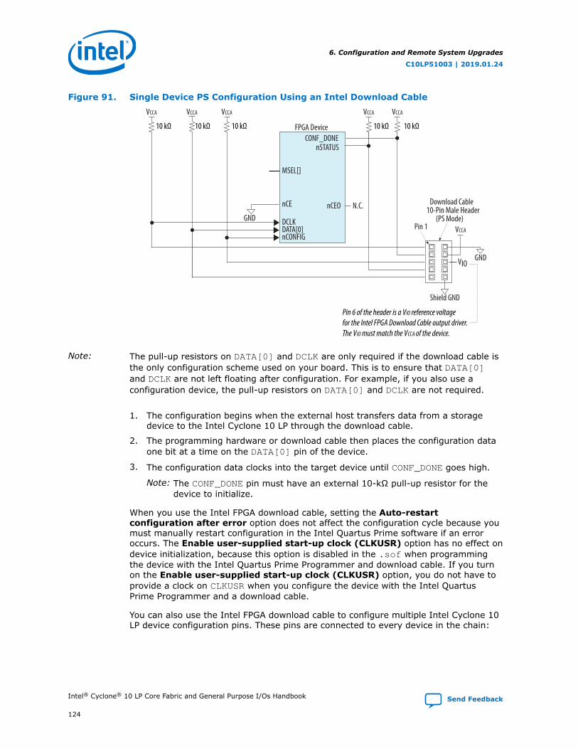
Figure 91. Single Device PS Configuration Using an Intel Download Cable
Download Cable 10-Pin Male Header
(PS Mode)
VCCA VCCA VCCA VCCA
VCCA
VCCA
FPGA Device
DCLK
nCONFIG
CONF_DONE
Shield GND
10 kΩ
nSTATUS
DATA[0] Pin 1
nCE
GND
GND
nCEO N.C.
MSEL[]
10 kΩ 10 kΩ 10 kΩ 10 kΩ
VIO
Pin 6 of the header is a VIO reference voltage for the Intel FPGA Download Cable output driver. The VIO must match the VCCA of the device.
Note: The pull-up resistors on DATA[0] and DCLK are only required if the download cable isthe only configuration scheme used on your board. This is to ensure that DATA[0]and DCLK are not left floating after configuration. For example, if you also use aconfiguration device, the pull-up resistors on DATA[0] and DCLK are not required.
1. The configuration begins when the external host transfers data from a storagedevice to the Intel Cyclone 10 LP through the download cable.
2. The programming hardware or download cable then places the configuration dataone bit at a time on the DATA[0] pin of the device.
3. The configuration data clocks into the target device until CONF_DONE goes high.
Note: The CONF_DONE pin must have an external 10-kΩ pull-up resistor for thedevice to initialize.
When you use the Intel FPGA download cable, setting the Auto-restartconfiguration after error option does not affect the configuration cycle because youmust manually restart configuration in the Intel Quartus Prime software if an erroroccurs. The Enable user-supplied start-up clock (CLKUSR) option has no effect ondevice initialization, because this option is disabled in the .sof when programmingthe device with the Intel Quartus Prime Programmer and download cable. If you turnon the Enable user-supplied start-up clock (CLKUSR) option, you do not have toprovide a clock on CLKUSR when you configure the device with the Intel QuartusPrime Programmer and a download cable.
You can also use the Intel FPGA download cable to configure multiple Intel Cyclone 10LP device configuration pins. These pins are connected to every device in the chain:
6. Configuration and Remote System Upgrades
C10LP51003 | 2019.01.24
Intel® Cyclone® 10 LP Core Fabric and General Purpose I/Os Handbook Send Feedback
124

• nCONFIG
• nSTATUS
• DCLK
• DATA[0]
• CONF_DONE
All devices in the chain utilize and enter user mode at the same time because all theCONF_DONE pins are tied together. The entire chain halts configuration if any devicedetects an error because the nSTATUS pins are tied together.
6.1.2.4. Passive Serial Multi-Device Configuration Using a Download Cable
You can also use a download cable to configure multiple Intel Cyclone 10 LP deviceconfiguration pins.
The download cable could be an Intel FPGA download cable or Intel FPGA Ethernetcable.
Note: Power up the VCC of the Intel FPGA download cable with a 2.5-V supply from VCCA.Third-party programmers must switch to 2.5 V.
Figure 92. Multiple Device PS Configuration Using an Intel FPGA Download Cable
FPGA Device 1
FPGA Device 2
nCE
nCONFIG
CONF_DONE
DCLK
nCE
nCONFIG
CONF_DONE
DCLK
nCEO
GND
(PS Mode)
nSTATUS
nSTATUS
DATA0
DATA0
GND
10 kΩ
Pin 1
Download Cable10-Pin Male Header
nCEO N.C.
GNDMSEL[2..0]
MSEL[2..0]
VCCA
10 kΩ
VCCA10 kΩ
VCCIO
VCCA
VCCA
VCCA
VCCA
10 kΩ
10 kΩ
10 kΩ
VIO
6. Configuration and Remote System Upgrades
C10LP51003 | 2019.01.24
Send Feedback Intel® Cyclone® 10 LP Core Fabric and General Purpose I/Os Handbook
125

Note: The pull-up resistors on DATA[0] and DCLK are only required if the download cable isthe only configuration scheme used on your board. This is to ensure that DATA[0]and DCLK are not left floating after configuration. For example, if you also use aconfiguration device, the pull-up resistors on DATA[0] and DCLK are not required.
When a device completes configuration, its nCEO pin is released low to activate thenCE pin of the next device. Configuration automatically begins for the second device.
6.1.3. Fast Passive Parallel Configuration
The FPP configuration scheme uses an external host, such as a microprocessor, MAX IIdevice, or MAX V device. This scheme allows for a faster configuration time.
You can use an external host to control the transfer of configuration data from anexternal storage such as flash memory to the FPGA. The design that controls theconfiguration process resides in the external host. You can store the configuration datain Raw Binary File (.rbf), Hexadecimal (Intel-Format) File (.hex), or Tabular Text File(.ttf) formats.
You can use the PFL IP core with a MAX II or MAX V device to read configuration datafrom the flash memory device and configure the Intel Cyclone 10 LP device.
Note: 1. Two DCLK falling edges are required after the CONF_DONE pin goes high to beginthe initialization of the device.
2. The FPP configuration is not supported in E144 package of Intel Cyclone 10 LPdevices.
3. Intel Cyclone 10 LP devices do not support enhanced configuration devices for FPPconfiguration.
Related Information
Parallel Flash Loader IP Core User GuideProvides more information about how to instantiate the Parallel Flash Loader (PFL)IP core in your design, programming flash memory, and configuring your FPGAfrom the flash memory.
FPP Configuration Guidelines
Consider the following guidelines when you configure the Intel Cyclone 10 LP devices:
• Connect the pull-up resistors of the FPGA device to the VCC supply of the bank inwhich the pin resides.
• You can leave the nCEO pin unconnected or use it as a user I/O pin when it doesnot feed the nCE pin of another device.
• The MSEL pin settings vary for different configuration voltage standards and PORtime.
• The nCSO and ASDO pins are dual-purpose I/O pins. The ASDO pin also functionsas the DATA[1] pin in FPP mode.
6. Configuration and Remote System Upgrades
C10LP51003 | 2019.01.24
Intel® Cyclone® 10 LP Core Fabric and General Purpose I/Os Handbook Send Feedback
126

• For multi-device configurations, connect the pull-up resistor of the slave FPGAdevice(s) to the VCCIO supply voltage of I/O bank in which the nCE pin resides.
• Connect the repeater buffers between the master and slave devices of the FPGAdevice for DATA[0] and DCLK. All I/O inputs must maintain a maximum ACvoltage of 4.1 V. The output resistance of the repeater buffers must fit themaximum overshoot equation.
• The 50 Ω series resistors are optional if the 3.3 V configuration voltage standard isapplied. For optimal signal integrity, connect these 50 Ω series resistors if the 2.5V or 3.0 V configuration voltage standard is applied.
6.1.3.1. Fast Passive Parallel Single-Device Configuration
To configure an Intel Cyclone 10 LP device, connect the device to an external host.
Figure 93. Single Device FPP Configuration Using an External Host
External Host(MAX II Device,
MAX V Device, orMicroprocessor
CONF_DONEnSTATUSnCE
DATA[7..0]nCONFIG
FPGA Device
Memory
ADDR
GND
10 kΩ
DCLK
nCEO N.C.
MSEL[3..0]
DATA[7..0]10 kΩ
VCCIO VCCIO
1. The configuration begins when nSTATUS releases and the Intel Cyclone 10 LPdevice is ready to receive configuration data.
2. When nSTATUS is high, the external host device places the configuration data onebyte at a time on DATA[7..0].
3. The Intel Cyclone 10 LP device receives configuration data on DATA[7..0] andclock on DCLK.
4. The configuration data latches onto the device on the rising edge of DCLK.
5. The data continuously clocks into the target device until CONF_DONE goes high.
Note: CONF_DONE goes high one byte early in FPP configuration mode. The lastbyte is required for serial configuration (AS and PS) modes.
6. When initialization completes, INIT_DONE releases and goes high. The externalhost device must be able to detect this low-to-high transition signal, whichindicates the device has entered user mode.
To ensure DCLK and DATA[0] are not left floating at the end of configuration, the MAXV device must drive them high or low, depending on your board. The DATA[0] pin isavailable as a user I/O pin after configuration.
6. Configuration and Remote System Upgrades
C10LP51003 | 2019.01.24
Send Feedback Intel® Cyclone® 10 LP Core Fabric and General Purpose I/Os Handbook
127

In the FPP scheme, the DATA[0] pin is tri-stated by default in user mode and must bedriven by the external host device. You change this default option by selecting theDual-Purpose Pins tab of the Device and Pin Options dialog box in the IntelQuartus Prime software.
• The configuration clock (DCLK) speed must be below the specified systemfrequency to ensure correct configuration.
• You can pause configuration by halting DCLK for an indefinite amount of timebecause there is no maximum DCLK period.
The external host device also monitors CONF_DONE and INIT_DONE to ensuresuccessful configuration.
• The CONF_DONE pin must be monitored by the external device to detect errorsand to determine when programming is complete.
• If all configuration data is sent, but CONF_DONE or INIT_DONE has not gonehigh, the external device must reconfigure the target device.
6.1.3.2. Fast Passive Parallel Multi-Device Configuration
To configure multiple devices using an external host, cascade the Intel Cyclone 10 LPdevices.
Figure 94. Multi-Device FPP Configuration Using an External Host
CONF_DONEnSTATUSnCE
nCONFIG
Memory
ADDR DATA[7..0]
GND
10 kΩ10 kΩ
DCLK
nCEO
CONF_DONEnSTATUSnCE
nCONFIGDCLK
nCEO
DATA[7..0]
MSEL[3..0]
DATA[7..0]
MSEL[3..0]
Buffers
External Host(MAX II Device,
MAX V Device, orMicroprocessor)
FPGA Device 1 FPGA Device 2
N.C.
10 kΩ
VCCIO VCCIO
VCCIO
1. After the first device completes configuration in a multi-device configuration chain,its nCEO pin drives low to activate the nCE pin of the second device prompting itto begin configuration.
2. The second device in the chain begins configuration in one clock cycle. Thedestinations of data transfer is transparent to the external host device. ThenCONFIG, nSTATUS, DCLK, DATA[7..0], and CONF_DONE configuration pins are
6. Configuration and Remote System Upgrades
C10LP51003 | 2019.01.24
Intel® Cyclone® 10 LP Core Fabric and General Purpose I/Os Handbook Send Feedback
128

connected to every device in the chain. To ensure signal integrity and preventclock skew problems, configuration signals may require buffering. Ensure thatDCLK and DATA lines are buffered.
3. All devices initialize and enter user mode at the same time because all theCONF_DONE pins are tied together.
4. If any device detects an error, configuration stops for the entire chain and youmust reconfigure the entire chain because all nSTATUS and CONF_DONE pins aretied together. For example, if the first device flags an error on nSTATUS, it resetsthe chain by pulling its nSTATUS pin low. This behavior is similar to a single devicedetecting an error.
6.1.3.2.1. Fast Passive Parallel Multi Devices Using Same Configuration Data
You can have multiple devices that contain the same configuration data in yoursystem.
Figure 95. Multiple Device FPP Configuration When Both Devices Receive the SameConfiguration Data
nCONFIG
Memory
ADDR DATA[7..0]
DCLK
nCEO N.C.
nCONFIGDCLK
nCEO N.C.
MSEL[3..0] MSEL[3..0]
VCCIO VCCIO
10 kΩ 10 kΩ
GND GND
CONF_DONE CONF_DONEnSTATUS nSTATUSnCE nCE
DATA[7..0] DATA[7..0]
Buffers
External Host(MAX II Device,
MAX V Device, orMicroprocessor)
FPGA Device 1 FPGA Device 2
The nCE pins of the device in the chain are connected to GND, allowing configurationfor these devices to begin and end at the same time. nCONFIG, nSTATUS, DCLK,DATA[0], and CONF_DONE configuration pins are connected to every device in thechain.
To ensure signal integrity and prevent clock skew problems, configuration signals mayrequire buffering. Ensure that the DCLK and DATA lines are buffered.
6.1.4. JTAG Configuration
In Intel Cyclone 10 LP devices, JTAG instructions take precedence over otherconfiguration schemes.
JTAG configuration can take place without waiting for other configuration modes tocomplete. For example, if you attempt JTAG configuration in Intel Cyclone 10 LPdevices during PS configuration, PS configuration terminates and JTAG configurationbegins. If the MSEL pins are set to AS mode, the Intel Cyclone 10 LP device does nottransmit a DCLK signal when JTAG configuration takes place.
6. Configuration and Remote System Upgrades
C10LP51003 | 2019.01.24
Send Feedback Intel® Cyclone® 10 LP Core Fabric and General Purpose I/Os Handbook
129

JTAG has developed a specification for boundary-scan testing (BST). The BSTarchitecture offers the capability to efficiently test components on PCBs with tight leadspacing. The BST architecture can test pin connections without using physical testprobes and capture functional data while a device is normally operating. You can alsouse the JTAG circuitry to shift configuration data into the device.
The Intel Quartus Prime software generates an .sof that you can use for JTAGconfiguration using a download cable in the Intel Quartus Prime software programmer.
Table 40. Dedicated JTAG Pins
Pin Name Pin Type Description
TDI Test data input • Serial input pin for instructions, and test andprogramming data.
• Data shifts in on the rising edge of TCK.• If the JTAG interface is not required on the board, JTAG
circuitry is disabled by connecting this pin to VCC.• TDI pin has weak internal pull-up resistors (typically
25kΩ).
TDO Test data output • Serial data output pin for instructions, and test andprogramming data.
• Data shifts out on the falling edge of TCK. The pin is tri-stated if data is not being shifted out of the device.
• If the JTAG interface is not required on the board, theJTAG circuitry is disabled by leaving this pinunconnected.
TMS Test mode select • Input pin that provides the control signal to determinethe transitions of the TAP controller state machine.
• Transitions in the state machine occur on the rising edgeof TCK. Therefore, TMS must be set up before the risingedge of TCK. TMS is evaluated on the rising edge of TCK.
• If the JTAG interface is not required on the board, theJTAG circuitry is disabled by connecting this pin to VCC.
• TMS pin has weak internal pull-up resistors (typically 25kΩ).
TCK Test clock input • The clock input to the BST circuitry.• Some operations occur at the rising edge, while others
occur at the falling edge.• If the JTAG interface is not required on the board, the
JTAG circuitry is disabled by connecting this pin to GND.• The TCK pin has an internal weak pull-down resistor.
You can download data to the device through the Intel FPGA download cable or theIntel FPGA Ethernet cable during JTAG configuration. Configuring devices with a cableis similar to programming devices in-system.
Alternatively, you can use the JRunner software with .rbf or a JAM™ Standard Testand Programming Language (STAPL) Format File (.jam) or JAM Byte Code File (.jbc)with other third-party programmer tools.
Note: You cannot use the Intel Cyclone 10 LP decompression if you are configuring yourIntel Cyclone 10 LP device using JTAG-based configuration.
6. Configuration and Remote System Upgrades
C10LP51003 | 2019.01.24
Intel® Cyclone® 10 LP Core Fabric and General Purpose I/Os Handbook Send Feedback
130

JTAG Configuration Connection Guidelines
Consider the following guidelines when you configure the Intel Cyclone 10 LP devices:
• Connect the pull-up resistors of the FPGA device to the VCC supply of the bank inwhich the pin resides.
• You can leave the nCEO pin unconnected or use it as a user I/O pin when it doesnot feed the nCE pin of another device.
• The MSEL pin settings vary for different configuration voltage standards and PORtime.
• The nCSO and ASDO pins are dual-purpose I/O pins. The ASDO pin also functionsas the DATA[1] pin in FPP mode.
• For multi-device configurations, connect the pull-up resistor of the slave FPGAdevice(s) to the VCCIO supply voltage of I/O bank in which the nCE pin resides.
• Connect the repeater buffers between the master and slave devices of the FPGAdevice for DATA[0] and DCLK. All I/O inputs must maintain a maximum ACvoltage of 4.1 V. The output resistance of the repeater buffers must fit themaximum overshoot equation.
• The 50 Ω series resistors are optional if the 3.3 V configuration voltage standard isapplied. For optimal signal integrity, connect these 50 Ω series resistors if the 2.5V or 3.0 V configuration voltage standard is applied.
6.1.4.1. Configuring Intel Cyclone 10 LP Devices with the JRunner SoftwareDriver
The JRunner software driver allows you to configure Intel Cyclone 10 LP devicesthrough the Intel FPGA download cable in JTAG mode.
The supported programming input file is in .rbf format. The JRunner software driveralso requires a Chain Description File (.cdf) generated by the Intel Quartus Primesoftware. The JRunner software driver is specifically for embedded JTAG configuration.You can customize the code to make it run on your embedded platform.
Note: The .rbf used by the JRunner software driver cannot be a compressed .rbf becausethe JRunner software driver uses JTAG-based configuration. During JTAG-basedconfiguration, the real-time decompression feature is not available.
6.1.4.2. Configuring Intel Cyclone 10 LP Devices with Jam STAPL
Jam* STAPL supports programming or configuration of programmable devices andtesting of electronic systems, using the IEEE 1149.1 JTAG interface
Jam STAPL, JEDEC standard JESD-71, is a standard file format for in-systemprogrammability (ISP) purposes. Jam STAPL is a freely licensed open standard. TheJam Player provides an interface for manipulating the IEEE Std. 1149.1 JTAG TAP statemachine.
6. Configuration and Remote System Upgrades
C10LP51003 | 2019.01.24
Send Feedback Intel® Cyclone® 10 LP Core Fabric and General Purpose I/Os Handbook
131

6.1.4.3. JTAG Single-Device Configuration
To configure a single device in a JTAG chain, the programing software sets the otherdevices to bypass mode. A device in a bypass mode transfers the programming datafrom the TDI pin to the TDO pin through a single bypass register. The configurationdata is available on the TDO pin one clock cycle later.
The Intel Quartus Prime software uses the CONF_DONE pin to verify the completion ofthe configuration process through the JTAG port:
• CONF_DONE pin is low—indicates that configuration has failed.
• CONF_DONE pin is high—indicates that configuration was successful.
After the configuration data is transmitted serially using the JTAG TDI port, the TCKport clocks additional cycles to perform device initialization.
To configure Intel Cyclone 10 LP device using an Intel FPGA download cable, connectthe device as shown in the following figure.
• For device using VCCIO of 2.5, 3.0, and 3.3 V, all I/O inputs must maintain amaximum AC voltage of 4.1 V because JTAG pins do not have the internal PCIclamping diodes to prevent voltage overshoot. You must power up the VCC of thedownload cable with a 2.5-V supply from VCCA
• For device using VCCIO of 1.2 V, 1.5 V, and 1.8 V, you can power up the VCC of thedownload cable with the supply from VCCIO.
Figure 96. JTAG Configuration of a Single Device Using a Download Cable
Download Cable 10-Pin Male Header
(JTAG Mode) (Top View)
FPGA Device
nCONFIGCONF_DONE
GNDGND
nSTATUSTDI
TMS
TDOTCK
Pin 1
nCE
GND
GND
nCEON.C.
MSEL[]DATA[0]DCLK
VIO
VCCIO VCCIO
10 kΩ 10 kΩ
VCCA/VCCIO
1 kΩ
If you only use the JTAG configuration, connect nCONFIG to logic high and MSEL pins to GND. Pull DCLK and DATA[0] either high or low, whichever is convenient on your board. If you are using JTAG in conjunction with another configuration scheme, connect MSEL, nCONFIG, and DCLK based on the selected configuration scheme.
VCCA/VCCIO
VCCA/VCCIO
6. Configuration and Remote System Upgrades
C10LP51003 | 2019.01.24
Intel® Cyclone® 10 LP Core Fabric and General Purpose I/Os Handbook Send Feedback
132

To configure Intel Cyclone 10 LP device using a microprocessor, connect the device asshown in the following figure.
Figure 97. JTAG Configuration of a Single Device Using a Microprocessor
Microprocessor
CONF_DONEnSTATUS
FPGA Device
Memory
ADDR
nCONFIGDATA[0]DCLK
MSEL[]
DATA
TCKTMSTDO
TDI
10 kΩ10 kΩ
VCCIO VCCIO
Connect nCE to GND or drive it lowfor succesful JTAG configuration.
All I/O inputs must maintain a maximum AC voltage of 4.1 V.
nCE
GNDnCEON.C.
Note: Connect the nCONFIG and MSEL pins to support a non-JTAG configuration scheme. Ifyou only use a JTAG configuration, connect the nCONFIG pin to logic-high and theMSEL pins to GND. Pull DCLK and DATA[0] to either high or low, whichever isconvenient on your board.
6.1.4.4. JTAG Multi-Device Configuration
You can configure multiple devices in a JTAG chain.
The CONF_DONE and nSTATUS signals are shared in multi-device AS, PS, and FPPconfiguration chains to ensure that the devices enter user mode at the same timeafter configuration is complete. When the CONF_DONE and nSTATUS signals areshared among all the devices, you must configure every device when JTAGconfiguration is performed.
1. After the first device completes configuration in a multi-device configuration chain,its nCEO pin drives low to activate the nCE pin of the second device prompting itto begin configuration.
2. The second device in the chain begins configuration. If both devices are also in aJTAG chain, ensure that the nCE pins are connected to GND during JTAGconfiguration or that the devices are JTAG-configured in the same order as theconfiguration chain.
3. As long as the devices are JTAG configured in the same order as the multi-deviceconfiguration chain, the nCEO pin of the previous device drives the nCE pin of thenext device low when it has successfully been JTAG-configured.
4. Place other Intel devices that have JTAG support in the same JTAG chain for deviceprogramming and configuration.
To configure an Intel Cyclone 10 LP device using a download cable, connect the deviceas shown in the following figure.
6. Configuration and Remote System Upgrades
C10LP51003 | 2019.01.24
Send Feedback Intel® Cyclone® 10 LP Core Fabric and General Purpose I/Os Handbook
133

• For device using VCCIO of 2.5, 3.0, and 3.3 V:
— All I/O inputs must maintain a maximum AC voltage of 4.1 V because JTAGpins do not have the internal PCI clamping diodes to prevent voltageovershoot.
— You must power up the VCC of the download cable with a 2.5-V supply fromVCCA.
• For device using VCCIO of 1.2, 1.5, and 1.8 V:
— You can power up the VCC of the download cable with the supply from VCCIO.
— In the Intel FPGA download cable and Intel FPGA parallel port cable, this pin isconnected to nCE when it is used for AS programming, otherwise it is notconnected.
Figure 98. JTAG Configuration of Multiple Devices Using a Download Cable
TMS TCK
Download Cable 10-Pin Male Header
(JTAG Mode)
Pin 1
nSTATUSnCONFIG
VCCIO VCCIO VCCIO
CONF_DONEMSEL[]nCEO nCEO nCEO
FPGA Device FPGA Device FPGA Device
1 kΩ
10 kΩ 10 kΩ 10 kΩ 10 kΩ 10 kΩ 10 kΩ
DCLK
nCE
GND
TMS TCK
nSTATUSnCONFIG
MSEL[]CONF_DONEDCLK
GND
nCE
TMS TCKTDI TDO TDI TDO TDI TDO
nSTATUSnCONFIG
MSEL[]CONF_DONEDCLK
GND
nCE
The resistor value can vary from 1 kΩ to 10kΩ.
VCCA/VCCIO
VCCA/VCCIO
VCCA/VCCIO
VCCIO VCCIOVCCIO
Note: Connect the nCONFIG and MSEL pins to support a non-JTAG configuration scheme. Ifyou only use a JTAG configuration, connect the nCONFIG pin to logic-high and theMSEL pins to GND. Pull DCLK and DATA[0] to either high or low, whichever isconvenient on your board.
6.1.4.5. Combining JTAG and AS Configuration Schemes
You can combine the AS configuration scheme with the JTAG-based configuration.
This setup uses two 10-pin download cable headers on the board.
• One download cable is used in JTAG mode to configure the Intel Cyclone 10 LPdevice directly through the JTAG interface.
• The other download cable is used in AS mode to program the serial configurationdevice in-system through the AS programming interface.
If you try configuring the device using both schemes simultaneously, JTAGconfiguration takes precedence and AS configuration terminates.
6. Configuration and Remote System Upgrades
C10LP51003 | 2019.01.24
Intel® Cyclone® 10 LP Core Fabric and General Purpose I/Os Handbook Send Feedback
134

Figure 99. Combining JTAG and AS Configuration Schemes
DATADCLK
nCSASDI
Serial ConfigurationDevice
FPGA Device 10 kΩ10 kΩ
VCCIO VCCIO
GND
nCEO
nCE
nSTATUSCONF_DONE
10 kΩ
VCCIO
nCONFIG
MSEL[ ]10 kΩ
VCCA
N.C.
VCCA
TCKTDOTMS
TDI
CLKUSR
GND
VCCA
3.3 VPin 1
Pin 1
Download Cable(JTAG Mode)
10-Pin Male Header (top view)
Download Cable(AS Mode)
10-Pin Male Header
3.3 V
10 pf GND
GND
10 pf10 pf
GND
10 pf
GND
(6)
3.3 V 3.3 V3.3 V
DATA[0]DCLKnCSOASDO
1 kΩ
You must place the diodes and capacitors as close as possible to the FPGA device. Intel recommends using the Schottky diode, which has a relatively lower forward diode voltage (VF) than the switching and Zener diodes, for effective voltage clamping.
These pins are dual-purpose I/O pins. The ASDO pin functions as DATA[1] pin in FPP mode.
Resistor value can vary from 1 kΩ to 10 kΩ.
6.1.4.6. Programming Serial Configuration Devices In-System with the JTAGInterface
Intel Cyclone 10 LP devices in a single- or multiple-device chain support in-systemprogramming of a serial configuration device with the JTAG interface through the SFLdesign.
The intelligent host or download cable of the board can use the four JTAG pins on theIntel Cyclone 10 LP device to program the serial configuration device in system, evenif the host or download cable cannot access the configuration pins (DCLK, DATA, ASDI,and nCS).
The SFL design is a JTAG-based in-system programming solution for Intel serialconfiguration devices. The SFL is a bridge design for the Intel Cyclone 10 LP devicethat uses its JTAG interface to access the JTAG Indirect Configuration DeviceProgramming (.jic) file and then uses the AS interface to program the serialconfiguration device. In a multiple device chain, you must only configure the masterdevice that controls the serial configuration device. Slave devices in the multiple
6. Configuration and Remote System Upgrades
C10LP51003 | 2019.01.24
Send Feedback Intel® Cyclone® 10 LP Core Fabric and General Purpose I/Os Handbook
135

device chain that are configured by the serial configuration device do not have to beconfigured when using this feature. To successfully use this feature, set the MSEL pinsof the master device to select the AS configuration scheme.
The serial configuration device in-system programming through the Intel Cyclone 10LP device JTAG interface has three stages:
• Loading the SFL design
• Configuring the device
• Reconfiguring the device
6.1.4.6.1. Loading the SFL Design
The intelligent host uses the JTAG interface to configure the master device with an SFLdesign.
The SFL design bridges the JTAG interface and AS interface with glue logic. The SFLdesign allows the master device to control the access of four serial configurationdevice pins or Active Serial Memory Interface (ASMI) pins, through the JTAG interface.The ASMI pins are serial clock input (DCLK), serial data output (DATA), AS data input(ASDI), and active-low chip select (nCS) pins.
If you configure a master device with an SFL design, the master device enters usermode even though the slave devices in the multiple device chain are not beingconfigured. The master device enters user mode with a SFL design even though theCONF_DONE signal is externally held low by the other slave devices in chain.
Figure 100. Programming Serial Configuration Devices In-System Using the JTAGInterface
nCE
MSEL[ ]nCONFIGCONF_DONE
VCCA
VCCA
VCCIO
GND
GND GND
GND
VCCIO
VCCA
1 kΩ
10 kΩ10 kΩ
nSTATUS
Pin 1
Download Cable 10-Pin MaleHeader (Top View)
TCKTDO
TMSTDI
CLKUSR
FPGA Device
nCEON.C.
DCLK
DATA[0]
nCSOASDO
DCLK
DATA
nCS
ASDI
Serial Configuration Device
VCCIO
10 kΩ
SerialFlash
Loader25 Ω
The resistor value can vary from 1 kΩ to 10 kΩ.
These pins are dual-purpose I/O pins. The ASDO pin functions as DATA[1] pin in FPP mode.
Connect the series resistor at the near end of the
serial configuration device.
6.1.4.6.2. Configuring the Device
In the second stage, the SFL design in the master device enables you to write theconfiguration data for the device chain into the serial configuration device with theIntel Cyclone 10 LP device JTAG interface.
6. Configuration and Remote System Upgrades
C10LP51003 | 2019.01.24
Intel® Cyclone® 10 LP Core Fabric and General Purpose I/Os Handbook Send Feedback
136

The JTAG interface sends the programming data for the serial configuration device tothe Intel Cyclone 10 LP device first. The Intel Cyclone 10 LP device then uses theASMI pins to send the data to the serial configuration device.
6.1.4.6.3. Reconfiguring the Device
After the configuration data is successfully written into the serial configuration device,the Intel Cyclone 10 LP device does not automatically start reconfiguration.
The intelligent host issues the PULSE_NCONFIG JTAG instruction to initialize thereconfiguration process. During reconfiguration, the master device resets and the SFLdesign no longer exists in the Intel Cyclone 10 LP device and the serial configurationdevice configures all the devices in the chain with the user design.
6.1.4.7. JTAG Instructions
You can perform JTAG testing on Intel Cyclone 10 LP devices before, during, and afterconfiguration using the JTAG instructions.
Intel Cyclone 10 LP devices support the BYPASS, IDCODE, and SAMPLE instructionsduring configuration without interrupting configuration.
All other JTAG instructions can only be issued by first interrupting configuration andreprogramming I/O pins with the ACTIVE_DISENGAGE and CONFIG_IO instructions.
• The CONFIG_IO instruction configures the I/O buffers through the JTAG port andinterrupts configuration when issued after the ACTIVE_DISENGAGE instruction.This instruction allows you to perform board-level testing prior to configuring theIntel Cyclone 10 LP device or waiting for a configuration device to completeconfiguration.
• Before issuing the CONFIG_IO instruction, you must issue theACTIVE_DISENGAGE instruction. In Intel Cyclone 10 LP devices, the CONFIG_IOinstruction does not hold nSTATUS low until reconfiguration, so you mustdisengage the active configuration mode controller when active configuration isinterrupted. The ACTIVE_DISENGAGE instruction places the active configurationmode controllers in an idle state before JTAG programming.
The ACTIVE_ENGAGE instruction allows you to re-engage a disengaged activeconfiguration mode controller.
6.1.4.7.1. CONFIG_IO
Use the CONFIG_IO instruction to reconfigure the I/O configuration shift register(IOCSR) chain.
This instruction allows you to perform board-level testing before configuring the IntelCyclone 10 LP device or waiting for a configuration device to complete configuration.After the configuration is interrupted and JTAG testing is complete, you mustreconfigure the part through the PULSE_NCONFIG JTAG instruction or by pulsing thenCONFIG pin low.
You can issue the CONFIG_IO instruction any time during user mode.
You must meet the following timing restrictions when using the CONFIG_IOinstruction:
6. Configuration and Remote System Upgrades
C10LP51003 | 2019.01.24
Send Feedback Intel® Cyclone® 10 LP Core Fabric and General Purpose I/Os Handbook
137

• The CONFIG_IO instruction cannot be issued when the nCONFIG pin is low.
• You must observe a 230µs minimum wait time after any of the followingconditions:
— nCONFIG pin goes high
— Issue the PULSE_NCONFIG instruction
— Issue the ACTIVE_ENGAGE instruction, before issuing the CONFIG_IOinstruction
• You must wait 230 µs after power up, with the nCONFIG pin high before issuingthe CONFIG_IO instruction (or wait for the nSTATUS pin to go high).
Use the ACTIVE_DISENGAGE instruction with the CONFIG_IO instruction to interruptconfiguration.
Table 41. JTAG CONFIG_IO (without JTAG_PROGRAM) Instruction FlowsThe table below lists the sequence of instructions to use for various CONFIG_IO usage scenarios. The listshows the configuration scheme and current state of the device.
Note: R indicates that the instruction must be executed before the next instruction, O indicates theoptional instruction, A indicates that the instruction must be executed, and NA indicates thatthe instruction is not allowed in this mode.
JTAG Instruction Prior to UserMode(Interrupting
Configuration)
User Mode Power Up
PS FPP AS PS FPP AS PS FPP AS
ACTIVE_DISENGAGE O O O O O O – – –
CONFIG_IO R R R R R R NA NA NA
JTAG Boundary ScanInstructions (noJTAG_PROGRAM)
O O O O O O – – –
ACTIVE_ENGAGE
A A
R (27)
A A
R (27) – – –
PULSE_nCONFIG A (28) O – – –
Pulse nCONFIG pin A (28) O – – –
JTAG TAP Reset R R R R R R – – –
The CONFIG_IO instruction does not hold nSTATUS low until reconfiguration. Youmust disengage the AS configuration controller by issuing the ACTIVE_DISENGAGEand ACTIVE_ENGAGE instructions when active configuration is interrupted. You mustissue the ACTIVE_DISENGAGE instruction alone or prior to the CONFIG_IO instructionif the JTAG_PROGRAM instruction is to be issued later. This puts the activeconfiguration controllers into the idle state. The active configuration controller isreengaged after user mode is reached through JTAG programming.
Note: While executing the CONFIG_IO instruction, all user I/Os are tri-stated.
(27) Required if you use ACTIVE_ENGAGE.
(28) Not required if you use ACTIVE_ENGAGE.
6. Configuration and Remote System Upgrades
C10LP51003 | 2019.01.24
Intel® Cyclone® 10 LP Core Fabric and General Purpose I/Os Handbook Send Feedback
138

If reconfiguration after interruption is performed using configuration modes (ratherthan using JTAG_PROGRAM), it is not necessary to issue the ACTIVE_DISENGAGEinstruction prior to CONFIG_IO. You can start reconfiguration by either pullingnCONFIG low for at least 500 ns or issuing the PULSE_NCONFIG instruction. If theACTIVE_DISENGAGE instruction was issued and the JTAG_PROGRAM instruction failsto enter user mode, you must issue the ACTIVE_ENGAGE instruction to reactivate theactive configuration controller. Issuing the ACTIVE_ENGAGE instruction also triggersreconfiguration in configuration modes; therefore, it is not necessary to pull nCONFIGlow or issue the PULSE_NCONFIG instruction.
6.1.4.7.2. ACTIVE_DISENGAGE
The ACTIVE_DISENGAGE instruction places the active configuration controller (AS)into an idle state prior to JTAG programming.
You place the active controller in an idle state for two reasons:
• To ensure that it is not trying to configure the device during JTAG programming.
• To allow the controllers to properly recognize a successful JTAG programming thatresults in the device reaching user mode.
The ACTIVE_DISENGAGE instruction is required before JTAG programming regardlessof the current state of the Intel Cyclone 10 LP device if the MSEL pins are set to an ASconfiguration scheme. If the ACTIVE_DISENGAGE instruction is issued during apassive configuration scheme (PS or FPP), it has no effect on the Intel Cyclone 10 LPdevice. Similarly, the CONFIG_IO instruction is issued after an ACTIVE_DISENGAGEinstruction, but is no longer required to properly halt configuration.
Table 42. JTAG Programming Instruction FlowsThe table below lists the required, recommended, and optional instructions for each configuration mode. Theordering of the required instructions is a hard requirement and must be met to ensure functionality. The listshows the configuration scheme and current state of the device.
Note: R indicates that the instruction must be executed before the next instruction, O indicates theoptional instruction, Rc indicates the recommended instruction, and NA indicates that theinstruction is not allowed in this mode.
JTAG Instruction Prior to UserMode(Interrupting
Configuration)
User Mode Power Up
PS FPP AS PS FPP AS PS FPP AS
ACTIVE_DISENGAGE O O R O O O O O R
CONFIG_IO Rc Rc O O O O NA NA NA
Other JTAGInstructions
O O O O O O O O O
JTAG_PROGRAM R R R R R R R R R
CHECK_STATUS Rc Rc Rc Rc Rc Rc Rc Rc Rc
JTAG_STARTUP R R R R R R R R R
JTAG TAP Reset/Other Instructions
R R R R R R R R R
In the AS configuration scheme, the ACTIVE_DISENGAGE instruction puts the activeconfiguration controller into idle state.
6. Configuration and Remote System Upgrades
C10LP51003 | 2019.01.24
Send Feedback Intel® Cyclone® 10 LP Core Fabric and General Purpose I/Os Handbook
139

• If a successful JTAG programming is executed, the active controller isautomatically re-engaged after user mode is reached through JTAG programming.This causes the active controller to transition to their respective user mode states.
• If JTAG programming fails to get the Intel Cyclone 10 LP device to enter usermode and re-engage active programming, you can re-engage the AS controller bymoving the JTAG TAP controller to the reset state or by issuing theACTIVE_ENGAGE instruction.
6.1.4.7.3. ACTIVE_ENGAGE
The ACTIVE_ENGAGE instruction allows you to re-engage a disengaged activecontroller.
You can issue this instruction any time during configuration or user mode to reengagean already disengaged active controller, as well as trigger reconfiguration of the IntelCyclone 10 LP device in the active configuration scheme. The ACTIVE_ENGAGEinstruction functions as the PULSE_NCONFIG instruction when the device is in the PSor FPP configuration schemes. The nCONFIG pin is disabled when theACTIVE_ENGAGE instruction is issued.
Note: Intel does not recommend using the ACTIVE_ENGAGE instruction, but it is provided asa fail-safe instruction for re-engaging the active configuration controller (AS).
6.1.4.7.4. Overriding the Internal Oscillator
EN_ACTIVE_CLK and DIS_ACTIVE_CLK enable you to override the internal oscillatorduring the active configuration scheme.
The AS configuration controllers use the internal oscillator as the clock source. You canchange the clock source to CLKUSR through the JTAG instruction.
The EN_ACTIVE_CLK and DIS_ACTIVE_CLK JTAG instructions toggle on or offwhether or not the active clock is sourced from the CLKUSR pin or the internalconfiguration oscillator. To source the active clock from the CLKUSR pin, issue theEN_ACTIVE_CLK instruction. The CLKUSR pin becomes the active clock source.
When using the EN_ACTIVE_CLK instruction, you must enable the internal oscillatorfor the clock change to occur. By default, the configuration oscillator is disabled afterconfiguration and initialization is complete as well as the device has entered usermode. However, the internal oscillator is enabled in user mode by any of the followingconditions:
• A reconfiguration event (e.g. driving the nCONFIG pin to go low)
• Remote update is enabled
• Error detection is enabled
Note: When using the EN_ACTIVE_CLK and DIS_ACTIVE_CLK JTAG instructions to overridethe internal oscillator, you must clock the CLKUSR pin at two times the expected DCLKfrequency. The CLKUSR pin allows a maximum frequency of 40 MHz (40 MHz DCLK).
Normally, a test instrument uses the CLKUSR pin when it wants to drive its own clockto control the AS state machine. To revert the clock source back to the configurationoscillator, issue the DIS_ACTIVE_CLK instruction. After you issue theDIS_ACTIVE_CLK instruction, you must continue to clock the CLKUSR pin for 10 clock
6. Configuration and Remote System Upgrades
C10LP51003 | 2019.01.24
Intel® Cyclone® 10 LP Core Fabric and General Purpose I/Os Handbook Send Feedback
140

cycles. Otherwise, even toggling the nCONFIG pin does not revert the clock sourceand reconfiguration does not occur. A POR reverts the clock source back to theconfiguration oscillator. Toggling the nCONFIG pin or driving the JTAG state machine toreset state does not revert the clock source.
EN_ACTIVE_CLKThe DIS_ACTIVE_CLK instruction breaks the CLKUSR enable latch set by theEN_ACTIVE_CLK instruction and causes the clock source to revert back to the internaloscillator.
After the DIS_ACTIVE_CLK instruction is issued, you must continue to clock theCLKUSR pin for 10 clock cycles.
DIS_ACTIVE_CLKThe DIS_ACTIVE_CLK instruction breaks the CLKUSR enable latch set by theEN_ACTIVE_CLK instruction and causes the clock source to revert back to the internaloscillator.
After the DIS_ACTIVE_CLK instruction is issued, you must continue to clock theCLKUSR pin for 10 clock cycles.
6.2. Configuration Requirement
The Intel Cyclone 10 LP device have specific configuration pin requirements.
6.2.1. Power-On Reset (POR) Circuit
The POR circuit keeps the device in reset state until the power supply voltage levelshave stabilized during device power up.
After device power up, the device does not release nSTATUS until VCCINT, VCCA, andVCCIO (for I/O banks in which the configuration and JTAG pins reside) are above thePOR trip point of the device.
• VCCINT and VCCA are monitored for brown-out conditions after device power up.
• VCCA is the analog power to the phase-locked loop (PLL).
In some applications, it is necessary for a device to wake up very quickly to beginoperation. Intel Cyclone 10 LP devices offer the fast POR time option to support fastwake-up time applications. The fast POR time option has stricter power-uprequirements compared to the standard POR time option. You can select either thefast or standard POR option with the MSEL pin settings.
Note: If your system exceeds the fast or standard POR time, you must hold nCONFIG lowuntil all the power supplies are stable.
Related Information
Intel Cyclone 10 LP Device DatasheetProvides more information about the POR specifications.
6. Configuration and Remote System Upgrades
C10LP51003 | 2019.01.24
Send Feedback Intel® Cyclone® 10 LP Core Fabric and General Purpose I/Os Handbook
141

6.2.2. Configuration File Size
To calculate the amount of storage space required for multiple device configurations,add the file size of each device together.
Use the following data to estimate the file size before design compilation.
Note: Different configuration file formats, such as Hexadecimal (.hex) or Tabular Text File(.ttf) formats, have different file sizes. However, for any specific version of the IntelQuartus Prime software, any design targeted for the same device has the sameuncompressed configuration file size.
If you use compression, the file size varies after each compilation, because thecompression ratio depends on the design.
Table 43. Approximate Uncompressed Configuration Raw Binary File (.rbf) Sizes forIntel Cyclone 10 LP Devices
Device Data Size (bits)
10CL006 2,944,088
10CL010 2,944,088
10CL016 4,086,848
10CL025 5,748,552
10CL040 9,534,304
10CL055 14,889,560
10CL080 19,965,752
10CL120 28,571,696
6.2.3. Configuration and JTAG Pin I/O Requirements
Intel Cyclone 10 LP devices are manufactured using the TSMC 60-nm low-k dielectricprocess. Although the Intel Cyclone 10 LP devices use TSMC 2.5 V transistortechnology in the I/O buffers, the devices are compatible and able to interface with2.5 V, 3.0 V, and 3.3 V configuration voltage standards by following specificrequirements.
All I/O inputs must maintain a maximum AC voltage of 4.1 V.
• When using a serial configuration device in an AS configuration scheme, you mustconnect a 25 Ω series resistor for the DATA[0] pin.
• When cascading the Intel Cyclone 10 LP device family in a multi-deviceconfiguration for AS, FPP, and PS configuration schemes, you must connect therepeater buffers between the master and slave devices for the DATA and DCLKpins.
• When using the JTAG configuration scheme in a multi-device configuration,connect 25 Ω resistors on both ends of the TDO-TDI path if the TDO output driveris not an Intel Cyclone 10 LP device.
6. Configuration and Remote System Upgrades
C10LP51003 | 2019.01.24
Intel® Cyclone® 10 LP Core Fabric and General Purpose I/Os Handbook Send Feedback
142
The output resistance of the repeater buffers and the TDO path for all cases must fitthe maximum overshoot equation below:
0.8ZO ≤ RE ≤ 1.8ZO
Note: ZO is the transmission line impedance and RE is the equivalent resistance of the outputbuffer.
6.3. Configuration Details
This section describes the MSEL pin settings, configuration sequence, deviceconfiguration pins, configuration pin options, and configuration data compression.
6.3.1. MSEL Pin Settings
To select a configuration scheme, hardwire the MSEL pins to VCCA or GND withoutpull-up or pull-down resistors.
Table 44. MSEL Pin Settings for Each Configuration Scheme of Intel Cyclone 10 LPDevices with MSEL[3:0] Pins
ConfigurationScheme
Valid MSEL[3..0] POR Delay Configuration Voltage Standard (V)
AS 1101 Fast 3.3
0100 Fast 3.0
0010 Standard 3.3
0011 Standard 3.0
PS 1100 Fast 3.3/3.0/2.5
0000 Standard 3.3/3.0/2.5
FPP 1110 Fast 3.3/3.0/2.5
1111 Fast 1.8/1.5
Smaller Intel Cyclone 10 LP devices or package options (E144, M164, and U256) donot have the MSEL[3] pin. To configure these devices, select the MSEL[2:0] pinsaccording to the table below.
Table 45. MSEL Pin Settings for AS Configuration Scheme with MSEL[2:0] Pins
ConfigurationScheme
Valid MSEL[2..0] POR Delay Configuration Voltage Standard (V)
AS 101 Fast 3.3
010 Standard 3.3
011 Standard 3.0
PS 100 Fast 3.3/3.0/2.5
000 Standard 3.3/3.0/2.5
FPP 110 Fast 3.3/3.0/2.5
111 Fast 1.8/1.5
6. Configuration and Remote System Upgrades
C10LP51003 | 2019.01.24
Send Feedback Intel® Cyclone® 10 LP Core Fabric and General Purpose I/Os Handbook
143

Note: The configuration voltage standard applies to the VCCIO supply of the bank in whichthe configuration pins reside.
For JTAG-based configuration schemes, the MSEL pin settings are ignored. Do notleave the MSEL pins floating. Connect them to Vcca or GND. These pins support thenon-JTAG configuration scheme used in production. Intel recommends you connect theMSEL pins to GND if your device is only using JTAG configuration.
Note: You must also select the configuration scheme in the Configuration page of theDevice and Pin Options dialog box in the Intel Quartus Prime software. Based onyour selection, the option bit in the programming file is set accordingly.
6. Configuration and Remote System Upgrades
C10LP51003 | 2019.01.24
Intel® Cyclone® 10 LP Core Fabric and General Purpose I/Os Handbook Send Feedback
144

6.3.2. Configuration Sequence
The configuration process flow includes power up, reset, configuration, andinitialization.
Figure 101. Configuration Sequence for Intel Cyclone 10 LP DevicesThe figure describes the configuration sequence and each configuration stage.
Power supplies including VCCPGM reach recommended operating voltage
nSTATUS and nCONFIG released highCONF_DONE pulled low
CONF_DONE released high
INIT_DONE released high(if option enabled)
Power Up
• nSTATUS and CONF_DONE driven low
• All I/Os pins are tied to an internal weak pull-up
• Clears configuration RAM bits
Reset
• nSTATUS and CONF_DONE remain low
• All I/Os pins are tied to an internal weak pull-up
• Samples MSEL pins
Initialization
• Initializes internal logic and registers
• Enables I/O buffers
Configuration Error Handling
• nSTATUS pulled low• CONF_DONE remains low• Restarts configuration if option
enabled
User Mode
Executes your design
Configuration
Writes configuration data to FPGA
6. Configuration and Remote System Upgrades
C10LP51003 | 2019.01.24
Send Feedback Intel® Cyclone® 10 LP Core Fabric and General Purpose I/Os Handbook
145

You can initiate reconfiguration by pulling the nCONFIG pin low to at least theminimum tCFG low-pulse width except for configuration using the partialreconfiguration operation. When this pin is pulled low, the nSTATUS and CONF_DONEpins are pulled low and all I/O pins are tied to an internal weak pull-up.
6.3.2.1. Power Up
Power up all the power supplies that are monitored by the POR circuitry.
If the device is powered up from the power-down state, VCCINT, VCCA, and VCCIO(for the I/O banks in which the configuration and JTAG pins reside) must be poweredup to the appropriate level for the device to exit from POR.
6.3.2.2. Reset
After power up, Intel Cyclone 10 LP devices go through POR.
POR delay is the time frame between the time when all the power supplies monitoredby the POR circuitry reach the recommended operating voltage and when nSTATUS isreleased high and the Intel Cyclone 10 LP device is ready to begin configuration.
Set the POR delay using the MSEL pins. During POR, the device resets, holds nSTATUSand CONF_DONE low, and tri-states all user I/O pins (for PS and FPP configurationschemes only). To tri-state the configuration bus for AS configuration schemes, youmust tie nCE high and nCONFIG low.
The user I/O pins and dual-purpose I/O pins have weak pull-up resistors, which arealways enabled (after POR) before and during configuration.
• When the device exits POR, all user I/O pins continue to tri-state. While nCONFIGis low, the device is in reset.
• When nCONFIG goes high, the device exits reset and releases the open-drainnSTATUS pin, which is then pulled high by an external 10 kΩ pull-up resistor.
• After nSTATUS is released, the device is ready to receive configuration data andthe configuration stage starts.
6.3.2.3. Configuration
Configuration data latches into the Intel Cyclone 10 LP at each DCLK cycle.
However, the width of the data bus and the configuration time taken differ for eachscheme. After the device receives all the configuration data, the device releases theopen-drain CONF_DONE pin, which is pulled high by an external 10 kΩ pull-up resistor.
A low-to-high transition on the CONF_DONE pin indicates that the configuration iscomplete and initialization of the device can begin.
Begin reconfiguration by pulling the nCONFIG pin low. The nCONFIG pin must be lowfor at least 500 ns. When nCONFIG is pulled low, the Intel Cyclone 10 LP device isreset.
The Intel Cyclone 10 LP device also pulls nSTATUS and CONF_DONE low and all I/Opins are tri-stated. Reconfiguration begins when nCONFIG returns to a logic-high leveland the Intel Cyclone 10 LP device releases nSTATUS.
6. Configuration and Remote System Upgrades
C10LP51003 | 2019.01.24
Intel® Cyclone® 10 LP Core Fabric and General Purpose I/Os Handbook Send Feedback
146

6.3.2.4. Configuration Error Handling
If an error occurs during configuration, Intel Cyclone 10 LP devices assert thenSTATUS signal low to indicate a data frame error and the CONF_DONE signal stayslow.
To restart configuration automatically, turn on the Auto-restart configuration aftererror option in the General page of the Device and Pin Options dialog box in theIntel Quartus Prime software. The device releases nSTATUS after a reset time-outperiod (a maximum of 230 µs), and retries configuration.
If you do not turn on this option, you can monitor the nSTATUS pin to detect errors.To restart configuration, pull the nCONFIG pin low for at least 500 ns.
6.3.2.5. Initialization
The initialization clock source is from the internal oscillator, CLKUSR pin, or DCLK pin
By default, the internal oscillator is the clock source for initialization. If you use theinternal oscillator, the Intel Cyclone 10 LP device will be provided with enough clockcycles for proper initialization.
Note: If you use the optional CLKUSR pin as the initialization clock source and the nCONFIGpin is pulled low to restart configuration during device initialization, ensure that theCLKUSR or DCLK pin continues toggling until the nSTATUS pin goes low and then goeshigh again.
The CLKUSR pin provides you with the flexibility to synchronize initialization ofmultiple devices or to delay initialization. Supplying a clock on the CLKUSR pin duringinitialization does not affect configuration.
The CLKUSR pin allows you to control when your device enters user mode for anindefinite amount of time. You can turn on the Enable user-supplied start-up clock(CLKUSR) option in the General page of the Device and Pin Options dialog box inthe Intel Quartus Prime software. When you turn on this option, the CLKUSR pin is the
initialization clock source.
After the configuration data is accepted and CONF_DONE goes high, Intel Cyclone 10LP devices require 3,192 clock cycles to initialize properly and enter user mode.
Note: If you use the optional CLKUSR pin and the nCONFIG pin is pulled low to restartconfiguration during device initialization, ensure that the CLKUSR pin continues totoggle when nSTATUS is low (a maximum of 230 µs).
6.3.2.6. User Mode
You can enable the optional INIT_DONE pin to monitor the end of initialization and thestart of user mode with a low-to-high transition.
After the INIT_DONE pin is pulled high, initialization completes and your design startsexecuting. The user I/O pins will then function as specified by your design.
6. Configuration and Remote System Upgrades
C10LP51003 | 2019.01.24
Send Feedback Intel® Cyclone® 10 LP Core Fabric and General Purpose I/Os Handbook
147

6.3.3. Configuration Timing Waveforms
6.3.3.1. FPP Configuration Timing
Figure 102. FPP Configuration Timing Waveform
(1) After power-up, the device holds nSTATUS low for the time of the POR delay.(2) After power-up, before and during configuration, CONF_DONE is low.(3) Do not leave DCLK floating after configuration. DCLK is ignored after configuration is complete. It can toggle high or low if required.(4) DATA[7..0] are available as a user I/O pin after configuration. The state of this pin depends on the dual-purpose pin settings.(5) To ensure a successful configuration, send the entire configuration data to the device. CONF_DONE is released high when the device receives all the configuration data successfully. After CONF_DONE goes high, send two additional falling edges on DCLK to begin initialization and enter user mode.(6) After the option bit to enable the INIT_DONE pin is configured into the device, the INIT_DONE goes low.(7) Do not toggle the DCLK high before nSTATUS is pulled high.
nCONFIG
nSTATUS
CONF_DONE
DCLK
User I/O
INIT_DONE
tCD2UM
tCF2ST1
tCF2CD
tCFG
tCH tCL
tDH
tDSU
t CF2CK
tSTATUStCLK
tCF2ST0
tST2CK
High-Z
(1)
(2)
(3)
(4)
(5)
(6)
(7)
CONFIGURATIONSTATE User ModeConfigurationPower-up & Reset Initialization
User Mode
Reset Configuration
High-Z
Reconfiguration triggered
DATA[7..0] Byte 0 Byte 1 Byte 2 Byte 3 Byte n-1 User Mode Byte 0 Byte 1
Related Information
FPP Configuration TimingProvides the FPP configuration timing parameters.
6. Configuration and Remote System Upgrades
C10LP51003 | 2019.01.24
Intel® Cyclone® 10 LP Core Fabric and General Purpose I/Os Handbook Send Feedback
148

6.3.3.2. AS Configuration Timing
Figure 103. AS Configuration Timing Waveform
tCF2ST1
(1) The initialization clock can be from internal oscillator or CLKUSR pin.(2) After the option bit to enable the INIT_DONE pin is configured into the device, the INIT_DONE goes low.(3) The time between the falling edge of nCSO to the first toggling of DCLK is more than 15ns.
CONFIGURATIONSTATE User ModeInitializationConfigurationPower-up & Reset
nCONFIG
nSTATUS
CONF_DONE
DCLK
User I/O
INIT_DONE
High-Z User Mode
AS_DATA0/ASDO Read Address
tCO
AS_DATA1 bit 0 bit(n-2) bit(n-1)bit 1
tSU
tDH
tCD2UM
(2)
(1)
Reset Configuration
High-Z
tCF2ST1
Reconfigurationtriggered
nCSO (3)
Related Information
AS Configuration TimingProvides the AS configuration timing parameters.
6. Configuration and Remote System Upgrades
C10LP51003 | 2019.01.24
Send Feedback Intel® Cyclone® 10 LP Core Fabric and General Purpose I/Os Handbook
149

6.3.3.3. PS Configuration Timing
Figure 104. PS Configuration Timing Waveform
nCONFIG
nSTATUS
CONF_DONE
DCLK
DATA0
User I/O
INIT_DONE
Bit 0 Bit 1 Bit 2 Bit 3
tCD2UM
tCF2ST1
tCF2CD
tCFG
tCH tCL
tDH
tDSU
t CF2CK
tSTATUStCLK
tCF2ST0
tST2CK
High-Z
Bit (n-1)
(1) After power-up, the device holds nSTATUS low for the time of the POR delay.(2) After power-up, before and during configuration, CONF_DONE is low.(3) Do not leave the DCLK pin floating after configuration. Drive the DCLK pin high or low, whichever is more convenient.(4) Do not leave the DATA[0] pin floating after configuration. Drive the DATA[0] pin high or low, whichever is more convenient.(5) To ensure a successful configuration, send the entire configuration data to the device. CONF_DONE is released high after the device receives all the configuration data successfully. After CONF_DONE goes high, send two additional falling edges on DCLK to begin initialization and enter user mode.(6) After the option bit to enable the INIT_DONE pin is configured into the device, the INIT_DONE goes low.(7) Do not toggle the DCLK high before nSTATUS is pulled high.
(1)
(2)
(3)
(4)
(5)
(6)
(7)
CONFIGURATIONSTATE User ModeConfigurationPower-up & Reset Initialization
User Mode
Reset Configuration
High-Z
Bit 0
Reconfiguration triggered
Related Information
PS Configuration TimingProvides the PS configuration timing parameters.
6.3.4. Device Configuration Pins
Table 46. Configuration Pins Summary for Intel Cyclone 10 LP Devices
Bank Configuration Pin Dedicated Input/Output Powered By ConfigurationMode
1 nCSO – Output VCCIO AS
6 CRC_ERR0R – Output VCCIO/Pull-up Optional, all modes
1 DATA[0] – Input VCCIO PS, FPP, AS
1 DATA[1]/ASDO – Input VCCIO FPP
Output VCCIO AS
8 DATA[7..2] – Input VCCIO FPP
continued...
6. Configuration and Remote System Upgrades
C10LP51003 | 2019.01.24
Intel® Cyclone® 10 LP Core Fabric and General Purpose I/Os Handbook Send Feedback
150

Bank Configuration Pin Dedicated Input/Output Powered By ConfigurationMode
6 INIT_DONE – Output Pull-up Optional, all modes
1 nSTATUS Yes Bidirectional Pull-up All modes
1 nCE Yes Input VCCIO All modes
1 DCLK Yes Input VCCIO PS, FPP
– Output VCCIO AS
6 CONF_DONE Yes Bidirectional — All modes
1 TDI Yes Input VCCIO JTAG
1 TMS Yes Input VCCIO JTAG
1 TCK Yes Input VCCIO JTAG
1 nCONFIG Yes Input VCCIO All modes
6 CLKUSR – Input VCCIO Optional
6 nCEO – Output VCCIO Optional, all modes
6 MSEL[] Yes Input VCCINT All modes
1 TDO Yes Output VCCIO JTAG
5 DEV_CLRn – Input VCCIO Optional
5 DEV_OE — Input VCCIO Optional
To tri-state AS configuration pins in the AS configuration scheme, turn on the Enableinput tri-state on active configuration pins in user mode option from the Deviceand Pin Options dialog box. This tri-states DCLK, nCSO, Data[0], and Data[1]/ASDO pins.
Dual-purpose pins settings for these pins are ignored. To set these pins to differentsettings, turn off the Enable input tri-state on active configuration pins in usermode option and set the desired setting from the Dual-purpose Pins Setting menu.
Related Information
Intel Cyclone 10 LP Device Family Pin Connection GuidelinesProvides detailed information about the Intel Cyclone 10 LP device configurationspins.
6.4. Configuration Data Compression
Intel Cyclone 10 LP devices receive compressed configuration bitstream anddecompress the data in real-time during configuration.
Compression typically reduces the configuration file size by 35% to 55% depending onthe design. You can enable compression before or after design compilation.
6. Configuration and Remote System Upgrades
C10LP51003 | 2019.01.24
Send Feedback Intel® Cyclone® 10 LP Core Fabric and General Purpose I/Os Handbook
151

6.4.1. Enabling Compression Before Design Compilation
You can enable compression before design compilation through Compiler Settings inthe Intel Quartus Prime.
To enable compression before design compilation:
1. Click Assignment Menu Device.
2. Select the appropriate Intel Cyclone 10 LP device and then click Device and PinOptions.
3. In the Device and Pin Options window, select Configuration under theCategory list and turn on Generate compressed bitstreams.
4. Click OK.
6.4.2. Enabling Compression After Design Compilation
You can enable compression after design compilation when you create programmingfiles.
To enable compression after design compilation:
1. Click File Convert Programming Files.
2. Select the programming file type. If you select Programmer Object File (.pof),select the appropriate configuration device.
3. Under the Input files to convert, select SOF Data.
4. Click Add File and navigate to select Intel Cyclone 10 LP device SRAM object files(.sof).
5. Select the .sof file you added to the SOF Data area and click Properties.
6. Turn on Compression.
7. Click OK.
6. Configuration and Remote System Upgrades
C10LP51003 | 2019.01.24
Intel® Cyclone® 10 LP Core Fabric and General Purpose I/Os Handbook Send Feedback
152

6.4.3. Using Compression in Multi-Device Configuration
When multiple Intel Cyclone 10 LP devices are cascaded, you can selectively enablethe compression feature for each device in the chain.
Figure 105. Compressed and Uncompressed Configuration Data in the Same ConfigurationFileThe following figure shows a chain of two Intel Cyclone 10 LP devices. Compression is only enabled for the firstdevice.
nCE
GND
nCEO
FPGA Device 1 FPGA Device 2
nCE nCEO N.C.
Serial Configuration Data
Serial Configuration
Device
DecompressionController
CompressedConfiguration
Data
UncompressedConfigurationData
6.5. Remote System Upgrades
Intel Cyclone 10 LP devices contain dedicated remote system upgrade circuitry.
You can use this feature to upgrade your system from a remote location in ASconfiguration schemes.
Figure 106. Intel Cyclone 10 LP Remote System Upgrade Block Diagram
DevelopmentLocation
FPGA Configuration
FPGARemote System
Upgrade Circuitry
Data
DataData
ConfigurationMemory
1
2
3
6. Configuration and Remote System Upgrades
C10LP51003 | 2019.01.24
Send Feedback Intel® Cyclone® 10 LP Core Fabric and General Purpose I/Os Handbook
153

You can design your system to manage remote upgrades of the applicationconfiguration images in the configuration device. The following list is the sequence ofthe remote system upgrade:
1. The logic (embedded processor or user logic) in the Intel Cyclone 10 LP devicereceives a configuration image from a remote location. You can connect the deviceto the remote source using communication protocols such as TCP/IP, PCI, userdatagram protocol (UDP), UART, or a proprietary interface.
2. The logic stores the configuration image in non-volatile configuration memory.
3. The logic starts reconfiguration cycle using the newly received or updatedconfiguration image.
When an error occurs, the circuitry detects the error, reverts to a safe configurationimage, and provides error status to your design.
6.5.1. Enabling Remote Update
You can enable or disable remote update for Intel Cyclone 10 LP devices in the IntelQuartus Prime software before design compilation (in the Compiler Settings menu).
To enable remote update in the compiler settings of the project, perform the followingsteps:
1. On the Assignments menu, click Device. The Settings dialog box appears.
2. Click Device and Pin Options.
3. Click the Configuration tab.
4. From the Configuration Mode list, select Remote.
5. Click OK.
6. In the Settings dialog box, click OK.
6.5.1.1. Configuration Images
Each Intel Cyclone 10 LP device in your system requires one factory image.
The factory image is a user-defined configuration image that contains logic to performthe following:
• Process errors based on the status provided by the dedicated remote systemupgrade circuitry.
• Communicate with the remote host, receives new application images, and storesthe images in the local non-volatile memory device.
• Determine the application image to load into the Intel Cyclone 10 LP device.
• Enable or disable the user watchdog timer and loads its time-out value.
• Instruct the dedicated remote system upgrade circuitry to start a reconfigurationcycle.
In AS configuration scheme, when an Intel Cyclone 10 LP is first powered, it loads thefactory configuration located at address boot_address[23:0] = 24b'0. Intelrecommends that you store the factory configuration image for your system at bootaddress 24b'0, which corresponds to the start address location 0×000000 in theserial configuration device. A factory configuration image is a bitstream for the Intel
6. Configuration and Remote System Upgrades
C10LP51003 | 2019.01.24
Intel® Cyclone® 10 LP Core Fabric and General Purpose I/Os Handbook Send Feedback
154

Cyclone 10 LP device in your system that is programmed during production and is thefall-back image when an error occurs. This image is stored in non-volatile memory andis never updated or modified using remote access.
6.5.2. Configuration Sequence in the Remote Update Mode
Figure 107. Transitions Between Factory and Application Configurations in RemoteUpdate Mode
Set Control Register and Reconfigure
Set Control Register and Reconfigure
Reload a Different Application
Application nConfiguration
Application 1 Configuration
Factory Configuration
(page 0)
Configuration Error
Configuration Error
Power Up
ConfigurationError
Reload a Different Application
6. Configuration and Remote System Upgrades
C10LP51003 | 2019.01.24
Send Feedback Intel® Cyclone® 10 LP Core Fabric and General Purpose I/Os Handbook
155

6.5.3. Remote System Upgrade Circuitry
The remote system upgrade circuitry contains the remote system upgrade registers,watchdog timer, and a state machine that controls these components.
Figure 108. Remote System Upgrade Circuitry
Status Register (SR)
Previous State
Register 2Bit[30..0]
Previous State
Register 1Bit[30..0]
CurrentStateLogic
Bit[31..0]
Internal Oscillator/CLKUSR
Control RegisterBit [38..0]
Logic
Update RegisterBit [38..0] update
Logic
Bit [40..39]doutdin
Bit [38..0]doutdin
capture
Shift Register
clkout capture updateLogic
clkin
RU_DIN RU_SHIFTnLD RU_CAPTnUPDT RU_CLK RU_DOUT RU_nCONFIG RU_nRSTIMER
Logic Array
RSUReconfigurationState Machine
User Watchdog
Timer
RSU MasterState
Machine
timeout
Note: If you are using the Altera Remote Update IP core, the IP core controls the RU_DOUT,RU_SHIFTnLD, RU_CAPTnUPDT, RU_CLK, RU_DIN, RU_nCONFIG, and RU_nRSTIMERsignals internally to perform all the related remote system upgrade operations.
6.5.4. Remote System Upgrade Registers
The remote system upgrade block contains a series of registers that store theconfiguration addresses, watchdog timer settings, and status information.
Table 47. Remote System Upgrade Registers
Register Description
Shift Accessible by the logic array and clocked by RU_CLK. Allows the update, status, and controlregisters to be written and sampled by user logic.
continued...
6. Configuration and Remote System Upgrades
C10LP51003 | 2019.01.24
Intel® Cyclone® 10 LP Core Fabric and General Purpose I/Os Handbook Send Feedback
156

Register Description
• Write access is enabled in remote update mode for factory configurations to allow writing tothe update register.
• Write access is disabled for all application configurations in remote update mode.
Control This register is clocked by the 10-MHz internal oscillator. It contains the current configurationaddress, the user watchdog timer settings, one option bit for checking early CONF_DONE, and oneoption bit for selecting the internal oscillator as the startup state machine clock. The contents ofthis register are shifted to the shift register for the user logic in the application configuration toread. When reconfiguration is triggered, this register is updated with the contents of the updateregister.
Update This register is clocked by RU_CLK. It contains data similar to that in the control register. Thefactory configuration updates this register by shifting data into the shift register and issuing anupdate. When reconfiguration is triggered, the contents of the update register are written to thecontrol register.
Status After each reconfiguration, the remote system upgrade circuitry updates this register to indicatethe event that triggered the reconfiguration. This register is clocked by the 10-MHz internaloscillator.
6.5.4.1. Control Register
The remote system upgrade control register stores the application configurationaddress, the user watchdog timer settings, and option bits for an applicationconfiguration.
Table 48. Control Register Bits
Bit Name Value Description
11–0 Wd_timer[11..0] 12'b000000000000 User watchdog time-out value; most significant12 bits of 29-bit count value:Wd_timer[11..0],17'b1000.
33–12 Ru_address[21..0] 22'b0000000000000000000000 Configuration address time-out value; mostsignificant 22 bits of 24-bit boot address value:boot_address[23:0] =Ru_address[21..0],2'b0.
34 Rsv1 1'b0 Reserved bit
35 Wd_en 1'b1 User watchdog timer enable bit. Set this bit to 1to enable the watchdog timer.
36 Osc_int 1'b1 Internal oscillator as startup state machine clockenable bit. Option bit for the applicationconfiguration.This bit ensures a functional startup clock toeliminate the hanging of start up.Note: When all option bits are turned on, they
provide complete coverage for theprogramming and startup portions of theapplication configuration. Intelrecommends turning on both the Osc_intand Cd_early option bits.
37 Cd_early 1'b1 Early CONF_DONE check. Option bit for theapplication configuration.When enabled, this option bit ensures that thereis a valid configuration at the boot addressspecified by the factory configuration and that it isof the proper size. If an invalid configuration is
continued...
6. Configuration and Remote System Upgrades
C10LP51003 | 2019.01.24
Send Feedback Intel® Cyclone® 10 LP Core Fabric and General Purpose I/Os Handbook
157

Bit Name Value Description
detected or the CONF_DONE pin asserts too early,the device resets and then reconfigures thefactory configuration image.Note: When all option bits are turned on, they
provide complete coverage for theprogramming and startup portions of theapplication configuration. Intelrecommends turning on both the Osc_intand Cd_early option bits.
38 Rsv2 1'b1 Reserved bit
6.5.4.2. Status Register
The remote system upgrade status register specifies the reconfiguration triggercondition.
The various trigger and error conditions include:
• Cyclical redundancy check (CRC) error during application configuration
• nSTATUS assertion by an external device due to an error
• Intel Cyclone 10 LP device logic array triggers a reconfiguration cycle, possiblyafter downloading a new application configuration image
• External configuration reset (nCONFIG) assertion
• User watchdog timer time out
Table 49. Remote System Upgrade Current State Logic Contents In Status RegisterThe table lists the contents of the current state logic in the status register, when the remote system upgrademaster state machine is in factory configuration or application configuration accessing the factory informationor application information, respectively.
Remote System UpgradeMaster State Machine
StatusRegister Bit
Name Description
Factory InformationNote: The remote system
upgrade master statemachine is in factoryconfiguration.
31:30 Master state machinecurrent state
The current state of the remote systemupgrade master state machine.
29:24 Reserved bits Padding bits that are set to all 0’s.
23:0 Boot address The current 24-bit boot address that wasused by the configuration scheme as thestart address to load the currentconfiguration.
Application Information 1Note: The remote system
upgrade master statemachine is inapplicationconfiguration.
31:30 Master state machinecurrent state
The current state of the remote systemupgrade master state machine.
29 User watchdog timer enablebit
The current state of the user watchdogenable, which is active high.
28:0 User watchdog timer time-out value
The current entire 29-bit watchdog time-outvalue.
Application Information 2Note: The remote system
upgrade master statemachine is inapplicationconfiguration.
31:30 Master state machinecurrent state
The current state of the remote systemupgrade master state machine.
29:24 Reserved bits Padding bits that are set to all 0’s.
23:0 Boot address The current 24-bit boot address used as thestart address to load the currentconfiguration.
6. Configuration and Remote System Upgrades
C10LP51003 | 2019.01.24
Intel® Cyclone® 10 LP Core Fabric and General Purpose I/Os Handbook Send Feedback
158

The previous two application configurations are available in the previous stateregisters (previous state register 1 and previous state register 2), but only fordebugging purposes.
Table 50. Remote System Upgrade Previous State Register 1 and Previous StateRegister 2 Contents in Status RegisterThe previous state register 1 and previous state register 2 have the same bit definitions. The previous stateregister 1 reflects the current application configuration and the previous state register 2 reflects the previousapplication configuration.
Bit Name Description
30 nCONFIG source One-hot, active-high field that describes the reconfiguration source thatcaused the Intel Cyclone 10 LP device to leave the previous applicationconfiguration. If there is a tie, the higher bit order indicates precedence.For example, if nCONFIG and remote system upgrade nCONFIG reach thereconfiguration state machine at the same time, nCONFIG precedesremote system upgrade nCONFIG.
29 CRC error source
28 nSTATUS source
27 User watchdog timersource
26 Remote system upgradenCONFIG source
25:24 Master state machinecurrent state
The state of the master state machine during reconfiguration causes theIntel Cyclone 10 LP device to leave the previous application configuration.
23:0 Boot address The address used by the configuration scheme to load the previousapplication configuration.
If a capture is inappropriately done while capturing a previous state before the systemhas entered remote update application configuration for the first time, a value outputsfrom the shift register to indicate that the capture is incorrectly called.
6.5.5. Remote System Upgrade State Machine
The remote system upgrade control and update registers have identical bit definitionsbut serve different functions.
Both registers can only be updated when the device is loaded with a factoryconfiguration image. However, the user logic controls the update register writes andthe remote system upgrade state machine controls the control register writes.
In factory configurations, the user logic should send the option bits (Cd_early andOsc_int), the configuration address, and watchdog timer settings for the nextapplication configuration bit to the update register. When the logic array configurationreset (RU_nCONFIG) goes high, the remote system upgrade state machine updatesthe control register with the contents of the update register and starts systemreconfiguration from the new application page.
Note: To ensure the successful reconfiguration between the pages, assert the RU_nCONFIGsignal for a minimum of 250 ns. This is equivalent to strobing the reconfig input ofthe Altera Remote Update IP core high for a minimum of 250 ns.
If there is an error or reconfiguration trigger condition, the remote system upgradestate machine directs the system to load a factory or application configuration (basedon mode and error condition) by setting the control register accordingly.
6. Configuration and Remote System Upgrades
C10LP51003 | 2019.01.24
Send Feedback Intel® Cyclone® 10 LP Core Fabric and General Purpose I/Os Handbook
159

The remote system upgrade status register is updated by the dedicated errormonitoring circuitry after an error condition, but before the factory configuration isloaded.
Table 51. Control Register Contents After an Error or Reconfiguration Trigger ConditionThe table below lists the contents of the control register after such an event occurs for all possible error ortrigger conditions.
Reconfiguration Error/Trigger Control Register Setting In Remote Update
nCONFIG reset All bits are 0
nSTATUS error All bits are 0
CORE triggered reconfiguration Update register
CRC error All bits are 0
Wd time out All bits are 0
6.5.6. User Watchdog Timer
The user watchdog timer prevents a faulty application configuration from stalling thedevice indefinitely.
You can use the timer to detect functional errors when an application configuration issuccessfully loaded into the device. The timer is automatically disabled in the factoryconfiguration, and enabled in the application configuration.
The counter is 29 bits wide and has a maximum count value of 229. When specifyingthe user watchdog timer value, specify only the most significant 12 bits. Thegranularity of the timer setting is 217 cycles. The cycle time is based on the frequencyof 10 MHz internal oscillator or CLKUSR (maximum frequency of 40 MHz).
The timer begins counting as soon as the application configuration enters user mode.The application configuration periodically reload or reset this timer before the countexpires by asserting RU_nRSTIMER. If the application configuration does not reloadthe user watchdog timer before the count expires, the remote system upgradecircuitry generates a time-out signal. The time-out signal triggers the circuitry to setthe user watchdog timer status bit (Wd) in the remote system upgrade status registerand reconfigures the device by loading the factory configuration image. To reset thetime, assert RU_nRSTIMERactive for a minimum of 250 ns. This is equivalent tostrobing the reset_timer input of the Altera Remote Update IP core high for aminimum of 250 ns.
Errors during configuration are detected by the CRC engine. Functional errors mustnot exist in the factory configuration because it is stored and validated duringproduction and is never updated remotely.
6. Configuration and Remote System Upgrades
C10LP51003 | 2019.01.24
Intel® Cyclone® 10 LP Core Fabric and General Purpose I/Os Handbook Send Feedback
160

6.6. Configuration and Remote System Upgrades in Intel Cyclone 10LP Devices Revision History
DocumentVersion
Changes
2019.01.24 Added a link to the Intel Supported Configuration Devices section of the Device Configuration - SupportCenter page on the Intel website.
2018.10.22 • Updated the notes in the Fast Passive Parallel Configuration topic.• Updated the diagram that shows the combination of JTAG and AS configuration schemes to correct
the resistor value connected to the TCK pin from 10 kΩ to 1 kΩ.
2018.05.07 • Added the FPP Configuration Timing Waveform, AS Configuration Timing Waveform, and PSConfiguration Timing Waveform.
• Added the DEV_OE pin to the Configuration Pins Summary for Intel Cyclone 10 LP Devices table.• Updated the CLKUSR and nCEO pin information in the Configuration Pins Summary for Intel Cyclone
10 LP Devices table.• Removed the FLASH_nCE pin from the Configuration Pins Summary for Intel Cyclone 10 LP Devices
table.• Removed the 2.5-V configuration voltage standard support for the AS configuration scheme in the
MSEL Pin Settings for Each Configuration Scheme of Intel Cyclone 10 LP Devices with MSEL[3:0]Pins table, MSEL Pin Settings for AS Configuration Scheme with MSEL[2:0] Pins table, and ASConfiguration Guidelines section.
Date Version Changes
December 2017 2017.12.22 • Edited the MSEL Pin Settings for Each Configuration Scheme of IntelCyclone 10 LP Devices table. The voltage listed should refer to theconfiguration voltage standard.
• Edited the typo in the Programming Serial Configuration Devices In-System Using the JTAG Interface figure. The resistor connected to theDATA pin should be 25 ohm.
May 2017 2017.05.08 Initial release.
6. Configuration and Remote System Upgrades
C10LP51003 | 2019.01.24
Send Feedback Intel® Cyclone® 10 LP Core Fabric and General Purpose I/Os Handbook
161

7. SEU Mitigation in Intel Cyclone 10 LP DevicesThe dedicated circuitry built in Intel Cyclone 10 LP devices consists of an errordetection cyclic redundancy check (CRC) feature. You can use this feature to mitigatesingle-event upset (SEU) or soft errors.
7.1. Configuration Error Detection
In configuration mode, a frame-based CRC is stored in the configuration data andcontains the CRC value for each data frame.
During configuration, the Intel Cyclone 10 LP device calculates the CRC value based onthe frame of data that is received and compares it against the frame CRC value in thedata stream. Configuration continues until the device detects an error or when all thevalues are calculated.
For Intel Cyclone 10 LP devices, the CRC is computed by the Quartus Prime softwareand downloaded into the device as part of the configuration bit stream. These devicesstore the CRC in the 32-bit storage register at the end of the configuration mode.
7.2. User Mode Error Detection
In user mode, the contents of the configured configuration random-access memory(CRAM) bits may be affected by soft errors.
These soft errors, which are caused by an ionizing particle, are not common in Inteldevices. However, high-reliability applications that require the device to operate error-free may require that your designs account for these errors.
You can enable the error detection circuitry to detect soft errors. This error detectioncircuitry continuously computes the CRC of the configured CRAM bits. The computed32-bit CRC value is then compared with the 32-bit pre-calculated CRC value obtainedat the end of the configuration. The process of error detection continues until thedevice is reset—by setting nCONFIG to low.
• If the CRC values match, the resulting signature value is zero (CRC_ERROR= low)indicating the configured CRAM bits has no error.
• Otherwise, the resulting signature value is non-zero (CRC_ERROR= high) toindicate a CRC error.
The Intel Cyclone 10 LP device error detection feature does not check memory blocksand I/O buffers. These device memory blocks support parity bits that are used tocheck the contents of memory blocks for any error. The I/O buffers are not verifiedduring error detection because the configuration data uses flip-flops as storageelements that are more resistant to soft errors. Similar flip-flops are used to store thepre-calculated CRC and other error detection circuitry option bits.
C10LP51003 | 2019.01.24
Send Feedback
Intel Corporation. All rights reserved. Intel, the Intel logo, Altera, Arria, Cyclone, Enpirion, MAX, Nios, Quartusand Stratix words and logos are trademarks of Intel Corporation or its subsidiaries in the U.S. and/or othercountries. Intel warrants performance of its FPGA and semiconductor products to current specifications inaccordance with Intel's standard warranty, but reserves the right to make changes to any products and servicesat any time without notice. Intel assumes no responsibility or liability arising out of the application or use of anyinformation, product, or service described herein except as expressly agreed to in writing by Intel. Intelcustomers are advised to obtain the latest version of device specifications before relying on any publishedinformation and before placing orders for products or services.*Other names and brands may be claimed as the property of others.
ISO9001:2015Registered

Note: Intel Cyclone 10 LP devices also offer on-chip circuitry for automated SEU detection.For automated checking, you can implement the error detection CRC feature in theIntel Quartus Prime software with the existing circuitry in Intel Cyclone 10 LP devices.
7.3. Error Detection Features
The on-chip error detection CRC circuitry allows you to perform the followingoperations without any impact on the fitting or performance of the device:
• Auto-detection of CRC errors during configuration.
• Optional CRC error detection and identification in user mode.
• Testing of error detection functions by deliberately injecting errors through theJTAG interface.
Note: Only the Intel Cyclone 10 LP devices with 1.2-V core voltage support the user modeerror detection feature.
7.3.1. Error Detection Block
Figure 109. Error Detection Block DiagramThe figure shows the error detection block diagram with the two related 32-bit registers—the signature registerand the storage register.
Control SignalsError DetectionState Machine
32-bit StorageRegister
Compute & CompareCRC
32-bit SignatureRegister
32 32
32
CRC_ERROR
The error detection circuitry has two sets of 32-bit registers that store the computedCRC signature and the pre-calculated CRC value. A non-zero value on the signatureregister causes CRC_ERROR to go high.
Table 52. Error Detection Registers for Intel Cyclone 10 LP Devices
Register Description
32-bit signatureregister
This register contains the CRC signature. The signature register contains the result of the usermode calculated CRC value compared against the pre-calculated CRC value. If no errors aredetected, the signature register is all zeroes. A non-zero signature register indicates an error inthe configuration CRAM contents. The CRC_ERROR signal is derived from the contents of thisregister.
32-bit storage register
This register is loaded with the 32-bit pre-computed CRC signature at the end of the configurationstage. The signature is then loaded into the 32-bit Compute and Compare CRC block during usermode to calculate the CRC error. This register forms a 32-bit scan chain during execution of theCHANGE_EDREG JTAG instruction. The CHANGE_EDREG JTAG instruction can change the content of
continued...
7. SEU Mitigation in Intel Cyclone 10 LP Devices
C10LP51003 | 2019.01.24
Send Feedback Intel® Cyclone® 10 LP Core Fabric and General Purpose I/Os Handbook
163

Register Description
the storage register. Therefore, the functionality of the error detection CRC circuitry is checked in-system by executing the instruction to inject an error during the operation. The operation of thedevice is not halted when issuing the CHANGE_EDREG JTAG instruction.
7.3.1.1. CRC_ERROR Pin
Table 53. Pin Description
Pin Name Pin Type Description
CRC_ERROR I/O or output/outputopen-drain
An active-high signal, when driven high indicates that an error isdetected in the CRAM bits. This pin is only used when you enable CRCerror detection in user mode. Otherwise, the pin is used as a user I/Opin.When using this pin, connect it to an external 10-kΩ pull-up resistor toan acceptable voltage that satisfies the input voltage of the receivingdevice.
7.3.1.2. CHANGE_EDREG JTAG Instruction
Table 54. CHANGE_EDREG JTAG Instruction Description
JTAG Instruction Instruction Code Description
CHANGE_EDREG 00 0001 0101 This instruction connects the 32-bit CRC storage register between TDIand TDO. Any precomputed CRC is loaded into the CRC storage registerto test the operation of the error detection CRC circuitry at theCRC_ERROR pin.
7.3.1.3. Error Detection Timing
When the error detection CRC feature is enabled through the Intel Quartus Primesoftware, the device automatically activates the CRC process upon entering usermode, after configuration and initialization is complete.
The CRC_ERROR pin will remain low until the error detection circuitry has detected acorrupted bit in the previous CRC calculation. After the pin goes high, it remains highduring the next CRC calculation. This pin does not log the previous CRC calculation. Ifthe new CRC calculation does not contain any corrupted bits, the CRC_ERROR pin isdriven low. The error detection runs until the device is reset.
The error detection circuitry is clocked by an internal configuration oscillator with adivisor that sets the maximum frequency. The CRC calculation time depends on thedevice and the error detection clock frequency.
7.3.1.4. Error Detection Frequency
You can control the speed of the error detection process by setting the division factorof the clock frequency in the Intel Quartus Prime software.
The divisor is 2n, where n can be any value between 0 to 8.
The speed of the error detection process for each data frame is determined by thisequation:
Error Detection Frequency =Internal Oscillator Frequency
2n
7. SEU Mitigation in Intel Cyclone 10 LP Devices
C10LP51003 | 2019.01.24
Intel® Cyclone® 10 LP Core Fabric and General Purpose I/Os Handbook Send Feedback
164

Table 55. Error Detection Frequency Range for Intel Cyclone 10 LP Devices
Internal OscillatorFrequency
Error Detection Frequency n Divisor Range
Maximum Minimum
80 MHz 80 MHz 312.5 kHz 0, 1, 2, 3, 4, 5, 6, 7, 8 1 – 256
7.3.1.5. CRC Calculation Time
CRC calculation time depends on the device and the error detection clock frequency.
Table 56. CRC Calculation Time in Intel Cyclone 10 LP DevicesThe following table lists the minimum and maximum time taken to calculate the CRC value:
• The minimum time corresponds to the maximum error detection clock frequency and may vary withdifferent processes, voltages, and temperatures (PVT).
• The maximum time corresponds to the minimum error detection clock frequency and may vary withdifferent PVT.
Device tMIN (ms) tMAX (s)
10CL006 5 2.29
10CL010 5 2.29
10CL016 7 3.17
10CL025 9 4.51
10CL040 15 7.48
10CL055 23 11.77
10CL080 31 15.81
10CL120 45 22.67
7.4. Using Error Detection Features in User Mode
This section describes the pin, registers, process flow, and procedures for errordetection in user mode.
7.4.1. Enabling Error Detection
To enable user mode error detection in the Intel Quartus Prime software, follow thesesteps:
1. On the Assignments menu, click Device.
2. In the Device dialog box, click Device and Pin Options.
3. In the Category list, click Error Detection CRC.
4. Turn on Enable Error Detection CRC_ERROR pin.
5. To set the CRC_ERROR pin as output open drain, turn on Enable open drain onCRC_ERROR pin. Turning off this option sets the CRC_ERROR pin as output.
6. In the Divide error check frequency by list, select a valid divisor.
7. Click OK.
7. SEU Mitigation in Intel Cyclone 10 LP Devices
C10LP51003 | 2019.01.24
Send Feedback Intel® Cyclone® 10 LP Core Fabric and General Purpose I/Os Handbook
165

7.4.2. Accessing Error Detection Block Through User Logic
You can also enable error detection through the user logic in the Intel Cyclone 10 LPdevices.
The error detection circuitry stores the computed 32-bit CRC signature in a 32-bitregister, which is read out by user logic from the core.
The cyclone10lp_crcblock primitive is a WYSIWYG component used to establishthe interface from the user logic to the error detection circuit. Thecyclone10lp_crcblock primitive atom contains the input and output ports thatmust be included in the atom.
To access the logic array, insert the cyclone10lp_crcblock WYSIWYG atom intoyour design.
Figure 110. The Error Detection Block Interfacing with the WYSIWYG Atom
Clock Di vider(1 to 256 Factor)
Pre-Comp uted CRC(Sa ved in the Option Register)
CRCComp utation
Error DetectionLogic
SRAMBits
CRC_ERROR(Sho wn in BIDIR Mode)
VCC
Logic Array
clk
shift
nld
rego
ut
crcer
ror
100 MHz or 80 MHz Internal Chip Oscillator
Note: Any soft error failure affects the user logic. Therefore, do not rely on the regoutsignal in the 32-bit CRC signature to detect a soft error. The CRC_ERROR output signalprovides a more accurate reading because is it not affected by a soft error.
Table 57. CRC Block Input and Output Ports
Port Direction Description
<crcblock_name> Input Unique identifier for the CRC block, and represents anyidentifier name that is legal for the given descriptionlanguage (e.g. Verilog HDL, VHDL, and AHDL).This field is required.
.clk(<clock source>) Input This signal designates the clock input of this cell. Alloperations of this cell relate to the rising edge of the clock.Whether it is the loading of the data into the cell or data outof the cell, it always occurs on the rising edge.This port is required.
continued...
7. SEU Mitigation in Intel Cyclone 10 LP Devices
C10LP51003 | 2019.01.24
Intel® Cyclone® 10 LP Core Fabric and General Purpose I/Os Handbook Send Feedback
166

Port Direction Description
.shiftnld (<shiftnldsource>)
Input This signal is an input into the error detection block.• If shiftnld=1, the data shifts from the internal shift
register to the regout at each rising edge of clk.• If shiftnld=0, the shift register parallel loads either
the pre-calculated CRC value or the update registercontents, depending on the ldsrc port input. To do this,shiftnld must be driven low for at least two clockcycles.
This port is required.
.ldsrc(<ldsrc source>) Input This signal is an input into the error detection block.• While shiftnld=1, this port is ignored.• While shiftnld=0:
— If ldsrc=0, the pre-computed CRC register getsselected for loading into the 32-bit shift register atthe rising edge of clk when shiftnld=0.
— If ldsrc=1, the signature register (result of the CRCcalculation) gets selected for loading into the shiftregister at the rising edge of clk whenshiftnld=0.
This port is required.
.crcerror (<crcerrorindicator output>)
Output This signal is the output of the cell that synchronizes to theinternal oscillator of the device (80 MHz internal oscillator)and not to the clk port. It asserts high if the error blockdetects that a SRAM bit has flipped and the internal CRCcomputation shows a difference value compared to the pre-computed value.You must connect this signal either to an output pin or abidirectional pin.• If it is connected to an output pin, you can only monitor
the CRC_ERROR pin (the core cannot access this output).• If the CRC_ERROR signal is used by the core logic to
read error detection logic, you must connect this signalto a BIDIR pin. The signal is fed to the core indirectly byfeeding a BIDIR pin that has its output enable portconnected to VCC.
.regout (<registeredoutput>)
Output This signal is the output of the error detection shift registersynchronized to the clk port to be read by the core logic. Itshifts one bit at each cycle, so you should clock the clksignal 31 cycles to read out the 32 bits of the shift register.
To enable the cyclone10lp_crcblock WYSIWYG atom, name the atom for eachIntel Cyclone 10 LP device accordingly.
Example 1. Defining Input and Output Ports in a WYSIWYG Atom
cyclone10lp_crcblock<crcblock_name>(.clk(<clock source>),.shiftnld(<shiftnld source>),.ldsrc(<ldsrc source>),.crcerror(<crcerror out destination>),.regout(<output destination>),);
7. SEU Mitigation in Intel Cyclone 10 LP Devices
C10LP51003 | 2019.01.24
Send Feedback Intel® Cyclone® 10 LP Core Fabric and General Purpose I/Os Handbook
167

7.5. SEU Mitigation for Intel Cyclone 10 LP Devices Revision History
DocumentVersion
Changes
2019.01.15 Updated the topic about accessing the error detection block through user logic to improve clarity ofthe .ldsrc description.
Date Version Changes
May 2017 2017.05.08 Initial release.
7. SEU Mitigation in Intel Cyclone 10 LP Devices
C10LP51003 | 2019.01.24
Intel® Cyclone® 10 LP Core Fabric and General Purpose I/Os Handbook Send Feedback
168

8. JTAG Boundary-Scan Testing for Intel Cyclone 10 LPDevices
Intel Cyclone 10 LP devices support the IEEE Std. 1149.1 (JTAG) boundary-scantesting (BST).
Related Information
AN39: IEEE 1149.1 JTAG Boundary-Scan Testing in Intel DevicesProvides more information about the IEEE Std. 1149.1 BST architecture andcircuitry, TAP controller state-machine, and instruction modes.
8.1. BST Operation Control
Table 58. Boundary-Scan Register Length for Intel Cyclone 10 LP Devices
Device Boundary-Scan Register Length
10CL006 603
10CL010 603
10CL016 1080
10CL025 732
10CL040 1632
10CL055 1164
10CL080 1314
10CL120 1620
Table 59. IDCODE Information for 32-Bit Intel Cyclone 10 LP DevicesThe MSB is on the left. The IDCODE LSB is always 1.
Device IDCODE (32 Bits)
Version (4 Bits) Part Number (16 Bits) Manufacturer Identity (11Bits)
LSB (1 Bit)
10CL006 0000 0010 0000 1111 0001 000 0110 1110 1
10CL010 0000 0010 0000 1111 0001 000 0110 1110 1
10CL016 0000 0010 0000 1111 0010 000 0110 1110 1
10CL025 0000 0010 0000 1111 0011 000 0110 1110 1
10CL040 0000 0010 0000 1111 0100 000 0110 1110 1
10CL055 0000 0010 0000 1111 0101 000 0110 1110 1
10CL080 0000 0010 0000 1111 0110 000 0110 1110 1
10CL120 0000 0010 0000 1111 0111 000 0110 1110 1
C10LP51003 | 2019.01.24
Send Feedback
Intel Corporation. All rights reserved. Intel, the Intel logo, Altera, Arria, Cyclone, Enpirion, MAX, Nios, Quartusand Stratix words and logos are trademarks of Intel Corporation or its subsidiaries in the U.S. and/or othercountries. Intel warrants performance of its FPGA and semiconductor products to current specifications inaccordance with Intel's standard warranty, but reserves the right to make changes to any products and servicesat any time without notice. Intel assumes no responsibility or liability arising out of the application or use of anyinformation, product, or service described herein except as expressly agreed to in writing by Intel. Intelcustomers are advised to obtain the latest version of device specifications before relying on any publishedinformation and before placing orders for products or services.*Other names and brands may be claimed as the property of others.
ISO9001:2015Registered

8.2. I/O Voltage Support in the JTAG Chain
An Intel Cyclone 10 LP device operating in BST mode uses four required pins—TDI,TDO, TMS, and TCK. The TDO output pin and all JTAG input pins are powered by theVCCIO power supply of I/O Bank 1 .
The TDO pin of a device drives out at the voltage level according to the VCCIO of thedevice. The devices can interface with each other although the devices may havedifferent VCCIO levels.
For example, a device with 3.3-V VCCIO can drive a device with 5.0-V VCCIO because3.3 V meets the minimum VIH on transistor-to-transistor logic (TTL)-level input for the5.0-V VCCIO device.
For multiple devices in a JTAG chain with the 3.0-V/3.3-V I/O standard, you mustconnect a 25-Ω series resistor on a TDO pin driving a TDI pin.
To interface the TDI and TDO lines of the JTAG pins of devices that have differentVCCIO levels, insert a level shifter between the devices. If possible, construct the JTAGchain where device with a higher VCCIO level drives to a device with an equal or lowerVCCIO level. In this setup, you only require a level shifter for shifting the TDO level to alevel JTAG tester accept.
Figure 111. JTAG Chain of Mixed Voltages and Level Shifters
2.5-VVCCIO
1.8-VVCCIO1.8-VVCCIO
TDI
TDO
Tester
Shift TDO to LevelAccepted by Tester
if Necessary
Must be 3.3-VTolerant
Must be 2.5-VTolerant
1.5-VVCCIO
Must be 1.8-VTolerant
LevelShifter
3.3-VVCCIO
8.3. Boundary-Scan Description Language Support
The BSDL—a subset of VHDL—provides a syntax that allows you to describe thefeatures of an IEEE Std. 1149.1 BST-capable device that can be tested. Test softwaredevelopment systems then use the BSDL files for test generation, analysis, failurediagnostics, and in-system programming.
Related Information
IEEE 1149.1 BSDL Files
8. JTAG Boundary-Scan Testing for Intel Cyclone 10 LP Devices
C10LP51003 | 2019.01.24
Intel® Cyclone® 10 LP Core Fabric and General Purpose I/Os Handbook Send Feedback
170

8.4. JTAG Boundary-Scan Testing for Intel Cyclone 10 LP DevicesRevision History
Date Version Changes
May 2017 2017.05.08 Initial release.
8. JTAG Boundary-Scan Testing for Intel Cyclone 10 LP Devices
C10LP51003 | 2019.01.24
Send Feedback Intel® Cyclone® 10 LP Core Fabric and General Purpose I/Os Handbook
171

9. Power Management in Intel Cyclone 10 LP DevicesThe Intel Cyclone 10 LP devices are offered with the following features:
• Available in 1.2 V and 1.0 V core voltage options
• Built-in hot-socketing compliance
• Power-on reset (POR) circuitry
9.1. External Power Supply Requirements
Table 60. Power Supply Descriptions for the Intel Cyclone 10 LP Devices• You must power up VCCA even if the PLL is not used.
• I/O banks 1, 6, 7, and 8 contain configuration pins.
Power Supply Pin Nominal Voltage Level (V) Description
VCCINT 1.0, 1.2 Core voltage power supply
VCCA 2.5 PLL analog power supply
VCCD_PLL 1.0, 1.2 PLL digital power supply
VCCIO 1.2, 1.5, 1.8, 2.5, 3.0, 3.3 I/O banks power supply
Related Information
• Recommended Operating ConditionsProvides more information about the recommended power supply's operatingconditions.
• Intel Cyclone 10 LP Device Family Pin Connection GuidelinesProvides more information about the pin connection guidelines and powerregulator sharing.
9.2. Hot-Socketing Specifications
The Intel Cyclone 10 LP device is a hot-socketing compliant device that does not needany external components or special design requirements. Hot-socketing support in theIntel Cyclone 10 LP device has the following advantages:
• You can drive the devices before power up without damaging the device.
• I/O pins remain tri-stated during power up. The device does not drive out beforeor during power up, therefore not affecting other buses in operation.
Related Information
Hot-SocketingProvides more information about hot-socketing specification.
C10LP51003 | 2019.01.24
Send Feedback
Intel Corporation. All rights reserved. Intel, the Intel logo, Altera, Arria, Cyclone, Enpirion, MAX, Nios, Quartusand Stratix words and logos are trademarks of Intel Corporation or its subsidiaries in the U.S. and/or othercountries. Intel warrants performance of its FPGA and semiconductor products to current specifications inaccordance with Intel's standard warranty, but reserves the right to make changes to any products and servicesat any time without notice. Intel assumes no responsibility or liability arising out of the application or use of anyinformation, product, or service described herein except as expressly agreed to in writing by Intel. Intelcustomers are advised to obtain the latest version of device specifications before relying on any publishedinformation and before placing orders for products or services.*Other names and brands may be claimed as the property of others.
ISO9001:2015Registered
9.2.1. Drive Intel Cyclone 10 LP Devices Before Power Up
Before or during power up or power down, you can drive signals into regular I/O pinswithout damaging the Intel Cyclone 10 LP devices.
The Intel Cyclone 10 LP device supports any power-up or power-down sequence tosimplify system-level design.
9.2.2. I/O Pins Remain Tri-stated During Power Up
The output buffers of the Intel Cyclone 10 LP device are turned off during systempower up or power down. The Intel Cyclone 10 LP device family does not drive outuntil the device is configured and working in recommended operating conditions. TheI/O pins are tristated during power up or power down.
Note: The user I/O pins and dual-purpose I/O pins have weak pull-up resistors, which arealways enabled (after POR) before and during configuration. The weak pull-upresistors are not enabled prior to POR.
A possible concern for semiconductor devices in general regarding hot-socketing is thepotential for latch up. Latch up can occur when electrical subsystems are hot-socketedinto an active system. During hot-socketing, the signal pins may be connected anddriven by the active system. This occurs before the power supply can provide currentto the VCC of the device and ground planes. This condition can lead to latch up andcause a low-impedance path from VCC to ground in the device. As a result, the deviceextends a large amount of current, possibly causing electrical damage.
The design of the I/O buffers and hot-socketing circuitry ensures that the IntelCyclone 10 LP device family is immune to latch up during hot-socketing.
9.3. Hot-Socketing Feature Implementation
The hot-socketing circuit does not include the CONF_DONE, nCEO, and nSTATUS pinsto ensure that these pins are able to operate during configuration. Thus, its is anexpected behavior for these pins to drive out during power-up and power-downsequences.
Intel uses GND as reference for hot-socketing operation and I/O buffer designs. Toensure proper operation, Intel recommends connecting the GND between boardsbefore connecting the power supplies. This prevents the GND on your board frombeing pulled up inadvertently by a path to power through other components on yourboard. A pulled up GND can cause an out-of-specification I/O voltage or currentcondition with the Intel FPGA.
9.4. Power-On Reset Circuitry
Intel Cyclone 10 LP devices contain POR circuitry to keep the device in a reset stateuntil the power supply voltage levels have stabilized during power up. During POR, alluser I/O pins are tri-stated until the power supplies reach the recommended operatinglevels. In addition, the POR circuitry also ensures the VCCIO level of I/O banks thatcontain configuration pins reach an acceptable level before configuration is triggered.
9. Power Management in Intel Cyclone 10 LP Devices
C10LP51003 | 2019.01.24
Send Feedback Intel® Cyclone® 10 LP Core Fabric and General Purpose I/Os Handbook
173

The POR circuit of the Intel Cyclone 10 LP device monitors the VCCINT, VCCA, and VCCIO(of banks 1, 5, 6, and 8) that contain configuration pins during power-on. You canpower up or power down the VCCINT, VCCA, and VCCIO pins in any sequence. TheVCCINT, VCCA, and VCCIO must have a monotonic rise to their steady state levels. AllVCCA pins must be powered to 2.5V (even when phase-locked loops [PLLs] are notused), and must be powered up and powered down at the same time.
After the Intel Cyclone 10 LP device enters the user mode, the POR circuit continuesto monitor the VCCINT and VCCA pins so that a brown-out condition during user modeis detected. If the VCCINT or VCCA voltage sags below the POR trip point during usermode, the POR circuit resets the device. If the VCCIO voltage sags during user mode,the POR circuit does not reset the device.
In some applications, it is necessary for a device to wake up very quickly to beginoperation. Intel Cyclone 10 LP devices offer the Fast-On feature to support fast wake-up time applications. The MSEL pin settings determine the POR time (tPOR) of thedevice.
Related Information
• MSEL Pin Settings on page 143Provides more information about the MSEL pin settings.
• Recommended Operating ConditionsProvides more information about the POR specifications.
9.5. Power Management in Intel Cyclone 10 LP Devices RevisionHistory
Date Version Changes
May 2017 2017.05.08 Initial release.
9. Power Management in Intel Cyclone 10 LP Devices
C10LP51003 | 2019.01.24
Intel® Cyclone® 10 LP Core Fabric and General Purpose I/Os Handbook Send Feedback
174