Cyclone 10 LP Nios II Hardware Development Reference ...
28
©2017 Intel Corporation. All rights reserved. ALTERA, ARRIA, CYCLONE, HARDCOPY, INTEL, MAX, MEGACORE, NIOS, QUARTUS and STRATIX words and logos are trademarks of Intel Corporation and registered in the U.S. Patent and Trademark Office and in other countries. All other words and logos identified as trademarks or service marks are the property of their respective holders as described at www.altera.com/common/legal.html. Intel warrants performance of its semiconductor products to current specifications in accordance with Intel's standard warranty, but reserves the right to make changes to any products and services at any time without notice. Intel assumes no responsibility or liability arising out of the application or use of any information, product, or service described herein except as expressly agreed to in writing by Intel. Intel customers are advised to obtain the latest version of device specifications before relying on any published information and before placing orders for products or services. Date: 7/25/2017 Revision: 1.0 Cyclone 10 LP Nios II Hardware Development Reference Design User Guide
Transcript of Cyclone 10 LP Nios II Hardware Development Reference ...
©2017 Intel Corporation. All rights reserved. ALTERA, ARRIA, CYCLONE, HARDCOPY, INTEL, MAX, MEGACORE, NIOS, QUARTUS and STRATIX words and logos are trademarks of Intel Corporation and registered in the U.S. Patent and Trademark Office and in other countries. All other words and logos identified as trademarks or service marks are the property of their respective holders as described at www.altera.com/common/legal.html. Intel warrants performance of its semiconductor products to current specifications in accordance with Intel's standard warranty, but reserves the right to make changes to any products and services at any time without notice. Intel assumes no responsibility or liability arising out of the application or use of any information, product, or service described herein except as expressly agreed to in writing by Intel. Intel customers are advised to obtain the latest version of device specifications before relying on any published information and before placing orders for products or services.
Date: 7/25/2017
Revision: 1.0
Cyclone 10 LP Nios II Hardware Development
Reference Design User Guide
2
Table of Contents Introduction.................................................................................................................................................... 3
Requirements ................................................................................................................................................ 3
Theory of Operation ...................................................................................................................................... 4
How to Setup the Hardware for Link Test ..................................................................................................... 4
How to Reconstruct and Running the Reference Design ............................................................................. 5
Get Started with Quartus ........................................................................................................................... 5
Building Your Qsys Based Processor System .......................................................................................... 5
Building the Top-Level Design ................................................................................................................ 15
Creating the Software for the “Hello World” Design ................................................................................ 16
Downloading the Hardware Image .......................................................................................................... 23
Running Software .................................................................................................................................... 24
Conclusion................................................................................................................................................... 28
References .................................................................................................................................................. 28
Revision History .......................................................................................................................................... 28
3
Introduction
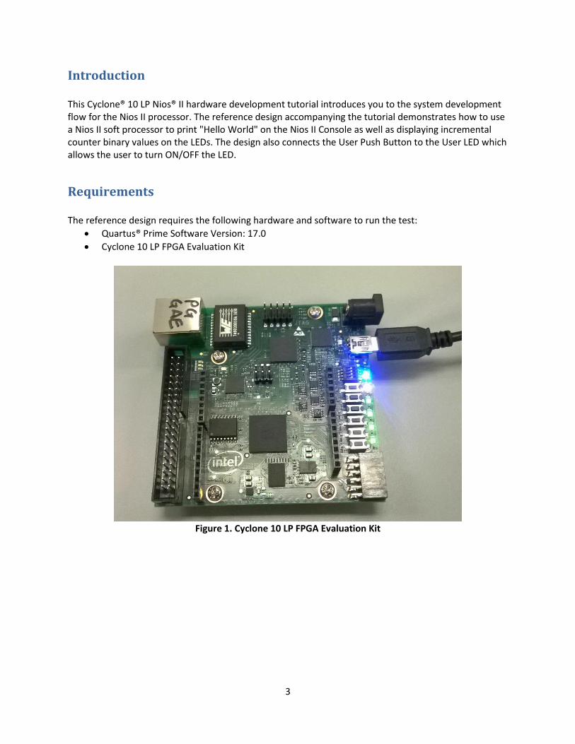
This Cyclone® 10 LP Nios® II hardware development tutorial introduces you to the system development flow for the Nios II processor. The reference design accompanying the tutorial demonstrates how to use a Nios II soft processor to print "Hello World" on the Nios II Console as well as displaying incremental counter binary values on the LEDs. The design also connects the User Push Button to the User LED which allows the user to turn ON/OFF the LED.
Requirements The reference design requires the following hardware and software to run the test:
• Quartus® Prime Software Version: 17.0
• Cyclone 10 LP FPGA Evaluation Kit
Figure 1. Cyclone 10 LP FPGA Evaluation Kit
4
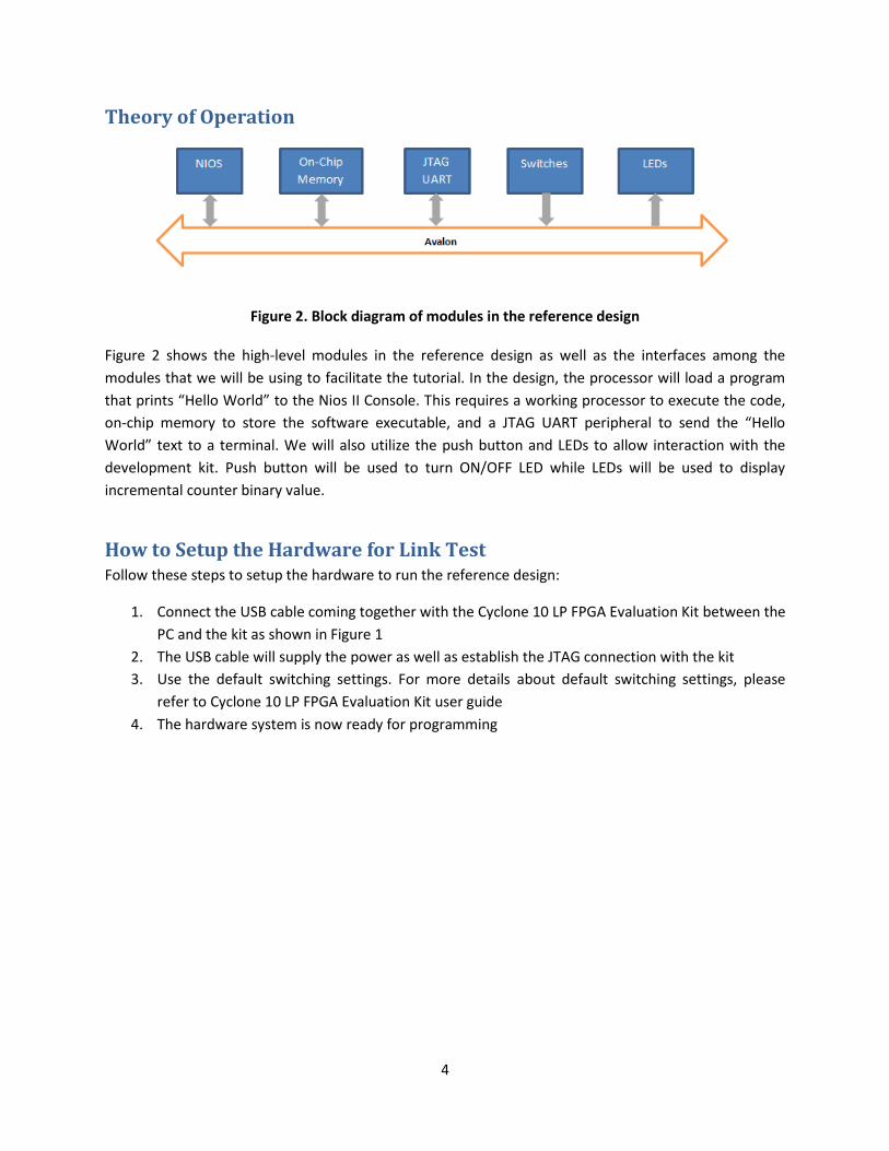
Theory of Operation
Figure 2. Block diagram of modules in the reference design
Figure 2 shows the high-level modules in the reference design as well as the interfaces among the
modules that we will be using to facilitate the tutorial. In the design, the processor will load a program
that prints “Hello World” to the Nios II Console. This requires a working processor to execute the code,
on-chip memory to store the software executable, and a JTAG UART peripheral to send the “Hello
World” text to a terminal. We will also utilize the push button and LEDs to allow interaction with the
development kit. Push button will be used to turn ON/OFF LED while LEDs will be used to display
incremental counter binary value.
How to Setup the Hardware for Link Test Follow these steps to setup the hardware to run the reference design:
1. Connect the USB cable coming together with the Cyclone 10 LP FPGA Evaluation Kit between the
PC and the kit as shown in Figure 1
2. The USB cable will supply the power as well as establish the JTAG connection with the kit
3. Use the default switching settings. For more details about default switching settings, please
refer to Cyclone 10 LP FPGA Evaluation Kit user guide
4. The hardware system is now ready for programming

5
How to Reconstruct and Running the Reference Design
Get Started with Quartus Download the reference design from Design Store and then follow the instruction in the Design Store to
prepare the design template and load the design into your Quartus software.
Building Your Qsys Based Processor System Now we can move on to build the Qsys system.
Launch Qsys from Quartus -> Tools -> Qsys. The initial screen is as shown in Figure 3.
Figure 3. Qsys Main Panel
Next, we will add various components of the system and make the connections between them. By
default, Qsys inserts a clock module. We will keep this and connect this later in the tutorial.
Below the IP catalog tab on the left, you can search for the various components you want to add to your
Qsys based system. Enter Nios in the search tab and select the “Nios II Processor” from the library.
Double Click on the name or click “Add”.
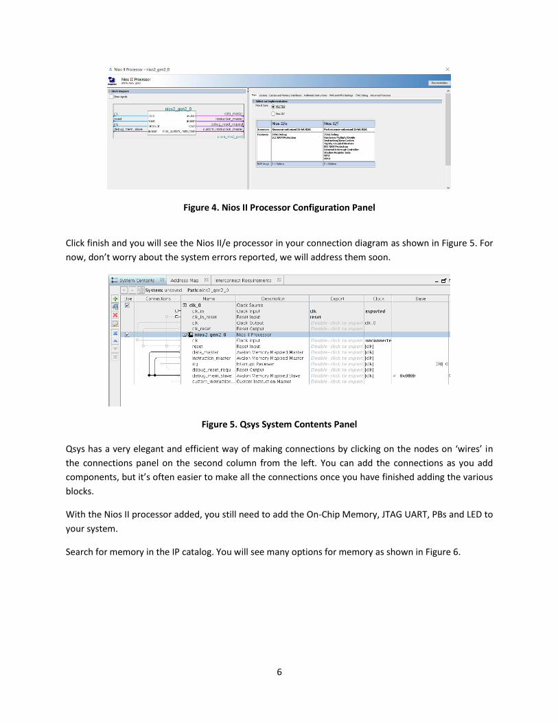
A configuration window will appear and select the “Nios II/e” as shown in Figure 4. This version of the
Nios II processor is resource optimized and will work well for this tutorial implementation.
6
Figure 4. Nios II Processor Configuration Panel
Click finish and you will see the Nios II/e processor in your connection diagram as shown in Figure 5. For
now, don’t worry about the system errors reported, we will address them soon.
Figure 5. Qsys System Contents Panel
Qsys has a very elegant and efficient way of making connections by clicking on the nodes on ‘wires’ in
the connections panel on the second column from the left. You can add the connections as you add
components, but it’s often easier to make all the connections once you have finished adding the various
blocks.
With the Nios II processor added, you still need to add the On-Chip Memory, JTAG UART, PBs and LED to
your system.
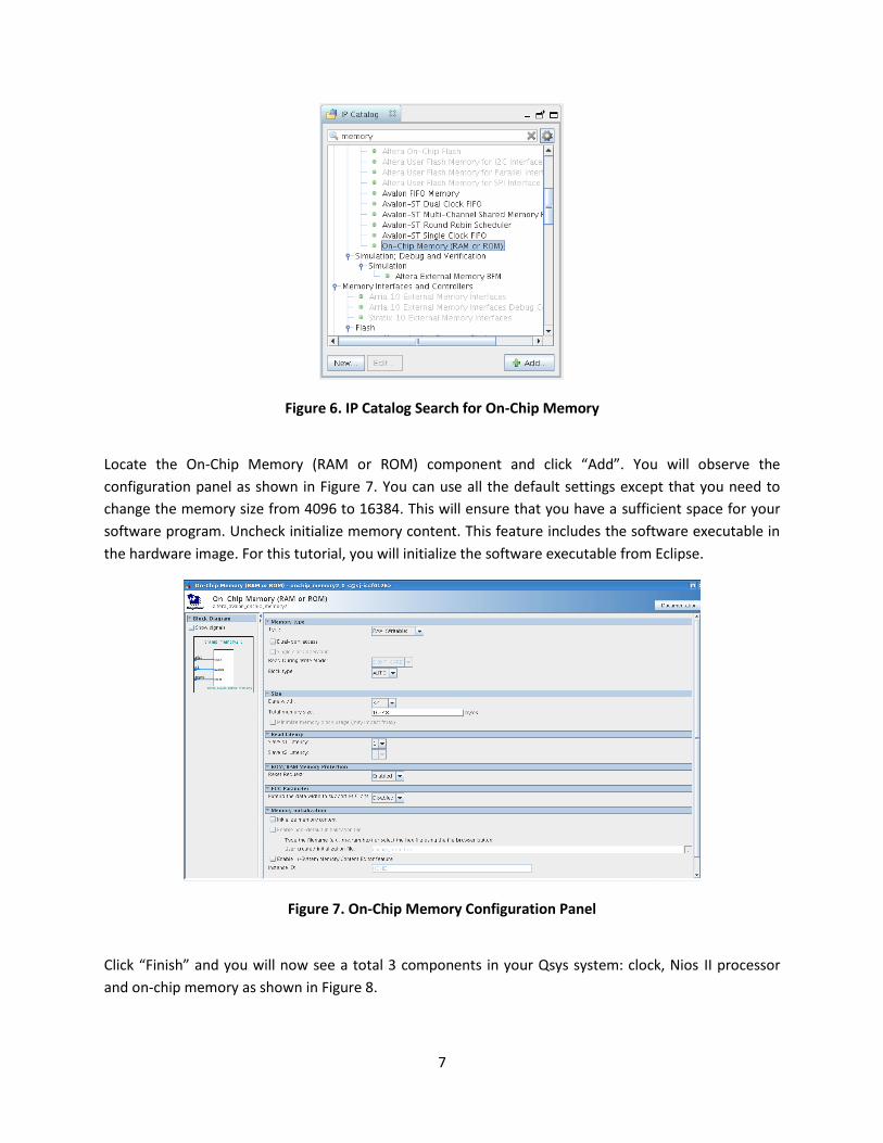
Search for memory in the IP catalog. You will see many options for memory as shown in Figure 6.
7
Figure 6. IP Catalog Search for On-Chip Memory
Locate the On-Chip Memory (RAM or ROM) component and click “Add”. You will observe the
configuration panel as shown in Figure 7. You can use all the default settings except that you need to
change the memory size from 4096 to 16384. This will ensure that you have a sufficient space for your
software program. Uncheck initialize memory content. This feature includes the software executable in
the hardware image. For this tutorial, you will initialize the software executable from Eclipse.
Figure 7. On-Chip Memory Configuration Panel
Click “Finish” and you will now see a total 3 components in your Qsys system: clock, Nios II processor
and on-chip memory as shown in Figure 8.
8
Figure 8. System Contents with Nios II and On-Chip Memory
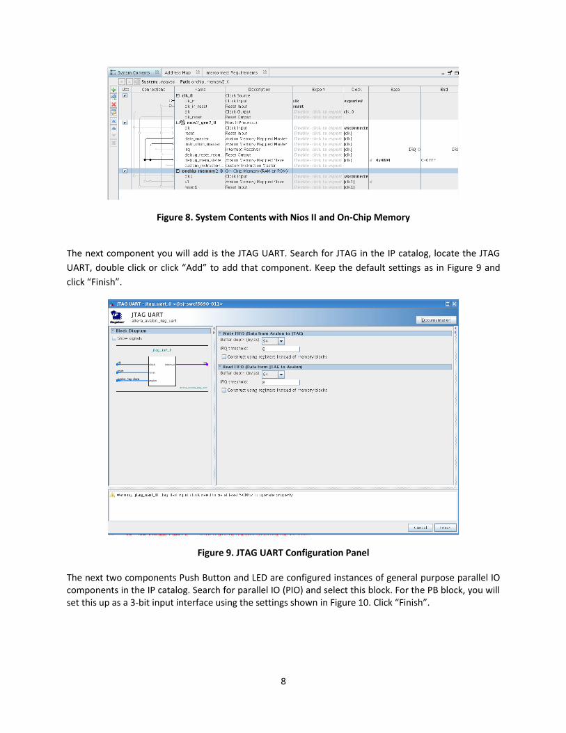
The next component you will add is the JTAG UART. Search for JTAG in the IP catalog, locate the JTAG
UART, double click or click “Add” to add that component. Keep the default settings as in Figure 9 and
click “Finish”.
Figure 9. JTAG UART Configuration Panel
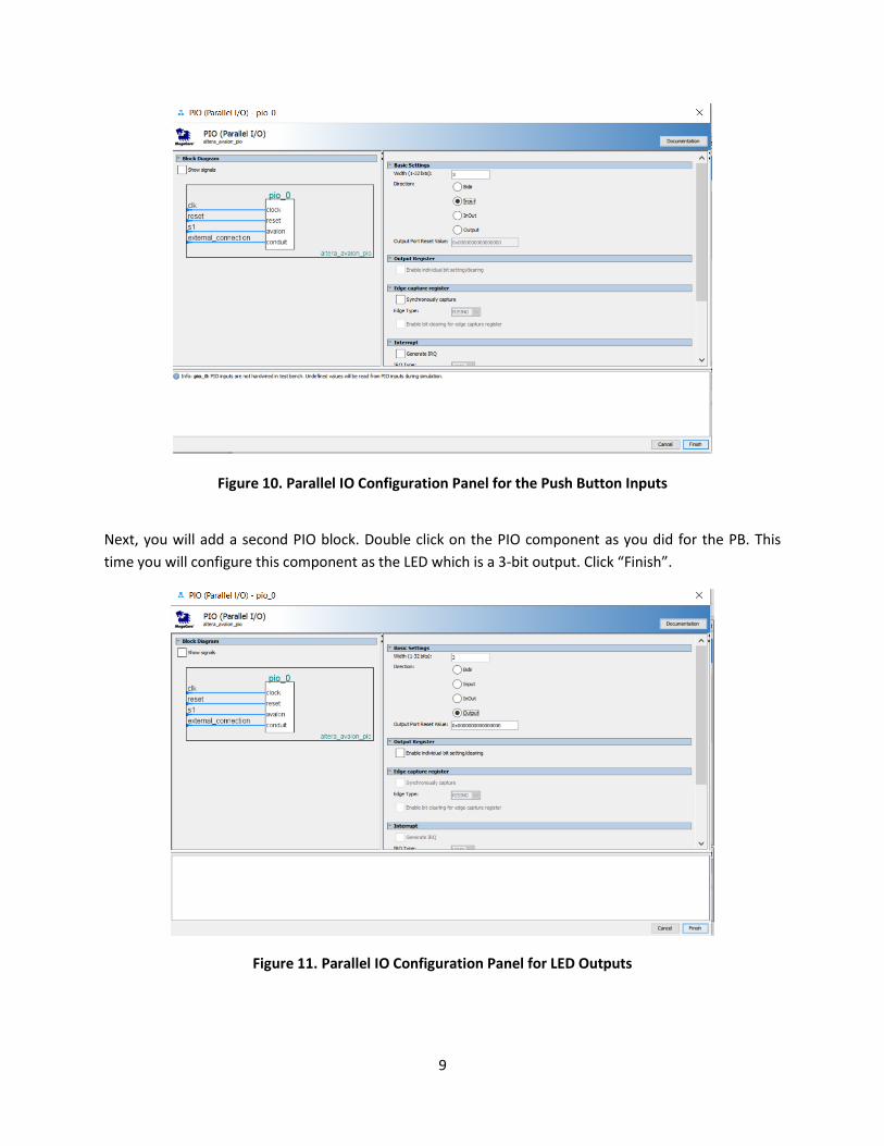
The next two components Push Button and LED are configured instances of general purpose parallel IO components in the IP catalog. Search for parallel IO (PIO) and select this block. For the PB block, you will set this up as a 3-bit input interface using the settings shown in Figure 10. Click “Finish”.
9
Figure 10. Parallel IO Configuration Panel for the Push Button Inputs
Next, you will add a second PIO block. Double click on the PIO component as you did for the PB. This
time you will configure this component as the LED which is a 3-bit output. Click “Finish”.
Figure 11. Parallel IO Configuration Panel for LED Outputs
10
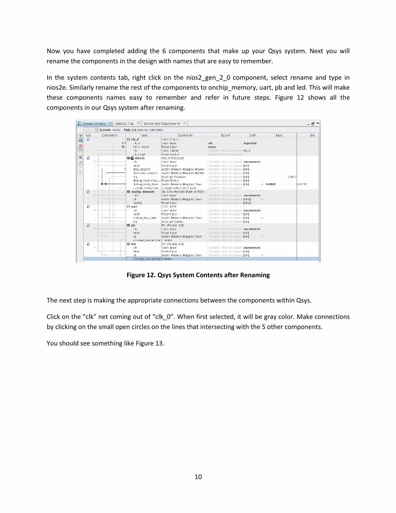
Now you have completed adding the 6 components that make up your Qsys system. Next you will
rename the components in the design with names that are easy to remember.
In the system contents tab, right click on the nios2_gen_2_0 component, select rename and type in
nios2e. Similarly rename the rest of the components to onchip_memory, uart, pb and led. This will make
these components names easy to remember and refer in future steps. Figure 12 shows all the
components in our Qsys system after renaming.
Figure 12. Qsys System Contents after Renaming
The next step is making the appropriate connections between the components within Qsys.
Click on the “clk” net coming out of “clk_0”. When first selected, it will be gray color. Make connections
by clicking on the small open circles on the lines that intersecting with the 5 other components.
You should see something like Figure 13.
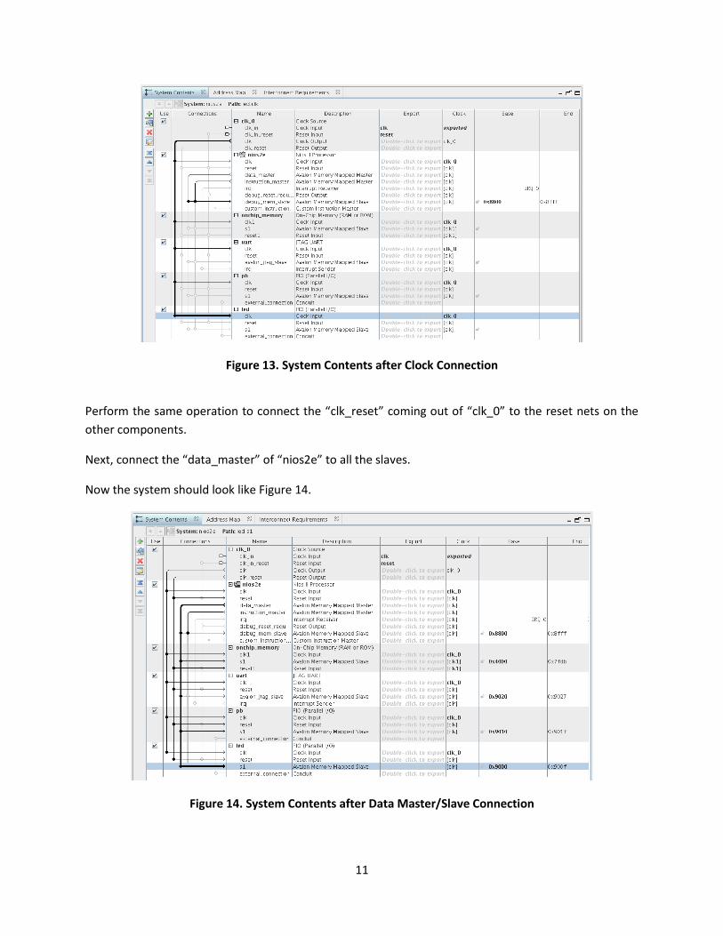
11
Figure 13. System Contents after Clock Connection
Perform the same operation to connect the “clk_reset” coming out of “clk_0” to the reset nets on the
other components.
Next, connect the “data_master” of “nios2e” to all the slaves.
Now the system should look like Figure 14.
Figure 14. System Contents after Data Master/Slave Connection
12
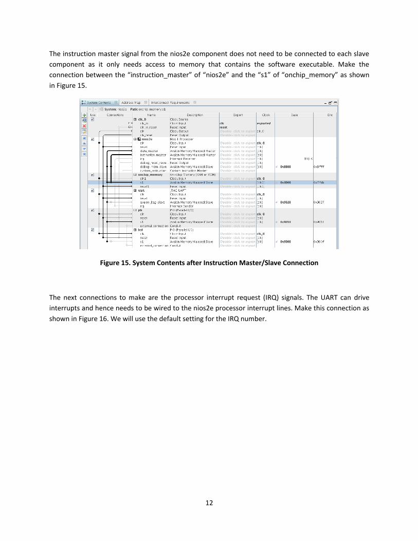
The instruction master signal from the nios2e component does not need to be connected to each slave
component as it only needs access to memory that contains the software executable. Make the
connection between the “instruction_master” of “nios2e” and the “s1” of “onchip_memory” as shown
in Figure 15.
Figure 15. System Contents after Instruction Master/Slave Connection
The next connections to make are the processor interrupt request (IRQ) signals. The UART can drive
interrupts and hence needs to be wired to the nios2e processor interrupt lines. Make this connection as
shown in Figure 16. We will use the default setting for the IRQ number.
13
Figure 16. System Contents after Interrupt Connections
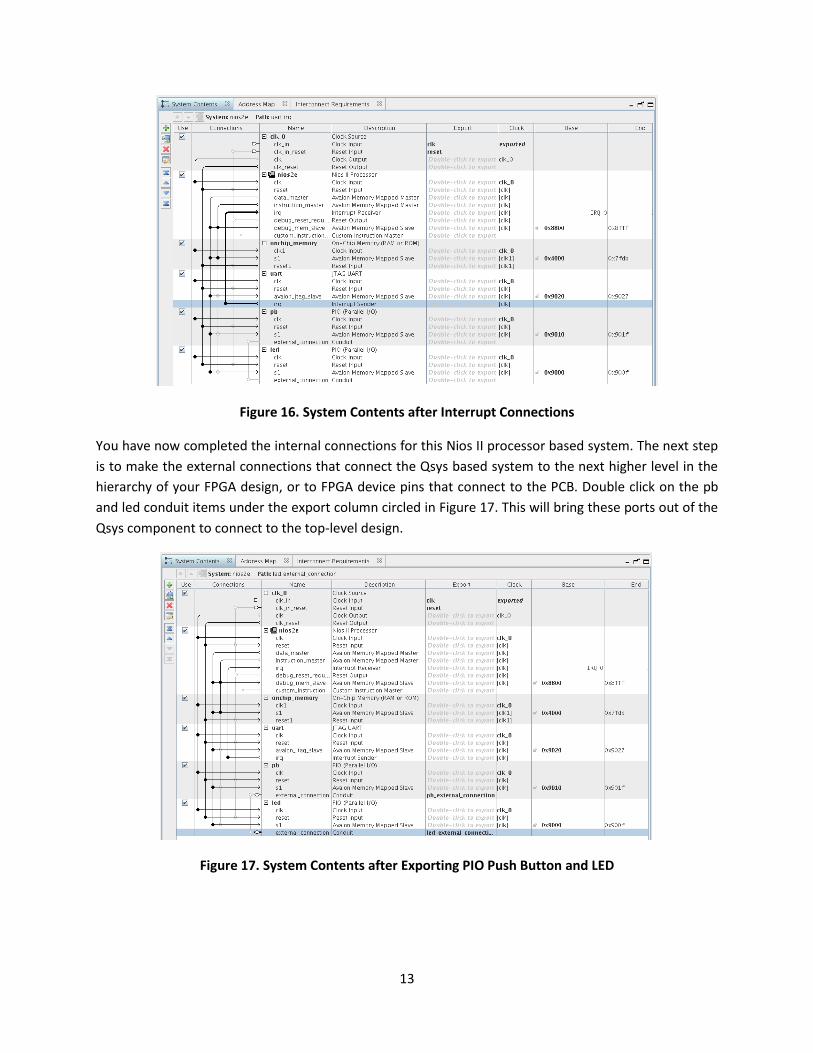
You have now completed the internal connections for this Nios II processor based system. The next step
is to make the external connections that connect the Qsys based system to the next higher level in the
hierarchy of your FPGA design, or to FPGA device pins that connect to the PCB. Double click on the pb
and led conduit items under the export column circled in Figure 17. This will bring these ports out of the
Qsys component to connect to the top-level design.
Figure 17. System Contents after Exporting PIO Push Button and LED

14
Next you will need to generate the base Addresses for your Qsys system. This is achieved by using the
command System -> Assign Base Addresses.
Save your Qsys system by using File -> Save As and pick a name for the Qsys system that you will
remember. Note that in the tutorial we call it “nios2e”. The information is saved in a. qsys file. Although
you are not finished, it’s always a good practice to save edits along the way.
You will see 2 error messages in the Message Console of Qsys, as shown in Figure 18.
Figure 18. Error Message Prior to Reset and Exception Specification
These error messages have something to do with the fact that nios2e processor doesn’t know where the
software code that handles resets and exceptions is located. This is straightforward to fix.
Double click on the nios2e component, Click tab “Vectors”. Set the “Reset Vector Memory” and
“Exception Vector Memory” both to “onchip_memory.s1”. This will set the system to execute from the
on-chip memory at these respective locations upon reset or interrupt. The 2 errors that were shown in
Figure 19 should now be resolved.
Figure 19. Assign Reset and Exception Vectors in the nios2e Panel
15
You may then save your design by clicking File -> Save and then generate the HDL files by clicking on the
button “Generate HDL” on the lower right of Qsys. Note that in this design, the nios2e.qsys has been
pre-created and the HDL files have been pre-generated. You may back up these pre-created files to a
folder for future reference or you may also directly use these files which have been verified working.
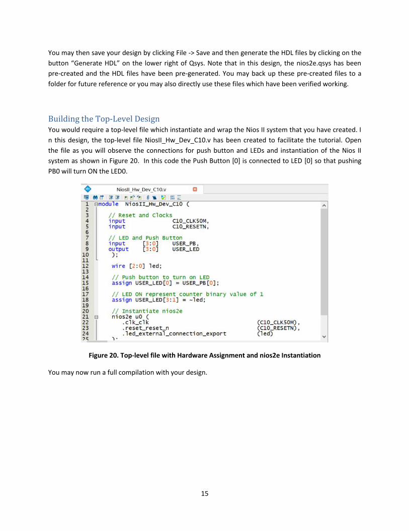
Building the Top-Level Design You would require a top-level file which instantiate and wrap the Nios II system that you have created. I
n this design, the top-level file NiosII_Hw_Dev_C10.v has been created to facilitate the tutorial. Open
the file as you will observe the connections for push button and LEDs and instantiation of the Nios II
system as shown in Figure 20. In this code the Push Button [0] is connected to LED [0] so that pushing
PB0 will turn ON the LED0.
Figure 20. Top-level file with Hardware Assignment and nios2e Instantiation
You may now run a full compilation with your design.
16
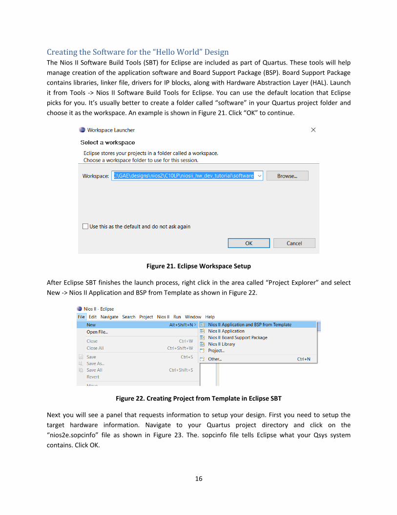
Creating the Software for the “Hello World” Design The Nios II Software Build Tools (SBT) for Eclipse are included as part of Quartus. These tools will help
manage creation of the application software and Board Support Package (BSP). Board Support Package
contains libraries, linker file, drivers for IP blocks, along with Hardware Abstraction Layer (HAL). Launch
it from Tools -> Nios II Software Build Tools for Eclipse. You can use the default location that Eclipse
picks for you. It’s usually better to create a folder called “software” in your Quartus project folder and
choose it as the workspace. An example is shown in Figure 21. Click “OK” to continue.
Figure 21. Eclipse Workspace Setup
After Eclipse SBT finishes the launch process, right click in the area called “Project Explorer” and select
New -> Nios II Application and BSP from Template as shown in Figure 22.
Figure 22. Creating Project from Template in Eclipse SBT
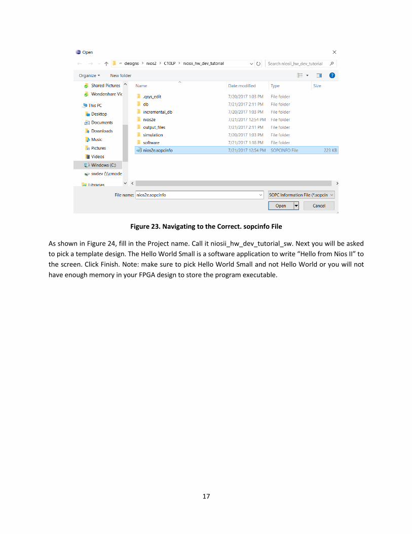
Next you will see a panel that requests information to setup your design. First you need to setup the
target hardware information. Navigate to your Quartus project directory and click on the
“nios2e.sopcinfo” file as shown in Figure 23. The. sopcinfo file tells Eclipse what your Qsys system
contains. Click OK.
17
Figure 23. Navigating to the Correct. sopcinfo File
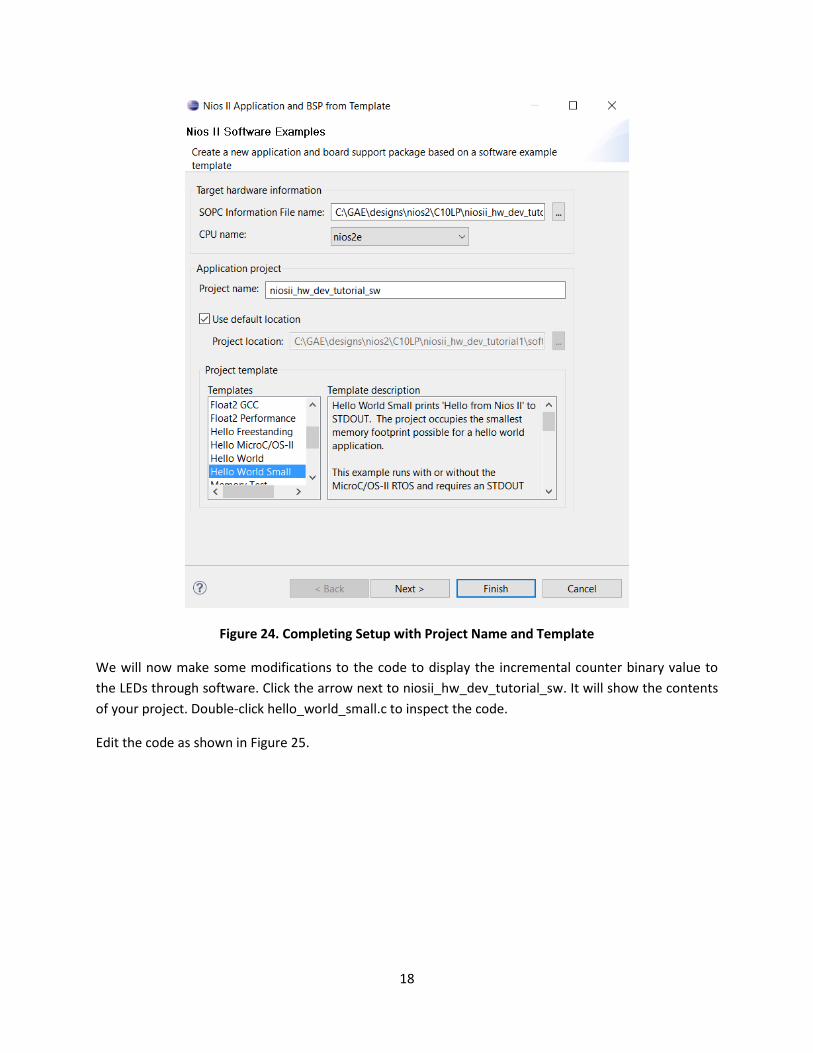
As shown in Figure 24, fill in the Project name. Call it niosii_hw_dev_tutorial_sw. Next you will be asked
to pick a template design. The Hello World Small is a software application to write “Hello from Nios II” to
the screen. Click Finish. Note: make sure to pick Hello World Small and not Hello World or you will not
have enough memory in your FPGA design to store the program executable.
18
Figure 24. Completing Setup with Project Name and Template
We will now make some modifications to the code to display the incremental counter binary value to
the LEDs through software. Click the arrow next to niosii_hw_dev_tutorial_sw. It will show the contents
of your project. Double-click hello_world_small.c to inspect the code.
Edit the code as shown in Figure 25.

19
Figure 25. Code Change in Eclipse SBT
You can copy the code from here:
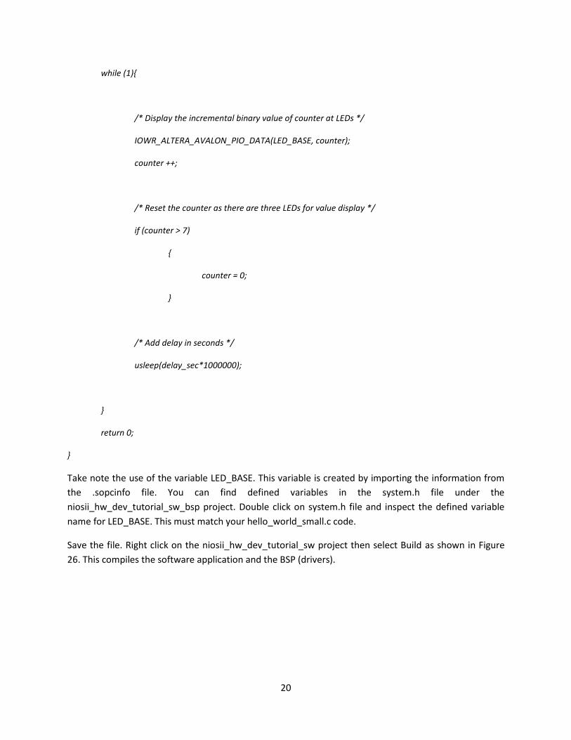
#include <sys/alt_stdio.h>
#include <stdio.h>
#include "altera_avalon_pio_regs.h"
#include "system.h"
#include <time.h>
int main()
{
/* Print in the Eclipse console */
alt_putstr("Hello World from Nios II!\n");
/* Initial parameters */
int counter = 0;
int delay_sec = 1;
/* Loop to display counter binary value */
20
while (1){
/* Display the incremental binary value of counter at LEDs */
IOWR_ALTERA_AVALON_PIO_DATA(LED_BASE, counter);
counter ++;
/* Reset the counter as there are three LEDs for value display */
if (counter > 7)
{
counter = 0;
}
/* Add delay in seconds */
usleep(delay_sec*1000000);
}
return 0;
}
Take note the use of the variable LED_BASE. This variable is created by importing the information from
the .sopcinfo file. You can find defined variables in the system.h file under the
niosii_hw_dev_tutorial_sw_bsp project. Double click on system.h file and inspect the defined variable
name for LED_BASE. This must match your hello_world_small.c code.
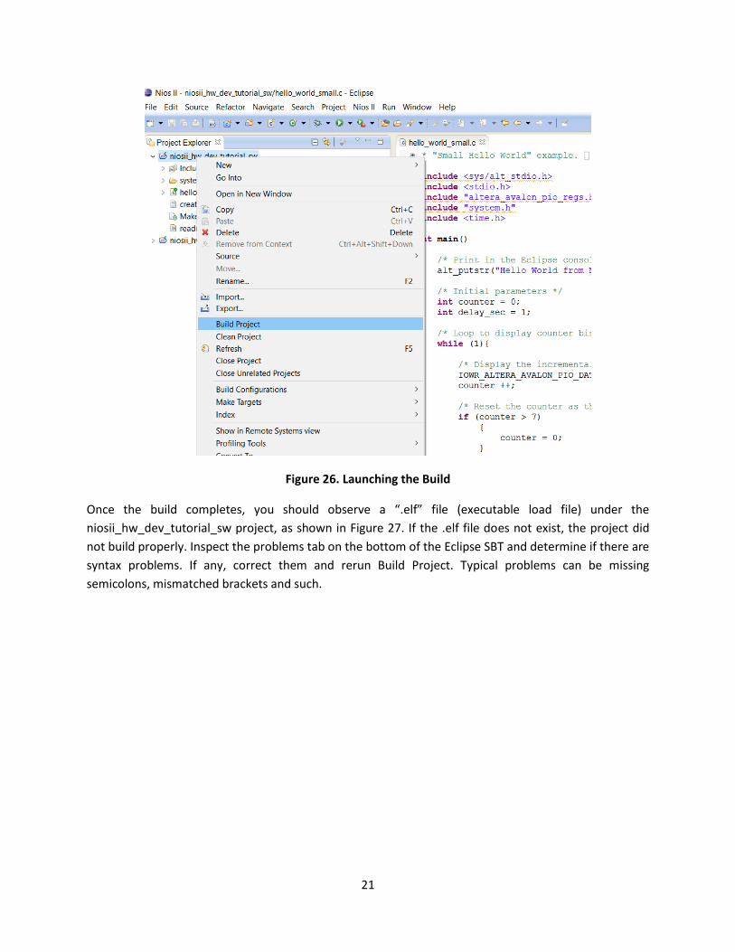
Save the file. Right click on the niosii_hw_dev_tutorial_sw project then select Build as shown in Figure
26. This compiles the software application and the BSP (drivers).
21
Figure 26. Launching the Build
Once the build completes, you should observe a “.elf” file (executable load file) under the
niosii_hw_dev_tutorial_sw project, as shown in Figure 27. If the .elf file does not exist, the project did
not build properly. Inspect the problems tab on the bottom of the Eclipse SBT and determine if there are
syntax problems. If any, correct them and rerun Build Project. Typical problems can be missing
semicolons, mismatched brackets and such.

22
Figure 27. niosii_hw_dev_tutorial_sw.elf Generated by Eclipse after Build Success

23
Downloading the Hardware Image The Cyclone 10 LP FPGA Evaluation Kit is powered through the USB cable. Connect the USB cable coming
together between the PC and the kit as shown in Figure 1. The kit should be powered up with LEDs on
the board light up. The USB cable will also establish the JTAG connection with the kit.
In Quartus II, launch the Programmer: Tools -> Programmer and then program the .sof into the kit. After
successful programming the kit, you can push PB0 to see if it can turn ON the LED0 as shown in Figure
28. If yes, it means that your hardware image was downloaded successfully.
Figure 28. Pushing of PB0 to turn ON LED0
24
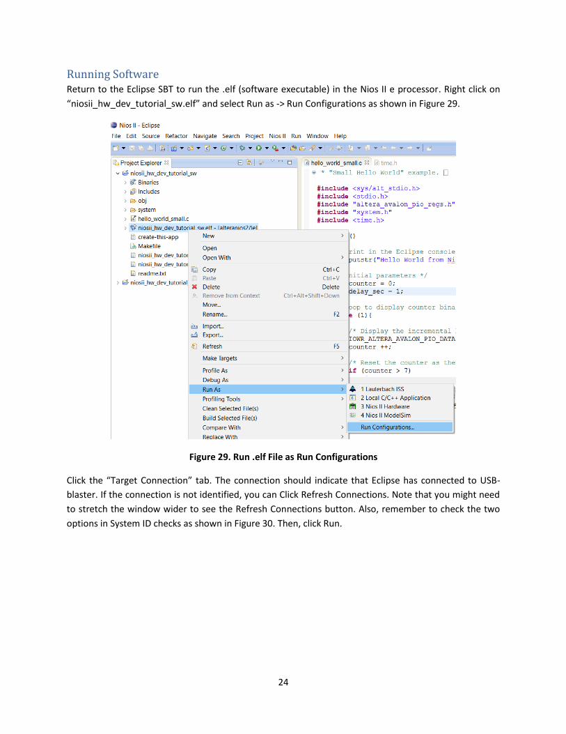
Running Software Return to the Eclipse SBT to run the .elf (software executable) in the Nios II e processor. Right click on
“niosii_hw_dev_tutorial_sw.elf” and select Run as -> Run Configurations as shown in Figure 29.
Figure 29. Run .elf File as Run Configurations
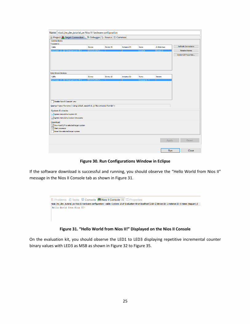
Click the “Target Connection” tab. The connection should indicate that Eclipse has connected to USB-
blaster. If the connection is not identified, you can Click Refresh Connections. Note that you might need
to stretch the window wider to see the Refresh Connections button. Also, remember to check the two
options in System ID checks as shown in Figure 30. Then, click Run.
25
Figure 30. Run Configurations Window in Eclipse
If the software download is successful and running, you should observe the “Hello World from Nios II”
message in the Nios II Console tab as shown in Figure 31.
Figure 31. “Hello World from Nios II!” Displayed on the Nios II Console
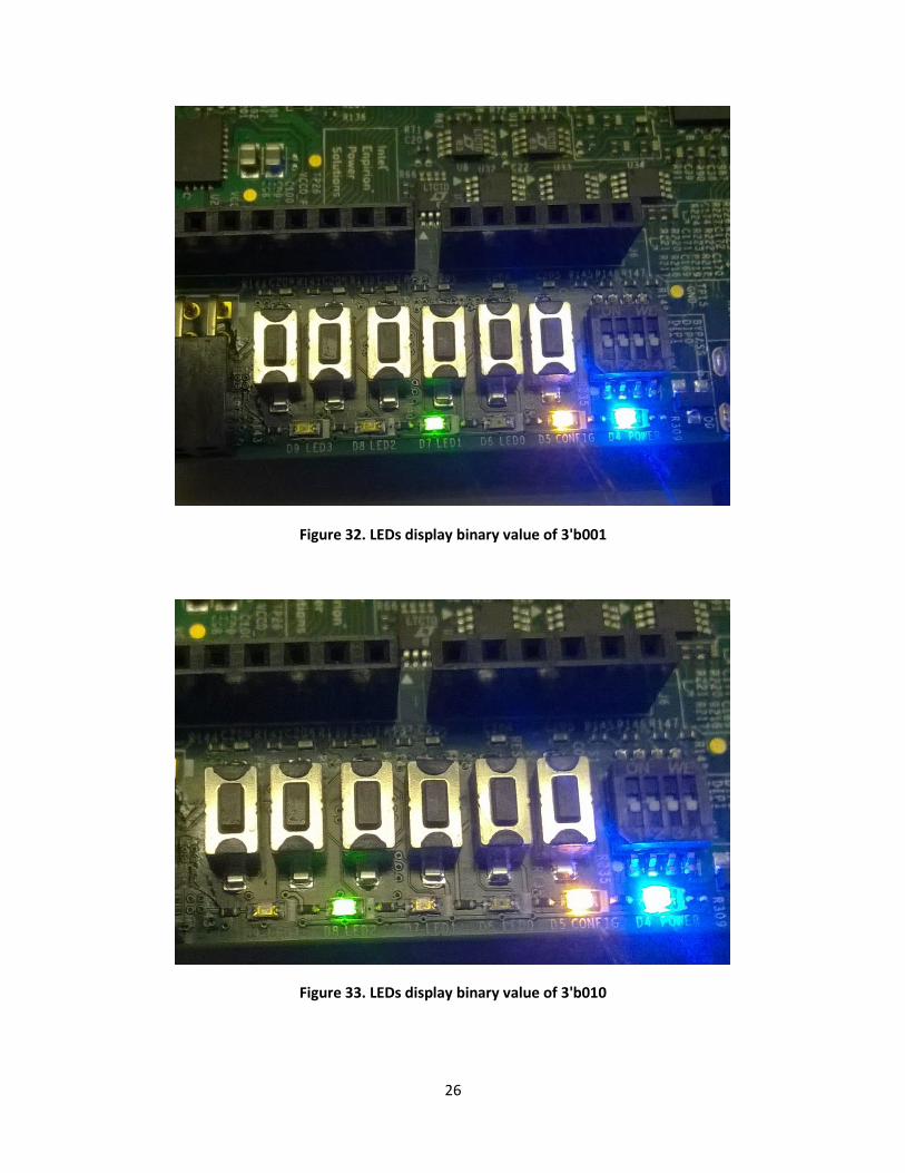
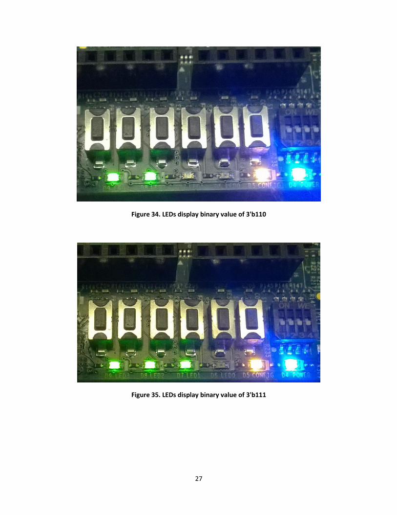
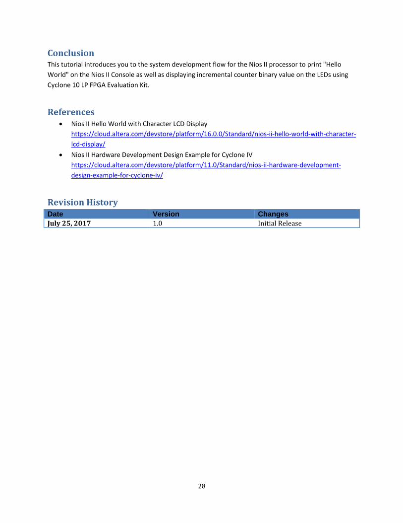
On the evaluation kit, you should observe the LED1 to LED3 displaying repetitive incremental counter
binary values with LED3 as MSB as shown in Figure 32 to Figure 35.
26
Figure 32. LEDs display binary value of 3'b001
Figure 33. LEDs display binary value of 3'b010
27
Figure 34. LEDs display binary value of 3'b110
Figure 35. LEDs display binary value of 3'b111
28
Conclusion This tutorial introduces you to the system development flow for the Nios II processor to print "Hello
World" on the Nios II Console as well as displaying incremental counter binary value on the LEDs using
Cyclone 10 LP FPGA Evaluation Kit.
References • Nios II Hello World with Character LCD Display
https://cloud.altera.com/devstore/platform/16.0.0/Standard/nios-ii-hello-world-with-character-
lcd-display/
• Nios II Hardware Development Design Example for Cyclone IV
https://cloud.altera.com/devstore/platform/11.0/Standard/nios-ii-hardware-development-
design-example-for-cyclone-iv/
Revision History Date Version Changes
July 25, 2017 1.0 Initial Release