Nios II Embedded Evaluation Kit, Cyclone III Edition User ... · 101 Innovation Drive San Jose, CA...
80
101 Innovation Drive San Jose, CA 95134 www.altera.com Nios II Embedded Evaluation Kit, Cyclone III Edition User Guide Document Date: July 2010 P25-36209-03
Transcript of Nios II Embedded Evaluation Kit, Cyclone III Edition User ... · 101 Innovation Drive San Jose, CA...

Nios II Embedded Evaluation Kit,Cyclone III Edition
101 Innovation DriveSan Jose, CA 95134www.altera.com
User Guide
Document Date: July 2010P25-36209-03

© 2010 Altera Corporation. All rights reserved. ALTERA, ARRIA, CYCLONE, HARDCOPY, MAX, MEGACORE, NIOS, QUARTUS and STRATIX areReg. U.S. Pat. & Tm. Off. and/or trademarks of Altera Corporation in the U.S. and other countries. All other trademarks and service marks are theproperty of their respective holders as described at www.altera.com/common/legal.html. Altera warrants performance of its semiconductor productsto current specifications in accordance with Altera's standard warranty, but reserves the right to make changes to any products and services at anytime without notice. Altera assumes no responsibility or liability arising out of the application or use of any information, product, or service describedherein except as expressly agreed to in writing by Altera. Altera customers are advised to obtain the latest version of device speci-fications before relying on any published information and before placing orders for products or services.
ii Development Board Version 1.0.0 Altera CorporationNios II Embedded Evaluation Kit, Cyclone III Edition User Guide July 2010
Part Number UG-01025-1.2

Altera Corporation July 2010
Contents
Chapter 1. Getting StartedIntroduction ............................................................................................................................................ 1–1Kit Contents ............................................................................................................................................ 1–2
About the Nios II Processor ............................................................................................................ 1–3About the Nios II Standard Design ............................................................................................... 1–3
About this User Guide .......................................................................................................................... 1–6Before You Begin .............................................................................................................................. 1–7
Software Installation ............................................................................................................................. 1–7Installing the Nios II Embedded Evaluation Kit, Cyclone III Edition ...................................... 1–7Installing the Quartus II Web Edition Software .......................................................................... 1–9Licensing the IP .............................................................................................................................. 1–11Licensing the EL Camino SD Card Core ..................................................................................... 1–13
Chapter 2. Development Board SetupFeatures ................................................................................................................................................... 2–1Requirements ......................................................................................................................................... 2–2Power Up the Development Board ..................................................................................................... 2–2
Chapter 3. Nios II Processor SystemsWhere to find the Nios II Processor Systems ..................................................................................... 3–3
Nios II 3C25 Standard Processor System ...................................................................................... 3–3Nios II 3C25 Video Processor System ........................................................................................... 3–4
Chapter 4. Application Selector UtilityOverview ................................................................................................................................................. 4–1
Ready-to-Run SD Card Demonstrations ....................................................................................... 4–1Running the Application Selector ....................................................................................................... 4–1
In system Update using SD Card ................................................................................................... 4–2Remote System Update using Ethernet .............................................................................................. 4–3
About Remote System Update ....................................................................................................... 4–3Requirements .................................................................................................................................... 4–4Operating Instructions ..................................................................................................................... 4–4
Creating Flash files for Remote System update ................................................................................ 4–6
Chapter 5. Design ExamplesAbout Design Examples ....................................................................................................................... 5–1Picture Viewer Application .................................................................................................................. 5–1
Picture Viewer .................................................................................................................................. 5–1Operation ........................................................................................................................................... 5–2
Mandelbrot Application ....................................................................................................................... 5–6
iiiPreliminary

Contents Contents
Using the Mandelbrot application ................................................................................................. 5–7Operation ......................................................................................................................................... 5–11
Application Selector ............................................................................................................................ 5–13About the Embedded Web Server ............................................................................................... 5–14
Appendix A. Video Pipeline Data FlowIntroduction ........................................................................................................................................... A–1Get the full LCD controller Application Note .................................................................................. A–2Creating a new 5:6:5 Pixel-Format component ................................................................................ A–2
Appendix B. Application Selector DetailsSD Card .................................................................................................................................................. B–1Application Files ................................................................................................................................... B–1SD Card Directory Structure ............................................................................................................... B–1CFI Flash ................................................................................................................................................ B–2
Hardware images ............................................................................................................................ B–2Software Images .............................................................................................................................. B–2Application Boot Code ................................................................................................................... B–3Flash Hardware Image Catalog .................................................................................................... B–3
Hardware Image Caching ................................................................................................................... B–4Flash Hardware Image Catalog .......................................................................................................... B–5Creating Your Own Loadable Applications ..................................................................................... B–6Rebuilding the Application Selector .................................................................................................. B–7
Create a BSP ..................................................................................................................................... B–8Build the project ............................................................................................................................... B–8Build the boot code ......................................................................................................................... B–9
Modifying the Application Selector ................................................................................................... B–9Changing the CFI flash map .......................................................................................................... B–9
Appendix C. Restoring the Factory ImageRestoring the Original Flash Image (Application Selector) ............................................................ C–1Rebuilding the Application Selector from Source Files .................................................................. C–2Boot Code ............................................................................................................................................... C–2Hardware Image Catalog .................................................................................................................... C–3Application Selector Hardware Image .............................................................................................. C–3Application Selector Software Image ................................................................................................ C–4Combining factory recovery image files ........................................................................................... C–4
Appendix D. Frequently Asked QuestionsWhy is my SOF time-limited? ....................................................................................................... D–1What are Ready-to-Run Demonstrations? ................................................................................... D–1Where can I find Ready-to-Run Demonstrations? ..................................................................... D–1What is in a ready-to-run demonstration ? ................................................................................. D–2How do ready-to-run demonstrations get loaded from the SD card to the FPGA? .............. D–2Where can I get more ready-to-run demonstrations? ................................................................ D–2Where can I get full Quartus II projects and source code for ready-to-run demonstrations? .............................................................................................................................. D–2
Altera Corporation ivJuly 2010 Preliminary

Contents
Why do I get the error “Can't find valid feature line for core SD_MMC_SPI_CORE (EC11_0002) in current license;Error: Error (10003): Can't open encrypted VHDL or Verilog HDL file” when I try to re-generate the Nios II Standard hardware design? .............................................................. D–3Where can I get the SD-Card Controller IP License? ................................................................. D–3How do I add pictures so the Picture Viewer Application can find them? ............................ D–3How do I add my own design so the Application Selector can find and run it? ................... D–4Where do I go to get more designs for the Nios II Embedded Evaluation Kit? ..................... D–4How do I open a design example in the Nios II IDE? ................................................................ D–4How do I restore the factory image? ............................................................................................ D–5How do I re-build the factory image? .......................................................................................... D–5
Additional InformationFurther Information .............................................................................................................................. i–ii
v Altera CorporationPreliminary July 2010

Contents Contents
Altera Corporation viJuly 2010 Preliminary

Altera Corporation DeveloJuly 2010
1. Getting Started
Introduction The Altera® Nios® II Embedded Evaluation Kit, Cyclone® III Edition includes a full-featured FPGA development board, LCD Multimedia High Speed Mezzanine Card (HSMC), hardware and software development tools, documentation, and accessories needed to begin embedded and system on a programmable chip (SOPC) designs using FPGAs.
The development board includes an Altera Cyclone III FPGA and comes preconfigured with an FPGA hardware reference design stored in flash memory as well as several ready-to-run demonstration applications stored on the SD-Card Flash provided. Hardware designers can use the FPGA reference design as a platform to build complex embedded systems. Software developers can use the hardware reference design plus sample software applications as a starting point for their own applications.
Success for an embedded system start rights from the evaluation stage. Choosing the right platform, development tools, operating systems may be the difference between success and failure. The Altera Nios II Embedded Evaluation Kit, Cyclone III Edition is an evaluation kit that enables you to make these critical decisions with minimal investment.
The Nios II Embedded Evaluation Kit, Cyclone III Edition makes evaluating Altera’s embedded solutions easy. Processor systems targeting the low-cost, low-power Cyclone III FPGA can be evaluated by simply using the LCD Color Touch Panel to scroll through and load your demonstration of choice.
These processor systems showcase the unique benefits of FPGA-based processors such as reducing BOM costs by integrating powerful graphics engines within the FPGA, reducing operating costs by upgrading your system over the Internet, or increasing system performance while reducing power using C-to-Hardware (C2H) acceleration.
pment Board Version 1.0. 1–1Preliminary
Getting Started
Kit Contents The Nios II Embedded Evaluation kit will acquainting you with the Nios II processor, the hardware and software development flows and the robust embedded ecosystem of operating systems, middleware, IP and third party offerings that support the Nios II processor.
To this end the kit features:
■ Pre-built embedded processor systems that serve as starting points to accelerate hardware development
● Nios II Standard Processor System (Standard)● Nios II Video Based Embedded Processor System (Video)
■ Pre-built embedded applications with source code to serve as examples for software device driver development
● Altera Application Selector with embedded Web Server● Altera Picture Viewer● Altera Mandelbrot
■ Hardware and Software Tutorials to learn the embedded development flows
● My first FPGA design● My first Nios II Software tutorial
■ Ready-to-Run Demonstration applications from Altera’s partners
● IP: SD Card Controller (El Camino) , Graphics Engines (TES, Imagem, PlanetWeb)
● Operating systems: MicroC-OS II (Micrium Evaluation Licenses) , uC-Linux (SLS)
● Middleware: Filesystems (El Camino, Micrium, SLS), Graphics Libraries (Micrium)
■ Altera Evaluation IP license cores and software packages for embedded development
● Nios II IP Core (Evaluation Core)● DDR SDRAM Memory IP Core (Evaluation Core)● TSE MAC IP Core (Evaluation Core)● NicheStack TCP-IP Network Stack, Nios II Edition (Evaluation
Core)
Altera Corporation Development Board Version 1.0. 1–2July 2010 Nios II Embedded Evaluation Kit, Cyclone III Edition

Kit Contents
About the Nios II Processor
Nios II is a fully configurable 32-bit processor optimized for use in Altera’s FPGA. The embedded processor system is easily customized for a particular application using the SOPC Builder feature of the Quartus II FPGA design software.
Assembling a microprocessor system involves four elements:
1. Adding and configuring of the core processor and memory
2. Adding peripherals such as memory interfaces, I/O, or interfaces to external devices (such as the LCD Display)
3. Connecting the I/O pins of the processor in the FPGA to the external devices
4. Writing C/C++ software application for your custom processor with the Nios II Embedded Design Suite.
In the vast majority of cases, hardware design can be accomplished using drop-down menus and drag and drop operations in SOPC Builder. The sophistication of Altera's designs tools brings creating custom hardware processor systems within the reach of embedded developers.
About the Nios II Standard Design
The starter reference design for the board entitled “standard” is located in the altera\<version #>\kits\ cycloneIII_3c25_niosII\examples folder. The Nios II “standard” is a SOPC Builder system featuring the Nios II processor and common peripherals that has been put together for you. Hardware designers can accelerate their SOPC Builder system development by using the Nios II Standard design example as a starting point. The board boots up with this pre-built design, so software developers can use it for software development without having to concern themselves with the details of generating the FPGA hardware system.
The Nios II Standard System is a pre-generated hardware system that includes:
■ Nios II core (32-bit soft processor) Application
■ LCD Controller
■ Multi-port memory controllers
1–3 Development Board Version 1.0. Altera CorporationNios II Embedded Evaluation Kit, Cyclone III Edition July 2010

Getting Started
■ Communication Interface controllers
About the Nios II System Designs
A Nios II system design builds upon a Nios II processor system by including a software application that runs on the processor system.
Software developers can use system designs to see examples of software drivers for the hardware peripherals. Nios II Embedded Evaluation kit contains several system design examples:
■ Altera Application Selector■ Altera Picture Viewer■ Altera Mandelbrot C2H
1 Designs are located in the altera\<version #>\kits\cycloneIII_3c25_niosII in either the examples or demonstrations directory. You can also find more system designs from the Nios II Embedded Evaluation Kit (NEEK), Cyclone III Edition page.
About the Demonstrations
In the Nios II I Embedded Evaluation Kit directory, there is a demos folder (refer to Figure 1–1 on page 1–8). This is a repository of pre-built example Nios II based processor systems that have been provided for demonstration and evaluation purposes only.
How are the demonstrations different from design examples?
Design examples (located in the <Install Dir>\examples folder) are prebuilt processor systems that can be used as a starting point for your design.
1. Hardware Design Examples: Quartus II projects with pre-generated SOPC Builder systems featuring the Nios II processor (for example, standard)
2. System Design Examples: These build upon hardware design examples and include applications and source codes that show examples of software device drivers, operating system usage, and application selector.
Demonstrations (located in <Install Dir>\demos directory) are pregenerated SOPC Builder systems for evaluation purposes only and are not guaranteed to be updated with each release of the Quartus II software. When source-code is provided, recompiling a demonstration application from this directory may or may not work with the Quartus II
Altera Corporation Development Board Version 1.0. 1–4July 2010 Nios II Embedded Evaluation Kit, Cyclone III Edition

Kit Contents
version that was pointed to by the development kit documentation. Any source-code provided should be viewed as diagramatic but not necessarily functional.
Ready-to-run demonstrations are binaries that provide a quick and easy way to demonstrate and evaluate operating systems, middleware, IP and software tools for your Nios II processor system. These demonstrations are easily selected and loaded using the application selector on your LCD touch panel. These demonstrations are implementations of applications such as automotive graphics, consumer GUI, industrial control that are provided for demonstration and evaluation purposes by Altera and third party vendors.
If you want to select a suitable operating system (for example, Micriums uC-OS II or SLS's port of uC-Linux for Nios II), a particular IP core (for example, SD Card core or high performance vector graphics engine), middleware libraries (for example, Networks Stacks, Graphics Library) or graphics development tools (for example, PlanetWeb SpectraWorks, Altia Design), then the ready-to-run demonstrations help you make your evaluation process easy.
Ready-to-run demonstrations are provided in binary format only (.flash), full Quartus II projects, source code, and IP licensing and can be obtained by contacting the provider of the ready-to-run demonstrations. You can locate these demonstrations on your SD Card. Alternatively, you can download the latest ready-to-run demonstrations from the Nios II Embedded Evaluation Kit (NEEK), Cyclone III Edition page.
To add ready-to-run demonstrations to your SD Card, download the demonstration and copy it to your SD Card in the Altera_EEK_applications folder.
Table 1–1 list ready-to-run demonstration applications.
Table 1–1. List of Example Applications (Part 1 of 2)
Demonstration Vendor
Application Selector/Web Server Altera
Altera Picture Viewer Altera
Altera Mandelbrot C2H Altera
Altera Spinning Cube Altera
Imagem Tacquin Game Imagem
Imagem Watch Imagem
Imagem Avionics Imagem
1–5 Development Board Version 1.0. Altera CorporationNios II Embedded Evaluation Kit, Cyclone III Edition July 2010

Getting Started
About this User Guide
This user guide describes how to start using the Altera Nios II Embedded Evaluation Kit, including unpacking the kit, installing required software, and running the Application Selector utility and other design examples. This user guide addresses the following topics:
■ How to set up, power up, and verify correct operation of the Nios II Embedded Evaluation board
■ Nios II standard processor system for the Embedded Evaluation board
■ How to install the Nios II Embedded Evaluation Kit, Cyclone III Edition
■ How to install the Altera Quartus II Web Edition software ■ How to start and run the Application selector utility■ Design examples■ Taking the next step■ Frequently asked questions
f For a full description of the development boards and their design and use, refer to the Cyclone III FPGA Starter Board Reference Manual and LCD Multimedia HSMC Reference Manual.
This user guide provides an overview of some of the applications. For more information about key hardware components and the structure of the application selector utility, refer to Appendix A, Video Pipeline Data Flow, Appendix B, Application Selector Details, Appendix C, Restoring
uC-GUI Demonstration Micrium
Photo Frame PlanetWeb PlanetWeb
SpectraWorks GUI Demonstration by PlanetWeb
PlanetWeb
DAVE 2D Graphics Demonstration TES
Altia Red HMI Altia
Altia Blue HMI Altia
Imagem aPhone Imagem
Imagem 2-D Demonstration Imagem
Imagem Instrumentation Imagem
SLS uClinux SLS
PlanetWeb Menu PlanetWeb
Table 1–1. List of Example Applications (Part 2 of 2)
Demonstration Vendor
Altera Corporation Development Board Version 1.0. 1–6July 2010 Nios II Embedded Evaluation Kit, Cyclone III Edition

Software Installation
the Factory Image, and Appendix D, Frequently Asked Questions. However, we opted to provide extensive source-code comments rather than formal documentation regarding the other applications.
1 We are interested in knowing if this structure for the documentation is adequate for you to be able to develop your applications. If you have comments or suggestions on what we can do to improve the user experience through our documentation, contact us through [email protected].
f To ensure that you have the most up-to-date information on this product, refer to the Nios II Embedded Evaluation Kit (NEEK), Cyclone III Edition page.
Before You Begin
Before proceeding, check the contents of the kit:
■ Nios II Embedded Evaluation Board■ Cables and accessories
Software Installation
This section describes the following procedures:
■ “Installing the Nios II Embedded Evaluation Kit, Cyclone III Edition”
■ “Installing the Quartus II Web Edition Software” on page 1–9■ “Licensing the IP” on page 1–11■ “Licensing the EL Camino SD Card Core” on page 1–13
Installing the Nios II Embedded Evaluation Kit, Cyclone III Edition
The license-free Nios II Embedded Evaluation Kit, Cyclone III Edition installer includes all the documentation and design examples for the kit.
To install the Nios II Embedded Evaluation Kit, Cyclone III Edition, follow these steps:
1. Download the Nios II Embedded Evaluation Kit, Cyclone III Edition installer from the Nios II Embedded Evaluation Kit (NEEK), Cyclone III Edition page of the Altera website. Alternatively, you can request a development kit DVD from the Development Kits, Daughter Cards & Programming Hardware page of the Altera website.
1–7 Development Board Version 1.0. Altera CorporationNios II Embedded Evaluation Kit, Cyclone III Edition July 2010

Getting Started
2. Follow the on-screen instructions to complete the installation process.
The installation program creates the Nios II Embedded Evaluation Kit, Cyclone III Edition directory structure shown in Figure 1–1.
Figure 1–1. Nios II I Embedded Evaluation Kit Installed Directory Structure
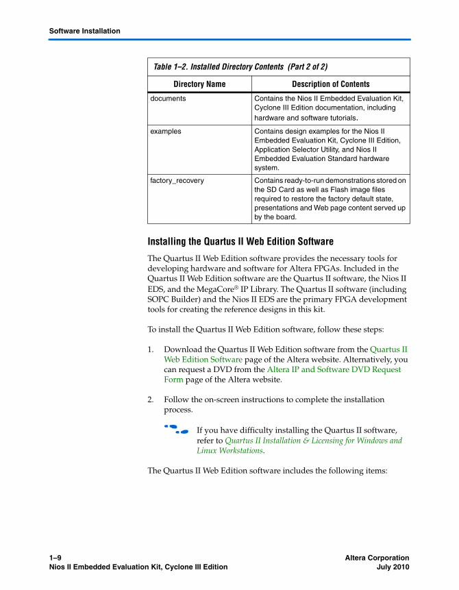
Table 1–2 lists the file directory names and a description of their contents.
Table 1–2. Installed Directory Contents (Part 1 of 2)
Directory Name Description of Contents
board_design_files Contains schematic, layout, assembly, and bill of material board design files.
demos Contains a repository of example designs that may be useful for demonstration or evaluation.
<install dir>
documents
board_design_files
The default Windows installation directory is C:\altera\<version>\.
examples
factory_recovery
demos
kits
cycloneIII_3c25_niosII
Altera Corporation Development Board Version 1.0. 1–8July 2010 Nios II Embedded Evaluation Kit, Cyclone III Edition
Software Installation
Installing the Quartus II Web Edition Software
The Quartus II Web Edition software provides the necessary tools for developing hardware and software for Altera FPGAs. Included in the Quartus II Web Edition software are the Quartus II software, the Nios II EDS, and the MegaCore® IP Library. The Quartus II software (including SOPC Builder) and the Nios II EDS are the primary FPGA development tools for creating the reference designs in this kit.
To install the Quartus II Web Edition software, follow these steps:
1. Download the Quartus II Web Edition software from the Quartus II Web Edition Software page of the Altera website. Alternatively, you can request a DVD from the Altera IP and Software DVD Request Form page of the Altera website.
2. Follow the on-screen instructions to complete the installation process.
f If you have difficulty installing the Quartus II software, refer to Quartus II Installation & Licensing for Windows and Linux Workstations.
The Quartus II Web Edition software includes the following items:
documents Contains the Nios II Embedded Evaluation Kit, Cyclone III Edition documentation, including hardware and software tutorials.
examples Contains design examples for the Nios II Embedded Evaluation Kit, Cyclone III Edition, Application Selector Utility, and Nios II Embedded Evaluation Standard hardware system.
factory_recovery Contains ready-to-run demonstrations stored on the SD Card as well as Flash image files required to restore the factory default state, presentations and Web page content served up by the board.
Table 1–2. Installed Directory Contents (Part 2 of 2)
Directory Name Description of Contents
1–9 Development Board Version 1.0. Altera CorporationNios II Embedded Evaluation Kit, Cyclone III Edition July 2010

Getting Started
■ The Quartus II software—The Quartus II software, including the SOPC Builder system development tool, provides a comprehensive environment for system-on-a-programmable-chip (SOPC) design. The Quartus II software integrates into nearly any design environment and provides interfaces to industry-standard EDA tools.
f To compare the Quartus II subscription and web editions, refer to Altera Quartus II Software—Subscription Edition vs. Web Edition. The kit also works with the subscription edition.
■ MegaCore IP Library—A library that contains Altera IP MegaCore functions. You can evaluate MegaCore functions with the OpenCore Plus feature to do the following tasks:
● Simulate behavior of a MegaCore function in your system● Verify functionality of your design, and quickly and easily
evaluate its size and speed● Generate time-limited device programming files for designs that
include MegaCore functions● Program a device and verify your design in hardware
1 The OpenCore Plus hardware evaluation feature is an evaluation tool for prototyping only. You must purchase a license to use a MegaCore function in production.
f For more information about OpenCore Plus, refer to AN 320: OpenCore Plus Evaluation of Megafunctions.
■ Nios II Embedded Design Suite (EDS)—A full-featured tool set that allows you to develop embedded software for the Nios II processor which you can include in your Altera FPGA designs.
Licensing Considerations
The Quartus II Web Edition software is license-free and supports Cyclone III devices without any additional licensing requirement. This kit also works with the Quartus II Subscription Edition software, after you obtain the proper license file. To purchase a subscription, contact your Altera sales representative.
Altera Corporation Development Board Version 1.0. 1–10July 2010 Nios II Embedded Evaluation Kit, Cyclone III Edition

Software Installation
Licensing the IP
After installing the Quartus II Web Edition software, you will have installed an OpenCore Plus evaluation of the Nios II IP core. Any designs you create operate in Altera’s OpenCore Plus evaluation mode and allow you to do the following:
1. Simulate the behavior of the Nios II processor IP in your system.
2. Verify the functionality of your design, as well as evaluate its size and speed quickly and easily.
3. Generate time-limited device programming files for designs that include a Nios II processor.
4. Program a device and verify your design in hardware.
OpenCore Plus hardware evaluation supports the following two modes of operation:
Tethered—requires a JTAG connection between your board and the host computer. If tethered mode is supported by all megafunctions in a design, the device can operate for a longer time or indefinitely.
Untethered—the design runs for a limited time.
To ship designs with the Nios II IP Core you need to obtain a license for the Nios II IP (IP-NIOS). To obtain a license you can:
1. Contact your local Altera representative at www.altera.com/corporate/contact/con-index.html
2. Use the Altera Tools Support at www.altera.com/corporate/contact/info/con-phone.html to order today.
Nios II Processor—To obtain a non-time-limited use license file for the Nios II processor, you must purchase a stand-alone Nios II processor core license (ordering code: IP-NIOS). Contact your local Altera representative or Altera Tools Support to order today.
Nios II C2H Compiler—You can create, compile, and generate time-limited Nios II processor systems and hardware accelerators generated by the Nios II C2H Compiler without obtaining a license file with the OpenCore Plus evaluation feature. You must obtain a license for the Nios II processor core (ordering code: IP-NIOS) and Nios II C2H Compiler (ordering code: IPT-C2H-NIOS) to generate non-time-limited
1–11 Development Board Version 1.0. Altera CorporationNios II Embedded Evaluation Kit, Cyclone III Edition July 2010

Getting Started
programming files and flash programming files. Contact your local Altera representative or use the Altera Tools Support to order today. You do not need a license if you are developing software with the Nios II IDE.
NicheStack TCP/IP Stack–Nios II Edition—You can develop software for any of the Nios II development kits using the NicheStack TCP/IP Stack, Nios II Edition evaluation. To generate software to run on other boards and/or ship in a product, you must obtain a license (ordering code: IPSW-TCP/IP-NIOS). Contact your local Altera representative or Altera Tools Support to order today.
Micrium MicroC/OS-II RTOS— You can develop software for any of the Nios II development kits using the Micrium MicroC/OS-II RTOS. To generate software to run on other boards, ship in a product, or both, you must obtain a license. To obtain a license for the Micrium MicroC/OS-II RTOS, contact Micrium today.
Altera IP Base Suite— A high performance memory controller for the on-board DDR SDRAM memory is available from Altera.
■ Finite Impulse Response (FIR) Compiler ■ Fast Fourier Transform (FFT) Compiler ■ Numerically Controlled Oscillator (NCO) Compiler ■ DDR SDRAM Controller ■ DDR SDRAM High-Performance Controller ■ DDR2 SDRAM Controller ■ DDR2 SDRAM High-Performance Controller ■ DDR3 SDRAM High-Performance Controller ■ QDRII SRAM Controller ■ RLDRAM II Controller ■ SerialLite II
To help shorten your design time, Altera provides some of its most popular intellectual property (IP) cores with the Altera IP Base Suite, which is completely free with a Quartus II subscription.
f For more information about obtaining the Altera IP Base Suite, refer to the Free IP Base Suite Licenses With Active Quartus II Subscription page.
Altera Corporation Development Board Version 1.0. 1–12July 2010 Nios II Embedded Evaluation Kit, Cyclone III Edition

Software Installation
Licensing the EL Camino SD Card Core
The Nios II Standard hardware design contains the SD MMC SPI CORE which is a component that has been provided by a third party vendor, El Camino. To compile this core in your SOPC Builder system, you must obtain a license from El Camino.
However, if your particular application has no need to access the SD Card then you do not need to include the SD Card core in your system. Simply uncheck this core or delete it and regenerate the system. You should now be able to rebuild the hardware system without error.
If your design requires access to the on-board SD Card then you can request an evaluation license or purchase the SD-Card Controller IP, drivers and FAT File system from El Camino.
El Camino GmbH Landshuter Str. 1D-84048 MainburgGermanyTel. +49 - 8751 - 8787 - 0Fax +49 - 8751 - 842876 Web: www.elcamino.de E-mail: [email protected]
1–13 Development Board Version 1.0. Altera CorporationNios II Embedded Evaluation Kit, Cyclone III Edition July 2010

Getting Started
Altera Corporation Development Board Version 1.0. 1–14July 2010 Nios II Embedded Evaluation Kit, Cyclone III Edition

Altera Corporation DeveloJuly 2010
2. Development Board Setup
Features The Nios II Embedded Evaluation Kit features:
■ Cyclone III Starter Board● Cyclone III EP3C25F324 FPGA● Configuration
• Embedded USB-Blaster™ circuitry (includes an Altera EPM3128A CPLD) allowing download of FPGA configuration files via the users USB port
● Power and analog devices from Linear Technology● Memory
• 256-Mbit DDR SDRAM• 1-Mbyte Synchronous SRAM• 16-Mbytes Intel P30/P33 flash
● Clocking• 50-MHz on-board oscillator
● Switches and indicators• Six push buttons total, 4 user controlled• Four user-controlled LEDs
■ LCD Daughtercard● LCD Touch-screen Display
• 800 X 480 pixel size● 10-bit VGA DAC● Video Decoder● 24-bit Audio Codec● RS232 transceiver● SD Flash● 10/100 Mbps Ethernet Controller (PHY)● Connectors
• VGA Output• Composite Video in• Serial connector (RS-232 DB9 port)• PS/2• Ethernet Connector (RJ 45)• SD Card Socket
pment Board Version 1.0. 2–1Preliminary

Development Board Setup
Requirements If not already installed, you should:
■ Install the Quartus II Web Edition software on the host computer. For more information, refer to “Installing the Quartus II Web Edition Software” on page 1–9.
■ Install the Nios II Embedded Evaluation Kit, Cyclone III Edition. For more information, refer to “Installing the Nios II Embedded Evaluation Kit, Cyclone III Edition” on page 1–7.
■ Install the USB-Blaster™ driver software on the host computer. The Cyclone III FPGA starter development board includes integrated USB-Blaster circuitry for FPGA programming.
1 The USB Blaster driver software is provided with the Quartus II software installation. Communication between the host computer and the development board requires that the USB-Blaster driver software be set up.
Power Up the Development Board
To power up the development board, perform the following steps:
1. Ensure that the red on/off switch (SW1) - on the back-side of the development board is in the OFF position (up).
2. Connect the USB-Blaster cable from the host computer to the USB-Blaster port on the development board.
3. Connect the 12-V DC adapter to the development board and to a power source.
c Only use the supplied 12-V power supply. Power regulation circuitry on the board could be damaged by supplies greater than 12 V.
4. Press the Power Switch (SW1).
5. A Welcome screen appears as shown in Figure 2–1.
Altera Corporation Development Board Version 1.0. 2–2July 2010 Nios II Embedded Evaluation Kit, Cyclone III Edition

Power Up the Development Board
Figure 2–1. Development Board Setup - Welcome Screen
2–3 Development Board Version 1.0. Altera CorporationNios II Embedded Evaluation Kit, Cyclone III Edition July 2010

Development Board Setup
Altera Corporation Development Board Version 1.0. 2–4July 2010 Nios II Embedded Evaluation Kit, Cyclone III Edition

Altera Corporation DeveloJuly 2010
3. Nios II Processor Systems
The board in the Nios II Embedded Evaluation kit is comprised of the components shown in the Figure 3–1 below.
Figure 3–1. Block Diagram of Nios II Embedded Evaluation Kit, Cyclone III Edition
If you examine your Nios II Embedded Evaluation Kit, Cyclone III Edition, you will find that it is comprised of 2 boards, the Cyclone III FPGA Starter Board and the LCD Multimedia Daughtercard. On the Cyclone III FPGA Starter board resides the Cyclone III 3c25 FPGA which configures from flash with the Nios II Standard Processor System on startup.
1 The HSMC Connector shown in Figure 3–1 is actually a flex extension cable with HSMC connectors on each end going between the two boards. This detail was removed for simplicity.
On the LCD Multimedia Daughtercard resides a MAX II CPLD whose function is to relay data and control signals to the various peripheral devices as shown in the Figure 3–1. The MAX II CPLD performs voltage translation and de-multiplexing of video pipeline signals to the LCD
HSMC
Connector
BusController
MAX II CPLD 24-Bit Audio Codec
10-bit VGA Video DAC
Video Decoder
PS/2 & RS-232 Ports
Touch Panel Module
10/100 Ethernet PHY
SD Card
I2C EEPROM
Cyclone III FPGA
Nios IIProcessor
System
DDR SDRAM
CFI Flash
SSRAM
Buttons&
LEDs
LCD MultimediaDaughtercard
Cyclone III FPGAStarter Board
HSMC
Connector
BusController
MAX II CPLD 24-Bit Audio Codec
10-bit VGA Video DAC
Video Decoder
PS/2 & RS-232 Ports
Touch Panel Module
10/100 Ethernet PHY
SD Card
I2C EEPROM
Cyclone III FPGA
Nios IIProcessor
System
DDR SDRAM
CFI Flash
SSRAM
Buttons&
LEDs
HSMC
Connector
BusController
MAX II CPLD 24-Bit Audio Codec
10-bit VGA Video DAC
Video Decoder
PS/2 & RS-232 Ports
Touch Panel Module
10/100 Ethernet PHY
SD Card
I2C EEPROM
BusController
MAX II CPLD
BusController
MAX II CPLD 24-Bit Audio Codec
10-bit VGA Video DAC
Video Decoder
PS/2 & RS-232 Ports
Touch Panel Module
10/100 Ethernet PHY
SD Card
I2C EEPROM
24-Bit Audio Codec
10-bit VGA Video DAC
Video Decoder
PS/2 & RS-232 Ports
Touch Panel Module
10/100 Ethernet PHY
SD Card
I2C EEPROM
Cyclone III FPGA
Nios IIProcessor
System
DDR SDRAM
CFI Flash
SSRAM
Buttons&
LEDs
Cyclone III FPGA
Nios IIProcessor
System
Cyclone III FPGA
Nios IIProcessor
System
DDR SDRAM
CFI Flash
SSRAM
Buttons&
LEDs
DDR SDRAM
CFI Flash
SSRAM
Buttons&
LEDs
LCD MultimediaDaughtercard
Cyclone III FPGAStarter Board
LCD MultimediaDaughtercard
LCD MultimediaDaughtercard
Cyclone III FPGAStarter Board
Cyclone III FPGAStarter Board
pment Board Version 1.0. 3–1Preliminary

Nios II Processor Systems
Touch panel. The video pipeline signals have been multiplexed inside the FPGA and de-multiplexed by the MAX II CPLD to provide a full range of functionality on the daughter card over a limited number of pins on the HSMC connector. (see the LCD Multimedia Daughtercard Reference Manual for details)
Within the FPGA is the Nios II Video Processor System. It is a pre-generated Nios II processor based hardware system that can be used as a starting point for embedded application development. The components in this embedded microprocessor system are shown in Figure 3–2.
Figure 3–2. Nios II Processor System Block Diagram
Altera Corporation Development Board Version 1.0. 3–2July 2010 Nios II Embedded Evaluation Kit, Cyclone III Edition

Where to find the Nios II Processor Systems
Where to find the Nios II Processor Systems
There are two pre-generated processor systems that target the Nios II Embedded Evaluation Kit:
Nios II 3C25 Standard Processor System
Location
You can locate the Nios II 3C25 Standard Processor System in the <install dir>/examples/standard folder.
Description
Simple general purpose Nios II processor system targeted for the Nios II Embedded Evaluation Kit, Cyclone III Edition to be used as a starting point for your embedded system development.
IP licenses required to ship design
■ Nios II IP evaluation license with Nios II EDS, shipping license from Altera
■ DDR SDRAM memory controller core shipping license from Altera (comes free with Quartus II Subscription edition as part of Altera IP Base Suite)
1 For more information on how to obtain evaluation or shipping licenses for the above refer to “Licensing the IP” on page 1–11.
About the Nios II 3C25 Standard Processor
The Nios II 3C25 Standard processor is a general purpose processor system to be used as a starting point for your system design and contains:
■ Nios II /f CPU■ PLL■ DDR SDRAM Memory Controller■ SSRAM Memory Controller ■ CFI Flash Controller■ JTAG UART■ Remote System Update■ Performance Counter ■ System Clock Timer ■ High Resolution Timer ■ LED PIO■ Button PIO
3–3 Development Board Version 1.0. Altera CorporationNios II Embedded Evaluation Kit, Cyclone III Edition July 2010

Nios II Processor Systems
Nios II 3C25 Video Processor System
Location
You can locate the Nios II 3C25 Video Processor System in the <install dir>/examples/video folder.
Description
Video, Ethernet and SD Card controller based processor system for LCD Color touch panel control, in-system update using SD Card, remote system update using Ethernet
IP licenses required to ship design
■ SD/MMC SPI Core IP (with FAT file system) from El Camino■ Triple Speed Ethernet-MAC Core license from Altera■ Nios II IP evaluation license with Nios II EDS, shipping license from
Altera■ DDR SDRAM memory controller core shipping license from Altera
(comes free with Quartus II Subscription edition)
About the Nios II 3C25 Video Processor
CPU Platform
The CPU platform for the Nios II Standard System consists of
■ Nios II/f cpu core■ JTAG Debug Port■ 32KB Instruction Cache■ 32KB Data Cache
Altera Corporation Development Board Version 1.0. 3–4July 2010 Nios II Embedded Evaluation Kit, Cyclone III Edition

Where to find the Nios II Processor Systems
System Functions
■ PLL—The PLL accepts the global input clock source from the 50-MHz on-board oscillator and generates the following clocks● 100-MHz CPU Clock● 100-MHz SSRAM Clock● 66.5-MHz DDR SDRAM Clock● 60-MHz Peripheral Clock (“slow peripherals”)● 40-MHz Remote System Update Clock
■ System Clock Timer—General purpose system timer.■ Performance Counter—Counter used for debug and system
performance analysis.■ System ID—Used to sync the hardware system generation with the
software generation tools.■ Remote System Update Block—Used for automatic configuration at
boot-time from the on-board active parallel flash. The Nios II processor writes reset address of the hardware system stored in flash for reconfiguration.
■ LED PIO—Output only control block for LED1-LED4■ Pushbutton PIO—Input only control block for the on-board
pushbuttons.■ PIO for ID EEPROM (I2C)—Used to communicate with the
EEPROM ID chip which stores information about the board including the touch panel calibration data and Ethernet MAC address.
1 The I2C interface is implemented using software and general purpose I/Os connected to the Nios II Standard System.
Memory Interface
There are four different types of on-board memory or storage devices. The memory controllers for three of these devices are provided as part of Altera’s IP Suite and include:
■ SSRAM Controller■ DDR SDRAM Controller■ CFI Flash Controller■ SD Card
1 The controller, API, and FAT File System for the SD-Card used in the Nios II Standard System is provided under license agreement by El Camino (http://www.elcamino.de)
3–5 Development Board Version 1.0. Altera CorporationNios II Embedded Evaluation Kit, Cyclone III Edition July 2010

Nios II Processor Systems
f For technical details on the components in standard hardware system refer to Quartus II Handbook Volume 5: Embedded Peripherals.
Communication Interfaces
There are several communication interfaces included in the Nios II Standard System:
■ JTAG UART—Used for Serial communication and debugging Nios II applications via the on-board USB-Blaster circuitry.
■ UART—Serial communication link for general purpose communications and debug.
■ SPI —Used to communicate with the touch panel portion of the LCD Touchscreen.
■ 10/100 Ethernet Controller—The Ethernet controller uses the Triple-speed Ethernet MAC to communicate with the PHY on the LCD Multimedia Daughtercard.
■ Video Pipeline—The video pipeline outputs the appropriate pixel data and sync signals to the LCD Touch Panel. It provides high bandwidth memory access that allows for flicker free display on the color LCD. A more detailed description of the data flow for the video pipeline can be found in Appendix A.
The video pipeline is comprised of:
● PIO for LCD I2C Controller—The I2C pins are used to configure the LCD panel for brightness and set the gamma correction curves.
● SPI Touch Panel Controller—Used to communicate with the touch panel ADCs.
● Pixel Converter—Logic block that converts parallel 32-bit R-G-B-0 data to an 8-bit data stream. This is required because of the pin-limitation placed on the system by the HSMC connector. The video data-stream is multiplexed in the FPGA on the Cyclone III Starter Board and de-multiplexed in the MAX II device on the LCD Multimedia Daughtercard.
● Sync Generator—Generates the horizontal and vertical sync signals for each frame displayed on the LCD touch screen.
f For more information on the video pipeline (pixel converter and Video Sync Generator) and GPIO components refer to Quartus II Handbook Chapter 5 Embedded Peripherals.
Altera Corporation Development Board Version 1.0. 3–6July 2010 Nios II Embedded Evaluation Kit, Cyclone III Edition

Altera Corporation DeveloJuly 2010
4. Application Selector Utility
Overview The application selector is the default utility that boots up on power on and allows users to quickly select, load, and run different ready-to-run applications or demonstrations stored on an SD Card using the LCD touch panel. An application consists of a FPGA hardware image and an application software image. When you select an application the application selector copies these images from the SD Card to the Flash memory and reconfigures the FPGA with your selection.
Ready-to-Run SD Card Demonstrations
In addition to the prepackaged ready-to-run SD Card demonstration applications which come with the Nios II Embedded Evaluation Kit, Cyclone III Edition, more are available from Altera or through third party vendors.
1 You can find several ready-to-run SD Card demonstrations in your SD Card as well as in the <install dir>\ factory_recovery\sdcard_contents\altera_eek_applications folder.
1 Even more ready-to-run SD Card demonstrations and designs examples are available form the Nios II Embedded Evaluation Kit User Community Wiki page.
Also, you can easily convert your own applications to be loadable by the application selector.
For more information see “Creating Your Own Loadable Applications” on page B–6.
Running the Application Selector
This section describes the general operation of the Application Selector utility.
There are a couple of ways the application selector can update your board.
■ In system update via the on board SD Card
■ Remote-System Update via Ethernet
pment Board Version 1.0. 4–1Preliminary

Application Selector Utility
In system Update using SD Card
In order to run the application selector and load and view demonstrations stored on the SD Card (in-system update) follow the instructions below:
1. Connect power to the Nios II Embedded Evaluation Kit board, Cyclone III Edition.
2. Switch on the power (SW1).
1 If the board is already powered, reset the board by pressing the button labeled RECONFIGURE.
The application selector will boot from flash, and a splash screen will appear while the application selector searches for applications on the SD Card. (see Figure 4–1)
3. Touch the application to highlight your selection.
1 If there are more than five applications on the SD Card, you can scroll through the list by touching the scroll-up and scroll-down buttons on the right hand side of the screen.
4. View Information about an application. To get more information about a particular application, highlight the application by touching it then touching the button labeled Show Info.
1 If there is additional information available for the application you highlighted, a scrollable text window will appear. To return to the main menu, touch the button labeled OK.
5. Load and Run an application. When you’ve selected the application you want to load, touch the button labeled Load.
1 The application will begin loading, and a small window will be displayed showing the progress. Loading will take between 2 and 30 seconds, depending on the size of the application, and whether it was previously cached in on-board flash memory.
Altera Corporation 4–2July 2010 Nios II Embedded Evaluation Kit, Cyclone III Edition

Remote System Update using Ethernet
Figure 4–1. View of the Application Selector User Interface
For more detailed information about the Application Selector Utility, see Appendix B: Application Selector Details.
Remote System Update using Ethernet
About Remote System Update
In the previous example the FPGA was configured from designs stored on the SD Card. But imagine you are working at your desk and your system is physically located elsewhere (such as in the lab or manufacturing facility or even a customer site). Having remote reconfiguration capability in your FPGA allows you to update your system with a new FPGA image so long as there is a persistent Ethernet connection.
The way this works is that when your kit is connected to a network, it serves up a web page. The contents of this web page are stored in the SD Card in a folder entitled webserver_html. From any PC, you can view this web page by simply typing the correct IP address on a web browser. By following the instructions displayed on the HTTP forms on the web page you can browse to and load a design stored on the local PC and program it to the flash on your board. You can then reset the FPGA on your board and the FPGA should reconfigure from the newly downloaded Flash image.
4–3 Development Board Version 1.0. Altera CorporationNios II Embedded Evaluation Kit, Cyclone III Edition July 2010
Application Selector Utility
Requirements
1. A host PC with a connection to a working Ethernet port.
2. A separate working Ethernet port to connect your board to.
3. Flash files for hardware and software image to update the board with. These must be present on your host PC. Several flash files examples are provided in the altera/<version #>/kits/ cycloneIII_3c25_niosII/ examples/ application_selector/remote_system_update folder.
1 The .flash file format is an SREC file with addressing offset from the base address of your flash device. For this application, the ext_flash device is used. For information on how to create these file refer to the section: “Creating Flash files for Remote System update”
1 Please note that .flash files from SD Card content directories cannot be used for remote system update as the web reconfiguration interface expects to see a hardware image at 0xe00000 upon reset.
Operating Instructions
1. Apply power to the board by plugging in the power cable and pressing switch SW1.
1 The application selector will appear on the LCD Screen. On the bottom right you will see a button that should say “Not Connected”. You may click on the button to view the instructions for remote system update and click OK to return to the main screen.
2. Using an Ethernet cable, connect the Ethernet RJ-45 jack on the LCD Multimedia HSMC to a working Ethernet port.
1 The connection to Ethernet port will be detected by the application which will try to acquire a suitable IP address. During this time you will see the message “Connecting…” on the LCD screen.
3. Please wait while the web server application establishes a connection to the internet and acquires an IP Address via DHCP. On completion, the IP Address will be displayed on the LCD Screen.
Altera Corporation 4–4July 2010 Nios II Embedded Evaluation Kit, Cyclone III Edition

Remote System Update using Ethernet
4. On your host PC ensure that it is connected to a working Ethernet port and launch a web browser.
5. In the web browser window, type the IP address displayed on the LCD screen (e.g. 168.57.231.12) and hit Enter.
1 You should now see a web page displayed on the web browser which is being served up by the board from the contents of the webserver_html directory on the SD Card.
6. On the upper left hand side on the web form, click on the link under Go to instructions. You will be directed to the remote configuration instruction page. Carefully read the instructions for remote configuration.
7. Click on the Left hand side of the web page you will see a CFI Flash Upload section. Click Browse button and browse to the hardware Flash image on your PC and click Open.
1 Browse to the altera/<version # >/kits/ cycloneIII_3c25_niosII/examples/application_selector/remote_system_update folder, choose an application e.g. mandelbrot and click on C2H_Mandelbrot_hw.flash
8. On the web page, click Upload.
1 Please wait while the hardware Flash image is uploaded to your board. When this is done you will be directed to another web form entitled Program CFI Flash.
9. Click on the Program Flash Button to program the on-board flash with the uploaded Flash image.
10. If your remote update system has a software Flash image, then click on Return to Instructions and repeat the previous three steps to upload and program the software Flash.
1 Upon completion you will be directed to a form entitled Reset System
11. Click on the Reset System button. The FPGA should now reconfigure from the newly programmed contents of the Flash file.
4–5 Development Board Version 1.0. Altera CorporationNios II Embedded Evaluation Kit, Cyclone III Edition July 2010

Application Selector Utility
Creating Flash files for Remote System update
The image required for remote system update consists of a Flash image for FPGA configuration and if your system has a software application then it consist of a Flash image for the software application. To create the flash files you must have the Nios II EDS and Quartus II FPGA design software installed on your PC.
■ A hardware SRAM object file (*.SOF) must have the cpu reset address configured from the Flash device at offset 0x0.
■ Create the software Executable link format file (ELF) in the standard fashion.
■ On your host PC, launch a Nios II Command Shell from Start -> Programs -> Altera -> Nios II <version #> EDS -> Nios II Command Shell
■ From the command shell navigate to where your SOF file is located and create your hardware Flash image using the following command:
sof2flash --activeparallel --input=”your SOF.sof” --output=”your SOF.flash” --offset=”RECONFIG_ADDRESS”
■ From the command shell navigate to where your ELF file is located and create your software Flash image using the following command:
elf2flash --base=0x04000000 --end=0x04FFFFFF --reset=0x04240000 --input=”your ELF.efl” --output=”your FLASH.flash” --boot=$SOPC_KIT_NIOS2/components/altera_nios2/boot_loader_cfi.srec
Altera Corporation 4–6July 2010 Nios II Embedded Evaluation Kit, Cyclone III Edition
Altera Corporation DeveloJuly 2010
5. Design Examples
About Design Examples
The Nios II Embedded Evaluation kit comes with several applications that showcase the versatility of the Nios II processor in various applications such as imaging, graphics, networking etc.
To aid in the learning process of software developer, several design examples have been provided in source code form in the examples directory in the Nios II Embedded Evaluation Kit. These designs are
■ Altera Picture Viewer■ Altera Mandelbrot C2H■ Altera Application Selector
For each of these applications a basic overview and discussion of operation is given. However much more detailed information can be found in the source-code which is loaded after installing the Nios II Embedded Evaluation Kit.
The Nios II Embedded Evaluation Kit also contains more applications provided from third party vendors to showcase available graphics libraries and middleware that have been ported to the Nios II processor, but these designs are shipped in binary format as ready-to-run demonstrations. Full designs for the ready-to-run demonstrations may be obtained by directly contacting the provider of the demonstration in the Nios II Embedded Evaluation Kit (NEEK), Cyclone III Edition page.
Picture Viewer Application
Picture Viewer
The picture viewer application is based on the Nios II 3C25 Video Processor System. You can locate this application in the <install dir>/demos/picture_viewer folder.
Description: Video and SD Card controller based processor system for LCD Color touch panel control for displaying JPEG and BMP images
IP licenses required to ship design:
■ SD/MMC SPI Core IP (with FAT file system) from El Camino■ Nios II IP from Altera■ DDR SDRAM memory controller core from Altera
pment Board Version 1.0. 5–1Preliminary

Design Examples
Software and middleware licenses required to ship design:
■ MicroC/OS-II real time operating system from Micrium1 For more information on how to obtain evaluation or shipping
licenses for the above refer to “Licensing the IP” on page 1–11.
The picture viewer application takes JPEG images or bitmaps stored on the SD Card and displays them on the LCD Touch Panel. The Nios II CPU decodes the images and stores the pixels in a video buffer in DDR SDRAM. A Scatter-Gather DMA is used to transfer pixel data from the video buffer to the video pipeline.
1 You can customize the picture viewer application's image selection by adding your own images in to the folder on the SD-Card entitled images.
Operation
The Picture Viewer application displays a new picture on the LCD screen after a settable delay (1,2,3,4,5,10,15,20 seconds). If decoding the image takes longer than this delay time, then the image is displayed as soon as it has been decoded. The image is scaled to optimally fit the LCD screen.
The operation of Picture Viewer application is explained below:
1. Power on the board by pressing the switch SW1. You will see the Application Selector menu on the LCD Touch Screen Display. See Figure 5–1.
Altera Corporation 5–2July 2010 Nios II Embedded Evaluation Kit, Cyclone III Edition

Picture Viewer Application
Figure 5–1. Application Selector Menu
2. Select the Pic Viewer option by touching it in the application selector menu.
3. Touch the Load button located on the bottom left corner of the Touch Screen to load the Pic Viewer application. You will see the progress bar on the screen. See Figure 5–2.
5–3 Development Board Version 1.0. Altera CorporationNios II Embedded Evaluation Kit, Cyclone III Edition July 2010

Design Examples
Figure 5–2. Loading the Picture Viewer Application
4. After loading the Pic Viewer application you will see the a slide show of pictures stored on the SD card. Figures 5–4. shows the first image stored on the SD card. The miniature view on the bottom right corner shows the next image of the slide show.
Figure 5–3. Running the Picture Viewer Application - Displaying First Image
5. The next image will be displayed after the delay period. See Figure 5–4.
Altera Corporation 5–4July 2010 Nios II Embedded Evaluation Kit, Cyclone III Edition

Picture Viewer Application
Figure 5–4. Running the Picture Viewer Application
You can control the slide show as explained below:
● To display the next image before the delay time is finished, touch
the Forward button located at the right center of the touch panel.
● To display the previous image, touch the Reverse button located at the left center of the touch panel.
● To play or stop the slide, touch the Play /Stop button.
● On the top center of touch panel you will see the Delay-period (in Sec.). You can increase or decrease the delay period by
touching the Plus or Minus buttons respectively. The maximum delay period you can set is 20 seconds. The minimum is 1 second. The default delay period is 5 seconds.
5–5 Development Board Version 1.0. Altera CorporationNios II Embedded Evaluation Kit, Cyclone III Edition July 2010

Design Examples
● You can hide the control buttons by clicking on the Hide button located at the top left corner of the touch screen. To show the control buttons again touch anywhere on the LCD Touch panel.
● On the bottom right corner, you will see the miniature view of the next picture being decoded in the background.
6. The slide show continues until you tap the Stop button.
7. To return to the Application Selector menu press the Reconfigure push-button switch on Cyclone III Starter Board.
Mandelbrot Application
This application is based on the C2H_Mandelbrot processor system.
You can locate this application in the <install dir>/demos/mandelbrot_c2h folder.
This application is also a video based processor system with custom hardware acceleration engine for calculation of Mandelbrot algorithm
IP licenses required to ship design:
■ Nios II IP from Altera (Ordering Code IP-NIOS)■ DDR SDRAM memory controller core from Altera (Available free
with Quartus II Subscription as part of Altera IP Base Suite)
Software and middleware licenses required to ship design:
None
Software tools required to ship your hardware accelerators:
■ Nios II C2H Compiler (Ordering Code IPT-C2H-NIOS)
1 For more information on how to obtain evaluation or shipping licenses for the above refer to “Licensing the IP” on page 1–11
The Mandelbrot set is a mathematical set of complex numbers that form a fractal. The Mandelbrot set is generated from a surprisingly simple formula involving only multiplication and addition to produce a shape of great organic beauty and infinite subtle variation. Though the Mandelbrot set is intriguing in itself, the Mandelbrot C2H demonstration on the Nios II Embedded Evaluation kit showcases a powerful solution to a common engineering problem by increasing the performance of a system bound by processing throughput.
Altera Corporation 5–6July 2010 Nios II Embedded Evaluation Kit, Cyclone III Edition

Mandelbrot Application
1 This example design shows a greater than 100x improvement in performance between software only and software with hardware accelerators. The Nios II C-to-Hardware (C2H) acceleration tool was used to take working software code and automatically generate the hardware accelerators that provide this performance improvement.
There are two processes at play here:
1. The calculation of the Mandelbrot Set to generate pixel data
2. The rendering of the pixel data on the LCD screen
Traditional processors will perform these functions purely in software. Options available to increase throughput once the processor and clock frequency are selected are extremely limited. The unfortunate trade-off of porting the entire application to a faster processor is the increase in cost and power.
The Nios II Embedded Evaluation kit, features not a traditional processor but a Nios II-based FPGA and using automated hardware acceleration. The Nios II C-to-Hardware (C2H) Acceleration Compiler, takes standard ANSI C code, in this case the Mandelbrot algorithm and automatically generates hardware accelerators.
In the hardware accelerated version of the design the Nios II processor handles common video functions such as the rendering the image, panning, zooming etc. The hardware accelerator concentrates on generating the pixels by computing the Mandelbrot function all in time for the next frame.
You can use the demonstration to observe the differences between a general purpose processor executing software and a group of hardware accelerators performing the same functionality. When comparing the software-only version with the software plus hardware accelerators you should expect to see a 250 times speed improvement between the software and hardware in the image rendering.
Using the Mandelbrot application
The Mandelbrot application utilizes the LCD and touchscreen for all user interactions. When the application starts you will be prompted with a blue welcome screen that you must touch to continue.The operation of Mandelbrot application is explained below:
1. Power on the board (SW1). You will see the Application Selector menu on the LCD Touch Screen Display.
5–7 Development Board Version 1.0. Altera CorporationNios II Embedded Evaluation Kit, Cyclone III Edition July 2010

Design Examples
2. Select Manelbrot Application by choosing it in the application selector menu via the LCD touchscreen.
3. Touch the button marked Load. The LCD Touch panel display begins loading the Mandelbrot C2H application as shown in Figure 5–5.
Figure 5–5. Loading the Mandelbrot Application
4. After complete loading of application, you will see a welcome screen as shown in Figure 5–6.
Altera Corporation 5–8July 2010 Nios II Embedded Evaluation Kit, Cyclone III Edition

Mandelbrot Application
Figure 5–6. Welcome Screen of Mandelbrot Application
5. When you tap the touchscreen, the hardware accelerated version of the Mandelbrot application will begin running, changing co-ordinates and zooming in and out of the complex space. See Figure 5–7
Figure 5–7. Running the Mandelbrot Application
5–9 Development Board Version 1.0. Altera CorporationNios II Embedded Evaluation Kit, Cyclone III Edition July 2010
Design Examples
1 The default mode used in the design uses hardware acceleration.
6. To change modes, color palettes, or pause the design simply tap the touch panel to bring up the menu.
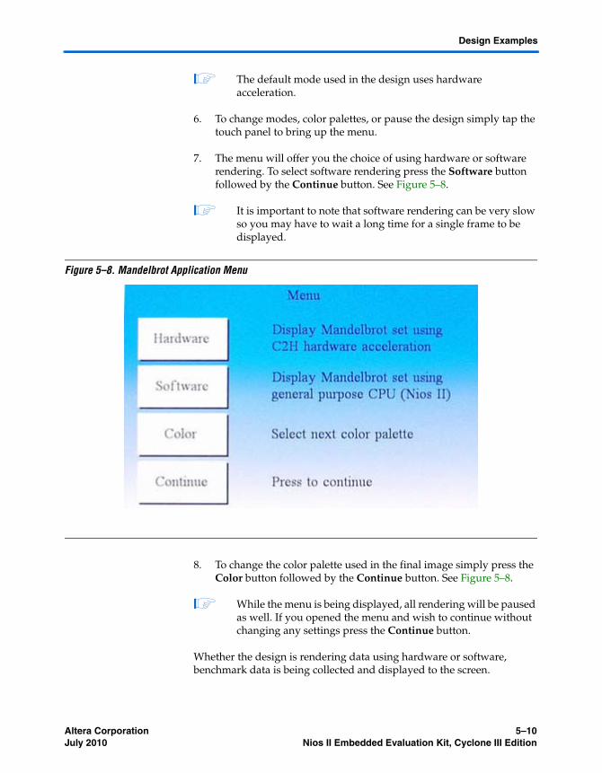
7. The menu will offer you the choice of using hardware or software rendering. To select software rendering press the Software button followed by the Continue button. See Figure 5–8.
1 It is important to note that software rendering can be very slow so you may have to wait a long time for a single frame to be displayed.
Figure 5–8. Mandelbrot Application Menu
8. To change the color palette used in the final image simply press the Color button followed by the Continue button. See Figure 5–8.
1 While the menu is being displayed, all rendering will be paused as well. If you opened the menu and wish to continue without changing any settings press the Continue button.
Whether the design is rendering data using hardware or software, benchmark data is being collected and displayed to the screen.
Altera Corporation 5–10July 2010 Nios II Embedded Evaluation Kit, Cyclone III Edition

Mandelbrot Application
● When hardware rendering is selected the benchmark data is updated every 5 frames.
● When software rendering is selected the benchmark data is updated every frame.
The benchmark data is displayed in the bottom right of the screen and it represents the instantaneous frames per second being rendered and displayed.
Consider the implications of what you have observed: What one would traditionally do with an expensive, power hungry GHz processor was just accomplished using an inexpensive Cyclone III FPGA, running at 100 MHz. Such is the power of hardware acceleration using FPGAs.
Operation
The design performs panning and zooming on the complex plane which gives a video like effect. Every time a new frame is rendered, a new set of coordinates must be calculated. These coordinates contain a center point, zoom factor, and maximum number of iterations. Knowing the center point and zoom factor the top left point of the screen is then determine and passed to the Mandelbrot algorithm. The maximum number of iterations is used to determine how much effort is spent per pixel before it is determined that the point is included in the Mandelbrot set (these points appear as black pixels). The pixel calculation is based on the following software segment:
inline int int_mandelbrot(long long cr, long long ci, int max_iter){ long long xsqr=0, ysqr=0, x=0, y=0; int iter=0; // go ahead and shift these up to the new decimal offset ci = ci<<28; cr = cr<<28; while( ((xsqr + ysqr) < 0x0400000000000000LL) && (iter < max_iter) ) { xsqr = x * x; ysqr = y * y; y = ((2 * x * y) + ci) >> 28; x = (xsqr - ysqr + cr) >> 28; iter++;return(iter);}
5–11 Development Board Version 1.0. Altera CorporationNios II Embedded Evaluation Kit, Cyclone III Edition July 2010
Design Examples
The implementation is fixed point with all values pre-scaled by 0x10000000. The loop will continue until the number of iterations reaches ‘max_iter’ or x2 + y2 converges to the value of 4. This function is called for each pixel so for this design that would be 384000 times since the screen resolution is 800x480. The value of ‘iter’ is used as the index into the color palette which picks the color of the pixel displayed on the screen. Even though the main processor supports dynamic branch prediction and contains cache memory, this operation of filling the screen can be very time consuming.
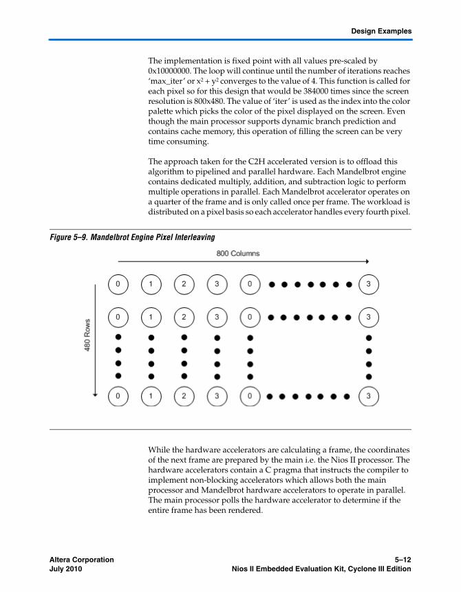
The approach taken for the C2H accelerated version is to offload this algorithm to pipelined and parallel hardware. Each Mandelbrot engine contains dedicated multiply, addition, and subtraction logic to perform multiple operations in parallel. Each Mandelbrot accelerator operates on a quarter of the frame and is only called once per frame. The workload is distributed on a pixel basis so each accelerator handles every fourth pixel.
Figure 5–9. Mandelbrot Engine Pixel Interleaving
While the hardware accelerators are calculating a frame, the coordinates of the next frame are prepared by the main i.e. the Nios II processor. The hardware accelerators contain a C pragma that instructs the compiler to implement non-blocking accelerators which allows both the main processor and Mandelbrot hardware accelerators to operate in parallel. The main processor polls the hardware accelerator to determine if the entire frame has been rendered.
Altera Corporation 5–12July 2010 Nios II Embedded Evaluation Kit, Cyclone III Edition
Application Selector
Application Selector
This application is based on the Application Selector processor system.
You can locate this application in the <install dir>/examples/application_selector folder.
Description: Video, Ethernet and SD Card controller based processor system for LCD Color touch panel control, in-system update using SD Card, remote system update using Ethernet
IP licenses required to ship design:
■ SD/MMC SPI Core IP (with FAT file system) from El Camino■ Triple Speed Ethernet-MAC Core license from Altera (Ordering code
IP-TRIETHERNET)■ Nios II IP evaluation license with Nios II EDS, shipping license from
Altera (Ordering Code IP-NIOS)■ DDR SDRAM memory controller core shipping license from Altera
(comes free with Quartus II Subscription edition as part of Altera IP Base Suite)
Software and middleware licenses required to ship design:
■ NicheStack TCP/IP Network Stack, Nios II Edition free evaluation license available with Nios II EDS, shipping license from Altera (Ordering Code IPSW-TCP/IP-NIOS)
■ MicroC/OS-II real time operating system free evaluation license available with Nios II EDS, shipping license to be purchased from Micrium
1 For more information on how to obtain evaluation or shipping licenses for the above refer to “Licensing the IP” on page 1–11.
The full design example for the application selector utility is available in your Nios II Embedded Evaluation kit installed under the examples directory.
The application selector design examples illustrates several aspects of developing designs and using software device drivers for the Nios II Embedded Evaluation Kit.
■ Interfacing to the LCD touch panel■ Interfacing to the SD Card using the FAT file system■ Implementing a HTTP web server application using the sockets
interface of NicheStack TCP/IP Network Stack, Nios II Edition ■ Implementing remote system update over Ethernet■ Managing multiple FPGA configurations from Flash■ Using the MicroC/OS-II real time operating system
5–13 Development Board Version 1.0. Altera CorporationNios II Embedded Evaluation Kit, Cyclone III Edition July 2010

Design Examples
About the Embedded Web Server
The application selector also features an embedded web server which serves up web pages to enable the remote system update capability. The way this works is as follows:
■ When your kit is connected to a network, the application will serve up a web page
1 The HTTP server looks for content contained in the webserver_html directory at the top level of the SD card. Though default content is provided, the server will read any valid files that are placed into this directory.
■ If DHCP is available, the application will attempt to obtain an IP address from a DHCP server. Otherwise, a static IP address (defined in web_server.h) will be assigned after a time-out.
■ The server can process basic requests to serve HTML, JPEG, and GIF files from the Altera FAT file system on an SD card.
The embedded web server is in no way a complete implementation of a full-featured HTTP server. This example uses the sockets interface.
To learn more about the application selector with embedded web server refer to the source code and design example in the <install_dir>/ examples/application_selector folder.
A good introduction to sockets programming is the book Unix Network Programming by Richard Stevens. Additionally, the text Sockets in C, by Donahoo & Calvert, is a concise and inexpensive text for getting started with sockets programming.
Altera Corporation 5–14July 2010 Nios II Embedded Evaluation Kit, Cyclone III Edition

Altera Corporation DeveloJuly 2010
Appendix A. Video PipelineData Flow
Introduction The video display subsystem embodied in the Nios II Embedded Evaluation Kit designs was intentionally-designed to be modular & flexible to make customizing a snap. The design style used for the video pipeline highlights the use of several simple microcores which can be configured or customized for other video applications.
The video subsystem consists of these operational components, in roughly-logical order:
■ A frame-buffer (which happens to reside in DDR SDRAM memory) ■ A memory-to-stream DMA controller, which reads memory 64 bits
at a time and produces a stream of 64-bit data values. ■ A width (data format adapter) to break the 64-bit stream into
sequential 32-bit (pixel) values. ■ A FIFO ■ A Pixel Format Converter■ Another Data Format Adapter, to produce a stream of 8-bit values. ■ A sync-generator (which you could think of as an LCD-display PHY)
1 If you actually look at the design, there are several other Avalon Streaming components in this flow. These have been omitted from this discussion for clarity because they are not operational. They are just timing-adapters which allow the operational pieces to fit together properly.
Starting from the end of the chain: The sync-generator just takes a stream of 8-bit-wide data values on its streaming input. Three consecutive 8-bit values make a single color pixel (R, G, B, R, G, B…) An start of packet (SOP)-pulse marks the start of each frame. The sync-generator drives external pins so that the pixel-stream appears on the display.
The DMA controller fetches pixel-data from the in-memory frame-buffer and drives it in row-major (raster) order on its streaming output-port and, through the video-subsystem pipeline, to the sync-generator termination.
The system has a FIFO because all systems like this always have FIFOs. It’s there to “take up the slack” and keep the display fed even when the DDR SDRAM memory is unavailable (due to contention, refresh, etc.).
pment Board Version 1.0. A–1Preliminary

The Pixel Format Converter subsystem assumes that the frame-buffer is storing 32-bit pixel values in (0:R:G:B) (8:8:8:8) format. The sync-generator, however, accepts 24-bit values. So the Pixel Format Converter takes-in a stream of 32-bit (0:R:G:B) pixels and produces a stream of 24-bit (R:G:B) values. This is done by throwing-away the unused 8 bits.
Once the Pixel Format Converter has produced a stream of 24-bit (8:8:8) (R:G:B) values, the data format adapter serializes the data into a stream of 8-bit (R, then G, then B) values. This is the input to the sync generator block which produces the horizontal and vertical timing signals.
1 The video pipeline used in the Nios II Standard System is just one implementation for video systems. FPGAs give you the power of flexibility to change this with just a few lines of code. For example, the next section describes what is necessary to support a 5:6:5 pixel format.
Get the full LCD controller Application Note
For more information about the video pipeline and LCD controller, refer to AN527: Implementing an LCD Controller.
Creating a new 5:6:5 Pixel-Format component
The Nios II Standard System is designed to use a 32-bit 0:R:G:B data format. Suppose you wanted to change the entire display subsystem to work with 16-bit 5:6:5 pixels instead of 32-bit 0:R:G:B pixels. This can be accomplished with a few simple steps:
1. Copy the Nios II Standard System into your own project directory.
2. Create a new Verilog module called pixel_converter_565 starting from the Verilog in altera_avalon_pixel_converter.v, modify this Verilog so it has a 16-bit data_in port and a 24-bit data_out port. All the other ports remain the same. You create the data_out value by inserting 8 new bits (3xR, 2xG, and 3xB) at the right points in the 16-bit word to “pad” it to a 24-bit word. You can use either zero- or LSB-padding.
3. Import your Verilog module into SOPC Builder using the Component Editor.
4. From an Nios II Standard System, replace the existing Pixel Format Converter with your new pixel_converter_565 component.
Altera Corporation A–2July 2010 Nios II Embedded Evaluation Kit, Cyclone III Edition

Creating a new 5:6:5 Pixel-Format component
5. Edit the data-format-adapter named lcd_64_to_32_bits_dfa. Change its (Output Interface Parameters)/(Data Symbols Per Beat) from 4 to 2.
● This changes its width-adaptation from 64.32 to 64.16.● Rename it to lcd_64_to_16_bits_dfa.
6. Regenerate your system.
Your software application is now responsible for filling the frame-buffer with aligned 16-bit 5:6:5 pixel data; and the firmware which controls the DMA must be modified to understand the different memory-buffer size implications of 16-bit (instead of 32-bit) pixels.
A–3 Development Board Version 1.0. Altera CorporationNios II Embedded Evaluation Kit, Cyclone III Edition July 2010

Altera Corporation A–4July 2010 Nios II Embedded Evaluation Kit, Cyclone III Edition

Altera Corporation DeveloJuly 2010
Appendix B. ApplicationSelector Details
This section describes some details about the operation of the Application Selector.
SD Card The Application Selector uses the SD Card for storing applications and data used by these applications (such as the pictures used by the picture viewer or the HTML pages used by the Web Server application). The SD Card must be formatted with the FAT 16 file system, and can be any capacity up to 2GB. Long file names are supported.
Application Files Each loadable application consists of two flash files, and an optional text file, all stored on an SD Card.
The first flash file represents the software portion of the example and must be derived from an .ELF file as described in the section of this document titled “Creating Your Own Loadable Applications”. This flash file can be named anything supported by the FAT16 file system, the only restriction being that the name must end with _sw.flash.
The second flash file represents the hardware portion of the example and must be derived from a .SOF file as described in the section of this document titled “Creating Your Own Loadable Applications”. This file can be named anything supported by the FAT 16 file system, the only restriction being that the name must end with _hw.flash
The optional info.txt file contains additional information about the application. In the application selector utility, touching the “Show Info” button while your application is highlighted, brings up a window showing the text contained in this file. The name of this text file must be info.txt, or the application selector will not recognize it.
SD Card Directory Structure
All loadable applications on the SD Card must be located in a top-level directory named Altera_EEK_Applications. Under the Altera_EEK_Applications directory, each application is located in its own subdirectory. The name of that subdirectory is important because the application selector utility uses that name as the title of the application when displaying it in the main menu. The name of the subdirectory is the title that will be displayed for your application in the menu. The subdirectory names can be anything so long as they adhere to the FAT file system long file name rules. Spaces are permitted.
pment Board Version 1.0. B–1
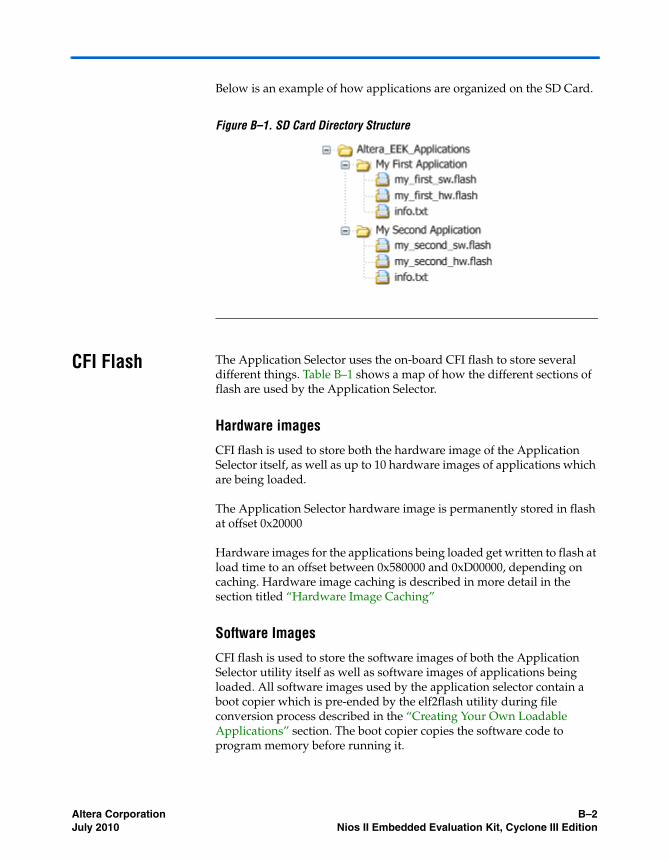
Below is an example of how applications are organized on the SD Card.
Figure B–1. SD Card Directory Structure
CFI Flash The Application Selector uses the on-board CFI flash to store several different things. Table B–1 shows a map of how the different sections of flash are used by the Application Selector.
Hardware images
CFI flash is used to store both the hardware image of the Application Selector itself, as well as up to 10 hardware images of applications which are being loaded.
The Application Selector hardware image is permanently stored in flash at offset 0x20000
Hardware images for the applications being loaded get written to flash at load time to an offset between 0x580000 and 0xD00000, depending on caching. Hardware image caching is described in more detail in the section titled “Hardware Image Caching”
Software Images
CFI flash is used to store the software images of both the Application Selector utility itself as well as software images of applications being loaded. All software images used by the application selector contain a boot copier which is pre-ended by the elf2flash utility during file conversion process described in the “Creating Your Own Loadable Applications” section. The boot copier copies the software code to program memory before running it.
Altera Corporation B–2July 2010 Nios II Embedded Evaluation Kit, Cyclone III Edition

CFI Flash
The Application Selector software image is permanently stored in flash at offset 0x100000
Software images for the applications being loaded get written to flash at load time to offset 0x180000. Software images must be smaller than 4MB, or they will overwrite the application HW images located at offset 0x580000.
Application Boot Code
All applications which are loaded by the application selector must contain a Nios II CPU whose reset address is set to CFI flash at offset 0x0. For this reason, a generic bit of boot code is permanently programmed at offset 0x0 in the CFI Flash as part of the factory recovery image. This boot code is very small and only performs the following functions
■ Flushes the Nios II instruction cache■ Flushes the Nios II instruction pipeline■ Branches to offset 0x180000
Offset 0x180000 is where the application software image is located after being loaded by the Application Selector, so when the FPGA is reconfigured, the Nios II CPU executes this boot code, which branches to the boot copier of the actual application software image, which then copies the application to program memory, then runs the application.
1 The Application Selector relies on a feature of the Cyclone III family of FPGAs called remote update. The remote update feature allows the Nios II CPU, to force the FPGA to reconfigure from a specific location in a parallel flash memory, such as the on-board CFI flash. The way the Application Selector is able to reconfigure itself with a new hardware image is by using Nios II to read the hardware image from the SD Card, program it to some location in CFI flash, then force the FPGA to reconfigure from that location using the remote update feature.
Flash Hardware Image Catalog
The CFI flash holds up to 10 of the most recently loaded application hardware images to speed the load times of applications which are loaded often. To keep track of which hardware images are currently
B–3 Development Board Version 1.0. Altera CorporationNios II Embedded Evaluation Kit, Cyclone III Edition July 2010

stored in flash, a flash image catalog is kept in CFI flash at offset 0x8000. The implementation details of this catalog are described in the Hardware Image Caching section below.
Hardware Image Caching
Copying data from the SD Card to flash is slow due to both the read speed from the SD Card in SPI mode and the write speed of the CFI flash. However the remote update feature allows us to reconfigure the FPGA from anywhere in flash, so we can benefit by persistently holding (caching) a certain number of frequently used application hardware images in flash to avoid having to copy them from the SD Card every time the application is loaded.
The Application Selector utility can cache up to 10 application hardware images in CFI flash. When the user chooses an application to load from the SD Card using the Application Selector, the Application Selector first scans through its catalog of hardware images currently stored in CFI flash to see if any of them match the hardware image being requested. If one of the images cached in CFI flash does match, the Application Selector reconfigures from the offset of that cached hardware image instead of copying the image from SD Card to flash. This significantly reduces the load time.
Caching the hardware images requires the application selector to be able to quickly tell if an image in CFI flash is the same as one on the SD Card. To determine whether a hardware image in flash matches a hardware image on the SD Card, a 32-bit timestamp value is used as a tag. During the file conversion process, the sof2flash utility inserts a 32-bit timestamp in the hardware image .flash file as an S0-type record on the first line of the file. When the Application Selector is about to load a hardware image,
Table B–1. Memory Map of CFI Flash
Flash Size Flash Contents
0x000000 - 0x007FFF 32K Application Boot Code
0x008000 - 0x00FFFF 32K HW Image Catalog
0x010000 - 0x01FFFF 64K Unused
0x020000 - 0x0FFFFF 896K Selector HW Image
0x100000 - 0x17FFFF 512K Selector SW Image
0x240000-0x63FFFF 4M Application SW
0x640000-0xDBFFFF 7.5M Application HW Images
0xD00000 - 0xFFFFFF 3M Unused
Altera Corporation B–4July 2010 Nios II Embedded Evaluation Kit, Cyclone III Edition

Flash Hardware Image Catalog
it inspects the .flash file on the SD Card. If the .flash file contains an S0 record on its first line which contains a 32-bit ASCII-encoded number, it is considered to be a valid timestamp tag.
The Application Selector then scans the flash catalog for entries which contain a matching timestamp. If a matching timestamp value is found, then it means the desired hardware image is already stored in flash, and can be used to directly reconfigure the FPGA without first copying it from the SD-Card into the flash. For details on the flash catalog, refer to the section below titled “Flash Hardware Image Catalog”.
Flash Hardware Image Catalog
The flash hardware image catalog is a simple database which keeps track of what application hardware images are currently stored (cached) in flash. The flash catalog is located in sector 1 of the flash at offset 0x8000, and is 0x8000 (32K) bytes long.
The catalog mechanism uses a scheme referred to as "Zero = Spent, 'F' = Available", or ZSFA. This scheme avoids erasing entire flash sectors when only a few words need to be written to the flash. Using ZSFA, a word in the flash which is 0x0 is considered "spent" and cannot be used to store data. A word which is 0xFFFFFFFF is "available" since it is in its erased state. Every other value is considered a valid entry in the catalog.
The way ZSFA works is that whenever a catalog entry needs to be read, the sector is scanned from its lowest address until the first 0xFFFFFFFF value is encountered. Every non-zero value encountered along the way is a valid catalog entry. When a catalog entry needs to be written, the sector is scanned until the first 0xFFFFFFFF value is found, and the new catalog entry is written to that offset. To erase a catalog entry, you scan for it in the sector, then write 0x0 to it to mark it as "spent". The sector(s) containing the ZSFA catalog only need to be erased once enough data has been stored there that there are no more “available” entry spots available.
Each flash catalog entry consists of two sequential 32-bit words. The first word is the 32-bit timestamp value of a hardware image which is currently in flash. The second word is the 32-bit flash offset of the image itself. Entries are always created and erased as whole units, two 32-bit words at a time.
B–5 Development Board Version 1.0. Altera CorporationNios II Embedded Evaluation Kit, Cyclone III Edition July 2010

Creating Your Own Loadable Applications
It is easy to convert your own Nios II design into an application which is loadable by the Application Selector utility. All you need is a hardware image (a Cyclone III 3C25 .SOF file) and a software image which runs on that hardware (a Nios II .ELF file).
The only restrictions are:
1. The .SOF file must contain a CFI flash component.
2. The .SOF file must contain a Nios II CPU whose reset address is set to CFI Flash at offset 0x00000000.
3. The size of the software image must be no larger than 4MB.
1 If you require a software image larger than 4MB, refer to the section of this document titled “Modifying the Application Selector”
Once you have your working .SOF and .ELF file pair, perform the following steps to convert them to a loadable application selector-compatible application.
1. Copy both the .SOF and .ELF files into a common directory of your choosing. This directory is where you will convert the files.
2. Copy the script:
examples/application_selector/application_utilities/flash_file_conversion_script
to the directory where you copied your .SOF and .ELF files. Optionally, copy it to a directory in the Nios II Command Shell search path i.e. <nios2 install>/bin
3. Open a Nios II Command Shell and change to the directory where you copied the .SOF and .ELF files.
4. Convert the .ELF and .SOF files by running the script:
./eek.sh <elf file>.elf <sof file>.sof
The eek.sh script runs the Nios II Command Line utilities sof2flash and elf2flash to convert the .SOF and .ELF files to application selector-compatible .FLASH files.
1 Feel free to open eek.sh in a text editor to see the exact commands which are run.
Altera Corporation B–6July 2010 Nios II Embedded Evaluation Kit, Cyclone III Edition

Rebuilding the Application Selector
5. You will now see two new files in the directory, <elf file>_sw.flash, and <sof file>_hw.flash. These are the application files you will put on the SD Card
6. Now create a file named info.txt in the same directory.
1 This is the file which will be displayed in the Application Selector when the Show Info button is pressed for your application.
Fill info.txt with some descriptive text about your application’s operation.
7. Create a new subdirectory and name it what you would like the title of your application to be shown as in the application selector.
8. Copy both .flash files and info.txt into the new directory.
9. Using an SD Card reader, copy the directory onto an SD Card into a directory named “Altera_EEK_Applications”. The directory structure on the SD Card should look like this:
Altera_EEK_Applications<Name of Application>
<elf name>_sw.flash<sof_name>_hw.flashinfo.txt
10. Place the SD Card in the Nios II Embedded Evaluation Kit, Cyclone III Edition board, and switch on the power. The Application Selector will start up, and you will now see your application appear as one of the selections
Rebuilding the Application Selector
This section describes how to rebuild the Application Selector utility from source code using the Nios II Software Build Tools. If you are new to developing software on the Nios II processor it is recommended that you first go through the tutorial My First Nios II Software Tutorial. This will walk you through compiling a simple project that runs on the Nios.
1 Throughout this document we will refer to the <Install Directory> which is altera/<version #> /kits/ cycloneIII_3c25_niosII."
B–7 Development Board Version 1.0. Altera CorporationNios II Embedded Evaluation Kit, Cyclone III Edition July 2010
Create a BSP
The first thing that’s needed to build the software project is a board support package (BSP). To create a BSP perform these steps:
1. Open a Nios II Command Shell.
2. Change to the directory:
<Install Directory> examples/ application_selector/ software_examples/ bsp/ hal_application_selector
3. Run the command ./create_this_bsp.
Build the project
The next step is to build the Application Selector project. To build the project, perform these steps:
1. In the Nios II Command Shell, change to the directory:
<Install Directory>examples/
application_selector/software_examples/app/
application_selector
2. Run the command make all.
1 For more information about BSPs and the Nios II Software Build Tools, refer to the Getting Started from the Command Line chapter in volume 2 of the Nios II Software Developer’s Handbook.
Altera Corporation B–8July 2010 Nios II Embedded Evaluation Kit, Cyclone III Edition

Modifying the Application Selector
Build the boot code
To rebuild the boot code which runs when an application is loaded and run from the Application Selector, perform these steps:
1. Open a Nios II Command Shell.
2. Change to the directory:
<Install Directory>examples/
application_selector/application_utilities/
app_selector_boot_code
3. Run the command make.
Modifying the Application Selector
This section discusses the parts of the Application Selector you can modify in order to tailor the utility to your needs
Changing the CFI flash map
If your application needs to use the CFI flash in a particular manner which is not compatible with the Application Selector’s default flash layout, you can modify the way some things are mapped in flash fairly easily.
General Guidelines
If you choose to modify the flash map, take great care in ensuring that you leave enough space in each block for the data you intend to store there. Otherwise, you may overlap sections and the Application Selector utility may overwrite important data and cause a failure.
Also, it is a good idea to completely erase the flash before altering the flash map. This will prevent stale, unused data from accidentally causing errors in the Application Selector Utility.
Application Selector Hardware Image
One of the flash layout restrictions with the Application Selector is that the Application Selector hardware image itself must reside at byte offset 0x20000 in flash. It cannot be changed. This is because the Cyclone III FPGA always performs its first configuration after reset from offset 0x20000.
B–9 Development Board Version 1.0. Altera CorporationNios II Embedded Evaluation Kit, Cyclone III Edition July 2010

Application Hardware Images
The section of flash which is used to hold and cache loadable application hardware images can be adjusted. The adjustments can be made by editing the file:
<Install Directory>examples/
application_selector/software_examples/
app/application_selector/
src/app_selector.h
Edit the lines:
#define AS_HW_IMAGE_OFFSET_START 0X640000
#define AS_HW_IMAGE_OFFSET_END 0xDC0000
to reflect what section of flash you would like to use to hold and cache application hardware images. Note that one hardware image consumes 0xC0000 bytes (6 flash sectors), so ensure that AS_HW_IMAGE_OFFSET_END - AS_HW_IMAGE_OFFSET_START is always greater than or equal to 0xC0000. The Application Selector will cache as many images in this section as it is able to fit. For instance, the default section is 0x780000 bytes in size (60 flash sectors), so it is able to cache up to 10 loadable application hardware images.
Application Selector Software Image
The default location of the Application Selector software image is flash offset 0x100000. This is necessary because flash offset 0x100000 is the reset address of the Nios II CPU in the Application Selector hardware image. It’s recommended that you do not change the location of the Application Selector software image because it also requires changing the reset vector of the Nios II CPU in the Application Selector hardware image, and recompiling that design in Quartus II.
Application Software Image
The application software image can be relocated in flash by performing the following steps:
1. In a text editor, open the file:
Altera Corporation B–10July 2010 Nios II Embedded Evaluation Kit, Cyclone III Edition

Modifying the Application Selector
<install Directory>examples/
application_selector/application_utilities/
app_selector_boot_code/app_selector_boot_code.s
2. Edit the line
#define SW_APP_CODE 0x240000
to reflect the flash offset where you would like to put the loadable application software images. Ensure that there is enough space allocated at that offset to hold your application software images.
3. In a text editor, open the file:
<install Directory>examples/
application_selector/software_examples/
app/application_selector/
src/app_selector.h
4. Edit the line
#define AS_SW_IMAGE_OFFSET 0x240000
to reflect the flash offset where you would like to put the loadable application software images. Ensure that there is enough space allocated at that offset to hold your application software images.
1 You will need to rebuild both the boot code and the application selector utility for these changes to take effect.
Flash Catalog
The flash catalog can be relocated in flash and size-adjusted by performing the following steps.
1. In a text editor, open the file:
B–11 Development Board Version 1.0. Altera CorporationNios II Embedded Evaluation Kit, Cyclone III Edition July 2010

<Installed Directory>examples/
application_selector/software_examples/
app/application_selector/
src/app_selector.h
2. Edit the lines
#define AS_FLASH_IMAGE_CATALOG_OFFSET 0x8000#define AS_FLASH_IMAGE_CATALOG_SIZE 0x8000
to reflect the flash offset where you would like to put flash catalog.
1 You will need to rebuild the boot code for these changes to take effect.
Altera Corporation B–12July 2010 Nios II Embedded Evaluation Kit, Cyclone III Edition

Altera Corporation DeveloJuly 2010
Appendix C. Restoring theFactory Image
Restoring the Original Flash Image (Application Selector)
The Nios II Embedded Evaluation kit is programmed from the factory to configure the FPGA from flash to the application selector. In the course of your development you may need to replace the factory image with your own flash image. To restore the original Flash contents of the Factory Image (i.e. the application selector) perform the following steps:
1. Make sure you have:
a. A PC with Nios II Embedded Evaluation Kit, Quartus II <version 7.2 or later> FPGA design software and Nios II EDS <version 7.2 or later>
b. A USB cable (One should be provided with your kit.)
2. Connect your board to the PC by connecting a USB cable from USB connector (J3) on your board to a USB port on your PC.
3. Tools menu in Quartus II software, launch the Quartus II Programmer and click Auto Detect. The EP3C25F324 device should be detected.
1 If the device is not detected, make sure your hardware is setup for USB-Blaster using the Hardware Setup.. button.
4. Double click on the File field and browse to
Altera/<version #>/kits/cycloneIII_3c25_niosII/factory_recovery/flash_contents/cycloneIII_embedded_evaluation_kit_application_selector.sof
1 The SRAM Object File (SOF) contains a Nios II CPU which can access and program the on-board flash.
5. Click on the Program/Configure checkbox and press Start.
1 You will see a Successfully performed operation info message when the configuration is complete.
6. Launch a Nios II Command Shell from Start>All Programs>Altera> Nios II EDS<version #>Nios II <version #> Command Shell
pment Board Version 1.0. C–1

7. From the Nios II Command Shell change directory to altera/<version #>/kits/cycloneIII_3c25_niosII/factory_recovery/flash_contents
8. From the Nios II Command Shell, program the factory image into flash by typing the command:
Nios2-flash-programmer --base=0x04000000 restore_cycloneIII_3c25.flash
1 If you get the error message: No CFI table found at address <address> Leaving target processor paused then check that either the address is correct (i.e. hex four million, six zeros after the 4) or that you have tow “-“ characters before the “base”
9. You should now be able to reset the board to start the application selector.
Rebuilding the Application Selector from Source Files
This section describes the process of rebuilding the factory recovery image from source files. You may wish to modify and rebuild the factory recovery image you’ve modified the application selector or boot code and would like a single recovery file which includes your modifications. Keep in mind that any modifications you make to the application selector or boot code, may make them incompatible with existing applications.
Each portion of the factory recovery image is described below, with instructions on how to create it and program it to flash. The last section here, titled “Combining factory recovery image files”, includes instructions for creating a single factory recovery image that you can program into flash at any time to restore the factory configuration of the Embedded Evaluation Kit board.
To perform the tasks illustrated in this section, you must first open aNios II command shell.
Boot Code The first portion of the factory recovery image is the application boot code, located at flash offset 0x0. Appendix B describes the functionality of the boot code and how to rebuild it from the source files.
Building the boot code produces a file named app_selector_boot_code.srec. This file can be directly programmed to flash using nios2-flash-programmer in the Nios II command shell.
1. From the Nios II Command Shell navigate to altera/<version # >/ cycloneIII_3c25_niosII/examples/application_selector/application_utilities/application_selector_boot_code
Altera Corporation C–2July 2010 Nios II Embedded Evaluation Kit, Cyclone III Edition

Hardware Image Catalog
2. From the Nios II Command Shell type:
nios2-flash-programmer -–base=0x4000000
Hardware Image Catalog
The hardware image catalog section of flash is located at offset 0x8000. This section holds the locations of the currently cached hardware images in flash. Any time a factory recovery is performed, this section of flash should be erased to ensure no stale catalog entries exist. To erase this section of flash, enter the command:
nios2-flash-programmer --base=0x4000000 –-erase 0x8000+0x8000
After erasing this section, you may wish to read back the erased contents into a file, so that you can combine this file into the final factory recover image. The command to read back this section into a file named catalog.srec is:
nios2-flash-programmer --base=0x4000000 --read catalog.flash --read-bytes 0x8000+0x8000
Application Selector Hardware Image
The application selector hardware image section contains the FPGA hardware image for the application selector utility. This section is located at flash offset 0x20000. The FPGA gets configured with this image upon power-up and after a board reset. The file you will need to create this portion of the factory recovery image is named cycloneIII_embedded_evaluation_kit_application_selector.sof, and is located in the application selector’s Quartus II project directory. The command needed to create the application selector hardware portion of the factory recovery image is:
From the Nios II Command Shell navigate to altera\<version #> \kits\cycloneIII_3c120_niosII_dev\examples\application_selector.
From the Nios II Command Shell type:
sof2flash --activeparallel --offset=0x20000 --input= cycloneIII_ embedded_ evaluation_kit _application_selector.sof --output= appsel_hw.flash
1 The command above converts the application selector SOF file to hardware flash image.
To program this .flash file to flash, run the command:
nios2-flash-programmer --base=0x4000000 appsel_hw.flash
C–3 Development Board Version 1.0. Altera CorporationNios II Embedded Evaluation Kit, Cyclone III Edition July 2010

Application Selector Software Image
The final portion of the factory recovery image is the application selector software image. This section is located at flash offset 0x100000. The Nios II processor resets to this address and runs this code every time the FPGA gets configured with the application selector hardware image. The file you will need to create this portion of the factory recovery image is named ext_flash.flash, and is located in the application selector software project directory. You need to run the following command from the application selector software project directory to create ext_flash.flash if it does not already exist:
make flash
Once “ext_flash.flash” is created, you can program it into flash with the following command:
nios2-flash-programmer --base=0x4000000 ext_flash.flash
Combining factory recovery image files
Once you’ve created flash (or srec) files for all the sections of the factory recovery image, you can combine them all into one file using the cat command:
cat app_selector_boot_code.srec catalog.flash appsel_hw.flash ext_flash.flash > temp_restore.flash
However, you are still not done. Some of the individual files we combined contained non-data records in them. Some non-data records, such as “S0” records cannot appear anywhere in an SREC file except for the beginning, so you want to remove all the non-data records from the final factory recovery image. Data record types, are S1, S2, and S3, so you want to remove all the other types of records (S0, S5, S7, S8, and S9).You can use the command “sed” to perform this task. Use the following command to remove all non-data records from the new factory recovery image file:
sed '/^S[05789]/ d' temp_restore.flash >restore_cycloneIII _3c25.flash
You can now restore the Embedded Evaluation Kit board to its factory state by running the command
nios2-flash-programmer --base=0x4000000 restore_cycloneIII _3c25.flash
Altera Corporation C–4July 2010 Nios II Embedded Evaluation Kit, Cyclone III Edition

Altera Corporation DeveloJuly 2010
Appendix D. FrequentlyAsked Questions
This section below explains the frequently asked questions of Nios II Embedded Evaluation Kit.
Why is my SOF time-limited?
Several IP cores in the example designs (Nios II processor core, DDR SDRAM memory core, TSE MAC core) are evaluation versions available as OpenCore Plus IP cores. OpenCore Plus hardware evaluation supports the following two modes of operation:
● Tethered—requires a JTAG connection between your board and the host computer. If tethered mode is supported by all megafunctions in a design, the device can operate for a longer time or indefinitely
● Untethered—the design runs for a limited time
To generate non time limited SOF files you will need to purchase shipping licenses for any OpenCore Plus IP cores in your system. Contact your local sales offices to purchase the license.
http://www.altera.com/corporate/contact/con-index.html
What are Ready-to-Run Demonstrations?
Ready-to-run demonstrations are binary (flash) files of processor systems that can be programmed to flash or selected and loaded from the LCD touch panel. Ready-to-run demonstrations provide a quick and easy way to evaluate Nios II based processor systems built for applications such as automotive graphics, industrial controls, consumer graphic user interfaces and more.
Most ready-to-run demonstrations have been provided by Altera's partners and showcase IP, operating systems and software tools.
Where can I find Ready-to-Run Demonstrations?
For the Nios II Embedded Evaluation Kit (NEEK), there are many ready-to-run demonstrations available on the sd-card. A menu listing all the demonstrations stored on the SD-Card appears when the NEEK is first powered up. The ready-to-run demonstrations that you see on the
pment Board Version 1.0. D–1

display of the Nios II Embedded Evaluation Kit can be found in the kit installation directory at <Install Dir>\factory_recovery\ sdcard_contents\ Altera_EEK_Applications
What is in a ready-to-run demonstration ?
A ready-to-run demonstration consists of the following files:
■ Binary image (.flash format) containing the FPGA hardware image■ Binary image (.flash format) containing the software application■ Optional info.txt file containing a brief description of the
demonstration
How do ready-to-run demonstrations get loaded from the SD card to the FPGA?
When you select one of these demonstrations from main menu on the LCD screen, the default design called application selector copies these images from the SD Card to the Flash memory and reconfigures the FPGA with your chosen demonstration application.
Where can I get more ready-to-run demonstrations?
To get more information about the ready-to-run demonstrations:
1. For usage instructions use the LCD Touch Screen to highlight the demonstration and press the Info button.
2. In addition to the prepackaged ready-to-run SD Card demonstration applications which come with the Nios II Embedded Evaluation Kit, Cyclone III Edition, more are available from Altera or through third party vendors. For more information about ready-to-run SD Card demonstration applications, refer to the Nios II Embedded Evaluation Kit (NEEK), Cyclone III Edition page.
3. For more information, refer to the Nios II Embedded Evaluation Kit (NEEK), Cyclone III Edition User Guide.
Where can I get full Quartus II projects and source code for ready-to-run demonstrations?
Altera's partners can provide full Quartus II projects, source code, development tools and even design services to get you up and running developing products. You will find links to partners from Nios II Embedded Evaluation Kit (NEEK), Cyclone III Edition page.
Altera Corporation D–2July 2010 Nios II Embedded Evaluation Kit, Cyclone III Edition

Why do I get the error “Can't find valid feature line for core SD_MMC_SPI_CORE (EC11_0002) in current license;Error: Error (10003): Can't open encrypted VHDL or Verilog HDL file” when I try to re-generate the Nios II Standard hardware design?
The Nios II Standard hardware design contains the SD MMC SPI CORE which is a component that has been provided by a third party vendor, El Camino. To compile this core in your SOPC Builder system, you will need to get a license from El Camino. However, if your particular application has no need to access the SD Card then you do not need to include the SD Card core in your system. Simply uncheck this core or delete it and re-generate the system. You should now be able to rebuild the hardware system without error.
When your hardware and software image is ready you can add your design to be loadable by the application selector by following the steps listed in the FAQ: “How do I add my own design so the Application Selector can find and run it?”
Where can I get the SD-Card Controller IP License?
If your design requires access to the on-board SD Card then you can request an evaluation license or purchase the SD-Card Controller IP, drivers and FAT File system from El Camino.
El Camino GmbHLandshuter Str. 1D-84048 MainburgGermany
Tel. +49 - 8751 - 8787 - 0Fax +49 - 8751 - 842876Web: www.elcamino.de E-mail: [email protected]
How do I add pictures so the Picture Viewer Application can find them?
1. Connect the SD-Card reader provided in the Nios II Embedded Evaluation Kit to your PC via a USB port.
2. Remove the SD-Card and place in the SD-Card Reader.
3. Add any .JPEG or .BMP file to the “images” folder on the SD Card.
D–3 Development Board Version 1.0. Altera CorporationNios II Embedded Evaluation Kit, Cyclone III Edition July 2010

4. Re-insert the SD-Card in the Nios II Embedded Evaluation Kit board.
The next time you run the Picture Viewer application, these new files will be found.
How do I add my own design so the Application Selector can find and run it?
The Nios II Embedded Evaluation Kit provides an elegant way to add designs such that a user can scroll through and select the design of choice using the application selector. Details of the application selector can be found in the ‘readme.txt’ located in the application_selector folder under examples in the Nios II Embedded Evaluation Kit directory.
To convert your own Nios II design into an application which is loadable by the Application Selector utility you will need the following
1. A hardware image (a Cyclone III 3C25 .SOF file)
2. A software image which runs on that hardware (a Nios II .ELF file).
3. An SD Card reader
f For a step by step instructions refer to section in Appendix B of this document entitled “Creating Your Own Loadable Applications”
Where do I go to get more designs for the Nios II Embedded Evaluation Kit?
For more information about the latest demonstrations available for download to your Nios II Embedded Evaluation kit, refer to the Nios II Embedded Evaluation (NEEK), Cyclone III Edition page.
You will be able to download the designs to your local drive and add them to your SD Card by placing them in the SD Card folder entitled Altera_EEK_Appliations. The application selector should automatically detect these new designs and load them on to your kit.
How do I open a design example in the Nios II IDE?
Several example applications have been provided to you in source code form so that you can use them to learn how to develop your own software applications. The example applications have been provided in the Nios II Software Build flow format, i.e. in the form of application (APP) and board support package (BSP).
Altera Corporation D–4July 2010 Nios II Embedded Evaluation Kit, Cyclone III Edition

If you would like to open these Nios II Software Build flow projects to the Nios II IDE for debugging purposes, then you will import the app and bsp projects into the Nios II IDE.
For step by step instructions on importing a Nios II Software Build flow project in to the Nios II IDE, refer to the software tutorial “My First Nios II Software Application” in the documents/tutorials/software_tutorials folder of the Nios II Embedded Evaluation kit directory.
How do I restore the factory image?
To restore the factory image, perform the following steps:
1. Using the Quartus II Programmer, configure the FPGA with the SOF file:
altera/<version #>/kits/cycloneIII_3c25_niosII/examples/application_selector/cycloneIII_embedded_evaluation_kit_applicatoin_selector.sof
2. Open a Nios II Command Shell and change to the directory:
altera/<version #>/kits/ cycloneIII_3c25_niosII/factory_recovery/flash_contents
3. In the Nios II Command Shell, program the factory image into flash with the command:
nios2-flash-programmer base=0x04000000
restore_cycloneIII_3c25.flash
1 If you get the error message: No CFI table found at address <address> Leaving target processor paused
Check that either the address is correct (hex four million - i.e. 6 zeroes after the 4) or that you have two "-" characters before "base".
4. You should now be able to reset the board to start the Application Selector.
How do I re-build the factory image?
To re-build the factory image refer to Appendix C, Restoring the Factory Image.
D–5 Development Board Version 1.0. Altera CorporationNios II Embedded Evaluation Kit, Cyclone III Edition July 2010

Altera Corporation D–6July 2010 Nios II Embedded Evaluation Kit, Cyclone III Edition
Altera Corporation July 2010
Additional Information
Revision History The table below displays the revision history for the chapters in this user guide.
How to Contact Altera
For the most up-to-date information about Altera products, refer to the following table:
Chapter Date Version Changes Made
All July 2010 1.2 ● Removed “Licensing the Quartus II Software” section.● Updated Figure 1–1 on page 1–8.● Updated “Installing the Nios II Embedded Evaluation Kit, Cyclone III
Edition” on page 1–7.● Updated “Installing the Quartus II Web Edition Software” on
page 1–9.● Updated “Further Information” on page i–ii.● Updated Table B–1 on page B–4.● Updated “Application Hardware Images” on page B–10 and
“Application Software Image” on page B–10.● Updated Copyright information.
All August 2008 1.1 ● Second publication
All November 2007 1.0 ● First publication.
Information Type Contact Note (1)
Technical support www.altera.com/mysupport/
Technical training www.altera.com/training/
Technical training services [email protected]
Product literature www.altera.com/literature
Product literature services [email protected]
FTP site ftp.altera.com
Note to table:(1) You can also contact your local Altera sales office or sales representative.
Info–iPreliminary

Additional Information Further Information
Further Information
For other related information, refer to the following websites:
Typographic Conventions
This document uses the typographic conventions shown below.
For More Information About Refer to
Cyclone III handbook www.altera.com/literature/lit-cyc3.jsp
Cyclone III reference designs www.altera.com/products/devkits/altera/kit-cyc3-embedded.html
eStore if you want to purchase devices
www.altera.com/buy/devices/buy-devices.html
Cyclone III Orcad symbols www.altera.com/support/software/download/pcb/pcbpcb_index.html
Nios® II 32-bit embedded processor solutions
www.altera.com/technology/embedded/emb-index.html
Visual Cue Meaning
Bold Type with Initial Capital Letters
Command names, dialog box titles, checkbox options, and dialog box options are shown in bold, initial capital letters. Example: Save As dialog box.
bold type External timing parameters, directory names, project names, disk drive names, filenames, filename extensions, and software utility names are shown in bold type. Examples: fMAX, \qdesigns directory, d: drive, chiptrip.gdf file.
Italic Type with Initial Capital Letters
Document titles are shown in italic type with initial capital letters. Example: AN 75: High-Speed Board Design.
Italic type Internal timing parameters and variables are shown in italic type. Examples: tPIA, n + 1.
Variable names are enclosed in angle brackets (< >) and shown in italic type. Example: <file name>, <project name>.pof file.
Initial Capital Letters Keyboard keys and menu names are shown with initial capital letters. Examples: Delete key, the Options menu.
“Subheading Title” References to sections within a document and titles of on-line help topics are shown in quotation marks. Example: “Typographic Conventions.”
Courier type Signal and port names are shown in lowercase Courier type. Examples: data1, tdi, input. Active-low signals are denoted by suffix n, e.g., resetn.
Anything that must be typed exactly as it appears is shown in Courier type. For example: c:\qdesigns\tutorial\chiptrip.gdf. Also, sections of an actual file, such as a Report File, references to parts of files (e.g., the AHDL keyword SUBDESIGN), as well as logic function names (e.g., TRI) are shown in Courier.
Altera Corporation Info–ii

Typographic Conventions Nios II Embedded Evaluation Kit, Cyclone III Edition
1., 2., 3., anda., b., c., etc.
Numbered steps are used in a list of items when the sequence of the items is important, such as the steps listed in a procedure.
■ ● • Bullets are used in a list of items when the sequence of the items is not important.
v The checkmark indicates a procedure that consists of one step only.
1 The hand points to information that requires special attention.
c A caution calls attention to a condition or possible situation that can damage or destroy the product or the user’s work.
w A warning calls attention to a condition or possible situation that can cause injury to the user.
r The angled arrow indicates you should press the Enter key.
f The feet direct you to more information on a particular topic.
Visual Cue Meaning
Info–iii Altera CorporationPreliminary July 2010

Additional Information Typographic Conventions
Altera Corporation Info–iv