
Integration of in situ RHEED with magnetron sputter ...
146
Integration of in situ RHEED with magnetron sputter deposition for atomic layer controlled growth By Jacob P. Podkaminer A dissertation submitted in partial fulfillment of the requirements for the degree of Doctor of Philosophy (Materials Science) at the UNIVERSITY OF WISCONSIN‐MADISON 2016 Date of final oral examination: 04/19/2016 The dissertation is approved by the following members of the Final Oral Committee: Chang-Beom Eom, Professor, Materials Science and Engineering Mark S. Rzchowski, Professor, Physics Robert F. McDermott, Professor, Physics Xudong Wang, Professor, Materials Science and Engineering Thomas Tybell, Professor, Electronics and Telecommunications
Transcript of Integration of in situ RHEED with magnetron sputter ...
Integration of in situ RHEED with magnetron sputter deposition for
atomic layer controlled growth
By
Jacob P. Podkaminer
A dissertation submitted in partial fulfillment of
the requirements for the degree of
Doctor of Philosophy
(Materials Science)
at the
UNIVERSITY OF WISCONSIN‐MADISON
2016
Date of final oral examination: 04/19/2016
The dissertation is approved by the following members of the Final Oral Committee:
Chang-Beom Eom, Professor, Materials Science and Engineering
Mark S. Rzchowski, Professor, Physics
Robert F. McDermott, Professor, Physics
Xudong Wang, Professor, Materials Science and Engineering
Thomas Tybell, Professor, Electronics and Telecommunications

i

ii
Abstract
Integration of in situ RHEED with magnetron sputter deposition for
atomic layer controlled growth
Jacob P. Podkaminer
Work completed under the supervision of Professor Chang-Beom Eom
University of Wisconsin – Madison
Epitaxial thin films continue to be one of the most promising topics within electronic
materials research. Sputter deposition is one process by which these films can be formed and is a
widely used growth technique for a large range of technologically important material systems.
Epitaxial films of carbides, nitrides, metals, oxides and more can all be formed during the sputter
process which offers the ability to deposit smooth and uniform films from the research level up
to an industrial scale. This tunable kinematic deposition process excels in easily adapting for a
large range of environments and growth procedures. Despite the vast advantages associated with
sputter deposition, there is a significant lack of in situ analysis options during sputtering. In
particular, the area of real time atomic layer control is severely deficient.
Atomic layer controlled growth of epitaxial thin films and artificially layered
superlattices is critical for both understanding their emergent phenomena and engineering novel
material systems and devices. Reflection high-energy electron diffraction (RHEED) is one of the
most common in situ analysis techniques during thin film deposition that is rarely used during

iii
sputtering due to the strong permanent magnets in magnetron sputter sources and their effect on
the RHEED electron beam. In this work we have solved this problem and designed a novel way
to deter the effect of the magnets for a wide range of growth geometries and demonstrate the
ability for the first time to have layer by layer control during sputter deposition by in situ
RHEED. A novel growth chamber that can seamlessly change between pulsed laser deposition
and sputtering with RHEED for the growth of complex heterostructures has been designed and
implemented. Epitaxial thin films of LaAlO3, La1-xSrxMnO3, and SrRuO3 have all been
deposited by sputtering and shown to exhibit clear and extended RHEED oscillations. To solve
the magnet issue, a finite element model has been constructed to predict and avoid the deflection
of the electron beam in many geometries. Together, this creates the possibility for RHEED to
become a widely used real time analysis tool with sputter deposition with far reaching
applications and potential.

iv
Acknowledgements
I will never forget the day that I was driving through the Rocky Mountains with friends
heading for Vail when, I received a phone call from Professor Chang-Beom Eom. He was
calling to make me an offer for a Research Assistant position in his lab and I had zero bars of
service. I knew this could easily be one of the most important calls of my life and naturally I
was panicking. In the end, I moved to Madison to work for Professor Eom and he has provided
me with continuous and steadfast support since. I cannot thank him enough for the number of
doors he has opened for me and the opportunities he has given me. In many ways he has enabled
the child inside me with the ability to play with all the toys in the lab and gave me the freedom to
get involved in so many projects when my mind wanders. It has been a truly great experience
and built a relationship that will continue for many years.
My fellow co-workers and collaborators, past and present, deserve a standing ovation as
well. Throughout the years they have helped me, pushed me, and put up with me. So many
great friendships and bonds have been built making this experience truly outstanding. In
particular, I would like to thank Chad Folkman for being my mentor early on and still, Camilo
for being a great housemate and research partner, Wittawat and Josh for going through all the
years of PhD work together and supporting each other, and Sangwoo who was my officemate,
mentor, friend, and collaborator. Bruce Davidson with whom I spent many a nights at several
synchrotrons, contributed to much of this work and is now a good friend. The entire Oxide Lab
deserves recognition and I thank you all. Additionally, all my friends and experiences I have had
outside of the lab have made this time balanced and enjoyable. A recognition is due to all those
that have contributed to my “normal person life”.

v
My family has been my rock throughout all of this. The PhD process is full of peaks and
extremely deep valleys at times. My parents, Joel and Tina, my sister Annie, and all my
extended family, they have been there through it all! They seem interested when I describe my
research, and were understanding when I vented my issues. No matter the situation they were
there for me and have given me the tools to succeed in life from day one. So much of my
success I owe to them.
And finally, my soon to be wife, Gina Furlano deserves the biggest thank you of all. You
came into my life when I was at my lowest point and almost immediately carried me to the
highest peak. You have been there for me day in and day out with continuous words of
encouragement. Through the good times and the bad, happiness has always been found in your
company. You never cease to amaze me and inspire me with your strength, independence,
positivity, and balance. I cannot wait for what our future holds. Thank you.
-Dedicated to Jack Stanley Podkaminer & Chis Bond

vi
Table of Contents
Abstract ....................................................................................................................................... ii
Acknowledgements ................................................................................................................. iv
Table of Contents .................................................................................................................... vi
List of Figures .......................................................................................................................... ix
Preface ........................................................................................................................................ xi
1. Introduction ...................................................................................................................... 1
1.1. Motivation ............................................................................................................... 1
1.2. Oxide Thin Films .................................................................................................... 4
1.3. Deposition techniques ............................................................................................. 6
1.3.1. Molecular beam epitaxy (MBE) .............................................................. 8
1.3.2. Pulsed laser deposition (PLD) ............................................................... 10
1.3.3. Sputter deposition .................................................................................. 13
1.4. Reflection high energy electron diffraction (RHEED) ......................................... 16
1.5. Outline of thesis .................................................................................................... 21
1.6. References for chapter 1 ....................................................................................... 24
2. PLD-Sputtering Hybrid with RHEED .................................................................. 31
2.1. Introduction ........................................................................................................... 31

vii
2.2. System design ....................................................................................................... 35
2.2.1. Deposition chamber ............................................................................... 35
2.2.2. LabView Control Program ..................................................................... 42
2.3. Metal – Oxide Heterostructures ............................................................................ 44
2.4. Conclusions ........................................................................................................... 57
2.5. References for chapter 2 ....................................................................................... 58
3. Two-dimensional electron gas (2DEG) at the LaAlO3/SrTiO3 interface by
sputtering........................................................................................................................ 61
3.1. Introduction ........................................................................................................... 61
3.2. Film growth and structural characterization ......................................................... 66
3.3. Electric characterization ........................................................................................ 70
3.4. Conclusions ........................................................................................................... 73
3.5. References ............................................................................................................. 74
4. In situ RHEED during oxide sputtering ............................................................... 78
4.1. Introduction ........................................................................................................... 78
4.2. RHEED with magnetron sputtering ...................................................................... 80
4.2.1. Scattering due to gas .............................................................................. 81
4.2.2. Deflection due to magnetic field ............................................................ 85
4.3. RHEED intensity oscillations ............................................................................... 89
4.3.1. LaAlO3/SrTiO3 ....................................................................................... 91

viii
4.3.2. La0.7Sr0.3MnO3/SrTiO3 ........................................................................... 95
4.3.3. SrRuO3/SrTiO3 ....................................................................................... 99
4.4. Conclusions ......................................................................................................... 104
4.5. Reference for chapter 4 ....................................................................................... 105
5. Finite element modeling ............................................................................................ 110
5.1. Introduction ......................................................................................................... 110
5.2. Modeling parameters .......................................................................................... 112
5.3. Single and two gun 90° off-axis geometries ....................................................... 112
5.4. Two antisymmetric configurations ..................................................................... 120
5.5. Generic solution .................................................................................................. 122
5.6. Antisymmetric SRO growth ............................................................................... 125
5.7. Conclusions ......................................................................................................... 129
5.8. References for chapter 5 ..................................................................................... 130
6. Summary and future thoughts ............................................................................... 131

ix
List of Figures
Figure 1.1. The classic perovskite unit cell..................................................................................... 5
Figure 1.2. Common lattice parameters and strain states.. ............................................................. 7
Figure 1.3. A schematic of an oxide-MBE chamber ...................................................................... 9
Figure 1.4. Example of sputter processes ..................................................................................... 13
Figure 1.5. Schematic representation of RHEED intensity oscillations ....................................... 20
Figure 2.1. MgO surface after exposure to air .............................................................................. 33
Figure 2.2. Schematic layout of the "hybrid" deposition chamber ............................................... 36
Figure 2.3. The mirrored growth geometries ................................................................................ 37
Figure 2.4. Growth sequence static RHEED images .................................................................... 46
Figure 2.5. Structural characterization .......................................................................................... 50
Figure 2.6. Two step Al2O3 RHEED progression ......................................................................... 52
Figure 2.7. Surface images of Al2O3 and Re ................................................................................ 53
Figure 2.8. TEM analysis of the heterostructure ........................................................................... 54
Figure 2.9. XRD of the Al/Al2O3/Re trilayer ................................................................................ 55
Figure 2.10. Quality factor measurements of the trilayer ............................................................. 56
Figure 3.1. Layering structure in the LAO/STO heterointerface .................................................. 63
Figure 3.2. Carrier concentration as a function of number of unit cells ....................................... 64
Figure 3.3. Structural characterization of the LAO/STO heterostructure ..................................... 68
Figure 3.4. Surface topography of the STO substrate and LAO film ........................................... 69
Figure 3.5. Transport properties of the sputtered LAO/STO heterostructure. .............................. 70
Figure 3.6. Room-temperature conductive-AFM (c-AFM) switching ......................................... 72

x
Figure 4.1. The differential scattering cross section for Ar and O atoms ..................................... 83
Figure 4.2. Scattering comparison for Ar and O2 gas ................................................................... 84
Figure 4.3. Schematic of the growth chamber .............................................................................. 88
Figure 4.4. Sputter deposition effects on RHEED. ....................................................................... 89
Figure 4.5. RHEED oscillations during a LaAlO3 growth on a SrTiO3 substrate ........................ 92
Figure 4.6. Ex situ structural and surface analysis of the LAO/STO film .................................... 94
Figure 4.7. La0.7Sr0.3MnO3 growth on a SrTiO3 substrate showing clear RHEED intensity
oscillations ........................................................................................................................ 96
Figure 4.8. X-ray and AFM measurements of the LSMO film .................................................... 98
Figure 4.9. RHEED oscillations from SRO growth .................................................................... 100
Figure 4.10. Topographic and structural characterization of the SRO film ................................ 102
Figure 5.1. 2-dimensional cross-sections showing the magnetic field close to the sample for the
single gun, two gun symmetric and two gun antisymmetric magnet polarities .............. 114
Figure 5.2. Finite element simulations showing electron beam deflection in single gun,
symmetric, and antisymmetric sputter source geometries and their resulting RHEED
pattern ............................................................................................................................. 116
Figure 5.3. Finite element simulations side view ....................................................................... 118
Figure 5.4. Magnetic field simulations for the two possible antisymmetric configurations ....... 121
Figure 5.5. Confocal and high rate off-axis antisymmetric setups ............................................. 123
Figure 5.6. An on-axis sputter arrangement with symmetric sputter sources centered around the
substrate .......................................................................................................................... 124
Figure 5.7. RHEED intensity oscillations during SRO growth .................................................. 127

xi
Preface
The work presented in this thesis has been the culmination of the author’s research over
the last six years. This work is primarily orchestrated and conducted by the author but naturally
done in collaboration with several other groups. The author has performed all of the film
growth, structural and surface characterization, and worked closely with J. Patzner to create the
finite element models. Chapter 2 is both original and work that has been adapted from APL
Mater. 1, 042115 (2013). The TEM in Chapter 2 was performed by Y. Zhang and X.Q. Pan.
The SSQCD devices and microwave characterization in Chapter 2 were performed by U. Patel,
Y. Gao, and R. McDermott. The films for the SSQCD were grown together with K.H. Cho. The
Al/MgO/Re trilayer XRD measurement was done by C.M. Folkman who also helped build the
hybrid chamber. The electrical characterization in Chapter 3 was done in collaboration with T.
Hernandez and M. Rzchowski, and the c-AFM work was done by M. Huang and J. Levy.

1
1. Introduction
1.1. Motivation
The focus of this thesis is on pushing the boundaries of thin film deposition in order to
create new material systems and their potentially novel electronic states. As Richard Feynman
said in 1959:
But it is interesting that it would be, in principle, possible (I think) for a physicist to
synthesize any chemical substance that the chemist writes down. Give the orders and the
physicist synthesizes it. How? Put the atoms down where the chemist says, and so you
make the substance. The problems of chemistry and biology can be greatly helped if our
ability to see what we are doing, and to do things on an atomic level, is ultimately
developed – a development which I think cannot be avoided.1
This prophecy has been a strong motivation for this thesis. While there are many interesting
material systems present in nature, the ability to create “artificial” materials can open the door
for new and exciting phenomenon to be discovered. While Feynman’s prediction has become
reality to a certain degree, there is always further development, which is what we aim to do.
Oxide materials, in particular the perovskite family, are an excellent place to pursue the
enhancement of atomic level control and the creation of new materials due to the nature of the

2
ABO3 crystal structure. While there are some restrictions, in general the A and B constituent
elements are freely interchanged to access new materials properties. This gets even more
exciting when combing two distinct perovskites together, which in general is feasible due to the
same parent crystal structure and oxide nature. The exciting physics and material science that
can be discovered and engineered at the materials interface and the coupling between their
discrete electronic properties is what drives this field in general.
To obtain this type of scientific exploration, perfect intrinsic materials are desirable, free
of defects and extrinsic contaminates. Epitaxial thin films provide the ideal platform for
developing new and exciting electronic materials for several reasons. First, thin film deposition
brings us closer to Feynman’s idea for creating new materials since it is a growth process that is
on the nanometer to sub-nanometer scale already. Second, most epitaxial deposition processes
take place in controlled vacuum environments, which limits the exposure to external
contaminants. In this way, interfaces can be kept as close to pristine as possible. Third, coherent
film growth facilitates the engineering of physical states into the material system which are
otherwise extremely challenging to obtain in bulk materials. An excellent example of this is thin
film epitaxial strain which can reach equivalent pressures in the range of GPa and can
significantly affect the material property such as increasing the superconducting Tc.2,3
And
finally, it is possible to deposit complex heterostructures and superlattices to build material
stacks that otherwise do not exist. This is not an exhaustive list of the advantages to epitaxial
thin film growth and while there are disadvantages and limitations compared to polycrystalline
or bulk materials, single crystalline thin films are a direct route to achieving and probing the
intrinsic properties of a material.

3
While epitaxial thin films are the perfect platform for pushing the bounds of material
properties, a way to “see” what is happening during the deposition is ultimately needed to garner
true atomic level control. For this type of in situ control, reflection high energy electron
diffraction (RHEED) is often utilized. Real time monitoring of the RHEED pattern provides
information regarding the interface state, lattice relaxation, and growth dynamics, and allows for
precise thickness control. In molecular beam epitaxy (MBE), RHEED is also commonly used
for sub unit cell thin film growth which is approaching the level that Feynman discusses.
Despite the popularity of RHEED, there is still room to improve. For instance, only recently has
pulsed laser deposition (PLD) shown that it can approach the type of atomic control that is
observed via RHEED in MBE.4 On the other hand, despite sputter deposition being a prominent
growth technique for scientific research and at an industrial level for a wide range of materials, it
rarely is used in conjunction with in situ RHEED.5 This has severely inhibited sputter
deposition’s ability to excel in the area of precise epitaxial oxide heterostructure growth to the
level that MBE and PLD has.
The lack of in situ analysis during sputter deposition is the primary motivation for this
thesis. The goal has been to determine precisely what limits the integration of RHEED with
sputtering, find ways around the limitations, and ultimately solve the problems to either remove
or mitigate issues to the point that they are not significant factors. Meanwhile, the goal has also
been to use RHEED with sputtering to grow interesting and novel heterostructures, from the
LaAlO3/SrTiO3 two-dimensional electron gas (2DEG) to epitaxial capacitive stacks for solid
state quantum computing devices (SSQCDs). Following the wisdom of Feynman, it is also of
interest for this thesis that this technique be used to further approach the ability to build any
material system desired by placing atoms where we want them. As such, the future of this area

4
of research is geared towards depositing materials that are outside the realm of possibility for
both MBE and PLD and require the precise control provided by in situ RHEED monitoring
during sputtering.
1.2. Oxide Thin Films
Complex oxides have some of the most diverse physical properties known to a single
class of materials. For example, in the visible spectrum their properties can range from
transparent6 to completely opaque to highly reflective.
7 Structurally, sapphire (Al2O3) is among
the hardest materials known to man. Additionally, oxides are typically brittle in nature and yet
some have the incredible ability to change shape through expansion or contractions when an
electric field is applied (piezoelectric effect8). In terms of electronic properties, oxide materials
seem to run the gamut of achievable states. Although commonly thought of as insulating
materials, as is the case with HfO2 and ZrO2,9 oxides can also be metallic
10,11 or
semiconducting.6,12
Going one step further, some of the best known high Tc superconductors are
oxide based materials.13,14
Even the insulating oxide materials can have “hidden” electronic
properties such as piezoelectricity,8,15-17
two-dimensional electron gases,18-20
and
multiferroism.21-23
Colossal magnetoresistance, has been demonstrated in the manganite
family.24
Oxides get even more interesting when nominally forbidden properties are merged
such as polar metals25,26
or transparent conducting materials.27,28
Many of the electronic properties in oxide based materials are coupled with their crystal
structure and elemental constituents. For instance, piezoelectricity is inherently tied to the
crystal lattice.8 For this reason, perovskite based oxide materials are some of the most

5
interesting materials to study. The perovskite unit cell is shown in Figure 1.1 with A cations on
the corners, the B cation at the body center position, and the oxygen at the face centers. Although
classically a perovskite is strictly a cubic material, which has the chemical formula ABO3, the
definition is commonly relaxed to include many other crystallographic symmetries as well as
slight variations of components such as A1-xÀxBO3-δ. Even the parent structure, CaTiO3, was
originally believed to be cubic and later determined to be orthorhombic as the experimental
methods improved.29
The basic flexibility of combining two cations with three oxygen atoms
makes this material system extremely interesting to study as a way to tune electronic parameters
by exchanging one element for another. Goldschmidt et al. created a general rule by which one
can determine which elements can go together in a perovskite unit cell based on their relative
atomic radius back in 1926.30
Typically, the A element in the perovskite structure originates
from the Alkaline Earth series or Lanthanide row, while the B element is often from the
Transition Metal group. This results in a massive number of possible combinations, which is
Figure 1.1. The classic perovskite unit cell of CaTiO3 with green Ca atoms on the
corners, a blue Ti atom at the body center, and red oxygen atoms at the face center
positions. The oxygen octahedra surrounding the Ti atom is shown.

6
why perovskites are so interesting: one can tailor the chemical formula to access a huge range of
electronic, magnetic, and optical properties.
A lot of the interesting properties that exist in oxides are observed in the bulk crystalline
form but things get even more interesting when considering the epitaxial thin film form. In thin
film form, the “bag of tricks” transforms from adjusting the chemical composition to adding
many new ways of molding these materials by changing their electronic state. With thin films
we can access interfacial states, form metastable states far from equilibrium, create complex
artificially layered heterostructures or superlattices, and tune the strain. This is not an exhaustive
list, but the bulk material properties can be formed, altered, or enhanced creating a seemingly
endless possibility of combinations to achieve nearly any desired electronic state.31
Additionally,
thin films are far more practical for industrial applications as bulk materials are far more difficult
to incorporate in device structures. Clearly, oxide thin films have a lot of potential in the area of
electronic materials and have garnered a lot of attention over the past few decades.
1.3. Deposition techniques
Electronic oxide thin films are clearly an interesting discipline of material science to
study and a lot of theory has been created predicting many interesting phenomenon in this area.
However, actually forming epitaxial thin films and creating complex heterostructures is a field of
study in it of itself. Creating phase pure high quality single crystalline thin films is important for
probing the true intrinsic properties of the material and requires the film to be as close to defect
free as possible. Additionally, the substrate material and lattice mismatch concerns are important
when depositing films since the substrate can impart its physical properties into the film and acts

7
as a template upon which the film can be formed. For strain engineering in particular, the lattice
mismatch can be extremely important. Figure 1.2a shows some of the frequently used oxide
materials and their relative lattice parameter.32
This diagram is an easy reference for assessing
some of the possible material combinations and for choosing the appropriate substrate material
for the targeted strain state. A schematic example of compressive, tensile, and zero strain is
shown in Figure 1.2b, c, and d where the film adopts the in-plane lattice parameter of the
Figure 1.2. Common lattice parameters and strain states. a Shows film and substrate lattice
parameters and is often referred to for relative strain state identification.(adapted from30
) In b-d,
compressive, unstrained, and tensile strain states are demonstrated respectively. The in-plane lattice
of the bottom substrate unit cell is them adapted by the film above.

8
substrate, known as coherent growth. By choosing a substrate and comparing its lattice
parameter to the bulk value of the film material, particular strain states can be engineered if the
film is able to grow coherently. However, if the strain state is too large the film will relax and
assume the bulk value or the substrate will not act as an adequate template and single crystal
growth may become unlikely.
Strain engineering and substrate selection is only one of the many free variables that need
to be considered when growing thin films. This is what makes epitaxial film deposition a bit of
an art form; with so many varying parameters, it is often impossible to scan the entirety of the
parameter space. As such a sense of intuition and a systematic approach may be required to form
the desired phase. What parameters that are controllable are dependent on the growth technique.
For the purpose of this thesis, we will only introduce MBE, PLD, and sputter deposition. Other
techniques exist but these are three of the more common growth techniques for complex oxide
deposition. MBE will be introduced here and referenced later in the thesis but all the films
presented here were primarily grown by sputtering and occasionally by PLD.
1.3.1. Molecular beam epitaxy (MBE)
Molecular beam epitaxy (MBE) is a thermalized process by which constituent materials
are evaporated in ultrahigh vacuum and directed onto a substrate. While the evaporation of
material as a thin film deposition technique has been around for over a hundred years,33
the use
of evaporated species to form single crystalline materials was really developed at Bell Labs in
the mid 1970’s.34
In this work, they developed the ability to control the fluxes to account for the
changes in sticking coefficients of different species in order to grow GaAs and related

9
superlattices. The vapor species impinge on the heated substrate with energies typically less than
1 eV.35,36
This low energy makes this growth technique very gentle in order to avoid a lot of
damage. Furthermore, the temperature of the heater can be tuned to adjust the sticking
coefficient but also provide further thermal energy to allow for surface diffusion. This process is
rather slow and requires an extremely clean system and ultrahigh vacuum in order to avoid
contaminants. MBE is capable of producing some of the highest quality thin films and offers
good stoichiometric control. A schematic of an oxide MBE system is shown in Figure 1.3 for
reference.37
Typically with MBE, to achieve such a high degree of stoichiometric control, some form
of in situ calibration is required. Often included in an MBE system is a quartz crystal monitor,
which uses the changing of frequency to determine the mass change. Thereby the rate of
Figure 1.3. A schematic of an oxide-MBE chamber is shown in a with common components including
a quartz crystal monitor and a RHEED system. In b a zoomed in view is provided demonstrating the
ability to shutter one source while depositing from another to achieve atomic layered deposition.
(adapted from35
)

10
deposition can be determined. In addition to the quartz crystal monitor which cannot be used
during deposition, RHEED is also commonly used. RHEED offers rea-time diffraction
information of the sample surface which is particularly useful for monitoring layer by layer
growth. A much more detailed introduction to RHEED will be given in Section 1.4.
Oxide MBE came about in the late 1980’s38
with the onset of cuprate based high Tc
superconductors. These types of superconductors require high partial pressures of oxygen,
which is counterintuitive to MBE growth since MBE requires ultrahigh vacuum. To avoid this
issue, groups developed oxygen plasma and ozone based oxygen sources which are leaked into
the chamber directly in front of the sample. Not only does this keep the total pressure in the
chamber very low but it also takes advantage of highly reactive oxygen species. Due to this low
total pressure, there was no issue with incorporating RHEED into these systems as there was not
enough oxygen present to damage the filament used in the electron sources. The tuning
parameters during oxide MBE growth are somewhat straightforward as one can tune the
substrate temperature, the ozone pressure, and the source temperature or evaporation rate. This
is not to say that MBE growth is trivial by any means but is closely governed by thermal
dynamics. Oxide MBE continues to be used in a similar fashion in order to produce some of the
high quality materials at a predominately research level.
1.3.2. Pulsed laser deposition (PLD)
While MBE and pulsed laser deposition (PLD) are both used to grow epitaxial thin fims,
materials they have some major differences. First, PLD was originally established as a growth
technique specifically for oxide high Tc superconductor deposition in the late 1980’s,39
unlike

11
MBE which began in the era of III-V semiconductors in the 1970’s.34
In fact, PLD is not
efficient in depositing from metal sources due to their high degree of reflectivity in the UV
wavelength and is truly optimized for ablating ceramic materials that have a high degree of
absorption of UV light. PLD uses a high powered excimer laser (248 nm) to ablate a target
material which results in ablated species energies on the order of several hundred eV.35,36
This is
vastly different from the less than 1 eV energies observed in MBE. These types of kinetic
energies associated with PLD can result in damage to the substrate but also gives the impinging
atoms a lot more energy to move around on the surface of the substrate to form epitaxial layers.
To a certain degree the impinging energy can be tuned through partial pressures in the chamber
and working distances. Higher pressures in the chamber with larger working distances results in
more collisions before reaching the substrate and in this way a lot of energy can be removed
from the atoms. While PLD can operate in nearly any pressure, the higher degree of vacuum that
is used, the more likely damage is to occur. The pressure in the chamber must also be tuned for
the desired oxidizing state. Typically, molecular oxygen is used to control the pressure and is
not particularly reactive but can be used to avoid a reducing environment which some
compounds are extremely sensitive to (e.g., SrTiO3 (STO)).
One of the main benefits of PLD is the high degree of stoichiometric transfer from the
target material to the substrate. In this way, a ceramic target can be formed by mixing the
desired chemical components in exactly the desired ratio which will subsequently be transferred
to the substrate. This process, however, is tied to the laser energy and therefor the stoichiometry
can be tuned to a certain degree through the laser energy.40,41
While ablating from a
stoichiometric target has its benefits, the same degree of control that has been shown in MBE in
order to form higher order phases such as Ruddlesden-Popper phases, has not been as

12
ubiquitously shown in PLD. Only more recently has the ability of PLD to have fine
stoichiometric control from two binary oxide targets compared to a single target been
demonstrated.4
Despite PLD having a level of stoichiometric transfer, forming high quality epitaxial
films is not necessarily straight forward in large part due to the high energy of the process.
There are many parameters to tune in order to obtain the optimal growth position. As previously
discussed, the pressure and working distance in the chamber can be important parameters for
tuning the energy but are not independent parameters and, as such, cannot simply be tuned
linearly in order to be optimized. In addition to the pressure and working distance, there is the
substrate temperature and all of the laser parameters. The laser parameters include laser energy,
magnification level, and mask size. These are important parameters and are not necessarily
straightforward in terms of how they impact the growth. The dependency of all the free
parameters on one another is a large part of what makes PLD a complicated growth technique.
None the less, PLD has emerged as one of the widely used research tools for depositing high
quality epitaxial oxide films.
Similar to MBE, PLD also takes advantage of in situ RHEED as a powerful real-time
analysis tool which can greatly assist in the optimization of the film growth and provide unit cell
control. In PLD however, further care needs to be taken due to the potential for high pressures of
oxygen in the system which can easily oxidize the filament in the electron gun and break it. To
avoid this process Rjinders et al. established the high pressure RHEED system which uses a
small aperture and a double differentially pumped extension tube to maintain 10-5
Torr or better
in the filament cavity.42
Further discussion and description of this will be provided later in the
thesis in Section 1.4. Since the development of the high pressure RHEED system, RHEED has

13
become a staple in PLD chambers and greatly assists in the deposition of complex
heterostructures.
1.3.3. Sputter deposition
Unlike the previous two deposition techniques, MBE and PLD, sputter deposition is
firmly rooted in semiconductor industry as a metallization technique.43
In addition, sputtering
has been around for the longest amount of time having been discovered in the 1850’s by W. R.
Grove.44
Incidentally, this was an accidental discovery while he was studying dc glow discharge
tubes which are essentially analogous to the sputtering process. Essentially, a low partial
pressure of a particular gas is isolated in a vacuum cell with an anode and cathode. By applying
a large enough bias between the two electrodes, the gas will ionize and create a plasma. This is
in effect a characteristic glow which can be used in spectroscopy experiments or simply as a light
Figure 1.4. Example of sputter processes. a and b compare a conventional sputter source with a
magnetron sputter gun. The magnetic field contains the plasma close to the source by trapping the
electrons and causing an increase in argon ions near to the target.(adapted from43
) An example from one
of the early high Tc superconductor sputter depositions in c, showing the 90° off-axis sputtering geometry
used to avoid substrate damage from oxygen ions.(adapted from44
)

14
source in the form of fluorescent lights used every day. What Grove discovered was that with
time, the cathode material disappears. In particular, when he varied the gas species from a
hydrogen environment to one rich in nitrogen the cathode surface went from a polished surface
with hydrogen gas to one with a hole forming in the nitrogen environment. Essentially, without
directly saying it, Grove found that heavier elements sputter more efficiently than lighter
elements. While he was not directly looking to identify a thin film deposition technique, his
observation spurred a new field of study that is still relevant nearly 200 years later.
What Grove essentially discovered is the sputtering process which is in effect the process
that occurs when ionized gas is accelerated toward a target material. This bombardment of
atoms on the target surface can cause the removal or “sputtering” of the target material. See
Figure 1.4 for a schematic of sputtering processes.45,46
The sputtered species will then condense
on any surface that the material can reach. In this way, thin films composed of the target
material can be formed. This process is fundamentally dependent on the gas species used, gas
pressure, and the accelerating potential. Sputtering is a momentum transfer process and, as such,
the higher the energy and higher mass of the impinging sputter species the higher the deposition
rate will be. This is what Grove observed as well, with hydrogen being an extremely inefficient
sputter species due to its low mass.44
Typically, argon is used as a sputter species due to its
modest mass and also the fact that it is a noble gas means that it will not react with the target
material in an undesirable way. The gas pressure is an important parameter as the sputter
process relies on ionized gas species to exist. The ionization process is a result of gas atoms
colliding with free electrons and one another in the vacuum in order to knock out an electron and
begin a cascade effect. If the pressure is too low, there will not be enough collisions to begin the
cascade process forming a plasma and if the pressure is too high, the mean free path will be

15
insufficient for the atoms to gain enough energy between collisions to knock out electrons.
Furthermore, the pressure can have an impact on the sputter rate and the deposition rate which
are both dependent on the mean free path of the ionized gas and sputtered material, respectively.
The discovery of magnetron sputtering in the late 1960’s to early 1970’s enabled a more
efficient sputter process and also expanded the pressure range which sputtering can occur at to
lower values.47
The magnetron sputter source is included in the schematic shown in Figure 1.4
including the magnetic field lines that it produces and the outer annular and inner cylindrical
permanent magnets. The field lines act to contain the free electrons close to the cathode and aide
in the ionization process, particularly at low pressures. Magnetron sputtering quickly became the
norm for sputter deposition and is by far the most common sputter technique seen today.
However, for the purpose of this thesis and for in situ analysis techniques using electrons, the
presence of these magnetics is severely detrimental. Chapter 5 is dedicated to solving this issue
for the use of RHEED with sputtering in real time.
Sputter grown epitaxial oxide thin film deposition was demonstrated around the same
time as for PLD and MBE in the late 1980’s with the discovery of high Tc cuprate
superconductors.46,48,49
It was demonstrated at this time that 90° off-axis sputtering is an
important growth geometry for oxide deposition as high energy oxygen ions formed in the
plasma can be accelerated opposite the cathode. If the substrate is placed on an anode directly
opposite the cathode then the oxygen ions can actually act to sputter the substrate material and
cause significant damage. To avoid the negative oxygen ion bombardment, the substrate is
placed 90° with respect to the sputter gun surface as shown in Figure 1.4.46
Additionally, a high
pressure of gas is often used to increase the number of collisions before reaching the substrate so
as to create a more “gentile” growth environment. In general, sputtered species can have a very

16
large range of energies from 1 eV to hundreds of eV depending on these growth conditions,50,51
which makes it an adaptable and interesting growth technique compared to MBE or PLD.
What makes sputtering a particularly interesting growth process in comparison to PLD
and MBE is the active material species it can create. For instance, in oxide MBE, a highly
reactive ozone source is often employed to provide oxygen to the substrate and ensure a fully
oxidized state, or alternately molecular oxygen in PLD (far less active than ozone or atomic
oxygen). Whereas in sputtering, active atomic oxygen can easily be formed from the oxide
target or by introducing molecular oxygen and for applications such as high Tc superconductors,
this can be extremely advantageous as higher oxidized states are often required. Similarly, in
PLD or MBE growth of nitrides, a nitrogen plasma is often incorporated into the system to crack
the strong triple bond that exists in N2 and create a stoichiometric film. In sputtering, the plasma
inherently exists and, as such, no additional process is needed other than flowing nitrogen gas.
This is true for many material systems such as nitrides, oxides, carbides, etc. where a gas species
is incorporated into a film. Additionally, sputtering is exceptional at depositing metals and in
particular refractory metals (and alloys), which can be very challenging or impossible to grow
using PLD or MBE. This is due to the fact that sputtering is a purely kinematic process based on
momentum transfer. Because of this breadth of possible material systems deposited by
sputtering, it is a highly versatile growth process that is likely held back by its lack of in situ
analysis options.
1.4. Reflection high energy electron diffraction (RHEED)

17
Nishikawa and Kikuchi conducted the first reflection high energy electron (RHEED)
experiment in 1928 as an alternative to transmission electron diffraction.52
Since then, RHEED
has been developed into one of the principal surface structural analysis techniques particularly as
a monitoring technique coupled with epitaxial thin film growth. Many works have been
published regarding this topic but we have found Ichimiya and Cohen,53
and also Braun’s54
books regarding RHEED extremely useful and this section draws heavily from their work.
While RHEED can be used independently of any deposition process, it is most powerful
when used in combination with an epitaxial growth process. This is due to the small penetration
depth and low incidence angle leading to strong surface sensitivity that is hard to achieve with
other in situ techniques. Additionally, since RHEED is a grazing incidence technique, it is easily
coupled with a growth process or other analysis technique since the bulk of the physical space in
front of the sample is completely unoccupied. While RHEED can provide information regarding
nearly any surface state from amorphous and rough to polycrystalline and faceted, it is most
useful in conjunction with epitaxial growth and atomically smooth surfaces since the most
detailed surface diffraction information can be extracted from patterns stemming from these
surfaces.
RHEED is also surprisingly easy to employ at the most basic level consisting only of an
electron gun and phosphor screen. Naturally, as the desired functionality and application get
more complicated, so does the RHEED apparatus. Even in some of the more complicated forms,
the basic principle and setups are relatively simple. Similarly, the RHEED analysis can be very
straightforward and simple to understand via eye inspection at the fundamental level with
increasing complexity as the desired knowledge gets more complex at times requiring detailed

18
video capturing systems and analysis software. This thesis will not dive into the deep underlying
principles associated with RHEED and will focus on more basic concepts.
As the name describes, RHEED is a form of electron diffraction that occurs resulting
from a reflection off of a solid surface at energies in the 5 – 100 keV range but more commonly
20 – 35 keV. The higher energy electrons are required to expand the Ewald’s sphere to the point
that multiple reflections are intersected simultaneously and, as such, more than one diffracted
spots are observable on the phosphor screen. For amorphous solids, there are naturally no
diffraction spots and only a diffuse background intensity is observed. For polycrystalline
materials, the reciprocal lattice is transformed into spheres and its cross section with the Ewald’s
sphere is a circle. As a result of the shadowing process caused by the sample at low incident
angles, a set of incomplete circles is viewed on the phosphor screen stemming from the various
scattering planes. When the surface becomes very rough and 3-dimensional, yet crystalline in
nature, a set of repeating spots will appear on the screen similar to a grid. This results from the
electron beam penetration depth being larger than the 3D island sizes and, as such, multiple
scattering events occur with different scattering conditions. This diffraction pattern is then
unaffected by the incident and azimuthal angles.
For high quality single crystalline materials with smooth 2-dimensional surfaces, the
diffraction pattern becomes far more interesting and a lot more detailed information can be
obtained. For these materials, the diffraction pattern is extremely sensitive to both the incident
angle of the electrons on the sample surface and the electron beams relative alignment to the in-
plane crystallographic orientation. As such, control over these two parameters known as the
“tilt” angle and the “azimuthal” angle is extremely important. For single crystalline diffraction,
the finite reciprocal lattice spots intersect with the relatively large Ewald’s sphere to form

19
distinct diffraction spots on the phosphor screen. The spots fall onto a ring around the
transmitted spot known as a Laue zone. Multiple Laue zones can be viewed and are a function
of the wavelength of the electrons, with each zone occurring at integer multiples of the
wavelength. As the wavelength of energy is changed, the number of diffracted spots visible on
the screen for a given incident angle will change. As the energy increases, more spots will be
observed as the pattern contracts. These spots can be indexed based on the azimuthal angle but
the central spot perpendicular to the sample surface is always the (00) specular spot for a 001
oriented crystal. In the [100] azimuthal direction, the next set of symmetric spots around the
specular spot would be referred to as the (10) and (1̅0).
The spacing between the diffracted spots is indeed a function of the plane spacing in the
crystal. Since RHEED is so surface sensitive, this spacing can be monitored to follow the top
most layer’s lattice parameter as a function of time or thickness. This may be particularly
interesting for detecting changes, such as lattice relaxation during growth. One can immediately
determine at what thickness the film relaxes back to its bulk state and know the limit for coherent
growth.
By observing the RHEED pattern, if the crystal surface is good enough, it can be
understood very quickly if there is a change in the crystal symmetry through the appearance of
half order peaks, or something similar, based on the crystal symmetry and orientation. Similarly,
and commonly seen with Si and other classic semiconductors, one can observe if there is any
surface reconstruction taking place. This would typically take the form of the series of evenly
spaced spots between the main diffraction spots that correspond to the reconstruction order. For
instance, in a Si (111) oriented crystal, a 7x7 surface reconstruction is known to exist and this
can easily be seen with RHEED as 6 distinct spots will appear between the main diffraction

20
spots, with one diffraction spot counting towards the reconstruction order. This demonstrates
how surface sensitive RHEED can be and how useful it can be to know this information in real
time before or during a deposition.
Arguably the most commonly observed and desired phenomenon when discussing in
situ RHEED is the intensity oscillations attributed to a mono layer or single unit cell of
deposition. This gives an unprecedented real time growth rate calibration as well as precise
atomic level control of the growth. Intensity oscillations were first discovered during MBE
growth of GaAs in 1981 by Harris et al.55
and have since become a key feature to most epitaxial
growth articles using PLD or MBE. Figure 1.5, adapted from Ohring’s56
book, provides a nice
depiction of the origin of RHEED intensity oscillations although in reality it is a more
complicated process than described here. A good example of this is that the oscillation phase
Figure 1.5. Schematic representation of RHEED intensity oscillations. The
RHEED intensity is shown to vary as a function of layer coverage. (adapted from54
)

21
can shift as a function of incidence angle of the electrons which suggests, that the peak in
intensity does not always indicate a completed surface.57
This can depend on your diffraction
conditions, but the period of oscillations is directly related to the time needed to deposit one unit
cell.
The ability to observe RHEED intensity oscillations during sputter deposition is the
ultimate goal of this thesis as it had not previously been observed. Short of using synchrotron x-
ray source, very little is known about the growth mode during sputter deposition. As previously
discussed, sputtering is a physical vapor deposition like PLD but its energetics and active species
can be completely different from PLD. Additionally, sputtering is not a thermal process like
MBE and it falls into an unknown parameter space in terms of growth dynamics. This makes the
combination of RHEED with sputtering an extremely interesting and exciting area to pursue.
1.5. Outline of thesis
Chapter 1 is designed to provide motivation for why pushing the bounds of in situ analysis
during oxide thin film deposition is an important area to study. In particular for epitaxial thin
film deposition by sputtering where relatively few real time analysis options are available. The
importance of oxide thin films and breadth of properties is described. A brief comparative
summary of molecular beam epitaxy, pulsed laser deposition, and sputter deposition is given
with an emphasis on oxide growth, the strengths and weaknesses of each, and the availability of
in situ RHEED. A history of RHEED is given as well as a description of how RHEED works.
Several of the important characterization methods by RHEED are outlined and explained.

22
Chapter 2 gives a detailed description of a novel “hybrid” deposition chamber that we designed
and constructed. This chamber combines sputter deposition, PLD, and RHEED into one simple
system for the use of depositing dissimilar materials such as metal-oxide heterostructures. The
chamber and control software written in LabVIEW are described in detail. As a way to
showcase the power of this system, a capacitive heterostructure for use in a superconducting
quantum bit was deposited and the microwave loss properties are shown.
Chapter 3 is intended to demonstrate the growth of a scientifically relevant material system,
LaAlO3/SrTiO3, by sputter deposition. This acts in two fold; first to demonstrate the interesting
properties that exist via a scalable growth process, and second to show the strong thickness
dependence on the electronic properties as an ideal example of a system where RHEED would
be useful. The LAO/STO thin films were grown in a pure argon environment as a way to control
the limit the partial pressure of oxygen which is critical for LAO growth. Additionally similar
electronic properties were seen compared with PLD growth LAO films and in particular the 4
unit cell critical thickness. And finally, conductive nano-wires in the films were shown to be
writeable and erasable via conductive AFM demonstrating their device applicability.
Chapter 4 demonstrates for the first time RHEED oscillations during sputter deposition starting
with the LAO/STO heterostructure. These films are grown with a single gun in the 90° off-axis
geometry and although the RHEED pattern is tilted and distorted the specular spot intensity
could still be monitored. The challenges of combining RHEED with sputtering are clearly laid
out in this chapter. Additionally, oscillations were seen in the LSMO/STO and SRO/STO

23
heterostructures demonstrating the robustness of this technique. Both the LSMO and SRO films
exhibit significantly stronger RHEED oscillations than LAO and interestingly the SRO shows
oscillations out to greater than 50 periods which has never been reported before for PLD grown
films.
Chapter 5 is dedicated to better understanding the difficulties of incorporating RHEED with
magnetic fields produced by magnetron sputter sources. Finite element models were constructed
for various growth geometries and in particular single gun and dual gun 90° off-axis
arrangements. Using these models we were able to not only predict the degree of deflection of
the electron beam but were also able to find a way to mitigate the deflection to the point that the
beam travels nearly straight. In this way we are able to experimentally show a significantly
sharper RHEED pattern in the presence of two “anti-symmetric” sputter sources with minimal
deflection. We again demonstrate that extended RHEED oscillations are observable in this setup
during SRO growth on STO. This arrangement is extended further to be used as a general rule of
thumb for many growth geometries from 90° off-axis to purely on-axis.
Chapter 6 is intended to summarize this work and draw all the chapters together. Additionally, it
is aimed at giving insight into the further progression of RHEED with sputtering including
thoughts on interesting areas to pursue and in particular material spaces that are either impossible
or very difficult to axis via other growth techniques.

24
1.6. References for chapter 1
1 Feynman, R. P. There's plenty of room at the bottom. Engineering and science 23, 22-36
(1960).
2 Locquet, J. P. et al. Doubling the critical temperature of La1.9Sr0.1CuO4 using epitaxial
strain. Nature 394, 453-456, doi:10.1038/28810 (1998).
3 Butko, V. Y., Logvenov, G., Bozovic, N., Radovic, Z. & Bozovic, I. Madelung Strain in
Cuprate Superconductors - A Route to Enhancement of the Critical Temperature.
Advanced Materials 21, 3644, doi:10.1002/adma.200803850 (2009).
4 Herklotz, A. et al. Stoichiometry control of complex oxides by sequential pulsed-laser
deposition from binary-oxide targets. Applied Physics Letters 106, 131601,
doi:10.1063/1.4916948 (2015).
5 Svedberg, E. B., Birch, J., Edvardsson, C. N. L. & Sundgren, J. E. Real time
measurements of surface growth evolution in magnetron sputtered single crystal Mo/V
superlattices using in situ reflection high energy electron diffraction analysis. Surface
Science 431, 16-25, doi:10.1016/S0039-6028(99)00498-7 (1999).
6 Nomura, K. et al. Thin-film transistor fabricated in single-crystalline transparent oxide
semiconductor. Science 300, 1269-1272, doi:10.1126/science.1083212 (2003).
7 Gregory, M. H. et al. Thermal noise in interferometric gravitational wave detectors due to
dielectric optical coatings. Classical and Quantum Gravity 19, 897 (2002).
8 Devonshire, A. F. XCVI. Theory of barium titanate. The London, Edinburgh, and Dublin
Philosophical Magazine and Journal of Science 40, 1040-1063,
doi:10.1080/14786444908561372 (1949).

25
9 Wilk, G. D., Wallace, R. M. & Anthony, J. M. High-κ gate dielectrics: Current status and
materials properties considerations. Journal of Applied Physics 89, 5243,
doi:10.1063/1.1361065 (2001).
10 Goodenough, J. B. Metallic oxides. Progress in Solid State Chemistry 5, 145-399,
doi:10.1016/0079-6786(71)90018-5 (1971).
11 Eom, C. B. et al. Single-Crystal Epitaxial Thin Films of the Isotropic Metallic Oxides Sr1-
xCaxRuO3 (0 ≤ x ≤ 1). Science 258, 1766-1769, doi:10.1126/science.258.5089.1766
(1992).
12 Zou, Z., Ye, J., Sayama, K. & Arakawa, H. Direct splitting of water under visible light
irradiation with an oxide semiconductor photocatalyst. Nature 414, 625-627,
doi:10.1038/414625a (2001).
13 Schilling, A., Cantoni, M., Guo, J. D. & Ott, H. R. Superconductivity above 130-K in the
Hg-Ba-Ca-Cu-O System. Nature 363, 56-58, doi:10.1038/363056a0 (1993).
14 Chu, C. W. et al. Superconductivity above 150 K in HgBa2Ca2Cu3O8+δ at high pressures.
Nature 365, 323-325, doi:10.1038/365323a0 (1993).
15 Wang, Z. L. & Song, J. Piezoelectric nanogenerators based on zinc oxide nanowire
arrays. Science 312, 242-246, doi:10.1126/science.1124005 (2006).
16 Park, S. E. & Shrout, T. R. Ultrahigh strain and piezoelectric behavior in relaxor based
ferroelectric single crystals. Journal of Applied Physics 82, 1804-1811,
doi:10.1063/1.365983 (1997).
17 Baek, S. H. et al. Giant piezoelectricity on Si for hyperactive MEMS. Science 334, 958-
961, doi:10.1126/science.1207186 (2011).

26
18 Ohtomo, A. & Hwang, H. Y. A high-mobility electron gas at the LaAlO3/SrTiO3
heterointerface. Nature 427, 423-426, doi:10.1038/nature02308 (2004).
19 Jang, H. W. et al. Metallic and insulating oxide interfaces controlled by electronic
correlations. Science 331, 886-889, doi:10.1126/science.1198781 (2011).
20 Thiel, S., Hammerl, G., Schmehl, A., Schneider, C. W. & Mannhart, J. Tunable quasi-
two-dimensional electron gases in oxide heterostructures. Science 313, 1942-1945,
doi:10.1126/science.1131091 (2006).
21 Wang, J. et al. Epitaxial BiFeO3 multiferroic thin film heterostructures. Science 299,
1719-1722, doi:10.1126/science.1080615 (2003).
22 Ramesh, R. & Spaldin, N. A. Multiferroics: progress and prospects in thin films. Nat
Mater 6, 21-29, doi:10.1038/nmat1805 (2007).
23 Eerenstein, W., Mathur, N. D. & Scott, J. F. Multiferroic and magnetoelectric materials.
Nature 442, 759-765, doi:10.1038/nature05023 (2006).
24 Ramirez, A. P. Colossal magnetoresistance. Journal of Physics: Condensed Matter 9,
8171 (1997).
25 Xiang, H. J. Origin of polar distortion in LiNbO3 'ferroelectric'' metals: Role of A-site
instability and short-range interactions. Physical Review B 90, 094108,
doi:10.1103/PhysRevB.90.094108 (2014).
26 Puggioni, D. & Rondinelli, J. M. Designing a robustly metallic noncenstrosymmetric
ruthenate oxide with large thermopower anisotropy. Nat Commun 5, 3432,
doi:10.1038/ncomms4432 (2014).
27 Ginley, D. S. & Bright, C. Transparent conducting oxides. MRS Bulletin 25, 15-18,
doi:10.1557/mrs2000.256. (2000).

27
28 Tadatsugu, M. Transparent conducting oxide semiconductors for transparent electrodes.
Semiconductor Science and Technology 20, S35, doi:10.1088/0268-1242/20/4/004
(2005).
29 Pena, M. A. & Fierro, J. L. Chemical structures and performance of perovskite oxides.
Chem Rev 101, 1981-2017, doi:10.1021/cr980129f (2001).
30 Goldschmidt, V., Barth, T., Lunde, G. & Zachariasen, W. Geochemical distribution law
of the elements. VII Summary of the chemistry of crystals. Skrif Norske-Videnskaps,
Akademi, Oslo 2, 1-117 (1926).
31 Hwang, H. Y. et al. Emergent phenomena at oxide interfaces. Nat. Mater. 11, 103-113,
doi:10.1038/NMAT3223 (2012).
32 Martin, L. W. & Schlom, D. G. Advanced synthesis techniques and routes to new single-
phase multiferroics. Curr Opin Solid St M 16, 199-215,
doi:10.1016/j.cossms.2012.03.001 (2012).
33 Drude, P. Ueber Oberflächenschichten. I. Theil. Annalen der Physik 272, 532-560,
doi:10.1002/andp.18892720214 (1889).
34 Cho, A. Y. & Arthur, J. R. Molecular beam epitaxy. Progress in Solid State Chemistry
10, 157-191, doi:10.1016/0079-6786(75)90005-9 (1975).
35 Shin, B. & Aziz, M. J. Kinetic-energy induced smoothening and delay of epitaxial
breakdown in pulsed-laser deposition. Physical Review B 76, 085431,
doi:10.1103/Physreve.76.085431 (2007).
36 Willmott, P. R. & Huber, J. R. Pulsed laser vaporization and deposition. Reviews of
Modern Physics 72, 315-328, doi:10.1103/RevModPhys.72.315 (2000).

28
37 Schlom, D. G., Chen, L. Q., Pan, X. Q., Schmehl, A. & Zurbuchen, M. A. A thin film
approach to engineering functionality into oxides. Journal of the American Ceramic
Society 91, 2429-2454, doi:10.1111/j.1551-2916.2008.02556.x (2008).
38 Webb, C. et al. Growth of High-Tc Superconducting Thin-Films Using Molecular-Beam
Epitaxy Techniques. Applied Physics Letters 51, 1191-1193, doi:10.1063/1.98729 (1987).
39 Dijkkamp, D. et al. Preparation of Y-Ba-Cu Oxide Superconductor Thin-Films Using
Pulsed Laser Evaporation from High-Tc Bulk Material. Applied Physics Letters 51, 619-
621, doi:10.1063/1.98366 (1987).
40 Ohnishi, T., Lippmaa, M., Yamamoto, T., Meguro, S. & Koinuma, H. Improved
stoichiometry and misfit control in perovskite thin film formation at a critical fluence by
pulsed laser deposition. Applied Physics Letters 87, 241919, doi:10.1063/1.2146069
(2005).
41 Venkatesan, T., Wu, X. D., Inam, A. & Wachtman, J. B. Observation of two distinct
components during pulsed laser deposition of high Tc superconducting films. Applied
Physics Letters 52, 1193, doi:10.1063/1.99673 (1988).
42 Rijnders, G. J. H. M., Koster, G., Blank, D. H. A. & Rogalla, H. In situ monitoring during
pulsed laser deposition of complex oxides using reflection high energy electron
diffraction under high oxygen pressure. Applied Physics Letters 70, 1888-1890,
doi:10.1063/1.118687 (1997).
43 Wasa, K. & Hayakawa, S. Handbook of sputter deposition technology. (1992).
44 Grove, W. R. On the Electro-Chemical Polarity of Gases. Philosophical Transactions of
the Royal Society of London 142, 87-101, doi:10.1098/rstl.1852.0008 (1852).

29
45 Haider, J. in Encyclopedia of Tribology (eds Q. Jane Wang & Yip-Wah Chung) 2323-
2333 (Springer US, 2013).
46 Eom, C. B. et al. In situ grown YBa2Cu3O7- thin films from single-target magnetron
sputtering. Applied Physics Letters 55, 595-597 (1989).
47 Mcleod, P. S. & Hartsough, L. D. High-Rate Sputtering of Aluminum for Metallization
of Integrated-Circuits. Journal of Vacuum Science & Technology 14, 263-265,
doi:10.1116/1.569136 (1977).
48 Eom, C. B., Marshall, A. F., Laderman, S. S., Jacowitz, R. D. & Geballe, T. H. Epitaxial
and Smooth Films of a-Axis YBa2Cu3O7. Science 249, 1549-1552,
doi:10.1126/science.249.4976.1549 (1990).
49 Eom, C. B. et al. Synthesis and properties of YBa2Cu3O7 thin films grown in situ by 90°
off-axis single magnetron sputtering. Physica C: Superconductivity 171, 354-383,
doi:10.1016/0921-4534(90)90153-6 (1990).
50 Eltoukhy, A. H. & Greene, J. E. Diffusion Enhancement Due to Low-Energy Ion-
Bombardment during Sputter Etching and Deposition. Journal of Applied Physics 51,
4444-4452, doi:10.1063/1.328265 (1980).
51 Thompson, M. W. II. The energy spectrum of ejected atoms during the high energy
sputtering of gold. Philosophical Magazine 18, 377-414,
doi:10.1080/14786436808227358 (1968).
52 Nishikawa, S. & Kikuchi, S. The Diffraction of Cathode Rays by Calcite. Proceedings of
the Imperial Academy 4, 475-477, doi:10.2183/pjab1912.4.475 (1928).
53 Ichimiya, A. & Cohen, P. I. Reflection High-Energy Electron Diffraction. (Cambridge
University Press, 2004).

30
54 Braun, W. Applied RHEED: reflection high-energy electron diffraction during crystal
growth. (Springer Science & Business Media, 1999).
55 Harris, J. J., Joyce, B. A. & Dobson, P. J. Oscillations in the Surface-Structure of Sn-
Doped Gaas during Growth by Mbe. Surface Science 103, L90-L96, doi:10.1016/0039-
6028(81)90091-1 (1981).
56 Ohring, M. in Materials Science of Thin Films (Second Edition) (ed Milton Ohring)
417-494 (Academic Press, 2002).
57 Sullivan, M. C. et al. Complex oxide growth using simultaneous in situ reflection high-
energy electron diffraction and x-ray reflectivity: When is one layer complete? Applied
Physics Letters 106, 031604, doi:10.1063/1.4906419 (2015).

31
2. PLD-Sputtering Hybrid with RHEED
2.1. Introduction
As previously discussed, high crystalline quality epitaxial structures have an incredibly
broad range of applications and very interesting properties can be engineered and studied using
the thin film approach. The epitaxial deposition of dissimilar materials (e.g., metals on oxides) is
promising for many device architectures. Theoretical predications indicate electric field control
of magnetism is possible at interfaces between magnetic metal and dielectric thin films.1
Furthermore, the deterministic switching of a ferromagnet at room temperature by an applied
electric field to the underlying multiferroic has been recently demonstrated.2 This chapter will
focus on an epitaxial shunt capacitor component for solid state quantum computing devices
(SSQCD) consisting of superconducting metal electrodes and dielectric interlayer3,4
as a way to
showcase the powerful custom built “hybrid” deposition system specifically designed to tackle
these challenging structures.
A limitation in SSQCD devices is the loss of information that originates from dielectric
loss (tanδ).5,6
It has been shown that the energy relaxation rate is dominated by spurious coupling
of the qubit to low-energy two-level state (TLS) defects in the amorphous dielectrics of the qubit
circuit.5 These defects are believed to arise from atomic scale structural imperfections
7 and are
known to exist in the surface oxides of the superconductors, at the superconductor-insulator
interface, and in the bulk of the amorphous dielectrics of the circuit.8,9
Typically, SSQCD

32
structures employ amorphous or polycrystalline dielectric thin film layers, where grain
boundaries, poor interface quality, and other microstructural defects can be a significant loss
mechanism.10
Single-crystals are difficult to prepare for electrical measurements and are not
applicable to high-density device architectures required for SSQCDs. Therefore, the use of
epitaxy provides an opportunity to improve loss characteristics and the ultimate performance of
SSQCDs.
Combining metal layers with oxide layers during heteroepitaxial thin film growth creates
several critical issues that need to be addressed. First is the concept of choosing the appropriate
growth technique. As was addressed in Chapter 1, different techniques whether it be sputtering,
PLD, or MBE, perform well for different material systems. For the proposed material system in
this section of a heterostructure containing both oxides and metals, care needs to be given to
which deposition technique is employed. PLD is a proven technique for depositing high quality
epitaxial oxide dielectrics with superb stoichiometric transfer and flexibility (e.g., multiple
targets).11,12
However, PLD is inefficient for depositing materials with high thermal
conductivities and high optical reflectance in UV range, such as metals.13
As such, incorporating
metals into this stack is problematic when using only PLD and therefore another grow method
should be used. For metal growth and in particular refractory metals, magnetron sputtering is
particularly well suited. For this reason there is a need to implement both sputtering and PLD for
the deposition of this type of film stack.
As previously mentioned, the material stack for the SSQCDs is very sensitive to the
interface quality. With this in mind, it is critical to deposit the entire stack in one vacuum system
to avoid contaminating the interface by exposing it to air when changing from a sputter chamber
to a PLD chamber. Exposing the sample to air can cause carbon and hydroxyl impurities among

33
other things to form on the surface. While many oxide materials are extremely stable in a wide
range of environments, a perfect example of these impurities is demonstrated in Figure 2.1 where
an AFM image of the well-known dielectric MgO is shown immediately after being exposed to
air and then again several hours later. MgO is a hygroscopic material,14
meaning that it quickly
absorbs water and forms a hydroxyl which is the effect that is being observed on the surface in
Figure 2.1b. To avoid this type of contamination it is essential to keep the sample in good
vacuum until a stable capping layer is deposited.
One also needs to consider the metal layer when designing the proposed capacitor
structure. Some metals are incredibly inert, such as Pt and Au, and do not readily form impurity
phases whereas metals like Ni or Al very quickly oxidize at room temperature in air. Many
metals fall somewhere in between and form oxides at higher temperatures. This is another
reason for depositing the entire trilayer in situ without breaking vacuum so as to avoid any
oxidation of the metal layer.
Figure 2.1. MgO surface after exposure to air. AFM images from an MgO thin film
taken immediately after removing from the chamber in a and several hours later in b.
The surface quickly degrades when exposed to air.

34
This requires one to also consider that the proposed capacitor stack involves a metal layer
sandwiched between two oxide layers. If considering a polycrystalline stack with metal and
dielectric layers, they could easily be formed at room temperature with a greatly reduced risk of
oxidation of the metal layer. However, in this work the goal to make the dielectric layer single
crystalline which requires the metal layer below it to also be single crystalline since it acts as the
template layer. Not only does this limit the material choices to ones with good lattice match, but
it also limits the metal layer to one that does not oxidize easily since high temperatures are
typically needed to form single crystal phases. Any parasitic oxide that forms at either of the
metal-oxide interfaces would greatly increase the energy loss in the system. This also
necessitates that the growth chamber be able to change environments efficiently from a pure Ar
environment for the sputtering of metals to one which contains oxygen gas for the oxide growth
and back to the metal environment without any oxygen contaminates left behind.
During a complex multistep growth process there are a lot of variables which can
significantly influence the resulting properties of the sample. To successfully fabricate this
challenging SSQCD epitaxial stack, the use of an in situ analysis method is vital. RHEED is an
excellent candidate as an in situ monitor due to the vast breadth of information it can provide.
Of particular importance is observing and understanding the interface state during and between
layers. RHEED is a diffraction technique that is very sensitive to the top few layers . As such,
RHEED patterns give information to the surface smoothness (2D or 3D surface) and also to the
crystalline quality (polycrystalline, amorphous, or single crystal). All this information can be
determined quickly via visual inspection of the pattern. Information such as relative lattice
parameters, film relaxation, and thickness oscillations can also be determined but requires further
analysis.

35
The remainder of this chapter will be dedicated to describing in further detail the custom
hybrid PLD-sputtering chamber that was built in order to establish the ability to grow dissimilar
materials in one chamber to preserve the interface quality and efficiently grow multiple layers.
This chamber was equipped with a RHEED system, which can be used during either growth
technique via a simple 180° rotation of the heater. Additionally, the custom LabVIEW program
used to control the hybrid system will be outlined and described. The latter part of this section
will be devoted to the growth and characterization of several epitaxial shunt capacitor structures
that were made using this system.
2.2. System design
2.2.1. Deposition chamber
A combination of PLD and sputtering is a desirable solution for the fabrication of
multilayers of dielectric and metal epitaxial thin films, exploiting the strengths of both growth
techniques. A critical aspect of multi-source deposition systems is to avoid exposing the sample
to air, which causes interface contamination including carbon and hydroxyl impurities.
Therefore, multiple sources are either integrated into a single chamber or a cluster style system.
Cluster style systems typically require multiple chambers, many sets of pumps, duplicates of
gauges, manipulators to move the sample around, etc. This lends to cluster styles being both
expensive and complex with many moving parts resulting in long times scales to switch between
sputtering and PLD.

36
On the other hand, a typical single vacuum chamber containing multiple growth sources
lacks a certain degree of flexibility. All growth equipment must be placed in a hemisphere
around the fixed heater, limiting the space and geometries available. The PLD and sputter
targets cannot both be placed in an on-axis configuration because they would both occupy the
Figure 2.2. Schematic layout of the "hybrid" deposition chamber showing the main
components. Specifically the opposite facing sputter sources and PLD targets. The heater can
rotate between the two growth geometries and obtain RHEED patterns during both depositions.

37
same physical space. The RHEED geometry also needs consideration since it requires precise
alignment with the sample at a grazing incidence angle; it also limits the space which the growth
sources can occupy.
To overcome these limitations while also maintaining a simple, robust, and relatively
inexpensive single chamber setup, a “mirrored” geometry was developed by which the PLD
growth occupies one hemisphere of the chamber and a simple 180° rotation of the heater
accesses the other hemisphere containing the sputter geometry. Figure 2.2 shows the chamber
design and demonstrates this mirrored design.
Figure 2.3. The mirrored growth geometries are shown more clearly in a and c.
The RHEED patterns from an Al2O3 substrate are shown in b and d before and
after the 180° rotation between the sources.

38
The RHEED setup also benefits from the mirrored geometry. Since the heater rotates +/-
180° around the central axis, which is also approximately in the same plane as the sample
surface, only a small adjustment to the incident angle of the electron beam is required to
reestablish a diffraction pattern after rotating between deposition sources. The same diffraction
plane exists after the rotation and only the plane normal of the substrate has changed. This is
demonstrated in Figure 2.3 where a mirrored c-plane Al2O3 substrate diffraction pattern is shown
in both the PLD and sputtering heater orientations. This enables the easy integration of in situ
RHEED monitoring during both PLD and sputtering growth with only a several second lapse
while changing between alignments. To our knowledge, no other single chamber multi-source
design has incorporated this unique and practical approach.
While a certain level of sensitivity in sample alignment exists for PLD and sputter
deposition, the degree to which they are sensitive is far less significant when compared to the
RHEED alignment. RHEED requires very precise sample positioning in order to achieve desired
diffraction conditions that are reproducible. In the hybrid system there are five degrees of
freedom available for the sample positioning. The heater stage is mounted on an XYZ
manipulation stage with ±1-inch translation in X and Y and ±2 inches in Z.
There are also two angular rotations, tilt (Φ, ±180°) and azimuth (χ±90°). The azimuthal
rotation is used to adjust the in-plane angle of the sample with respect to RHEED electron beam
and has no function with regards to growth alignment. The tilt rotation serves two purposes;
moving between the PLD and sputtering growth hemispheres via the 180° rotation, and adjusting
the incidence angle (α) of the electron beam on the sample. This latter adjustment is the motion
that requires the most precision and to achieve optimal RHEED alignment a 1:70 gear reducer
must be combined with the stepper motor to improve the resolution to the hundredths of a degree

39
range. The angular motions and their importance for RHEED are well known and a thorough
description of them and their significance has previously been reported.15
All five of the degrees
of freedom are controllable through a custom built LabVIEW program. A more detailed
description of the LabVIEW program is given later in this chapter.
The heater itself is a resistive style heater with a current controlled dc power supply that
is rated up to 950°C in an oxidizing environment. The power supply is regulated through a
feedback loop with the temperature controller via a variable dc-voltage output. This type of
control is preferred over a relay because it prevents step functions in the output power which can
affect the trajectory of the electron beam adding undesired noise to the RHEED signal.
As previously touched on, the flexibility in this system is one of its major highlights. For
certain applications two on-axis sputter guns are desirable and as such this chamber has the
ability to incorporate both PLD as well as two sputter sources. In particular, for the SSQCD
growth a 1.33-inch magnetron sputter source for the rhenium (Re) target and a 2-inch magnetron
sputter source for the aluminum (Al) target were mounted opposite the PLD target stage, as seen
in Figure 2.2, in order to form the two superconducting metal layers in situ. These sputter guns
were powered by a dc power supply. These guns were mounted on the conflat flange using
quick coupling flanges such that their working distances could be adjusted. Additionally, the
guns interfering with one another and collisions with the heater stage when it is rotating between
sputtering and PLD could also be avoided.
Opposite the sputter sources, the PLD target stage was mounted, which has the ability to
change between four materials via a four target carousel, again reaffirming the chambers
flexibility. The target stage is mounted on a linear feedthrough to maintain an optimal working

40
distance (~5 cm) but also avoid colliding with the heater stage while rotating. When changing to
the sputter geometry, the target carousel was retracted 3-5 cm. In order to maintain the desired
laser spot focus on the target, fine working distance adjustments were made by adjusting the
XYZ manipulator of the heater stage rather than adjusting the target stage. The laser spot has a
minimum size of ~0.03 times the original mask size with the current optics setup.
A base pressure of 2x10⁻⁸
Torr is achieved in the chamber without a bake out and
numerous Viton o-rings used. This pressure is achieved by the combination of a 520 l/s
turbomolecular pump and a 1,500 l/s cryo-pump. The cryo-pump is instrumental in not only
quickly achieving a good base pressure but also for rapidly changing growth environments (e.g.,
pumping out oxygen used for the dielectric layer and ensuring a nearly oxygen free condition for
the metal layer). The working pressure in the range of 1 mTorr – 1 Torr is set and adjusted in the
LabVIEW program and controlled with a throttle valve between the chamber and the
turbomolecular pump. The inlet of gas is controlled by a set of mass flow controllers for each
gas type. Once the flow rate is set there is a feedback loop between the motorized throttle valve
and the capacitance manometer gauge to maintain a very precise pressure in the chamber
regardless of the flow rate.
A load lock was later added to the hybrid chamber intended to limit the breaking of
vacuum and preserve air sensitive target materials such as the Alkaline earth oxide PLD targets
which are hydroscopic and decompose in air rapidly. The load lock is capable of the exchanging
heater blocks while maintaining high vacuum, but is incapable of transferring targets in and out.
This process requires the breaking of vacuum and removing the target carousel through the main
viewport door. The load lock is equipped with its own turbo pump, which spins up and down in

41
approximately 10 minutes making the transfer process fairly rapid. The load lock vacuum
components are also controlled through LabVIEW.
The high pressures (mTorr range) typically used during PLD and sputter deposition
necessitates the use of a double differentially pumped high pressure RHEED system16
to avoid
the oxidation of the filament in the electron source. The Mu-metal extension tube with a small
(~200 µm) aperture extends into the chamber to decrease the electron scattering due to the high
pressures. The aperture acts similar to a virtual leak with the main chamber at high pressure
relative to inside the tube, which is differentially pumped with a second turbo pump (<10-5
Torr
at the filament). The aperture has a very small conduction through it which is why a large
pressure differential can be achieved. The phosphor screen is symmetrically placed opposite the
end of the aperture with a total working distance of 20 cm. The entire electron gun arm is
attached to an XY manipulation stage to adjust for variable growth setups and heater positions
and also any magnetic deflection in the electron beam which will be addressed further later in
this chapter. The electron source and power supply are capable of emitting electrons with
energies ranging from 5 – 35 keV. Higher energies reduce the scattering cross-section and, as
such, in this work energies in the range of 30 – 35 keV were used.
Care and consideration needs to be paid to the combination of RHEED with magnetron
sputtering due to the relatively strong permanent magnets in the sputter sources. While this is
not the first demonstration of combining RHEED with magnetron sputtering,17
the reports of
doing so are rare, likely due to the significant bending of the electron beam as a result of the
permanent magnets located in close proximity. The rare earth NdFeB permanent magnets have a
surface magnetic fiel on the order of B ≈ 3,000 G and consist of an annular magnet around a
cylindrical magnet leading to the magnetic field not being straightforward to predict in three
42
dimensions. Modeling this magnetic field and its effect on the electron beam will be the subject
of an entire chapter (chapter 5) later in the thesis and is a major portion of this work. At this
stage it is sufficient to know the field exists and with the on-axis working distances for this work
the deflection is minor enough that the beam still strikes the 55 mm phosphor screen. A Mu-
metal enclosure was built for a single 1.33-inch magnetron sputter source, which reduced the
deflection further but was not compatible with multiple sputter guns. The dc-bias from the
sputter power supply is another possible source of electron beam deflection yet it was not found
to have a significant impact.
2.2.2. LabVIEW Control Program
A custom LabVIEW program, “Hybrid.vi”, was built to control the hybrid chamber. The
program has evolved through several iterations as needed, keeping up with the theme of
flexibility and robustness. As specific needs change, the program can easily be updated to
address these needs, which is not possible in most commercially designed software packages.
Initially the program had a built in function to capture and analyze the video taken of the
RHEED phosphor screen. However, the complexity of the required RHEED analysis outpaced
the ability to design the LabVIEW program and a commercial software, Kspace 400, was
purchased to handle the RHEED monitoring and analysis. All other chamber functions are
controlled through Hybrid.vi.
For gas handling and pressure control, Hybrid.vi interfaces with the mass flow
controllers, the throttle valve, the pneumatic gas valves, and pneumatic vacuum valves. The
pneumatic roughing valve and motorized gate valve for the turbo pump are controlled through

43
push buttons and light indicators to show their current states. Two gas types can be chosen at
one time with their respective scaling factor, automatically updating in the program. The
percentage of each gas type, the flow rate, and the total pressure can all be controlled in the
program through a set of drop down menus and numeric controls. A switch starts and stops the
gas flow and control process by fixing the set point pressure for the throttle valve, opening the
gas valves, and setting the mass flow controller flow rates. Once set, the pressure stabilizes
within seconds. The capacitance manometer and full range gauges are read into the program and
numerically displayed and the full range gauge is continuously updated in a plot of pressure vs.
time.
The five degrees of freedom of the heater stage are all controlled through Hybrid.vi by
individually moving each motor. Additionally, the heater can be adjusted by moving to one of
the 3 saved set points: Sputter, PLD, and Load/Unload. The drives automatically move to
specific positions where those events typically take place and then can be fine adjusted from
there. Another stepper motor is mounted to the target carousel and is used to select between one
of the 4 possible target positions and is controlled in Hybrid.vi. The heater temperature is also
set in the LabVIEW program and the actual temperature is plotted versus time.
A later addition to Hybrid.vi was the superlattice portion. In this section of the program
the excimer laser used for PLD can be controlled remotely. The repetition rate, voltage level,
and time or number of pulses can all be set and used to run the laser away from the main laser
control computer for individual layer growth. For growth of superlattices by PLD the laser
parameters, gas values, target position, and temperature can all be set independently for each
layer with adjustable wait times between changing parameters to allow for stabilization. The
desired number of laser pulses for each layer and the total number of layers can be set and the

44
program will run and reproducibly control each layer, removing human error and time. This is
especially useful when the repeat unit is reiterated 10s of times whether it is for superlattice
growth, sequential binary oxide growth,18
or any multi-target growth.
2.3. Metal – Oxide Heterostructures
In this section, two types of capacitive structures will be discussed: one with MgO as the
dielectric layer and the other with Al2O3 as the dielectric layer. We have grown many other
structures using various superconducting metals, including some nitride materials such as TiN,
and have also grown a broad range of dielectric materials (i.e. BeO, LaAlO3, LiF). The
challenge for growing any multilayer epitaxial heterostructure is finding materials with similar
lattice matches to limit the number of defects and to encourage well oriented growth. This
concept was introduced in chapter 1 along with a diagram demonstrating lattice mismatch.
The superconducting metal layer does not show a decrease in performance with single
crystal versus polycrystalline and as such the top metal layer does not need to be epitaxial. For
this work, polycrystalline Al was the material of choice for the top layer. For the bottom
electrode there are several critical considerations. The material should have good lattice match
to the substrate or in this case to the oxygen sublattice in the sapphire in order for it to grow
epitaxially. Since this layer will be sandwiched between two oxide layers it needs to be resistant
to oxidizing. Additionally, it needs to have a superconducting transition at an achievable
temperature and have low loss characteristics. For this layer, it was found that Re performs well
with respect to all of these criteria19-21
and will be the focus of the work presented here.

45
The Al/MgO/Re capacitor stack was grown on c-sapphire substrates which were annealed
in a flowing O2 gas environment at 1100 °C for 4 hours. This was done to improve the surface
quality of the as-received substrates prior to growth, which is critical for epitaxial growth. Once
the substrate is mounted on the heater block and inserted into the hybrid chamber, the multilayer
was deposited following the sequence shown in Figure 2.4 which depicts the temperature,
pressure, and growth technique as a function of time. The first layer of Re was deposited at 800
°C by sputtering in 20 mTorr of Ar flowing at a rate of 20 sccm. A dc power of 30 W was used
and the total growth time of 12 minutes and 30 seconds led to a Re thickness of 100 nm. A
working distance of 9 cm was used to keep the sputter rate high yet avoid back-sputtering of the
sample. Following the growth, a 2-hour anneal in vacuum was performed to help crystallize the
film further and improve surface roughness.
To better understand the growth dynamics, in situ RHEED was used to monitor the
growth of this heterostructure. Static RHEED images between layers and during the multilayer
growth can be seen in Figure 2.4 starting with the bare c-sapphire substrate. It is important to
note that Re grows with a 30° rotation with respect to the sapphire substrate orientation. The
relative layer growth orientations are shown in Figure 2.5 and are non-trivial. Once the Re
deposition starts, the RHEED pattern quickly changes, and by capturing a movie one can go back
and inspect the changes frame by frame. This demonstrates the true power of real time RHEED
as compared with a RHEED system that is separate from the growth system. It can be seen that
the original strong diffraction spots quickly weaken within 1 nm of growth, some indications of a
ring pattern appear and a diffuse background becomes noticeable. This indicates that during the
first few seconds of the Re deposition the surface of the sample goes from a sharp 2D surface

46
with high crystalline quality to showing signs of both polycrystalline nature as indicated by the
rings and some signal of an amorphous contribution which appears as a diffuse intensity.
Figure 2.4. Growth sequence static RHEED images. The general sequence of film growth during
the trilayer 100nm Al/50nm MgO/100nm Re on (0001) Al2O3 is shown in a with the partial pressures
and temperatures for each layer as a function of time mapped out. b-g show RHEED images at
different points throughout the growth starting with the bare substrate and ending with the MgO layer.
It can be seen that early in the Re growth the RHEED pattern is polycrystalline but soon recovers.
The MgO film starts with sharp spots but by the end has a more 3-dimensional surface.

47
The fact that there are some additional spots than the other features indicates that the film
is likely still very well oriented. It may also be a trace contribution from the substrate however,
if an electron mean free path through Re is assumed to be λe = 25nm,22
then the penetration depth
(D) is defined as D = λesin(α) where α is the incidence angle. The incidence angle is
approximately 1° which results in a penetration depth D ≈ 4.4 Å which is less than the total
thickness of the film taken at this point. This means that the spots are likely still coming from
the Re film and this becomes even more evident as the film gets thicker. After about 5 nm of
deposition, the rings and diffuse intensity significantly reduce and the spots become stronger and
more streak like. This is a well-known indication of smooth and two dimensional surfaces, more
similar to the starting substrate surface. By the end of the 100 nm deposition of Re, the spots
become even more well defined and all indication of a polycrystalline or amorphous film has
completely disappeared. This suggests that the growth may have a small reaction layer, but
rather quickly converts to a high quality epitaxial Re layer. This clearly demonstrates the power
of in situ RHEED as a way to understand the sometimes complex growth dynamics and
particularly during sputtering, which have rarely been demonstrated together.17
Following the Re growth the gas flow was turned off and the cryopump gate valve
opened in order to quickly evacuate the chamber of the Ar gas used for the Re growth. The
temperature was also adjusted to 450°C, which is the growth temperature used for the MgO
growth. Once the temperature was stabilized, the gas atmosphere was changed to 7.5 mTorr
oxygen with a flow rate of 20 sccm. The heater was also rotated 180° to the PLD growth
geometry and the RHEED pattern was realigned for the new incidence angle. The target
thickness for this layer was 50 nm with an approximate rate of 300 pulses/nm, so 15,000 pulses
were deposited from a ceramic MgO target.

48
At this temperature and pressure, the Re is stable and does not readily oxidize. This can
easily be confirmed by monitoring the RHEED pattern as a noticeable change would occur if the
film began to oxidize, which it did not. After 1 nm of deposition, the MgO RHEED pattern was
already noticeably changed although not to the same degree as seen during the Re deposition.
The spots and streaks remained throughout the MgO deposition but what is of note here is that
rather than the spots lying on a well-defined circle, the pattern becomes more rectangular and the
spots tend to lie on a straight line. This is typically an indication of 3-dimensional growth or a 3-
dimensional surface even though there are still well-defined spots. At this point the pattern tends
to look more like a transmission pattern with a regular array.23
However, MgO is cubic and is
being grown in the <111> direction on the hexagonal sapphire substrate and Re film. This can
simply be understood as a triangle matching on top of a hexagon, as seen in Figure 2.5, where
there are two possible orientations of the triangles, one rotated by 60° with respect to the other.
These are energetically equivalent and results in a twinning structure in the MgO film. This
twinning structure may contribute to the MgO RHEED pattern that was observed as there is a
doubling of the pattern. This doubling becomes more pronounced as the growth proceeds.
Immediately following the MgO growth, the heater is turned off and the chamber is
returned to high vacuum using both the cryopump and the turbo pump. The top electrode of the
multilayer stack is the Al layer which oxidizes very easily. To prevent this oxidation, it is
important to allow the heater to cool to room temperature (~20-50°C) and also ensure all of the
lingering oxygen in the chamber from the MgO growth has been pumped out. Once the heater
has cooled, the environment is adjusted for the Al growth which consists of 7 mTorr Ar with a
flow rate of 7 sccm. A working distance of 9 cm was used with a dc power of 50 W, which
resulted in sputter rate of 0.232 nm/s and a total deposition time of 7 minutes and 10 seconds.
49
The Al layer forms a polycrystalline layer and, as such, the RHEED pattern is very predictable
and ring like throughout the 100 nm deposition.
Following the trilayer deposition, the sample was removed from the chamber and ex situ
measurements were carried out. XRD measurements were performed to determine the
crystalline state of each layer and their epitaxial relationship. RHEED gives a basic look into the
crystal structure in real time but since it is only surface sensitive it, cannot probe the total
thickness of each layer which can evolve during the growth at high temperature. The out of
plane 2θ – θ scan can be seen in Figure 2.5a. From the wide range out of plane scan, all three
layers can be indexed in addition to the substrate which is (0001) oriented. Strong (0001) related
epitaxial peaks from the Re layer are observable as a result of Re’s high large atomic scattering
factor, 100 nm thickness, and good single crystalline quality. Additionally, peaks originating
from the MgO layer being (111) oriented as expected are seen and significantly weaker than the
Re layer given the smaller thickness and significantly lower z-number of both Mg and O leading
to a reduced atomic scattering factor. No other peaks can be indexed for MgO or Re, suggesting
that they are epitaxially grown and are well aligned to the substrate orientation. Multiple peaks
can be indexed to Al, confirming that the Al grows polycrystalline and not epitaxially.
The out-of-plane XRD confirms what was observed with RHEED in situ, but to further
investigate the in-plane crystallographic relationship between each layer an in-plane phi scan for
each layer is required. The relative orientations are described with respect to the substrate
orientation and, as such, first the in-plane (116) phi scan of the sapphire was measured as seen in
Figure 2.5 which, as expected, shows six peaks confirming the 6 fold symmetry of the hexagonal
sapphire. Following this, a phi scan of the (112) family of planes for Re was measured and once
again showed six peaks associated with the hexagonal crystal structure of Re. Interestingly the

50
peaks are shifted by 30° with respect to the substrate peaks indicating that the in-plane axes of
the Re layer is rotated 30° with respect to the substrate. When considering the (200) in-plane
Figure 2.5. Structural characterization. The out-of-plane XRD scan is shown in a with the film and
substrate peaks indexed. The Al polycrystalline peaks are indicated by squares and the sapphire substrate
peaks are shown with circles. The relative epitaxial relationship is demonstrated via phi scans in b-d for
the substrate, Re layer, and MgO layer respectively. A schematic of the orientation for each layer is given
in e-g where the twinned MgO film is depicted giving rise to the 6 in-plane phi peaks.

51
phi scan for MgO, one would expect to observe 3 peaks separated by 180° given the three-fold
symmetry that exists for (111) oriented cubic systems. However, in the (200) phi scan 6 peaks
60° apart were observed, which is consistent with the twinning structure that were predicted to
exist previously. Additionally, it can be seen that the peaks match the substrate orientation and
not the Re in-plane orientation. This confirms our previous model for the epitaxial relationship
of the three layers and their crystalline quality.
While the MgO based capacitor structures grew with fairly good crystalline quality they
did not perform well in terms of the energy loss. The lower Q value was determined to be
limited by the MgO layer and, as such, the possibility of using Al2O3 not only as the substrate
material but also the dielectric layer was explored. Other SSQCDs use Al2O3 as the dielectric
layer in the Josephson Junction via an amorphous deposition followed by a crystallizing
annealing step.19
However, this technique only works for very thin layers and is not ideal for the
shunted capacitor. For this work two separate growth processes were attempted: a two-step
process involving an amorphous layer followed by an anneal which served as a thin template
layer for the remainder of the growth and a one-step epitaxially deposition of Al2O3. The
remainder of the structure was identical to what was described previously with the bottom
electrode consisting of 100 nm of Re and the top electrode being a polycrystalline 100 nm Al
layer.
For the two-step process, having real time RHEED analysis was critical for being able to
identify when the amorphous layer had crystallized. The progression of the RHEED images
starting from the sapphire substrate can be seen in Figure 2.6. The previously seen sapphire
pattern shows a sharp RHEED pattern with Kikuchi lines, then following the Re growth the spots
are still defined but become slightly streaky and the Kikuchi lines disappear but are clearly still

52
single crystalline. Then 2 nm of Al2O3 were deposited by PLD at room temperature and the
associated RHEED pattern indicated that the film is amorphous due to the lack of features
besides the transmitted beam and Laue circle. This layer was deposited in 0.7 mTorr O2 with a
flow rate of 10 sccm. For 2 nm of growth, 400 pulses were needed. Following this thin layer, the
sample temperature was ramped to 850 °C in vacuum. Monitoring the RHEED pattern, the
diffraction streaks appear during the annealing process indicating a crystallization of the film
takes place and the surface is 2-dimensional. Once the crystallization occurs, the pressure is
returned to 0.7 mTorr O2 and the remaining 18 nm is deposited at high temperature on the seed
Figure 2.6. Two step Al2O3 RHEED progression is shown starting from the sapphire substrate
in a, followed by the Re layer in b. The first 2 nm of Al2O3 are grown at room temperature and
are completely amorphous as shown by the RHEED pattern in c. After the amorphous layer is
deposited, the temperature is raised to 850 °C where a crystallization is observed in d and the
subsequent RHEED pattern after 50 nm of Al2O3 is deposited in e indicating a smooth
crystalline surface.

53
layer to achieve a 20 nm total dielectric layer with the final RHEED pattern. This resulted in the
dielectric layer showing sharper spots indicating a higher degree of crystallinity.
The single step process follows a similar procedure compared with the two step except
the amorphous layer is skipped. Following the Re deposition, the temperature was held at 850
°C and after the Re post anneal the environment was changed to an argon one with 10 sccm
flowing Ar and a pressure of 0.8 mTorr. The Ar environment was chosen to avoid oxidizing the
Re at such a high temperature and rely solely on the Al2O3 target to provide enough oxygen for
the film. With these conditions, the RHEED pattern showed a spot like pattern throughout the
deposition.
Figure 2.7. Surface images of Al2O3 and Re. AFM image and RHEED pattern of the
grown Re and Al2O3 layers: (a) Epitaxial Re on Al2O3 substrate and (b) STM image of 100
nm-thick Re film showing single unit cell steps. The line scan of STM image of Re film. (c)
AFM image and RHEED pattern of epitaxial Al2O3 layer on Re/Al2O3 substrate.4

54
The AFM and STM images taken ex situ of the single step film can be seen in Figure
2.7,4 which show the Re surface after 100 nm deposition on the sapphire substrate and the
corresponding RHEED pattern. The STM image of the Re film shows the screw dislocations
that form and the hexagonal structure with one unit cell high steps. Additionally, the AFM
image from the Al2O3 is shown with its corresponding RHEED image. The Re and Al2O3 films
have an RMS roughness of 0.7 and 1.6 nm respectively with some indication of a granular island
structure.
For the single step processing films, TEM analysis was performed as a way to observe
the interface structure and film quality as seen in Figure 2.8.4 The full trilayer structure with
sharp interfaces can be seen in the low magnification image. A higher magnification image of
the Re/Al2O3 interface is also shown where no reaction layer exists even with the single step
processing and an atomically abrupt transmission exits. The planar selective area electron
diffraction (SAED) shows some elongation of the Al2O3 spots suggesting there is some mosaic
spread in the film with <7° dispersion consistent with some low angle grain boundaries. This
also confirms the epitaxial relationship in the XRD data.
Figure 2.8. TEM analysis of the heterostructure. (a) Low magnification cross-sectional TEM images
of Al/Al2O3/Re trilayer on (0001) Al2O3 substrate. (b) The cross-sectional HRTEM image near the
interface between Al2O3 thin film and Re layer. (c) Planar view selected area electron diffraction (SAED)
pattern of Al2O3 thin film and Re layer.4

55
Out-of-plane XRD scans were carried out on this multilayer stack and have similar
results to what was found in the MgO heterostructure with the Al polycrystalline peak and Re
(0002) peak clearly visible. However, for these samples the dielectric film peak from the
substrate peak cannot be distinguished as they are the same material and perfectly overlap. The
XRD scans can be seen in Figure 2.94 along with a Re rocking curve which measures the mosaic
spread and crystalline quality with a FWHM of 0.2°. The in-plane epitaxial relationship was
measured by XRD and matches what was previously shown for the Re layer and as such is not
duplicated here. As previously discussed, the dielectric layer matches that of the substrate and
Figure 2.9. XRD of the Al/Al2O3/Re trilayer. (a) X-ray diffraction θ-2θ scan of the Al/Al2O3/Re
trilayer on (0001) Al2O3 substrate. (b) Rocking curve θ-scan of the (0002) Re reflection. (c) X-ray
azimuthal ϕ-scans of the Al2O3 (11�̅�6) and Re (11�̅�4) reflections. (d) Schematic diagram of [2𝟏𝟏̅̅̅̅ 0]
Al2O3//[10�̅�0] Re in-plane relationship between Al2O3 substrate and Re film.4

56
the phi scan does not show any new discernable peaks indicating the Al2O3 layer is aligned in-
plane to the substrate.
Once high quality multilayer capacitive structures were achieved consisting of epitaxial
bottom electrodes and dielectric layers, they were further characterized by measuring their
internal Q value as a function of voltage. The processing results and their impact, while this is
outside the scope of this thesis, are an important way to determine the performance of these
heterostructures and will be briefly discussed here. Two separate measurements were
performed: one to measure the performance of the full Al/Al2O3/Re/sapphire heterostructure and
the other to only measure the Q from only the Re deposited on sapphire. In this way the loss
associated with the dielectric layer can be decoupled from the Re layer. For these measurements,
two different types of resonators were patterned on the samples: a lumped element LC resonator
Figure 2.10. Quality factor measurements of the
trilayer. (a) Layer stack of the lumped element
LC resonator device showing epitaxial trilayer and
SiN x overlap coupling capacitor connected to the
measurement feedline. The thicknesses for trilayer
stack were 100 nm, 20 nm, and 100 nm for Re,
Al2O3, and Al, respectively. (b) Resonator CAD
layout. (c) Electrical circuit schematic of the
resonator. (d) Internal loss 1/Q i of epitaxial
Re/Al2O3/Al LC resonators and CPW Re
resonators versus rms voltage across the resonator.
The LC resonators incorporate trilayers grown
according to both the one-step and two-step
processes described in the text; the multiple
datasets for the one-step growth and for the CPW
Re represent different growth and fabrication runs
with nominally identical parameters.4

57
for the full multilayer and a coplanar waveguide (CPW) resonator for the Re layer. The final
material stack and resonator structure can be seen in Figure 2.10.4 Once patterned, the samples
were cooled to 50 mK using an adiabatic demagnetization refrigerator. The two-step and one-
step grown Al2O3 dielectric layer in this way can be directly compared. The two-step multilayer
shows an internal Q of 2 x 10⁴ while the Q measured for the one step is 3 x 10
4 indicating that
the one-step processing yields a higher quality dielectric layer and shows comparable intrinsic Q
to the best amorphous Si:H dielectrics.24
The CPW resonator measurements of the Re layer
shows similar values to the full heterostructure which suggests that the Re layer Q value may be
the limiting material for the shunt capacitor and that the internal Q of the Al2O3 layer may in fact
be higher than measured here.
2.4. Conclusions
Further improvement in Re electrode layer quality is required to advance the progress of
these multilayer stacks. Nonetheless, these measurements confirm what was observed in situ
with RHEED. High crystalline quality films are formed and interfaces preserved and single
crystalline Al2O3 can be grown at high temperature without degrading the Re layer by oxidizing
it. The benefit of having both sputtering and PLD in one system coupled with nearly continuous
RHEED monitoring throughout the entire trilayer deposition is vast. The information that was
extracted about interface quality and the crystalline state in real time saved countless hours of
wasteful film deposition and ex-situ analysis, clearly demonstrating the power of the Hybrid
system.

58
2.5. References for chapter 2
1 Niranjan, M. K., Duan, C.-G., Jaswal, S. S. & Tsymbal, E. Y. Electric field effect on
magnetization at the Fe/MgO(001) interface. Applied Physics Letters 96, 222504,
doi:10.1063/1.3443658 (2010).
2 Heron, J. T. et al. Deterministic switching of ferromagnetism at room temperature using
an electric field. Nature 516, 370-373, doi:10.1038/nature14004 (2014).
3 Makhlin, Y., Schon, G. & Shnirman, A. Josephson-junction qubits with controlled
couplings. Nature 398, 305-307, doi:10.1038/18613 (1999).
4 Cho, K. H. et al. Epitaxial Al2O3 capacitors for low microwave loss superconducting
quantum circuits. Apl Mater 1, 042115, doi:Artn 042115 10.1063/1.4822436 (2013).
5 Martinis, J. M. et al. Decoherence in Josephson qubits from dielectric loss. Phys Rev Lett
95, 210503, doi:10.1103/PhysRevLett.95.210503 (2005).
6 Schoelkopf, R. J. & Girvin, S. M. Wiring up quantum systems. Nature 451, 664-669,
doi:10.1038/451664a (2008).
7 Phillips, W. A. Two-level states in glasses. Reports on Progress in Physics 50, 1657
(1987).
8 Gao, J. S., Zmuidzinas, J., Mazin, B. A., LeDuc, H. G. & Day, P. K. Noise properties of
superconducting coplanar waveguide microwave resonators. Applied Physics Letters 90,
102507, doi:10.1063/1.2711770 (2007).
9 Gao, J. S. et al. Experimental evidence for a surface distribution of two-level systems in
superconducting lithographed microwave resonators. Applied Physics Letters 92, 152505,
doi:10.1063/1.2906373 (2008).
59
10 Alford, N. M. et al. Dielectric loss of oxide single crystals and polycrystalline analogues
from 10 to 320 K. Journal of the European Ceramic Society 21, 2605-2611,
doi:10.1016/s0955-2219(01)00324-7 (2001).
11 Chrisey, D. B. & Hubler, G. K. Pulsed Laser Deposition Of Thin Films. (John Wiley &
Sons, Inc, 1994).
12 Christen, H. M. & Eres, G. Recent advances in pulsed-laser deposition of complex
oxides. Journal Of Physics-Condensed Matter 20, 264005, doi:10.1088/0953-
8984/20/26/264005 (2008).
13 Doeswijk, L. M., Rijnders, G. & Blank, D. H. A. Pulsed laser deposition: metal versus
oxide ablation. Appl. Phys. A-Mater. Sci. Process. 78, 263-268, doi:10.1007/s00339-003-
2332-0 (2004).
14 Abraham, M. M. Growth of High-Purity and Doped Alkaline Earth Oxides: I. MgO and
CaO. The Journal of Chemical Physics 55, 3752, doi:10.1063/1.1676658 (1971).
15 Maksym, P. A. & Beeby, J. L. A Theory of Rheed. Surface Science 110, 423-438,
doi:10.1016/0039-6028(81)90649-X (1981).
16 Rijnders, G. J. H. M., Koster, G., Blank, D. H. A. & Rogalla, H. In situ monitoring during
pulsed laser deposition of complex oxides using reflection high energy electron
diffraction under high oxygen pressure. Applied Physics Letters 70, 1888-1890,
doi:10.1063/1.118687 (1997).
17 Svedberg, E. B., Birch, J., Edvardsson, C. N. L. & Sundgren, J. E. Real time
measurements of surface growth evolution in magnetron sputtered single crystal Mo/V
superlattices using in situ reflection high energy electron diffraction analysis. Surface
Science 431, 16-25, doi:10.1016/S0039-6028(99)00498-7 (1999).

60
18 Herklotz, A. et al. Stoichiometry control of complex oxides by sequential pulsed-laser
deposition from binary-oxide targets. Applied Physics Letters 106, 131601,
doi:10.1063/1.4916948 (2015).
19 Oh, S. et al. Elimination of two level fluctuators in superconducting quantum bits by an
epitaxial tunnel barrier. Physical Review B 74, 100502, doi:10.1103/Physrevb.74.100502
(2006).
20 Oh, S. et al. Epitaxial growth of rhenium with sputtering. Thin Solid Films 496, 389-394,
doi:10.1016/j.tsf.2005.09.091 (2006).
21 Wang, H. et al. Improving the coherence time of superconducting coplanar resonators.
Applied Physics Letters 95, 233508, doi:10.1063/1.3273372 (2009).
22 Tanuma, S., Powell, C. J. & Penn, D. R. Calculations of electron inelastic mean free
paths. IX. Data for 41 elemental solids over the 50 eV to 30 keV range. Surface and
Interface Analysis 43, 689-713, doi:10.1002/sia.3522 (2011).
23 Ichimiya, A. & Cohen, P. I. Reflection High-Energy Electron Diffraction. (Cambridge
University Press, 2004).
24 O’Connell, A. D. et al. Microwave dielectric loss at single photon energies and
millikelvin temperatures. Applied Physics Letters 92, 112903, doi:10.1063/1.2898887
(2008).

61
3. Two-dimensional electron gas (2DEG) at the LaAlO3/SrTiO3
interface by sputtering
3.1. Introduction
In this chapter we will discuss one example of the use of in situ RHEED with sputtering.
Oxide heterostructure have the vast potential to transform electronic devices due to their high
degree of tunability, functionality, and stability in extreme environments.1 One oxide
heterostructure, LaAlO3 (LAO) deposited on SrTiO3 (STO), has garnered a lot of attention since
2004 when it was discovered that there is a conducting state at the interface between the two
band insulators, known as a two-dimensional electron gas (2DEG).2,3
In order to obtain this
conducting interface, the thickness of the LAO must be very precisely controlled, leading to
extremely sensitive growth conditions; therefore, the vast majority of LAO/STO systems are
grown in systems that have incorporated in situ RHEED, most commonly pulse laser deposition
(PLD) which is typically not technologically scalable. Our work,4 which demonstrates for the
first time a conducting interface at the LAO/STO interface grown by sputtering, was critical for
the LAO/STO system to become commercially viable as well as all other equally sensitive oxide
heterostructures. This chapter details the background of LAO/STO and how the incorporation of
in situ RHEED with sputtering has improved its potential of being used on an industrial scale.
Both LAO and STO have the perovskite ABO3 structure with similar enough lattice
parameters that LAO can be grown epitaxially on STO. When LAO is grown specifically on

62
TiO2 terminated STO substrates5 in low partial pressures of oxygen (~10
-6 torr) a metallic like
state forms.2 In this work by Ohtomo and Hwang in 2004 they demonstrate that without the
TiO2 termination a conducting interface does not form. Subsequently when the conducting
interface, which is often referred to as a two-dimensional electron gas or 2DEG, is formed they
show that as the partial pressure of oxygen in the growth chamber increases the conductance and
mobility of the 2DEG degrades.
Nakagawa et al proposed the polar catastrophe model for this system as shown in Figure
3.1.6 The main mechanism that governs this system is a polar discontinuity that occurs when
you take a material such as SrTiO3 which has alternating layers of SrO and TiO2 both of which
have a net charge of zero in the (001) orientation. The discontinuity begins when LaAlO3 is
deposited epitaxially on top of the STO. The LAO has repeating layers of LaO and AlO2 which
have net charges of +1 and -1 respectively. The polar nature of the LAO on top of the non-polar
STO creates a polar discontinuity. The result of this is a diverging potential as a function of
LAO thickness. As seen in Figure 3.1a-b, the termination of the STO substrate directly affects
the layering order on top of it, which in turn changes the sign of the diverging potential from
positive in a) to negative in b). In this system, the diverging potential will quickly become
unstable. To avoid this diverging potential the system distributes either half an electron to the
interface or to the surface depending on the substrate termination. This mitigates the diverging
potential and causes it to oscillate around zero and is known as the “polar catastrophe model”.
When the substrate is TiO2 terminated, half an electron moves to the interface which provides the
carriers required for a conducting interface to form.

63
As discussed previously, a diverging potential as a function of thickness forms due to the
polar discontinuity. In 2006, Thiel et al.7 showed that the LAO/STO system can maintain the
diverging potential up until 4 unit cells at which point the polar catastrophe model takes effect.
This is clearly seen in Figure 3.2 where no charge carriers are present in the heterostructure up
until 4 unit cells at which point the carrier concentration rapidly jumps up and then is relatively
constant as a function of number of unit cells. This critical thickness of 4 u.c. has become a
universal standard for all 2DEGs formed at the (001) LAO/STO interface and can be viewed as a
telltale sign that a 2DEG has formed and the conduction is not simply coming from oxygen
vacancies in the STO or other defects.
The observation of RHEED oscillations in MBE growth of classical semiconductors has
been around for many years8,9
and then later introduced to oxide MBE growth as well.10
High-
pressure RHEED was initially introduced as an in situ analysis technique for PLD by Rijnders et
al11
in 1997 and since then has proven to be an essential tool for the growth of epitaxial oxide
Figure 3.1. Layering structure in the LAO/STO heterointerface with TiO2 terminated STO interface
in a and SrO termination in b and their associated diverging potentials. C and d show how the
redistribution of charges to the interface can mitigate the diverging potentials to form a stable state.6
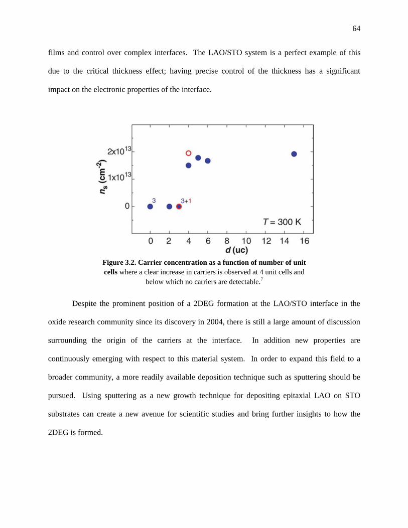
64
films and control over complex interfaces. The LAO/STO system is a perfect example of this
due to the critical thickness effect; having precise control of the thickness has a significant
impact on the electronic properties of the interface.
Despite the prominent position of a 2DEG formation at the LAO/STO interface in the
oxide research community since its discovery in 2004, there is still a large amount of discussion
surrounding the origin of the carriers at the interface. In addition new properties are
continuously emerging with respect to this material system. In order to expand this field to a
broader community, a more readily available deposition technique such as sputtering should be
pursued. Using sputtering as a new growth technique for depositing epitaxial LAO on STO
substrates can create a new avenue for scientific studies and bring further insights to how the
2DEG is formed.
Figure 3.2. Carrier concentration as a function of number of unit
cells where a clear increase in carriers is observed at 4 unit cells and
below which no carriers are detectable.7

65
As previously mentioned, work has already been done with a focus on creating devices
using the LAO/STO system12
and in addition to this it has been shown that the 2DEG can be
formed when both STO and LAO are grown on Si substrates13
demonstrating that the LAO/STO
interface can be incorporated into current industrial platforms and has technological relevance.
However, in order for these devices to be broadly applicable they need to be integrated with
current fabrication technology—most notably there is a need to deposit these thin films
uniformly on large wafers. 90° off-axis sputtering is a scalable process that has been shown to
create smooth, epitaxial films that are uniform over a large area.14,15
This is essential for
integration with silicon. While several groups have grown LAO/STO heterostructures by sputter
deposition,16,17
none have reported a conducting interfacial 2DEG. This task requires finely
tuned growth parameters that avoid having the bulk substrate conducting and the entire sample
insulating, while maintaining a 2DEG at the interface.
Here, we report on the steps necessary for the creation of a 2DEG at the LaAlO3/SrTiO3
heterointerfaces grown by 90° off-axis sputtering.4 The objective is to show the electrical
transport properties of the LaAlO3/SrTiO3 heterointerfaces grown by sputtering are comparable
to those grown by pulsed laser deposition. This would indicate that sputtering can be a viable
alternative to the typical PLD growth of these interfaces. Demonstrating room-temperature
conductive-atomic force microscope switching of 2DEG nanostructures would further show that
functional applications of this material system are extended to the scalable growth technique of
sputtering.

66
3.2. Film growth and structural characterization
In order to create an oxide interfacial 2DEG, we use a different regime of growth
conditions, deviating from the previously reported 3:4 O2:Ar ratio16,18
and high pressure O2
sputter environments.17
In the case of PLD, it has been shown that too high (greater than 7.5
mTorr),19
or too low (less than 7.5 x 10⁻⁷
mTorr)20
oxygen pressure can degrade LAO structural
quality and inhibit 2DEG formation. Even though oxygen vacancies are known to be removed
during post-annealing after LAO growth, earlier works have shown that low oxygen partial
pressure can play a major role in the creation of a 2DEG.21,6,22
However, duplicating the 10-4
–
10-6
Torr21
O2 partial pressures used in PLD can be challenging in sputtering due to typically
higher Ar gas pressure (i.e. 200 mTorr) used for 90° off-axis sputtering. There is a 3-5 order of
magnitude difference in partial pressures between Ar and O2, and pressure in this regime cannot
easily be controlled accurately.
We overcome this difficulty by sputtering in pure Ar and relying on the sputtered single
crystal LAO target to sustain a large enough background pressure of O2 and atomic oxygen to
create an environment similar to PLD. During sputtering of an oxide target material, a relatively
large amount of O2 and more importantly atomic oxygen is produced. The nearly zero activation
energy associated with atomic oxygen compared with the non-zero energy of molecular oxygen23
significantly increases the effective PO2 during sputter growth compared with PLD where only
molecular oxygen is present. This mechanism creates an environment that can produce high
quality 2DEGs2,24
during sputtering while only introducing Ar gas.
Our growth system consists of a 2 inch RF magnetron sputter source in a 90° off-axis
geometry with reference to the sample heater. All films discussed here were grown on TiO2-
terminated (001) STO substrates.5 A LAO/STO control sample was grown by PLD using

67
conditions reported elsewhere.13
Currently pulsed laser deposition (PLD)2,21
is the dominant
deposition technique used for creating oxide interfacial 2DEG heterostructures, and only more
recently has molecular beam epitaxy (MBE)25,26
been used to create a 2DEG. Both of these
growth techniques take advantage of reflection high-energy electron diffraction (RHEED) as an
in situ diagnostic tool, enabling layer by layer control at the unit cell level.8-11
As such, a PLD
grown sample was used as a control. The sputtered samples were grown from a 2-inch single
crystal LAO target mounted on a US Gun II sputter source at an RF power of 50 W. The sample
temperature was 780 °C during growth, consistent with previously reported works.21
A partial
pressure 200 mTorr of Ar was used, with a minimum pre-sputter time of 15 minutes in order to
stabilize a background partial pressure of O2 (and atomic oxygen) produced from the target. This
is a vital step in the growth process as films grown without this extended pre-sputtering were
found to be insulating. It should also be noted that samples we grow at higher PO2, for example
3:4 of O2:Ar, produce insulating films as well. We subsequently annealed the sample for 1 hour
in 300 Torr O2 at 600 °C to ensure that the bulk substrate was not conducting.27
We have utilized x-ray reflectivity as a thickness calibration; this is essential since the
thickness of LAO directly modifies the electronic characteristics of the LAO/STO interface.7 At
the deposition conditions described above, we are able to grow LAO films at a rate of 1.65
Å/min as determined by fitting x-ray reflectivity data as shown in Figure 3.3a. This data also
indicates that the film is smooth with small roughness.

68
Further x-ray analysis shown in Figures 3.3b-d confirms the high-quality epitaxial growth
of the LAO thin films. These high-resolution x-ray diffraction results from a 40 nm sample
(Figures 3.3b-c) show an out-of-plane lattice parameter of 3.74 Å (Figure 3.3b) and in plane
lattice parameter of 3.89Å. This is close to the 3.905 Å STO in-plane lattice constant of the
substrate, leading to a 2.3% tensile strain in the film, referenced to a bulk LAO lattice constant of
3.790Å. This indicates that even at 40nm the film is almost fully strained. The azimuthal phi
scan in Figure 3.3c shows 4-fold symmetry of the LAO film with an in-plane (101) FWHM of
0.26° indicating a very small in-plane mosaic spread of the film while the in-plane FWHM of the
Figure 3.3. Structural characterization of the LAO/STO heterostructure. a) x-ray
reflectivity measurement of the LAO/STO heterostructure displaying clear thickness
plateaus closely matching the model. b) Wide range two theta-omega scan showing
single crystal LAO grown on a STO substrate. c) In-plane (101) phi scan showing 4-
fold symmetry. d) Reciprocal space map of a 10 unit cell sample showing the LAO film
to be fully coherent.
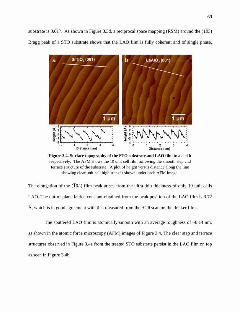
69
substrate is 0.01°. As shown in Figure 3.3d, a reciprocal space mapping (RSM) around the (1̅03)
Bragg peak of a STO substrate shows that the LAO film is fully coherent and of single phase.
The elongation of the (1̅0L) film peak arises from the ultra-thin thickness of only 10 unit cells
LAO. The out-of-plane lattice constant obtained from the peak position of the LAO film is 3.72
Å, which is in good agreement with that measured from the θ-2θ scan on the thicker film.
The sputtered LAO film is atomically smooth with an average roughness of ~0.14 nm,
as shown in the atomic force microscopy (AFM) images of Figure 3.4. The clear step and terrace
structures observed in Figure 3.4a from the treated STO substrate persist in the LAO film on top
as seen in Figure 3.4b.
Figure 3.4. Surface topography of the STO substrate and LAO film in a and b
respectively. The AFM shows the 10 unit cell film following the smooth step and
terrace structure of the substrate. A plot of height versus distance along the line
showing clear unit cell high steps is shown under each AFM image.

70
3.3. Electric characterization
A study of the carrier concentration (ns) as a function of thickness was carried out to show
the existence of a critical thickness. Samples were wire bonded with Al wires in the four-point
van der Pauw geometry and measured Hall coefficients were found to be linear as a function of
applied magnetic field. Figure 3.5a shows a clear transition between a conducting state and an
insulating state at 4 unit cells, consistent with findings on PLD-grown films.7 There can also be
seen a negligible thickness dependence for thicknesses greater than 4 unit cells. This is a clear
Figure 3.5. Transport properties of the sputtered LAO/STO heterostructure. a) The carrier
concentration (ns) as a function of LAO film thickness. Plot of b) carrier concentration (ns), c) mobility
(μH), and d) sheet resistance (RS) as a function of temperature of a 10 unit cell sputter sample compared
with a PLD sample. Blue dashed lines in b) represent power law fits to the mobility above 75 K.

71
indication that these LAO/STO samples produced by sputtering exhibit a 2DEG behavior as
explained by electronic reconstruction.
Additionally, transport measurements were carried out as a function of temperature on both
sputtering and PLD samples with similar growth conditions for comparison with LAO
thicknesses of 10 unit cells in the sputtered sample. The carrier density in the sputtered sample
was found to have a somewhat weaker dependence on temperature than the PLD grown sample
(Figure 3.5b). The temperature dependence of the Hall mobility (μH) is similar above 75 K,
where both obey a power law behavior of T-α
, with α = 2.3 and 2.4 for the sputtered and PLD
grown sample respectively (Figure 3.5c), consistent with reported behaviors.20,24
At low
temperatures the mobility in the sputtered sample saturates at lower values compared with the
PLD grown sample, suggesting increased scattering at these growth conditions. The increased
low-temperature sheet resistance (Rs) is consistent with the reduced mobility values since the
variation in carrier density is small in this range; in the range above 50 K both samples display
similar metallic behavior (Figure 3.5d).
We also demonstrate room-temperature conductive-AFM (c-AFM) switching of 2DEG
nanostructures formed at LAO/STO heterointerfaces grown by 90° off-axis sputtering. The
ability to write and erase nanostructures in these samples has been observed at a range of
thicknesses between 3 and 3.7 unit cells. After 90° off-axis sputtering growth, electrically
conducting contacts to the interface are defined by optical lithography. Then the sample is
prepared by initially milling 25 nm deep trenches through the LAO layer via an Ar-ion mill and
then filling them with 4 nm of Ti followed by 25 nm of Au to form bilayer electrodes via
sputtering. Within the 30 μm × 30 μm “canvas” defined by the electrical contacts, nanostructures
are written and erased at the interface using c-AFM lithography at room temperature. The

72
conductance between two electrical contacts is continuously monitored by a lock-in amplifier
(Figure 3.6a, b). Figure 3.6 shows a typical c-AFM writing and erasing process in a 3.4 unit cell
LAO/STO sample with an initially insulating interface. To begin with, two rectangular pads are
“written” (that is, raster scanning by a Vwrite= +10 V biased AFM tip) for better contacting to the
two Au electrodes, then a conductive nanowire is created by the +10 V biased AFM tip scanning
from one electrode to another at 300 nm/s speed (Figure 3.6a). When the tip reaches the other
electrode, a pronounced and abrupt conductance jump is observed (Figure 3.6c). The observed
Figure 3.6. Room-temperature conductive-AFM (c-AFM) switching of sputtered LAO/STO.
a) Schematic diagram of the writing process. AFM tip is +10V biased. b) Schematic diagram of
the erasing process. AFM tip is -10V biased and moving perpendicularly across the nanowire. c)
Conductance between the two electrodes during the writing process. When the tip reaches the
second electrode, conductance increases abruptly. d) Conductance between the two electrodes
during the erasing process. As the tip scans across the nanowire, conductance decreases to zero.
The red curve shows the best fit indicating a nanowire thickness of 9.2 nm.

73
maximum conductance change and non-exponential decay in atmosphere conditions are
comparable with the 3.4 unit cell LAO/STO samples grown by PLD.12
After writing the nanowire, the AFM tip is repositioned and biased at Verase= -10 V, then
moving perpendicularly across the nanowire at 10 nm/s speed (Figure 3.6b). The conductance
decreased abruptly to zero when the tip reaches the nanowire (Figure 3.6d). The nanowire width
can be qualified by fitting the conductance drop curve with the function G(x) = G0-G1tanh(x/h),12
the red curve in Figure 3.6d. From the best fitting parameters we get a nanowire width of 9.2
nm. The ability to create conductive nanostructures is important for technological applications,
but it also serves as a sensitive probe of the uniformity of the 2DEG. A single insulating patch
along the nanowire is sufficient to prevent conductivity. Here, the properties are comparable to
PLD-grown heterostructures.12
3.4. Conclusions
Sputtering is a thin film growth technique capable of the uniform large area deposition
required for scaling. In this work we have demonstrated that sputtering can be used to grow high
quality epitaxial LaAlO3 films with excellent surface quality on TiO2-terminated SrTiO3
substrates. Growth conditions were chosen in attempt to mimic those used by growth processes
known to form a 2DEG at the interface, and this resulted in the creation of an LaAlO3/SrTiO3
two-dimensional electron gas made by sputtering. We showed that these samples have
comparable electronic transport properties to heterostructures grown with pulsed laser
deposition. We have also demonstrated room-temperature conductive-AFM switching of these
2DEG nanostructures showing the capability to make interesting oxide devices on these films.

74
In summary, we have created another avenue of exploration for the study of the 2DEG at the
LaAlO3/SrTiO3 interface by developing a growth process using a sputter deposition method.
3.5. References
1 Mannhart, J. & Schlom, D. G. Oxide Interfaces—An Opportunity for Electronics.
Science 327, 1607-1611, doi:10.1126/science.1181862 (2010).
2 Ohtomo, A. & Hwang, H. Y. A high-mobility electron gas at the LaAlO3/SrTiO3
heterointerface. Nature 427, 423-426, doi:10.1038/nature02308 (2004).
3 Ohtomo, A., Muller, D. A., Grazul, J. L. & Hwang, H. Y. Artificial charge-modulationin
atomic-scale perovskite titanate superlattices. Nature 419, 378-380,
doi:10.1038/nature00977 (2002).
4 Podkaminer, J. P. et al. Creation of a two-dimensional electron gas and conductivity
switching of nanowires at the LaAlO3/SrTiO3 interface grown by 90° off-axis sputtering.
Applied Physics Letters 103, 071604, doi:10.1063/1.4817921 (2013).
5 Kawasaki, M. et al. Atomic Control of the SrTiO3 Crystal Surface. Science 266, 1540-
1542, doi:10.1126/science.266.5190.1540 (1994).
6 Nakagawa, N., Hwang, H. Y. & Muller, D. A. Why some interfaces cannot be sharp. Nat
Mater 5, 204-209, doi:10.1038/nmat1569 (2006).
7 Thiel, S., Hammerl, G., Schmehl, A., Schneider, C. W. & Mannhart, J. Tunable quasi-
two-dimensional electron gases in oxide heterostructures. Science 313, 1942-1945,
doi:10.1126/science.1131091 (2006).

75
8 Wood, C. E. C. & Joyce, B. A. Tin‐doping effects in GaAs films grown by molecular
beam epitaxy. Journal of Applied Physics 49, 4854-4861, doi:10.1063/1.325517 (1978).
9 Harris, J. J., Joyce, B. A. & Dobson, P. J. Oscillations in the Surface-Structure of Sn-
Doped Gaas during Growth by Mbe. Surface Science 103, L90-L96, doi:10.1016/0039-
6028(81)90091-1 (1981).
10 Bozovic, I. & Eckstein, J. N. Analysis of Growing Films of Complex Oxides by Rheed.
MRS Bulletin 20, 32-38, doi:10.1557/S0883769400044870 (1995).
11 Rijnders, G. J. H. M., Koster, G., Blank, D. H. A. & Rogalla, H. In situ monitoring during
pulsed laser deposition of complex oxides using reflection high energy electron
diffraction under high oxygen pressure. Applied Physics Letters 70, 1888-1890,
doi:10.1063/1.118687 (1997).
12 Cen, C., Thiel, S., Mannhart, J. & Levy, J. Oxide Nanoelectronics on Demand. Science
323, 1026-1030, doi:10.1126/science.1168294 (2009).
13 Park, J. W. et al. Creation of a two-dimensional electron gas at an oxide interface on
silicon. Nat Commun 1, 94, doi:10.1038/ncomms1096 (2010).
14 Eom, C. B. et al. In situ grown YBa2Cu3O7- thin films from single-target magnetron
sputtering. Applied Physics Letters 55, 595-597 (1989).
15 Eom, C. B., Marshall, A. F., Laderman, S. S., Jacowitz, R. D. & Geballe, T. H. Epitaxial
and Smooth Films of a-Axis YBa2Cu3O7. Science 249, 1549-1552,
doi:10.1126/science.249.4976.1549 (1990).
16 Lee, A. E. et al. Epitaxially grown sputtered LaAlO3 films. Applied Physics Letters 57,
2019-2021 (1990).

76
17 Dildar, I. M. et al. Conductivity of LaAlO3/SrTiO3 Interfaces made by Sputter
Deposition. CORD Conference Proceedings (2011).
18 Sader, E., Schmidt, H., Hradil, K. & Wersing, W. Rf-Magnetron Sputtered Lanthanum
Aluminate Buffer Layers on Silicon. Supercond Sci Tech 4, 371-373, doi:10.1088/0953-
2048/4/8/010 (1991).
19 Maurice, J.-L. et al. Electron energy loss spectroscopy determination of Ti oxidation state
at the (001) LaAIO3 /SrTiO3 interface as a function of LaAIO3 growth conditions. EPL
(Europhysics Letters) 82, 17003 (2008).
20 Kalabukhov, A. et al. Effect of oxygen vacancies in the SrTiO3 substrate on the electrical
properties of the LaAlO3 / SrTiO3 interface. Physical Review B 75, 121404 (2007).
21 Huijben, M. et al. Structure-Property Relation of SrTiO3/LaAlO3Interfaces. Advanced
Materials 21, 1665-1677, doi:10.1002/adma.200801448 (2009).
22 Reyren, N. et al. Superconducting interfaces between insulating oxides. Science 317,
1196-1199, doi:10.1126/science.1146006 (2007).
23 Yamamoto, K. et al. Role of Atomic Oxygen Produced by an Electron-Cyclotron
Resonance Plasma in the Oxidation of Yba2Cu3O7-X Thin-Films Studied by Insitu
Resistivity Measurement. Applied Physics Letters 57, 1936-1938, doi:10.1063/1.104147
(1990).
24 Huijben, M. et al. Structure-Property Relation of SrTiO3/LaAlO3 Interfaces. Advanced
Materials 21, 1665-1677, doi:10.1002/adma.200801448 (2009).
25 Jeffrey Gardner, H. et al. Enhancement of superconductivity by a parallel magnetic field
in two-dimensional superconductors. Nat Phys 7, 895-900, doi:10.1038/nphys2075
(2011).

77
26 Warusawithana, M. P. et al. LaAlO3 stoichiometry is key to electron liquid formation at
LaAlO3/SrTiO3 interfaces. Nat Commun 4, 2351, doi:10.1038/ncomms3351 (2013).
27 Moos, R., Menesklou, W. & Hardtl, K. H. Hall-Mobility of Undoped N-Type Conducting
Strontium-Titanate Single-Crystals between 19-K and 1373-K. Appl. Phys. A-Mater. Sci.
Process. 61, 389-395, doi:10.1007/Bf01540113 (1995).

78
4. In situ RHEED during oxide sputtering
4.1. Introduction
As the oxide field progresses, atomic layer controlled growth is becoming ever more
essential for the understanding and engineering of these complex oxide heterointerfaces. This
includes the understanding and manipulation of surfaces and interfaces. Currently, molecular
beam epitaxy (MBE) and pulsed laser deposition (PLD) techniques take advantage of reflection
high-energy electron diffraction (RHEED) as an in situ diagnostic tool of the structure of the
surface during deposition, enabling layer-by-layer control at the unit cell and sub unit cell level.1-
5 The observation of intensity oscillations of the RHEED specular reflection in MBE growth of
semiconductors has been exploited for many years to control stoichiometry and growth rate.1-3
The primary advantage of incorporating RHEED analysis to the growth of artificially layered
superlattices is the precise thickness control of each layer.6 The RHEED technique was readily
adapted to growth of complex oxides with MBE4 because the pressure during growth is
sufficiently low (<10–6
Torr) to avoid scattering of the electron beam and damage to the filament
in the electron source. Subsequently, RHEED at high oxygen pressures (<0.3 Torr) was
developed for PLD by Rijnders et al5 and has been widely adopted for growing epitaxial oxide
films and controlling complex interfaces by this technique.
The development of in situ RHEED analysis for sputter growth would introduce similar
advantages – for example, rapid optimization of growth parameters and control of growth rates,

79
and enhance reproducibility of interface and superlattice growth – to this widely used and
technologically important deposition technique.7-11
Moreover, analysis of in situ RHEED
intensities can provide fundamental information on epitaxial growth mechanisms (e.g. Stranski-
Krastanov, Frank-van der Merwe or Volmer-Weber modes12,13
and layer-by-layer versus step
flow) that is currently unknown for many thin film systems deposited by the sputter technique.
The concept behind layer-by-layer control by RHEED oscillations can be seen clearly in
Figure 1.6. As discussed in Chapter 1, the intensity of the RHEED specular spot is in direct
correlation to the percent of total coverage on a layer.14
When there is complete coverage the
intensity is at a maximum, and when there is only fifty percent coverage the intensity is at a
minimum due to scattering of the electron beam from a rough surface. Following this idea,
RHEED intensity versus time can be used to precisely control the number of unit cells deposited
during layer by layer growth. Beyond this, RHEED provides real time information regarding the
crystallinity, surface roughness as well as many other surface features.
This type of control becomes especially important in the LAO/STO system when
considering the ability to write and erase nanowires on the samples as first reported by Cen et al
in 2009.15
Here, they reported on using a conductive Atomic Force Microscopy (AFM) tip to
effectively “draw” conducting nanowires into the LAO/STO interface. This is only possible
when your films are very thin and below the critical thickness, then by applying a bias, an
additional field is generated in order to induce carrier movement to the interface causing the
interface to locally become conducting. We demonstrated this read and write ability in the
previous section with our sputter grown films but would have benefitted from the use of RHEED
during sputtering.

80
4.2. RHEED with magnetron sputtering
Sputter deposition is a widely used growth technique for a large range of technologically
important material systems. Phase-pure and smooth epitaxial films of carbides,16
nitrides,17,18
oxides,7,19,20
metals,21,22
and more can be deposited by sputtering, from the research level up to
an industrial scale. As increased attention is given to design of emergent phenomena at
interfaces between these materials systems, atomic-layer controlled growth of epitaxial thin films
and artificially layered superlattices has become critical. Despite the many advantages of sputter
deposition, it suffers from a lack of available in situ analysis techniques for atomic-layer control
during growth. Reflection high-energy electron diffraction (RHEED) is generally used to
monitor thin film deposition yet it has not been commonly used during sputtering. This is largely
due to large magnetic fields from the sputter sources that strongly deviate the RHEED beam
trajectory. Additionally, typically high pressures of oxygen and argon associated with sputter
deposition of epitaxial complex oxides (>100 mTorr) can cause the electron beam to scatter
creating a large diffuse background of the intensity and reducing the overall detection range.
The goal of this work is to expand the functionality of this important in situ analysis
technique beyond MBE and PLD by applying it to sputter deposition. In this thesis we solve the
magnetic field problem by presenting a novel approach to minimize or eliminate the influence of
magnet fields in a wide range of growth geometries. The prediction and modeling of the
magnetic field effect on the electron beam is the focus of the following chapter while this chapter
will be more dedicated to the observed magnetic field effect, the gas effect, and mostly on the
use of RHEED in real-time during sputtering.

81
In this chapter we demonstrate digital control of magnetron sputter deposition using in situ
high-pressure RHEED by applying this technique to the widely studied model oxide system,
SrRuO3 (SRO). During 90° off-axis sputtering of SRO films we observed strong specular spot
oscillations. This allows us to identify the growth mode as layer by layer and establishes our
ability to have unit cell control during sputter growth for the first time. Similar results are
observed and presented during the growth of perovskites La0.7Sr0.3MnO3 (LSMO) and LaAlO3
(LAO), confirming that this approach can be universally applied to sputter deposition of other
materials.
4.2.1. Scattering due to gas
As previously mentioned, this use of RHEED with sputtering is very challenging due to
the strong magnetic fields and the high partial pressures of Ar and other process gases present
during the deposition. Both of these have undesirable impacts on the electron beam used for
RHEED. The presence of process gas can scatter a significant portion of the electron beam.
This effect increases the overall background signal observed on the RHEED signal which
decreases the overall dynamic range that can be measured. In this section we aim to demonstrate
the effects of the variable gas environments and demonstrate how the sputter gas environment
differs from that of a typical oxide PLD environment and how that difference affects the RHEED
pattern. Following this we will provide some insight into ways to limit the effects from the
process gas and improve the measureable RHEED pattern.
Both PLD and sputtering have been reported to have working pressures that cover a huge
range of gas pressures, in particular PLD can go from UHV to hundreds of mTorr whereas the

82
lower limit for sputtering is several mTorr due to the need to have atomic collisions in order to
form a plasma. For 90° off-axis sputtering, gas pressures are typically in the hundreds of mTorr
range in order to reduce the number of high energy particles that reach the substrate by
shortening the mean free path and increasing the number of collisions. Sputtering
characteristically uses an inert gas as the sputter species (Ar, Kr, etc.), so as to not react with the
target material, most common of which is argon. For oxide growth a reactive sputter process is
commonly employed by introducing oxygen with argon to ensure the films are fully oxygenated.
The ratio of argon to oxygen can vary dramatically but typically includes some amount of argon.
Contrarily, oxide PLD growth often has no use for a process gas such as argon and as such only
varies the pressure of oxygen to change the plume dynamics and oxidation state.
While the effect of total partial pressure on the RHEED signal is trivially known, higher
pressures lead to an increased number of scattering events between the electron beam and the
gas, the effect of the gas species is low commonly considered. For this we consider the
difference between the differential scattering cross section between argon and oxygen. This
takes into account the Bohr radius for each element and the electron beam energy in order to
quantify the amount of scattering given a specific incidence angle. For this we can first consider
a fairly typical RHEED energy of 20 keV and then simulate23
and compare the scattering cross
section between argon and oxygen as shown in Figure 4.1. What is clearly evident is that the
differential scattering cross section for argon is approximately 4 times larger than that of oxygen
demonstrating that the amount of the electron beam that we will be scattered is 4 times larger and
this remains approximately true up to very large scattering angles. This has a major impact when
comparing sputtering with PLD with regards to the effect on the RHEED beam. From this

83
calculation we can expect to observe a much larger amount of diffuse scattering during
sputtering due to the presence of argon gas, increasing the overall background intensity.
From these simulations we can then begin to consider ways to reduce the overall
scattering caused by the gas. Since we are limited in the number of variables this is very
straightforward but none the less something that is important to consider and rarely discussed in
the literature related to high pressure RHEED. By increasing the electron energy from 20 keV to
35 keV which is the upper limit of our power supply, we can see a noticeable decrease in the
scattering cross section starting around 1 degree of theta or the incidence angle as shown in
Figure 4.1.23
The decrease in the number of scattering events that occur at greater than 1 degree
is significant and as such we will be work at 35 keV for the remained of the thesis. This increase
in the electron energy does have consequences which need to be taken in account as well. The
higher energy results in an enlarged Ewald’s sphere and thereby contracting the diffraction
pattern as observed on the phosphor screen. This may not be a negative impact depending on the
Figure 4.1. The differential scattering cross section for Ar and O atoms are shown as a
function of theta. The scattering cross section is shown for both 20 and 30 keV electron energies
for each atom type. It can be seen that Ar has a significantly larger scattering cross section than
oxygen and that higher electron energies help reduce the scattering at higher angles.23

84
overall RHEED setup but should be known as it can lead to a decrease in resolution, the number
of discernable pixels between diffraction spots.
In reality we can observe these calculated effects with the most noticeable change coming
when the gas species is varied. For this experiment the total pressure in the chamber was fixed at
75 mTorr, the RHEED power supply was also held constant at 35 keV including the filament
current, grid, and focus parameters. The only variable that was changed was the gas species in
the chamber so as to observe a direct comparison. This effect is seen in Figure 4.2 where the
change from an oxygen gas species to argon species is observed by capturing a diffraction
pattern from a SrTiO3 substrate near room temperature. Both images show a sharp diffraction
pattern typical of a high quality STO substrate. What is noticeably difference is the overall
brightness of the patterns. The pattern captured in the oxygen environment appears dimmer
when compared with the one from the argon environment. This can be understood as the
majority of the diffraction intensity is focused in the spots where the camera is saturated and very
little of the beam intensity is observed as diffuse scattering. Conversely, the image taken in the
Figure 4.2. Scattering comparison for Ar and O2 gas. A RHEED pattern of a STO substrate is
shown in a and b in oxygen and argon environments respectively. The diffuse background intensity
is noticeably larger in the argon environment as predicted by argons larger scattering cross section.

85
argon environment is very bright with measurable intensity in nearly every pixel shown. This is
a result of the higher scattering cross section of argon, scattering the electron beam in all
directions from the diffraction pattern.
The consequences of this effect are that the measurable dynamic range decreases due to
the effective minimum value increasing from 0 to a nonzero value. As an example, when
monitoring intensity oscillations, one can imagine a scenario where the actual minimum intensity
is a lower value than the background intensity in which case a significant amount of diffuse noise
would be measured in this situation rather than a smooth curve. Additionally, the background
intensity becomes more significant as the total pressure increases. Two possible remedies for
this issue are to increase the electron energy as previously mentioned but also to reduce the
working distance of the electron beam so as to limit the number of scattering events that occur.
For this work 35 keV was used and a total working distance from electron gun aperture to
phosphor screen of 20 cm although shorter distances are recommended keeping in mind that both
of these adjustments make a contraction in the pattern spacing.
4.2.2. Deflection due to magnetic field
The effect on the electron beam stemming from the scattering due to gas is significant
and deserves attention but the effect from stray magnetic fields is a much larger issue. This is
such an important issue that in fact an entire chapter of this thesis is dedicated to the handling of
the fields produced by the sputter sources. Knowing that a more in depth treatment of this topic
will be presented later on, in this section it will suffice to outline the premise of the issue and
ways to deal with it at a very basic level.

86
As with any instance where a focused electron beam is used, great care is taken to the
shield the apparatus from stray magnetic fields as they can deflect the beam in unpredictable
ways. In particular with regards to our RHEED setup, the electron gun is completely wrapped
with μ-metal to shield from undesired magnetic fields. μ-metal is a nickel-iron alloy that has
very high magnetic permeability and works by reshaping the magnetic field lines to that of shield
so that they go around the apparatus. In addition to the electron gun being magnetically shielded,
the extension tube inside the chamber is also shielded in μ-metal. In this way only the area
where the electron beam is exposed is it susceptible to external magnetic fields.
Typically the primary sources for stray magnetic fields are electromagnetic motors, DC
currents, permanent magnets (i.e. the full range vacuum gauge), and the geomagnetic field.
While these fields exist everywhere they are often manageable for RHEED systems and do not
pose a significant problem. The issue when discussing RHEED with sputtering is that
magnetron sputter sources by definition have very strong permanent magnets in them with
magnetic moments on the order of several thousand Gauss. The importance of these magnets,
one center cylindrical magnet and an outer annular magnet, for the sputter process was
previously discussed in Chapter 1. The crux of the issue is that in order to use RHEED during
sputtering these strong magnets must be placed in close proximity during 90° off-axis sputtering
to the section of the exposed electron beam which results in significant deflection of the beam
trajectory.
The degree to which the beam is deflected and the new trajectory path is dependent on
relative orientation and position of the sputter sources to the beam, the number of sources, the
sizes of the sputter sources, and the working distance of the electron beam. All of these degrees

87
of freedom make this a complex problem to solve in simple terms and as such finite element
modeling has been employed to model our system and the electron beam trajectory for several
common growth geometries. This is the focus of the following chapter where we present these
simulations and also discuss novel ways to mitigate the deflection.
For this chapter it is enough to acknowledge that this is a serious problem and that for the
in situ characterization discussed later in this chapter the magnetic field was dealt with through
the large amount of flexibility and degrees of freedom that were built into the growth chamber
originally for other purposes. A schematic of the growth chamber and deposition setup is seen in
Figure 4.3 which highlights the 90° off axis geometry, the relative RHEED arrangement and
some of the important degrees of freedom used to counter the deflection of the electron beam.
The general procedure for aligning the electron beam is as follows; we begin with the magnetron
sputter source pulled away from the electron beam as far as possible to avoid major deflections.
Then, as it is inserted into the chamber we are able to track the deflection of the electron beam
and correct for the deflection as best as possible while still maintaining a diffraction pattern.
This requires adjustments of azimuthal angle, tilt angle, and also repositioning of the electron
gun using the X-Y translation stage. As best as possible the XYZ heater manipulation stage is
not adjusted so as to maintain the same growth working distances. This procedure is done in
small steps and is a slow process taking upwards of an hour to complete. If the sputter source is
quickly introduced into the chamber to the final growth position the electron beam will bend so
severely that it will no longer be viewable on the screen at which point it is very challenging to
find again.

88
Using all of the degrees of freedom at our disposal we are able to keep the electron beam
on the very edge of the screen but we are at our limit for our standard growth position. Any
more significant bending and we would not be able to recover the pattern on the screen. Once in
the growth position we are still able to observe a diffraction pattern from an STO substrate but
the pattern is severely tilted and the diffraction spots are no longer sharp but are streaky. This is
demonstrated in Figure 4.4 where a comparison between a STO pattern without a field and one
with the magnetron sputter sources is shown. Additionally a RHEED image is shown at the
Figure 4.3. Schematic of the growth chamber demonstrating the relative orientation between the
heater and the sputter gun is shown along with the RHEED setup. Required degrees of freedom of
the heater and electron gun are shown as the tilt and azimuth and the x, y, and beam tilt, respectively.

89
growth pressure demonstrating the combination of the magnetic field and scattering due to gas.
However, this result is adequate because the most important factor is that we can observe and
monitor the pattern in particular the specular spot which we are able in this geometry. This
means that we are able to proceed with the growth of oxide materials while in situ monitoring
with RHEED.
4.3. RHEED intensity oscillations
Despite the fact that to this point we have not solved the issue of the beam deflection due
to the magnetron sputter sources we are able to observe a RHEED diffraction patter at the growth
pressure and with a single sputter source in the growth position as schematically shown in Figure
4.3. This means that the specular spot intensity can then be monitored in real time during the
sputter growth with the only a few remaining questions. First, how does the electric field
Figure 4.4. Sputter deposition effects on RHEED. A STO substrate in vacuum is shown in a with sharp
diffraction spots and Kikuchi lines. The effect from the magnetron sputter source on the diffraction
pattern is seen in b, where the pattern is clearly tilted the diffracted spots are less sharp and the Kikuchi
lines disappear. c shows the tilted RHEED pattern with the addition of 200 mTorr of Ar gas where a large
diffuse intensity obscures the pattern further.

90
produced by the sputter power supply and the plasma itself affect the electron beam and
observed intensity on the screen? Second, what is the growth mode of oxide films grown by 90°
off-axis sputtering? The later question will be addressed thoroughly in the remainder of this
chapter through the deposition of three separate well studied oxide materials; LAO, LSMO, and
SRO. The first two materials, LAO and LSMO, are known to grow in the layer by layer mode
during PLD growth with clear RHEED oscillations observed.24-26
SRO growth on the other
hand, has been well established to grow primarily in the step flow regime following the first few
unit cells.27,28
These materials will help address the way in which sputter deposition is similar or
different to PLD and if it possible to observe RHEED oscillations during sputter deposition.
However, before continuing on to the actual depositions and RHEED analysis, the first
question will be addressed. Typical of most oxide sputter growths, an RF power generator was
used for these growths to avoid charging on the target surface. Despite the oscillating potential
of the sputter source there is still a noticeable effect when the plasma is struck. It has not been
studied to a great degree but the intensity of the specular spot occasionally does not change, has a
sharp increase in intensity, or a sharp decrease. We believe this is a product of the electron beam
being shifted very slightly when the sputter voltage is turned on and the initial alignment of the
electron beam on the sample. Such that when the electron beam is shifted slightly as a result of
the electric field the incidence angle changes rapidly and depending on the initial alignment it
can increase or decrease the intensity. This does not however appear to be a significant effect on
the resulting intensity monitoring since it is a one-time event then stabilizes and is not a major
change in the overall intensity.

91
The sputter plasma itself is full of ionized elements and free electrons by definition.
Additionally, the plasma is relatively large from a 2” sputter source and the deposition of the
target material happens everywhere. This can have a serious negative impact on the phosphor
screen. If care is not taken to protect the screen from the sputter plasma it will not only light up
as a result of the free electrons striking the screen but it will also become coated rather quickly
and become unusable. To solve this problem an aluminum foil cone with a small aperture, ~1”
or less, was formed and placed over the screen. The aperture was placed as close as possible to
the substrate such that the electron beam could diffract off of the substrate and then travel freely
to the phosphor screen inside of the cone. This greatly reduced the line of sight deposition from
the sputter source and the overall interaction between plasma and the screen since the conduction
through the smaller aperture is poor. With the added cone, degradation of the phosphor screen
has not been noticed after tens of sputter depositions, while without the cone a change can be
noticed after the first deposition. This may not be the perfect solution but the point of this
discussion is to make it clear that the interaction between the phosphor screen and the plasma
cannot be ignored and this is the best solution we were able to find. With this problem solved we
can now turn to the monitoring of sputter deposition with real time RHEED.
4.3.1. LaAlO3/SrTiO3

92
As discussed in the previous chapter, the LAO/STO system is an ideal model
heterostructure for in situ RHEED with sputtering due to the high quality epitaxial growth that
we demonstrated by sputtering29
and the strong electrical dependence on the thickness.30
With
this in mind we chose this material system to be the first growth we monitored by RHEED with
the hope of observing layer-by-layer intensity oscillations. Due to the lack of real time analysis
techniques during sputtering, it was unclear what to expect in terms of growth mode.
In Figure 4.4c the starting RHEED pattern of the TiO2 terminated STO substrate is shown
at the growth conditions as previously discussed. The background intensity and tilting of the
pattern is clearly visible. Despite the poor signal to noise ratio the pattern is present and during
Figure 4.5. RHEED oscillations during a LaAlO3 growth on a SrTiO3 substrate showing
specular spot intensity oscillations that get weak very quickly but then are maintained out to greater
than 10 oscillations. The inset shows a zoomed in region to better display the oscillations with low
intensity. The large amount of noise is a result of the diffuse scattering from Ar gas screening the
low intensity RHEED pattern shown where the spots are barely observable above the background.

93
the deposition the specular spot and the diffracted spot intensities were monitored. The resulting
intensity versus time is shown in Figure 4.5, where intensity oscillations can be seen from both
the specular spot and diffracted spot out to greater than 15 oscillations. This clearly establishes
that RHEED oscillations can be observed during sputtering for the first time and that sputter
deposition can proceed in an extended layer-by-layer fashion, at the very least for LAO growth
on STO. The specular spot and diffracted spot intensities oscillate out of phase which is
commonly observed31
and they have a period of 49 seconds. The data is rather noisy and the
intensity dampens quickly after the first few oscillations. This dampening is fairly frequently
observed by other groups,30,32
suggesting that the sputtered LAO growth dynamics are
comparable to the PLD grown films. Following the dampening the intensity stabilizes and the
oscillation amplitude is just large enough to appear above the noise level. When considering the
static RHEED image shown in Figure 4.5 from the mid-zone where the intensity of the spots are
barely above the background noise it can be understood how the recorded amplitude would be
weak in comparison to the noise level. None the less, RHEED oscillations were reproducible
during sputter growth of LAO films confirming that RHEED with sputtering is promising as a
reliable in situ analysis technique that has been greatly needed during sputter deposition.
To confirm precisely that each of these RHEED oscillations are in fact stemming from
one unit cell of deposition in the layer-by-layer regime, an ex situ XRR measurement was
performed as seen in Figure 4.6a. From the fit performed of the XRR measurement an accurate
thickness of 11.4 nm can be obtained. Using this thickness, the total deposition time of 1500 s,
and the out of plane lattice parameter, the unit cell deposition rate can be calculated to compare
with the RHEED oscillation period. The out of plane 2θ – θ scan is shown in Figure 4.6b where

94
the (002) film and substrate peaks are shown. This gives an accurate out-of-plane lattice
parameter of 3.74 Å for the LAO film which is important for the calibration since this value can
vary as stoichiometry and the strain state change. The unit cell deposition rate obtained from the
thickness, time, and c - lattice parameter is 49 s/uc which matches closely with what was
obtained by the RHEED analysis confirming that the RHEED oscillations do in fact correspond
to one unit cell of growth. With this real time information it would then be possible to accurately
control the thickness of the film and thus the conductive state of the interface using RHEED.
Figure 4.6. Ex situ structural and surface analysis of the LAO/STO film. An XRR measurement
is shown in a with the corresponding simulation used to get an accurate film thickness. The out of
plane XRD measurement in b of the LAO film grown on STO indicates an c-lattice parameter of 3.74
Å which is used to form a growth rate calibration. The AFM image seen in c shows the LAO film has
smooth step and terrace structure similar to the substrate.

95
Ex situ analysis was further carried out on this film with AFM shown in Figure 4.6c. The
surface of the film is comparable to the surface shown in the previous chapter with an rms
roughness of 0.15 nm. Additionally, the rocking curve of the out of plane 002 peak is shown
with a FWHM of 0.08° which is also comparable to what was previously shown. This
information further supports what is determined with the in situ RHEED by the images taken
after the deposition which show clear sharp spots indicative of a high quality crystalline material
and a very smooth surface. This demonstrates that a lot of information about the film can be
obtained in situ without ever exposing the film to air and performing time consuming ex situ
measurements.
4.3.2. La0.7Sr0.3MnO3/SrTiO3
The RHEED data taken on the LAO films was a good starting point as it was the first
demonstration of the RHEED oscillations during a sputter grown film. However, the data was
very noisy throughout and the oscillations had small amplitudes and not well defined out to a
large number of periods. It was determined that a large portion of this noise was due to external
vibrations and noise entering the system by vibrating both the electron gun as well as the heater
mount among other places. To avoid this noise and improve the signal a number of steps were
taken to isolate the chamber from the external vibrations. Additionally, the sampling density of
the RHEED pattern was reduced and thereby increased the averaging time for each data point.
The capture rate is still fast enough to capture 3 frames per second so as to not miss any fine

96
details in the RHEED signal. By taking these measures the signal to noise ratio was significantly
improved.
To further prove the robustness of the RHEED with sputtering technique we chose to
grow LSMO films of STO substrates. This material system was chosen for several reasons; not
only is it a widely studied material system also with a critical thickness26
but also because it is
known to show strong RHEED oscillations when grown by PLD.25,26
In this way we could grow
a relevant material system that is known to grow layer by layer with PLD and also one that will
hopefully bring the signal level of the RHEED oscillations well above the nose level although
the scattering from the gas will still be present.
Figure 4.7. La0.7Sr0.3MnO3 growth on a SrTiO3 substrate showing clear RHEED
intensity oscillations indicating a layer-by-layer growth mode. The inset shows a
diffraction pattern of the film after growth in vacuum with the magnetic field present,
sharp spots with some streaking is seen indicating a flat 2-dimensional surface.

97
The LSMO films were grown at 750 °C in a 200 mTorr gas environment of 34:1 sccm of
Ar to O2 from a stoichiometric ceramic LSMO target. Films grown at 135 mTorr, with the same
gas ratio as above, also exhibited similar results (not shown here). The films were grown with an
RF power of 50 W in the 90° off-axis geometry. The fact that LSMO is a magnetic material, the
presence of the target further complicates the bending of the electron beam in addition to the
magnetron sputter source.
Despite this added field the initial RHEED pattern from the STO substrate matches
closely to what was previously shown with the clear tilting of the pattern. Monitoring the
specular spot intensity during the LSMO growth gives the resulting RHEED oscillations as can
be seen in Figure 4.7. The inset in Figure 4.7 shows a diffraction pattern of the LSMO film after
the growth in vacuum where sharp spots can be seen with some minor streaking indicating a very
flat 2-dimensional surface and good crystalline quality. The RHEED intensity data from the
(0,0) specular spot versus time for the LSMO growth is a clear improvement from the LAO
growth, with strong oscillations that decay with time which is very similar to previously reported
PLD growth of LSMO.26
Once again this suggests that the LSMO growth dynamics are very
similar when comparing PLD to sputtering. This also indicates that layer by layer growth by
sputtering is not specific to just one material system and is probably quite robust.
In order to characterize the structure and surface of the LSMO film grown on STO, x-
ray diffraction (XRD), x-ray reflectivity (XRR), and atomic force microscopy (AFM)
measurements were carried as seen in Figure 4.8. The out-of-plane XRD plot seen in Figure 4.8a
shows the substrate and film (002) peaks. The film peak has clear Kiessig Fringes indicating the
surface and interface are very smooth and sharp. The rocking curve of the LSMO film (002)

98
peak in Figure 4.8b has a FWHM value of 0.026° which is on the order of the STO substrate and
indicates high epitaxial crystalline quality.
In Figure 4.8c the XRR of the LSMO film on STO is seen with a fit which shows good
agreement. From the XRR data and the fit we can get a very accurate measurement of the film
thickness and also insights into the surface and interface quality. From the XRR thickness
calibration we find a growth rate of 32 s/uc. This matches very well with the RHEED
oscillations which also show an average period of 32 s/uc. However, a closer look shows that
Figure 4.8. X-ray and AFM measurements of the LSMO film. a) Out of plan 2θ-θ scan showing
the LSMO and substrate (002) peak with clear Kiessig fringes. b) Rocking curve of the LSMO (002)
film peak with a FWHM of 0.026°. c) XRR scan of the heterostructure used for thickness calibration
from the simulation. d) AFM image of the LSMO film showing clear step and terrace structure.

99
the period starts slightly dilated during the first 6 unit cells before finding its steady state growth
rate. The far less noisy data for the LSMO in comparison to the LAO data permitted us to obtain
this finer level of analysis. This demonstrates the power of RHEED to have careful layer by
layer control to a finer degree than can be achieved by a calibration and timed growth especially
when very thin films are desired. Figure 4.8d shows the AFM image of the film which clearly
shows the step and terrace structure preserved in the film from the treated STO substrate. This
confirms the smooth surface as expected from the RHEED pattern, the Kiessig Fringes and the
XRR fit.
4.3.3. SrRuO3/SrTiO3
The LSMO film growth confirmed that the sputter with RHEED technique is in fact quite
robust and likely applicable to any material system that can grow in the layer by layer regime.
To further test the robustness of this technique we turned to SRO growth which is commonly
believed to grow in a step flow regime.27,32
While intensity oscillations are a characteristic sign
of layer by layer growth, step flow growth has a RHEED signature of no oscillations and simply
a continuous bright intensity. The PLD grown SRO films typically start in the layer by layer
regime before transitioning to step flow after the first few unit cells.27
This makes the SRO
materials system a very interesting one to observe by RHEED during sputter deposition since
epitaxial SRO films were first deposited by sputtering7 and it is commonly assumed that they
also adopt the same growth mode as observed in PLD. This assumption is made due to the lack
of in situ analysis options available during sputtering. SRO is also an important material system

100
as it is commonly used as an epitaxial bottom electrode in oxide heterostructures due to SRO’s
excellent lattice match with many common substrates.
We grow SRO thin films on TiO2 terminated STO substrates in the 90° off-axis geometry
with in situ RHEED. The sputtered SRO films were grown at 590 °C with a working pressure of
200 mTorr. The gas ratio for this growth was 12:8 Ar to O2 respectively and the RF power was
fixed at 100 W. Using in situ RHEED we can identify both the growth mode and observe
RHEED oscillations during the deposition as seen in Figure 4.9a. The intensity of the (0,0)
specular spot was monitored as a function of time during the deposition. Figure 4.9a clearly
shows that the film grows in the layer by layer mode with oscillations that extend out to greater
than 50 clear intensity oscillations, each corresponding to a single unit cell of deposition (only
shown out to 40 here to be able to distinguish peaks). This allows for the ability to have exact
unit cell control of the growth during sputter deposition, which has never previously been
demonstrated for SRO growth out to more than ~10 unit cells and never during sputter growth.
Figure 4.9. RHEED oscillations from SRO growth are seen in a) as the black line. The oscillations
are shown out to 40 unit cells with the red line showing the fit. The inset highlights the first few unit
cells where the extended period can be seen. b) is a plot of the period versus unit cell displaying the
relaxation time required to reach the approximate steady state with an exponential decay fit in red.

101
Furthermore, the extended oscillations are of particular interest when comparing the
sputter grown SRO to that which is observed in PLD grown SRO. In PLD grown films, it has
been shown that the growth mode of SRO begins as layer by layer growth and transitions to step
flow growth after several unit cells.27
In addition, these PLD grown films show a RHEED
signature corresponding to the transition from RuO2 termination to SrO termination.33
We find
that this change in termination can also be observed in sputter grown SRO films, as seen in
Figure 4.9a and made clearer in the inset. The elongated first unit cell oscillation of
approximately 38 seconds is nearly double the steady state average of 19.3 seconds per unit cell
and corresponds to the transition from BO2 termination to AO termination. However, in contrast
to PLD growth, the SRO does not transition from layer by layer to step flow growth. Figure 4.9a
shows RHEED oscillations characteristic of layer by layer growth with each oscillation
corresponding to one unit cell. If the growth mode were to have transitioned to step flow, the
oscillations would have died out. The oscillations were observed out to greater than 50 unit
cells, clearly establishing the ability to have layer by layer control over sputter grown SRO films.
Due to the transition in growth mode of PLD grown SRO, layer-by-layer control out to many
unit cells has not been demonstrated, giving sputtering better thickness control over SRO films.
To further demonstrate the capability of this technique, these films were grown without
presputtering in order to observe the time necessary to reach steady state. A fit of the oscillations
is shown in red in Figure 4.9a starting with the first complete peak. This fit was used to obtain
the crest to crest period of each oscillation, or the time required for each successive unit cell,
which is plotted in Figure 4.9b. From this plot it can be observed that unit cell growth rate starts
near 21 seconds per unit cell and relaxes down to the steady state period of approximately 19.3

102
seconds after 15 unit cells following approximately an exponential decay shown by the red
curve. From this we can determine the minimum presputter time but can also observe that it is a
non-uniform growth rate throughout, indicating that without the use of an in situ monitoring
technique precise unit cell control may not be possible.
Figure 4.10. Topographic and structural characterization of the SRO film by AFM, XRD, and
XRR. (a) AFM image of the SRO surface showing single unit cell steps and incomplete step edges.
The inset shows the RHEED image of the SRO with sharp spots after the growth in vacuum with the
sputter source in position causing the tilting of the pattern. (b) Out of plane XRD scan showing the
relationship between the (002) peak of the SRO and STO. Distinct Kiessig fringes are present
indicating the interface and surface are both sharp and smooth. (c) The XRR data shown in black with
the fitted data in red provide an accurate thickness estimation, and indicate the high quality of the
surface and interface. The fit gives an estimated total thickness of 27.1nm.

103
The RHEED image of the 27.1 nm SRO film after the growth is seen in the inset of
Figure 4.10a. This image is taken in vacuum with the magnetic field from the sputter source still
present, which is evident by the tilted pattern. Clear diffracted and specular spots can be
observed with minimal streaking suggesting high crystallinity and a predominantly two-
dimensional surface. Ex situ analysis of the SRO film structure and thickness is carried out with
x-ray diffraction (XRD) and x-ray reflectivity (XRR) respectively and the surface morphology is
characterized by atomic force microscopy (AFM), as seen in Figure 4.10. The AFM image in
Figure 4.10a shows clear terrace structures; however, the steps do not have linear and smooth
edges, and show some small single unit cell islands on the terraces. This is comparable to SRO
films grown on STO by PLD,33
but the existence of the small islands on the sputter grown film
may be an indication of nucleation sites corresponding to the layer by layer growth as opposed to
the step flow growth of PLD. The AFM result also corroborates observations from the RHEED
pattern that the film surface is very smooth.
The out-of-plane XRD scan seen in Figure 4.10b shows the relationship of the (002) SRO
film peak to the STO (002) substrate peak. Clear Kiessig Fringes can be seen, which indicate a
smooth surface and interface. The rocking curve of the (002) SRO peak has a FWHM of 0.024°
indicating low mosaic spread and high crystalline quality. These ex situ measurements confirm
what has already been observed in situ with RHEED, demonstrating the power and efficiency of
real time monitoring.
The XRR data and corresponding fit can be seen in Figure 4.10c with the raw data in
black and the fitted data in red. Using the fit, an accurate total thickness of the film is found to
be 27.1 nm from which a growth rate of 20.1 seconds per unit cell is derived. When compared to

104
the 19.3 seconds per unit cell steady state rate acquired from the RHEED oscillations it can be
seen that these results are in close agreement. However, from the varying period of the
oscillations seen in Figure 4.9b it is clear that using RHEED is a more robust and reliable way of
ensuring precise unit cell control compared with a time based calibration. Additionally, these
results confirm that the SRO grows in a layer by layer mode because one would expect these
values to be significantly different if there was also a step flow contribution to the growth. This
is a clear indication that each RHEED oscillation corresponds to exactly one unit cell being
deposited on the sample surface, and as such, is the first demonstration by any growth method of
greater than 50 RHEED oscillations providing digital control during SRO growth.
4.4. Conclusions
This chapter clearly establishes the difficulty associated with RHEED during sputtering
and likely the reason to why the use of RHEED as a real time monitor is not more prevalently
observed during sputter deposition. The scattering due to the gas has been clearly demonstrated
for both oxygen and argon gas and ways to diminish the scattering effect have been laid out. For
this chapter it was sufficient to acknowledge the magnetic field existed and ways to deal with it
through flexibility without actually solving the issue. The magnetic field issue will be further
addressed in the following chapter through simulations of the field and the effect it has on the
electron beam. Despite the challenges we demonstrate that the RHEED pattern from the
substrate can be observed in the 90° off-axis sputter conditions. It naturally follows then that the
intensity versus time can be recorded from the pattern during sputter deposition which was

105
demonstrated in this chapter for LAO, LSMO, and SRO growth. All three of these scientifically
relevant materials demonstrate layer by layer growth which is of particular interest for the SRO
growth. With these results we can clearly say that digital control of sputter growth by in situ
RHEED is possible creating a new avenue for real time analysis during sputtering which
otherwise did not readily exist.
4.5. Reference for chapter 4
1 Wood, C. E. C. & Joyce, B. A. Tin‐doping effects in GaAs films grown by molecular
beam epitaxy. Journal of Applied Physics 49, 4854-4861, doi:10.1063/1.325517 (1978).
2 Harris, J. J., Joyce, B. A. & Dobson, P. J. Oscillations in the Surface-Structure of Sn-
Doped Gaas during Growth by Mbe. Surface Science 103, L90-L96, doi:10.1016/0039-
6028(81)90091-1 (1981).
3 Braun, W. Applied RHEED: reflection high-energy electron diffraction during crystal
growth. (Springer Science & Business Media, 1999).
4 Bozovic, I. & Eckstein, J. N. Analysis of Growing Films of Complex Oxides by Rheed.
MRS Bulletin 20, 32-38, doi:10.1557/S0883769400044870 (1995).
5 Rijnders, G. J. H. M., Koster, G., Blank, D. H. A. & Rogalla, H. In situ monitoring during
pulsed laser deposition of complex oxides using reflection high energy electron
diffraction under high oxygen pressure. Applied Physics Letters 70, 1888-1890,
doi:10.1063/1.118687 (1997).

106
6 Nie, Y. F. et al. Atomically precise interfaces from non-stoichiometric deposition. Nat.
Comm. 5, 4530, doi:10.1038/ncomms5530 (2014).
7 Eom, C. B. et al. Single-Crystal Epitaxial Thin Films of the Isotropic Metallic Oxides Sr1-
xCaxRuO3 (0 ≤ x ≤ 1). Science 258, 1766-1769, doi:10.1126/science.258.5089.1766
(1992).
8 Tybell, T., Ahn, C. H. & Triscone, J. M. Ferroelectricity in thin perovskite films. Applied
Physics Letters 75, 856-858, doi:10.1063/1.124536 (1999).
9 Lin, A. et al. Epitaxial growth of Pb(Zr0.2Ti0.8)O3 on Si and its nanoscale piezoelectric
properties. Applied Physics Letters 78, 2034, doi:10.1063/1.1358848 (2001).
10 Gibert, M., Zubko, P., Scherwitzl, R., Iniguez, J. & Triscone, J. M. Exchange bias in
LaNiO3-LaMnO3 superlattices. Nat Mater 11, 195-198, doi:10.1038/nmat3224 (2012).
11 Peters, B. et al. Epitaxial films of Heusler compound Co2FeAl0.5Si0.5 with high crystalline
quality grown by off-axis sputtering. Applied Physics Letters 103, 162404,
doi:10.1063/1.4825338 (2013).
12 Venables, J. A., Spiller, G. D. T. & Hanbucken, M. Nucleation and Growth of Thin-
Films. Reports on Progress in Physics 47, 399-459, doi:10.1088/0034-4885/47/4/002
(1984).
13 Venables, J. A. Introduction to Surface and Thin Film Processes. (Cambridge University
Press, 2000).
14 Ohring, M. in Materials Science of Thin Films (Second Edition) (ed Milton Ohring)
417-494 (Academic Press, 2002).

107
15 Cen, C., Thiel, S., Mannhart, J. & Levy, J. Oxide Nanoelectronics on Demand. Science
323, 1026-1030, doi:10.1126/science.1168294 (2009).
16 Jansson, U. et al. Low temperature epitaxial growth of metal carbides using fullerenes.
Surf Coat Tech 142, 817-822, doi:10.1016/S0257-8972(01)01111-2 (2001).
17 Singh, P. et al. Growth and characterization of GaN thin films by magnetron sputter
epitaxy. J Vac Sci Technol A 16, 786-789, doi:10.1116/1.581059 (1998).
18 Quintela, C. X. et al. Epitaxial CrN thin films with high thermoelectric figure of merit.
Adv Mater 27, 3032-3037, doi:10.1002/adma.201500110 (2015).
19 Eom, C. B., Marshall, A. F., Laderman, S. S., Jacowitz, R. D. & Geballe, T. H. Epitaxial
and Smooth Films of a-Axis YBa2Cu3O7. Science 249, 1549-1552,
doi:10.1126/science.249.4976.1549 (1990).
20 Eom, C. B. et al. In situ grown YBa2Cu3O7- thin films from single-target magnetron
sputtering. Applied Physics Letters 55, 595-597 (1989).
21 Harp, G. R. & Parkin, S. S. P. Epitaxial growth of metals by sputter deposition. Thin
Solid Films 288, 315-324, doi:10.1016/S0040-6090(96)08808-6 (1996).
22 Oh, S. et al. Epitaxial growth of rhenium with sputtering. Thin Solid Films 496, 389-394,
doi:10.1016/j.tsf.2005.09.091 (2006).
23 Jablonski, A., Salvat, F. and Powell, C. J. NIST Electron Elastic-Scattering Cross-Section
Database. Vol. Version 3.2, SRD 64 (National Institute of Standards and Technology,
2010).
24 Ohtomo, A. & Hwang, H. Y. A high-mobility electron gas at the LaAlO3/SrTiO3
heterointerface. Nature 427, 423-426, doi:10.1038/nature02308 (2004).

108
25 Izumi, M. et al. Atomically defined epitaxy and physical properties of strained
La0.6Sr0.4MnO3 films. Applied Physics Letters 73, 2497-2499, doi:10.1063/1.122494
(1998).
26 Huijben, M. et al. Critical thickness and orbital ordering in ultrathin La0.7Sr0.3MnO3.
Physical Review B 78, 094413, doi:10.1103/Physrevb.78.094413 (2008).
27 Choi, J., Eom, C. B., Rijnders, G., Rogalla, H. & Blank, D. H. A. Growth mode transition
from layer by layer to step flow during the growth of heteroepitaxial SrRuO3 on (001)
SrTiO3. Applied Physics Letters 79, 1447-1449, doi:10.1063/1.1389837 (2001).
28 Koster, G. et al. Structure, physical properties, and applications of SrRuO3 thin films.
Reviews of Modern Physics 84, 253-298, doi:10.1103/RevModPhys.84.253 (2012).
29 Podkaminer, J. P. et al. Creation of a two-dimensional electron gas and conductivity
switching of nanowires at the LaAlO3/SrTiO3 interface grown by 90° off-axis sputtering.
Applied Physics Letters 103, 071604, doi:10.1063/1.4817921 (2013).
30 Thiel, S., Hammerl, G., Schmehl, A., Schneider, C. W. & Mannhart, J. Tunable quasi-
two-dimensional electron gases in oxide heterostructures. Science 313, 1942-1945,
doi:10.1126/science.1131091 (2006).
31 Haeni, J. H., Theis, C. D. & Schlom, D. G. RHEED intensity oscillations for the
stoichiometric growth of SrTiO3 thin films by reactive molecular beam epitaxy. Journal
of Electroceramics 4, 385-391, doi:10.1023/A:1009947517710 (2000).
32 Huijben, M. et al. Structure-Property Relation of SrTiO3/LaAlO3 Interfaces. Advanced
Materials 21, 1665-1677, doi:10.1002/adma.200801448 (2009).

109
33 Rijnders, G., Blank, D. H. A., Choi, J. & Eom, C. B. Enhanced surface diffusion through
termination conversion during epitaxial SrRuO3 growth. Applied Physics Letters 84, 505-
507, doi:10.1063/1.1640472 (2004).

110
5. Finite element modeling
5.1. Introduction
Throughout this thesis the theme of combining RHEED with sputter deposition is ever
present. Along with this theme is the notion that one of the limiting factors for combining these
processes together is the presence of strong permanent magnets in the sputter sources.
Previously, groups have acknowledged that this is an issue but since they had such a large
working distance it was not a significant factor.1 In our own work we have also experienced this
issue but were able to accommodate the bending of the electron beam through large degrees of
freedom which are not always sufficient. One easy solution may be to sputter without the
magnets which is possible yet extremely uncommon. However, the purpose of this chapter is to
not only understand the effect of the magnets on the electron beam but to find a robust solution
where RHEED with magnetron sputtering can be utilized in a large range of growth geometries.
To this point we have demonstrated that not only is RHEED an extremely powerful and
useful in situ analysis tool but also that critical information can be obtained from monitoring the
RHEED pattern during sputtering, such as unit cell oscillations. In order to take this one step
further and predict the effect of the magnetic field on the electron beam trajectory, COMSOL
(COMSOL Multiphysics® version 5, AC/DC and Particle Tracing Modules) was used to create a
finite element model of the magnetic field produced by the magnets in a 2-inch planar magnetron

111
sputter gun oriented in the 90° off-axis geometry, and to simulate the beam trajectory when
passing through the magnetic field. The finite element method is a useful strategy that solves
complex partial differential equations which collectively describe the entire system.2 The domain
of the problem is divided into a group of subdomains with each subdomain represented by a set
of element equations that locally approximate the original equations for the problem.
Recombining these local solutions into a single global solution yields accurate results for the
solution of the problem.
Finite element analysis (FEA) is a computational tool which utilizes the finite element
method. FEA includes the use of meshes which are generated in order to divide a complex
problem into small elements. Generally, more complex areas require finer meshes resulting in
smaller local elements and a larger amount of computing power. Once the object of interest is
discretized, the correct material properties and boundary conditions are applied to each small
element. These small elements are then used to solve the global problem. COMSOL
Multiphysics is a powerful tool capable of simulating complex physical systems. COMSOL uses
FEA and partial differential equations techniques to accurately simulate physical systems input
by the user.
The core COMSOL program enables simulations of mechanics, and additional modules
are available to expand the range of possible simulations. For this work, COMSOL core as well
as the ACDC modules and particle tracing module were used. The ACDC module allowed for
the simulation of a magnetic field produced by permanent magnets and the particle tracing
module allowed for the simulation of an electron beam as it moves through the magnetic field.

112
5.2. Modeling parameters
The object geometries were created in SolidWorks to scale and then imported into
COMSOL. The electron gun, phosphor screen, and heater were simulated as Type 316 steel, with
relative permeability of 1. The magnets were modeled with a relative permeability of 1.05 based
on NdFeB rare earth magnets and a remnant flux density of 1.201 T. All of the remaining
volume was simulated as a low pressure gas with relative permeability of 1. The particles in the
beam were given the mass and charge of an electron, and 25 particles were released from a 1 mm
wide aperture (exaggerated from actual dimensions slightly to make more obvious) with a
velocity of 1.05 x 10⁸ m/s corresponding to 35 keV of kinetic energy.
The particle beam experienced a magnetic force from the magnets once the particles were
released. A mesh was created for the entire geometry and then a time dependent study was
performed. Post processing included coloring the north and south ends of each magnet red and
blue respectively as well as all the objects to easily distinguish them. Three-dimensional images
were produced showing the beam path via colors corresponding to the magnetic force exerted on
the beam at each point. A two-dimensional vector field showing the magnetic field strength and
direction was also created. After post processing, camera views were chosen to export the proper
images for use as figures.
5.3. Single and two gun 90° off-axis geometries

113
We simulated many magnetic orientations within several different geometries in order to
predict the bending of the beam and to find an optimal geometry for minimal beam deflection
caused by the strong magnetic fields present. The ideal magnetic field for our purposes would be
parallel with the electron beam’s direction which would result in zero deflection. The next best
solution is one in which the field strength along the beam path is reduced and the field direction
is constant for the entirety of the trajectory. This would reduce the magnitude of the deflection
and also make the deflection more predictable as it would be uniaxial. In particular, magnetic
fields that are perpendicular to the electron beam and horizontal will push the beam only
vertically, still allowing much control to overcome the problems caused by the deflection of the
beam. This concept is the basis of our findings and will be elucidated more clearly in this
section.
The first model created was representative of the growth geometry used for the previous
growths, one sputter gun in the 90° off-axis geometry, such that a better understanding of the
deflection we observed could be obtained. Subsequently we modelled a two gun 90° off-axis
geometry with facing guns to enable the growth of heterostructures and ideally balance the field.
A 2-dimensional cross-sectional view of the simulated magnetic vector field distributions can be
seen in Figure 5.1. The cross-section is a slice through a plane containing the heater and sputter
sources, with the electron gun positioned out of the plane of the page and the phosphor screen
into the plane of the page such that the electrons travel into the page. All of the working
distances used for these simulations are to-scale representations of our actual chamber setup.
Figure 5.1a shows the magnetic field close to the sample for the simplest case of a single gun in
the off-axis geometry. Here we can note the relative field strength and additionally the direction

114
of the field lines close to the sample. In the single gun setup the field lines point close to vertical
with some tilt toward the magnets.
If we consider an electron beam traveling straight into the page at the point directly above
the center of the sample in Figure 5.1a, the Lorentz force will point perpendicular to the
magnetic field direction toward the magnets with a magnitude proportional to the magnetic field
strength. Consequently, the beam will bend laterally in the x-direction towards the magnets at
this point. Similarly, COMSOL can be used to explore more complex chamber geometries. In
Figure 5.1b, a two-gun off-axis setup is shown with two sets of symmetrically facing magnets
(“symmetric” setup). In the cross section, an increase in the field strength near the sample is
observed along with a significantly transformed overall vector field distribution. Despite these
Figure 5.1. 2-dimensional cross-sections showing the magnetic field close to the sample for the single
gun, two gun symmetric and two gun antisymmetric magnet polarities. The electron beam direction
is into the page, and the RHEED phosphor screen is behind this plane (into the page). (a) Single gun off-
axis geometry shows the magnetic field lines close to the sample are pointing nearly vertically resulting in
a predominantly lateral Lorentz force. (b) Two gun symmetric off-axis geometry with the field lines
close to the sample completely vertical. (c) Two gun antisymmetric geometry displays the magnetic field
lines close to the sample are horizontal resulting in a Lorentz force in the y-direction. The magnitude of
the magnetic field can also be compared between the three setups.

115
considerable changes, the Lorentz force near the sample has similar results to that of the single
gun simulation with the force pointing completely laterally in the x-direction, now with a larger
magnitude.
In Figure 5.1c, the same two-gun facing geometry is shown as in Figure 5.1b except in
this case the magnet orientation of one gun is inverted such that the two guns are now in an
“antisymmetric” setup. In this setup, once again a change in the magnetic field lines is seen as
well but in this geometry the strength of the field near the sample is reduced. Most notably, the
magnetic field direction at the sample now points horizontally and the resulting Lorentz force
near the sample points downward in the y-direction. This significant change in the magnitude
and direction from both the single gun geometry and the “symmetric” setup renders the
“antisymmetric” geometry more desirable from a practical point of view (see discussion below).
The 2-dimensional cross sections of the magnetic field distribution shown in Figure 5.1
are a good starting point for understanding the field strength and orientation near the sample
surface and qualitatively predicting the electron beam deflection in different chamber
geometries. However, the 2-dimesional plots make the assumption that the beam is traveling
straight into the plane and do not consider the field in 3-dimensions. To quantitatively predict
the electron beam path a time-resolved finite element simulation is required, as provided by the
combination of the AC/DC and Particle Tracing modules in COMSOL. Simulations can be made
in COMSOL that use actual working distances between the electron gun, phosphor screen, heater
block, and magnets in the sputter source in our chamber geometry, including the 35 kV beam
voltage used experimentally, and can also simulate hypothetical setups. This provides a useful
platform for understanding what is observed and also for predicting and designing future

116
systems.
Figure 5.2. Finite element simulations showing electron beam deflection in single gun, symmetric,
and antisymmetric sputter source geometries and their resulting RHEED patterns. (a) Single off-
axis sputter source layout with from a top view showing a clear deflection in the x direction is observed
with the beam missing the edge of the phosphor screen. (b) Two opposite facing sputter guns in the
symmetric geometry from a top view showing a more dramatic bending of the beam than in (a). (c)
Antisymmetric geometry is shown resulting in moderate bending only in the y direction and striking the
phosphor screen. The RHEED pattern seen in (d) is the image of a bare STO substrate in vacuum with a
single sputter source in the off-axis position. Clear tilting of the pattern is observed as well as a reduction
in the sharpness of the diffracted spots. (e) A RHEED image from an STO substrate is shown for the
antisymmetric setup exhibiting no tilting of the pattern and sharp specular and diffracted spots.

117
Figure 5.2a, b, and c show 3-dimensional representations and simulations of the single
gun, symmetric, and antisymmetric setups, respectively. Side views of these simulations can be
seen in Figure 5.3. The color gradient along the beam shows the magnitude of the magnetic field
that the electrons encounter traveling from the gun to the screen. From these simulations the
electron beam path can be predicted for all three cases, providing a more complete understanding
of the influence of the magnetic field along the entire trajectory than the cross sectional views.
Figure 5.2a shows that the deflection due to the magnetic field from a single gun is sufficient for
the beam to completely miss the 55 mm diameter phosphor screen. It can be noted the Lorentz
force from the 2-dimensional cross-section (Figure 5.1a) predicts the beam to bend not only
towards the magnets but also slightly towards the heater. However, following the full trajectory
in 3D the net result is that the beam is actually bent away from the heater.
Figure 5.2b shows the 3D beam trajectory in the symmetric gun setup resulting in a
significantly larger deflection of the beam than observed for the single gun setup. From this, it
can be concluded that using the symmetric gun setup in our chamber would make it more
difficult both to have the beam diffract off the sample and have the resulting pattern strike the
phosphor screen. The large lateral deflections seen in the single gun or symmetric gun
geometries can be eliminated by inverting the magnetic polarity of one gun, as seen in Figure
5.2c for the antisymmetric setup. This geometry has the additional advantage of minimizing the
strength of the magnetic field along the electron beam trajectory (note the predominantly blue
color of the beam and the field strengths indicated by the color scale), resulting in dramatically
lower overall deflection of the beam. Crucially, because the field lines are parallel to the x-
direction along the entire beam path, the beam is only deflected in the y-direction and can easily

118
be made to strike the phosphor screen. Upon a careful analysis of the 3D simulations, the field
lines change direction twice along the beam path leading to two zero-field points where the beam
bends first up and then down again.
Figure 5.3. Finite element simulations side view showing electron beam deflection in (a)
single sputter source, (b) symmetric dual, and (c) antisymmetric dual sputter source
geometries. (a) The single gun geometry is shown where the beam deflects above the surface
of the sample and also misses the screen. In (b), the symmetric setup is simulated which
shows a significant deflection in the -y direction, also resulting in the beam missing the sample
surface. The symmetric setup can be seen in (c) which shows a small bump in the beam
trajectory above the sample but the beam returns to the y=0 starting value at the screen.

119
The presence of two sputter guns in the antisymmetric configuration has additional
benefits beyond permitting the use of RHEED during growth. First, the growth of complex
heterostructures or superlattices of two different materials would require in any case the presence
of two sputter sources. Second, it has been shown that an antisymmetric sputter geometry
improves film uniformity over large areas by eliminating the confined magnetic field created by
a symmetric setup that leads to resputtering of deposited materials; this makes scalability more
feasible.3 These factors all point to the 2-gun antisymmetric geometry as being ideal for
sputtering of complex oxides with in situ RHEED.
Experimentally the results match well with what is predicted from the simulations.
Without making any changes to the system, the direct beam in both the single gun and symmetric
setups is not observed where as in the antisymmetric setup the direct beam strikes the screen.
However, using all of the degrees of freedom in our chamber the beam can be redirected for the
single gun setup such that the beam diffracts off the SrTiO3 (STO) substrate and its diffraction
pattern can be observed on the screen. This pattern is shown in Figure 5.2d where the field
causes the diffraction pattern to noticeably tilt, and the spots become irregularly shaped and the
diffracted spots become very weak. Furthermore, the Kikuchi lines typically seen on a bare
substrate are no longer observable. For the symmetric case, the deflection is so severe that the
degrees of freedom are not enough to redirect the beam onto the screen and no diffraction pattern
is observable. For the antisymmetric setup, very minor adjustments were required in order to
observe a pattern from an STO substrate, shown in Figure 5.2e. There is no tilting present in this
pattern and sharp diffraction and specular spots are observed. The pattern does show some
minor streaking as a result of the magnetic field but strong Kikuchi lines are still present and the

120
pattern is significantly more comparable to a typical STO pattern in the absence of a magnetic
field. This confirms the simulation results that the antisymmetric configuration is the ideal setup
for in situ sputtering with RHEED.
5.4. Two antisymmetric configurations
While the antisymmetric geometry is clearly preferable, further analysis is required to
fully understand the effects of the field on the RHEED pattern. Specifically, we should consider
the fact that there can be two possible configurations of the magnets; configuration A where the
field near the sample points to the left and configuration B where the field points the opposite
direction. This can be achieved by flipping the polarity of all the magnets such that we still have
antisymmetric magnets and the field shape is the same but the direction of the field points in is
opposite. This is shown more clearly in Figure 5.4 where both configurations are displayed. The
obvious change in impact on the electron beam between A and B is the direction of the Lorentz
force is opposite for each. However, what is not immediately obvious is what happens when the
beam is not traveling directly between the sputter sources.
To this point we have been considering an idealized setup where the sputter sources are
perfectly symmetric about the sample and the RHEED setup, and the electron beam travels
perfectly straight between the sputter guns. In reality this can be extremely challenging to
achieve and as such it is worthwhile to consider what happens when the system is varied. At a
basic two-dimensional level, as seen in Figure 5.4a and b, one can consider the Lorentz force not
only directly above the sample but also shifted horizontally for configurations A and B. It can be

121
seen that for configuration A the Lorentz force always points back toward the center regardless
of which side of center the beam starts. Conversely for configuration B the Lorentz force always
has a component that points away from center.
In general this indicates that for configuration A the beam will always be re-centered and
for B the beam will always travel away from center unless starting perfectly centered. To get the
entire picture however, we must once again consider the full three-dimensional view which is
shown in Figure 5.4b. The three-dimensional view does in fact confirm what was originally
assumed as clearly shown by the simulations where the beam starts off-set in both positive and
negative x for both configurations. For A, the beam consistently is forced back to the center of
Figure 5.4. Magnetic field simulations for the two possible antisymmetric configurations are show in
a and b. Configuration A is shown in a while configuration B is shown in b. This effect is further
illustrated in the 3-dimensional models of the beam trajectory where an off-set in the x direction is
deflected back towards the middle for configuration A as seen in c and e, and for configuration B the
beam deflects away from the center in d and f.

122
the screen whereas in B the beam is push away by the Lorentz force. This can have significant
implications when attempting to align the beam and additionally when any off-sets may exist.
Furthermore, at a finer level when only considering the RHEED pattern, configuration A actually
acts to elongate the pattern in the y direction whereas B will force the pattern to seem more
diffuse. Additional studies are needed to further understand the implications of these changes
and to create a more concrete conclusion about which configuration is more desirable, but for
now understanding that the difference exists is important.
5.5. Generic solution
The antisymmetric solution that was found in the previous section for 90° off-axis
sputtering clearly limits the magnitude of the deflection and also restricts the deflection to a
single axis making it more predictable and thus easier to account for. However, the 90° off-axis
geometry is a fairly specific growth geometry that is not necessarily applicable to all materials
systems. Being able to form a more generic rule of thumb that encompasses a much broader
range of growth geometries would therefore be significantly more beneficial for the wide-
ranging sputter community. Additionally, finding a setup where there is virtually zero effect
from the sputter sources would be extremely beneficial.
Using what was previously found in the two gun 90° off-axis setup, additional growth
geometries were simulated. What was found is presented in Figure 5.5, which shows a standard
two gun 45° confocal geometry as well as a setup that includes two sputter guns facing the heater
with the sample between them, occasionally referred to as a high rate off-axis setup.

123
What can clearly be seen in both of these setups in that near sample surface the field lines are
horizontal when the magnets are antisymmetric. While the field strengths here are higher than in
the 90° off-axis setup, the same uniaxial bending as seen previously can be expected. Regardless
of the magnitude of deflection, the uniaxial bending is highly predictable and offsets can easily
be built into a system. It should also be noted that the working distances here are somewhat
random and the magnitude of the magnetic field will understandably scale with the proximity of
the sputter sources to the sample. From these simulations a generic guideline can be formed
which can be applied to a large range of growth geometries. Essentially, as long as two sputter
sources are present in some non on-axis yet geometrically symmetric setup with antisymmetric
magnet arrangement, a uniaxial bending perpendicular to the sample surface can be expected.
This expands the robustness of this technique to include nearly every angle of off-axis growth
and also every angle of confocal growth.
Figure 5.5. Confocal and high rate off-axis antisymmetric setups. Two sputter arrangements are
shown with antisymmetric magnet arrangements for 45° confocal sputtering in a and two gun high rate
off-axis sputtering in b. In both cases the field lines are horizontal above the sample resulting in a
uniaxial deflection of the electron beam.

124
When considering pure on-axis growth, it is desirable to have a solution for this
arrangement as well. Even in on-axis growth, there is a need to balance the field in some way.
At first we considered an antisymmetric sputter source behind the heater facing the main source.
However, this resulted in a non-uniaxial and severe bending of the electron beam. Contrary to
what was previously observed, a symmetric setup was simulated and the two-dimensional
magnetic field cross-section is shown in Figure 5.6. For this model, it is more helpful to consider
the electron beam traveling horizontally directly above the sample. In this case all of the field
lines point horizontally as well and switch orientations at the center point. This results in a net
deflection due to the magnetic field of zero since the resulting Lorentz force is pointing in the
same direction or opposite direction of the beam path.
Figure 5.6. An on-axis sputter arrangement
with symmetric sputter sources centered
around the substrate surface is shown. The
field lines are all perfectly horizontal in this
plane indicating that an electron beam
traveling horizontally would no experience a
Lorentz force.

125
Although it may not be an ideal setup to have another sputter source (or simply another
set of magnets) behind the heater and in certain situations not possible, it is the best arrangement
for completely avoiding deflection due to the sputter source. Furthermore, it is the only setup in
which field lines are parallel to the electron beam that we have found thus far. In addition to
this, one can imagine a situation where the heater can then rotate from one sputter source to the
other to deposit multi-target heterostructures while still incorporating RHEED. This is
reminiscent of the motions described for the hybrid chamber in Chapter 2 except in theory there
would be zero effect from the sputter sources. This setup has not yet been experimentally
demonstrated but it should be noted that a small variation of the electron beam from the central
axis will result in some bending of the beam. This is true for all of our simulations and it is also
worth mentioning that RHEED does require some finite incident angle of the beam on the
sample whereas here we are simulating the beam traveling parallel to the substrate surface.
Nonetheless this clearly demonstrates that not only are we able to form a general rule of thumb
for non on-axis setups but even for on-axis deposition the deflection can be completely avoided.
5.6. Antisymmetric SRO growth
To further demonstrate the power of the antisymmetric setup, SRO thin films were grown
using configuration A. While our current growth chamber does not have the ports needed to
allow the inclusion of two sputter source in the antisymmetric arrangement, we were able to add
a dummy set of magnets to act as if a sputter source was present. For this, a stand was
constructed to hold a set of sputter magnets perfectly opposite the functioning sputter gun with

126
antisymmetric polarities. Oscillations of the RHEED specular spot intensity during the
deposition are readily observable, as shown in Figure 5.7a, and permit the calibration of the
deposition of single unit cells and allow the identification of layer-by-layer growth mode, as
discussed below and previously demonstrated. A Gaussian fit of the oscillations (the red line in
Figure 5.7a) was used to obtain the crest-to-crest period of each oscillation, and a plot of these
periods is shown in Figure 5.7b. After the initial few unit cells, the growth rate is fairly constant
throughout with an average period of 20.7 seconds.
Similar to the previously discussed SRO growth, the STO substrates are treated to form
a TiO2 termination4 prior to growth, and the corresponding atomic force microscopy (AFM)
image exhibits a single unit-cell step-and-terrace structure with nearly straight step edges is
shown in Figure 5.7c. The inset to Figure 5.7c shows the RHEED image of the STO substrate
prior to growth in vacuum; the sharp diffracted and specular spots confirm the high quality
crystalline substrate and smooth surface. The inset in Figure 5.7d shows the RHEED images
taken in vacuum after the SRO growth. The diffraction pattern still shows sharp spots with some
minimal streaking suggesting a high degree of crystallinity in the film and a predominantly two-
dimensional surface. The AFM image in Figure 5.7d shows a clear step-and-terrace structure
with single unit-cell step height and some small single unit cell islands on the terraces. This
morphology is comparable to SRO films grown on STO by PLD,5 but the existence of the small
islands on the sputter grown film may be an indication of nucleation sites corresponding to the
layer by layer growth deduced from the extended RHEED specular spot oscillations. The AFM
result also confirms observations from the RHEED pattern that the film surface is atomically
smooth.

127
The film thickness determined by x-ray reflectivity (XRR) scan confirms that each
RHEED oscillation corresponds to the deposition of a single unit cell as shown in Fig. 4e. The
fit suggests that the surface and interface are smooth and the density is uniform throughout, and
yields a total film thickness of 10.9 nm corresponding to a growth rate of 21.7 seconds per unit
cell. This rate agrees well with the 20.7 seconds per unit cell steady state rate acquired from the
RHEED oscillations in Fig.4b. This confirmation has several implications. First, observation of
RHEED oscillations allows for an in situ, real time capability to control sputter deposition at the
level of a single unit cell. Second, extended RHEED oscillations identify a layer-by-layer
growth mode for SRO by sputtering, unlike step-flow growth mode that characterizes SRO
deposition by PLD after the first few unit cells.6 Third, analysis of the RHEED oscillations at
Figure 5.7. RHEED intensity oscillations during SRO growth and unit cell by unit cell growth rate
plot along with the corresponding AFM and RHEED images. The XRR data for the SRO film is also
shown. (a) Specular spot RHEED oscillations during SRO growth on STO. The actual data is seen in
black with the Gaussian fit in red. Clear oscillations are observed corresponding to one unit cell of
growth. (b) The peak to peak period for each unit cell of growth is shown. The inset highlights the first
few oscillations where the extended period can be seen due to the termination conversion during SRO
growth. (c) AFM image of the STO substrate prior to growth showing smooth step and terrace structure.
The inset shows the RHEED image of the STO substrate in vacuum before growth. (d) AFM image of
the SRO surface showing single unit cell steps and incomplete step edges. The inset shows the RHEED
image of the SRO film with sharp spots after the growth in vacuum and no tilting of the pattern. (e) The
XRR data (black line) and fits (red line) provide an accurate thickness estimation of 10.9 nm, and indicate
the high quality of the surface and interface.

128
the start of growth allows the identification of a surface termination inversion in the first few unit
cells of deposition. As shown more clearly in the inset of Figure 5.7b as the shoulder to the
second peak, the period from the first peak to the shoulder is 1.5 times the steady-state period.
The termination inversion from RuO2 to SrO in the first few unit cells reported here for
sputtering is similar to that reported for SRO growth by PLD.5 However, in contrast to PLD
growth, the SRO does not transition from layer by layer to step flow growth after the termination
inversion. The extended RHEED oscillations that characterize layer-by-layer growth by
sputtering allows real time calibration and control of film thickness to the unit-cell level, as
compared to the time-based calibration required for the step-flow growth mode by PLD.
While these results are very similar to what was previously demonstrated, it should also
be noted that the oscillation amplitude is not as large during the antisymmetric growth as
previously shown for the single gun. Additionally, the oscillations do not extend out to as many
periods as in the single gun setup. This may be a result of the antisymmetric arrangement
affecting the dynamics of the plasma near to the sample surface similar to what Newman et al.
observed.3 This is further supported by the fact that the growth rate is slower for the
antisymmetric setup despite all other parameters being kept constant. Moreover, since there is
no evidence of the film surface roughening by AFM, it could be plausible that the growth is
converting to step flow growth in this regime more readily than observed in the single gun setup.
Nonetheless, this growth confirms that the antisymmetric setup produces an improved RHEED
pattern and also can be used to have layer by layer control during sputtered film growth.

129
5.7. Conclusions
Finite element models were created for a wide range of growth geometries such that the
deflection of the electron beam due to the magnetron sputter sources could be reduced and
mitigated. For the single gun 90º off-axis sputtering setup that was used to grow films in the
previous chapter, the FEA was able to predict a similar bending to what was observed via
experiment. While this is useful for understanding the deflection and even designing setups that
can accommodate this bending the ultimate goal was to determine a way to mitigate or avoid all
deflections. This was accomplished through the addition of a second sputter source which
should have an antisymmetric magnet arrangement with respect to the primary sputter gun for
any non on-axis growth setups. This results in a uniaxial bending that his highly predictable and
greatly reduced from the single gun setup. For on-axis deposition, a magnetically symmetric
sputter gun facing the primary gun behind the heater will result in zero deflection of the electron
beam.
Further work is required to fully understand the effect of the two possible magnetic
configurations in the antisymmetric setup, but clearly there is a difference. Of significant interest
is the difference between the SRO grown via one gun versus the two gun setup. Nominally these
two growths should be the same but clearly the magnetic fields have an effect on the deposition
and this will also require further investigation to get a better grasp on what is happening. Now
that a basic guideline has been established for the inclusion of magnetron sputter deposition with
RHEED this should open the door for many interesting future studies.

130
5.8. References for chapter 5
1 Svedberg, E. B., Birch, J., Edvardsson, C. N. L. & Sundgren, J. E. Real time
measurements of surface growth evolution in magnetron sputtered single crystal Mo/V
superlattices using in situ reflection high energy electron diffraction analysis. Surface
Science 431, 16-25, doi:10.1016/S0039-6028(99)00498-7 (1999).
2 Strang, G. & Fix, G. J. An analysis of the finite element method. Vol. 212 (Prentice-Hall
Englewood Cliffs, NJ, 1973).
3 Newman, N., Cole, B. F., Garrison, S. M., Char, K. & Taber, R. C. Double gun off-axis
sputtering of large area YBa2Cu3O7- superconducting films for microwave applications.
IEEE Transactions on Magnetics 27, 1276-1279, doi:10.1109/20.133417 (1991).
4 Kawasaki, M. et al. Atomic Control of the SrTiO3 Crystal Surface. Science 266, 1540-
1542, doi:10.1126/science.266.5190.1540 (1994).
5 Rijnders, G., Blank, D. H. A., Choi, J. & Eom, C. B. Enhanced surface diffusion through
termination conversion during epitaxial SrRuO3 growth. Applied Physics Letters 84, 505-
507, doi:10.1063/1.1640472 (2004).
6 Choi, J., Eom, C. B., Rijnders, G., Rogalla, H. & Blank, D. H. A. Growth mode transition
from layer by layer to step flow during the growth of heteroepitaxial SrRuO3 on (001)
SrTiO3. Applied Physics Letters 79, 1447-1449, doi:10.1063/1.1389837 (2001).

131
6. Summary and future thoughts
In this thesis, a clear goal was set upon from the start with Richard Feynman’s prediction
guiding the way. The goal of using reflection high energy electron diffraction as a means to
garner atomic level control over film growth was the focus. Although RHEED is a well-
established technique, we attempted to push the commonly accepted bounds and limits to expand
RHEED into the realm of sputter deposition. Sputter deposition is an important thin film process
for a wide range of material systems and yet lacks the clear benefit of in situ diffraction that PLD
and MBE take advantage of through RHEED.
A novel thin film deposition system was designed and constructed to incorporate PLD,
sputtering, and RHEED into one chamber body. This design allowed for an easy switch between
PLD and sputter deposition all while maintaining a diffraction pattern. Using these growth
processes in conjunction with one another allowed for the deposition of complex epitaxial
heterostructures for superconducting quantum bits that included oxides and refractory metals,
which are extremely challenging to deposit via PLD and easily grown via sputtering. The
microwave loss properties of these shunt capacitors are extremely sensitive to the interface states
and as such RHEED was an invaluable tool for monitoring the interfaces in real time throughout
the deposition.

132
While we were able to monitor the surface in real time during the multilayer deposition,
we were not able to observe intensity oscillations during the sputter deposition indicative of layer
by layer growth. To observe this powerful phenomenon during sputtering which is the most
commonly desired feature of real time RHEED analysis, a new material system was sought that
was known to grow layer by layer during PLD and also exhibited a strong thickness dependence.
To accomplish this, LaAlO3 growth was optimized separate from the RHEED chamber and was
shown to have electric properties similar to PLD grown films. This was the first time that a
conducting 2DEG was formed at the LAO/STO interface by sputtering and showed a sharp
transition to the conducting state after 4 unit cells of growth. This laid the ground work for
future studies of layer by layer controlled growth with in situ RHEED.
Once the conducting interface was formed, the LAO growth was moved to the hybrid
chamber where real time RHEED analysis was possible. Despite the scattering due to high
pressures of argon and also the strong deflection of the beam due to the magnetron sputter
source, clear RHEED oscillations were observed during the 90° off-axis LAO growth. This was
the first demonstration of layer by layer controlled growth by RHEED during sputter deposition
that we are aware of. To further improve on this process and also demonstrate the robustness of
the technique, LSMO and SRO films were deposited and both showed clear, large amplitude
intensity oscillations out to greater than 20 unit cells exhibiting the ability to have precise unit
cell control during sputter deposition. Interestingly, this was also the first time that extended
RHEED oscillations (>10) had been observed during SRO growth which is commonly known to
grow in the step flow regime during sputtering. This is something that may have interesting
implications and deserves further investigation in the future.

133
As acknowledged here and in previous works, the magnetic fields produced by the sputter
sources can have a large negative impact on the electron beam used for RHEED analysis.
Depending on the growth setup, the magnetron sputter sources can bend the beam so far that it is
no longer detectable. This was what we observed during the 90° off-axis deposition.
Fortunately, the deposition chamber had sufficient degrees of freedom to accommodate this
deflection and obtain the RHEED pattern back on the phosphor screen. However, this is not a
permanent solution and not a plausible one for all growth geometries. As such, finite element
modeling was used to better predict the deflection of the electron beam and also used as a tool to
design ways of avoiding the massive deflections.
Through the finite element modeling, we were able to predict the deflection we observed
in experiment and proceed to identify a setup that significantly mitigates the deflection and
restricts it to a uniaxial and predictable bending. This is accomplished by adding a second
sputter source to the chamber that is facing the original source. Most importantly, the magnets in
the second sputter source need to be rearranged such that they are oppositely poled to the first
source, antisymmetric, which results in horizontal field lines near the sample surface and a
strictly vertical deflection of the beam. This was then expanded to be applicable to all two gun
setups that have some degree of non on-axis nature to them as long as the sputter sources have
antisymmetric magnetic polarities. Furthermore, for on-axis deposition, a facing sputter source
behind the heater with symmetric polarity is needed to completely reduce the Lorentz force that
the electron beam experiences to zero. In this way, a large portion of sputter geometries are
accounted for and have a clear and straightforward path to mitigating or erasing the deflection of
the RHEED beam due to the magnetron sputter guns.

134
This finding has vast implications, not only for creating a new ability to control film
thicknesses at the unit cell level in real time during sputter deposition, but also for potentially
getting even closer to Feynman’s prediction. Certain areas of material space may be
significantly easier to access through sputter deposition (nitrides, high oxidation states, etc.)
when compared to PLD, MBE, or other techniques. However, these areas may have gone
unexplored thus far due to the lack of necessary in situ tools for fine level control. New types of
superlattices may be possible, with the ability to have unit cell control of the SRO growth for
example, that were not abundantly feasible previously. One area of particular interest may be
moving towards true reactive sputtering with the incorporation of pure metal targets. The
alkaline earth metal oxides, for instance, are typically unstable in air, and as such can be very
difficult to use as target materials. Whereas, strontium metal for instance, can be used as a target
material and through reactive sputtering can form strontium oxide films. Combine this with a
ruthenium target and RHEED, and alternating deposition similar oxide MBE may be possible
where fine control over the layers and stoichiometry is possible. This area has largely been
unexplored. Additionally, higher order phases can be accessed in this way that are metastable
otherwise. This is only one specific example but the options are vast given the uncharted space
that exists due to the lack of a proper real time tool during sputtering, until now.