InTech-The Vertical Cavity Surface Emitting Laser Vcsel and Electrical Access Contribution
29
0 The Vertical-Cavity Surface Emitting Laser (VCSEL) and Electrical Access Contribution Angelique Rissons and Jean-Claude Mollier Institut Superieur de l’Aeronautique et de l’Espace (ISAE), Université de Toulouse France 1. Introduction This chapter aims at highlighting the influence of the electrical access of different kinds of Vertical-Cavity Surface-Emitting Laser (VCSEL) (Rissons & Mollier, 2009). By presenting an overview of electrical equivalent circuit modeling and characterization for the VCSEL chip, based on the Scattering parameters, an overview of the VCSEL performance is given in order to provide a good knowledge of this device behavior in various operation modes and avoid its inadequate utilization (Rissons et al., 2003), (Perchoux et al., 2008), (Bacou et al., 2009). Due to the emergence of the short distance optical communication, the VCSELs have become, in the past ten years, a key component of the optical interconnections. The current progress in the VCSEL technology makes this laser diode promising for different application fields and competitive with respect to the Edge-Emitting laser (EEL) and the Light Emitting Diode (LED) (providing the laser performance while keeping the cost effectiveness of the LED)(Koyama, 2006),(Suematsu & Iga, 2008). Above all the VCSELs have been designed to fulfill the need of optoelectronic circuit planarization. Since its invention in 1977 by Prof. K. Iga (Iga et al., 1988) and its first commercialization at the end of the 90’s, the VCSEL structure finds itself in a state of constant progress. Today, it covers a wide wavelength emission range (from the blue-green band up to the infrared) that enables the usage of these components in various application fields, not only in the short distance digital communications (LAN, Avionic network (Ly et al., 2008), ...) but also in consumer applications (laser printers, laser mice, display systems, etc.). Fig. 1. comparison between Edge Emitting laser (on the left) and VCSEL (on the right) 12 www.intechopen.com
-
Upload
joshua-whitney -
Category
Documents
-
view
214 -
download
0
Transcript of InTech-The Vertical Cavity Surface Emitting Laser Vcsel and Electrical Access Contribution

0
The Vertical-Cavity Surface Emitting Laser(VCSEL) and Electrical Access Contribution
Angelique Rissons and Jean-Claude MollierInstitut Superieur de l’Aeronautique et de l’Espace (ISAE),
Université de ToulouseFrance
1. Introduction
This chapter aims at highlighting the influence of the electrical access of different kinds ofVertical-Cavity Surface-Emitting Laser (VCSEL) (Rissons & Mollier, 2009).By presenting an overview of electrical equivalent circuit modeling and characterization forthe VCSEL chip, based on the Scattering parameters, an overview of the VCSEL performanceis given in order to provide a good knowledge of this device behavior in various operationmodes and avoid its inadequate utilization (Rissons et al., 2003), (Perchoux et al., 2008), (Bacouet al., 2009).Due to the emergence of the short distance optical communication, the VCSELs have become,in the past ten years, a key component of the optical interconnections. The current progressin the VCSEL technology makes this laser diode promising for different application fields andcompetitive with respect to the Edge-Emitting laser (EEL) and the Light Emitting Diode (LED)(providing the laser performance while keeping the cost effectiveness of the LED)(Koyama,2006),(Suematsu & Iga, 2008).Above all the VCSELs have been designed to fulfill the need of optoelectronic circuitplanarization. Since its invention in 1977 by Prof. K. Iga (Iga et al., 1988) and its firstcommercialization at the end of the 90’s, the VCSEL structure finds itself in a state of constantprogress. Today, it covers a wide wavelength emission range (from the blue-green band upto the infrared) that enables the usage of these components in various application fields, notonly in the short distance digital communications (LAN, Avionic network (Ly et al., 2008), ...)but also in consumer applications (laser printers, laser mice, display systems, etc.).
Fig. 1. comparison between Edge Emitting laser (on the left) and VCSEL (on the right)
12
www.intechopen.com

2 Will-be-set-by-IN-TECH
Fig. 2. First structure proposal of Surface Emitting laser
All these applications can be made possible thanks to:
• The vertical emission perpendicular to the semiconductor layers makes easier theintegration (1D and 2D Array) according to the electrical packaging constraints.
• By combining the small size and the perpendicular emission, this component responds tothe criterion of planarization providing a high integration level.
• The low volume of the active layer (AL) due to the quantum wells (QW) involves asub-milliamps threshold current and a low electrical power consumption.
• The VCSEL presents a low thermal dependence close to the room temperature.
• The serial fabrication reduces the cost and allows on-wafer testing.
• Due to its cylindrical geometry, the light-beam cross section is circular.
All these reasons have led to the growth of the VCSEL market in a wide application rangeespecially in the integrated optical sub-assemblies of transceivers for short distance opticallinks. Despite of the numerous advantages of the VCSEL, the available performance has to beimproved to face the Distributed-Feedback (DFB) lasers. This improvement could be achievedthanks to the progress in the VCSEL technology, in particular for the structures of 1.3 and1.55µm (850nm VCSEL technology having matured in the past ten years). Another way toenhance the VCSEL performance and avoid its inadequate utilization, is to have a perfectknowledge of the component behavior in various operating modes. It can be completedby modeling and by measurements, though special attention must be paid to the electricalcontribution which hugely modifies the frequency response (O’Brien et al., 2007) (Rissonset al., 2003). Moreover, the current advance in VCSEL technology (intrinsic structure andchip submount) requires a constant review of the model and the characterization before theVCSEL utilization (Bacou et al., 2010). Hence we suggest to dedicate a chapter to the VCSELtechnology, that aims at giving an overview of the advances, the physical behavior, and itsvarious structures including the electrical access regarding VCSELs.
2. VCSEL technology
2.1 VCSEL emergence
The vertical light emitting laser idea emerged between 1975-1977 to satisfy the planarizationconstraints of the integrated photonics according to the microelectronic technology availablethen. At first, laser diode researchers proposed structured based on beam deflection (see Fig.2). After two years of proposals, Prof. K. Iga (Iga et al., 1988) suggested the best solution of
228 Optoelectronics – Devices and Applications
www.intechopen.com

The Vertical-Cavity Surface Emitting Laser (VCSEL) and Electrical Access Contribution 3
Fig. 3. Vertical-Cavity Surface-Emitting Laser
Vertical-Cavity Surface-Emitting Laser with GaInAsP/InP and AlGaAs/GaAs active regionfor optical fiber communications, for the optical disks, optical sensing and optical processing.The first goal of Prof. Iga was to grow a monolithic structure in a wafer and test the componentbefore separation. In 1979, the first lasing surface emitting laser (SEL) was obtained with aGaInAsP/InP structure at 77K under pulsed regime. The threshold current was about 900mAwithin 1.3 or 1.55µm wavelength. In 1983, the first lasing at room temperature (RT) underpulsed operation with a GaAs active region was achieved but the threshold current remainedhigher than the Edge Emitting Laser (EEL)). In spite of the poor VCSEL performance in thosedays, the progress of the microelectronic technology gave the opportunity to the researcherto improve the VCSEL structure in view of threshold reduction at RT. After a decade ofimprovement attempts, the first continuous wave (CW) operation at RT was obtained byIga with a GaAs structure. At the same time, Ibariki (Ibaraki et al., 1989) introduced, intothe VCSEL structure, doped Distributed Bragg Reflector (DBR) as mirrors as well for thecurrent injection. Jewell (Jewell et al., 1989) presented the first characterisation of QuantumWells (QW) GaAs Based Vertical-Cavity Surface Emitting Laser where the DBR and QWintroduction is an important breakthrough for the VCSEL technology advance: DBR involvesthe increase of the reflection coefficient and the QW strongly reduces the threshold current upto few milliamps.Furthermore, the growth of the VCSEL structure by Molecular Beam Epitaxy (MBE) was acrucial advance toward its performance enhancement. MBE led to a broad-based production(mainly for the AlGaAs/GaAs structure) involving cost effectiveness. Thus, at the beginningof the 90’s, we could find the 850nm VCSEL structure presented on Fig. 3, there were stilltwo major drawbacks: the high electrical resistivity of the DBR and the optical confinementthrough the top DBR. Finding a solution for these problems represented a new challenge inthe VCSEL technology.During 90’s, the VCSEL technology research was divided into two branches: on one hand,improving the 850nm VCSEL performance and, on the other hand, designing a 1.3 and a 1.55µm VCSELs.
229The Vertical-Cavity Surface Emitting Laser (VCSEL) and Electrical Access Contribution
www.intechopen.com

4 Will-be-set-by-IN-TECH
Fig. 4. Various doping profile of AlxGa1−x As
Fig. 5. Mesa structure
2.2 850nm VCSEL
(a) (b)
Fig. 6. (a) Proton implanted VCSEL, (b) Oxide confined VCSEL
230 Optoelectronics – Devices and Applications
www.intechopen.com

The Vertical-Cavity Surface Emitting Laser (VCSEL) and Electrical Access Contribution 5
Before attaining the maturity of the 850nm VCSEL technology numerous research works havebeen carried-out. Firstly, the resistivity of the DBR has been reduced by modifying the dopingprofile of AlxGa1−x As (Kopf et al., 1992). Fig. 4 shows different doping profiles. The firstVCSEL generations had an abrupt doping profile providing a good reflectivity but a highresistivity (> 100Ω). By modifying the doping profile at each AlGaAs/GaAs junction, the bestcompromise between high reflectivity and low resistance has been obtained. The parabolicprofile (see fig.4) finally gave the best performance.The current and photon confinements were other technological bottlenecks. Up to the day,many GaAs-VCSEL structures were proposed. Structures presented on Fig.5 and 6 are themost common. By using a MESA DBR, the optical confinement has been improved. Thistechnology allowed two possibilities for the top electrodes: on the top of the DBR (leftside of Fig.5) and closer to the cavity (right side of Fig.5). These structures provided goodperformance but the technology is in disagreement to the broad-based production. The protonimplanted structure presented on the right side of Fig.6 is the first serial produced VCSEL.The top DBR contains an insulating proton (H+) layer to limit the current spreading belowthe top electrode. Nevertheless, this method doesn’t reduce enough the injection area toavoid a transverse carrier spreading into the active layer (Zhang & Petermann, 1994). Themain consequence is a multimode transverse emission. Indeed, the coexistence of the opticalfield and the current funnelling in the same area degrades the VCSEL operation. The oxideconfined structure Fig.6 provides a good compromise between the beam profile and highoptical power. Indeed, the diameter of the oxide aperture has an influence on the multimodetransverse behavior and the output power. If the oxide aperture diameter is smaller than 5µm,the VCSEL has a singlemode transverse emission nonetheless the optical power is lower than1mW. To obtain a high power VCSEL (about 40mW), the diameter of the oxide aperture hasto be wider (25µm) but the beam profile is strongly multimode transverse.Another point to be emphasized for the use of the 850nm VCSEL is the thermal behavior. Asin any semiconductor, the carrier number is strongly dependent on the temperature, whileinvolving fluctuations of the optical power, the wavelength and threshold current (Scott et al.,1993). The earmark of the VCSEL is the parabolic threshold current (Ith) evolution close toa temperature characteristic. If this characteristic of temperature is close to the ambiant, ithas the advantage of avoiding a thermal control for its applications. However the thermalbehavior degrades the carrier confinement due to the Joule effect through the DBRs andmodifies the refractive index of the DBR. These phenomena are responsible for the multimodetransverse emission and strong spatial hole burning.By knowing these drawbacks, it is possible to consider the VCSEL as a median componentbetween good laser diodes and LED. Its low cost had allowed its emergence into the shortdistance communication applications to increase the bit rate while keeping cost effectiveness.
2.3 1.3 and 1.55µm VCSEL
The emergence of the 1.3 and 1.55µm VCSELs was quite different than the 850nm ones. In fact,the telecom wavelength laser market was widely filled by the DFB lasers whose performancesare well adapted to the telecom market. Bringing into the market, the LW-VCSEL, thefollowing assets have to be kept versus the DFB: high integration level and cost reductionwith relatively good performance. By considering the numerous bottlenecks of the LW-VCSELtechnology, it takes up a challenge. The first 1.3µm CW operation was demonstrated by Iga(Baba et al., 1993),(Soda et al., 1983) in 1993 with an InGaAs/InP based active layer at 77K.The upper mirror was constituted by 8.5 pairs of p-doped MgO-Si material with Au/Ni/Au
231The Vertical-Cavity Surface Emitting Laser (VCSEL) and Electrical Access Contribution
www.intechopen.com

6 Will-be-set-by-IN-TECH
layers at the top and 6 pairs of n-doped SiO/Si materials at the bottom. The materials givena 1.3 and 1.5 µm wavelength are not compatible with a monolithic growth. To provide awavelength emission within 1.1 - 1.6 µm range, the most suitable semiconductor compoundis InGaAsP/InP. Even if the wavelength’s range is easy to reach, the InGaAsP/InP are notwell optimized for the DBR (Shau et al., 2004). Only 12-15 AlAs/AlGaAs pairs are neededto fabricate a DBR with 99% reflectivity. By taking into account a low refractive indexdifference (0.3) between InP/InGaAsP layer pairs, more than 40 pairs are required to have99% reflectivity. The thickness of DBRs has strong consequences on the VCSEL interest, notonly in terms of integration but also in terms of heat sinking. In other hand, AlAs/AlGaAsDBR couldn’t be grown on InP substrate due to a lattice mismatch. The problem encounteredwith the DBR utilization has a strong impact into the LW VCSEL technology. In 1997, Saletet Al. (Salet et al., 1997) demonstrated a pulsed RT operation of single-mode InGaAs/InPVCSEL at 1277nm. The structure was composed by a bottom n-doped InGaAsP/InP DBR (50pairs) with 99.5% reflectivity and a top p-doped SiO2 : Si reflector. The threshold current at300K was 500mA. For each kind of VCSEL, the vertical common path of carrier and photon
Fig. 7. 1.55 µm VCSEL with tunnel junction ((Boucart et al., 1999)
flow has a strong influence on the multimode transverse emission, this unwanted behavior islinked with thermal problems. One of the solutions to segregate the carrier and photon pathswas brought by the tunnel junction introduction into the structure. The tunnel junction wasdiscoverd by L. Esaki in 1951 (Esaki, 1974). This junction is composed by two highly dopedlayers: n++ = p++ = 1 − 2 · 1019cm−3. In the case of LW-VCSEL, the tunnel junction actsas a hole generator. With a reverse bias, the electron tunnelling between the valence and theconduction band involves a wide hole population. The tunnel junction has to be localisedjust above the active layer. Moreover it presents numerous advantages such as the reductionof the intra valence band absorption due to P doping, the threshold current reduction byimproving the carrier mobility, the optical confinement. So the tunnel junction is an importanttechnological breakthrough in the LW VCSEL technology. Today, all LW VCSEL include atunnel junction. In 1999,Boucart et al.(Boucart et al., 1999) demonstrated a RT CW operationof a 1.55µm VCSEL consisting in a tunnel junction and a metamorphic mirror (Fig. 7). A
232 Optoelectronics – Devices and Applications
www.intechopen.com

The Vertical-Cavity Surface Emitting Laser (VCSEL) and Electrical Access Contribution 7
metamorphic mirror is a GaAs DBR directly grown on the InP active layer. The thresholdcurrent of this structure was 11mA.
Fig. 8. 1.55 µm Vertilas structure
At the same time, Vertilas (Ortsiefer et al., 2000) presented a variation of the Boucart’s structurewith a bottom dielectric mirror as shown by Fig. 8. The dielectric mirror provides a 99.75%reflectivity with only 2.5 pairs of CaF2/a− Si. Today this kind of structure are commercialisedby Vertilas. The performance of these VCSELs, that are in current progress, make them verycompetitive in the 1.55µm VCSEL market.
Fig. 9. Wafer fused BeamExpress VCSEL
Another technological breakthrough was the wafer bonding (or wafer fusion) technique.Wafer fusion has been developed by University of California Santa Barbara in 1995 (Babicet al., 1995). Chemical bonds are directly achieved between two materials without anintermediate layer at the heterointerface. A variant of the wafer fusion technique hasbeen demonstrated by Kapon et al. (Syrbu et al., 2004) in order to apply the “localisedwafer fusion” to a serial production. This process was developed and patented at EcolePolytechnique Fédérale de Lausanne (EPFL) where the BeamExpress spin-off emerged. Fig.9shows the 1.55µm BeamExpress structure. Besides the originality of the localised waferfusion technique, the carrier injection is also improved by using a double intracavity contactavoiding a current flow through the DBR. Thus a singlemode transverse emission is reached.Today, BeamExpress leads the market in terms of optical power: 6.5mW at 1.3µm and 4.5 mW
233The Vertical-Cavity Surface Emitting Laser (VCSEL) and Electrical Access Contribution
www.intechopen.com

8 Will-be-set-by-IN-TECH
at 1.5µm (Kapon et al., 2009).
Fig. 10. Monilithic structure of Raycan VCSEL
In 2002, Raycan, a spin-off supported by the Korean Government, launched a project ofmonolithic long-wavelength VCSEL. They attempted to monolithically grow InAlGaAs DBRand InGaAs-based quantum well active layer on an InP substrate. This technique wasunconsidered before because 99% reflectivity of an InAlGaAs-based DBR required morethan 40 pairs. Raycan employed the metal-Organic Chemical Vapour Deposition (MOCVD)technique to fabricate the longwavelength VCSEL. For 1.55µm VCSELs, the top and bottomDBR were grown as 28 and 38 pairs of undoped InAlGaAs/InAlAs layers. And for the 1.3µmVCSELs, the top and bottom DBRs consisted of 33 and 50 layers respectively. The 0.5λ thickactive region consists of seven pairs of strain-compensated InAlGaAs QW. The lower pairnumber of the top DBR was compensated by using an InAlGaAs phase-matching layer anda Au metal layer. Fig. 10 presents the structure of 1.55µm Raycan VCSEL. Reliable structure(Rhew et al., 2009) are being commercialised since 2004.
2.4 Electrical access topology
Up to this point, we have presented the main VCSEL structures without taking into accountthe electrical access topology. Knowing the VCSEL structure facilitates the understanding ofthe mecanism of electron-photons but it is insufficient to foresee the VCSEL behavior undermodulation. As for the edge emitting laser (Tucker & Pope, 1983), the VCSEL modulationresponse is affected by parastic elements due to the connection with the input electrical source.The electrical access is the most influential in the VCSEL array configuration. Despite of itshigh integration level the VCSEL technology, the electrical connection ensuring the drivingis not immediate and requires an optimization in order to match the VCSEL with its drivingcircuit. Up to the day, the VCSEL are shipped into various packages. Each package is availablefor an associated frequency application range. The increases in frequency involve a specificelectrical access to limit parasitics effects. But as it will be shown, even for the VCSEL chip,the electrical access modifies the VCSEL frequency response. Before continuing, let us dwellon the different chip types and the packages.The VCSEL chip topology presents top and bottom electrodes. According to the intrinsicstructure, we could have two kind of VCSELs: the “top-emitting VCSELs” where the signal
234 Optoelectronics – Devices and Applications
www.intechopen.com

The Vertical-Cavity Surface Emitting Laser (VCSEL) and Electrical Access Contribution 9
is brought through the top electrode and the ground linked to the bottom electrode, on theother hand, the “bottom-emitting VCSELs” have the ground contact on the top and the signalcontact on the bottom. Thus, the topology of the chip will depend on the top and bottomemission.
• Microstrip electrical accessA great deal of VCSEL arrays are manufactured with a signal access on the top and abottom common ground as we can see on Fig.11.
Fig. 11. Microstrip access
This topology is perfectly adapted to the top emitting VCSEL. It allows to share theground face of each VCSEL of an array. The signal, on the top, is achieved by a microstripline matched to each VCSEL of the array. Such a structure has the advantage of reducingthe spacing between each VCSEL of an array. In order to test the VCSEL, it is necessary tomount the array on a TO package or on a submount with etched strip lines.
Due to its technological simplicity, TO package is a common packaging for a single
Fig. 12. TO package
Fig. 13. VCSEL array submount
VCSEL and sometimes for VCSEL array. As shown in Fig.12, the VCSEL is fused on thetop of the TO package. The ground contact, on the bottom, is carried out through thewelding, that is to say, the ground is linked to the metal can. The signal contact is providedby a wire bonding between the VCSEL strip line and a pin isolated to the metal can. ManyVCSELs are available on TO package with connector, lens caps or pigtailed. The utilisationof a TO packaged VCSEL is easy and allows to do many characterisations such as optical
235The Vertical-Cavity Surface Emitting Laser (VCSEL) and Electrical Access Contribution
www.intechopen.com

10 Will-be-set-by-IN-TECH
power versus bias current, optical spectrum, linewidth and Relative Intensity Noise (RIN).Unfortunately it is not well adapted for the high frequency application. Actually, the TOpackaging presents a frequency limitation between 2 an 4 GHz, often below VCSEL cut-offfrequency. That is why the utilisation of a TO packaged VCSEL is inadvisable for highfrequency modulation. Reliable mathemathical extraction procedures are available for thefrequency response study (Cartledge & Srinivasan, 1997) but, in a goal of integration in anoptical sub-assembly, the modulation frequency or the bit rate would not be optimized.
In the case of a VCSEL array, the TO package is not well adapted. Thus it is necessary to setthe array on a submount with etched strip lines. As it is presented by Fig. 13, the electricalconnection with the array is realized by using wire bondings.The common ground of the VCSEL array is linked with the ground of the etched striplines. However, this submount involves parasitic effects clearly visible under modulationoperation (Rissons & Mollier, 2009). A coupling between adjacent VCSEL is observable:when one VCSEL is modulated, the neighbouring VCSEL lase without any injection (wewill return to this point in a further section). This coupling increase with the frequencybut according to these drawback, the microstrip line electrical access is not the bestconfiguration for the frequency modulation.
Fig. 14. Coplanar electrical access VCSEL array
• Coplanar electrical accessAnother available VCSEL array chip presents a coplanar access. This topology is in agood agreement with the planarization. As Fig.14 shown, not only the anode but alsothe cathode (which is rised by via-hole) are on the top of the chip. This topology havethe advantage to minimize the length of the electrical access and reduce the parasiticsphenomena. Moreover, the coplanar access allows an impedance matching to limit theelectrical reflection on the VCSEL input. This configuration is ideal for the RF test becausethe RF probe could be placed closer to the chip. Regarding to the VCSEL array, no couplingphenomema between adjacent VCSEL have been observed. Finally the integration iseasyer than the microstrip access due to the ground on the top. Nevertheless, wirebondings are required to connect the VCSEL array with its driver.
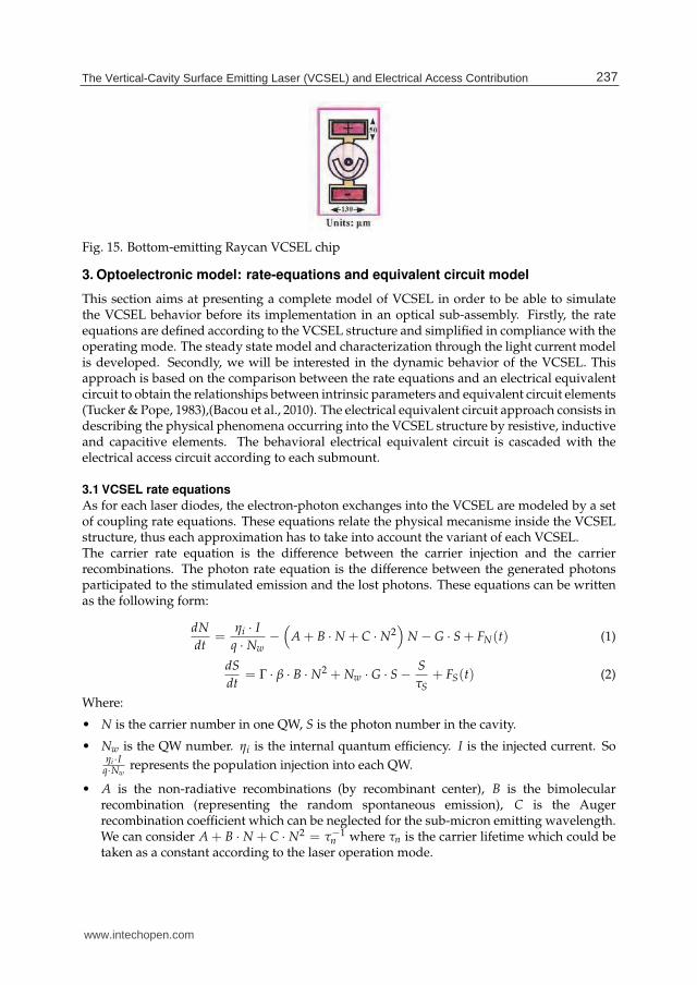
• Bottom-emitting VCSEL chipThe electrical access toplogy previously presented is not adapted to the bottom-emittingVCSEL. The flip-chip bonding is required for the electrical contact. This technique hasthe advantage to be suitable for the integration on a CMOS circuit. Several VCSELmanufacturers provide this kind of chip. Fig.15 shows the topology of a Raycan VCSELchip. In counterpart, the RF testing is difficult because the bottom emission implies theimpossibility of optical power collection.
236 Optoelectronics – Devices and Applications
www.intechopen.com
The Vertical-Cavity Surface Emitting Laser (VCSEL) and Electrical Access Contribution 11
Fig. 15. Bottom-emitting Raycan VCSEL chip
3. Optoelectronic model: rate-equations and equivalent circuit model
This section aims at presenting a complete model of VCSEL in order to be able to simulatethe VCSEL behavior before its implementation in an optical sub-assembly. Firstly, the rateequations are defined according to the VCSEL structure and simplified in compliance with theoperating mode. The steady state model and characterization through the light current modelis developed. Secondly, we will be interested in the dynamic behavior of the VCSEL. Thisapproach is based on the comparison between the rate equations and an electrical equivalentcircuit to obtain the relationships between intrinsic parameters and equivalent circuit elements(Tucker & Pope, 1983),(Bacou et al., 2010). The electrical equivalent circuit approach consists indescribing the physical phenomena occurring into the VCSEL structure by resistive, inductiveand capacitive elements. The behavioral electrical equivalent circuit is cascaded with theelectrical access circuit according to each submount.
3.1 VCSEL rate equations
As for each laser diodes, the electron-photon exchanges into the VCSEL are modeled by a setof coupling rate equations. These equations relate the physical mecanisme inside the VCSELstructure, thus each approximation has to take into account the variant of each VCSEL.The carrier rate equation is the difference between the carrier injection and the carrierrecombinations. The photon rate equation is the difference between the generated photonsparticipated to the stimulated emission and the lost photons. These equations can be writtenas the following form:
dN
dt=
ηi · I
q · Nw−
(
A + B · N + C · N2)
N − G · S + FN(t) (1)
dS
dt= Γ · β · B · N2 + Nw · G · S −
S
τS+ FS(t) (2)
Where:
• N is the carrier number in one QW, S is the photon number in the cavity.
• Nw is the QW number. ηi is the internal quantum efficiency. I is the injected current. Soηi ·I
q·Nwrepresents the population injection into each QW.
• A is the non-radiative recombinations (by recombinant center), B is the bimolecularrecombination (representing the random spontaneous emission), C is the Augerrecombination coefficient which can be neglected for the sub-micron emitting wavelength.We can consider A + B · N + C · N2 = τ−1
n where τn is the carrier lifetime which could betaken as a constant according to the laser operation mode.
237The Vertical-Cavity Surface Emitting Laser (VCSEL) and Electrical Access Contribution
www.intechopen.com

12 Will-be-set-by-IN-TECH
• G is the modal gain. It depends to the carrier and photon number through the relationship
G(N, S) = g0 · N−Ntr1+ǫS where Ntr is the transparency electron number, ǫ is the gain
compression factor. The modal gain coefficient g0 is expressed as g0 = vgr · Γ · aVact
wherea is the differential gain coefficient, Vact is the active layer volume, vgr the group velocityand Γ is the confinement factor.
• The term Γ · β · B · N2 corresponds to the spontaneous emission contributing to the lasingmode. β, the spontaneous emission coefficient, relates the portion of the spontaneousemission which will be amplified.
• τS is the photon lifetime into the cavity. It is linked to the loss by the relationship τ−1S =
vgr · (αi + αm), αi represents the internal losses and αm, the mirror losses.
These equations are adapted to a QW laser through the ηi value and the presence of Nw. Theconfinement factor takes into account the vertical light emission and the DBR contribution.Moreover the values of each intrinsic parameters depend on the VCSEL structure.
The two last term FN(t) and FS(t) have to be taken in part. In fact, FN(t) and FS(t) arethe carrier and photon Langevin functions respectively, representing the carrier and electronfluctuations. These fluctuations are due to the stochastic evolution of N and S associated to thenoise generation. Indeed, the operation of the laser diode is affected by several noise sourceswhose influence varies according to the different regimes. For targeted applications, thepreponderant noise source is the spontaneous emission. The randomness of the spontaneousemission generates amplitude and phase fluctuations of the total optical field. Moreover,these photons which are produced in the laser cavity follow the feedback of the stimulatedphotons and interact with them. By taking into account the wave-corpuscule duality of thelight, a quantum approach is well suited to describe the emission noise generation includingthe photon-electron interaction: each state of photon or electron is associated to a noise pulse.For the purposes of noise generation quantification, recombination and absorption rates in thecavity allow the utilization of the electron and photon Langevin forces to give a mathematicalrepresentation of the optical emission noise.To complete the VCSEL modeling, rate equations have to be solved according to eachoperation mode.
3.1.1 Steady state resolution
The first step of the rate equation resolution considers the case of the steady state. Thisresolution aims at to extract the relationship of the threshold current, threshold carriernumber, and current/photons relations above threshold. It also allows to valid whichapproximation degrees are reliable.When the steady state is reached, the rate equations are equal to 0 such as:
0 =ηi · I
q · Nw−
(
A + B · N + C · N2)
N − G · S (3)
0 = Γ · β · B · N2 + Nw · G · S −S
τS(4)
Fig.16 represents the carrier and photon evolution versus the bias current where the redstraight line corresponds to an asymptotic representation and the dotted line correponds toa physical representation. So we will study both cases begining by an asymptotic resolutioninvolving that the spontaneaous emission Γ · β · B · N2 and the gain compression ǫ · S areneglected.
238 Optoelectronics – Devices and Applications
www.intechopen.com

The Vertical-Cavity Surface Emitting Laser (VCSEL) and Electrical Access Contribution 13
Fig. 16. Evolution of carrier number (N) and photon number S versus the bias current I
• Below threshold: I < Ith, N < Nth et S ≈ 0, according to Fig.16From the equation 3, we can extract:
N =τn · ηi · I
q · Nw, ∀N ≤ Nth (5)
• Above threshold: S > 0 and I > Ith
From the equation 4, we obtain:
Nw · g0 (N − Ntr) =1
τS(6)
Involving:
N = Ntr +1
Nw · τS · g0= cte = NS (7)
Which is equivalent to say : while the simulated emission occures, the carrier number stopsto increase linearly with the current because the carrier consumption is compensated bythe injected current. Thus, we can consider that the carrier number is constant above thethreshold.From the equations 5 and 7, the following relationship could be extracted:
Ith =q · Nw · Nth
ηi · τN(8)
Thus from the equations 3, 6 and 8, we obtain:
S =τS · ηi
q · Nw(I − Ith) (9)
239The Vertical-Cavity Surface Emitting Laser (VCSEL) and Electrical Access Contribution
www.intechopen.com

14 Will-be-set-by-IN-TECH
Then for I > Ith, the photon number linearly increases with the current which verifies thewell-known relationship versus the optical power such as:
Popt = vgr · αm · h · ν · S = ηd ·h · ν
q · Nw(I − Ith) (10)
where ηd is the slope efficiency such as: ηd = ηiαm
αi+αm.
By considering the spontaneaous emission contribution, we can express the real N(I) and S(I)curves close to the threshold according to the dotted line on Fig.16. Henceforth in equation 4,the term Γ · β · B · N is different from zero. As the following equation is valid:
Nw · g0 (Nth − Ntr) =1
τS(11)
The photon rate equation becomes:
0 = Γ · β · B · N2 + g0 · Nw · (N − Nth) · S (12)
So for each injected current, the photon number is not negligible because of the spontaneousemission. Thus, the amplified spontaneous emission is expressed in the followingrelationship:
S =Γ · β · B · N2
g0 · Nw · (N − Nth)(13)
By injecting Equation 13 in Equation 3, the relationship between N and I is written as:
ηi · I
q · Nw−
N
τN− (N − Ntr)
Γ · β · B · N2
Nw · (N − Nth)= 0 (14)
The solution of the 3rd equation corresponds to the evolution of the carrier number close tothe threshold. According to Fig.16 and while I is close to its threshold value, the spontaneaousemission slows the increase of the carrier number to reach the steady-state.
Now, considering the gain compression, that is to say for high value of photon numberinvolving: ǫ · S > 1. The rate equation becomes:
0 =ηi · I
q · Nw−
N
τN− g0
N − Ntr
1 + ǫ · S· S (15)
0 = Nw · g0
[
N − Ntr
1 + ǫ · S− (Nth − Ntr)
]
· S (16)
Thus:
Nth − Ntr
N − Ntr=
1
1 + ǫ · S(17)
and
S =Nw · g0 · τS
ǫ(N − Nth) (18)
By injecting Equations 17 and 18 in Equation 15, we obtain:
ηi · I
q · Nw−
N
τN−
g0
ǫ(N − Nth) = 0 (19)
240 Optoelectronics – Devices and Applications
www.intechopen.com

The Vertical-Cavity Surface Emitting Laser (VCSEL) and Electrical Access Contribution 15
In fact the overflow of the carrier population versus the steady-state value causes an overflowof photon responsible to the gain compression. We can note δN the carrier overflow, so that:N = Nth + ΔN.From the equation 19, we obtain:
δN =ηi
q · Nw
τN · ǫ
τN · g0 + ǫ(I − Ith) = 0 (20)
If τN = 10−9s, ǫ = 10−7, g0 = 104s−1, I − Ith = 10−3 A and ηi = 10−2, δN will beapproximatively equal to 103 which is negligible against Nth. Hence, we can admit the validityof the asymptotic approximation.
3.1.2 Small-signal linearization
Now, the VCSEL is modulated by the superimposition of the bias current I0 and a sinusoidalcurrent ΔI(t) so that ΔI(t) << I0. Due to the small-signal approximation, N(t) and S(t)follow I(t). Let us now linearizing the rate equations according to these conditions. As X(t) =
X0 +ΔX(t) (where X(t) = I(t), N(t) or S(t)), dX0dt = 0 and
dX(t)dt = dΔX(t)
dt . By putting X = dXdt ,
we have dδXdt = δX. As N depends on I, N, S and S on N and S, we have:
ΔN =∂N
∂IΔI +
∂N
∂NΔN +
∂N
∂SΔS (21)
ΔS =∂S
∂NΔN +
∂S
∂SΔS (22)
After linearization, we obtain:
ΔN =ηi
q · NwΔI −
(
g0 ·S0
1 + ǫ · S0+ A + 2 · B · N0 + 3 · N2
0
)
ΔN + g0N0 − Ntr
(1 + ǫ · S0)2
ΔS (23)
ΔS =
(
2 · Γ · β · B · N0 + Nw · g0S0
1 + ǫ · S0
)
ΔN +
(
Nw · g0N0 − Ntr
(1 + ǫ · S0)2−
1
τS
)
ΔS (24)
The equation set can be expressed as follows:
[
ΔNΔS
]
= [M]
[
ΔNΔS
]
+ηi
q · Nw
[
ΔI0
]
(25)
M is a matrix such as:
[M] =
[
−γNN −γNS
γSN −γSS
]
(26)
where:
γNN = A + 2BN0 + 3CN20 +
g0 · S0
1 + ǫ · S0(27)
γNS =g0(N0 − Ntr)
(1 + ǫS0)2(28)
γSN = 2ΓβBN0 +Nw · g0 · S0
1 + ǫS0(29)
241The Vertical-Cavity Surface Emitting Laser (VCSEL) and Electrical Access Contribution
www.intechopen.com

16 Will-be-set-by-IN-TECH
γSS =1
τS−
Nw · g0(N0 − Ntr)
(1 + ǫS0)2(30)
By considering the sinusoidal modulation as ΔI = Im · ejωt, ΔN = Nm · ejωt and ΔS = Sm · ejωt,
and with ddt = jω, the Equation 25 becomes:
[
γNN + jω γNS
−γSN γSS + jω
] [
ΔNΔS
]
=ηi
q
[
ΔI0
]
(31)
By using the Cramer rule, we obtain:
Nm =ηi Im
q
1
Δ
∣
∣
∣
∣
1 γNS
0 γSS + jω
∣
∣
∣
∣
(32)
Sm =ηi Im
q
1
Δ
∣
∣
∣
∣
γNN + jω 1−γSN 0
∣
∣
∣
∣
(33)
where Δ is the matrix determinant such as:
Δ = γNNγSS + γNSγSN − ω2 + jω(γNN + γSS) = ω2R − ω2 + jωγR (34)
ωR is the resonance frequency such as: ω2R = γNNγSS + γNSγSN
et γR is the damping factor: γR = γNN + γPP
Which is conform to a transfer function of a second order system. The resonance frequencyis an important parameters in the determination of the VCSEL frequency bandwidth. Wewill make some approximation according to the small signal regime. By considering a biascurrent I0 above threshold (I > 2 · Ith), in this context, the spontaneous emission and the gaincompression can be neglected. Moreover as we are above threshold, the non-radiative andbimolecular recombination are negligible against the stimulated emission. So γNN , γNS, γSN
and γSS become:γNN = g0 · S0 (35)
γNS = g0(N0 − Ntr) (36)
γSN = Nw · g0 · S0 (37)
γSS =1
τS− Nw · g0(N0 − Ntr) (38)
Which allow us to determine the resonance frequency as:
fR =ωR
2π=
1
2 · π·
√
g0 · S
τS=
√
g0 · ηi
q · Nw(I − Ith) (39)
This relationship is only reliable above threshold. If the bias current had been close to thethreshold, the approximation couldn’t be suitable. Moreover, this resonance frequency doesn’ttake into account the electrical access. We will see how to take into account the electrical accessin a model.
242 Optoelectronics – Devices and Applications
www.intechopen.com

The Vertical-Cavity Surface Emitting Laser (VCSEL) and Electrical Access Contribution 17
Fig. 17. Behavioral equivalent circuit of a 850nm VCSEL
Fig. 18. Small-signal driving of a VCSEL cavity equivelent circuit
3.2 Behavioral equivalent circuit
This approach consists in describing the physical phenomena occuring into the VCSELstructure by an equivalent circuit as shown in Fig.17 for an oxide-confined VCSEL emittingat 850nm. This concept is frequently used in EEL since it has been proposed by R.S Tucker(Tucker & Pope, 1983)in the 80’s. As the electronic funneling through the VCSEL structure isdifferent than the EEL one, the electrical equivalent circuit needs to be adapted by includingthe multi-quantum well (QW), as well as the active layer represented by a RLC resonantcircuit (17): Rj and Cj are associated to the carrier exchanges, L0 and R0 are the photonstorage and resonance damping respectively. For the 850nm VCSEL, the doped DBR, whichis a stack of doped heterojunctions, is equivalent to distributed RC cells: Rmtop and Cmtop
for the top DBR, Rmbottom and Cmbottom for the bottom one. As the current confinement isperformed by an oxide aperture, a RoxCox cell is added to the circuit (Brusenbach et al., 1993).This behavioral electrical equivalent circuit can be directly cascaded with the electrical accessaccording to each submount.By using the linearized rate equation and the Kirchhoff equation of the circuit, relationshipsbetween intrinsic parameters and circuit element can be achieved.As the rate equation considers the carrier number in each QW and the photon number intothe cavity, the Kirchhoff equations are limited to the equivalent circuit of the active region.The equation of the cavity equivalent circuit are expressed according to the convention given
243The Vertical-Cavity Surface Emitting Laser (VCSEL) and Electrical Access Contribution
www.intechopen.com

18 Will-be-set-by-IN-TECH
by Fig.18 where ΔV and ΔI are the input voltage and current respectively, and iL is thephotonic current related to the photon flow variation.
Then, we obtain the following equations:
dΔV
dt=
ΔI
Cj−
ΔV
Rj · Cj−
iL
Cj(40)
diL
dt=
ΔV
L0−
R0 · iL
L0(41)
With these equations the relationship with the instrinsic parameters can be etablished.
3.3 Relationship between rate equation and equivalent circuit
To write the relationships between VCSEL intrinsic parameters and the circuit elements,Equations 23,24,40, 41 have to be compared by using the well-known relationship derivedfrom the voltage-current characteristic of a junction diode:
ΔV
VT=
ΔI
I0=
ΔN
N0(42)
Where VT is assumed to be a constant according to the semiconductor material: VT = m·k·Tq .
Thus:ΔN
dt=
N0
VT·
dΔV
dt(43)
That allow us to obtain directly:
Cj =N0 · q · Nw
VT · ηi(44)
Rj =
[
N0 · q · Nw
VT · ηi·
(
A + 2 · B · N0 + 3 · C · N20 +
g0 · S0
1 + ǫ · S
)]−1
(45)
The relationship between the current iL and the photon fluctuations ΔS is:
g0 ·N0 − Ntr
(1 + ǫ · S0)2=
N0
VT · CjiL (46)
By injecting Equation 46 into Equation 24, we obtain:
L0 =1
Cj·
(1 + ǫ · S)2
go (N0 − Ntr) ·(
2 · Γ · β · B · N0 +g0·S0
1+ǫ·S0
) (47)
R0
L0=
1
τS− g0
N0 − Ntr
(1 + ǫ · S0)2(48)
From the convention of Fig. 18, the resonance frequency can be expressed as follow:
fR =ωR
2 · π=
1
2 · π·
√
1
L0 · Cj+
R0
L0·
1
Rj · Cj(49)
So by modulating the VCSEL in small signal conditions, some intrinsic parameters can beextracted. The task would be easy if the contribution of the electrical access were to be
244 Optoelectronics – Devices and Applications
www.intechopen.com

The Vertical-Cavity Surface Emitting Laser (VCSEL) and Electrical Access Contribution 19
negligeable. In practice, the strong contribution of the electrical access in the frequencyresponse hide the VCSEL response. That’s why the equivalent circuit approach is an excellenttool to cascade the electrical access and the laser diode. We will see how to extract the instrinsicresonance frequency and some intrinsic parameters.
4. VCSEL chip characterisation
As the frequency response of a laser diode is in the microwave domain, the modulationrequired a particular care. Indeed, the driving signal could be consider as a simplecurrent-voltage couple but as an electromagnetic field that propagate as a standing-wave.thus, the connection between the VCSEL and the transmission line being achieved by atransmission line, an impedance matching between the driver and the VCSEL is requiredyet it is not the case of many available VCSEL. This impedance mismatch involves a highreflection on the VCSEL input, that is to say the modulation signal is not totally transmitted tothe VCSEL, and the energy of the electromagnetic field radiates nearby the transmission line.To characterize the VCSEL chip by taking into account the electrical access, the scattering (S)parameters measurement with a vector network analyzer is the most suitable. This methodallows not only to measure the frequency response of the VCSEL but also to extract theelectrical access effect.
4.1 S-parameters measurement
In microwave circuit, the voltage, current and impedance cannot be measured in a directmanner. The measurable quantities are the amplitude and phase of the transmitted waveas compared with those incident wave. These quantities are defined as the Scaterring Matrix(S-Matrix). For a two port system, the S-matrix is written as follow:
[S] =
[
S11 S12
S21 S22
]
(50)
Where:
• S11 is the reflection coefficient on the input (1-port)
• S22 is the reflection coefficient on the output (2-port)
• S21 is the transmission coefficient through the system from the 1-port to the 2-port
• S12 is the transmission through the system from the 2-port to the 1-port
For a laser diode, the S matrix becomes:
[S] =
[
S11 0S21 1
]
(51)
S12 = 0, S22 = 1 if no optical feed-back into laser cavity is considered. So that for themicrowave-photonic S-Matrix measurement, we have to use a device which is able to measurea microwave reflection coefficient (S11) and a microwave-photonic transmission coefficient(S21). To reach this measurement, a Vector Network Analyser (VNA) is required. Theexperimental setup depends on the VCSEL structure (three different emitting wavelengths:850nm, 1310nm and 1550nm) and the electrical access. For the LW-VCSEL, the VNA containsan optical rack able to measure directly the microwave-photonic S21 coefficient. For the 850nmVCSEL, an optical fiber linked to a calibrated photodetector allows the S21 measurementaccording to the experimental setup of Fig.20.
245The Vertical-Cavity Surface Emitting Laser (VCSEL) and Electrical Access Contribution
www.intechopen.com

20 Will-be-set-by-IN-TECH
Fig. 19. RF probe station connected with a vector network analyzer
Fig. 20. Measurement of VCSEL response in opto-microwave domain
Fig. 21. RF probe
For the chip measurement, the VNA is coupled with a probe station as shown by Fig.19.The driving signal is brought by an RF probe as presented in Fig.21.
4.2 Experimental results
The experimental results presented in this section are achieved with the same experimentalsetup presented in the previous section. By thismeasurement technique, the influence of theelectrical access is highlighted for two kind of VCSEL array topology. The TO packagingis excluded for two reasons: it doesn’t allow the driving of only one VCSEL from an array
246 Optoelectronics – Devices and Applications
www.intechopen.com

The Vertical-Cavity Surface Emitting Laser (VCSEL) and Electrical Access Contribution 21
and other extraction techniques have already been presented such as relative intensity noisemeasurement (Majewski & Novak, 1991), subtraction procedure (Cartledge & Srinivasan,1997). So, we will focus on a VCSEL array with microstrip line electrical access and a VCSELarray with coplanar access. The model is validated by comparing the measurement andS-parameters simulation by implementing the equivalent circuit in the ADSTM software (RFsimulation tool).
4.2.1 Microstrip line electrical access
Fig. 22. Crosstalk measurement (blue curve) and simulation (red curve) of a VCSEL arraywith microstip access
Fig. 23. Electrical equivalent circuit of two VCSELs including the crosstalk contribution
The measurement of S-parameters have been achieved on 850nm VCSEL arrays withmicrostrip line access. The microstrip line access requires the submount presented on Fig.13to complete the RF tests and the integration in an optical subassembly. However this circuitinvolves parasitic effects clearly visible on the S11 and S21 measurement and a coupling
247The Vertical-Cavity Surface Emitting Laser (VCSEL) and Electrical Access Contribution
www.intechopen.com

22 Will-be-set-by-IN-TECH
between adjacent VCSEL. As we assume a negligible optical crosstalk, this coupling is theresult of an impedance mismatch due to the wire bonding (Nakagawa et al., 2000). The RFmodulation can circulate on the neighbouring wire by capacitive and inductive coupling.Through these couplings, carriers are injected in the adjacent laser involving a parasitic lightemission. From the S21 measurement, it is thus possible to get the crosstalk versus frequency.Fig.22, printing the crosstalk up to 5GHz, is obtained by the difference between the S21 of thenon-driven VCSEL and the modulated VCSEL.By using the VCSEL electrical equivalent circuit and by the available crosstalk model(represented by a mutual inductance, a parasitic inductance and capacitance), an electricalequivalent circuit of two VCSELs can be developed as shown in Fig.23. The simulation resultsare given by the red curve of Fig.22. The characterization and the modeling of this crosstalkis not significant below 1GHz (less than -35dB) but it increases quickly above this frequency.The degradation of the S21 measurement due to this coupling makes impossible the extractionof reliable value of the VCSEL intrinsic parameters.
4.2.2 Coplanar access
Fig. 24. Comparison between simulated and measured S11 module and phase and S21
module of a 850nm VCSEL
The second kind of measurements is achieved on oxide confined 850nm VCSEL arrays witha coplanar access such as given by Fig.14. The measured scattering parameters of theVCSEL chip including the electrical access are so smouth (without numerical averaging ofthe VNA) that the extraction of the VCSEL cavity S21 becomes available for the extractionof the equivalent circuit elements. According to the range of values of intrinsic parameters
248 Optoelectronics – Devices and Applications
www.intechopen.com

The Vertical-Cavity Surface Emitting Laser (VCSEL) and Electrical Access Contribution 23
and by using the Equations 44,45, 47 and 48, a value of each intrinsic parameters can befixed with a good agreement as it is shown in the comparison between the simulated S21
(Fig.24, red curve) and the measured S21 (Fig.24, blue curve). As the VCSEL tested are
Fig. 25. RC distributed of DBR heterojunctions
Fig. 26. Measured and simulated S11 DBR with 10µm ring contact
850nm oxide confined VCSEL, with a doped DBR, additional measurement can be achievedto extract the DBR equivalent circuit. As aforementioned, DBRs are constituted by a stack ofheterojunctions. Each heterojunction implies RC parallel cell. Consequently, if we consider thewhole DBR, we have as much resistances (Ri) and capacitances (Cj) as interfaces (Brusenbachet al., 1993). By considering that each interface of a DBR is identical, the electrical effects in amirror is represented by an equivalent resistance Rm and capacitance Cm such as:
Cm =Ci
2n − 1(52)
Rm = (2n − 1) · Ri (53)
The top and bottom DBR having different doping and layer pair numbers, the equivalent
Φ Rm Cm Ricalculated Cicalculated Ris imulated Cis imulated
(µm) (Ω) (pF) (Ω) (pF) (Ω) (pF)
10 36 1.43 10.18 5.05 10.21 5.0512 20.8 3 5.88 10.6 5.88 10.614 14.11 2.93 3.99 10.35 3.99 10.35
Table 1. Comparison of the DBR resistances and capacitances
249The Vertical-Cavity Surface Emitting Laser (VCSEL) and Electrical Access Contribution
www.intechopen.com

24 Will-be-set-by-IN-TECH
resistances and capacitances are thus different for the two mirrors.Indeed, DBR stacks have been tested to check the values of the capacitances and resistances.The S11 of 8-p type DBR layer pairs grown by ULM Photonics GmbH (which provided VCSELarrays). The test wafer contains different mesa with a ring contact on the top. Thus, themeasurement is achieved by putting the signal pin of the coplanar probe on the ring contactand the ground pin on the substrate. As the geometry of the wafer hasn’t a coplanar access,the measurement frequency range is limited to 2 GHz (above this frequency the signal isto degraded to be exploited). By using the same approach than the preceeding one, thesmall signal equivalent circuit is implemented in ADSTM software and compared with themeasurements. The characterization having been performed for different mesa diameters, the
Parameters Units Values
A s−1 [1.108; 1, 3.108]B s−1 [0, 7.10−16; 1, 8.10−16] ∗ Vact
Ntr − [0, 83.1024; 4, 4.1024] ∗ Vact
τp ps [1; 6]a m2 [0, 2.10−20; 3, 7.10−20]
Vgr m.s−1 [8, 33.107; 8, 6.107]Γ − [0, 045; 0, 06]β − [10−5; 10−4]ηi − [0, 6; 0, 86]
Table 2. Range of 850 nm VCSEL intrinsic parameters
resistances and capacitances values can be calculated according to Equations 52 and 53 andthe values for each diameters is presented in table 1. Fig.26 gives the comparison betweenthe measurement and the simulation of S11 module of 10µm diameter DBR. The agreementbetween the S11 simulation and measurement is quite good and allows us to implement theRm and Cm values into the VCSEL equivalent circuit.From Equations 44, 45, 47, 48 and the values given by the table 2 for 850nm VCSEL, theintrinsic parameter values are extracted. A, B, β, Ntr, τS, a, vgr, ηi and Γ are obtained byoptimization according to Rj, Cj, L0, R0 and the known VCSEL parameters VT , q, Nw, I0, Ith,Vact. Thus for a 25µm oxide aperture VCSEL, we get the values:VT = 0.063V, Nw = 3, I0 = 2mA, Ith = 0.9mA, τp = 6ps, vgr = 8.5 · 107m/s, a =
1.76 · 10−20m2, β = 104, Γ = 0.049, ηi = 0.6, A = 108 · s−1, B = 88 · s−1, Ntr = 2.41.By the way of the Equation, the extracted values are:
• The threshold carrier number: Nth = 3.04 · 106
• The photon number: S = 2.47 · 104
• The modal gain: G = 5.55 · 1010
• The compression factor:ǫ = 2.11 · 10−6
The model gives then realistic results under certain conditions of VCSEL.For the 1.55µm VCSEL with a coplanar access, the same approache is used. The intracavitycontacts avoid the contribution of the DBR into the electrical circuit. These wavelengths allowto extend the frequency range ut to 20GHz by using the calibrated optical rack with the VNAHP 8510C. However, this frequency increase shows a S21 response with a -60dB/decade slopein spite of the expected -40dB/decade. By knowing that a VCSEL has a -40dB/decade slope,the -60dB/decade slope is assumed to be induced by the electrical access topology (Fig.27).
250 Optoelectronics – Devices and Applications
www.intechopen.com

The Vertical-Cavity Surface Emitting Laser (VCSEL) and Electrical Access Contribution 25
Fig. 27. Measured and extracted S21 responses for a 1.3µm VCSEL at a fixed bias current. Themeasurement takes into account the response of the electrical access as well as the cavitywhile the extracted curve shows the VCSEL cavity response only
Fig. 28. Comparison between simulated and measured S21 module of a 1.55µm VCSEL
This effect has been modeled by using the tranfer matrix (T-matrix) formalism as presentedby A. Bacou in (Bacou et al., 2009) and (Bacou et al., 2010). The method using the T-matrixconsists in the splitting of the VCSEL chip into two cascaded subsystems representing theelectrical access and the optical cavity, respectively. The equivalent electrical circuit definingthe behavior of the electrical access is combined with the T-Matrix formalims to remove theparasitic contribution with the S21 measurement response. The results allow to extract the S21
of the VCSEL as shown by Fig.28 given a -40dB/Decade slope.
5. Conclusion
As it has been presented, the VCSEL technology is in current progress due to its wideadvantages. The vertical emission allows a high integration level offering the possibility of 1Dand 2D array. Due to the small size and the closeness of each VCSEL in an array, the possibilityof electrical coupling on the electrical access is increased particularly for microwave frequencymodulations. That’s why the electrical access has a higher importance than it has for edgeemitting laser diodes. A sight of the consequences of a mismatched electrical access has beenpresented here through a microwave-photonic study based on an electrical equivalent circuitmodel and the S11 and S21 parameters measurements. The results presented for the VCSEL
251The Vertical-Cavity Surface Emitting Laser (VCSEL) and Electrical Access Contribution
www.intechopen.com

26 Will-be-set-by-IN-TECH
array with a microstip-line electrical access shows that influence. Indeed, a coupling betweenthe access lines involves an electrical crosstalk having repercussions on the emitted light bythe VCSEL. The measurements achieved on a VCSEL array with a coplanar access bring theproof that a matched electrical access really improves the frequency response of the VCSELarray. Nevertheless, the matching is reached only for a certain frequency range. For widerfrequency band of measurement, an increase of the S21 slope has been observed. Even if theresponse of the VCSEL has been extracted, the electrical access design has to be improvedfor an impedance matching according to the frequency utilization. Thus this modeling ancharacterisation could further help in the VCSEL design and in the VCSEL integration.
6. References
Baba, T., Yogo, Y., Suzuki, K., Koyama, F. & Iga, K. (1993). Near room temperature continuouswave lasing characteristics of gainasp/inp surface emitting laser, Electronics Letters29(10): 913 –914.
Babic, D., Streubel, K., Mirin, R., Margalit, N., Bowers, J., Hu, E., Mars, D., Yang, L. & Carey, K.(1995). Room-temperature continuous-wave operation of 1.54- mu;m vertical-cavitylasers, Photonics Technology Letters, IEEE 7(11): 1225 –1227.
Bacou, A., Hayat, A., Iakovlev, V., Syrbu, A., Rissons, A., Mollier, J.-C. & Kapon, E. (2010).Electrical modeling of long-wavelength vcsels for intrinsic parameters extraction,Quantum Electronics, IEEE Journal of 46(3): 313 –322.
Bacou, A., Hayat, A., Rissons, A., Iakovlev, V., Syrbu, A., Mollier, J.-C. & Kapon, E. (2009).Vcsel intrinsic response extraction using t -matrix formalism, Photonics TechnologyLetters, IEEE .
Boucart, J., Starck, C., Gaborit, F., Plais, A., Bouche, N., Derouin, E., Goldstein, L., Fortin, C.,Carpentier, D., Salet, P., Brillouet, F. & Jacquet, J. (1999). 1-mW CW-RT monolithicVCSEL at 1.55 µm, IEEE Photonics Technology Letters 11(6): 629–631.
Brusenbach, P., Swirhun, S., Uchida, T., Kim, M. & Parsons, C. (1993). Equivalent circuit forvertical cavity top surface emitting lasers, Electronics Letters 29(23): 2037 –2038.
Cartledge, J. & Srinivasan, R. (1997). Extraction of dfb laser rate equation parameters forsystem simulation purposes, Lightwave Technology, Journal of 15(5): 852 –860.
Esaki, L. (1974). Long journey into tunneling, Proceedings of the IEEE 62(6): 825 – 831.Ibaraki, A., Kawashima, K., Furusawa, K., Ishikawa, T. & Yamaguchi, T. (1989). Buried
heterostructure GaAs/GaAlAs distributed Bragg reflector surface emitting laser withvery low threshold (5.2 mA) under room temperature CW conditions, Japanese Journalof Applied Physics 28: L667+.
Iga, K., Koyama, F. & Kinoshita, S. (1988). Surface emitting semiconductor lasers, QuantumElectronics, IEEE Journal of 24(9): 1845 –1855.
Jewell, J., Scherer, A., McCall, S., Lee, Y., Walker, S., Harbison, J. & Florez, L. (1989).Low-threshold electrically pumped vertical-cavity surface-emitting microlasers,Electronics Letters 25(17): 1123 –1124.
Kapon, E., Sirbu, A., Iakovlev, V., Mereuta, A., Caliman, A. & Suruceanu, G. (2009). Recentdevelopments in long wavelength vcsels based on localized wafer fusion, TransparentOptical Networks, 2009. ICTON ’09. 11th International Conference on.
Kopf, R. F., Schubert, E. F., Downey, S. W. & Emerson, A. B. (1992). N- and p-type dopantprofiles in distributed bragg reflector structures and their effect on resistance, AppliedPhysics Letters 61(15): 1820 –1822.
252 Optoelectronics – Devices and Applications
www.intechopen.com

The Vertical-Cavity Surface Emitting Laser (VCSEL) and Electrical Access Contribution 27
Koyama, F. (2006). Recent advances of vcsel photonics, Journal Of Lightwave TechnologyVol.24(No.12): 4502–4513.
Ly, K., Rissons, A., Quentel, F., Pez, M., Gambardella, E. & Mollier, J.-C. (2008). Bidirectionallink mock-up for avionic applications, IEEE Conference on Avionic FiberOptic (AVFOP),Publisher, San Diego, pp. xx–yy.
Majewski, M. & Novak, D. (1991). Method for characterization of intrinsic and extrinsiccomponents of semiconductor laser diode circuit model, Microwave and Guided WaveLetters, IEEE 1(9): 246 –248.
Nakagawa, S., Hu, S.-Y., Louderback, D. & Coldren, L. (2000). Rf crosstalkin multiple-wavelength vertical-cavity surface-emitting laser arrays, PhotonicsTechnology Letters, IEEE 12(6): 612 –614.
O’Brien, C., Majewski, M. & Rakic, A. (2007). A critical comparison of high-speed vcselcharacterization techniques, Lightwave Technology, Journal of 25(2): 597 –605.
Ortsiefer, M., Shau, R., Böhm, G., Köhler, F., Abstreiter, G. & Amann, M.-C. (2000).Low-resistance inga(al)as tunnel junctions for long wavelength vertical-cavitysurface-emitting lasers, Japanese Journal of Applied Physics 39(Part 1, No.4A): 1727–1729.URL: http://jjap.jsap.jp/link?JJAP/39/1727/
Perchoux, J., Rissons, A. & Mollier, J.-C. (2008). Multimode vcsel model for widefrequency-range rin simulation, Optics Communications 281(1): 162 – 169.
Rhew, K. H., Jeon, S. C., Lee, D. H., Yoo, B.-S. & Yun, I. (2009). Reliability assessment of 1.55-µmvertical cavity surface emitting lasers with tunnel junction using high-temperatureaging tests, Microelectronics Reliability 49(1): 42 – 50.
Rissons, A. & Mollier, J.-C. (2009). Critical study of the vertical-cavity surface emitting laserelectrical access for integrated optical sub-assembly, EMC Europ Workshop, Publisher,Athens, pp. xx–yy.
Rissons, A., Mollier, J., Toffano, Z., Destrez, A. & Pez, M. M. (2003). Thermal andoptoelectronic model of VCSEL arrays for short-range communication, in C. Lei &S. P. Kilcoyne (ed.), Society of Photo-Optical Instrumentation Engineers (SPIE) ConferenceSeries, Vol. 4994 of Society of Photo-Optical Instrumentation Engineers (SPIE) ConferenceSeries, pp. 100–111.
Salet, P., Gaborit, F., Pagnod-Rossiaux, P., Plais, A., Derouin, E., Pasquier, J. & Jacquet, J. (1997).Room-temperature pulsed operation of 1.3 mu;m vertical-cavity lasers includingbottom ingaasp/inp multilayer bragg mirrors, Electronics Letters 33(24): 2048 –2049.
Scott, J., Geels, R., Corzine, S. & Coldren, L. (1993). Modeling temperature effects andspatial hole burning to optimize vertical-cavity surface-emitting laser performance,Quantum Electronics, IEEE Journal of 29(5): 1295 –1308.
Shau, R., Ortsiefer, M., Rosskopf, J., Boehm, G., Lauer, C., Maute, M. & Amann, M.-C.(2004). Long-wavelength inp-based vcsels with buried tunnel junction: propertiesand applications, Vol. 5364, SPIE, pp. 1–15.URL: http://link.aip.org/link/?PSI/5364/1/1
Soda, H., Motegi, Y. & Iga, K. (1983). Gainasp/inp surface emitting injection lasers with shortcavity length, Quantum Electronics, IEEE Journal of 19(6): 1035 – 1041.
Suematsu, Y. & Iga, K. (2008). Semiconductor lasers in photonics, Lightwave Technology, Journalof .
Syrbu, A., Iakovlev, V., Suruceanu, G., Caliman, A., Rudra, A., Mircea, A., Mereuta,A., Tadeoni, S., Berseth, C.-A., Achtenhagen, M., Boucart, J. & Kapon, E. (2004).
253The Vertical-Cavity Surface Emitting Laser (VCSEL) and Electrical Access Contribution
www.intechopen.com

28 Will-be-set-by-IN-TECH
1.55- mu;m optically pumped wafer-fused tunable vcsels with 32-nm tuning range,Photonics Technology Letters, IEEE 16(9): 1991 –1993.
Tucker, R. S. & Pope, D. J. (1983). Microwave circuit models of semiconductor injection lasers,IEEE Transactions On Microwave Theory And Techniques Vol. 31(No. 3): 597–605.
Zhang, J.-P. & Petermann, K. (1994). Beam propagation model for vertical-cavitysurface-emitting lasers: threshold properties, Quantum Electronics, IEEE Journal of30(7): 1529 –1536.
254 Optoelectronics – Devices and Applications
www.intechopen.com

Optoelectronics - Devices and ApplicationsEdited by Prof. P. Predeep
ISBN 978-953-307-576-1Hard cover, 630 pagesPublisher InTechPublished online 03, October, 2011Published in print edition October, 2011
InTech EuropeUniversity Campus STeP Ri Slavka Krautzeka 83/A 51000 Rijeka, Croatia Phone: +385 (51) 770 447 Fax: +385 (51) 686 166www.intechopen.com
InTech ChinaUnit 405, Office Block, Hotel Equatorial Shanghai No.65, Yan An Road (West), Shanghai, 200040, China
Phone: +86-21-62489820 Fax: +86-21-62489821
Optoelectronics - Devices and Applications is the second part of an edited anthology on the multifaced areasof optoelectronics by a selected group of authors including promising novices to experts in the field. Photonicsand optoelectronics are making an impact multiple times as the semiconductor revolution made on the qualityof our life. In telecommunication, entertainment devices, computational techniques, clean energy harvesting,medical instrumentation, materials and device characterization and scores of other areas of R&D the scienceof optics and electronics get coupled by fine technology advances to make incredibly large strides. Thetechnology of light has advanced to a stage where disciplines sans boundaries are finding it indispensable.New design concepts are fast emerging and being tested and applications developed in an unimaginable paceand speed. The wide spectrum of topics related to optoelectronics and photonics presented here is sure tomake this collection of essays extremely useful to students and other stake holders in the field such asresearchers and device designers.
How to referenceIn order to correctly reference this scholarly work, feel free to copy and paste the following:
Angelique Rissons and Jean-Claude Mollier (2011). The Vertical-Cavity Surface Emitting Laser (VCSEL) andElectrical Access Contribution, Optoelectronics - Devices and Applications, Prof. P. Predeep (Ed.), ISBN: 978-953-307-576-1, InTech, Available from: http://www.intechopen.com/books/optoelectronics-devices-and-applications/the-vertical-cavity-surface-emitting-laser-vcsel-and-electrical-access-contribution