HIGH PERFORMANCE ORGANIC TRANSISTORS FOR ORGANIC ...
101
HIGH PERFORMANCE ORGANIC TRANSISTORS FOR ORGANIC ELECTRONIC APPLICATIONS A Dissertation by WON SUK LEE Submitted to the Office of Graduate and Professional Studies of Texas A&M University in partial fulfillment of the requirements for the degree of DOCTOR OF PHILOSOPHY Chair of Committee, Committee Members, Head of Department, Xing Cheng Choongho Yu Jun Zou Weiping Shi Miroslav Begovic May 2017 Major Subject: Electrical Engineering Copyright 2017 Won Suk Lee
Transcript of HIGH PERFORMANCE ORGANIC TRANSISTORS FOR ORGANIC ...

HIGH PERFORMANCE ORGANIC TRANSISTORS FOR ORGANIC ELECTRONIC
APPLICATIONS
A Dissertation
by
WON SUK LEE
Submitted to the Office of Graduate and Professional Studies of
Texas A&M University
in partial fulfillment of the requirements for the degree of
DOCTOR OF PHILOSOPHY
Chair of Committee,
Committee Members,
Head of Department,
Xing Cheng
Choongho Yu
Jun Zou
Weiping Shi
Miroslav Begovic
May 2017
Major Subject: Electrical Engineering
Copyright 2017 Won Suk Lee

ii
ABSTRACT
Thin-film transistor (TFT) devices using organic semiconducting materials have
attracted widespread attentions due to their low cost, flexible form factor, and easy
fabrication. However, organic materials’ poor performance as compared to inorganic
semiconductor such as silicon limits their applications. Specially, high-frequency
operation in organic transistors has never been achieved with organic semiconducting
material. One very attractive application for organic electronics is low-cost and flexible
Radio Frequency Identification Tag (RFID), which requires relatively high frequency
operation. Because of low mobility and high operating bias voltage, the current organic
TFT is not appropriate for the most of applications including RFID.
The objective of this research is to develop the high performance organic
transistor structures which are suitable for organic electronic applications. In designing,
two major performance metrics of devices are focused to be improved, which are the on-
current level with high on-off ratio and the cutoff frequency of the transistors. They are
determined mainly by the carrier mobility, the injection of carrier at the
metal/semiconductor boundary, and the passive parasitic components introduced by
device geometry. In this study, three new structures are investigated, namely dual-
organic layer Metal-Semiconductor Field-Effect Transistor (MESFET), depletion mode
organic Metal-Oxide-Semiconductor Field-Effect Transistor (MOSFET), and organic
Heterojunction Bipolar Transistor (HBT). Each of these devices is optimized to enhance
the performance of the devices based on comprehensive theoretical modeling, and

iii
validated by simulation using TCAD. The devices with channel length of longer than 4
µm exhibit a few µA of on-current and ~10 MHz cutoff frequency. The results obtained
in this work show those novel transistor structures can overcome the weakness of
conventional organic TFTs and have great potential in realizing organic circuit
applications in the future.

iv
ACKNOWLEDGEMENTS
I would like to thank my advisor, Dr. Xing Cheng, for his endless support and
encouragement during my study. Even after his transition to SUSTC, he has kept
providing resources and knowledge to finish my study. I also would like to thank my
committee members, Dr. Choongho Yu, Dr. Jun Zou, and Dr. Weiping Shi for their
guidance and support throughout the course of this research.
Thanks also go to my friends and colleagues and the department faculty and staff
for making my time at Texas A&M University a great experience.
Finally, thanks to my mother and father for their encouragement.

v
CONTRIBUTORS AND FUNDING SOURCES
Contributors
This work was supervised by a dissertation committee consisting of Professor
Xing Cheng [advisor], Professor Jun Zou, and Professor Weiping Shi of the Department
of [Electrical and Computer Engineering] and Professor Choongho Yu of the
Department of [Mechanical Engineering].
The device fabrication for Chapter 3 was collaborated with Bo Yu of the
Department of [Material Science in South University of Science and Technology of
China].
All other work conducted for the dissertation was completed by the student
independently.
Funding Sources
Graduate study was supported by a scholarship, research assistantship, and
teaching assistantship from Texas A&M University.

vi
TABLE OF CONTENTS
Page
ABSTRACT .............................................................................................................. ii
ACKNOWLEDGEMENTS ...................................................................................... iv
CONTRIBUTORS AND FUNDING SOURCES ..................................................... v
TABLE OF CONTENTS .......................................................................................... vi
LIST OF FIGURES ................................................................................................... vii
LIST OF TABLES .................................................................................................... ix
CHAPTER I INTRODUCTION: ORGANIC ELECTRONICS ......................... 1
CHAPTER II BACKGROUND PHYSICS AND MODELING .......................... 4
Carrier Mobility ................................................................................................... 5
Metal/Organic Interfaces ..................................................................................... 11
Organic Defects ................................................................................................... 17
Other Modeling Considerations .......................................................................... 19
Validation of Physics Models by Simulations of OTFT Devices ....................... 22
CHAPTER III DEVICE DESIGN, SIMULATION, AND EXPERIMENT .......... 32
Organic Metal Semiconductor Field Effect Transistor (OMESFET) ................. 32
Depletion Mode Organic Thin Film Transistor (OTFT) ..................................... 49
Organic Heterojunction Bipolar Transistor (OHBT) .......................................... 67
CHAPTER IV SUMMARY AND CONCLUSIONS ............................................. 77
REFERENCES .......................................................................................................... 78
APPENDIX A ........................................................................................................... 84
APPENDIX B ........................................................................................................... 86

vii
LIST OF FIGURES
FIGURE Page
1 Simulated Poole-Frenkel Mobility Model .................................................. 8
2 Simulated Pasveer Mobility Model ............................................................ 10
3 200nm Short Channel OTFT in order to Model Schottky Tunneling ........ 15
4 70nm Short Channel OTFT in order to Model Schottky Tunneling .......... 16
5 Modeled Trap Density of Organic Materials ............................................. 18
6 Illustration of Oxide Charge ....................................................................... 20
7 External Lumped Impedance Modeling ..................................................... 21
8 125μm Long-Channel OTFT Device DC Characteristics .......................... 24
9 50μm Long-Channel OTFT Device DC Characteristics ............................ 25
10 1μm Short-Channel OTFT Device DC Characteristics .............................. 26
11 200nm Short-Channel OTFT Device DC Characteristics .......................... 27
12 70m Short-Channel OTFT Device DC Characteristics .............................. 28
13 AC Response of 125μm and 50μm OTFT ................................................. 29
14 Transient Response of 50μm OTFT ........................................................... 30
15 The Structure and Compact Model of OMESFET ..................................... 36
16 Output Characteristics of Single and Dual Layer OMESFET ................... 39
17 Transfer Characteristics of Single and Dual Layer OMESFET ................. 40
18 AC Response of Single and Dual Layer OMESFET ................................. 41
19 DC Characteristics of OMESFET Experiment Results .............................. 43

viii
20 The Results of Re-fitting Simulations ........................................................ 45
21 DC Characteristics of OMESFET Experiments after Optimization .......... 47
22 The Structure of Depletion Mode OTFT and Compact Model .................. 53
23 Simulation Results of Intrinsic Single-Layer Depletion OTFT ................. 54
24 Simulation Results of Light Doped Single-Layer Depletion OTFT .......... 56
25 Simulation Results of 2% Weight Doped Dual-Layer Depletion OTFT ... 58
26 Simulation Results of 4% Weight Doped Dual-Layer Depletion OTFT ... 60
27 Experiment Results of Intrinsic Single-Layer Depletion OTFT ................ 63
28 Experiment Results of Light Doped Single-Layer Depletion OTFT ......... 64
29 Experiment Results of 2% Weight Doped Dual-Layer Depletion OTFT .. 65
30 Experiment Results of 4% Weight Doped Dual-Layer Depletion OTFT .. 66
31 OHBT Designing Methods and Steps ........................................................ 68
32 Design Structure of OHBT ......................................................................... 68
33 OHBT Energy Band under Operation: Zero and Forward Bias ................. 70
34 Compact Model of OHBT and Reduced Parasitic ..................................... 74
35 Simulation Results of OHBT ..................................................................... 75

ix
LIST OF TABLES
TABLE Page
1 Modeled Pasveer Mobility Parameters ...................................................... 11
2 Modeled Shottky Contact Parameters ........................................................ 16
3 Modeled Parameters of External Elements ................................................ 21
4 Reproduced Simulation Results of Long Channel OTFT .......................... 86
5 Reproduced Simulation Results of Short Channel OTFT .......................... 87
6 Summarized Results and Comparison of OMESFET ................................ 88
7 Summarized Results and Comparison of Depletion OTFT ....................... 89
8 Material Parameters of OHBT ................................................................... 90
9 Summarized Results of OHBT ................................................................... 91
10 Comparison of All Designed High Performance Organic Transistors ....... 92

1
CHAPTER I
INTRODUCTION: ORGANIC ELECTRONICS
Over the years, organic electronic and its potential applications have attracted
widespread attentions in research. Organic transistors can be processed at a low
temperature, and they can be fabricated with easy processing steps, such as printing,
nanoimprinting, and roll to roll [1], [2]. However, organic transistors have many
constraints which limit the use of organic transistor only to a very few applications. As
compared to main stream silicon devices, the most critical disadvantages of organic
transistors are their very poor carrier mobility and their structural feasibility since many
of conventional fabrication methods are unavailable to process organic semiconducting
materials, for instances, ion implantations, and etc. Although there have been so many
efforts to develop novel processing techniques suitable for fabrications of organic
transistors, most of them are focused on MOSFET structure. Some of already developed
and widely used transistors’ structures such as MESFET, depletion mode MOSFET, and
HBT are more feasible to fabricate using organic semiconducting materials without very
sophisticated methods because they can be stacked layer by layer as thin film shapes.
Furthermore, almost infinite number of organic material choice is possible by chemical
synthesizing. Consequently, devices requiring different layers, different doping profiles,
or different energy band parameters can take the advantages from the stacks of thin
organic films. As of these reasons, different structures of organic transistors should be
thoroughly studied and strongly considered as a component of organic electronics.

2
Above mentioned transistor devices, MESFET, depletion mode MOSFET and
HBT are originally designed in need of high performance device for extremely high
speed electronic circuits even in conventional silicon technology. Therefore, the AC
performance of those devices built with organic semiconductors are expected to behave
much better than typical organic MOSFET transistors as well as the DC performance. It
has been reported that the cut off frequency of nanometer range of channel length OTFT
can be up to 10MHz with moderate carrier mobility [3], which is not high considering
the short channel length of nanometer range. As stated earlier, fabricating well behaving
OTFT with such short channel length is very difficult and impossible only with normal
organic processing methods. On the other hand, organic MESFET, depletion mode
OTFT, and Organic Heterojunction Bipolar transistor device are shown that the cut off
frequencies can be up to more than 10MHz even when the channel length is a few micro
meters.
As the first step of the study, short-channel and long channel TFT devices are
simulated by incorporating physical models for materials, interfaces and device
operations. The purpose of this simulation is to validate that the simulation has captured
all essential physical models in device operations. Also, important material and physical
parameters used in these models can be extracted by comparing simulation results with
experimental results published in literature. After that, the OMESFET, depletion mode
OTFT, and OHBT structures are simulated to demonstrate the advantages and weakness
of those organic transistor devices. Finally, the modifications are made for those devices
to optimize the performance of the devices and overcome the weakness of devices. The

3
improvements of performances are demonstrated for both of theoretical simulation
results and experiments results. All the device structures are compatible and built with
normal processing techniques of organic materials.

4
CHAPTER II
BACKGROUND PHYSICS AND MODELING
There are three main different physics explaining organic semiconductors from
inorganic counterparts. Organic semiconductors are not crystalized in atomic level such
as silicon. Instead, they are π-conjugated materials where the charge transport occurs by
hopping from one molecule to other using trap sites of molecules. Therefore, unlike
inorganic semiconductors, the carrier behavior of organic semiconductor is very
different from inorganic semiconductor, which results in that the carrier mobility
depends on the electric field and the carrier concentration, more complicated way than
inorganic semiconductors. This hopping process is not limited only on the behavior of
carrier in the bulk region of semiconductor, but also affects the behavior of carrier at the
interface between electrode and semiconductor. In addition to hopping, another physics
phenomena affects the carrier behavior of injection into semiconductor at the interface of
metal/organic. The permanent electric dipole is formed at the metal/organic interface and
the resulting potential barrier is 0.1eV~0.5eV higher than the expected one aligned by
their workfunction of metal and ionization energy of organic semiconductor. To account
the injection of carrier from electrode accurately, Schottky tunneling and trap assisted
tunneling must be considered as well as thermionic emission over the barrier. In this
chapter, these three physic are investigated thoroughly and modeled by ATLAS TCAD
device simulator.

5
It is worth to note that the material properties of organic semiconductors, such as
carrier mobility, trap density, and the shift of metal workfunction, varies greatly
depending on the choice of material, the degree of chemical contamination, film
morphology, and the process environment. As of this reason, instead of finding the exact
values of material parameters to do fine tuning when modeling the physics, the
generalized parameters were found to reproduce the behavior of device from
experiments.
Carrier Mobility
In organic semiconducting materials, depending on the film, whether it is highly
disordered or highly crystallized, carrier mobility is described by slightly different
mechanisms. Carriers are repeatedly trapped by shallow traps, which are located near
conduction and valence band, and released by thermal agitation. This kind of carrier
transporting behavior is also known as multiple trap and release (MTR) [1], [4].
Another kind of carrier movement in organic semiconductor takes place through deep
level traps located at middle of forbidden band. Since those traps are located in deep
level, trapped carriers are not able to escape only by thermal agitation. Instead, those
carriers jump to the near trap site when applied electric field is high enough [5]. Both of
carrier movements take place in both of highly disordered and highly crystallized
organic materials. In highly crystallized organic semiconductors, the density of deep
level traps is much smaller than highly disordered organic semiconductors. Therefore,

6
crystallized organic semiconductors have much higher carrier mobility and more linear
I-V behavior rather than quadratic I-V behavior.
To model carrier mobility in organic semiconductors accurately, the followings
must be considered: 1) Low-field mobility [6], 2) Carrier concentration dependent
mobility enhancement factor [4], [5], and 3) Field dependent mobility enhancement
factor [7], [8]. The filed independent mobility (low field mobility) can be described as
0
tf
f
effnn
n (1)
Where nf and nt are the number of free carriers and trapped carriers. Equation (1)
explains that the shallow traps close to conduction/valence band slow down the carrier
mobility by continuous trapping and it can be easily modeled by replacing the constant
mobility parameter. Although (1) is an approximated equation and the product of
distributed trap and probability must be integrated to get a complete answer, it is good
enough to model the low field mobility incorporating with shallow traps.
To account for the effect of high electric field, an electric field mobility enhancement
factor must be combined with (1). The field enhancement factor can be written as
F
kT
qexp (2)
Where β is the Poole-Frenkel factor. Combining (1) and (2) gives an equation of electric
field and shallow traps with the fitting parameter γ
F
kT
q
nn
nFT
tf
f exp),( 0 (3)

7
Equation (3) is known as Poole-Frenkel mobility model [7]-[9]. It can be easily noticed
that even very small change of the fitting parameter results in a huge deviation in current
level because of its exponential dependency. Although using the equation reproduce the
tendency of current depending on electric field, it is possible that simulation results are
diverged more than several orders. Also, in our simulation study, ~103 of current level
deviation was observed without adjusting the fitting parameter. Due to this reason,
especially in preceding simulation study before building an actual device, Poole-Frenkel
mobility model is poor at predicting the current-voltage behavior. Figure 1 shows that
how the calculated mobility deviates greatly when the channel length of device is
changed without adjusting the fitting parameters, or when the fitting parameters are
changed while the device size remains same. Because of this reason, equation (3) is
referred as Poole-Frenkel mobility with a limited range of electric field.

8
(a) Short Channel Device
(b) Long Channel Device
Figure 1. Simulated Poole-Frenkel Mobility Model

9
Instead, using unified Gaussian disorder Pasveer model [4] gives us simulation
results excellent matched with experiment results without changing any fitting
parameters and therefore it is much more feasible model to use to design a device and
predict the performance of designed device. In fact, there is no fitting parameter of non-
physics meaning in Pasveer mobility model such as β in Poole-Frenkel mobility model.
The equation of Pasveer mobility model is a fundamentally same form with Poole-
Frenkel mobility and the expression is
),(),(,, 210 FTgnTgFnT (4)
Comparing equation (4) to (3), (4) has another mobility enhancement term g1 included.
The term indicates that carrier mobility also depends on the carrier concentration [4].
The term of g2 is also an exponential function of electric field with better refined range
of electric field. The author of [4] claimed that Pasveer mobility model is better with the
devices which have small Schottky barriers and the range of Gaussian width of densities
less than ~0.2eV. In OTFT devices, the gate voltage reduces the width of Schottky
barrier enough to induce the tunneling at the interface between organic and source/drain
contact, the Pasveer mobility model is also applicable to OTFT devices. Furthermore, in
recent studies of OTFT, as well-ordered materials are used more often rather than highly
disordered ones, it is more reasonable to use the Pasveer mobility model for simulation
study. The calculated carrier mobility is shown in Figure 2 in accordance with the
position. The carrier mobility fits the widely known value of mobility from many
literatures and experiments.

10
(a) Long Channel Device
Short Channel Device
Figure 2. Simulated Pasveer Mobility Model

11
It is also proved that the mobility modeled with Pasveer model agrees with
experiments even when the size of device is changed in the later part of this chapter. The
modeled values of Pasveer mobility are shown in Table 1.
In this study, both of pentacene and P3HT are used to build actual devices since
the energy band parameters of those two materials are almost same. That is, devices are
categorized as polymer devices or small molecule devices for simplicity. Moreover, they
are the most popular organic semiconducting materials used in organic TFT devices.
Table 1. Modeled Pasveer Mobility Parameters
Fitting Parameter Value Variation
α 0.1nm ±0.02
σ 0.1eV +0.05, -0.02
Metal/Organic Interfaces
When an organic material and metal are contacted together without any surface
treatment such as doping or depositing thin layer of surface modifying materials,
Schottly contacts are formed instead of ohmic contact even when using metals with high

12
workfunctions. The shift of metal workfunction is described by several physics
phenomena [10]: 1) charge transfer caused by the difference between a metal
workfunction and the electron affinity and ionization energy of organic film [11], 2)
chemical reaction filling states at the interface and resulting in the shift of Fermi level at
the interface [12], and 3) molecule-induced modification of the metal workfunction,
which is also known as pillow effect [13]. According to [10], the effect of 1) is
negligible compared to 3) since pentacene/P3HT and gold are used in our study. The
category of 2) affects the interface depending on the structure of TFT devices whether it
is top contact or bottom contact, which is the result of fabrication sequence [12]. Our
strategy of modeling the metal/ organic interface for simulation study is that setting the
Schottky barrier height about 0.3~0.5eV as reported in [10] and [12] first, then
performing fine tunings by adjusting Richardson constant and the effective mass of
carrier to control Schottky tunneling and thermionic emission [14] at organic/metal
interface. This method of approximation is not accounted for describing the interface
physics best, but good enough to fit the experiment curves and validating our device
design since this method still includes most of the crucial physics at organic/metal
interface. The Richardson constant which controls both of tunneling and recombination
currents can be described as the equation
3
2* 4
h
mqkA
(5)
Where m is the effective mass of carriers. It is assumed that the effective mass of
majority carrier hole can be varied from 0.5 to 3 from depending on the type of organic

13
thin films, therefore the value is swept in the range to perform a fine tune to fit the
results of experiments.
The one of the most critical performance bottlenecks of organic transistors is
organic/metal interface due to Schottky contact formed, which is not only limiting the
injection of carrier, but also preventing devices from saturating. To minimize the
problem, gold is usually the best choice for P-type transistor most of the time as source
and drain electrodes as the workfunction of gold is 5.1~5.4eV which is close to the
valence band (HOMO level) of organic semiconductor. In case of organic MESFET,
another metal/organic interface exist at gate electrode which is, on the contrary to the
previous case, high Schottky barrier is desirable indeed to prevent the unwanted gate
leakage current [14], [15]. Naturally, aluminum is the most popular choice for gate
electrode to align the workfunction of gate as far as possible from the valence band.
However, the shift of gate metal workfunction toward to valence band makes Schottky
barrier at gate is smaller. Therefore, I-V characteristics at interface must be carefully
modeled and fine tuning of interface parameters must be performed.
The first component of current flowing into the organic from electrode is
described by thermionic emission. This current can be expressed as the equation [14]-
[16]
1expexp,
kT
qV
kTNqJ b
vcs
(6)
Where νs is the surface recombination velocity of carrier and ϕb is the barrier height of
Schottky contact.

14
The other component of current at metal/organic interface is Schottky tunneling
induced by high electric field applied between source and drain metal electrode and
organic semiconductor, or gate metal and organic semiconductor [17]. To model the
Schottky tunneling current in our simulation, the following equation is used.
''1
'1ln'
*
dEEf
EfE
k
TAJ
m
s
E
LT
(7)
Where A* is the Richardson constant, Γ(E) is the tunneling probability, and ƒs(E) and
ƒm(E) are the distribution functions in the semiconductor and metal. In short channel
devices, Schottky tunneling is the dominant current flowing in the device. Thus, without
any modification of interface, the short channel organic transistors do not enter into the
saturation region and the current increases by quadratic function. This is the another
main reason of not fabricating short channel OTFTs besides the increased cost of
building short channel devices.
To model the interface physics, the measured DC characteristics of short channel OTFT
from literature were used because of the two reasons: 1) It is difficult to separate
Schottky tunneling current and thermionic emission current from the total current and 2)
the carrier mobility in organic semiconductor is also strongly depending on the electric
field, in turn, both of Schottky tunneling component and mobility component must be
combined when modeling the behavior of device. It is shown that Schottky tunneling
becomes significant at around 4μm short channel length and starts becoming dominant
over thermionic emission at 1μm from simulations, which depicts that the tunneling
current can be modeled accurately using the DC characteristics of less than 1μm channel

15
length device. In other words, Schottky tunneling current is insignificant in long channel
device such as demonstrated in [18]. Figure 3 and Figure 4 are the simulation results of
200nm and 70nm short OTFT, which are fabricated in [19], with Schottky tunneling
model. The modeled parameters are listed in Table 2.
Figure 3. 200nm Short Channel OTFT in order to Model Schottky Tunneling

16
Figure 4. 70nm Short Channel OTFT in order to Model Schottky Tunneling
Table 2. Modeled Shottky Contact Parameters
Fitting Parameter Value Variation
Richardson Constant (A*) 300 ± 50
Effective Mass (he*) 2.5 ± 0.5

17
Organic Defects
Unlike inorganic single crystalline semiconductors such as silicon, organic
semiconductor materials show that the huge variations of parameters in material
properties depending on morphology, methods of deposition, surface treatment agents,
and etc. That is, the density of traps is not the unique material property and can be varied
under different circumstances. Also, since the behavior of carrier in existence of defects
is modeled with mobility model [4], [5], [9], the main purpose of trap density model is
only to reduce the number of free carriers in organic semiconductor effectively.
Generally, the distribution of trap sites is described with two Gaussian distributions, the
first one is located near the conduction and valence bands, and the other one is located
deeply inside the forbidden band [1], [20]. Then, the number of trapped carriers is
calculated by integrating multiplication of the probability of occupancy and the number
of trap sites over the energy.
dEpn,E,FEgpC
p.trap
E
ED.trapDD.trapped
To maintain the generality with unified Pasveer mobility model, the main
Gaussian peak of trap sites is set to 1020cm-3 and width is set to 0.1eV in order to keep
calculated carrier mobility unaffected by the traps. Instead, only the second Gaussian
peak is adjusted to fit experiment results and perform fine tuning because the deep trap
sites affects the number of trapped carrier mainly and weakly interact with the carrier
mobility [9]. The example of modeled trap density vs. energy is shown in figure 5.

18
Figure 5. Modeled Trap Density of Organic Materials
As shown in figure 5, with 0.1eV of Gaussian width, the second peak of
Gaussian trap density which represents the deep traps of disordered materials is
relatively small number compared to main peak. And therefore, the resulting distribution
of total traps can be approximated as one Gaussian distribution with different Gaussian
width [21].

19
Other Modeling Considerations
The first three parts of this chapter describe the physics inherited in organic
materials. Although those physics models are good enough to model OTFT devices and
reproduce the experiments results with simulations, under the low bias condition, i.e.,
device is turned off or in subthreshold region, the small shift of threshold voltage or
external lumped impedance is better to be included to obtain more accurate simulation
results. The threshold voltage shift is usually occurred by trapped charges between
thermally grown oxide and silicon substrate. For the most case in organic transistors,
bottom gate feature is more commonly used to reduce the number of process steps and it
is easier to fabricate. Therefore, the trapped charge at oxide interface cancels out certain
amount of applied gate voltage or adds off-set voltage to gate. Figure 6 illustrates the
types of trapped oxide charges [22], [23].

20
Figure 6. Illustration of Oxide Charge
Amorphous SiO2, dangling bonds at oxide interface, transition region between
silicon and oxide, and sodium ion contamination while performing thermal growth
introduce four types of oxide charges. Under well controlled industry environment, total
amount of oxide charge is generally,
2
itfotmT QQQQQ cmC1010
However, under lab environment, QT can be increased up to ~1012 C/cm-2.
Another consideration of device modeling is external lumped impedance element
which is caused by the self-impedance of proving point, interfacial impedance, layout
design, and the resistance and inductance of pad which is connected to source and drain
[24]. This is shown in Figure 7.

21
Figure 7. External Lumped Impedance Modeling
The external lumped impedance is measured from comparing the bulk resistance
of organic semiconductor to the resistance of bulk organic semiconductor plus metal
pads. The modeled parameters for oxide charge and external lumped impedance are
listed in Table 3.
Table 3. Modeled Parameters of External Elements
Fitting Parameter Value Variation
QT 1012 C/cm-2 ±20%
RC 10 kΩ -

22
Validation of Physics Models by Simulations of OTFT Devices
In this step, by combining all of the modeled physics above into the device
structure, simulating the device and comparing the simulation results to experiment
results, it is shown that modeling of each physics is valid. To make our further
simulations for new designed devices confident, all the validated material parameters
must be included before proceeding device design based on simulations. In validation
step, experiment results shown in other papers are reproduced by simulation. The
devices we simulate in this step are categorized into long channel, short channel, highly
crystallized small molecule, and disordered polymer. It is assumed that the density of
organic defects and constant mobility can be changed depending on organic film. Other
parameters are kept as same to obtain most accurate simulation results from our own
design.
Figure 8 and Figure 9 are the case of long channel devices and highly crystallized
organic semiconductor in [18]. [18] reports the average carrier mobility of these devices
is ~5 cm2/(Vs) and the highest is up to ~10 cm2/(Vs). As stated previously, the constant
mobility is adjusted to 0.7 cm2/(Vs) to achieve 5 cm2/(Vs) of the saturation mobility with
Pasveer enhancement factor. The simulation results agree with the experiment results
quite accurately.
The second category of verification is the case of short channel devices with
highly disordered organic material. To model this case, the density of traps is increased
and the width of Gaussian density. In addition to the trap density, the constant mobility
parameter is substituted with 0.001 cm2/(Vs). Figure 10, Figure 11, and Figure 12 are the

23
simulation results of short channel and disordered material. As the channel length
becomes shorter near hundreds of nanometers, the simulation results deviate more from
the experiment results reported in [19], although the current level is still in the same
order and the current voltage behavior fits very well. This is possibly due to the poorly
modeled short channel effect in OTFT and the lack of information how they measured
device. For instance, in [19], the author claimed that the gate leakage current is about
2pA with 5nm thickness of gate oxide. This is almost impossible without using high-k
dielectric even in modern silicon devices. Furthermore, in our study, the extremely short
channel devices which are in the range of 100nm are not used.
In addition to the measured DC characteristics, AC simulations are also
conducted for the device which has the experiment result of AC response to obtain
complete device performance results. From the oscillating frequency of ring oscillator in
[18], the cutoff frequency can be extracted by calculation. AC and transient response
simulations are shown in Figure 13 and Figure 14.
The simulation results are summarized in Table 4 and Table 5 and the results
show that these material parameters and modeled physics are valid for our device
simulations.

24
(a) Output Curves
(b) Transfer Curve
Figure 8. 125μm Long-Channel OTFT Device DC Characteristics

25
(a) Output Curves
(b) Transfer Curve
Figure 9. 50μm Long-Channel OTFT Device DC Characteristics

26
(a) Output Curves
(b) Transfer Curves
Figure 10. 1μm Short-Channel OTFT Device DC Characteristics

27
(a) Output Curves
(b) Transfer Curves
Figure 11. 200nm Short-Channel OTFT Device DC Characteristics

28
(a) Output Curves
(b) Transfer Curves
Figure 12. 70nm Short-Channel OTFT Device DC Characteristics

29
(a) Short Circuit Current Gain Vs. Frequency, 125μm Channel Length
(b) Short Circuit Current Gain Vs. Frequency, 50μm Channel Length
Figure 13. AC Response of 125μm and 50μm OTFT

30
DC
VDD=-80V
Vout
Iout
(a) PMOS Inverter to Validate Transient Response
(b) Output Signal of (a) with 10kHz Input Pulse
Figure 14. Transient Response of 50μm OTFT

31
(c) Output Signal of (a) with 100kHz Input Pulse
Figure 14. Continued

32
CHAPTER III
DEVICE DESIGN, SIMULATION, AND EXPERIMENT
In this chapter, based on the issues of performance bottleneck which are stated
previously, three new designed organic transistors are simulated and fabricated. New
designing is involved to: 1) reduce the injection barrier between metal and organic,
hence improve current injection, 2) increase the carrier mobility in the organic region
where the channel is formed, and 3) reduce unwanted parasitic elements. Each transistor
device designed has two or more of enhancing schemes.
Organic Metal Semiconductor Field Effect Transistor(OMESFET)
Unlike MOSFET or TFT structures, the important feature of MESFET structure
is that the gate insulator does not exist. In other words, there must be a potential barrier
to prevent gate leakage current when gate is zero biased or slightly forward biased. It is a
simply Schottky barrier to prevent the unwanted gate leakage current [14], [15].
Consequently, the certain amount of gate leakage current exists even with zero gate bias
due to the behavior of carriers at gate interface. Under any bias condition of normal
MESFET operation, gate is never forward biased and therefore the current induced by
thermionic emission only exist. Since there is a limited choice of metals for gate
electrode, the current flow into the gate by thermionic emission can be controlled weakly.
Although MESFET operates with much smaller voltage range than MOSFET, the carrier
mobility of organic material is very low, the operating voltage can be inevitably up to

33
tens of volts which can contribute tunneling current specially when the size of device
small. Another reason of taking the gate current into the design consideration is that on-
current of MESFET is technically same with off-current of MOSFET. That is, even the
small amount of gate current is possibly significant compared to the on-current of
MESFET. These drawbacks were the motivations to design and suggest the new
MESFET structure.
MESFET is usually on without the gate bias voltage and is turned off when a bias
voltage is applied to the gate. The depletion region under the gate must extend over the
complete thickness of the semiconductor layer to turn off the device. Under zero gate
bias, the semiconductor film thickness must be larger than the depletion region thickness
to form a conduction path between the source and the drain electrodes. Based on the
property of organic material, pentacene is weak P-type without doping, and the
conducting path of the channel in MESFET is electrically neutral. In this case, the
equations of depletion width and the resistance of the conduction channel are derived as
[25], [26]
a
gbis
qN
VVxVxd
])([2
(8)
)]([ xdtWNq
dxdR
a
(9)
Where Na is the acceptor concentration, t is the thickness of the channel, Vbi is the built-
in potential of the Schottky gate contact, and W is the channel width. After substituting
above equations into dV=IdR, the current equation is derived by integrating the
following equation:

34
)]([ xdtWNq
dxIdRIdV
a
dd
(10)
Then, the drain currents are expressed as following for saturation and triode
regions [14], [15]:
21
p
23
gbi
23
gbid
dadV
VVVVV
3
2V
L
WtqμμI (11)
gbi21
p
23
gbip
ad.sat VV3V
VV2
L
V
L
WtqμμI (12)
In equation (11) and (12), Vp is the gate voltage that makes the channel completely
depleted. The voltage is called pinch-off voltage similarly as the case of MOSFET. Note
that the current boundary condition of Schottky barrier is not included in (8)-(12) and
constant mobility is used instead of complete Pasveer mobility. According to (12), the
rough calculation of saturation current is ~0.1 µA with 100 of W to L ratio. The current
will be even lowered when Schottky contact boundary condition is included in the
equation. This low current cancels out the inherent advantages of MESFET device and
eventually the performance of organic MESFET is not much better than organic TFT.
However, our simulation study shows that the performance of organic MESFET is
greatly improved with a little modification of MESFET structure. The idea of improving
organic MESFET is using the doped thin layer as a conducting path of channel below
depletion region formed by gate built-in potential. Figure 15 shows the both structures of
normal MESFET, dual layer MESFET, and derived compact model scheme [27]. In dual
layer MESFET, the acceptor concentration is increased effectively,

35
d
ddAAeffA
txdt
tNxdtNN
))((
))(( .. (13)
Where NA.d is the acceptor concentration of doped layer and td is the thickness of
channel formed in doped layer. If it is assumed that the most part of depletion region
occurs in undoped layer when device is turned on, then the on-current of the device is
also increased to
),(1.
. nTgN
NII
A
dAdDLd (14)
In equation (14), the mobility enhancement factor of carrier concentration
dependency is also included. The adding the doped layer, in turn, inevitably increase the
threshold voltage. The equation (15) is the expression of the threshold voltage for single
layer regular MESFET device, and (16) is derived for suggested dual layer MESFET
device.
s
AbiT
NqtVV
2
2 (15)
s
ddAAdbiT
tNtNqttVV
2
)()( . (16)
By examining the both of equations, it can be known that the threshold voltage
shift can be minimized. To evaluate the complete current continuity equations and obtain
solutions, Silvaco ATLAS TCAD is used for simulation study.

36
Substrate
Undoped LayerSource Drain
Gate
(a) Normal MESFET Structure
Substrate
Undoped LayerSource DrainGate
Doped Layer
(b) Suggested Dual-Layer MESFET Structure
Source DrainGate
(c) Compact Model of MESFET
Figure 15. The Structure and Compact Model of OMESFET

37
The output curves are shown in Figure 16 and the transfer curves are shown in
Figure 17 for both of single layer MESFET and dual-layer MESFET. As shown, dual-
layer MESFET has much higher on-current than single layer MESFET. Of course, the
high current level comes with the price. It trades the high current level off higher Vp,
which means it needs higher voltage to completely deplete the region below gate
electrode since the Fermi level moved down toward valence band in doped thin organic
layer. However, optimized thickness and doping concentration of doped layer can be
minimized the increment of Vp. Fig. 16 clearly indicate that the threshold voltage shifts
only about ~2.8V whereas the saturation current is increased by ~50 times. Even only for
the aspect of DC performance, the dual-layer organic MESFET is superior to the single
layer organic MESFET.
In spite of the fact that superior DC performance of device also indicate the
device can operate at higher frequency, the AC performance of devices are often
determined by inherited and parasitic component including such as overlap capacitance,
depletion capacitance, resistance of depleted region at the end of channel, and etc. In
[18], the ring oscillator was demonstrated and its oscillating frequency was only a few
kHz even with remarkably high DC performance OTFTs. This evidently indicate that the
structure of device is very important even when devices are the same types. In this
section, it is shown that how using dual-layer structure improves the AC performance by
simulations. It can be a possible candidate for low frequency range RFID tags which use
13 MHz frequency signal [20] with fully organic based devices.

38
To calculate the short circuit current gain of the devices, S-parameters is obtained
from simulation first, and the values of S-parameters at each frequency point are
substituted in the equation of
12212211
2
21
1021)1)(1(
2log20
SSSS
SH
(17)
The frequency at which (17) is equal to zero is called the unity gain cutoff frequency
since the magnitude of output current is same with input current. In our simulations, only
common source figure, which is most commonly used, is investigated. The source
electrode of the device is set as the common ground, the gate as the input, and the drain
as the output. The calculated short-circuit current gains are plotted in Figure 18.
Suggested MESFET structure reaches up to 50 MHz of cutoff frequency with
10µm channel length. This dimension size is easily realized under any lab environment,
and with any method of organic processing. It is known that the channel length of OTFT
must be less 200nm and the patterned gate electrode is needed instead of using common
gate for OTFT to reach around ~10MHz cut off frequency [3]. Furthermore, in order to
build the OTFT device with those features, complicated processing methods, such as
shadow masking, are required [3].

39
(a) Single Layer Organic MESFET
(b) Dual Layer Organic MESFET
Figure 16. Output Characteristics of Single and Dual Layer OMESFET

40
(a) Single Layer Organic MESFET
(b) Dual Layer Organic MESFET
Figure 17. Transfer Characteristics of Single and Dual Layer OMESFET

41
(a) Single Layer Organic MESFET
(b) Dual Layer Organic MESFET
Figure 18. AC Response of Single and Dual Layer OMESFET

42
Despite of outperforming characteristics of dual-layer OMESFET, the fabricated
OMESFETs have degraded performance as shown in Figure 19. As gate bias voltage
become larger, the greater gate leakage current flows into gate electrode instead of that
the device is turned off. Since the gate leakage current is steady not quadratic over the
range of drain voltage, it is expected that the leakage current is mainly due to the
thermionic emission rather than Schottky tunneling. In fact, the gate leakage current
could be reproduced by simulations with the increased value of gate workfunction from
4.1eV to 4.6eV and the reduced value of effective hole mass from 3 to 2. Evidently,
aluminum gate metal is damaged during the process of fabrication. The re-fitting
simulation results are shown in Figure 20.

43
0 -10 -20 -30 -40
0.0
-0.5
-1.0
-1.5
-2.0
I D (
A)
VD (V)
VG=0V
VG=10V
VG=20V
VG=30V
VG=40V
VG=50V
(a) Single Layer MESFET: Output Curves
0 10 20 30 40 50
6.3x10⁻⁷
7.9x10⁻⁷
1.0x10⁻⁶
1.3x10⁻⁶
1.6x10⁻⁶
2.0x10⁻⁶
I D (
A)
VG (V)
VD=-40V
(b) Single Layer MESFET: Transfer Curve
Figure 19. DC Characteristics of OMESFET Experiment Results

44
0 -10 -20 -30 -40
0.0000000
-0.0000005
-0.0000010
-0.0000015
-0.0000020
I D (
A)
VD (V)
VG=0V
VG=10V
VG=20V
VG=30V
VG=40V
VG=50V
(c) Dual Layer MESFET: Output Curves
0 10 20 30 40 50
7.9x10⁻⁷
8.9x10⁻⁷
1.0x10⁻⁶
1.1x10⁻⁶
1.3x10⁻⁶
1.4x10⁻⁶
1.6x10⁻⁶
1.8x10⁻⁶
2.0x10⁻⁶
2.2x10⁻⁶
I D (
A)
VG (V)
VD=40V
(d) Dual Layer MESFET: Transfer Curves
Figure 19. Continued

45
(a) Single Layer MESFET: Output Curves
(b) Single Layer MESFET: Transfer Curves
Figure 20. The Results of Re-Fitting Simulations
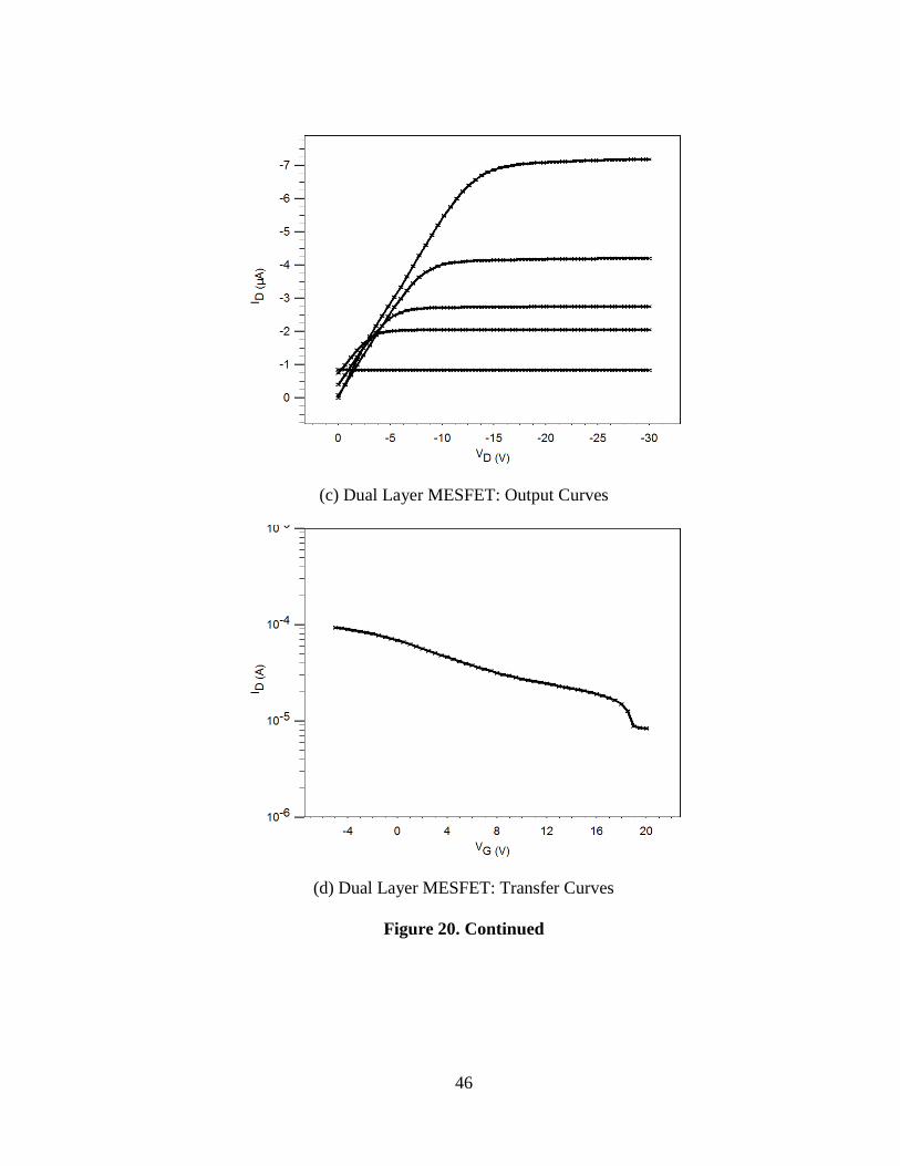
46
(c) Dual Layer MESFET: Output Curves
(d) Dual Layer MESFET: Transfer Curves
Figure 20. Continued

47
By increasing the thickness of aluminum gate, to minimize the effect of
damaging, and after several tries with handling the device very carefully during the
process, OMESFET without gate leakage current could be fabricated. In Figure 21, the
DC characteristics of OMESFET indicate that off-current is still significant and it may
limit the application of device only to analog circuits. The results of OMESFET
simulations and experiments are summarized in Table 6.
0 -10 -20 -30 -40
0.0
-0.5
-1.0
-1.5
-2.0
-2.5
-3.0
-3.5
I D (
A)
VD (V)
VG=0V
VG=10V
VG=20V
VG=30V
VG=40V
(a) Single Layer MESFET: Output Curves
Figure 21. DC Characteristics of OMESFET Experiments after Optimization

48
0 10 20 30 40 50
4.0x10⁻⁸
6.3x10⁻⁸
1.0x10⁻⁷
1.6x10⁻⁷
2.5x10⁻⁷
4.0x10⁻⁷
6.3x10⁻⁷
1.0x10⁻⁶
1.6x10⁻⁶
2.5x10⁻⁶
4.0x10⁻⁶
I D (
A)
VG (V)
VD=-40V
(b) Single Layer MESFET: Transfer Curve
0 -10 -20 -30 -40
0
-10
-20
-30
-40
I D (
A)
VD (V)
VG=0V
VG=10V
VG=20V
VG=30V
(c) Dual Layer MESFET: Output Curves
Figure 21. Continued

49
0 10 20 30 40 50
1.0x10⁻⁷
3.2x10⁻⁷
1.0x10⁻⁶
3.2x10⁻⁶
1.0x10⁻⁵
3.2x10⁻⁵
1.0x10⁻⁴
I D (
A)
VG (V)
VD=40V
(d) Dual Layer MESFET: Transfer Curve
Figure 21. Continued
Depletion Mode Organic Thin Film Transistor(OTFT)
Depletion mode MOSFET is commonly used in silicon technology due to the
high speed of device, less power consumption, and smaller flicker noise performance
[28], [29]. These advantages of silicon device remain intact in organic devices.
Moreover, the issues which cause the poor performance of organic transistors are
resolved by doping the channel region. As stated previously, these issues are 1) high
injection barrier at metal/organic interface, 2) charge trapping by organic defect sites,
and 3) low carrier mobility. Adding P-type dopants in the channel region lower the

50
Fermi level toward valence band, hence the width of Schottky barrier becomes very
narrow and charge injection is facilitated [30]-[33]. Also, the increased number of holes
from dopants fill out the trap sites residing in organic layer and more free carriers exist
without trapping [34], [35]. Consequently, the increased number of free carrier
concentration enhances the carrier mobility by concentration dependent mobility factor,
g2.
As similar as OMESFET, the depletion mode OTFT is usually on without the
gate bias voltage and is turned off when a positive bias voltage is applied to the gate of
p-type transistor. However, unlike OMESFET, the depletion mode OTFT is possible to
be biased with a negative voltage to gate electrode since organic layer is insulated by
dielectric. In this way of gate biasing, even more holes are accumulated in the channel
and higher current level can be reached. This possible bias conditions give more options
to choose in which mode the device operates; complete accumulation mode, depletion
mode, normal depletion mode, and depletion mode with surface inversion. If the device
has a heavily doped and thicker channel below gate metal, then the thickness of
conducting channel is greater than the maximum thickness of depletion layer. In this
case, the transistor never reaches pinch-off condition, and it is hard or impossible to turn
off the device. This type of devices is called Type-B depletion mode MOSFET while
Type-A depletion mode MOSFET has lightly doped channel [28]. One strategy of
increasing the maximum thickness of depletion layer under the channel is depositing
intrinsic organic layer to form a P+-I junction. First, considering single layer of depletion

51
OTFT, the equations of depletion width and the resistance of the conduction channel are
derived similarly as OMESFET,
a
bigi
qN
VV(x)VCxd
][ (18)
)]([ xdtWNq
dxdR
a
(19)
Where Na is the acceptor concentration, t is the thickness of the channel, Vbi is the built-
in potential formed by Fermi level difference between gate electrode and organic layer,
and W is the channel width. For Equation (18), the square root term disappeared from
Equation (8) since the gate insulator exist in depletion mode OTFT. After substituting
above equations into dV=IdR again, the current equation is derived by integrating the
following equation:
)]([ xdtWNq
dxIdRIdV
a
dd
(20)
Then, the drain currents are expressed as following for saturation and triode
regions [26]:
2
ddgT
a
id V2
1VVV
N
n
L
WμCI (21)
2gT
a
id.sat VVN
n
L
WμC
2
1I (22)
In equation (21) and (22), VT is pinch-off or threshold voltage which makes the
thickness of depletion region same as the thickness of conducting channel. For the
simplicity of deriving equation, Schottky contact boundary condition of source and drain

52
contacts are excluded. Adding the enough dopants in the channel region make the
number of free carriers n almost same with Na. However, if the doping concentration is
too high then, the pinch-off voltage Vp becomes large and device starts to behave as
resistor rather than transistor. Assuming that the doping concentration is high enough
only to fill out the traps of organic film, but not high enough to make the transistor as
resistor, then Equation (21) and (22) become,
2
ddgTi1d V2
1VVV
L
WCnT,μgI (23)
2gTi1d.sat VVL
WCnT,μg
2
1I (24)
It indicates that the higher current level can be achieved by both of the mobility
enhancement factors of carrier concentration dependency and reduced trap sites.
Nevertheless, another DC performance of device is degraded because the pinch-off
voltage increases, so that the device becomes difficult to be turned off even with very
large gate voltage resulting in low on-off current ratio. Equation (25) gives the
explanation of this.
bi
i
AT V
C
NqtV
(25)
To minimize the increment of pinch-off voltage, only thin layer right underneath
the channel is doped while the second organic layer remains intrinsic as shown in Figure
22.
Now, the effective doping concentration becomes

53
Gate
SiO2 DrainSource
Doped Layer
Figure 22. The Structure of Depletion Mode OTFT and Compact Model
d
ddAAeffA
txdt
tNxdtNN
))((
))(( .. (26)
Where NA.d is the acceptor concentration of doped layer and td is the thickness of
channel formed in doped layer. Equation (26) is substitute in Equation (25) and the new
equation of pinch-off voltage is
bi2A1d
i
T Vt
tNtN
C
qtV
(27)
By optimizing the both of thickness and doping concentration, it can be known
that the threshold voltage shift can be minimized.
The output curves, transfer curve, and AC response are shown in Figure 23-26
with different doping concentration for both of single layer depletion mode OTFT and
dual layer depletion mode OTFT. As shown, dual-layer depletion mode OTFT has much
higher on-current than single layer one, reaching 0.4mA.

54
(a) Single Layer Depletion OTFT: Output Curves
(b) Single Layer Depletion OTFT: Transfer Curves
Figure 23. Simulation Results of Intrinsic Single-Layer Depletion OTFT

55
(c) Single Layer Depletion OTFT: Short Circuit Current Gain Vs. Frequency
Figure 23. Continued

56
(a) Single Layer Depletion OTFT: Output Curves
(b) Single Layer Depletion OTFT: Transfer Curves
Figure 24. Simulation Results of Light Doped Single-Layer Depletion OTFT

57
(c) Single Layer Depletion OTFT: Short Circuit Current Gain Vs. Frequency
Figure 24. Continued

58
(a) Dual Layer Depletion OTFT: Output Curves
(b) Dual Layer Depletion OTFT: Transfer Curves
Figure 25. Simulation Results of 2% Weight Doped Dual-Layer Depletion OTFT

59
(c) Dual Layer Depletion OTFT: Short Circuit Current Gain Vs. Frequency
Figure 25. Continued

60
(a) Dual Layer Depletion OTFT: Output Curves
(b) Dual Layer Depletion OTFT: Transfer Curves
Figure 26. Simulation Results of 4% Weight Doped Dual-Layer Depletion OTFT

61
(c) Dual Layer Depletion OTFT: Short Circuit Current Gain Vs. Frequency
Figure 26. Continued
As shown in the Figure 26, the device cannot be pinched off with the doping
concentration of 5×1017cm-3 and above, and therefore the off current of device is high.
AC performance is remarkable even with such a long channel length of 10μm. The
depletion mode OTFT can reach 10MHz of cutoff frequency. Under the assumption of
that the cutoff frequency increases approximately linear by scaling the channel length,
then the cutoff frequency of 1μm of smaller channel length device is expected to have
the unity gain frequency located at around 100MHz.
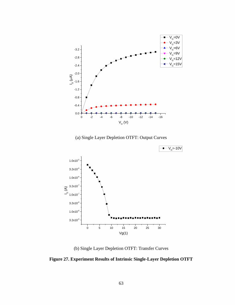
To verify the design and simulation, actual devices are fabricated and measured,
and measured results are shown in Figure 27~30 in accordance with different doping

62
concentration and structure. It clearly indicates that depletion mode OTFT has very high
on-current level, lower operation voltage, high cutoff frequency, and it can be applicable
to many organic electronic applications. One down side or possible limitation is the high
off current. There are several ways of solving this problem which is verified by
simulations and modeling. First, adding another contact at the intrinsic layer similar as
body contact of silicon MOSFET or dual gate scheme. In this way, the ability to control
the conductivity of channel is improved and makes easier to turned off the device.
Second method is using the N-doped layer instead of intrinsic layer. However, N-type
organic material is much more unstable and much more careful passivation of device is
necessary to protect N-type material. Also, both methods are required to process extra
additional steps, so those device structures are not fabricated at this time.
The results of depletion mode OTFT simulations and experiments are
summarized in Table 7.
63
0 -2 -4 -6 -8 -10 -12 -14 -16
0.0
-0.4
-0.8
-1.2
-1.6
-2.0
-2.4
-2.8
-3.2
I D (
A)
VD (V)
VG=0V
VG=3V
VG=6V
VG=9V
VG=12V
VG=15V
(a) Single Layer Depletion OTFT: Output Curves
0 5 10 15 20 25 30
3.2x10⁻⁹
1.0x10⁻⁸
3.2x10⁻⁸
1.0x10⁻⁷
3.2x10⁻⁷
1.0x10⁻⁶
3.2x10⁻⁶
1.0x10⁻⁵
I D (
A)
Vg(1)
VD=-10V
(b) Single Layer Depletion OTFT: Transfer Curves
Figure 27. Experiment Results of Intrinsic Single-Layer Depletion OTFT

64
0 -10 -20 -30 -40
0.0
-0.4
-0.8
-1.2
-1.6
-2.0
-2.4
-2.8
-3.2
-3.6
-4.0
I D (
A)
VD (V)
VG=0V
VG=5V
VG=10V
VG=15V
VG=20V
(a) Single Layer Depletion OTFT: Output Curves
-20 -10 0 10 20 30
3.2x10⁻⁸
1.0x10⁻⁷
3.2x10⁻⁷
1.0x10⁻⁶
3.2x10⁻⁶
1.0x10⁻⁵
I D (
A)
Vg(3)
VD=-40V
(b) Single Layer Depletion OTFT: Transfer Curves
Figure 28. Experiment Results of Light Doped Single-Layer Depletion OTFT

65
0 -10 -20 -30 -40
0
-3
-6
-9
-12
-15
I D (
A)
VD (V)
VG=0V
VG=5V
VG=10V
VG=15V
VG=20V
(a) Dual Layer Depletion OTFT: Output Curves
-20 -10 0 10 20 30
1.0x10⁻⁷
3.2x10⁻⁷
1.0x10⁻⁶
3.2x10⁻⁶
1.0x10⁻⁵
3.2x10⁻⁵
1.0x10⁻⁴
3.2x10⁻⁴
I D (
A)
VG (V)
VD=-40V
(b) Dual Layer Depletion OTFT: Transfer Curves
Figure 29. Experiment Results of 2% Weight Doped Dual-Layer Depletion OTFT

66
0 -2 -4 -6 -8 -10 -12 -14 -16
0
-3
-6
-9
-12
-15
-18
-21
-24
I D (
A)
VD (V)
VG=0V
VG=5V
VG=10V
VG=15V
VG=20V
(a) Dual Layer Depletion OTFT: Output Curves
-10 0 10 20 30
3.2x10⁻⁷
1.0x10⁻⁶
3.2x10⁻⁶
1.0x10⁻⁵
3.2x10⁻⁵
1.0x10⁻⁴
I D (
A)
VG (V)
VD=-20V
(b) Dual Layer Depletion OTFT: Transfer Curves
Figure 30. Experiment Results of 4% Weight Doped Dual-Layer Depletion OTFT

67
Organic Heterojunction Bipolar Transistor(OHBT)
The last device studied in this research is organic heterojunction bipolar
transistor, which can actually resolve all the issues involving with organic transistor
devices by very high doping concentration, minimized parasitic components and current
mode mechanism rather than field effect via capacitor. The challenging parts of OHBT
are organic material selection and physical etching of organic layers without causing
damages. Since two different materials with different energy band, possibly three
different materials in case that N-type doping is unavailable, it is better to synthesize the
material chemically rather than using commercially available organic materials. Because
of this reason, the attempt to fabricate OHBT device has not been made in this research.
The fabrication part will remain as a future work and OHBT is only designed by TCAD
after thorough investigation and study theoretically. All the material parameters are
designed according to the widely known organic band parameters [36]-[37] , so that
OHBT device is feasible to be fabricated. By following the designing steps illustrated in
Figure 31, all the designed material parameters are listed in Table 8. Also, the designed
structure is shown in Figure 32.

68
Figure 31. OHBT Designing Methods and Steps
Figure 32. Design Structure of OHBT

69
The parameters of materials listed above are determined to ensure the operation
of typical inorganic HBT device. The base/emitter heterojunction makes the potential
barrier seen by base electrons in the conduction band is higher than that seen by emitter
holes in the valence band. Thus, for a given base/emitter bias, the ratio of holes injected
to electrons injected will be higher, and thus the gain will be higher [38], [39]. The band
gap difference enables to keep a thin and highly doped base at the same time, which
results in a very high cutoff frequency and high gain [40]. One different feature from
inorganic HBT is that the doping concentration of sub-collect is very high. In inorganic
HBT, light doped sub collector is preferred since it is desirable for all of the collected
carrier to flow into the collector electrode without scattering. That is, light doped sub-
collector gives carriers higher mobility. In contrast to inorganic HBT, to increase the
carrier mobility in sub-collector region, high doping concentration is preferable. In fact,
since the operation voltage of HBT is extremely small compared to field effect organic
transistor and thus applied electric field is not high enough to increase the mobility, the
only way to increase the carrier mobility is to keep carrier concentration as high as
possible in organic HBT. The designed OHBT device is shown in Figure 33, and it
illustrates the mechanism of operation.

70
(a) Spatial Hole Concentration in the Device under Zero Bias
(b) Energy Band Diagram of Emitter-Base-Collector under Zero Bias
Figure 33. OHBT Energy Band under Operation: Zero and Forward Bias

71
(c) Hole Concentration of Emitter-Base-Collector under Zero Bias
(d) Spatial Hole Concentration in the Device under Forward Bias
Figure 33. Continued

72
(e) Energy Band Diagram of Emitter-Base-Collector under Forward Bias
(f) Hole Concentration of Emitter-Base-Collector under Forward Bias
Figure 33. Continued

73
Figure 33 indicate that the hole injection barrier is 0.1eV while the electron
injection barrier is 0.3eV between emitter and base junction. The thickness of emitter
layer is optimized to prevent injected electrons from base reaching to the emitter
electrode, and the thickness of base is kept thin enough to ensure injected holes from
emitter to reach the end of base at the same time in according to the designing step
shown in Figure 31. Another important feature revealed in Figure 33 is that the width of
injection barrier at the interface between emitter contact and organic emitter layer is less
than 10nm which is narrow enough to be considered as ohmic contact rather than
Schottky contact. Therefore, higher transconductance gain and lower contact resistance
are achieved in this design. To evaluate complete device performance, the compact
model of OHBT is first derived as shown in Figure 34 [41], [42].
From the complete compact model of OHBT with structure in Figure 34, it can
be easily understood that the parasitic elements are reduced by heavy doping. According
to the equation of depletion region width (28) and the equation of cutoff frequency (29),
the cutoff frequency can be calculated.
VVqN
2εX bi
sdep (28)

74
C
Csc
n
2
BB
jcCEc
jcje
m
e
ec
t
2υ
Xτ
2D
Xτ
CRRτ
CCg
1τ
2ππ
1f
(29)
Finally, the simulation results of OHBT are shown in Figure 35 and summarized
in Table 9.
Emitter
Base
Collector
Figure 34. Compact Model of OHBT and Reduced Parasitic

75
(a) DC Characteristic: Forward Gummel
(b) DC Characteristic: IC Vs.VC Output Curves
Figure 35. Simulation Results of OHBT

76
(c) AC Characteristic: Short Circuit Current Gain Vs. Frequency
Figure 35. Continued

77
CHAPTER IV
SUMMARY AND CONCLUSION
In this research, three different organic transistor structures are investigated with
simulations and experiments. Modified organic MESFET and depletion mode OTFT
devices by using the dual-layer scheme can improve the performance of devices for both
of DC (higher on-current) and AC (higher operating frequency) performance as shown
in simulations and experiments results. OHBT is likely have superior performance to all
the currently existing organic transistor structures based on simulations. The dual-layer
organic MESFET device can operate with a nominal voltage of less than 10 V and
operate at a frequency up to 50 MHz, and the depletion mode OTFT device can operate
with a nominal voltage of 20 V and operate at a frequency up to 10 MHz. The
performance of the devices will be further improved when highly crystallized organic
materials. With 10MHz or higher cutoff frequencies, those devices can be possible
candidates to build low frequency range RFID tags, LCD backplane panel and many
other large area electronic circuits with full organic integration. All the performances of
devices are summarized in Table 10.
As for the future works, each of essential components of electronic circuit will be
built with organic materials, and complete integrated circuit system will be demonstrated.

78
REFERENCES
[1] G. Horowitz, “Organic Field-Effect Transistors,” Adv. Mater., vol. 10, no. 5, pp.
365-377, Mar. 1998.
[2] C. D. Dimitrakopoulos and P. R. L. Malenfant, “Organic Thin Film Transistors
for Large Area Electronics,” Adv. Mater., vol. 14, no. 2, pp. 99-117, Jan. 2002.
[3] F. Ante, D. Kalblein, U. Zschieschang, T. W. Canzler, A. Werner, K, Takimiya,
M. Ikeda, T. Sekitani, T. Someya, and H. Klauk, “Contact Doping and Ultrathin
Gate Dielectrics for Nanoscale Organic Thin-Film Transistors,” Small., vol. 7, no.
9, pp. 1186-1191, May. 2011.
[4] S. L. M. can Mensfoort and R. Coehoorn, “Effect of Gaussian Disorder on the
Voltage Dependence of the Current Density in Sandwich-Type Devices Based on
Organic Semiconductors,” Phys. Rev. B., vol. 78, no. 8, pp. 085207-1-085207-16,
Aug. 2008.
[5] M. C. J. M. Vissenberg and M. Matters, “Theory of the Field-Effect Mobility in
Amorphous Organic Transistors,” Phys. Rev. B., vol. 57, no. 20, pp. 12964-
12967, May. 1998.
[6] V. I. Arkhipov, P. Heremans, E.V. Emelianova, G.J. Adriaenssens, and H.
Bassler, “Charge Carrier Mobility in Doped Semiconducting Polymers,” App.
Phys. Lett., vol. 82, no. 19, pp. 3245-3247, Jun. 2003.
[7] H. Bassler, “Charge Transport in Disordered Organic Photoconductors a Monte
Carlo Simulation Study,” Phys. Stat. Sol., vol. 175, no. 1, pp. 15-56, Jan. 1993.

79
[8] Y. N. Gartstein and E. M. Conwell, “High-Field Hopping Mobility in Molecular
Systems with Spatially Correlated Energetic Disorder,” Chem. Phys. Lett., vol.
245, no. 4-5, pp. 351–358, Nov 1995.
[9] M. Bouhassoune, S. L. M. can Mensfoort, P. A. Bobbert, and R. Coehoorn,
“Carrier-Density and Field-Dependent Charge-Carrier Mobility in Organic
Semiconductors with Correlated Gaussian Disorder,” Org. Electron., vol. 10, no.
3, pp. 437-445, May. 2009.
[10] A. Kahn, N. Koch, and W. Gao, “Electronic Structure and Electrical Properties
of Interfaces between Metals and π-Conjugated Molecular Films,” J. Poly. Sci.
B., vol. 41, no. 21, pp. 2529–2548, Nov. 2003.
[11] I. G. Hill, J. Schwartz, and A. Kahn, “Metal-Dependent Charge Transfer and
Chemical Interaction at Interfaces between 3,4,9,10-Perylenetetracarboxylic
Bisimidazole and Gold, Silver and Magnesium,” Org. Electron., vol. 1, no. 1, pp.
5–13, Dec. 2000.
[12] N. J. Watkins, L. Yan, and Y. Gao, “Electronic Structure Symmetry of Interfaces
between Pentacene and Metals,” App. Phys. Lett., vol. 80, no. 23, pp. 4384–4386,
Apr. 2002.
[13] H. Vazquez, Y. J. Dappe, J. Ortega, and F. Flores, “Energy Level Alignment at
Metal/Organic Semiconductor Interfaces: “Pillow” Effect, Induced Density of
Interface States, and Charge Neutrality Level,” J. Chem. Phys, vol. 126, no. 14,
pp. 144703-1-144703-8, Apr. 2007.

80
[14] S. M. Sze and K. N. Kwok, Physics of Semiconductor Devices, 3rd ed. Hoboken,
NJ: Wiley, 2006.
[15] B. L. Anderson and R. L. Anderson, Fundamentals of Semiconductor Devices,
1st ed. Avenue of the Americas, NY: McGrawHill, 2005.
[16] J. C. Scott and G. G. Malliaras, “Charge Injection and Recombination at the
Metal-Organic Interface,” Chem. Phys. Lett., vol. 299, no. 2, pp. 115–119, Jan.
1999.
[17] K. Matsuzawa, K. Uchida, and A. Nishiyama, “A Unified Simulation of Schottky
and Ohmic Contacts,” IEEE Trans. Electron Devices, vol. 47, no. 1, pp. 103-108,
Jan. 2000.
[18] J. Li, Y. Zhao, H. S. Tan, Y, Guo, C. Di, G. Yu, Y. Liu, M. Lin S. H. Lim, Y.
Zhou, H. Su, and B. S. Ong, “A Stable Solution-Processed Polymer
Semiconductor with Record High-Mobility for Printed Transistors,” Sci. Rep.,
vol. 2, no. 754, Oct. 2012.
[19] M. D. Austin, and S. Y. Chou, “Fabrication of 70 nm channel length polymer
Organic Thin-Film Transistors Using Nanoimprint Lithography,” Appl. Phys.
Lett., vol. 81, no. 23, pp. 4431-4433, Dec. 2002.
[20] Z. Bao and J. Locklin, Organic Field-Effect Transistors, 1st ed. Boca Raton, FL:
CRC Press, 2007.
[21] M. Hack, J. G. Shaw, P. G. LeComber, and M. Willums, “Numerical Simulation
of Amorphous and Polycrystalline Silicon Thin-Film Transistor,” Jpn. J. Appl.
Phys., vol. 29, no. 12, pp. L2360-L2362, Dec. 1990.
81
[22] Y. C. Yeo, T. J. King, and C. Hu, “Metal-Dielectric Band Alignment and Its
Implications for Metal Gate Complementary Metal-Oxide-Semiconductor
Technology,” J. Appl. Phys., vol. 92, no. 12, pp. 7266-7271, Dec. 2002.
[23] C. C. Hu, Modern Semiconductor Devices for Integrated Circuits, 1st ed. Upper
Saddle River, NJ: Pearson, 2010.
[24] C. S. Rafferty, M. R. Pinto, and R. W. Dutton, “Iterative Methods in
Semiconductor Device Simulation,” IEEE Trans. Electron Devices, vol. CAD-4,
no. 4, pp. 462-471, Oct. 1985.
[25] A. Takshi and A. Dimopoulos, “Simulation of a Low-Volatge Organic Transistor
Compatible with Printing Methods,” IEEE Trans. Electron Devices, vol. 55, no. 1,
pp. 276-282, Jan. 2008.
[26] G. Horowitz, R. Hajlaoui, and F. Kouki, “An Analytical Model for the Organic
Field-Effect Transistor in the Depletion Mode. Application to Sexithiophene
Films and Single Crystals,” Eur. Phys. J. AP, vol. 1, no. 3, pp. 361-367, Mar.
1998.
[27] B. L. Ooi and J. Y. Ma, “Consistent and Reliable MESFET Parasitic Capacitance
Extraction Method,” IEE Proc. Microw. Antennas Propag., vol. 151, no. 1, pp.
81-84, Feb. 2004.
[28] U. Kumar, “Analysis and Modeling of Depletion-Mode MOS Transistors,”
Active and Passive Elec. Comp., vol. 19, no. 2, pp. 73-89, Jul. 1995.

82
[29] D. A. Divekar and R. I. Dowell, “A Depletion-Mode MOSFET Model for Circuit
Simulation,” IEEE Trans. Comput.-Aided Des. Integr. Circuits Syst., vol. CAD-3,
no. 1, pp. 80-87, Jan. 1984.
[30] X. Liu, D. Kasemann and K. Leo, “Top-Gate Organic Depletion and Inversion
Transistors with Doped Channel and Injection Contact,” Appl. Phys. Lett., vol.
106, no. 10, pp. 103301-1-103301-4, Feb. 2015.
[31] B. L. Max, L. Tietze, H. Kleemann, C. HoBbach, J. W. Bartha, A. Zakhidov and
K. Leo, “Doped Organic Transistors Operating in the Inversion and Depletion
Regime,” Nat. Commun., vol. 4, no. 2775, pp. 1-6, Oct. 2013.
[32] P. Pacher, A. Lex, V. Proschek, H. Etschmaier, E. Tchernychova, M. Sezen, U.
Scherf, W. Grogger, G. Trimmel, C. Slugovc, and E. Zojer, “Chemical Control of
Local Doping in Organic Thin-Film Transistors: From Depletion to
Enhancement,” Adv. Mater., vol. 20, no. 16, pp. 3143-3148, Jul. 2008.
[33] P. Cosseddu, J. Vogel, B. Fraboni, J. P. Rabe, N. Koch, and A. Bonfiglio,
“Continuous Tuning of Organic Transistor Operation from Enhancement to
Depletion Mode,” Adv. Mater., vol. 21, no. 3, pp. 344-348, Nov. 2008.
[34] P. Stallinga and H. L. Gomes, “Modeling Electrical Characteristics of Thin-Film
Field-Effect Transistors I. Trap-Free Materials,” Synthetic. Metals., vol. 156, no.
21-24, pp. 1305-1315, Nov. 2006.
[35] P. Stallinga and H. L. Gomes, “Modeling Electrical Characteristics of Thin-Film
Field-Effect Transistors II. Effects of Traps and Impurities,” Synthetic. Metals.,
vol. 156, no. 21-24, pp. 1316-1326, Nov. 2006.

83
[36] M. Estrada, I. Mejia, A. Cerdeira, J. Pallares, L. F. Marsal and B. Iniguez,
“Mobility Model for Compact Device Modeling of OTFTs Made with Different
Materials,” Solid-State Electron., vol. 52, no. 5, pp. 787-794, May. 2008.
[37] O. Marinov, M. J. Deen and B. Iniguez, “Charge Transport in Organic and
Polymer Thin-Film Transistors: Recent Issues,” IEE Proc.-Circuits Devices Syst.,
vol. 152, no. 3, pp. 189-207, June. 2005.
[38] J. Mcmacken, S. Nedeljkovic, J. Gering and D. Halchin, “HBT Modeling,” IEEE
Microwave Magazine, vol. 9, no. 2, pp. 276-282, Apr. 2008.
[39] W. Liu, Handbook of III-V Heterojunction Bipolar Transistors, New York, NY:
Wiley-Interscience, 1998.
[40] C. T. Kirk, “A Theory of Transistor Cutoff Frequency (fT) Falloff at High
Current Densities,” IRE Trans. Electron Devices., vol. 9, no. 2, pp. 164-174, Mar.
1962.
[41] M. W. Dvorak and C. R. Bolognesi, “On the Accuracy of Direct Extraction of the
Heterojunction-Bipolar-Transistor Equivalent-Circuit Model Parameters Cπ, CBC,
and RE,” IEEE Trans. Microwave Theory Tech., vol. 51, no. 6, pp. 1640-1649,
June. 2003.
[42] B. Li and S. Prasad “Basic Expressions and Approximations in Small-Signal
Parameter Extraction for HBT’s,” IEEE Trans. Microwave Theory Tech., vol. 47,
no. 5, pp. 534-539, May. 1999.

84
APPENDIX A
DEVICE FABRICATION
For MESFETs, 30nm of gold was deposited on Corning EXG200 glass substrate
using thermal evaporation. Then, Source/drain electrodes were patterned by
photolithography and wet etching. Aluminum gate electrodes were patterned by liftoff
process. AZ5214 was used in its image reversal mode. After lithography, the substrate
was etched in the gate area to a depth of 37nm utilizing the resist as the etch mask. 40nm
of aluminum was deposited by thermal evaporation then. The resist was striped in
solvent thereafter and finally the gate was patterned. The liftoff process enables burying
the gate electrode in the substrate. Therefore, it allows us to accurately mimic the layout
design in the simulation. After all the electrodes were successfully fabricated, both
polymeric and small-molecule organic semiconductors were deposited by spin coating
and thermal evaporation respectively.
Doping concentration, types of materials and semiconductor layer thickness were
varied for the optimization of device performance.
For depletion mode OTFTs, heavily doped n type silicon was used as the
substrate with its body as the common gate. 300nm thermal dioxide was used as the
insulator dielectric for the long channel devices. For short channel devices, aluminum
oxide was used instead of silicon dioxide for its high permittivity and film density to
suppress the gate leakage current and short channel effects. Source/Drain electrodes
were patterned with liftoff process. Electron beam lithography was conducted with

85
ZEP520 resist and then 3nm Cr & 30nm gold was evaporated. After resist stripping,
P3HT and pentacene were deposited as the active layer. Different doping concentration
and film thickness were applied to find out the optimize device performance.

86
APPENDIX B
LARGE TABLES
Table 4. Reproduced Simulation Results of Long Channel OTFT
Long Channel Experiment* Modeled by Simulation
L=125μm L=50μm L=125μm L=50μm
Threshold Voltage ~6V ~6V ~8V ~6V
Operating Voltage -60V -40V -60V -40V
On-Current 250μA 240μA 240μA 240μA
On-Off Ratio ~108 ~108 ~1010 ~1010
Cutoff Frequency(Device)
~1.2kHz×5×20 25kHz 80kHz
Saturation Mobility 2.5 3 1.75 2

87
Table 5. Reproduced Simulation Results of Short Channel OTFT
Short Channel Experiment* Modeled by Simulation
L=1μm L=200nm L=70nm L=1μm L=200nm L=70nm
Threshold Voltage 2V 3V 4V 2V 3V 4V
Operating Voltage -3V -3V -3V -3V -3V -3V
On-Current 2.8nA 5.5nA 26nA 2.4nA 7nA 11nA
On-Off Ratio ~104 ~104 ~104 ~1010 ~1010 ~105
Cutoff Frequency(Device) - - - - - -
Saturation Mobility 0.01 0.01 0.01 0.01 0.01 0.01

88
Table 6. Summarized Results and Comparison of OMESFET
Experiment Modeled by Simulation
Single Layer Dual Layer Single Layer Dual Layer
Threshold Voltage ~40V ~40V ~3.5V ~3.5V
Operating Voltage -40V -40V -4V -4V
On-Current 3μA 35μA 0.8μA 38μA
On-Off Ratio ~60 ~320 ~103 ~103
Cutoff Frequency(Device)
700kHz 20MHz
Saturation Mobility 0.075 0.1~0.3 0.02 0.2

89
Table 7. Summarized Results and Comparison of Depletion OTFT
Experiment Modeled by Simulation
Single Layer Dual Layer Single Layer Dual Layer
Threshold Voltage ~18V ~15V ~2V ~12V
Operating Voltage -20V -15V -5V -15V
On-Current 4μA 22μA 8μA 380μA
On-Off Ratio ~300 ~100 ~1012 ~103
Cutoff Frequency(Device)
100kHz 10MHz
Saturation Mobility 0.013 0.3 0.038 0.5
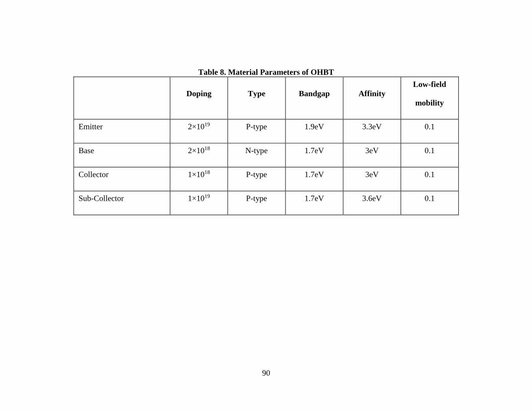
90
Table 8. Material Parameters of OHBT
Doping Type Bandgap Affinity
Low-field
mobility
Emitter 2×10¹⁹ P-type 1.9eV 3.3eV 0.1
Base 2×10¹⁸ N-type 1.7eV 3eV 0.1
Collector 1×10¹⁸ P-type 1.7eV 3eV 0.1
Sub-Collector 1×10¹⁹ P-type 1.7eV 3.6eV 0.1

91
Table 9. Summarized Results of OHBT
Experiment Modeled by Simulation
Threshold Voltage To be measured ~0.9V
Operating Voltage
-2V
On-Current
1mA
On-Off Ratio
~1012
Cutoff Frequency(Device)
1GHz
Saturation Mobility
1.8

92
Table 10. Comparison of All Designed High Performance Organic Transistors
Dual Layer OMESFET Dual Layer Dep OTFT OHBT
Experiment Simulation Experiment Simulation Simulation
Threshold Voltage ~40V ~3.5V ~15V ~12V ~0.9V
Operating Voltage
-40V -4V -15V -15V -2V
On-Current 35μA 38μA 22μA 380μA 1mA
On-Off Ratio ~320 ~103 ~100 ~103 ~1012
Cutoff
Frequency(Device)
20MHz
10MHz 1GHz
Saturation Mobility
0.1~0.3 0.2 0.3 0.5 1.8