Flexible organic transistors and circuits with extreme … · SUPPLEMENTARY INFORMATION doi:...
12
SUPPLEMENTARY INFORMATION DOI: 10.1038/NMAT2896 NATURE MATERIALS | www.nature.com/naturematerials 1 SUPPLEMENTARY INFORMATION Flexible organic transistors and circuits with extreme bending stability Tsuyoshi Sekitani, Ute Zschieschang, Hagen Klauk & Takao Someya 1. Device Fabrication and characterization Organic thin-film transistors (TFTs) and integrated circuits were fabricated on 12.5 m thick, highly flexible polyimide film (see Figure 1a). The schematic cross-section of the TFTs is shown in Figure 1b. In the first step of the fabrication process, the substrate was coated with a 500 nm thick polyimide planarization layer, which was deposited by spin-coating and cured for 5 hours at a temperature of 180 ºC in nitrogen. The planarization layer reduces the surface roughness of the flexible substrate from 2.5 nm to 0.32 nm RMS, which is essentially identical to the surface roughness of a polished single-crystalline silicon wafer (see Figures S1 and S2). The gate electrodes of the transistors were prepared on the surface of the planarization layer by evaporating a nominally 20 nm thick layer of aluminum (Al) through a shadow mask. A 4 nm thick layer of aluminum oxide (AlO x ) was then created on the Al surface by an oxygen plasma treatment (10 min at a plasma power of 100 W). The substrate was then immersed in a 2-propanol solution of n-octadecylphosphonic acid to create a densely packed organic self-assembled monolayer (SAM) with a thickness of 2 nm on the oxidized Al surface. The total thickness of the gate dielectric is therefore 6 nm, and it has a capacitance per unit area of 0.6~0.65 F/cm 2 . 50 nm thick layers of the organic semiconductors pentacene (for the p-channel TFTs) and F 16 CuPc (for the n-channel TFTs) were then deposited by vacuum sublimation through shadow masks. The source and drain contacts were prepared on top of the organic semiconductors by evaporating gold (Au) to a thickness of 50 nm through a shadow mask. Finally, a polymer/metal encapsulation stack (300 nm thick parylene, 200 nm thick gold, and 12.5 μm thick parylene) was deposited in order to protect the transistors from air-induced degradation. Consequently, all measurements reported below were carried out in ambient air. Furthermore, the deposition of the 13 m thick encapsulation stack places the TFTs and circuits at the neutral strain position. All measurements were performed in air. TFT characteristics were measured using an Agilent 4155C parameter analyzer with a sweep rate of about 0.1 V/sec. Figures 2b and 2c show the output and transfer characteristics of a pentacene p-channel TFT, and Figures 2d and e show the characteristics of a F 16 CuPc n-channel TFT. The hysteresis seen in Figures 2c and 2e is very small, indicating that the bias-stress effect and the density of active impurities are negligible. 2. Substrate Bending To evaluate the bending stability of the TFTs, the substrate was bent along an axis running exactly through the transistors. To determine whether the angle between the direction of the bending-induced mechanical strain and the direction of the drain current in the TFTs has any effect, we fabricated TFTs in which the drain current flows parallel to the strain direction as well as TFTs in which the drain current flows perpendicularly to the strain direction (see Figure 3). The strain S induced in a particular layer having a thickness t L located on the surface of a substrate having a thickness t S by bending the substrate into a radius R is given by the following equation: ( )( ) + + + + + = 1 1 2 1 R 2 t t S 2 S L (1) where = t L /t S , = Y L /Y S , Y L is Young’s modulus of the layer and Y S is Young’s modulus of the substrate [S1]. Figure S6 shows how the drain currents and gate currents of pentacene TFTs on a 75 m thick polyimide substrate change upon bending. From Figure S6 it can be seen that the smallest radius into which the substrate can be bent before the TFTs degrade is 3.5 mm. According to Equation (1) this corresponds to a strain S = 1%, assuming t L = 106 nm (the total thickness of the TFTs), t S = 75 m (the polyimide substrate thickness), and Y L Y S . This suggests that 1% is the maximum compressive strain that pentacene TFTs can withstand. By reducing the substrate thickness from 75 m to 13 m, the bending radius at which the strain reaches 1% is reduced from 3.5 mm to 600 m. However, Figure 3 shows that pentacene TFTs fabricated on a 13 m thick polyimide substrate can be bent into a radius of 100 m before degradation sets in. This is because the TFTs in Figure 3 were encapsulated with a 13 m thick parylene/Au/parylene stack, so that the TFTs are located at the neutral strain position and the compressive strain from the substrate and the tensile strain from the encapsulation layer cancel each other at the position of the TFTs. Because of the excellent adhesion of the parylene encapsulation layer, this structure is robust during bending to a radius as small as about 100 μm, indicating an excellent robustness of contact between source/drain electrodes and organic semiconductors. However, © 2010 Macmillan Publishers Limited. All rights reserved.
Transcript of Flexible organic transistors and circuits with extreme … · SUPPLEMENTARY INFORMATION doi:...
SUPPLEMENTARY INFORMATIONdoi: 10.1038/nmat2896
nature materials | www.nature.com/naturematerials 1
1
SUPPLEMENTARY INFORMATION
Flexible organic transistors and circuits with extreme bending stability
Tsuyoshi Sekitani, Ute Zschieschang, Hagen Klauk & Takao Someya
1. Device Fabrication and characterization
Organic thin-film transistors (TFTs) and integrated circuits
were fabricated on 12.5 m thick, highly flexible polyimide
film (see Figure 1a). The schematic cross-section of the TFTs
is shown in Figure 1b.
In the first step of the fabrication process, the substrate was
coated with a 500 nm thick polyimide planarization layer,
which was deposited by spin-coating and cured for 5 hours at a
temperature of 180 ºC in nitrogen. The planarization layer
reduces the surface roughness of the flexible substrate from
2.5 nm to 0.32 nm RMS, which is essentially identical to the
surface roughness of a polished single-crystalline silicon wafer
(see Figures S1 and S2).
The gate electrodes of the transistors were prepared on the
surface of the planarization layer by evaporating a nominally
20 nm thick layer of aluminum (Al) through a shadow mask. A
4 nm thick layer of aluminum oxide (AlOx) was then created
on the Al surface by an oxygen plasma treatment (10 min at a
plasma power of 100 W). The substrate was then immersed in
a 2-propanol solution of n-octadecylphosphonic acid to create
a densely packed organic self-assembled monolayer (SAM)
with a thickness of 2 nm on the oxidized Al surface. The total
thickness of the gate dielectric is therefore 6 nm, and it has a
capacitance per unit area of 0.6~0.65 F/cm2.
50 nm thick layers of the organic semiconductors pentacene
(for the p-channel TFTs) and F16CuPc (for the n-channel
TFTs) were then deposited by vacuum sublimation through
shadow masks. The source and drain contacts were prepared
on top of the organic semiconductors by evaporating gold (Au)
to a thickness of 50 nm through a shadow mask.
Finally, a polymer/metal encapsulation stack (300 nm thick parylene, 200 nm thick gold, and 12.5 μm thick parylene) was
deposited in order to protect the transistors from air-induced
degradation. Consequently, all measurements reported below
were carried out in ambient air. Furthermore, the deposition of
the 13 m thick encapsulation stack places the TFTs and
circuits at the neutral strain position.
All measurements were performed in air. TFT characteristics
were measured using an Agilent 4155C parameter analyzer
with a sweep rate of about 0.1 V/sec. Figures 2b and 2c show
the output and transfer characteristics of a pentacene p-channel
TFT, and Figures 2d and e show the characteristics of a
F16CuPc n-channel TFT. The hysteresis seen in Figures 2c and
2e is very small, indicating that the bias-stress effect and the
density of active impurities are negligible.
2. Substrate Bending
To evaluate the bending stability of the TFTs, the substrate
was bent along an axis running exactly through the transistors.
To determine whether the angle between the direction of the
bending-induced mechanical strain and the direction of the
drain current in the TFTs has any effect, we fabricated TFTs in
which the drain current flows parallel to the strain direction as
well as TFTs in which the drain current flows perpendicularly
to the strain direction (see Figure 3).
The strain S induced in a particular layer having a thickness tL
located on the surface of a substrate having a thickness tS by
bending the substrate into a radius R is given by the following
equation:
( )( )++
+++=
11
21
R2
ttS
2
SL (1)
where = tL/tS, = YL/YS, YL is Young’s modulus of the layer
and YS is Young’s modulus of the substrate [S1].
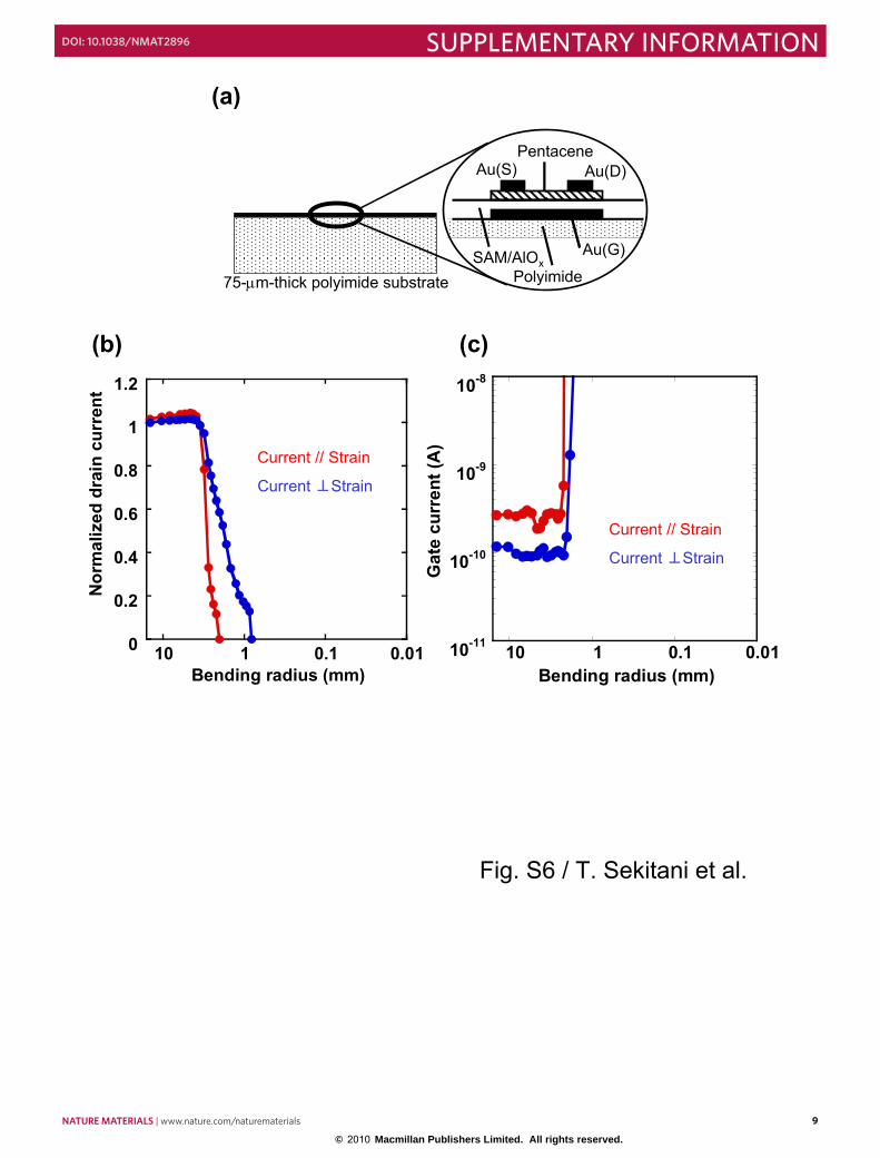
Figure S6 shows how the drain currents and gate currents of
pentacene TFTs on a 75 m thick polyimide substrate change
upon bending. From Figure S6 it can be seen that the smallest
radius into which the substrate can be bent before the TFTs
degrade is 3.5 mm. According to Equation (1) this corresponds
to a strain S = 1%, assuming tL = 106 nm (the total thickness of
the TFTs), tS = 75 m (the polyimide substrate thickness), and
YL YS. This suggests that 1% is the maximum compressive
strain that pentacene TFTs can withstand.
By reducing the substrate thickness from 75 m to 13 m, the
bending radius at which the strain reaches 1% is reduced from
3.5 mm to 600 m. However, Figure 3 shows that pentacene
TFTs fabricated on a 13 m thick polyimide substrate can be
bent into a radius of 100 m before degradation sets in. This is
because the TFTs in Figure 3 were encapsulated with a 13 m
thick parylene/Au/parylene stack, so that the TFTs are located
at the neutral strain position and the compressive strain from
the substrate and the tensile strain from the encapsulation layer
cancel each other at the position of the TFTs. Because of the
excellent adhesion of the parylene encapsulation layer, this
structure is robust during bending to a radius as small as about 100 μm, indicating an excellent robustness of contact between
source/drain electrodes and organic semiconductors. However,
© 2010 Macmillan Publishers Limited. All rights reserved.
2 nature materials | www.nature.com/naturematerials
SUPPLEMENTARY INFORMATION doi: 10.1038/nmat2896
SUPPLEMENTARY INFORMATION
2
further decrease in bending radii results in damages in the gate
dielectric of the transistors (See Figure 3c).
3. Operation speed
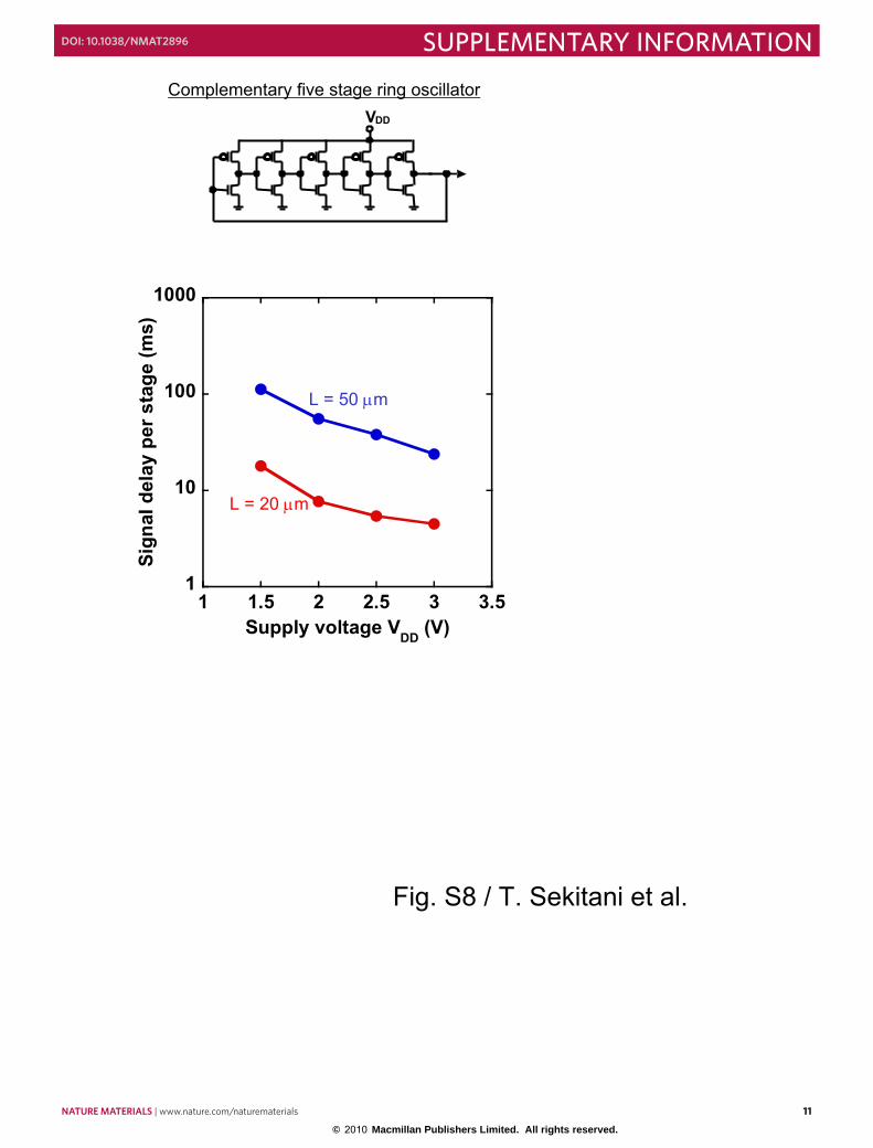
As summarized in Figure S8, signal delay of the ring oscillator
depends, not only on channel length (L), but also on supply
voltage, VDD. The smallest signal delay on our complementary
five stage ring oscillator is 4.5 ms, whose signal delays in the
range of a few milliseconds are good enough for certain sensor
applications like artificial skins, as highlighted in Figures 1
and 5. For example, the real-time scanning (the frame rate of 2
Hz) for a 100-by-100 sensory array can be achieved by the
transistors with frequency response of about 5 ms with line-
scanning method. In such sensor applications, mechanical
durability and operation voltage are often more important than
high operation speed.
When we compare our results with silicon-based circuits [S2],
our organic circuits are slower than silicon ones, however, the
silicon circuits were bent with a radius of only 4.5 mm. In
contrast, our organic ring oscillator continues to operate
without any change in electrical performance while being
folded into a radius of 300 m.
We would like to compare our results with previous organic
transistor-based circuits. It is very important to compare the
results among different structures at the same voltage, since
the signal delay depends on the supply voltage: In general,
circuits operated with larger voltage have smaller signal delay.
Note that the unipolar circuits [S3] were operated with a
supply voltage of 50 V, while our complementary circuits
operate with much more battery-friendly voltages between 1.5
and 3 V. It is true that the signal delay of our flexible organic
complementary ring oscillator (4.5 ms) is larger than that of
some previously reported unipolar organic circuits [S3], due to
the relatively small mobility of n-channel organic
semiconductors. Compared with unipolar circuits, however,
complementary circuits have much lower power consumption
and are thus much more attractive for practical applications.
Nevertheless, the flexible ring oscillator we show in this work
is as fast as organic complementary circuits made on rigid
glass [S4].
References
[S1] Gleskova, H., Wagner, S., Soboyejo, W., & Suo, Z.
Electrical response of amorphous silicon thin-film
transistors under mechanical strain. J. Appl. Phys. 92,
6224-6229 (2002).
[S2] Kim, D. H., Ahn, J. H., Kim, H. S., Lee, K. J., Kim, T. H.,
Yu, C. J., Nuzzo, R. G., & Rogers, Complementary
Logic Gates and Ring Oscillators on Plastic Substrates by
Use of Printed Ribbons of Single-Crystalline Silicon. J.
A., IEEE Electron Device Lett., 29, 73-76 (2008)
[S3] Klauk, H., Halik, M., Zschieschang, U., Eder, F., Schmid,
G., & Dehm, C. Pentacene organic transistors and ring
oscillators on glass and on flexible polymeric substrates.
Appl. Phys. Lett., 82, 4175-4177 (2003).
[S4] Klauk, H., Zschieschang, U., Pflaum, J. & Halik, M.
Ultralow-power organic complementary circuits. Nature
445, 745-748 (2007).
© 2010 Macmillan Publishers Limited. All rights reserved.
nature materials | www.nature.com/naturematerials 3
SUPPLEMENTARY INFORMATIONdoi: 10.1038/nmat2896
SUPPLEMENTARY INFORMATION
3
Figure caption of the Supplementary Information
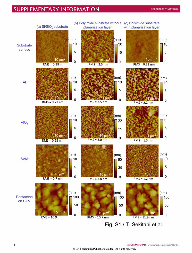
Figure S1. Surface roughness of the individual layers of organic TFTs fabricated on three different substrates. Using atomic force microscopy (AFM) we have measured
the root-mean-square (RMS) surface roughness of the individual layers of which an organic thin-film transistor (TFT) is composed. Organic TFTs were fabricated on three different substrates: a, A thermally oxidized, single-crystalline silicon (Si/SiO2) wafer. b, A 12.5 m thick polyimide substrate without planarization layer. c, A 12.5 m thick polyimide substrate with a 500 nm thick polyimide planarization layer. AFM images were taken (from top to bottom): of the substrate, after the deposition of the Al gate
electrodes, after the oxygen-plasma-induced oxidation of the Al gates, after the formation of the phosphonic-acid self-assembled monolayer (SAM), and after the deposition of the pentacene semiconductor layer on the AlOx/SAM gate dielectric.
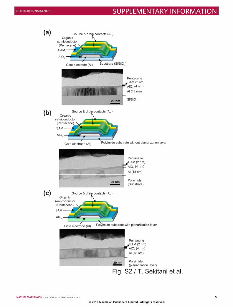
Figure S2. Schematic cross-sections and high-resolution transmission electron microscope (TEM)
images of organic TFTs fabricated on three different substrates. a, Pentacene TFT fabricated on a thermally oxidized, single-crystalline silicon (Si/SiO2) wafer. b, Pentacene TFT fabricated on a 12.5 m thick polyimide substrate without planarization layer. c, Pentacene TFT fabricated on a 12.5 m thick polyimide substrate with a 500 nm thick polyimide planarization layer. The surface of the planarized polyimide substrate (and thus the individual
TFT layers on this substrate) are almost atomically smooth, similar to the situation on the Si/SiO2 substrate.
.
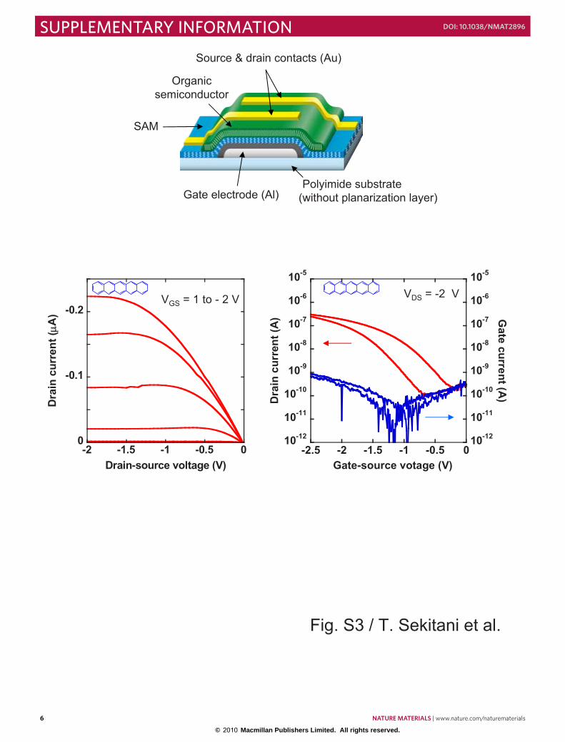
Figure S3. Current-voltage characteristics of a pentacene TFT fabricated on a polyimide substrate without planarization layer. When the planarization layer is omitted, the surface on which the TFTs are fabricated is much rougher, so the morphology of the pentacene films
does not facilitate a high degree of orbital overlap between the conjugated molecules, resulting in poor TFT performance, including low field-effect mobility (0.01 cm
2/Vs),
large hysteresis, and small on/off ratio.
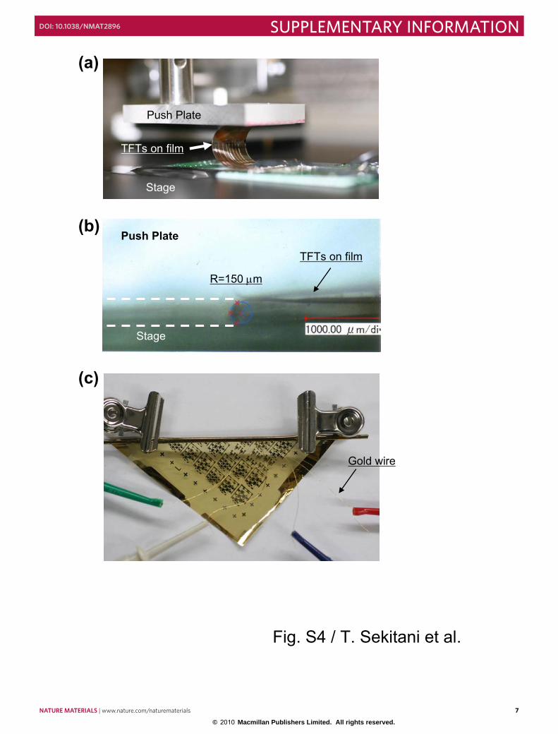
Figure S4. Photographs taken during bending tests. a, Photograph of the custom-built bending apparatus in action. b, The exact bending radius was determined from digital photographs taken along the bending axis. c, Photograph of
a substrate with organic TFTs and circuits wrapped around a cylinder with a radius of 300 m. Fine gold wires are used to connect the TFTs and circuits to a semiconductor parameter analyzer to facilitate electrical testing in the bent state.
Figure S5. Capacitance of Al/AlOx/SAM/Au capacitors fabricated on 12.5 m thick polyimide substrates with a 500 nm thick polyimide planarization layer as a function
of bending radius. The blue curve shows the capacitance measured on a capacitor with a 13 m thick parylene encapsulation stack (so this capacitor is located in the neutral strain position). The red curve shows the capacitance of a capacitor without encapsulation (so this capacitor is not located in the neutral strain position). For both curves the capacitance (C) is normalized to the capacitance measured in the flat state (C0 = 0.65 F/cm
2).
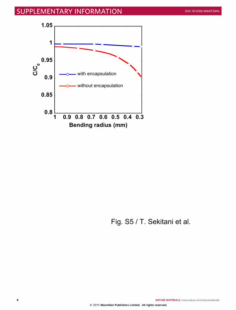
Figure S6. Bending stability of pentacene TFTs fabricated on thicker substrates (thickness 75 m instead of 12.5 m) without encapsulation stack. In this case, the TFTs are not located in the neutral strain position of the substrate and thus are stable only to a bending radius of about 3.5 mm (as opposed to 100 m, as was shown in Figure 3). Drain-source voltage: -2 V, gate-source voltage: -2.5 V.
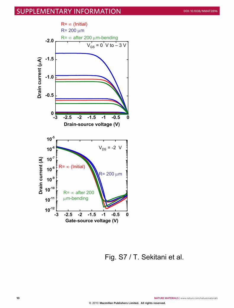
Figure S7. Electrical characteristics of a pentacene TFT before, during and after bending to a radius of 200 m. The TFT was fabricated on a 12.5 m thick polyimide substrate with a 500 nm thick polyimide planarization layer and a 13 m thick parylene encapsulation stack. The TFT characteristics confirm that the devices are not damaged when bent into a radius of 200 m.
Figure S8. Signal propagation delay of complementary ring oscillators based on TFTs with a channel length of 50 m and 20 m a as a function of supply voltage.
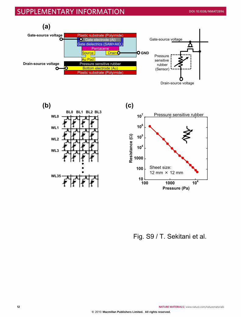
Figure S9. Pressure sensor system. a, Schematic cross-section of a pressure sensor sheet fabricated by laminating three sheets: (1) a foldable 4 36 array of pentacene TFTs,
(2) a pressure-sensitive rubber sheet (PCR Technical Co. Ltd, Japan), (3) a 12.5-μm-thick polyimide sheet with a gold
counter electrode. b, Circuit diagram of the array. The gate electrodes are connected to word lines (WL) and the drain contacts to bit lines (BL). c, Electrical resistance measured between the top and bottom surfaces of the pressure-
sensitive rubber sheet as a function of mechanical pressure. When pressure is applied to the rubber sheet, the resistance decreases from 1 M at 100 Pa to 100 at 10
4 Pa.
© 2010 Macmillan Publishers Limited. All rights reserved.
4 nature materials | www.nature.com/naturematerials
SUPPLEMENTARY INFORMATION doi: 10.1038/nmat2896
RMS = 2.2 nm
RMS = 1.3 nm
RMS = 11.9 nm
Al
AlOx
Pentaceneon SAM
0
5
10(nm)
(a) Si/SiO2 substrate(c) Polyimide substrate with planarization layer
1 μm2
1 μm2
Substratesurface
SAM
RMS = 0.71 nm
RMS = 0.63 nm
RMS = 10.9 nm
RMS = 0.7 nm
RMS = 0.38 nm1 μm2
0
5
10(nm)
0
50
100(nm)
0
5
10(nm)
0
5
10(nm)
50
100(nm)
10 μm2
RMS = 0.32 nm10 μm2
0
5
10(nm)
(b) Polyimide substrate without planarization layer
RMS = 2.5 nm10 μm2
0
15
30(nm)
RMS = 3.5 nm1 μm2
0
5
10(nm)
RMS = 3.8 nm10 μm2
0
25
50(nm)
RMS = 3.0 nm10 μm2
0
25
30(nm)
RMS = 1.2 nm10 μm210 μm2
0
5
10(nm)
10 μm2
10 μm2
RMS = 10.7 nm10 μm2
0
50
100(nm)
10 μm2 10 μm20
0
5
10(nm)
0
5
10(nm)
Fig. S1 / T. Sekitani et al.
© 2010 Macmillan Publishers Limited. All rights reserved.
nature materials | www.nature.com/naturematerials 5
SUPPLEMENTARY INFORMATIONdoi: 10.1038/nmat2896
Fig. S2 / T. Sekitani et al.
(a)
(b)
Source & drain contacts (Au)
Gate electrode (Al) Substrate (Si/SiO2)
SAM
Organicsemiconductor(Pentacene)
AlOx
SAM (2 nm)AlOx (4 nm)Al (18 nm)
Pentacene
Si/SiO220 nm
SAM
AlOx
Source & drain contacts (Au)
Gate electrode (Al) Polyimide substrate without planarization layer
Organicsemiconductor(Pentacene)
SAM (2 nm)AlOx (4 nm)
Al (18 nm)
Pentacene
Polyimide (Substrate)
20 nm
(c)
SAM (2 nm)AlOx (4 nm)Al (18 nm)
Pentacene
Polyimide (planarization layer)
20 nm
SAM
AlOx
Source & drain contacts (Au)
Gate electrode (Al)
Organicsemiconductor(Pentacene)
Polyimide substrate with planarization layer
© 2010 Macmillan Publishers Limited. All rights reserved.
6 nature materials | www.nature.com/naturematerials
SUPPLEMENTARY INFORMATION doi: 10.1038/nmat2896
Fig. S3 / T. Sekitani et al.
10-12
10-11
10-10
10-9
10-8
10-7
10-6
10-5
10-12
10-11
10-10
10-9
10-8
10-7
10-6
10-5
-2.5 -2 -1.5 -1 -0.5 0
Dra
in c
urre
nt (A
) Gate current (A
)
Gate-source votage (V)
VGS = 1 to - 2 V VDS = -2 V-0.2
-0.1
0-2 -1.5 -1 -0.5 0
Dra
in c
urre
nt (μ
A)
Drain-source voltage (V)
Source & drain contacts (Au)
Gate electrode (Al)Polyimide substrate
(without planarization layer)
SAM
Organicsemiconductor
© 2010 Macmillan Publishers Limited. All rights reserved.
nature materials | www.nature.com/naturematerials 7
SUPPLEMENTARY INFORMATIONdoi: 10.1038/nmat2896
Fig. S4 / T. Sekitani et al.
R=150 μm
Stage
Push Plate
TFTs on film
Stage
Push Plate
TFTs on film
(b)
(a)
(c)
Gold wire
© 2010 Macmillan Publishers Limited. All rights reserved.
8 nature materials | www.nature.com/naturematerials
SUPPLEMENTARY INFORMATION doi: 10.1038/nmat2896
0.8
0.85
0.9
0.95
1
1.05
0.30.40.50.60.70.80.91
C/C
0
Bending radius (mm)
Fig. S5 / T. Sekitani et al.
with encapsulation
without encapsulation
© 2010 Macmillan Publishers Limited. All rights reserved.
nature materials | www.nature.com/naturematerials 9
SUPPLEMENTARY INFORMATIONdoi: 10.1038/nmat2896
10-11
10-10
10-9
10-8
0.010.1110
Gat
e cu
rren
t (A
)
Bending radius (mm)
0
0.2
0.4
0.6
0.8
1
1.2
0.010.1110
Nor
mal
ized
dra
in c
urre
nt
Bending radius (mm)
(b) (c)
Fig. S6 / T. Sekitani et al.
75-μm-thick polyimide substrate
(a)
Au(D)Au(S)Pentacene
Au(G)
PolyimideSAM/AlOx
Current // Strain
Current ⊥Strain
Current // Strain
Current ⊥Strain
© 2010 Macmillan Publishers Limited. All rights reserved.
10 nature materials | www.nature.com/naturematerials
SUPPLEMENTARY INFORMATION doi: 10.1038/nmat2896
10-12
10-11
10-10
10-9
10-8
10-7
10-6
10-5
-3 -2.5 -2 -1.5 -1 -0.5 0
Dra
in c
urre
nt (A
)
Gate-source voltage (V)
Fig. S7 / T. Sekitani et al.
R= ∞ (Initial)R= 200 μm
VDS = -2 V
R= ∞ after 200 μm-bending
-2.0
-1.5
-1.0
-0.5
0-3 -2.5 -2 -1.5 -1 -0.5 0
Dra
in c
urre
nt (μ
A)
Drain-source voltage (V)
R= ∞ (Initial)R= 200 μmR= ∞ after 200 μm-bending
VGS = 0 V to – 3 V
© 2010 Macmillan Publishers Limited. All rights reserved.
nature materials | www.nature.com/naturematerials 11
SUPPLEMENTARY INFORMATIONdoi: 10.1038/nmat2896
Fig. S8 / T. Sekitani et al.
Complementary five stage ring oscillatorVDD
1
10
100
1000
1 1.5 2 2.5 3 3.5
Sign
al d
elay
per
sta
ge (m
s)
Supply voltage VDD (V)
L = 50 μm
L = 20 μm
© 2010 Macmillan Publishers Limited. All rights reserved.
12 nature materials | www.nature.com/naturematerials
SUPPLEMENTARY INFORMATION doi: 10.1038/nmat2896
Fig. S9 / T. Sekitani et al.
(a)
(c)
Bottom electrode (Au)Plastic substrate (Polyimide)
Pressure sensitive rubberDrain-source voltage
10
100
1000
104
105
106
107
100 1000 104
Res
ista
nce
(Ω)
Pressure (Pa)
Sheet size: 12 mm × 12 mm
Pressure sensitive rubber
Gate electrode (Al)Plastic substrate (Polyimide)
PentaceneGate dielectrics (SAM+AlOx)
Source Drain
Au Pad
GND
Gate-source voltage
Pressuresensitive
rubber(Sensor)
Drain-source voltage
Gate-source voltage
(b)WL0
WL1
WL2
WL3
WL35
BL0 BL1 BL2 BL3
© 2010 Macmillan Publishers Limited. All rights reserved.